a 74.33 db sndr 20 msps 2.74 mw pipelined adc using a
TRANSCRIPT
A 74.33 dB SNDR 20 MSPS 2.74 mWPipelined ADC using a Dynamic
Deadzone Ring Amplifier
May 1, 2017
by Spencer Leuenberger, Jason Muhlestein, Hyuk Sun, Praveen Kumar Venkatachala, and Un-Ku Moon
Oregon State University
Table of Contents
May 1, 2017
1
• Introduction & Motivation
• Prior Work – Ring Amplifiers
• Current-Starved Inverter
• Ring Amplifier w/ Dynamic Deadzone
• Pipeline Architecture
• Measurements
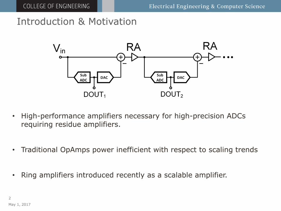
Introduction & Motivation
May 1, 2017
2
• High-performance amplifiers necessary for high-precision ADCs requiring residue amplifiers.
• Traditional OpAmps power inefficient with respect to scaling trends
• Ring amplifiers introduced recently as a scalable amplifier.
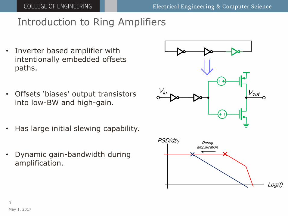
Introduction to Ring Amplifiers
May 1, 2017
3
• Inverter based amplifier with intentionally embedded offsets paths.
• Offsets ‘biases’ output transistors into low-BW and high-gain.
• Has large initial slewing capability.
• Dynamic gain-bandwidth during amplification.
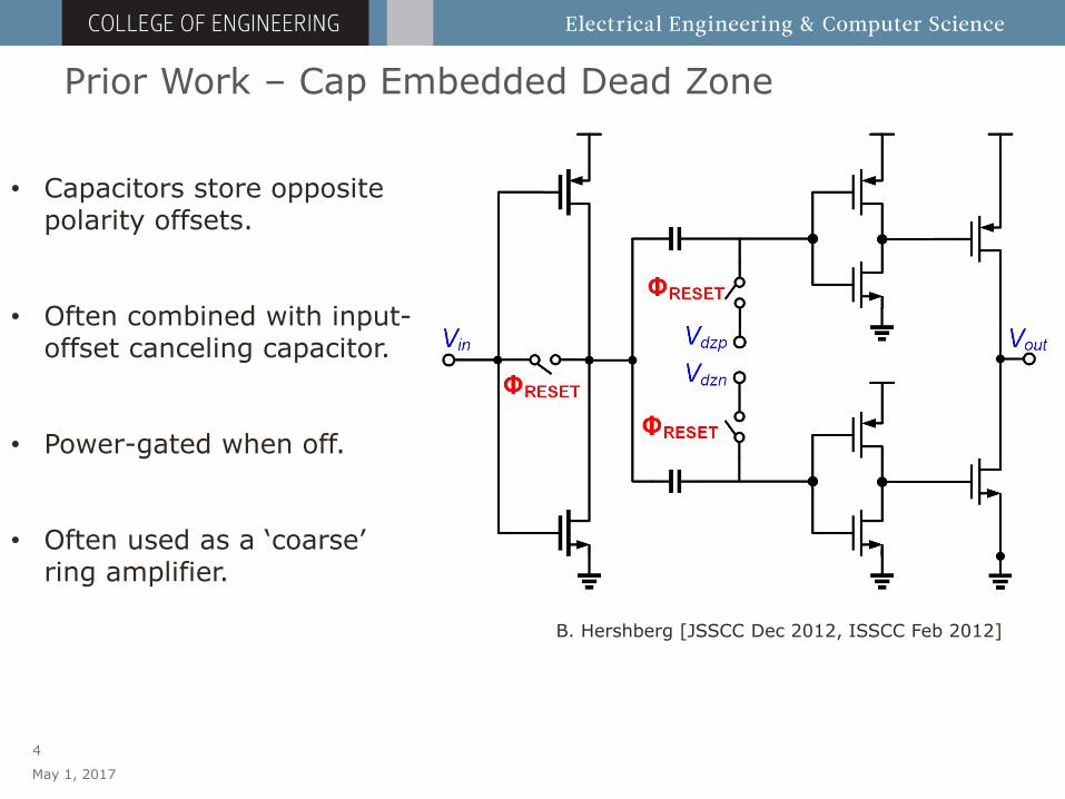
Prior Work – Cap Embedded Dead Zone
May 1, 2017
4
• Capacitors store opposite polarity offsets.
• Often combined with input-offset canceling capacitor.
• Power-gated when off.
• Often used as a ‘coarse’ ring amplifier.
B. Hershberg [JSSCC Dec 2012, ISSCC Feb 2012]
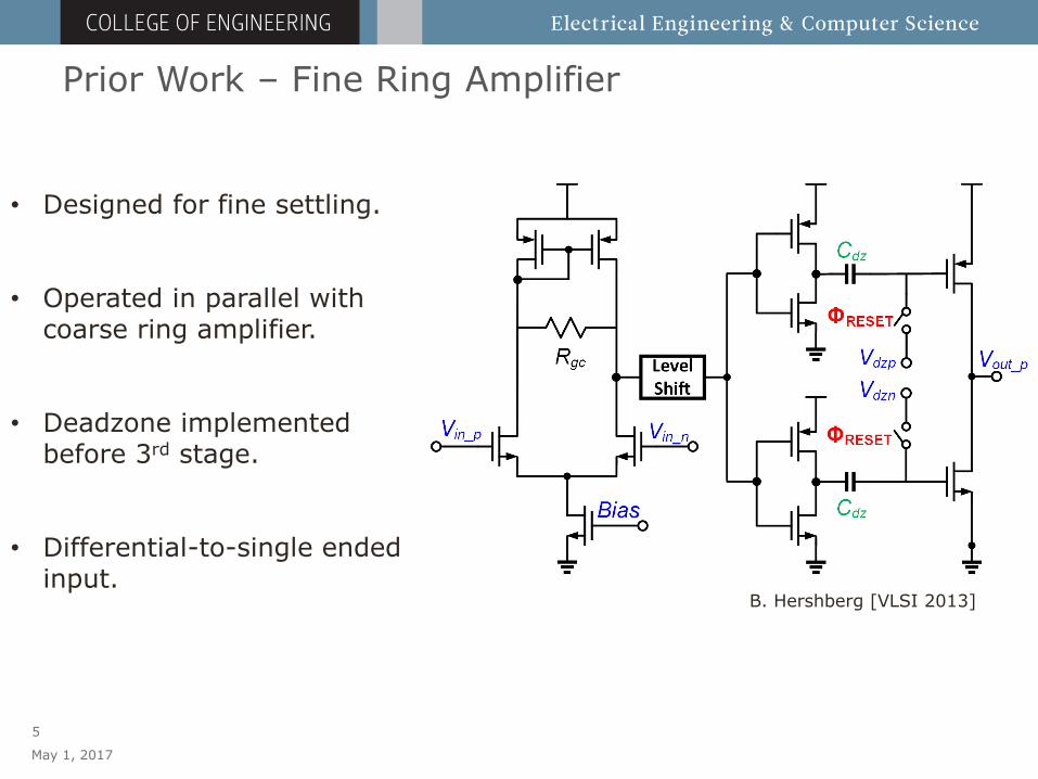
Prior Work – Fine Ring Amplifier
May 1, 2017
5
• Designed for fine settling.
• Operated in parallel with coarse ring amplifier.
• Deadzone implemented before 3rd stage.
• Differential-to-single ended input.
B. Hershberg [VLSI 2013]
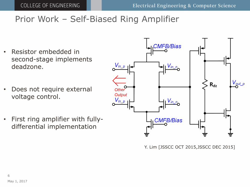
Prior Work – Self-Biased Ring Amplifier
May 1, 2017
6
Y. Lim [JSSCC OCT 2015,JSSCC DEC 2015]
• Resistor embedded in second-stage implements deadzone.
• Does not require external voltage control.
• First ring amplifier with fully-differential implementation
Motivation
May 1, 2017
7
• Unknown noise performance of ring amplifiers.
• Coarse and fine ring amplifiers take up extra area.
Want
• A ring-amplifier noise limited ADC
• A continually tunable dead zone.
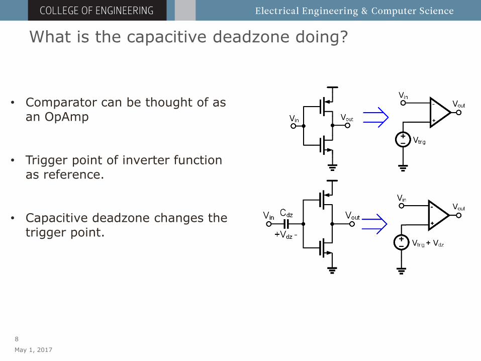
What is the capacitive deadzone doing?
May 1, 2017
8
• Comparator can be thought of as an OpAmp
• Trigger point of inverter function as reference.
• Capacitive deadzone changes the trigger point.
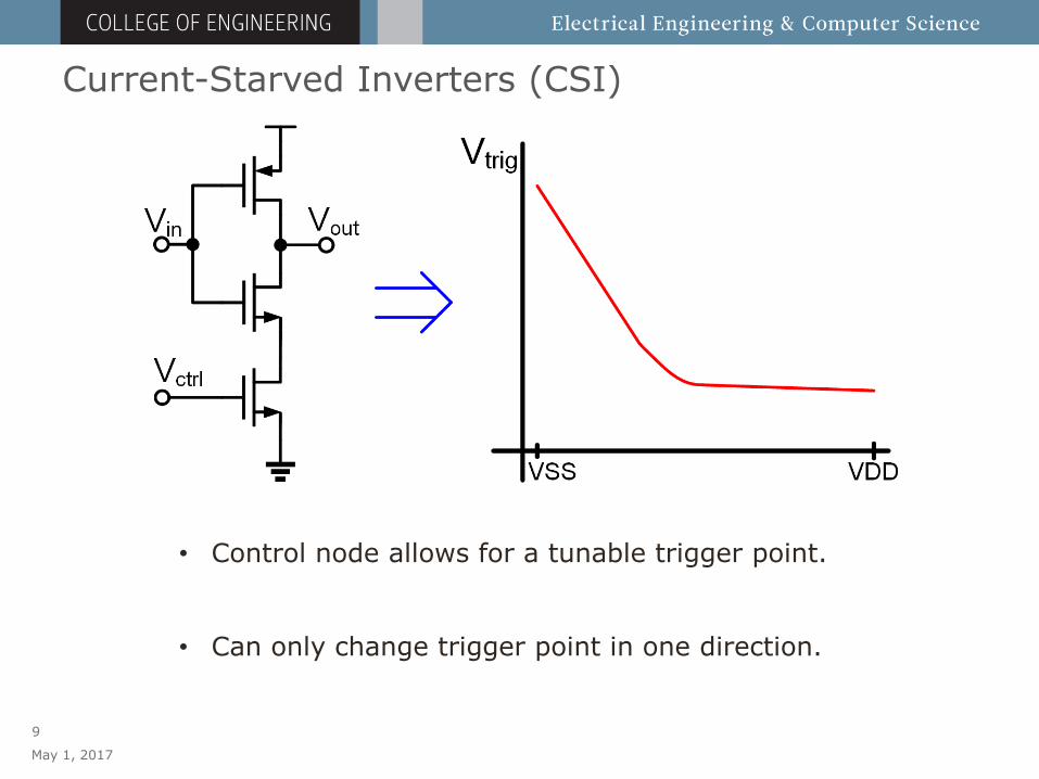
Current-Starved Inverters (CSI)
May 1, 2017
9
• Control node allows for a tunable trigger point.
• Can only change trigger point in one direction.
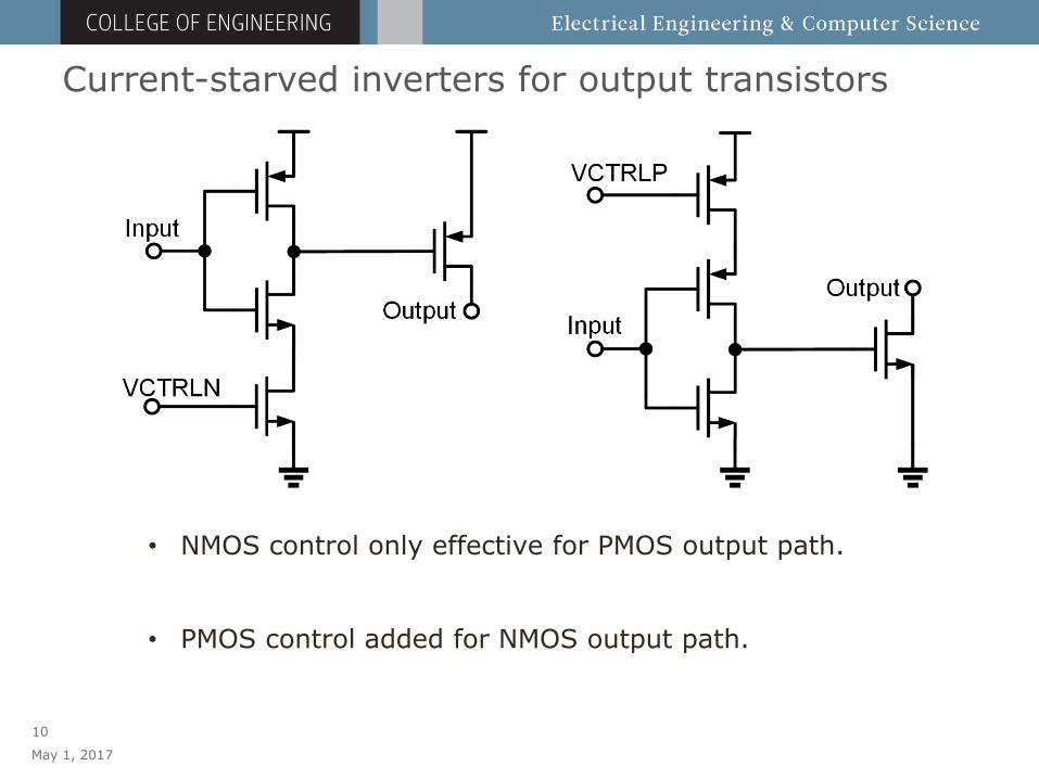
Current-starved inverters for output transistors
May 1, 2017
10
• NMOS control only effective for PMOS output path.
• PMOS control added for NMOS output path.
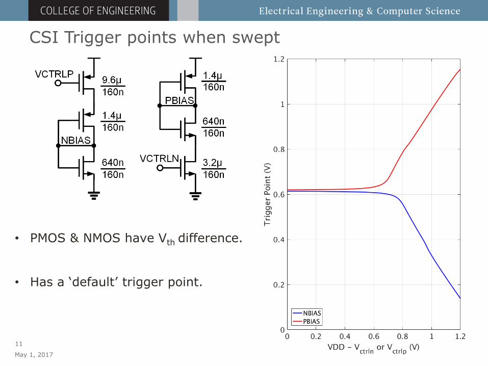
CSI Trigger points when swept
May 1, 2017
11
• PMOS & NMOS have Vth difference.
• Has a ‘default’ trigger point.
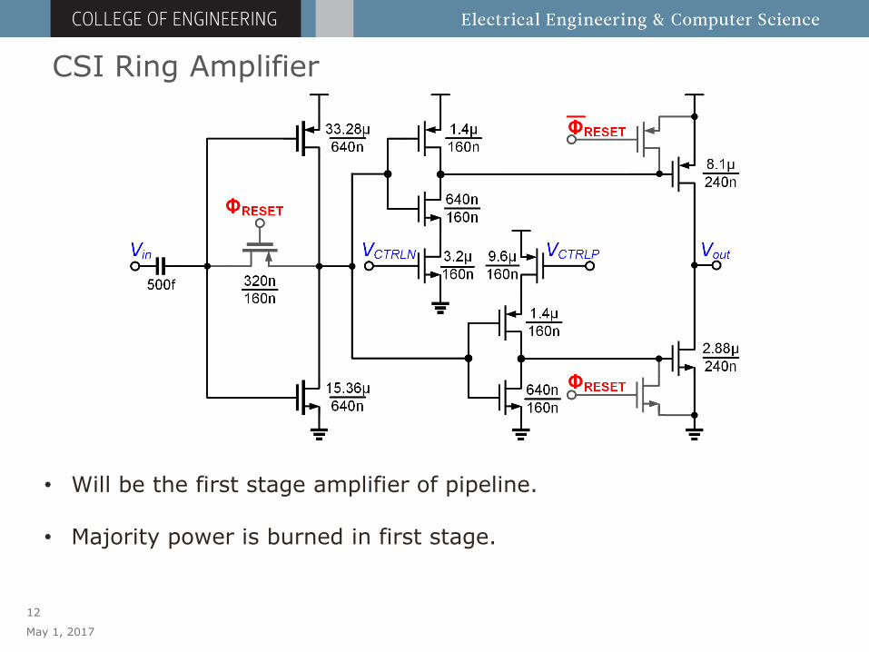
CSI Ring Amplifier
May 1, 2017
12
• Will be the first stage amplifier of pipeline.
• Majority power is burned in first stage.
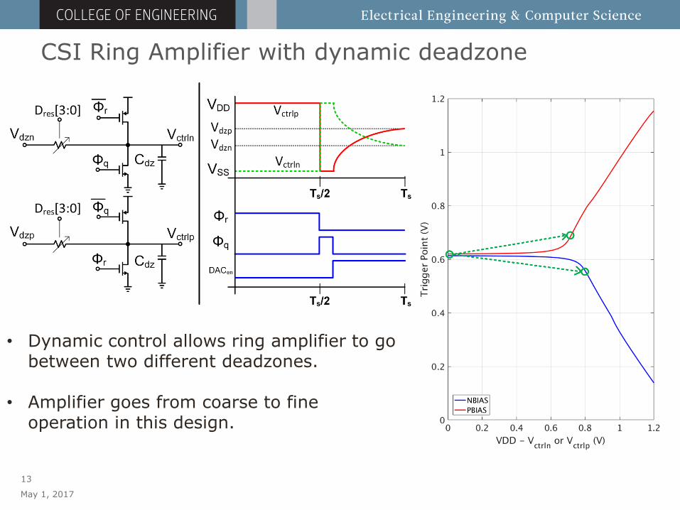
CSI Ring Amplifier with dynamic deadzone
May 1, 2017
13
• Dynamic control allows ring amplifier to go between two different deadzones.
• Amplifier goes from coarse to fine operation in this design.
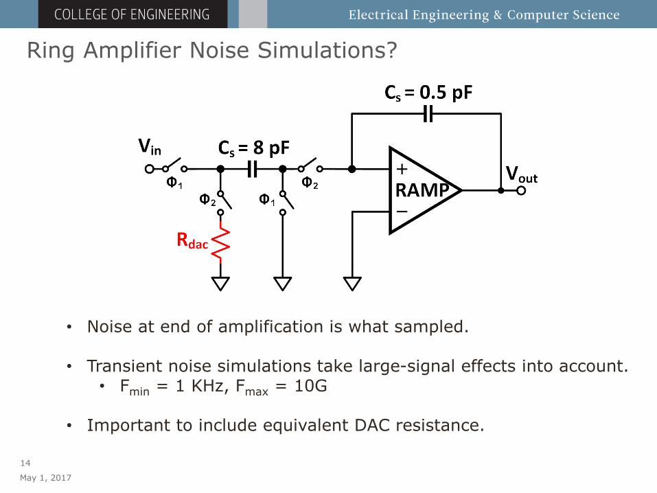
Ring Amplifier Noise Simulations?
May 1, 2017
14
• Noise at end of amplification is what sampled.
• Transient noise simulations take large-signal effects into account.• Fmin = 1 KHz, Fmax = 10G
• Important to include equivalent DAC resistance.
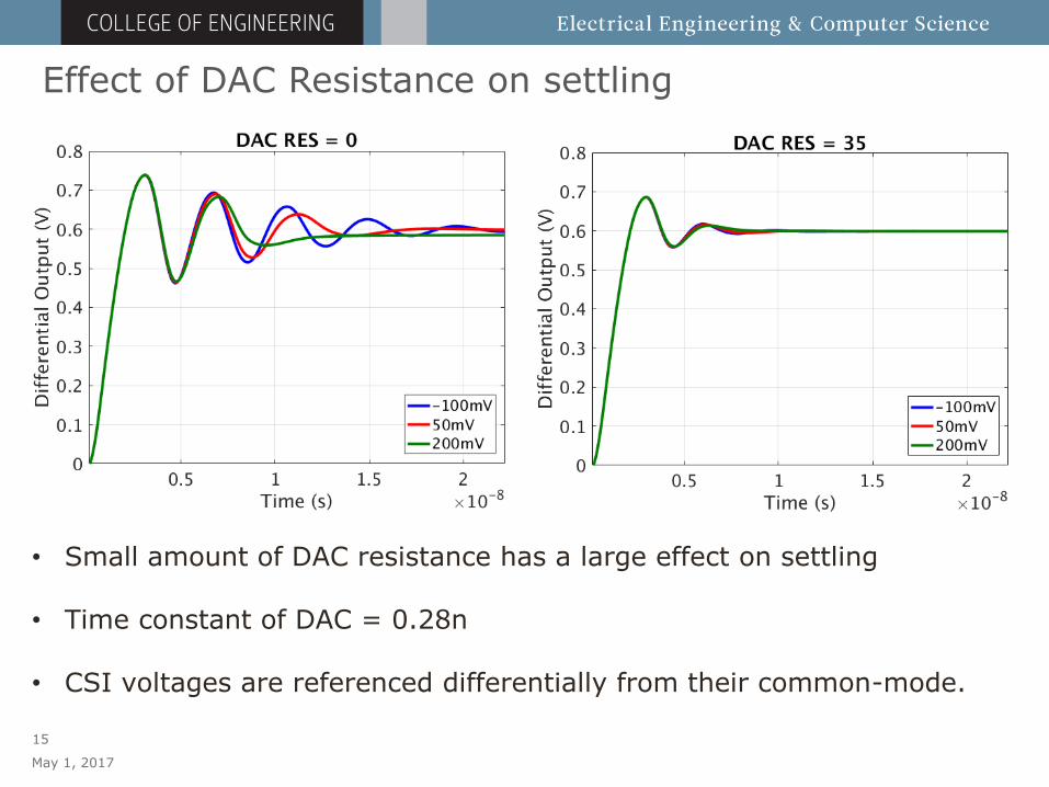
Effect of DAC Resistance on settling
May 1, 2017
15
• Small amount of DAC resistance has a large effect on settling
• Time constant of DAC = 0.28n
• CSI voltages are referenced differentially from their common-mode.
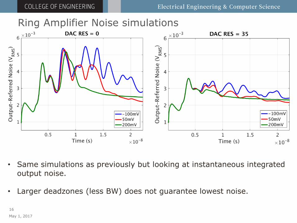
Ring Amplifier Noise simulations
May 1, 2017
16
• Same simulations as previously but looking at instantaneous integrated output noise.
• Larger deadzones (less BW) does not guarantee lowest noise.
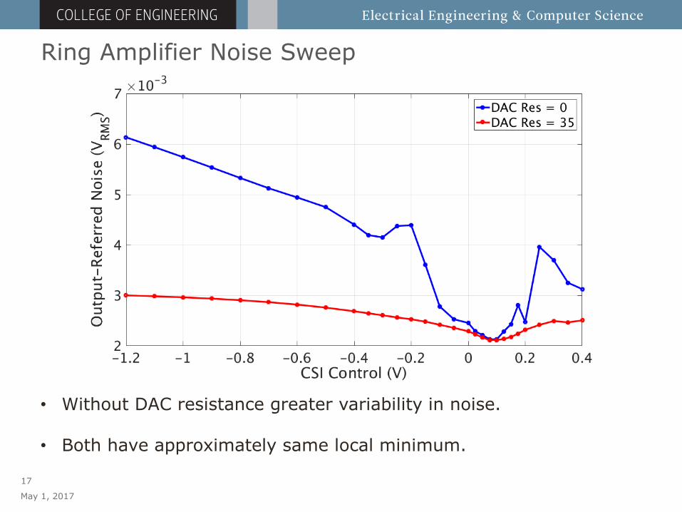
Ring Amplifier Noise Sweep
May 1, 2017
17
• Without DAC resistance greater variability in noise.
• Both have approximately same local minimum.
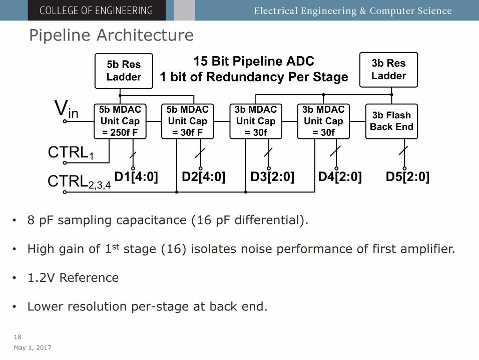
Pipeline Architecture
May 1, 2017
18
• 8 pF sampling capacitance (16 pF differential).
• High gain of 1st stage (16) isolates noise performance of first amplifier.
• 1.2V Reference
• Lower resolution per-stage at back end.
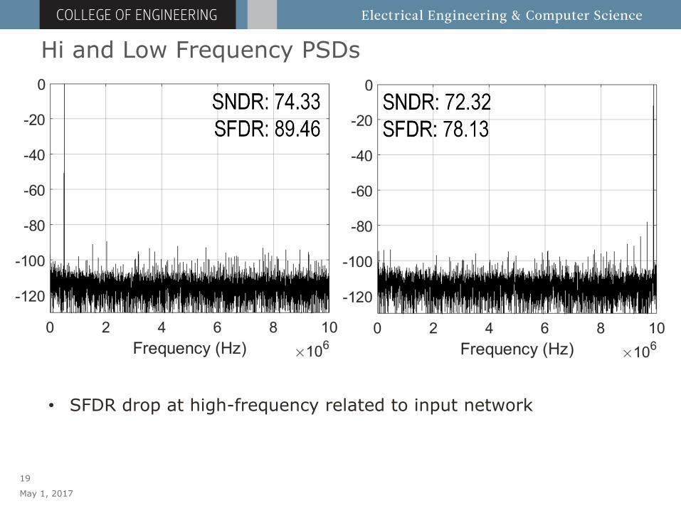
Hi and Low Frequency PSDs
May 1, 2017
19
• SFDR drop at high-frequency related to input network
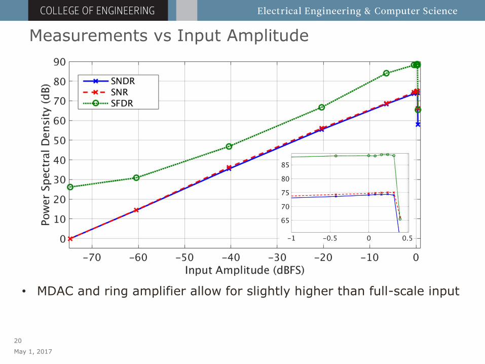
Measurements vs Input Amplitude
May 1, 2017
20
• MDAC and ring amplifier allow for slightly higher than full-scale input
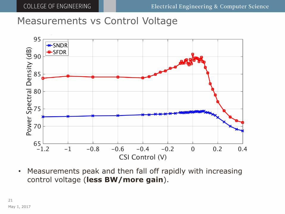
Measurements vs Control Voltage
May 1, 2017
21
• Measurements peak and then fall off rapidly with increasing control voltage (less BW/more gain).
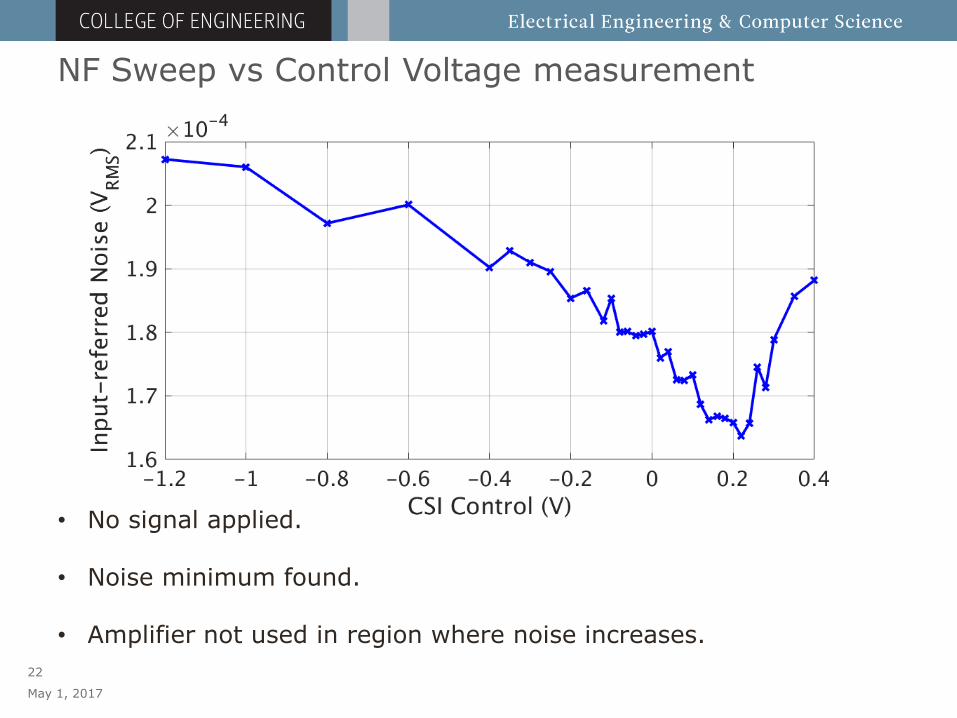
NF Sweep vs Control Voltage measurement
May 1, 2017
22
• No signal applied.
• Noise minimum found.
• Amplifier not used in region where noise increases.
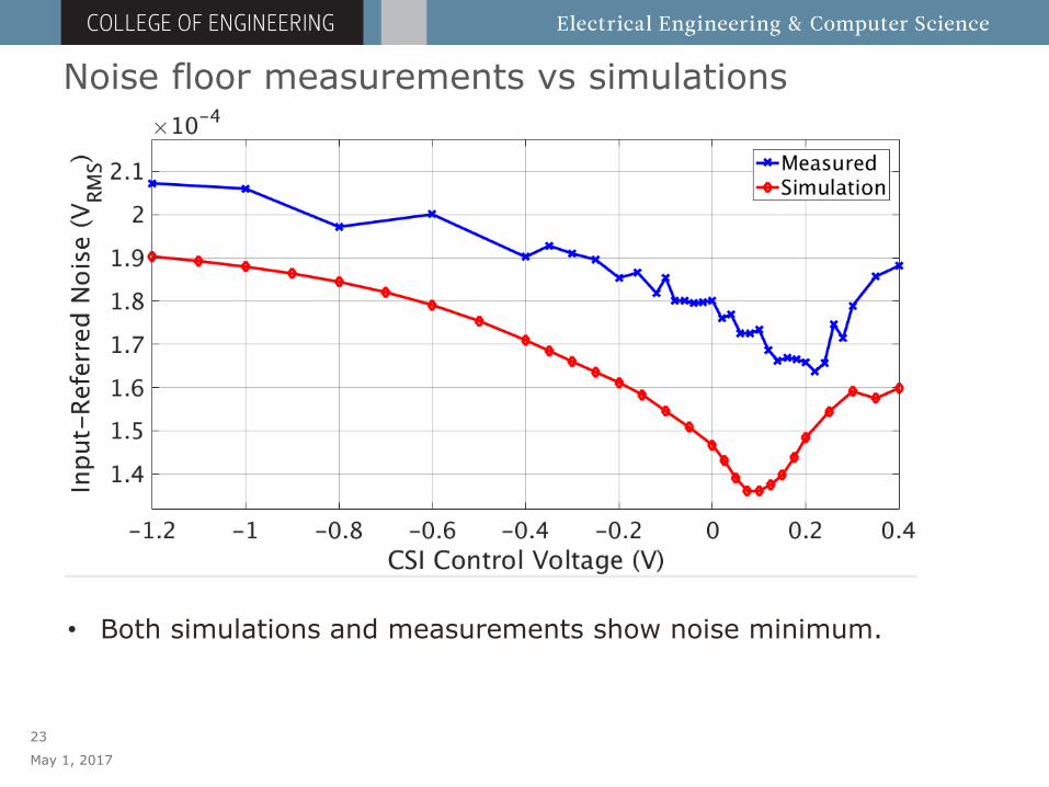
Noise floor measurements vs simulations
May 1, 2017
23
• Both simulations and measurements show noise minimum.
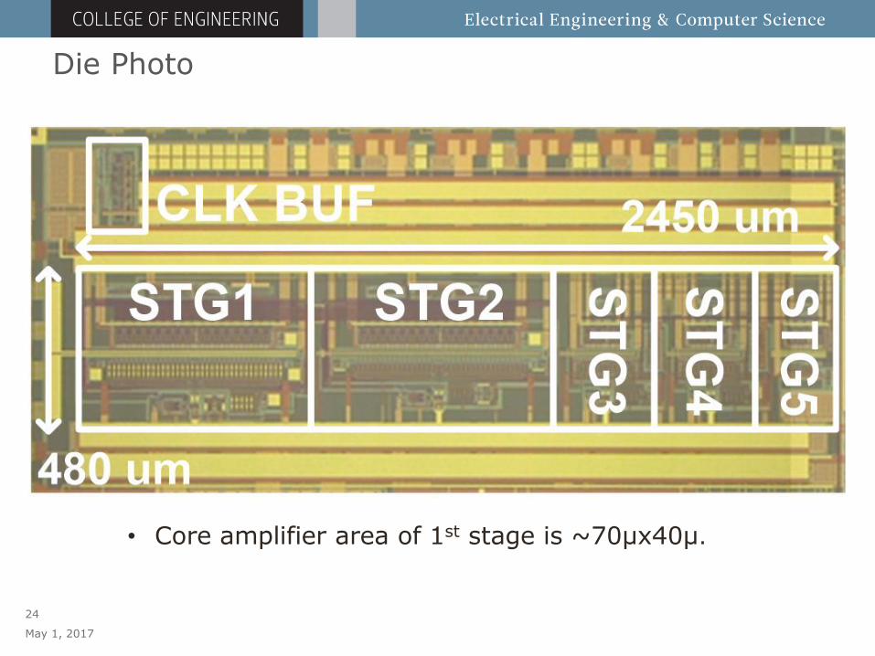
Die Photo
May 1, 2017
24
• Core amplifier area of 1st stage is ~70µx40µ.
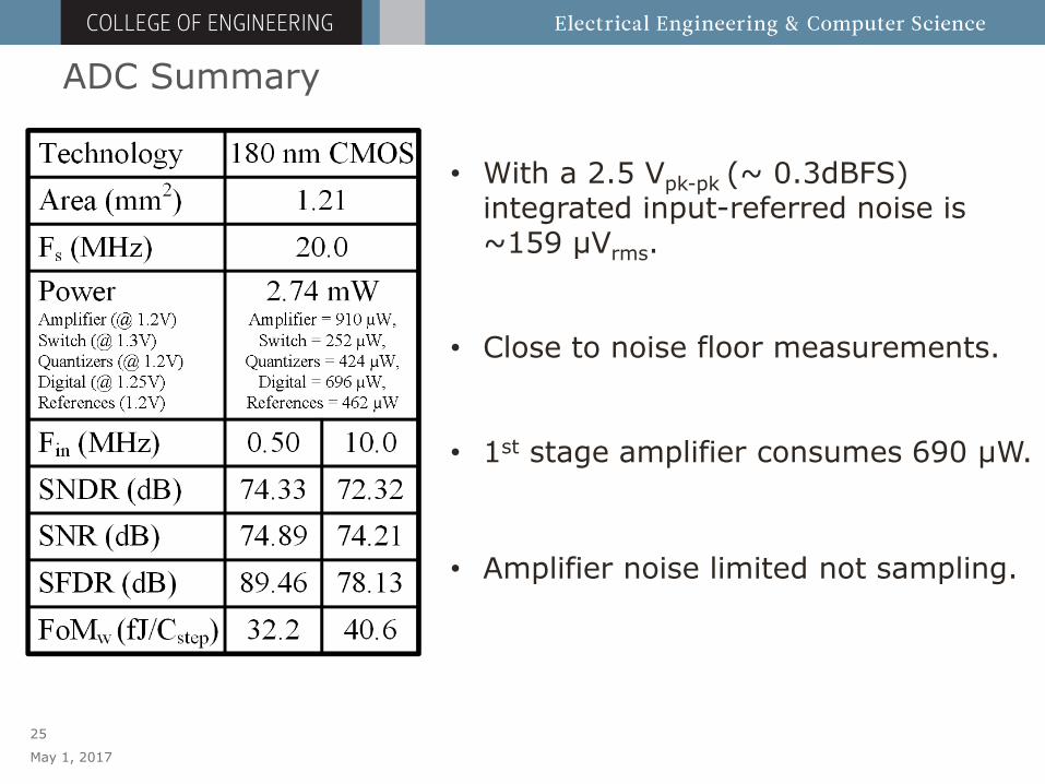
ADC Summary
May 1, 2017
25
• With a 2.5 Vpk-pk (~ 0.3dBFS) integrated input-referred noise is ~159 µVrms.
• Close to noise floor measurements.
• 1st stage amplifier consumes 690 µW.
• Amplifier noise limited not sampling.
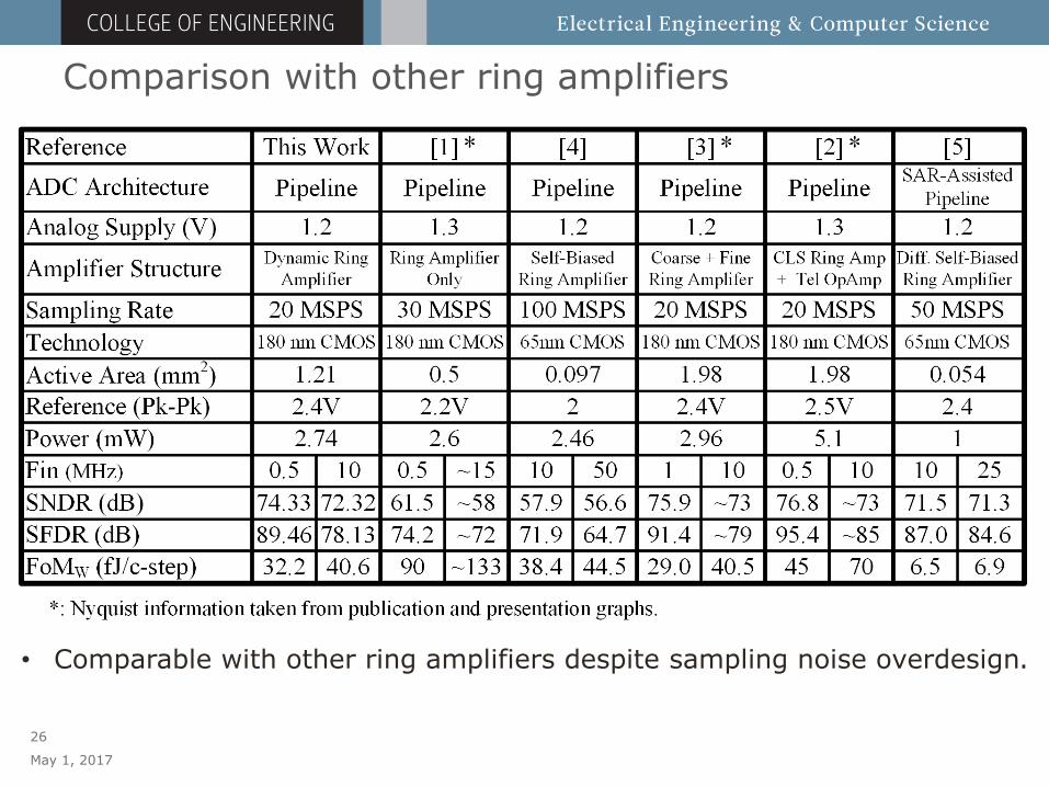
Comparison with other ring amplifiers
May 1, 2017
26
• Comparable with other ring amplifiers despite sampling noise overdesign.

Conclusions
May 1, 2017
27
Acknowledgements
• Thanks to Asahi Kasei Microdevices for fabrication and packaging
• Current-starved inverter ring amplifier introduced.
• Dynamic deadzone that automatically increases deadzoneduring amplification was presented.
• Transient noise simulations verified to capture large-signal behavior of ring amplifiers.
Backup
May 1, 2017
28
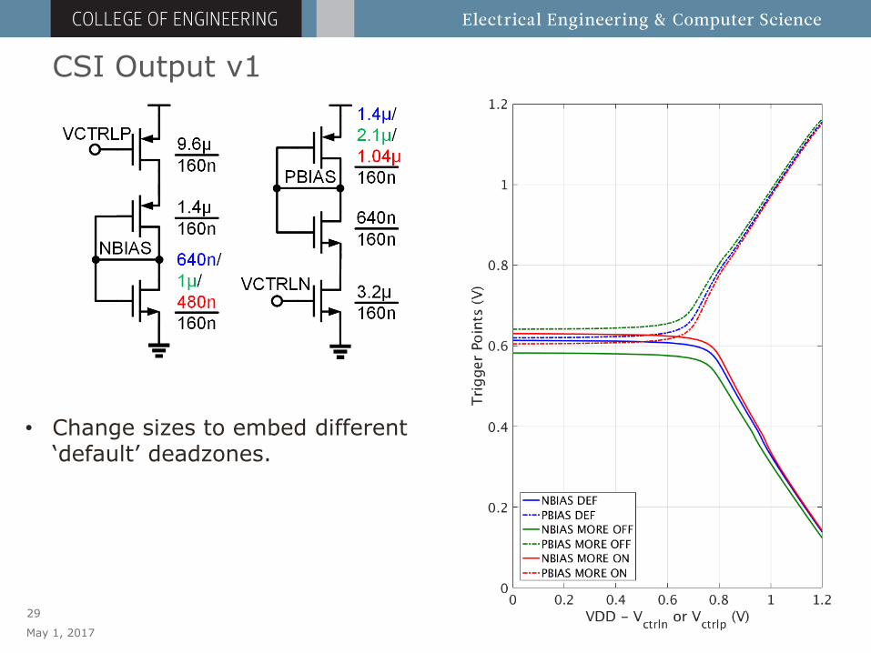
CSI Output v1
May 1, 2017
29
• Change sizes to embed different ‘default’ deadzones.
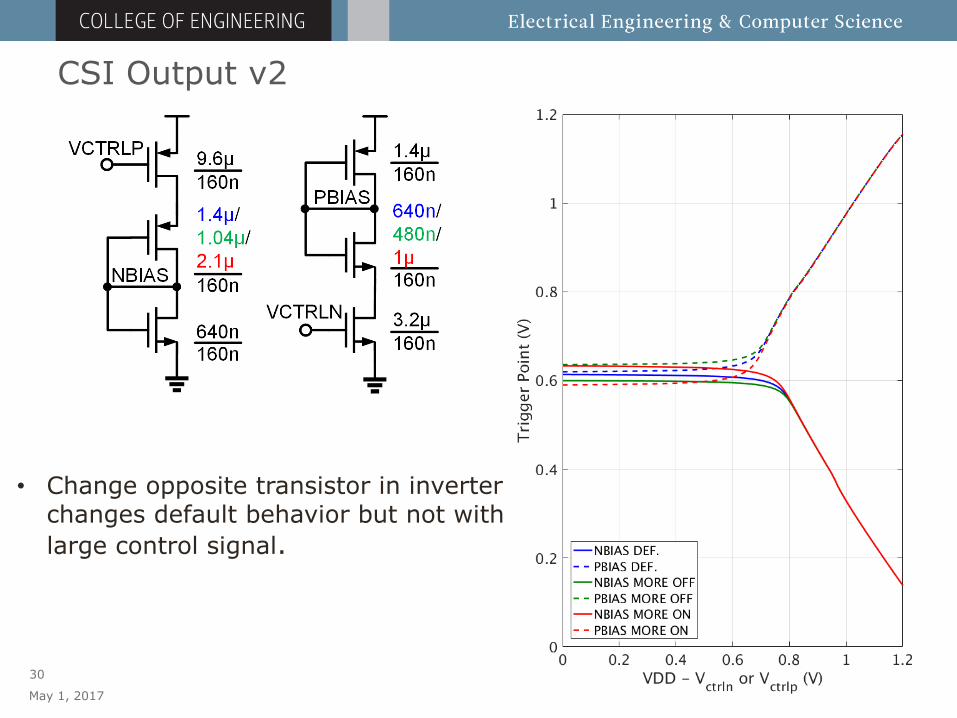
CSI Output v2
May 1, 2017
30
• Change opposite transistor in inverter changes default behavior but not with
large control signal.
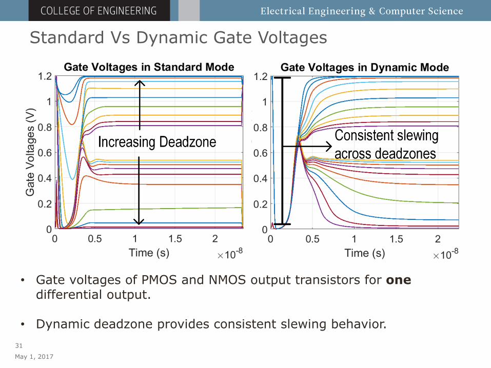
Standard Vs Dynamic Gate Voltages
May 1, 2017
31
• Gate voltages of PMOS and NMOS output transistors for onedifferential output.
• Dynamic deadzone provides consistent slewing behavior.
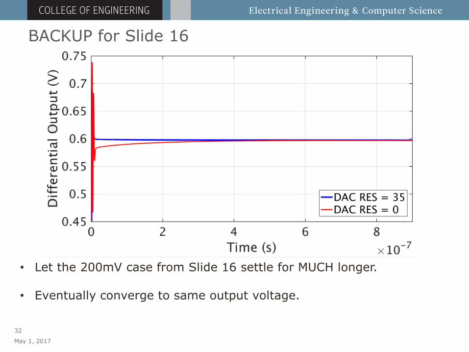
BACKUP for Slide 16
May 1, 2017
32
• Let the 200mV case from Slide 16 settle for MUCH longer.
• Eventually converge to same output voltage.
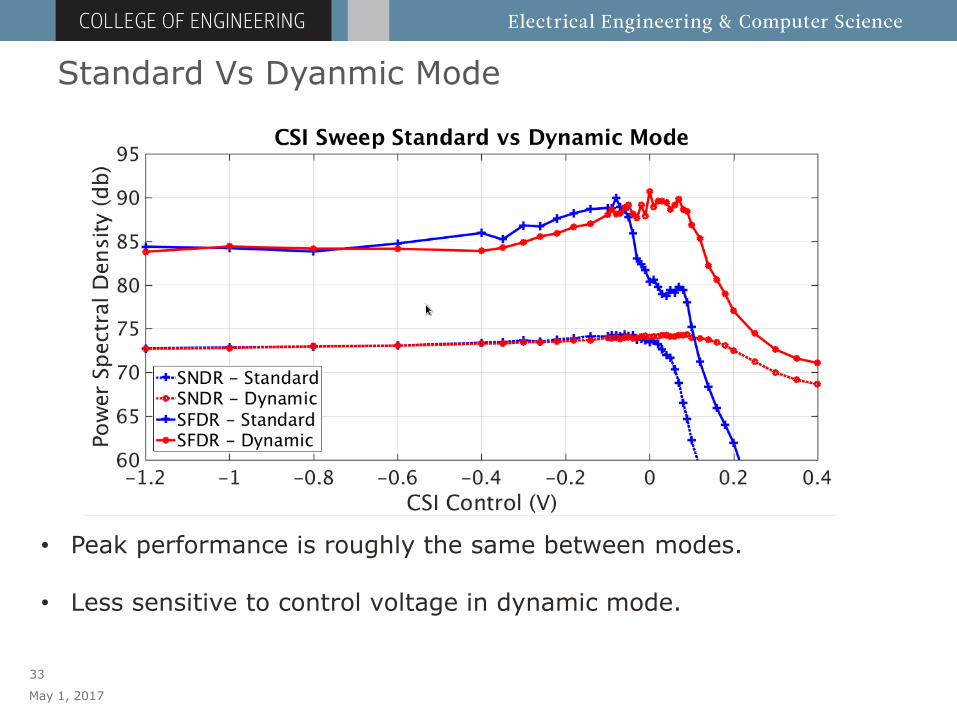
Standard Vs Dyanmic Mode
May 1, 2017
33
• Peak performance is roughly the same between modes.
• Less sensitive to control voltage in dynamic mode.
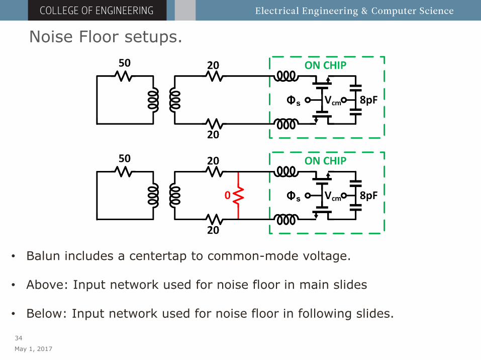
Noise Floor setups.
May 1, 2017
34
• Balun includes a centertap to common-mode voltage.
• Above: Input network used for noise floor in main slides
• Below: Input network used for noise floor in following slides.
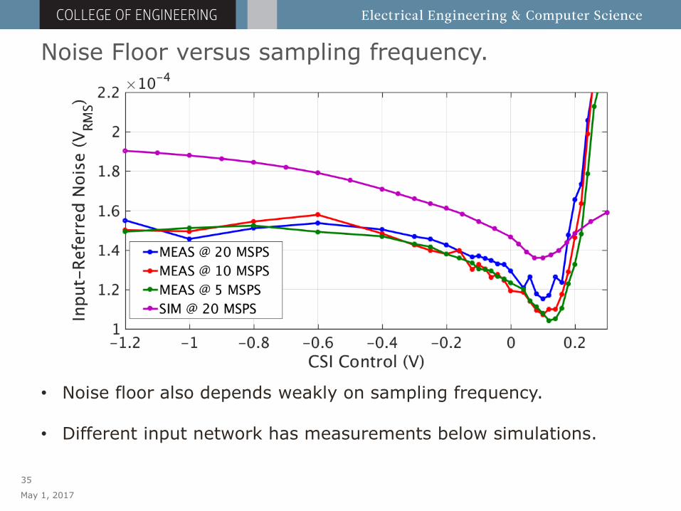
Noise Floor versus sampling frequency.
May 1, 2017
35
• Noise floor also depends weakly on sampling frequency.
• Different input network has measurements below simulations.