16-bit, 2 msps/1 msps/500 ksps, precision, pseudo ... · 16-bit, 2 msps/1 msps/500 ksps, precision,...
TRANSCRIPT

16-Bit, 2 MSPS/1 MSPS/500 kSPS, Precision, Pseudo Differential, SAR ADCs
Data Sheet AD4000/AD4004/AD4008
Rev. D Document Feedback Information furnished by Analog Devices is believed to be accurate and reliable. However, no responsibility is assumed by Analog Devices for its use, nor for any infringements of patents or other rights of third parties that may result from its use. Specifications subject to change without notice. No license is granted by implication or otherwise under any patent or patent rights of Analog Devices. Trademarks and registered trademarks are the property of their respective owners.
One Technology Way, P.O. Box 9106, Norwood, MA 02062-9106, U.S.A.Tel: 781.329.4700 ©2016–2019 Analog Devices, Inc. All rights reserved. Technical Support www.analog.com
FEATURES Throughput: 2 MSPS/1 MSPS/500 kSPS options INL: ±1.0 LSB maximum Guaranteed 16-bit, no missing codes Low power
4.9 mW/MSPS, 2.5 mW at 500 kSPS, VDD only 7 mW/MSPS, 70 μW at 10 kSPS, 14 mW at 2 MSPS, total
SNR: 93 dB typical at fIN = 1 kHz, 90 dB typical at fIN = 100 kHz Oversampled SNR
96 dB at 1.0 MSPS, OSR = 2 123 dB at 1.9 kSPS, OSR = 1024
THD: −115 dB typical at fIN = 1 kHz, VREF = 5 V; −95 dB typical at fIN = 100 kHz
SINAD: 82 dB at fIN = 1 MHz Easy Drive Greatly reduced input kickback
Input current reduced to 0.4 μA/MSPS Long acquisition phase, ≥79% of cycle time at 1 MSPS Input span compression for single-supply operation Fast conversion time allows low SPI clock rates Input overvoltage clamp protection sinks up to 50 mA
Pseudo differential input range 0 V to VREF with VREF from 2.4 V to 5.1 V
Single 1.8 V supply operation with 1.71 V to 5.5 V logic interface First conversion accurate SPI-/QSPI-/MICROWIRE-/DSP-compatible serial interface Ability to daisy-chain multiple ADCs Guaranteed operation: −40°C to +125°C 10-lead packages: 3 mm × 3 mm LFCSP, 3 mm × 4.90 mm MSOP Pin compatible with AD4003/AD4007/AD4011 family
APPLICATIONS Automatic test equipment Machine automation Medical equipment Battery-powered equipment Precision data acquisition systems
FUNCTIONAL BLOCK DIAGRAM
GND
IN+
IN–
SDI
SCK
SDO
CNV
AD4000/AD4004/AD4008
16-BITSAR ADC
SERIALINTERFACE
VIO
REF VDD
VREF
0VREF/2
HIGH-ZMODE
CLAMP SPANCOMPRESSION
TURBOMODE
STATUSBITS
2.4V TO 5.1V 1.8V
10µF
1.8V TO 5V
3-WIRE OR 4-WIRESPI INTERFACE(DAISY CHAIN, CS)
14
956
-00
1
Figure 1.
GENERAL DESCRIPTION The AD4000/AD4004/AD4008 are high accuracy, high speed, low power, 16-bit, Easy Drive, precision successive approximation register (SAR) analog-to-digital converters (ADCs). The high throughput allows both accurate capture of high frequency signals and decimation to achieve higher SNR, while reducing antialiasing filter challenges. Easy Drive features reduce signal chain complexity and power consumption, and enable higher channel density. The reduced input current, particularly in high-Z mode, coupled with a long signal acquisition phase, eliminates the need for a dedicated high power, high speed ADC driver, which broadens the range of low power precision amplifiers that can drive these ADCs directly (see Figure 2). The input span compression feature enables the ADC driver amplifier and the ADC to operate off of common supply rails without the need for a negative supply while preserving the full ADC code range. The input overvoltage clamp protects the ADC inputs against overvoltage events, minimizes disturbance on the reference pin, and eliminates the need for external protection diodes. The low serial peripheral interface (SPI) clock rate (70 MHz for the AD4000 at 2 MSPS in turbo mode) reduces the digital input/output power consumption, broadens processor options, and simplifies the task of sending data across digital isolation.
The SPI-compatible versatile serial interface features seven programmable modes with an optional busy indicator. Using the SDI input, several ADCs can be daisy-chained on a single 3-wire bus. The AD4000/AD4004/AD4008 are compatible with 1.8 V, 2.5 V, 3 V, and 5 V logic, using the separate supply, VIO.
–25
–20
–15
–10
–5
0
5
10
15
20
25
0 0.5 1.0 1.5 2.0 2.5 3.0 3.5 4.0 4.5 5.0
INP
UT
CU
RR
EN
T (μ
A)
INPUT DIFFERENTIAL VOLTAGE (V)
HIGH-Z DISABLED, 2MSPSHIGH-Z ENABLED, 2MSPS
149
56-
102
Figure 2. Input Current vs. Input Differential Voltage

AD4000/AD4004/AD4008 Data Sheet
Rev. D | Page 2 of 38
TABLE OF CONTENTS Features .............................................................................................. 1 Applications ....................................................................................... 1
Functional Block Diagram .......................................................... 1 General Description ......................................................................... 1 Revision History ............................................................................... 2 Specifications ..................................................................................... 4
Timing Specifications .................................................................. 7 Timing Diagram ........................................................................... 8
Absolute Maximum Ratings ............................................................ 9 Thermal Resistance ...................................................................... 9 ESD Caution .................................................................................. 9
Pin Configurations and Function Descriptions ......................... 10 Typical Performance Characteristics ........................................... 11 Terminology .................................................................................... 17 Theory of Operation ...................................................................... 18
Circuit Information .................................................................... 18 Converter Operation .................................................................. 19 Transfer Functions...................................................................... 19
Applications Information .............................................................. 20 Typical Application Diagrams .................................................. 20
Analog Inputs ............................................................................. 21 Driver Amplifier Choice ........................................................... 22 Ease of Drive Features ............................................................... 22 Voltage Reference Input ............................................................ 24 Power Supply ............................................................................... 24 Digital Interface .......................................................................... 24 Register Read/Write Functionality........................................... 26 Status Bits .................................................................................... 28 CS Mode, 3-Wire Turbo Mode ................................................. 29 CS Mode, 3-Wire Without Busy Indicator ............................. 30 CS Mode, 3-Wire with Busy Indicator .................................... 31 CS Mode, 4-Wire Turbo Mode ................................................. 32 CS Mode, 4-Wire Without Busy Indicator ............................. 33 CS Mode, 4-Wire with Busy Indicator .................................... 34 Daisy-Chain Mode ..................................................................... 35 Layout Guidelines....................................................................... 36 Evaluating the AD4000/AD4004/AD4008 Performance .......... 36
Outline Dimensions ....................................................................... 37 Ordering Guide .......................................................................... 38
REVISION HISTORY 8/2019—Rev. C to Rev. D Added Figure 2; Renumbered Sequentially .................................. 1 Changes to Features Section and General Description Section .... 1 Added Figure 18 and Figure 21..................................................... 13 Added Figure 27, Figure 28, and Figure 29 ................................. 14 Added Figure 33 and Figure 35..................................................... 15 Changes to Figure 31 and Figure 32 ............................................. 15 Changes to Figure 38 ...................................................................... 18 Changes to Input Overvoltage Clamp Circuit Section .............. 21 Changes to High-Z Mode Section, Figure 45, and Figure 46 ... 23 Added Configuration Register Details Section and Serial Clock Frequency Requirements Section ................................................. 24 Changes to Digital Interface Section ............................................ 24 Deleted Table 12 and Table 13; Renumbered Sequentially ....... 25 Added Table 12 and Table 13; Renumbered Sequentially ......... 25 Changes to Register Read/Write Functionality Section and Figure 47 .......................................................................................... 26 Changes to Figure 48 ...................................................................... 27 Added Table 58 ............................................................................... 28 Changes to Status Bits Section ...................................................... 28 Changes to CS Mode, 3-Wire Turbo Mode Section and Figure 51 .......................................................................................... 29
Changes to CS Mode, 3-Wire Without Busy Indicator Section and Figure 53 ................................................................................... 30 Changes to CS Mode, 3-Wire with Busy Indicator Section and Figure 55 .......................................................................................... 31 Changes to CS Mode, 4-Wire Turbo Mode Section and Figure 57 .......................................................................................... 32 Changes to CS Mode, 4-Wire Without Busy Indicator Section and Figure 59 ................................................................................... 33 Changes to CS Mode, 4-Wire with Busy Indicator Section and Figure 61 .......................................................................................... 34 Changes to Daisy-Chain Mode Section and Figure 64 ............. 35 Updated Outline Dimensions ....................................................... 37 Changes to Ordering Guide .......................................................... 38 10/2017—Rev. B to Rev. C Changes to Features Section ............................................................ 1 Added Multiplexed Applications Section .................................... 21 Changes to Ordering Guide .......................................................... 36 Added Timing Diagram Section ..................................................... 8 Moved Figure 3 .................................................................................. 8
Data Sheet AD4000/AD4004/AD4008
Rev. D | Page 3 of 38
9/2017—Rev. A to Rev. B Added AD4008 ................................................................... Universal Changes to Title, Features Section, General Description Section, and Figure 1 ........................................................................................ 1 Changes to Table 1 ............................................................................ 4 Changes to Timing Specifications Section and Table 2................ 7 Changes to Table 4 ............................................................................ 8 Changes to Table 5 ............................................................................ 9 Changes to Typical Performance Characteristics Section Layout .. 11 Changes to Figure 19 ............................................................................... 13 Added Figure 25; Renumbered Sequentially ............................... 14 Changes to Figure 28 ...................................................................... 14 Change to Zero Error Definition, Terminology Section............ 16 Changes to Circuit Information Section and Table 8 ................. 17 Changes to Converter Operation Section and Note 1 and Note 2, Table 9 ................................................................................. 18 Changes to High Frequency Input Signals Section, Figure 36 Caption, and Figure 37 Caption .................................................... 21 Added Figure 38 .............................................................................. 21 Changes to Input Span Compression Section, High-Z Mode Section, Figure 40, and Figure 41 Caption ................................... 22 Changes to Figure 42 Caption, Figure 43 Caption, Power Supply Section, and Figure 44 Caption ..................................................... 23 Changes to Figure 45, Digital Interface Section, and Table 11 ........ 24 Changes to Register Read/Write Functionality Section and Figure 46 Caption ............................................................................ 25 Changes to CS Mode, 3-Wire Turbo Mode Section ................... 28 Changes to CS Mode, 3-Wire with Busy Indicator Section ....... 30 Changes to CS Mode, 4-Wire Turbo Mode Section ................... 31 Changes to CS Mode, 4-Wire with Busy Indicator Section ....... 33 Changes to Daisy-Chain Mode Section ....................................... 34 Changed Evaluating the AD4000/AD4004 Performance Section to Evaluating the AD4000/AD4004/AD4008 Performance Section .............................................................................................. 35 Changes to Evaluating the AD4000/AD4004/AD4008 Performance Section ....................................................................... 35 Changes to Ordering Guide ........................................................... 36
4/2017—Rev. 0 to Rev. A Added AD4004 ................................................................... Universal Changes to Title, Features Section, General Description Section, and Figure 1 ....................................................................................... 1 Changes to Table 1 ............................................................................ 3 Changes to Table 2 ............................................................................ 6 Changes to Table 4 ............................................................................ 7 Changes to Table 7 ............................................................................ 9 Changes to Figure 19 and Figure 21 ............................................. 12 Changes to Figure 24 ...................................................................... 13 Added Figure 25; Renumbered Sequentially ............................... 13 Moved Terminology Section ......................................................... 15 Changes to Circuit Information Section and Table 8 ................. 16 Changes to Figure 33 ...................................................................... 18 Changes to RC Filters Section ....................................................... 19 Changes to High Frequency Input Signals Section .................... 20 Changes to High-Z Mode Section, Figure 38, and Figure 39 .... 21 Changes to Long Acquisition Phase Section and Figure 43 ...... 22 Changes to Digital Interface Section and Register Read/Write Functionality Section ...................................................................... 23 Changes to Figure 45 ...................................................................... 24 Changes to CS Mode, 3-Wire Turbo Mode Section ................... 26 Added Figure 48 .............................................................................. 26 Changes to CS Mode, 4-Wire Turbo Mode ................................. 29 Added Figure 54 .............................................................................. 29 Changes to Figure 56 and Figure 57 ............................................. 30 Changes to Layout Guidelines Section and Evaluating the AD4000/AD4004 Performance Section ....................................... 33 Updated Outline Dimensions ........................................................ 34 Changes to Ordering Guide Section ............................................. 34 10/2016—Revision 0: Initial Version
AD4000/AD4004/AD4008 Data Sheet
Rev. D | Page 4 of 38
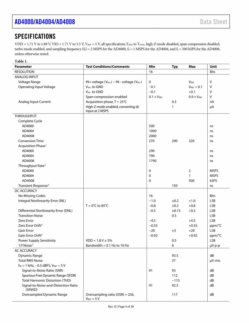
SPECIFICATIONS VDD = 1.71 V to 1.89 V, VIO = 1.71 V to 5.5 V, VREF = 5 V, all specifications TMIN to TMAX, high-Z mode disabled, span compression disabled, turbo mode enabled, and sampling frequency (fS) = 2 MSPS for the AD4000, fS = 1 MSPS for the AD4004, and fS = 500 kSPS for the AD4008, unless otherwise noted.
Table 1. Parameter Test Conditions/Comments Min Typ Max Unit RESOLUTION 16 Bits ANALOG INPUT
Voltage Range IN+ voltage (VIN+) − IN− voltage (VIN−) 0 VREF V Operating Input Voltage VIN+ to GND −0.1 VREF + 0.1 V VIN− to GND −0.1 +0.1 V Span compression enabled 0.1 × VREF 0.9 × VREF V Analog Input Current Acquisition phase, T = 25°C 0.3 nA High-Z mode enabled, converting dc
input at 2 MSPS 1 µA
THROUGHPUT Complete Cycle
AD4000 500 ns AD4004 1000 ns AD4008 2000 ns
Conversion Time 270 290 320 ns Acquisition Phase1
AD4000 290 ns AD4004 790 ns AD4008 1790 ns
Throughput Rate2 AD4000 0 2 MSPS AD4004 0 1 MSPS AD4008 0 500 kSPS
Transient Response3 150 ns DC ACCURACY
No Missing Codes 16 Bits Integral Nonlinearity Error (INL) −1.0 ±0.2 +1.0 LSB T = 0°C to 85°C −0.8 ±0.2 +0.8 LSB Differential Nonlinearity Error (DNL) −0.5 ±0.15 +0.5 LSB Transition Noise 0.5 LSB Zero Error −4.5 +4.5 LSB Zero Error Drift4 −0.55 +0.55 ppm/°C Gain Error −20 ±3 +20 LSB Gain Error Drift4 −0.92 +0.92 ppm/°C Power Supply Sensitivity VDD = 1.8 V ± 5% 0.5 LSB 1/f Noise5 Bandwidth = 0.1 Hz to 10 Hz 6 µV p-p
AC ACCURACY Dynamic Range 93.5 dB Total RMS Noise 37 µV rms fIN = 1 kHz, −0.5 dBFS, VREF = 5 V
Signal-to-Noise Ratio (SNR) 91 93 dB Spurious-Free Dynamic Range (SFDR) 112 dB Total Harmonic Distortion (THD) −115 dB Signal-to-Noise-and-Distortion Ratio
(SINAD) 91 92.5 dB
Oversampled Dynamic Range Oversampling ratio (OSR) = 256, VREF = 5 V
117 dB
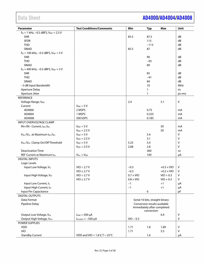
Data Sheet AD4000/AD4004/AD4008
Rev. D | Page 5 of 38
Parameter Test Conditions/Comments Min Typ Max Unit fIN = 1 kHz, −0.5 dBFS, VREF = 2.5 V
SNR 85.5 87.5 dB SFDR 115 dB THD −113 dB SINAD 85.5 87 dB
fIN = 100 kHz, −0.5 dBFS, VREF = 5 V SNR 90 dB THD −95 dB SINAD 89 dB
fIN = 400 kHz, −0.5 dBFS, VREF = 5 V SNR 85 dB THD −91 dB SINAD 84 dB
−3 dB Input Bandwidth 10 MHz Aperture Delay 1 ns Aperture Jitter 1 ps rms
REFERENCE Voltage Range, VREF 2.4 5.1 V Current VREF = 5 V
AD4000 2 MSPS 0.75 mA AD4004 1 MSPS 0.325 mA AD4008 500 kSPS 0.185 mA
INPUT OVERVOLTAGE CLAMP IN+/IN− Current, IIN+/IIN− VREF = 5 V 50 mA VREF = 2.5 V 50 mA VIN+/VIN− at Maximum IIN+/IIN− VREF = 5 V 5.4 V VREF = 2.5 V 3.1 V VIN+/VIN− Clamp On/Off Threshold VREF = 5 V 5.25 5.4 V VREF = 2.5 V 2.68 2.8 V Deactivation Time 360 ns REF Current at Maximum IIN+ VIN+ > VREF 100 µA
DIGITAL INPUTS Logic Levels
Input Low Voltage, VIL VIO > 2.7 V −0.3 +0.3 × VIO V VIO ≤ 2.7 V −0.3 +0.2 × VIO V
Input High Voltage, VIH VIO > 2.7 V 0.7 × VIO VIO + 0.3 V VIO ≤ 2.7 V 0.8 × VIO VIO + 0.3 V Input Low Current, IIL −1 +1 µA Input High Current, IIH −1 +1 µA
Input Pin Capacitance 6 pF DIGITAL OUTPUTS
Data Format Serial 16 bits, straight binary Pipeline Delay Conversion results available
immediately after completed conversion
Output Low Voltage, VOL ISINK = 500 µA 0.4 V Output High Voltage, VOH ISOURCE = −500 µA VIO − 0.3 V
POWER SUPPLIES VDD 1.71 1.8 1.89 V VIO 1.71 5.5 V Standby Current VDD and VIO = 1.8 V, T = 25°C 1.6 µA
AD4000/AD4004/AD4008 Data Sheet
Rev. D | Page 6 of 38
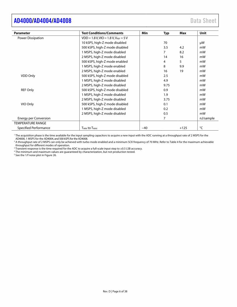
Parameter Test Conditions/Comments Min Typ Max Unit Power Dissipation VDD = 1.8 V, VIO = 1.8 V, VREF = 5 V 10 kSPS, high-Z mode disabled 70 µW 500 kSPS, high-Z mode disabled 3.5 4.2 mW 1 MSPS, high-Z mode disabled 7 8.2 mW 2 MSPS, high-Z mode disabled 14 16 mW 500 kSPS, high-Z mode enabled 4 5 mW 1 MSPS, high-Z mode enabled 8 9.9 mW 2 MSPS, high-Z mode enabled 16 19 mW
VDD Only 500 kSPS, high-Z mode disabled 2.5 mW 1 MSPS, high-Z mode disabled 4.9 mW 2 MSPS, high-Z mode disabled 9.75 mW REF Only 500 kSPS, high-Z mode disabled 0.9 mW 1 MSPS, high-Z mode disabled 1.9 mW 2 MSPS, high-Z mode disabled 3.75 mW VIO Only 500 kSPS, high-Z mode disabled 0.1 mW 1 MSPS, high-Z mode disabled 0.2 mW 2 MSPS, high-Z mode disabled 0.5 mW
Energy per Conversion 7 nJ/sample TEMPERATURE RANGE
Specified Performance TMIN to TMAX −40 +125 °C 1 The acquisition phase is the time available for the input sampling capacitors to acquire a new input with the ADC running at a throughput rate of 2 MSPS for the
AD4000, 1 MSPS for the AD4004, and 500 kSPS for the AD4008. 2 A throughput rate of 2 MSPS can only be achieved with turbo mode enabled and a minimum SCK frequency of 70 MHz. Refer to Table 4 for the maximum achievable
throughput for different modes of operation. 3 Transient response is the time required for the ADC to acquire a full-scale input step to ±0.5 LSB accuracy. 4 The minimum and maximum values are guaranteed by characterization, but not production tested. 5 See the 1/f noise plot in Figure 26.

Data Sheet AD4000/AD4004/AD4008
Rev. D | Page 7 of 38
TIMING SPECIFICATIONS VDD = 1.71 V to 1.89 V, VIO = 1.71 V to 5.5 V, VREF = 5 V, all specifications TMIN to TMAX, high-Z mode disabled, span compression disabled, turbo mode enabled, and fS = 2 MSPS for the AD4000, fS = 1 MSPS for the AD4004, and fS = 500 kSPS for the AD4008, unless otherwise noted. See Figure 3 for the timing voltage levels.
Table 2. Digital Interface Timing Parameter Symbol Min Typ Max Unit CONVERSION TIME—CNV RISING EDGE TO DATA AVAILABLE tCONV 270 290 320 ns ACQUISITION PHASE1 tACQ
AD4000 290 ns AD4004 790 ns AD4008 1790 ns
TIME BETWEEN CONVERSIONS tCYC AD4000 500 ns AD4004 1000 ns AD4008 2000 ns
CNV PULSE WIDTH (CS MODE)2 tCNVH 10 ns
SCK PERIOD (CS MODE)3 tSCK
VIO > 2.7 V 9.8 ns VIO > 1.7 V 12.3 ns
SCK PERIOD (DAISY-CHAIN MODE)4 tSCK VIO > 2.7 V 20 ns VIO > 1.7 V 25 ns
SCK LOW TIME tSCKL 3 ns SCK HIGH TIME tSCKH 3 ns SCK FALLING EDGE TO DATA REMAINS VALID DELAY tHSDO 1.5 ns SCK FALLING EDGE TO DATA VALID DELAY tDSDO
VIO > 2.7 V 7.5 ns VIO > 1.7 V 10.5 ns
CNV OR SDI LOW TO SDO D15 MOST SIGNIFICANT BIT (MSB) VALID DELAY (CS MODE) tEN
VIO > 2.7 V 10 ns VIO > 1.7 V 13 ns
CNV RISING EDGE TO FIRST SCK RISING EDGE DELAY tQUIET1 190 ns LAST SCK FALLING EDGE TO CNV RISING EDGE DELAY5 tQUIET2 60 ns CNV OR SDI HIGH OR LAST SCK FALLING EDGE TO SDO HIGH IMPEDANCE (CS MODE) tDIS 20 ns
SDI VALID SETUP TIME FROM CNV RISING EDGE tSSDICNV 2 ns SDI VALID HOLD TIME FROM CNV RISING EDGE (CS MODE) tHSDICNV 2 ns
SCK VALID HOLD TIME FROM CNV RISING EDGE (DAISY-CHAIN MODE) tHSCKCNV 12 ns SDI VALID SETUP TIME FROM SCK RISING EDGE (DAISY-CHAIN MODE) tSSDISCK 2 ns SDI VALID HOLD TIME FROM SCK RISING EDGE (DAISY-CHAIN MODE) tHSDISCK 2 ns 1 The acquisition phase is the time available for the input sampling capacitors to acquire a new input with the ADC running at a throughput rate of 2 MSPS for the
AD4000, 1 MSPS for the AD4004, and 500 kSPS for the AD4008. 2 For turbo mode, tCNVH must match the tQUIET1 minimum. 3 A throughput rate of 2 MSPS can only be achieved with turbo mode enabled and a minimum SCK frequency of 70 MHz. Refer to Table 4 for the maximum achievable
throughput for different modes of operation. See the Serial Clock Frequency Requirements section for guidelines on determining the minimum SCK rate required for a given throughput.
4 A 50% duty cycle is assumed for SCK. 5 See Figure 25 for SINAD, SNR, and ENOB vs. tQUIET2.
AD4000/AD4004/AD4008 Data Sheet
Rev. D | Page 8 of 38
Table 3. Register Read/Write Timing Parameter Symbol Min Typ Max Unit READ/WRITE OPERATION
CNV Pulse Width1 tCNVH 10 ns SCK Period tSCK
VIO > 2.7 V 9.8 ns VIO > 1.7 V 12.3 ns
SCK Low Time tSCKL 3 ns SCK High Time tSCKH 3 ns
READ OPERATION CNV Low to SDO D15 MSB Valid Delay tEN
VIO > 2.7 V 10 ns VIO > 1.7 V 13 ns
SCK Falling Edge to Data Remains Valid tHSDO 1.5 ns SCK Falling Edge to Data Valid Delay tDSDO
VIO > 2.7 V 7.5 ns VIO > 1.7 V 10.5 ns
CNV Rising Edge to SDO High Impedance tDIS 20 ns
WRITE OPERATION SDI Valid Setup Time from SCK Rising Edge tSSDISCK 2 ns SDI Valid Hold Time from SCK Rising Edge tHSDISCK 2 ns CNV Rising Edge to SCK Edge Hold Time tHCNVSCK 0 ns CNV Falling Edge to SCK Active Edge Setup Time tSCNVSCK 6 ns
1 For turbo mode, tCNVH must match the tQUIET1 minimum.
Table 4. Achievable Throughput for Different Modes of Operation Parameter Test Conditions/Comments Min Typ Max Unit THROUGHPUT, CS MODE
3-Wire and 4-Wire Turbo Mode fSCK = 100 MHz, VIO ≥ 2.7 V 2 MSPS fSCK = 80 MHz, VIO < 2.7 V 2 MSPS 3-Wire and 4-Wire Turbo Mode and Six Status Bits fSCK = 100 MHz, VIO ≥ 2.7 V 2 MSPS fSCK = 80 MHz, VIO < 2.7 V 1.86 MSPS 3-Wire and 4-Wire Mode fSCK = 100 MHz, VIO ≥ 2.7 V 1.82 MSPS fSCK = 80 MHz, VIO < 2.7 V 1.69 MSPS 3-Wire and 4-Wire Mode and Six Status Bits fSCK = 100 MHz, VIO ≥ 2.7 V 1.64 MSPS fSCK = 80 MHz, VIO < 2.7 V 1.5 MSPS
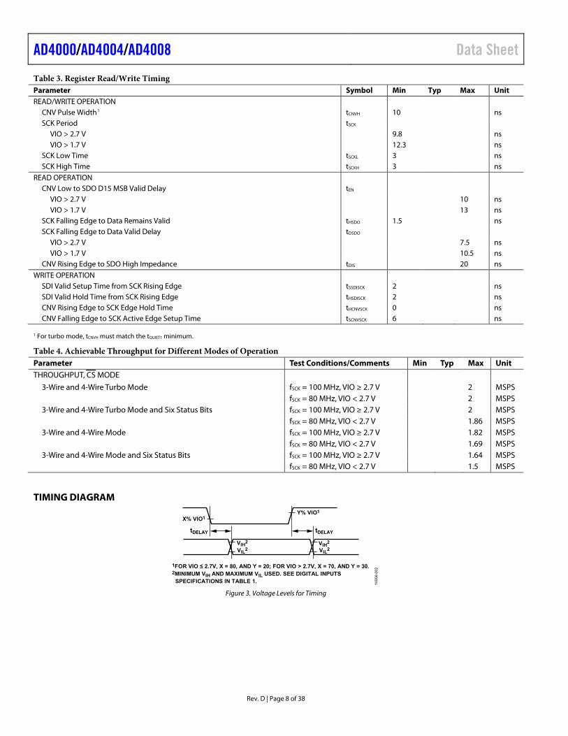
TIMING DIAGRAM
X% VIO1Y% VIO1
VIH2
VIL2VIL2VIH2
tDELAY tDELAY
1FOR VIO ≤ 2.7V, X = 80, AND Y = 20; FOR VIO > 2.7V, X = 70, AND Y = 30.2MINIMUM VIH AND MAXIMUM VIL USED. SEE DIGITAL INPUTS
SPECIFICATIONS IN TABLE 1. 1495
6-00
2
Figure 3. Voltage Levels for Timing
Data Sheet AD4000/AD4004/AD4008
Rev. D | Page 9 of 38
ABSOLUTE MAXIMUM RATINGS Note that the input overvoltage clamp cannot sustain the overvoltage condition for an indefinite amount of time.
Table 5. Parameter Rating Analog Inputs
IN+, IN− to GND1 −0.3 V to VREF + 0.4 V or ±130 mA2
Supply Voltage REF, VIO to GND −0.3 V to +6.0 V VDD to GND −0.3 V to +2.1 V VDD to VIO −6 V to +2.4 V
Digital Inputs to GND −0.3 V to VIO + 0.3 V Digital Outputs to GND −0.3 V to VIO + 0.3 V Storage Temperature Range −65°C to +150°C Junction Temperature 150°C Lead Temperature Soldering 260°C reflow as per
JEDEC J-STD-020 ESD Ratings
Human Body Model 4 kV Machine Model 200 V Field Induced Charged Device Model 1.25 kV
1 See the Analog Inputs section for an explanation of IN+ and IN−. 2 Current condition tested over a 10 ms time interval.
Stresses at or above those listed under Absolute Maximum Ratings may cause permanent damage to the product. This is a stress rating only; functional operation of the product at these or any other conditions above those indicated in the operational section of this specification is not implied. Operation beyond the maximum operating conditions for extended periods may affect product reliability.
THERMAL RESISTANCE Thermal performance is directly linked to printed circuit board (PCB) design and operating environment. Careful attention to PCB thermal design is required.
Table 6. Thermal Resistance Package Type1 θJA
2 θJC3 Unit
RM-10 147 38 °C/W CP-10-9 114 33 °C/W
1 Test Condition 1: thermal impedance simulated values are based upon use of 2S2P JEDEC PCB. See the Ordering Guide.
2 θJA is the natural convection junction-to-ambient thermal resistance measured in a one cubic foot sealed enclosure.
3 θJC is the junction-to-case thermal resistance.
ESD CAUTION
AD4000/AD4004/AD4008 Data Sheet
Rev. D | Page 10 of 38
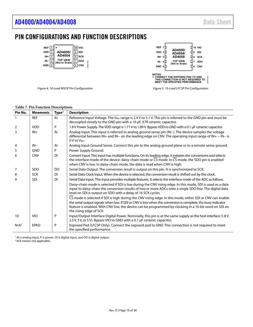
PIN CONFIGURATIONS AND FUNCTION DESCRIPTIONS REF 1
VDD 2
IN+ 3
IN– 4
GND 5
VIO10
SDI9
SCK8
SDO7
CNV6
149
56-0
03
AD4000/AD4004TOP VIEW
(Not to Scale)
Figure 4. 10-Lead MSOP Pin Configuration
1REF
2VDD
3IN+
4IN–
5GND
10 VIO
9 SDI
8 SCK
7 SDO
6 CNV
AD4000/AD4004/AD4008TOP VIEW
(Not to Scale)
14
95
6-0
04
NOTES1. CONNECT THE EXPOSED PAD TO GND.
THIS CONNECTION IS NOT REQUIRED TOMEET THE SPECIFIED PERFORMANCE.
Figure 5. 10-Lead LFCSP Pin Configuration
Table 7. Pin Function Descriptions Pin No. Mnemonic Type1 Description 1 REF AI Reference Input Voltage. The VREF range is 2.4 V to 5.1 V. This pin is referred to the GND pin and must be
decoupled closely to the GND pin with a 10 μF, X7R ceramic capacitor. 2 VDD P 1.8 V Power Supply. The VDD range is 1.71 V to 1.89 V. Bypass VDD to GND with a 0.1 μF ceramic capacitor. 3 IN+ AI Analog Input. This input is referred to analog ground sense pin (IN−). The device samples the voltage
differential between IN+ and IN− on the leading edge on CNV. The operating input range of IN+ − IN− is 0 V to VREF.
4 IN− AI Analog Input Ground Sense. Connect this pin to the analog ground plane or to a remote sense ground. 5 GND P Power Supply Ground. 6 CNV DI Convert Input. This input has multiple functions. On its leading edge, it initiates the conversions and selects
the interface mode of the device: daisy-chain mode or CS mode. In CS mode, the SDO pin is enabled when CNV is low. In daisy-chain mode, the data is read when CNV is high.
7 SDO DO Serial Data Output. The conversion result is output on this pin. It is synchronized to SCK. 8 SCK DI Serial Data Clock Input. When the device is selected, the conversion result is shifted out by this clock. 9 SDI DI Serial Data Input. This input provides multiple features. It selects the interface mode of the ADC as follows. Daisy-chain mode is selected if SDI is low during the CNV rising edge. In this mode, SDI is used as a data
input to daisy-chain the conversion results of two or more ADCs onto a single SDO line. The digital data level on SDI is output on SDO with a delay of 16 SCK cycles.
CS mode is selected if SDI is high during the CNV rising edge. In this mode, either SDI or CNV can enable the serial output signals when low. If SDI or CNV is low when the conversion is complete, the busy indicator feature is enabled. With CNV low, the device can be programmed by clocking in a 16-bit word on SDI on the rising edge of SCK.
10 VIO P Input/Output Interface Digital Power. Nominally, this pin is at the same supply as the host interface (1.8 V, 2.5 V, 3 V, or 5 V). Bypass VIO to GND with a 0.1 μF ceramic capacitor.
N/A2 EPAD P Exposed Pad (LFCSP Only). Connect the exposed pad to GND. This connection is not required to meet the specified performance.
1 AI is analog input, P is power, DI is digital input, and DO is digital output. 2 N/A means not applicable.

Data Sheet AD4000/AD4004/AD4008
Rev. D | Page 11 of 38
TYPICAL PERFORMANCE CHARACTERISTICS VDD = 1.71 V to 1.89 V, VIO = 1.71 V to 5.5 V, VREF = 5 V, all specifications TMIN to TMAX, high-Z mode disabled, span compression disabled, turbo mode enabled, and fS = 2 MSPS for the AD4000, fS = 1 MSPS for the AD4004, and fS = 500 kSPS for the AD4008, unless otherwise noted.
0 65536CODE
0.5
–0.5
INL
(LSB
)
–0.4
–0.3
–0.2
–0.1
0
0.1
0.2
0.3
0.4
8192 16384 24576 32768 40960 49152 57344
+125°C+25°C–40°C
1495
6-20
0
Figure 6. INL vs. Code for Various Temperatures, VREF = 5 V
0.3
–0.3
INL
(LSB
)
–0.2
–0.1
0
0.1
0.2
0 65536CODE
8192 16384 24576 32768 40960 49152 57344
+125°C+25°C–40°C
1495
6-20
1
Figure 7. INL vs. Code for Various Temperatures, VREF = 2.5 V
0.4
–0.4
INL
(LSB
)
–0.3
–0.2
–0.1
0
0.1
0.2
0.3
0 65536CODE
8192 16384 24576 32768 40960 49152 57344
1495
6-20
2
SPAN COMPRESSION ENABLEDHIGH-Z ENABLED
Figure 8. INL vs. Code, High-Z and Span Compression Modes,
VREF = 5 V
0.20
–0.20
DN
L (L
SB)
0 65536CODE
8192 16384 24576 32768 40960 49152 57344
+125°C+25°C–40°C
–0.15
–0.10
–0.05
0
0.05
0.10
0.15
1495
6-20
3
Figure 9. DNL vs. Code for Various Temperatures, VREF = 5 V
0.20
–0.20
DN
L (L
SB)
0 65536CODE
8192 16384 24576 32768 40960 49152 57344
+125°C+25°C–40°C
–0.15
–0.10
–0.05
0
0.05
0.10
0.15
1495
6-20
4
Figure 10. DNL vs. Code for Various Temperatures, VREF = 2.5 V
0.20
–0.20
DN
L (L
SB)
0 65536CODE
8192 16384 24576 32768 40960 49152 57344
–0.15
–0.10
–0.05
0
0.05
0.10
0.15
1495
6-20
5
SPAN COMPRESSION ENABLEDHIGH-Z ENABLED
Figure 11. DNL vs. Code, High-Z and Span Compression Modes,
VREF = 5 V
AD4000/AD4004/AD4008 Data Sheet
Rev. D | Page 12 of 38
50000
0
3276
0
3278
0
CO
DE
CO
UN
T
ADC CODE
5000
10000
15000
20000
25000
30000
35000
40000
45000
3276
132
762
3276
332
764
3276
532
766
3276
732
768
3276
932
770
3277
132
772
3277
332
774
3277
532
776
3277
732
778
3277
9
VREF = 2.5VVREF = 5V
1495
6-20
6
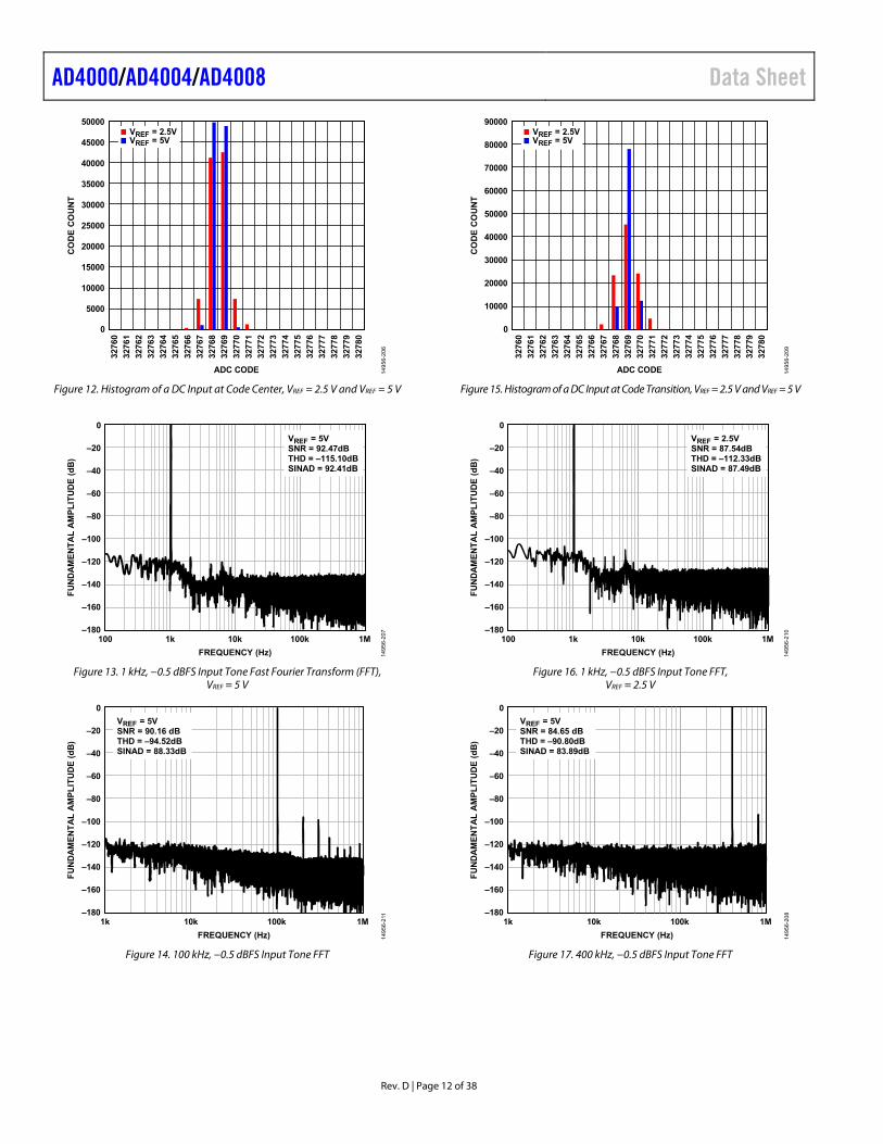
Figure 12. Histogram of a DC Input at Code Center, VREF = 2.5 V and VREF = 5 V
0
–180100 1k 10k 100k 1M
FUN
DA
MEN
TAL
AM
PLIT
UD
E (d
B)
FREQUENCY (Hz)
–160
–140
–120
–100
–80
–60
–40
–20VREF = 5VSNR = 92.47dBTHD = –115.10dBSINAD = 92.41dB
1495
6-20
7
Figure 13. 1 kHz, −0.5 dBFS Input Tone Fast Fourier Transform (FFT),
VREF = 5 V
0
–1801k 10k 100k 1M
FUN
DA
MEN
TAL
AM
PLIT
UD
E (d
B)
FREQUENCY (Hz)
–160
–140
–120
–100
–80
–60
–40
–20VREF = 5VSNR = 90.16 dBTHD = –94.52dBSINAD = 88.33dB
1495
6-21
1
Figure 14. 100 kHz, −0.5 dBFS Input Tone FFT
90000
0
3276
0
3278
0
CO
DE
CO
UN
T
ADC CODE
3276
132
762
3276
332
764
3276
532
766
3276
732
768
3276
932
770
3277
132
772
3277
332
774
3277
532
776
3277
732
778
3277
9
VREF = 2.5VVREF = 5V
10000
20000
30000
40000
50000
60000
70000
80000
1495
6-20
9
Figure 15. Histogram of a DC Input at Code Transition, VREF = 2.5 V and VREF = 5 V
0
–180100 1k 10k 100k 1M
FUN
DA
MEN
TAL
AM
PLIT
UD
E (d
B)
FREQUENCY (Hz)
–160
–140
–120
–100
–80
–60
–40
–20VREF = 2.5VSNR = 87.54dBTHD = –112.33dBSINAD = 87.49dB
1495
6-21
0
Figure 16. 1 kHz, −0.5 dBFS Input Tone FFT,
VREF = 2.5 V
0
–1801k 10k 100k 1M
FUN
DA
MEN
TAL
AM
PLIT
UD
E (d
B)
FREQUENCY (Hz)
–160
–140
–120
–100
–80
–60
–40
–20VREF = 5VSNR = 84.65 dBTHD = –90.80dBSINAD = 83.89dB
1495
6-20
8
Figure 17. 400 kHz, −0.5 dBFS Input Tone FFT
Data Sheet AD4000/AD4004/AD4008
Rev. D | Page 13 of 38
94
801k 10k 100k 1M
SNR
, SIN
AD
(dB
)
INPUT FREQUENCY (Hz)
15.2
13.2
ENO
B (B
its)
82
84
86
88
90
92
13.4
13.6
13.8
14.0
14.2
14.4
14.6
14.8
15.0ENOBSINADSNR
1495
6-21
2
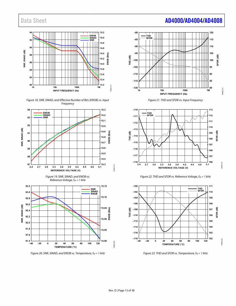
Figure 18. SNR, SINAD, and Effective Number of Bits (ENOB) vs. Input Frequency
94
93
92
91
90
89
88
87
SNR
, SIN
AD
(dB
)
2.4 2.7 3.0 3.3 3.6 3.9 4.2 4.5 4.8 5.1REFERENCE VOLTAGE (V)
15.3
14.3
ENO
B (B
its)
14.4
14.5
14.6
14.7
14.8
14.9
15.0
15.1
15.2ENOBSINADSNR
1495
6-21
3
Figure 19. SNR, SINAD, and ENOB vs. Reference Voltage, fIN = 1 kHz
SNR
, SIN
AD
(dB
)
TEMPERATURE (°C)
14.90
14.95
15.00
15.05
15.10
15.15
91.4
91.6
91.8
92.0
92.2
92.4
92.6
92.8
93.0
93.2
ENO
B (B
its)
–40 –20 0 4020 60 80 100 120
SNRSINADENOB
1495
6-22
0
Figure 20. SNR, SINAD, and ENOB vs. Temperature, fIN = 1 kHz
–80
–120
–110
–115
–105
–95
–85
–100
–90
1k 10k 100k 1M
THD
(dB
)
INPUT FREQUENCY (Hz)
80
120
SFD
R (d
B)
85
90
95
100
105
110
115THDSFDR
1495
6-21
5
Figure 21. THD and SFDR vs. Input Frequency
–110
–1182.4 5.1
THD
(dB)
REFERENCE VOLTAGE (V)
THDSFDR
–117
–116
–115
–114
–113
–112
–111
2.7 3.0 3.3 3.6 3.9 4.2 4.5 4.8
113
106
107
108
107
108
109
110
111
112
SFDR
(dB)
1495
6-21
6
Figure 22. THD and SFDR vs. Reference Voltage, fIN = 1 kHz
THD
(dB)
TEMPERATURE (°C)
SFDR
(dB)
–40 –20 0 4020 60 80 100 120102
103
104
105
106
107
108
109
110
111
–118
–116
–114
–112
–110
–108
–106
–104
–102
–100THDSFDR
1495
6-22
2
Figure 23. THD and SFDR vs. Temperature, fIN = 1 kHz

AD4000/AD4004/AD4008 Data Sheet
Rev. D | Page 14 of 38
14
95
6-2
1490
95
100
105
110
115
120
125
1 2 4 8 16 32 64 128 256 512 1024 2048
SN
R (
dB
)
DECIMATION RATE
DYNAMIC RANGEfIN = 1kHzfIN = 10kHz
Figure 24. SNR vs. Decimation Rate for Various Input Frequencies, 2 MSPS
93.4
92.00 10 20 30 40 50 60 70
SN
R,
SIN
AD
(d
B)
tQUIET2 (ns)
ENOBSINADSNR
92.2
92.4
92.6
92.8
93.0
93.2
15.25
14.95
EN
OB
(B
its)
15.00
15.05
15.10
15.15
15.20
149
56-
217
Figure 25. SNR, SINAD, and ENOB vs. tQUIET2
AD
C O
UT
PU
T R
EA
DIN
G (
µV
)
TIME (Seconds)
0 2 4 6 8 10948
949
950
951
952
953
954
955
149
56-2
18
Figure 26. 1/f Noise for 0.1 Hz to 10 Hz Bandwidth, 50 kSPS, 2500 Samples Averaged per Reading
1 2 105 20 50
TH
D (
dB
)
INPUT FREQUENCY (kHz)
–115
–110
–105
–100
–95
–90
–85
–80
–75
14
95
6-2
25
500Ω HIGH-Z OFF500Ω HIGH-Z ON1000Ω HIGH-Z OFF1000Ω HIGH-Z ON
200Ω HIGH-Z OFF200Ω HIGH-Z ON
Figure 27. THD vs. Input Frequency for Various Source Impedances
ZE
RO
ER
RO
R A
ND
GA
IN E
RR
OR
(L
SB
)
TEMPERATURE (°C)
–40 –20 0 4020 60 80 100 120–1.0
–0.8
–0.6
–0.4
–0.2
0
0.2
0.4
0.6
0.8
1.0ZERO ERRORGAIN ERROR
14
95
6-2
23
Figure 28. Zero Error and Gain Error vs. Temperature
1495
6-2
21
–25
–20
–15
–10
–5
0
5
10
15
20
25
0 0.5 1.0 1.5 2.0 2.5 3.0 3.5 4.0 4.5 5.0
INP
UT
CU
RR
EN
T (μ
A)
INPUT DIFFERENTIAL VOLTAGE (V)
HIGH-Z DISABLED, 2MSPSHIGH-Z DISABLED, 1MSPSHIGH-Z DISABLED, 500kSPSHIGH-Z ENABLED, 2MSPSHIGH-Z ENABLED, 1MSPSHIGH-Z ENABLED, 500kSPS
Figure 29. Analog Input Current vs. Input Differential Voltage

Data Sheet AD4000/AD4004/AD4008
Rev. D | Page 15 of 38
–40 –20 0 4020 60 80 100 120
TEMPERATURE (°C)
OP
ER
AT
ING
CU
RR
EN
T (
mA
)
VDD HIGH-Z ENABLEDVDD HIGH-Z DISABLEDREF HIGH-Z ENABLEDREF HIGH-Z DISABLEDVIO HIGH-Z ENABLEDVIO HIGH-Z DISABLED
0
1
2
3
4
5
6
7
8
14
95
6-2
26
Figure 30. Operating Current vs. Temperature, AD4000, 2 MSPS
0
0.5
1.0
1.5
2.0
2.5
3.0
3.5
–40 –20 0 20 40 60 80 100 120
OP
ER
AT
ING
CU
RR
EN
T (
mA
)
TEMPERATURE (°C) 14
95
6-2
32
VDD HIGH-Z ENABLEDVDD HIGH-Z DISABLEDREF HIGH-Z ENABLEDREF HIGH-Z DISABLEDVIO HIGH-Z ENABLEDVIO HIGH-Z DISABLED
Figure 31. Operating Current vs. Temperature, AD4004, 1 MSPS
–40 –20 0 4020 60 80 100 120
TEMPERATURE (°C)
OP
ER
AT
ING
CU
RR
EN
T (
mA
)
0
149
56-3
25
0.2
0.4
0.6
0.8
1.0
1.2
1.4
1.6
1.8
2.0
VDD HIGH-Z ENABLEDVDD HIGH-Z DISABLEDREF HIGH-Z ENABLEDREF HIGH-Z DISABLEDVIO HIGH-Z ENABLEDVIO HIGH-Z DISABLED
Figure 32. Operating Current vs. Temperature, AD4008, 500 kSPS
100 1k 10k 100k 1M
PS
RR
(d
B)
FREQUENCY (Hz)
55
60
65
70
75
80
149
56-2
30
Figure 33. PSRR vs. Frequency
14
956
-2192.4 2.7 3.0 3.3 3.6 3.9 4.2 4.5 4.8 5.1
RE
FE
RE
NC
E C
UR
RE
NT
(m
A)
REFERENCE VOLTAGE (V)
0
0.1
0.2
0.3
0.4
0.5
0.6
0.7
0.8
2MSPS1MSPS500kSPS
Figure 34. Reference Current vs. Reference Voltage
10 100 1k 10k 100k 1M 2M
PO
WE
R D
ISS
IPA
TIO
N (
µW
)
THROUGHPUT (SPS)
0.01
0.1
1
10
100
1k
10k
100kVDDVIOREFTOTAL POWER
1495
6-22
7
POWER DISSIPATIONMEASUREMENTS APPLY TOEACH PRODUCT OVER ITSSPECIFIED THROUGHPUT RANGE.
Figure 35. Power Dissipation vs. Throughput
AD4000/AD4004/AD4008 Data Sheet
Rev. D | Page 16 of 38
–40 –20 0 4020 60 80 100 120
STA
ND
BY
CU
RR
ENT
(µA
)
TEMPERATURE (°C)
0
2
4
6
8
10
1
3
5
7
9
11
12
1495
6-22
4
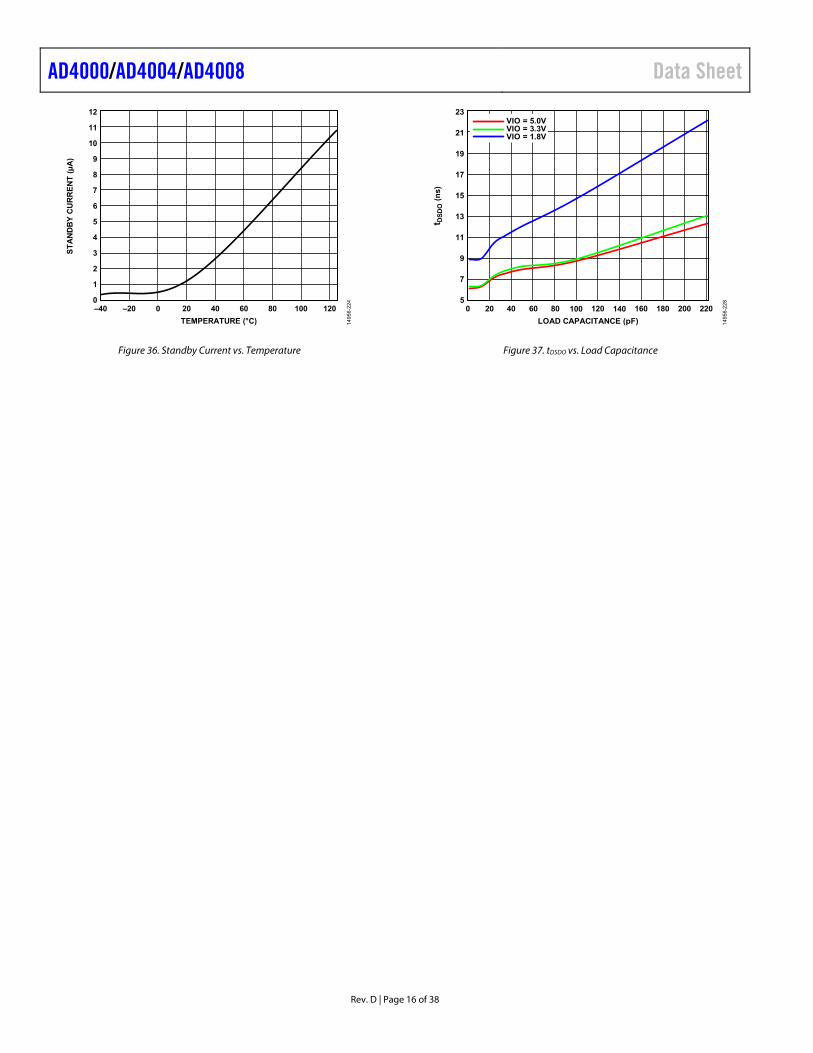
Figure 36. Standby Current vs. Temperature
0 20 40 60 80 100 120 140 160 180 200 220
t DSD
O (n
s)
LOAD CAPACITANCE (pF)
5
7
9
11
13
15
17
19
21
23VIO = 5.0VVIO = 3.3VVIO = 1.8V
1495
6-22
8
Figure 37. tDSDO vs. Load Capacitance

Data Sheet AD4000/AD4004/AD4008
Rev. D | Page 17 of 38
TERMINOLOGY Integral Nonlinearity Error (INL) INL is the deviation of each individual code from a line drawn from negative full scale through positive full scale. The point used as negative full scale occurs ½ LSB before the first code transition. Positive full scale is defined as a level 1½ LSB beyond the last code transition. The deviation is measured from the middle of each code to the true straight line (see Figure 39).
Differential Nonlinearity Error (DNL) In an ideal ADC, code transitions are 1 LSB apart. DNL is the maximum deviation from this ideal value. It is often specified in terms of resolution for which no missing codes are guaranteed.
Zero Error Zero error is the difference between the ideal voltage that results in the first code transition (½ LSB above analog ground) and the actual voltage producing that code.
Gain Error The first transition (from 100 ... 00 to 100 ... 01) occurs at a level ½ LSB above nominal negative full scale (−4.999981 V for the ±5 V range). The last transition (from 011 … 10 to 011 … 11) occurs for an analog voltage 1½ LSB below the nominal full scale (+4.999943 V for the ±5 V range). The gain error is the deviation of the difference between the actual level of the last transition and the actual level of the first transition from the difference between the ideal levels.
Spurious-Free Dynamic Range (SFDR) SFDR is the difference, in decibels (dB), between the rms amplitude of the input signal and the peak spurious signal.
Effective Number of Bits (ENOB) ENOB is a measurement of the resolution with a sine wave input. It is related to SINAD as follows:
ENOB = (SINADdB − 1.76)/6.02
ENOB is expressed in bits.
Total Harmonic Distortion (THD) THD is the ratio of the rms sum of the first five harmonic components to the rms value of a full-scale input signal and is expressed in decibels.
Dynamic Range Dynamic range is the ratio of the rms value of the full scale to the total rms noise measured. The value for dynamic range is expressed in decibels. It is measured with a signal at −60 dBFS so that it includes all noise sources and DNL artifacts.
Signal-to-Noise Ratio (SNR) SNR is the ratio of the rms value of the actual input signal to the rms sum of all other spectral components below the Nyquist frequency, excluding harmonics and dc. The value for SNR is expressed in decibels.
Signal-to-Noise-and-Distortion Ratio (SINAD) SINAD is the ratio of the rms value of the actual input signal to the rms sum of all other spectral components that are less than the Nyquist frequency, including harmonics but excluding dc. The value of SINAD is expressed in decibels.
Aperture Delay Aperture delay is the measure of the acquisition performance and is the time between the rising edge of the CNV input and when the input signal is held for a conversion.
Transient Response Transient response is the time required for the ADC to acquire a full-scale input step to ±0.5 LSB accuracy.
Power Supply Rejection Ratio (PSRR) PSRR is the ratio of the power in the ADC output at the frequency, f, to the power of a 200 mV p-p sine wave applied to the ADC VDD supply of frequency, f.
PSRR (dB) = 10 log(PVDD_IN/PADC_OUT)
where: PVDD_IN is the power at the frequency, f, at the VDD pin. PADC_OUT is the power at the frequency, f, in the ADC output.

AD4000/AD4004/AD4008 Data Sheet
Rev. D | Page 18 of 38
THEORY OF OPERATION
COMP CONTROLLOGIC
SWITCHES CONTROL
BUSY
OUTPUT CODE
CNV
CC2C16,384C 4C32,768C
LSB SW+MSB
LSB SW–MSB
CC2C16,384C 4C32,768C
IN+
REF
GND
IN– 1495
6-00
6
Figure 38. ADC Simplified Schematic
CIRCUIT INFORMATION The AD4000/AD4004/AD4008 are high speed, low power, single-supply, precise, 16-bit pseudo differential ADCs based on a SAR architecture.
The AD4000 is capable of converting 2,000,000 samples per second (2 MSPS), the AD4004 is capable of converting 1,000,000 samples per second (1 MSPS), and the AD4008 is capable of converting 500,000 samples per second (500 kSPS). The power consumption of the AD4000/AD4004/AD4008 scales with throughput because they power down in between conversions. When operating at 10 kSPS, for example, they typically consume 70 µW, making them ideal for battery-powered applications. The AD4000/AD4004/AD4008 also have a valid first conversion after being powered down for long periods, which can further reduce power consumed in applications in which the ADC does not need to be constantly converting.
The AD4000/AD4004/AD4008 provide the user with an on-chip track-and-hold and do not exhibit any pipeline delay or latency, making them ideal for multiplexed applications.
The AD4000/AD4004/AD4008 incorporate a multitude of unique ease of use features that result in a lower system power and smaller footprint.
The AD4000/AD4004/AD4008 each have an internal voltage clamp that protects the device from overvoltage damage on the analog inputs.
The analog input incorporates circuitry that reduces the nonlinear charge kickback seen from a typical switched capacitor SAR input. This reduction in kickback, combined with a longer acquisition phase, means reduced settling requirements on the driving amplifier. This combination allows the use of lower bandwidth and lower power amplifiers as drivers. It has the additional benefit of allowing a larger resistor value in the input RC filter and a corresponding smaller capacitor, which results in a smaller RC load for the amplifier, improving stability and power dissipation.
High-Z mode can be enabled via the SPI interface by programming a register bit (see Table 12). When high-Z mode is enabled,
the ADC input has a low input charging current at low input signal frequencies as well as improved distortion over a wide frequency range up to 100 kHz. For frequencies greater than 100 kHz and multiplexing, disable high-Z mode.
For single-supply applications, a span compression feature creates additional headroom and footroom for the driving amplifier to access the full range of the ADC.
The fast conversion time of the AD4000/AD4004/AD4008, along with turbo mode, allows low clock rates to read back conversions, even when running at their respective maximum throughput rates. Note that, for the AD4000, the full throughput rate of 2 MSPS can be achieved only with turbo mode enabled.
The AD4000/AD4004/AD4008 can interface with any 1.8 V to 5 V digital logic family. These devices are available in a 10-lead MSOP or a tiny 10-lead LFCSP that allows space savings and flexible configurations.
The AD4000/AD4004/AD4008 are pin for pin compatible with some of the 14-/16-/18-/20-bit precision SAR ADCs listed in Table 8.
Table 8. MSOP, LFCSP 14-/16-/18-/20-Bit Precision SAR ADCs
Bits 100 kSPS 250 kSPS 400 kSPS to 500 kSPS ≥1000 kSPS
201 AD40202 181 AD7989-12 AD76912 AD40112,
AD76902, AD7989-52
AD40032, AD40072, AD79822, AD79842
183 AD40102 AD40022, AD40062
161 AD7684 AD76872 AD76882, AD76932, AD79162
AD40012, AD40052, AD79152
163 AD7680, AD7683, AD7988-12
AD76852, AD7694
AD76862, AD7988-52, AD40082
AD40002, AD40042, AD79802, AD79832
143 AD7940 AD79422 AD79462 Not applicable 1 True differential. 2 Pin for pin compatible. 3 Pseudo differential.
Data Sheet AD4000/AD4004/AD4008
Rev. D | Page 19 of 38
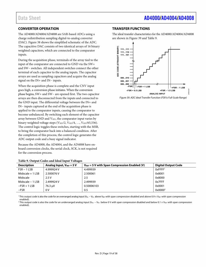
CONVERTER OPERATION The AD4000/AD4004/AD4008 are SAR-based ADCs using a charge redistribution sampling digital-to-analog converter (DAC). Figure 38 shows the simplified schematic of the ADC. The capacitive DAC consists of two identical arrays of 16 binary weighted capacitors, which are connected to the comparator inputs.
During the acquisition phase, terminals of the array tied to the input of the comparator are connected to GND via the SW+ and SW− switches. All independent switches connect the other terminal of each capacitor to the analog inputs. The capacitor arrays are used as sampling capacitors and acquire the analog signal on the IN+ and IN− inputs.
When the acquisition phase is complete and the CNV input goes high, a conversion phase initiates. When the conversion phase begins, SW+ and SW− are opened first. The two capacitor arrays are then disconnected from the inputs and connected to the GND input. The differential voltage between the IN+ and IN− inputs captured at the end of the acquisition phase is applied to the comparator inputs, causing the comparator to become unbalanced. By switching each element of the capacitor array between GND and VREF, the comparator input varies by binary weighted voltage steps (VREF/2, VREF/4, …, VREF/65,536). The control logic toggles these switches, starting with the MSB, to bring the comparator back into a balanced condition. After the completion of this process, the control logic generates the ADC output code and a busy signal indicator.
Because the AD4000, the AD4004, and the AD4008 have on-board conversion clocks, the serial clock, SCK, is not required for the conversion process.
TRANSFER FUNCTIONS The ideal transfer characteristics for the AD4000/AD4004/AD4008 are shown in Figure 39 and Table 9.
000...000
000...001
000...010
111...101111...110
111...111
AD
C C
OD
E (
ST
RA
IGH
T B
INA
RY
)
ANALOG INPUT
+FSR – 1.5 LSB
+FSR – 1 LSB–FSR + 1 LSB–FSR
–FSR + 0.5 LSB
1495
6-00
7
Figure 39. ADC Ideal Transfer Function (FSR Is Full-Scale Range)
Table 9. Output Codes and Ideal Input Voltages Description Analog Input, VREF = 5 V VREF = 5 V with Span Compression Enabled (V) Digital Output Code FSR − 1 LSB 4.999924 V 4.499939 0xFFFF1 Midscale + 1 LSB 2.500076 V 2.500061 0x8001 Midscale 2.5 V 2.5 0x8000 Midscale − 1 LSB 2.499924 V 2.499939 0x7FFF −FSR + 1 LSB 76.3 μV 0.50006103 0x0001 −FSR 0 V 0.5 0x00002 1 This output code is also the code for an overranged analog input (VIN+ − VIN− above VREF with span compression disabled and above 0.9 × VREF with span compression
enabled). 2 This output code is also the code for an underranged analog input (VIN+ − VIN− below 0 V with span compression disabled and below 0.1 × VREF with span compression
enabled).
AD4000/AD4004/AD4008 Data Sheet
Rev. D | Page 20 of 38
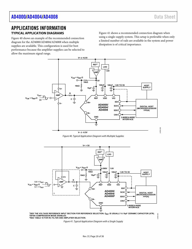
APPLICATIONS INFORMATION TYPICAL APPLICATION DIAGRAMS Figure 40 shows an example of the recommended connection diagram for the AD4000/AD4004/AD4008 when multiple supplies are available. This configuration is used for best performance because the amplifier supplies can be selected to allow the maximum signal range.
Figure 41 shows a recommended connection diagram when using a single-supply system. This setup is preferable when only a limited number of rails are available in the system and power dissipation is of critical importance.
C
R
V+
REF VDD VIO
GND
IN+
IN–
SDI
SCK
SDO
CNV
AD4000/AD4004/AD4008
3-WIRE/4-WIREINTERFACE
1.8V
1.8V TO 5V
V+ ≥ +6.5V
DIGITAL HOST(MICROPROCESSOR/
FPGA)
V– ≤ –0.5V
HOSTSUPPLY
100nF 100nF
5V
V–
AMPVREF
0VVCM = VREF/2
REF1
LDO
AMP
VCM = VREF/2
10µF10kΩ
10kΩ
14
95
6-0
08
Figure 40. Typical Application Diagram with Multiple Supplies
C
R
REF VDD VIO
GND
IN+
IN–
SDI
SCK
SDO
CNV
AD4000/AD4004/AD40082
1.8V
1.8V TO 5V
V+ = 5V
DIGITAL HOST(MICROPROCESSOR/
FPGA)
HOSTSUPPLY
100nF 100nF
4.096V
AMP0.9 × VREF
0.1 × VREF
VCM = VREF/2
REF1
LDO
AMP
VCM = VREF/2
10µF110kΩ
10kΩ
3-WIRE/4-WIREINTERFACE
1495
6-00
9
3
1SEE THE VOLTAGE REFERENCE INPUT SECTION FOR REFERENCE SELECTION. CREF IS USUALLY A 10µF CERAMIC CAPACITOR (X7R).2SPAN COMPRESSION MODE ENABLED.3SEE TABLE 10 FOR RC FILTER AND AMPLIFIER SELECTION.
Figure 41. Typical Application Diagram with a Single Supply
Data Sheet AD4000/AD4004/AD4008
Rev. D | Page 21 of 38
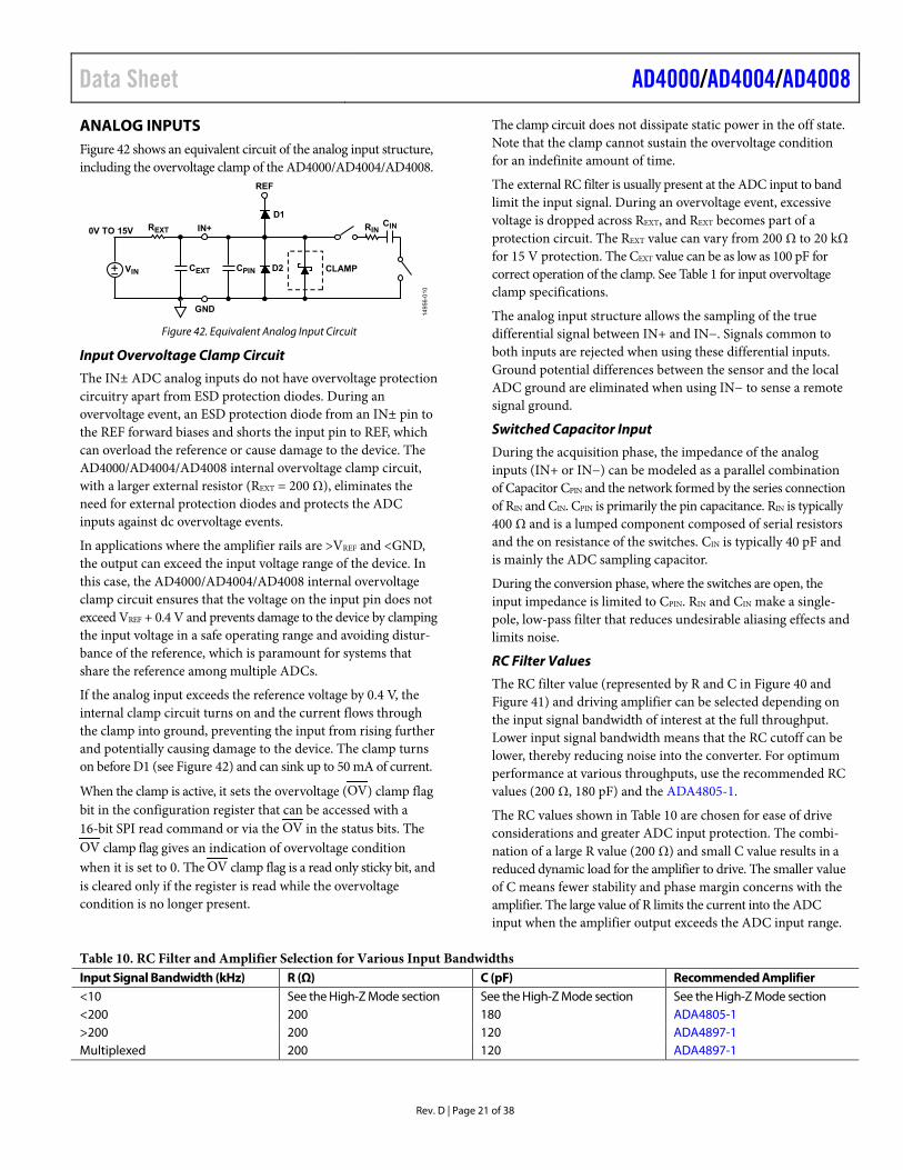
ANALOG INPUTS Figure 42 shows an equivalent circuit of the analog input structure, including the overvoltage clamp of the AD4000/AD4004/AD4008.
CEXT
REXT
VIN
REF
D1IN+
GND
CLAMP
0V TO 15V RINCIN
D2CPIN
1495
6-01
0
Figure 42. Equivalent Analog Input Circuit
Input Overvoltage Clamp Circuit
The IN± ADC analog inputs do not have overvoltage protection circuitry apart from ESD protection diodes. During an overvoltage event, an ESD protection diode from an IN± pin to the REF forward biases and shorts the input pin to REF, which can overload the reference or cause damage to the device. The AD4000/AD4004/AD4008 internal overvoltage clamp circuit, with a larger external resistor (REXT = 200 Ω), eliminates the need for external protection diodes and protects the ADC inputs against dc overvoltage events.
In applications where the amplifier rails are >VREF and <GND, the output can exceed the input voltage range of the device. In this case, the AD4000/AD4004/AD4008 internal overvoltage clamp circuit ensures that the voltage on the input pin does not exceed VREF + 0.4 V and prevents damage to the device by clamping the input voltage in a safe operating range and avoiding distur-bance of the reference, which is paramount for systems that share the reference among multiple ADCs.
If the analog input exceeds the reference voltage by 0.4 V, the internal clamp circuit turns on and the current flows through the clamp into ground, preventing the input from rising further and potentially causing damage to the device. The clamp turns on before D1 (see Figure 42) and can sink up to 50 mA of current.
When the clamp is active, it sets the overvoltage (OV) clamp flag bit in the configuration register that can be accessed with a 16-bit SPI read command or via the OV in the status bits. The OV clamp flag gives an indication of overvoltage condition when it is set to 0. The OV clamp flag is a read only sticky bit, and is cleared only if the register is read while the overvoltage condition is no longer present.
The clamp circuit does not dissipate static power in the off state. Note that the clamp cannot sustain the overvoltage condition for an indefinite amount of time.
The external RC filter is usually present at the ADC input to band limit the input signal. During an overvoltage event, excessive voltage is dropped across REXT, and REXT becomes part of a protection circuit. The REXT value can vary from 200 Ω to 20 kΩ for 15 V protection. The CEXT value can be as low as 100 pF for correct operation of the clamp. See Table 1 for input overvoltage clamp specifications.
The analog input structure allows the sampling of the true differential signal between IN+ and IN−. Signals common to both inputs are rejected when using these differential inputs. Ground potential differences between the sensor and the local ADC ground are eliminated when using IN− to sense a remote signal ground.
Switched Capacitor Input
During the acquisition phase, the impedance of the analog inputs (IN+ or IN−) can be modeled as a parallel combination of Capacitor CPIN and the network formed by the series connection of RIN and CIN. CPIN is primarily the pin capacitance. RIN is typically 400 Ω and is a lumped component composed of serial resistors and the on resistance of the switches. CIN is typically 40 pF and is mainly the ADC sampling capacitor.
During the conversion phase, where the switches are open, the input impedance is limited to CPIN. RIN and CIN make a single-pole, low-pass filter that reduces undesirable aliasing effects and limits noise.
RC Filter Values
The RC filter value (represented by R and C in Figure 40 and Figure 41) and driving amplifier can be selected depending on the input signal bandwidth of interest at the full throughput. Lower input signal bandwidth means that the RC cutoff can be lower, thereby reducing noise into the converter. For optimum performance at various throughputs, use the recommended RC values (200 Ω, 180 pF) and the ADA4805-1.
The RC values shown in Table 10 are chosen for ease of drive considerations and greater ADC input protection. The combi-nation of a large R value (200 Ω) and small C value results in a reduced dynamic load for the amplifier to drive. The smaller value of C means fewer stability and phase margin concerns with the amplifier. The large value of R limits the current into the ADC input when the amplifier output exceeds the ADC input range.
Table 10. RC Filter and Amplifier Selection for Various Input Bandwidths Input Signal Bandwidth (kHz) R (Ω) C (pF) Recommended Amplifier <10 See the High-Z Mode section See the High-Z Mode section See the High-Z Mode section <200 200 180 ADA4805-1 >200 200 120 ADA4897-1 Multiplexed 200 120 ADA4897-1
AD4000/AD4004/AD4008 Data Sheet
Rev. D | Page 22 of 38
DRIVER AMPLIFIER CHOICE Although the AD4000/AD4004/AD4008 are easy to drive, the driver amplifier must meet the following requirements:
The noise generated by the driver amplifier must be kept low enough to preserve the SNR and transition noise performance of the AD4000/AD4004/AD4008. The noise from the driver is filtered by the single-pole, low-pass filter of the analog input circuit made by RIN and CIN, or by the external filter, if one is used. Because the typical noise of the AD4000/AD4004/AD4008 is 37 μV rms, the SNR degradation due to the amplifier is
22 )(
2πμV37
μV37log20
NdB3
LOSS
NefSNR
where: f−3 dB is the input bandwidth, in megahertz, of the AD4000/ AD4004/AD4008 (10 MHz) or the cutoff frequency of the input filter, if one is used. N is the noise gain of the amplifier (for example, 1 in buffer configuration). eN is the equivalent input noise voltage of the op amp, in nV/√Hz.
For ac applications, the driver must have a THD performance commensurate with the AD4000/ AD4004/AD4008.
For multichannel multiplexed applications, the driver amplifier and the analog input circuit of the AD4000/ AD4004/AD4008 must settle for a full-scale step onto the capacitor array at a 16-bit level (0.0001525%, 15.25 ppm). In the data sheet of the amplifier, settling at 0.1% to 0.01% is more commonly specified. This settling may differ significantly from the settling time at a 16-bit level and must be verified prior to driver selection.
High Frequency Input Signals
The AD4000/AD4004/AD4008 ac performance over a wide input frequency range using a 5 V reference voltage is shown in Figure 18 and Figure 21. Unlike other traditional SAR ADCs, the AD4000/AD4004/AD4008 maintain exceptional ac performance for input frequencies up to the Nyquist frequency with minimal performance degradation. Note that the input frequency is limited to the Nyquist frequency of the sample rate in use.
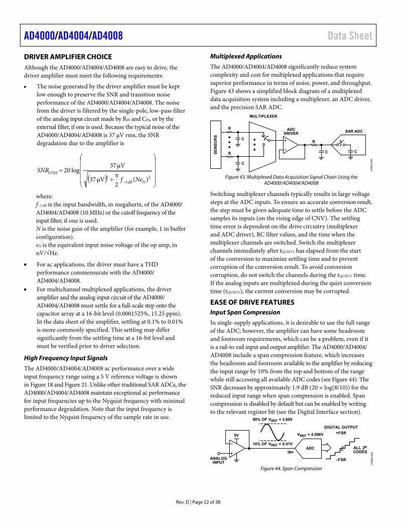
Multiplexed Applications
The AD4000/AD4004/AD4008 significantly reduce system complexity and cost for multiplexed applications that require superior performance in terms of noise, power, and throughput. Figure 43 shows a simplified block diagram of a multiplexed data acquisition system including a multiplexer, an ADC driver, and the precision SAR ADC.
SAR ADCADCDRIVER
MULTIPLEXER
SE
NS
OR
S
R
R
R C C
C
C
14
95
6-0
40
Figure 43. Multiplexed Data Acquisition Signal Chain Using the
AD4000/AD4004/AD4008
Switching multiplexer channels typically results in large voltage steps at the ADC inputs. To ensure an accurate conversion result, the step must be given adequate time to settle before the ADC samples its inputs (on the rising edge of CNV). The settling time error is dependent on the drive circuitry (multiplexer and ADC driver), RC filter values, and the time when the multiplexer channels are switched. Switch the multiplexer channels immediately after tQUIET1 has elapsed from the start of the conversion to maximize settling time and to prevent corruption of the conversion result. To avoid conversion corruption, do not switch the channels during the tQUIET1 time. If the analog inputs are multiplexed during the quiet conversion time (tQUIET1), the current conversion may be corrupted.
EASE OF DRIVE FEATURES Input Span Compression
In single-supply applications, it is desirable to use the full range of the ADC; however, the amplifier can have some headroom and footroom requirements, which can be a problem, even if it is a rail-to-rail input and output amplifier. The AD4000/AD4004/ AD4008 include a span compression feature, which increases the headroom and footroom available to the amplifier by reducing the input range by 10% from the top and bottom of the range while still accessing all available ADC codes (see Figure 44). The SNR decreases by approximately 1.9 dB (20 × log(8/10)) for the reduced input range when span compression is enabled. Span compression is disabled by default but can be enabled by writing to the relevant register bit (see the Digital Interface section).
14
95
6-3
00
ADC
VREF = 4.096V
DIGITAL OUTPUT
ALL 2N
CODES
+FSR
–FSR
90% OF VREF = 3.69V
10% OF VREF = 0.41V
ANALOGINPUT
5V
IN+
Figure 44. Span Compression

Data Sheet AD4000/AD4004/AD4008
Rev. D | Page 23 of 38
High-Z Mode The AD4000/AD4004/AD4008 incorporate high-Z mode, which reduces the nonlinear charge kickback when the capacitor DAC switches back to the input at the start of acquisition. Figure 29 shows the input current of the AD4000/AD4004/AD4008 with high-Z mode enabled and disabled. The low input current makes the ADC easier to drive than the traditional SAR ADCs, even with high-Z mode disabled. The input current reduces further to submicroampere range when high-Z mode is enabled. High-Z mode is disabled by default but can be enabled by writing to the register (see Table 12). Disable high-Z mode for input frequencies above 100 kHz or when multiplexing.
To achieve the optimal data sheet performance from traditional high resolution precision SAR ADCs, system designers are often forced to use a dedicated, high power, high speed amplifier to drive the switched capacitor SAR ADC inputs. High-Z mode allows a choice of lower power and lower bandwidth precision amplifiers with a lower RC filter cutoff to drive the ADC, removing the need for dedicated high speed ADC drivers, which saves system power, size, and cost in precision, low bandwidth appli-cations. High-Z mode allows the amplifier and RC filter in front of the ADC to be chosen based on the signal bandwidth of interest, rather than the settling requirements of the switched capacitor SAR ADC inputs. High-Z mode improves distortion performance (THD) and reduces analog input current for input signals up to 100 kHz.
The AD4000/AD4004/AD4008 can be driven with a much higher source impedance than traditional SARs, which means the resistor in the RC filter can have a value 10 × larger than previous SAR designs and can tolerate larger impedance with high-Z mode enabled. Figure 27 shows the THD performance for various source impedances with high-Z mode disabled and enabled.
Figure 45 and Figure 46 show the AD4000/AD4004/AD4008 SNR and THD performance using the ADA4077-1 (supply current per amplifier (ISY) = 400 μA) and ADA4610-1 (ISY = 1.50 mA) precision amplifiers when driving the AD4000/AD4004/ AD4008 at full throughput for high-Z mode both enabled and disabled with various RC filter values. These amplifiers achieve 91 dB to 92 dB typical SNR and close to −100 dB typical THD with high-Z enabled for a 2.27 MHz RC bandwidth. The THD is improved by ~ 5 dB with high-Z mode enabled, even for large R values greater than 200 Ω. SNR maintains close to 85 dB, even with a very low RC filter cutoff.
When high-Z mode is enabled, the ADC consumes approximately 1 mW per MSPS of extra power; however, this is still significantly lower than using dedicated ADC drivers like the ADA4807-1. For any system, the front end typically limits the overall ac/dc performance of the signal chain. The data sheets of the selected precision amplifiers, shown in Figure 45 and Figure 46, show that their own noise and distortion performance dominates the SNR and THD specification at a certain input frequency.
SN
R (
dB
)
70
80
75
85
90
95
260.482kHz1.3kΩ470pF
497.981kHz680Ω470pF
1.3MHz680Ω180pF
2.27MHz390Ω180pF
4.42MHz200Ω180pF
ADA4077-1 HIGH-Z ENABLEDADA4077-1 HIGH-Z DISABLEDADA4610-1 HIGH-Z ENABLEDADA4610-1 HIGH-Z DISABLED
RC FILTER BANDWIDTHS (Hz),RESISTOR (Ω), CAPACITOR (pF)
1495
6-22
9
Figure 45. SNR vs. RC Filter Bandwidths for Various Precision ADC Drivers,
fIN = 1 kHz (See the Typical Performance Characteristics Section for Operating Conditions)
RC FILTER BANDWIDTHS (Hz),RESISTOR (Ω), CAPACITOR (pF)
TH
D (
dB
)
–115
–105
–110
–100
–95
–90
–85
–80
–70
–75
260.482kHz1.3kΩ470pF
497.981kHz680Ω470pF
1.3MHz680Ω180pF
2.27MHz390Ω180pF
4.42MHz200Ω180pF
ADA4077-1 HIGH-Z ENABLEDADA4077-1 HIGH-Z DISABLEDADA4610-1 HIGH-Z ENABLEDADA4610-1 HIGH-Z DISABLED
149
56-2
31
Figure 46. THD vs. RC Filter Bandwidths for Various Precision ADC Drivers,
fIN = 1 kHz (See the Typical Performance Characteristics Section for Operating Conditions)
Long Acquisition Phase
The AD4000/AD4004/AD4008 also feature a fast conversion time of 290 ns, which results in a long acquisition phase. The acquisition is further extended by a key feature of the AD4000/ AD4004/AD4008: the ADC returns to the acquisition phase typically 100 ns before the end of the conversion. This feature provides an even longer time for the ADC to acquire the new input voltage. A longer acquisition phase reduces the settling requirement on the driving amplifier, and a lower power/ bandwidth amplifier can be chosen. The longer acquisition phase means that a lower RC filter (represented by R and C in Figure 40 and Figure 41) cutoff can be used, which means a noisier amplifier can also be tolerated. A larger value of R can be used in the RC filter with a corresponding smaller value of C, reducing amplifier stability concerns without affecting distortion performance significantly. A larger value of R also results in reduced dynamic power dissipation in the amplifier.
See Table 10 for details on setting the RC filter bandwidth and choosing a suitable amplifier.
AD4000/AD4004/AD4008 Data Sheet
Rev. D | Page 24 of 38
VOLTAGE REFERENCE INPUT A 10 µF (X7R, 0805 size) ceramic chip capacitor is appropriate for the optimum performance of the reference input.
For higher performance and lower drift, use a reference such as the ADR4550. Use a low power reference such as the ADR3450 at the expense of a slight decrease in the noise performance. It is recommended to use a reference buffer such as the ADA4807-1 between the reference and the ADC reference input. It is important to consider the optimum capacitance necessary to keep the reference buffer stable as well as to meet the minimum ADC requirement stated previously in this section (that is, a 10 µF ceramic chip capacitor, CREF).
POWER SUPPLY The AD4000/AD4004/AD4008 use two power supply pins: a core supply (VDD) and a digital input/output interface supply (VIO). VIO allows direct interface with any logic between 1.8 V and 5.5 V. To reduce the number of supplies needed, VIO and VDD can be tied together for 1.8 V operation. The ADP7118 low noise, CMOS, low dropout (LDO) linear regulator is recommended to power the VDD and VIO pins. The AD4000/AD4004/AD4008 are independent of power supply sequencing between VIO and VDD. Additionally, the AD4000/AD4004/AD4008 are insensitive to power supply variations over a wide frequency range, as shown in Figure 33.
The AD4000/AD4004/AD4008 power down automatically at the end of each conversion phase; therefore, the power scales linearly with the sampling rate. This feature makes the device ideal for low sampling rates (even a few samples per second) and battery-powered applications. Figure 35 shows the AD4000/AD4004/AD4008 total power dissipation and individual power dissipation for each rail.
DIGITAL INTERFACE The AD4000/AD4004/AD4008 digital interface is used to perform analog to digital conversions and to enable and disable various features. The AD4000/AD4004/AD4008 are compatible with SPI, QSPI™, and MICROWIRE® digital hosts and DSPs. SCK must be set with CPOL = CPHA = 0. A 3-wire interface using the CNV, SCK, and SDO signals minimizes wiring connections, which is useful in applications with digital isolation. A 4-wire interface using the SDI, CNV, SCK, and SDO signals allows CNV, which initiates the conversions, to be independent of the readback timing (SDI). This interface is useful in low jitter sampling or simultaneous sampling applications. In either 3-wire or 4-wire CS mode, a busy signal can be enabled to indicate when the conversion result is ready. The busy signal acts as an interrupt to the digital host to initiate data readback.
The AD4000/AD4004/AD4008 digital interface also supports daisy-chaining multiple devices in order to read back results from multiple ADCs over a single SPI bus.
Timing diagrams and explanations for each digital interface mode are given in the digital modes of operation sections (see the CS Mode, 3-Wire Turbo Mode section through the Daisy-Chain Mode section).
Turbo mode allows the use of slower SPI clock rates by extending the amount of time available to clock out conversion results. Turbo mode is enabled by setting the Turbo Mode Enable field to 1 in the configuration register and replaces the busy indicator feature when enabled. The maximum throughput of 2 MSPS for the AD4000 can be achieved only with turbo mode enabled and a minimum SCK frequency of 70 MHz (see the CS Mode, 3-Wire Turbo Mode section). See the CS Mode, 4-Wire Turbo Mode for descriptions of turbo mode operation.
Status bits can also be clocked out at the end of the conversion data if the status bits are enabled in the configuration register (see the Status Bits section).
For isolated systems, the ADuM141D is recommended, which can support the 70 MHz SCK frequency required to run the AD4000 at its full throughput of 2 MSPS.
The state of SDO on power-up is either low or high-Z, depending on the states of CNV and SDI, as shown in Table 11.
Table 11. State of SDO on Power-Up CNV SDI SDO 0 0 Low 0 1 Low 1 0 Low 1 1 High-Z
Configuration Register Details
The AD4000/AD4004/AD4008 features are controlled via the configuration register. The configuration register is 8 bits wide, and contains enable bits for the status bits, span compression, high-Z mode, and turbo mode, as well as an overvoltage detection flag. 16-bit SPI instructions are used to read from and write to the contents in the configuration register. Table 12 shows the locations and descriptions of each field in the configuration register.
Serial Clock Frequency Requirements
The AD4000/AD4004/AD4008 digital interface minimizes the serial clock (SCK) frequency required for reading back conversion results, even when operating at high throughput. The minimum serial clock (SCK) frequency required for a given application depends on the number of bits being read on SDO, whether turbo mode is enabled or disabled, and the throughput in use.
See Table 13 for several examples of SCK frequency requirements for different throughputs.
Note that the SCK frequency must obey the minimum SCK period specification for the given VIO level and interface mode (see tSCK in Table 2).
Data Sheet AD4000/AD4004/AD4008
Rev. D | Page 25 of 38
The minimum SCK frequency (fSCK) required to access the conversion result plus status bits when turbo mode is enabled is calculated with the following equation:
1 2
D SSCK
CYC QUIET EN QUIET
N Nf
t t t t
+>
− − −
where: ND is the ADC resolution (16 bits). NS is the number of status bits being accessed. tCYC, tQUIET1, tEN and tQUIET2 correspond to timing specifications described in Table 2.
The minimum SCK frequency required to access the conversion result plus status bits when turbo mode is not enabled is calculated with the following equation:
2
D SSCK
CYC CONV EN QUIET
N Nf
t t t t
+>
− − −
Where tCONV corresponds to the conversion time, and is described in Table 2.
Table 12. AD4000/AD4004/AD4008 Configuration Register Bits Bit Name Description Reset Access1 [7:5] Reserved Reserved memory. 0x0 R
4 Status bits enable Enables status bits (see the Status Bits section). 0x0 R/W 0: disables status bits. 1: enables status bits.
3 Span compression enable Enables span compression (see the Input Span Compression section). 0x0 R/W 0: disables span compression. 1: enables span compression.
2 High-Z mode enable Enables high-Z mode (see the High-Z Mode section). 0x0 R/W 0: disables high-Z mode. 1: enables high-Z mode.
1 Turbo mode enable Enables turbo mode. 0x0 R/W 0: disables turbo mode. 1: enables turbo mode.
0 OV clamp flag Indicates an overvoltage event triggered the input overvoltage clamp circuit (see the Input Overvoltage Clamp Circuit section). This bit is sticky, and clears only when read after the overvoltage event has ended.
0x1 R
0: indicates an overvoltage event has occurred. 1: indicates no overvoltage event has occurred. 1 R stands for read-only and R/W stands for read/write. Read-only bits cannot be updated with a register write operation. Read/write bits can be updated with a register
write operation.
Table 13. SCK Frequency Requirements for Various Throughputs CS MODE Throughput Minimum SCK Frequency (MHz) 3-Wire and 4-Wire Turbo Modes 2 MSPS (AD4000) 70 1 MSPS (AD4000/AD4004) 22 500 kSPS (AD4000/AD4004/AD4008) 10 100 kSPS (AD4000/AD4004/AD4008) 2 3-Wire and 4-Wire Turbo Modes with Six Status Bits1 2 MSPS (AD4000) 93 1 MSPS (AD4000/AD4004) 30 500 kSPS (AD4000/AD4004/AD4008) 13 100 kSPS (AD4000/AD4004/AD4008) 2.5 3-Wire and 4-Wire Modes 1.8 MSPS (AD4000) 100 1 MSPS (AD4000/AD4004) 27 500 kSPS (AD4000/AD4004/AD4008) 10 100 kSPS (AD4000/AD4004/AD4008) 2 3-Wire and 4-Wire Modes with Six Status Bits1 1.6 MSPS (AD4000) 95 1 MSPS (AD4000/AD4004) 37 500 kSPS (AD4000/AD4004/AD4008) 14 100 kSPS (AD4000/AD4004/AD4008) 2.5 1 It is not necessary to clock out all six status bits. The minimum required SCK frequency is reduced when clocking out fewer than six status bits. See the Serial Clock
Frequency Requirements and Status Bits sections.
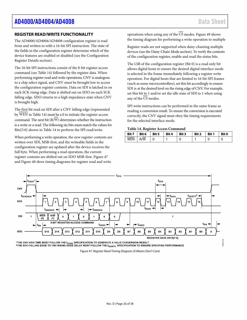
AD4000/AD4004/AD4008 Data Sheet
Rev. D | Page 26 of 38
REGISTER READ/WRITE FUNCTIONALITY The AD4000/AD4004/AD4008 configuration register is read from and written to with a 16-bit SPI instruction. The state of the fields in the configuration register determine which of the device features are enabled or disabled (see the Configuration Register Details section).
The 16-bit SPI instructions consist of the 8-bit register access command (see Table 14) followed by the register data. When performing register read and write operations, CNV is analogous to a chip select signal, and CNV must be brought low to access the configuration register contents. Data on SDI is latched in on each SCK rising edge. Data is shifted out on SDO on each SCK falling edge. SDO returns to a high impedance state when CNV is brought high.
The first bit read on SDI after a CNV falling edge (represented by WEN in Table 14) must be a 0 to initiate the register access command. The next bit (R/W) determines whether the instruction is a write or a read. The following six bits must match the values for Bits[5:0] shown in Table 14 to perform the SPI read/write.
When performing a write operation, the new register contents are written over SDI, MSB-first, and the writeable fields in the configuration register are updated after the device receives the full byte. When performing a read operation, the current register contents are shifted out on SDO MSB-first. Figure 47 and Figure 48 show timing diagrams for register read and write
operations when using any of the CS modes. Figure 49 shows the timing diagram for performing a write operation to multiple
Register reads are not supported when daisy-chaining multiple devices (see the Daisy-Chain Mode section). To verify the contents of the configuration register, enable and read the status bits.
The LSB of the configuration register (Bit 0) is a read only bit allows digital hosts to ensure the desired digital interface mode is selected in the frame immediately following a register write operation. For digital hosts that are limited to 16-bit SPI frames (such as some microcontrollers), set this bit accordingly to ensure SDI is at the desired level on the rising edge of CNV. For example, set this bit to 1 and/or set the idle state of SDI to 1 when using any of the CS modes.
SPI write instructions can be performed in the same frame as reading a conversion result. To ensure the conversion is executed correctly, the CNV signal must obey the timing requirements for the selected interface mode.
Table 14. Register Access Command Bit 7 Bit 6 Bit 5 Bit 4 Bit 3 Bit 2 Bit 1 Bit 0 WEN R/W 0 1 0 1 0 0
149
56-
018
tSCK
tSCKL
tSCKH
tSCNVSCK
tSSDISCK tHSDISCK
tCNVH1
tEN tHSDOtDSDOtDIS
tQUIET22
1 tCONV2 tQUIET2
XB0B1B2B3B4B5D15 D14 D13 D12 D11 D10 D9 D8 B7 B6
REGISTER DATA ON B[7:0]
SDO
0 1 0 1 0 01 1WEN(0)
R/W(1)
8-BIT REGISTER ACCESS COMMAND
SDI
1 2 3 4 5 6 7 8 9 10 11 12 13 14 15 16SCK
CNV
Figure 47. Register Read Timing Diagram (X Means Don’t Care)
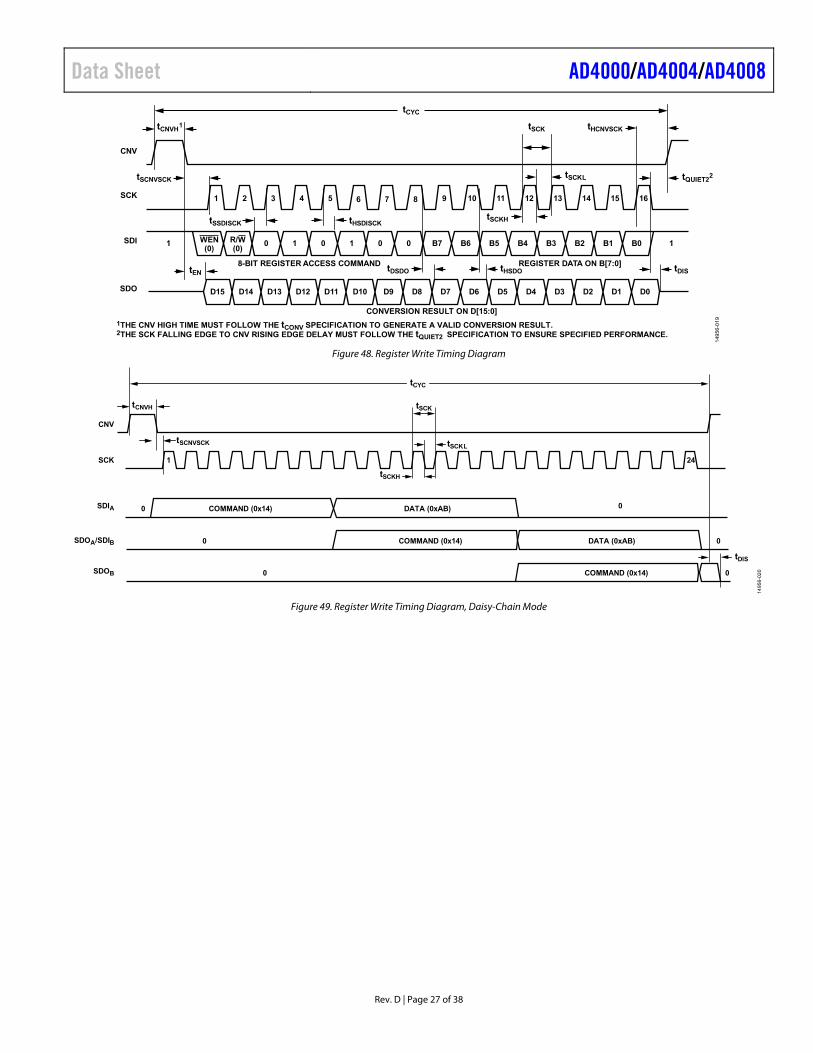
Data Sheet AD4000/AD4004/AD4008
Rev. D | Page 27 of 38
1495
6-01
9
tCYC
tSCK
tSCKL
tSCKH
tSCNVSCK
tSSDISCK tHSDISCK
tCNVH1
tEN tHSDOtDSDO tDIS
tHCNVSCK
tQUIET22
1THE CNV HIGH TIME MUST FOLLOW THE tCONV SPECIFICATION TO GENERATE A VALID CONVERSION RESULT.2THE SCK FALLING EDGE TO CNV RISING EDGE DELAY MUST FOLLOW THE tQUIET2 SPECIFICATION TO ENSURE SPECIFIED PERFORMANCE.
SDO D0D1D2D3D4D5D6D7D8D9D15 D14 D13 D12 D11 D10
CONVERSION RESULT ON D[15:0]
SDI 0 1 0 1R/WWEN B0B1B2B3B4B5B6B70 01 1(0) (0)
8-BIT REGISTER ACCESS COMMAND REGISTER DATA ON B[7:0]
SCK 1 2 3 4 5 6 7 8 9 10 11 12 13 14 15 16
CNV
Figure 48. Register Write Timing Diagram
SDIA
SDOA/SDIB
SDOB
0 0COMMAND (0x14)
0 0COMMAND (0x14)
0 0COMMAND (0x14)
tCYC
tSCK
tSCKL
tSCKH
tSCNVSCK
CNV
SCK 1 24
tDIS
tCNVH
DATA (0xAB)
DATA (0xAB)
1495
6-02
0
Figure 49. Register Write Timing Diagram, Daisy-Chain Mode
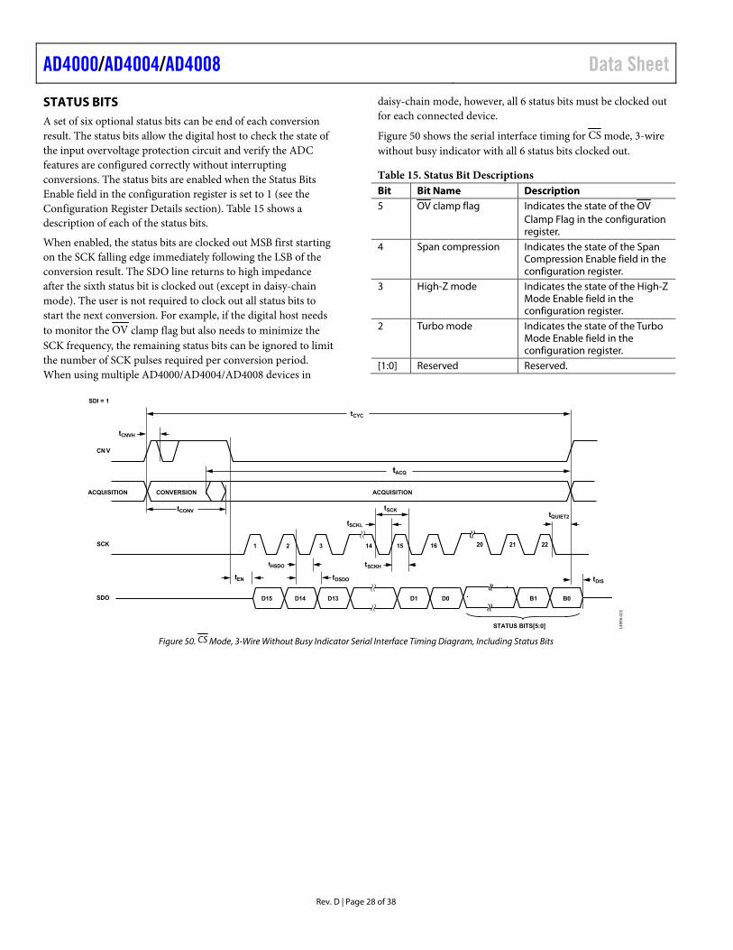
AD4000/AD4004/AD4008 Data Sheet
Rev. D | Page 28 of 38
STATUS BITS A set of six optional status bits can be end of each conversion result. The status bits allow the digital host to check the state of the input overvoltage protection circuit and verify the ADC features are configured correctly without interrupting conversions. The status bits are enabled when the Status Bits Enable field in the configuration register is set to 1 (see the Configuration Register Details section). Table 15 shows a description of each of the status bits.
When enabled, the status bits are clocked out MSB first starting on the SCK falling edge immediately following the LSB of the conversion result. The SDO line returns to high impedance after the sixth status bit is clocked out (except in daisy-chain mode). The user is not required to clock out all status bits to start the next conversion. For example, if the digital host needs to monitor the OV clamp flag but also needs to minimize the SCK frequency, the remaining status bits can be ignored to limit the number of SCK pulses required per conversion period. When using multiple AD4000/AD4004/AD4008 devices in
daisy-chain mode, however, all 6 status bits must be clocked out for each connected device.
Figure 50 shows the serial interface timing for CS mode, 3-wire without busy indicator with all 6 status bits clocked out.
Table 15. Status Bit Descriptions Bit Bit Name Description 5 OV clamp flag Indicates the state of the OV
Clamp Flag in the configuration register.
4 Span compression Indicates the state of the Span Compression Enable field in the configuration register.
3 High-Z mode Indicates the state of the High-Z Mode Enable field in the configuration register.
2 Turbo mode Indicates the state of the Turbo Mode Enable field in the configuration register.
[1:0] Reserved Reserved.
SDO D15 D14 D13 D1 D0
SCK 1 2 3 14 15 16
tSCK
tSCKL
tSCKHtHSDO
tDSDO
CN V
CONVERSIONACQUISITION
tCYC
ACQUISITION
SDI = 1
tCNVH
ACQ
tEN
21 22
tQUIET2
STATUS BITS[5:0]
B1
tDIS
B0
20
tCONV
149
56-
02
1
Figure 50. CS Mode, 3-Wire Without Busy Indicator Serial Interface Timing Diagram, Including Status Bits
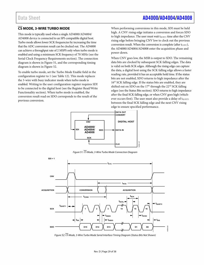
Data Sheet AD4000/AD4004/AD4008
Rev. D | Page 29 of 38
CS MODE, 3-WIRE TURBO MODE
This mode is typically used when a single AD4000/AD4004/ AD4008 device is connected to an SPI-compatible digital host. Turbo mode allows lower SCK frequencies by increasing the time that the ADC conversion result can be clocked out. The AD4000 can achieve a throughput rate of 2 MSPS only when turbo mode is enabled and using a minimum SCK frequency of 70 MHz (see the Serial Clock Frequency Requirements section). The connection diagram is shown in Figure 51, and the corresponding timing diagram is shown in Figure 52.
To enable turbo mode, set the Turbo Mode Enable field in the configuration register to 1 (see Table 12). This mode replaces the 3-wire with busy indicator mode when turbo mode is enabled. Writing to the user configuration register requires SDI to be connected to the digital host (see the Register Read/Write Functionality section). When turbo mode is enabled, the conversion result read on SDO corresponds to the result of the previous conversion.
When performing conversions in this mode, SDI must be held high. A CNV rising edge initiates a conversion and forces SDO to high impedance. The user must wait tQUIET1 time after the CNV rising edge before bringing CNV low to clock out the previous conversion result. When the conversion is complete (after tCONV), the AD4000/AD4004/AD4008 enter the acquisition phase and power-down.
When CNV goes low, the MSB is output to SDO. The remaining data bits are clocked by subsequent SCK falling edges. The data is valid on both SCK edges. Although the rising edge can capture the data, a digital host using the SCK falling edge allows a faster reading rate, provided it has an acceptable hold time. If the status bits are not enabled, SDO returns to high impedance after the 16th SCK falling edge. If the status bits are enabled, they are shifted out on SDO on the 17th through the 22nd SCK falling edges (see the Status Bits section). SDO returns to high impedance after the final SCK falling edge, or when CNV goes high (which-ever occurs first). The user must also provide a delay of tQUIET2 between the final SCK falling edge and the next CNV rising edge to ensure specified performance.
AD4000/AD4004/AD4008
SDI SDO
CNV
SCK
CONVERTDATA OUT
DATA IN
CLK
DIGITAL HOST
1495
6-14
7
Figure 51. CS Mode, 3-Wire Turbo Mode Connection Diagram
SDI = 1
tCYC
CNV
ACQUISITION ACQUISITION
tACQ
tSCK
tSCKL
CONVERSION
SCK
D0D1D13D14D15SDO
tEN
tHSDO
1 2 3 14 15 16
tDSDO tDIS
tSCKH
tQUIET1QUIET2
CONV
1495
6-02
6
Figure 52. CS Mode, 3-Wire Turbo Mode Serial Interface Timing Diagram (Status Bits Not Shown)
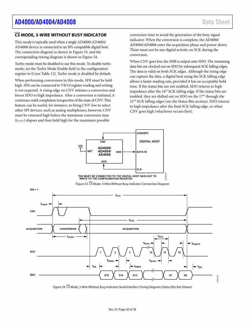
AD4000/AD4004/AD4008 Data Sheet
Rev. D | Page 30 of 38
CS MODE, 3-WIRE WITHOUT BUSY INDICATOR
This mode is typically used when a single AD4000/AD4004/ AD4008 device is connected to an SPI-compatible digital host. The connection diagram is shown in Figure 53, and the corresponding timing diagram is shown in Figure 54.
Turbo mode must be disabled to use this mode. To disable turbo mode, set the Turbo Mode Enable field in the configuration register to 0 (see Table 12). Turbo mode is disabled by default.
When performing conversions in this mode, SDI must be held high. SDI can be connected to VIO if register reading and writing is not required. A rising edge on CNV initiates a conversion and forces SDO to high impedance. After a conversion is initiated, it continues until completion irrespective of the state of CNV. This feature can be useful, for instance, to bring CNV low to select other SPI devices, such as analog multiplexers; however, CNV must be returned high before the minimum conversion time (tCONV) elapses and then held high for the maximum possible
conversion time to avoid the generation of the busy signal indicator. When the conversion is complete, the AD4000/ AD4004/AD4008 enter the acquisition phase and power-down. There must not be any digital activity on SCK during the conversion.
When CNV goes low, the MSB is output onto SDO. The remaining data bits are clocked out on SDO by subsequent SCK falling edges. The data is valid on both SCK edges. Although the rising edge can capture the data, a digital host using the SCK falling edge allows a faster reading rate, provided it has an acceptable hold time. If the status bits are not enabled, SDO returns to high impedance after the 16th SCK falling edge. If the status bits are enabled, they are shifted out on SDO on the 17th through the 22nd SCK falling edges (see the Status Bits section). SDO returns to high impedance after the final SCK falling edge, or when CNV goes high (whichever occurs first).
AD4000/AD4004/AD4008
SDI1 SDO
CNV
SCK
CONVERT
DATA IN
CLK
DIGITAL HOST
VIO
149
56-0
22
1SDI MUST BE CONNECTED TO THE DIGITAL HOST DATA OUT TO WRITE TO THE CONFIGURATION REGISTER.
Figure 53. CS Mode, 3-Wire Without Busy Indicator Connection Diagram
SDO D15 D14 D13 D1 D0
tDIS
SCK 1 2 3 14 15 16
tSCK
tSCKL
tSCKHtHSDO
tDSDO
CNV
CONVERSIONACQUISITION
tCYC
ACQUISITION
SDI = 1
tCNVH
tACQ
tEN
tQUIET2
tCONV
1495
6-02
3
Figure 54. CS Mode, 3-Wire Without Busy Indicator Serial Interface Timing Diagram (Status Bits Not Shown)

Data Sheet AD4000/AD4004/AD4008
Rev. D | Page 31 of 38
CS MODE, 3-WIRE WITH BUSY INDICATOR
This mode is typically used when a single AD4000/AD4004/ AD4008 device is connected to an SPI-compatible digital host with an interrupt input (IRQ). The connection diagram is shown in Figure 55, and the corresponding timing diagram is shown in Figure 56.
Turbo mode must be disabled to use this mode. To disable turbo mode, set the Turbo Mode Enable field in the configuration register to 0 (see Table 12). Turbo mode is disabled by default.
When performing conversions in this mode, SDI must be held high. SDI can be connected to VIO if register reading and writing is not required. A rising edge on CNV initiates a conversion and forces SDO to high impedance. SDO remains high impedance until the completion of the conversion, irrespective of the state of CNV. Prior to the minimum conversion time, CNV can select other SPI devices, such as analog multiplexers; however, CNV must be returned low before the minimum conversion time (tCONV) elapses and then held low for the maximum possible conversion time to guarantee the generation of the busy signal indicator. When the conversion is complete, the AD4000/AD4004/AD4008
then enter the acquisition phase and power-down. There must not be any digital activity on the SCK during the conversion.
When the conversion is complete, SDO is driven low. With a pull-up resistor (for example, 1 kΩ) on the SDO line, this transition can be used as an interrupt signal to initiate the data reading controlled by the digital host. The data bits are then clocked out MSB first on SDO by subsequent SCK falling edges. The data is valid on both SCK edges. Although the rising edge can capture the data, a digital host using the SCK falling edge allows a faster reading rate, provided it has an acceptable hold time. The conver-sion result is clocked out on SDO on the first 16 SCK falling edges. If the status bits are enabled, they are clocked out on SDO on the 17th through the 22nd SCK falling edges (see the Status Bits section). SDO returns to high impedance after an optional additional SCK falling edge or the next CNV rising edge (whichever occurs first).
If multiple AD4000/AD4004/AD4008 devices are selected at the same time, the SDO output pin handles this contention without damage or induced latch-up. It is recommended to keep this contention as short as possible to limit extra power dissipation.
SDI SDO
CNV
SCK
CONVERT
DATA IN
CLK
DIGITAL HOST
VIO
IRQ
VIO
1kΩ
AD4000/AD4004/AD4008
149
56-0
24
1SDI MUST BE CONNECTED TO THE DIGITAL HOST DATA OUT TO WRITE TO THE CONFIGURATION REGISTER. Figure 55. CS Mode, 3-Wire with Busy Indicator Connection Diagram
SDO D15 D14 D1 D0
tDIS
SCK 1 2 3 15 16 17
tSCK
tSCKL
tSCKHtHSDO
tDSDO
CNV
CONVERSIONACQUISITION
tCONV
tCYC
ACQUISITION
SDI = 1
tCNVH
tACQ
tQUIET2
149
56
-02
5
Figure 56. CS Mode, 3-Wire with Busy Indicator Serial Interface Timing Diagram (Status Bits Not Shown)
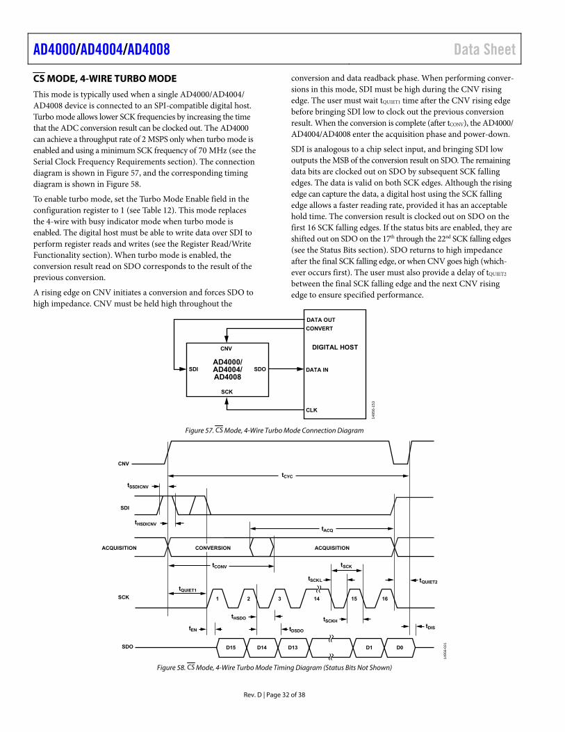
AD4000/AD4004/AD4008 Data Sheet
Rev. D | Page 32 of 38
CS MODE, 4-WIRE TURBO MODE
This mode is typically used when a single AD4000/AD4004/ AD4008 device is connected to an SPI-compatible digital host. Turbo mode allows lower SCK frequencies by increasing the time that the ADC conversion result can be clocked out. The AD4000 can achieve a throughput rate of 2 MSPS only when turbo mode is enabled and using a minimum SCK frequency of 70 MHz (see the Serial Clock Frequency Requirements section). The connection diagram is shown in Figure 57, and the corresponding timing diagram is shown in Figure 58.
To enable turbo mode, set the Turbo Mode Enable field in the configuration register to 1 (see Table 12). This mode replaces the 4-wire with busy indicator mode when turbo mode is enabled. The digital host must be able to write data over SDI to perform register reads and writes (see the Register Read/Write Functionality section). When turbo mode is enabled, the conversion result read on SDO corresponds to the result of the previous conversion.
A rising edge on CNV initiates a conversion and forces SDO to high impedance. CNV must be held high throughout the
conversion and data readback phase. When performing conver-sions in this mode, SDI must be high during the CNV rising edge. The user must wait tQUIET1 time after the CNV rising edge before bringing SDI low to clock out the previous conversion result. When the conversion is complete (after tCONV), the AD4000/ AD4004/AD4008 enter the acquisition phase and power-down.
SDI is analogous to a chip select input, and bringing SDI low outputs the MSB of the conversion result on SDO. The remaining data bits are clocked out on SDO by subsequent SCK falling edges. The data is valid on both SCK edges. Although the rising edge can capture the data, a digital host using the SCK falling edge allows a faster reading rate, provided it has an acceptable hold time. The conversion result is clocked out on SDO on the first 16 SCK falling edges. If the status bits are enabled, they are shifted out on SDO on the 17th through the 22nd SCK falling edges (see the Status Bits section). SDO returns to high impedance after the final SCK falling edge, or when CNV goes high (which-ever occurs first). The user must also provide a delay of tQUIET2 between the final SCK falling edge and the next CNV rising edge to ensure specified performance.
AD4000/AD4004/AD4008
SDI SDO
CNV
SCK
CONVERT
DATA IN
CLK
DIGITAL HOST
DATA OUT
14
95
6-1
53
Figure 57. CS Mode, 4-Wire Turbo Mode Connection Diagram
ACQUISITION
SDO
SCK
ACQUISITION
SDI
CNV
tSSDICNV
tHSDICNV
tCYC
tSCK
tSCKL
tEN
tHSDO
1 2 3 14 15 16
tDSDOtDIS
tSCKH
D15 D14 D13 D1 D0
tQUIET1
tQUIET2
tACQ
CONVERSION
tCONV
149
56-0
31
Figure 58. CS Mode, 4-Wire Turbo Mode Timing Diagram (Status Bits Not Shown)

Data Sheet AD4000/AD4004/AD4008
Rev. D | Page 33 of 38
CS MODE, 4-WIRE WITHOUT BUSY INDICATOR
This mode is typically used when multiple AD4000/AD4004/ AD4008 devices are connected to an SPI-compatible digital host. A connection diagram example using two AD4000/AD4004/ AD4008 devices is shown in Figure 59, and the corresponding timing diagram is shown in Figure 60.
Turbo mode must be disabled to use this mode. To disable turbo mode, set the Turbo Mode Enable field in the configuration register to 0 (see Table 12). Turbo mode is disabled by default.
A rising edge on CNV initiates a conversion and forces SDO to high impedance. When performing conversions in this mode, SDI must be high during the CNV rising edge. CNV must be held high throughout the conversion and data readback phase. When performing conversions in this mode, SDI must be high during the CNV rising edge. Prior to the minimum conversion time (tCONV), SDI can select other SPI devices, such as analog multiplexers; however, SDI must be returned high before the minimum conversion time elapses and then held high for the
maximum possible conversion time to avoid the generation of the busy signal indicator. When the conversion is complete, the AD4000/AD4004/AD4008 enter the acquisition phase and power-down. There must not be any digital activity on SCK during the conversion.
SDI is analogous to a chip select input, and each ADC result can be read by bringing its SDI input low. Bringing SDI low on each device outputs the MSB of the conversion result on its SDO pin. The remaining data bits are clocked out on SDO by subsequent SCK falling edges. The data is valid on both SCK edges. The conversion result is clocked out on SDO on the first 16 SCK falling edges. If the status bits are enabled, they are shifted out on SDO on the 17th through the 22nd SCK falling edges (see the Status Bits section). SDO returns to high impedance after the final SCK falling edge, or when SDI goes high (whichever occurs first). If the SDO of each device is tied together, ensure SDI is only low for one device at a time. The user must also provide a delay of tQUIET2 between the final SCK falling edge and the next CNV rising edge to ensure specified performance.
AD4000/AD4004/AD4008
SDI SDO
CNV
SCK
DEVICE A
CONVERT
DATA INCLK
DIGITAL HOSTAD4000/AD4004/AD4008
SDI SDO
CNV
SCK
DEVICE B
1495
6-02
7
CS1CS2
Figure 59. CS Mode, 4-Wire Without Busy Indicator Connection Diagram
SDO D15 D14 D13 D1 D0
tDIS
SCK 1 2 3 30 31 32
tHSDO
tDSDOtEN
CONVERSIONACQUISITION
tCONV
tCYC
tACQ
ACQUISITION
SDI(CS1)
CNV
tSSDICNV
tHSDICNV
D1
14 15
tSCK
tSCKL
tSCKH
D0 D15 D14
17 1816
SDI(CS2)
tQUIET2
1495
6-02
8
Figure 60. CS Mode, 4-Wire Without Busy Indicator Serial Interface Timing Diagram (Status Bits Not Shown)
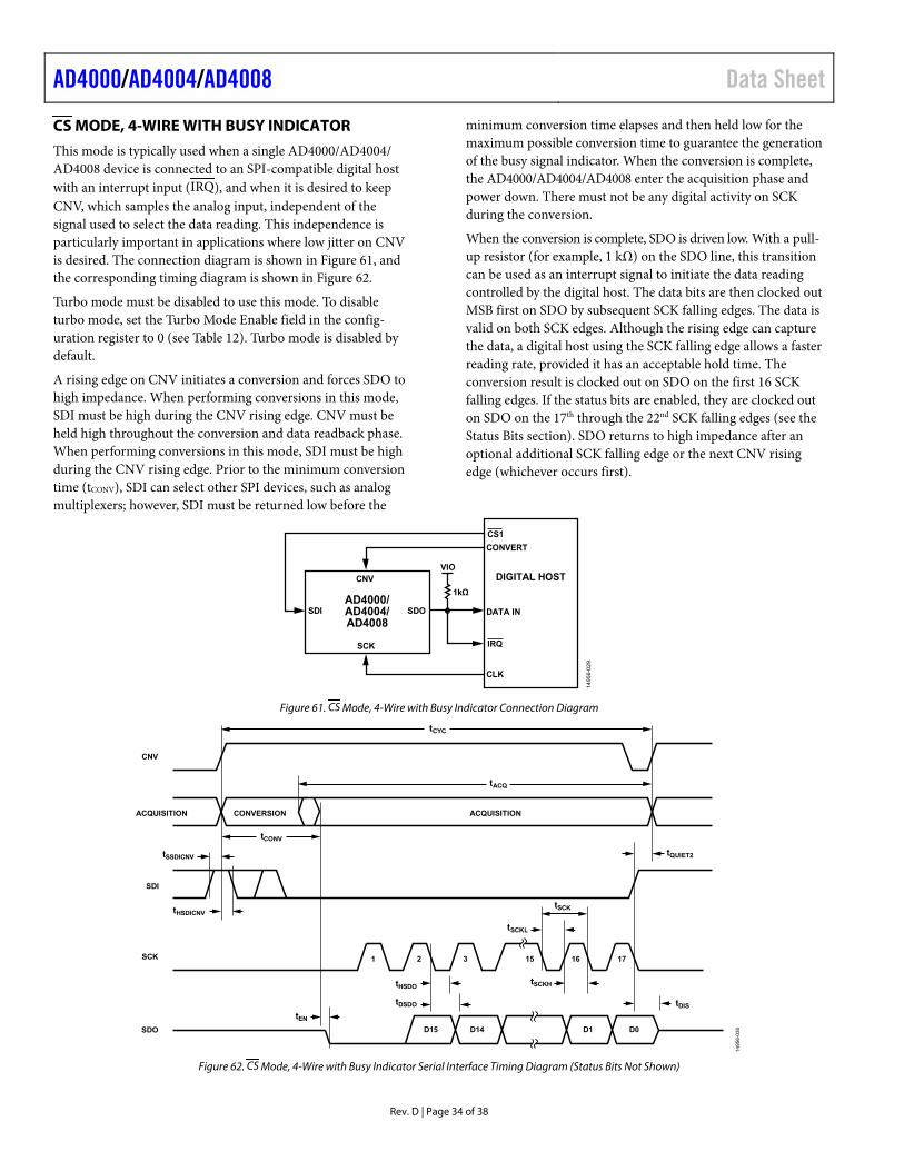
AD4000/AD4004/AD4008 Data Sheet
Rev. D | Page 34 of 38
CS MODE, 4-WIRE WITH BUSY INDICATOR
This mode is typically used when a single AD4000/AD4004/ AD4008 device is connected to an SPI-compatible digital host with an interrupt input (IRQ), and when it is desired to keep CNV, which samples the analog input, independent of the signal used to select the data reading. This independence is particularly important in applications where low jitter on CNV is desired. The connection diagram is shown in Figure 61, and the corresponding timing diagram is shown in Figure 62.
Turbo mode must be disabled to use this mode. To disable turbo mode, set the Turbo Mode Enable field in the config-uration register to 0 (see Table 12). Turbo mode is disabled by default.
A rising edge on CNV initiates a conversion and forces SDO to high impedance. When performing conversions in this mode, SDI must be high during the CNV rising edge. CNV must be held high throughout the conversion and data readback phase. When performing conversions in this mode, SDI must be high during the CNV rising edge. Prior to the minimum conversion time (tCONV), SDI can select other SPI devices, such as analog multiplexers; however, SDI must be returned low before the
minimum conversion time elapses and then held low for the maximum possible conversion time to guarantee the generation of the busy signal indicator. When the conversion is complete, the AD4000/AD4004/AD4008 enter the acquisition phase and power down. There must not be any digital activity on SCK during the conversion.
When the conversion is complete, SDO is driven low. With a pull-up resistor (for example, 1 kΩ) on the SDO line, this transition can be used as an interrupt signal to initiate the data reading controlled by the digital host. The data bits are then clocked out MSB first on SDO by subsequent SCK falling edges. The data is valid on both SCK edges. Although the rising edge can capture the data, a digital host using the SCK falling edge allows a faster reading rate, provided it has an acceptable hold time. The conversion result is clocked out on SDO on the first 16 SCK falling edges. If the status bits are enabled, they are clocked out on SDO on the 17th through the 22nd SCK falling edges (see the Status Bits section). SDO returns to high impedance after an optional additional SCK falling edge or the next CNV rising edge (whichever occurs first).
AD4000/AD4004/AD4008
SDI SDO
CNV
SCK
CONVERT
DATA IN
CLK
DIGITAL HOST
IRQ
VIO
1kΩ
CS1
1495
6-02
9
Figure 61. CS Mode, 4-Wire with Busy Indicator Connection Diagram
SDO D15 D14 D1 D0
tDIS
SCK 1 2 3 15 16 17
tSCK
tSCKL
tSCKHtHSDO
tDSDO
tEN
CONVERSIONACQUISITION
tCONV
tCYC
tACQ
ACQUISITION
SDI
CNV
tSSDICNV
tHSDICNV
tQUIET2
1495
6-03
0
Figure 62. CS Mode, 4-Wire with Busy Indicator Serial Interface Timing Diagram (Status Bits Not Shown)
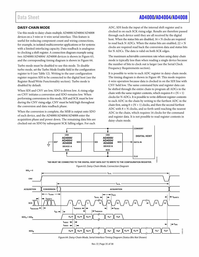
Data Sheet AD4000/AD4004/AD4008
Rev. D | Page 35 of 38
DAISY-CHAIN MODE Use this mode to daisy-chain multiple AD4000/AD4004/AD4008 devices on a 3-wire or 4-wire serial interface. This feature is useful for reducing component count and wiring connections, for example, in isolated multiconverter applications or for systems with a limited interfacing capacity. Data readback is analogous to clocking a shift register. A connection diagram example using two AD4000/AD4004/ AD4008 devices is shown in Figure 63, and the corresponding timing diagram is shown in Figure 64.
Turbo mode must be disabled to use this mode. To disable turbo mode, set the Turbo Mode Enable field in the configuration register to 0 (see Table 12). Writing to the user configuration register requires SDI to be connected to the digital host (see the Register Read/Write Functionality section). Turbo mode is disabled by default.
When SDI and CNV are low, SDO is driven low. A rising edge on CNV initiates a conversion and SDO remains low. When performing conversions in this mode, SDI and SCK must be low during the CNV rising edge. CNV must be held high throughout the conversion and data readback phase.
When the conversion is complete, the MSB is output onto SDO of each device, and the AD4000/AD4004/AD4008 enter the acquisition phase and power down. The remaining data bits are clocked out on SDO by subsequent SCK falling edges. For each
ADC, SDI feeds the input of the internal shift register and is clocked in on each SCK rising edge. Results are therefore passed through each device until they are all received by the digital host. When the status bits are disabled, 16 × N clocks are required to read back N ADCs. When the status bits are enabled, 22 × N clocks are required read back the conversion data and status bits for N ADCs. The data is valid on both SCK edges.
The maximum achievable conversion rate when using daisy-chain mode is typically less than when reading a single device because the number of bits to clock out is larger (see the Serial Clock Frequency Requirements section).
It is possible to write to each ADC register in daisy-chain mode. The timing diagram is shown in Figure 49. This mode requires 4-wire operation because data is clocked in on the SDI line with CNV held low. The same command byte and register data can be shifted through the entire chain to program all ADCs in the chain with the same register contents, which requires 8 × (N + 1) clocks for N ADCs. It is possible to write different register contents to each ADC in the chain by writing to the furthest ADC in the chain first, using 8 × (N + 1) clocks, and then the second furthest ADC with 8 × N clocks, and so forth until reaching the nearest ADC in the chain, which requires 16 clocks for the command and register data. It is not possible to read register contents in daisy-chain mode.
CONVERT
DATA IN
CLK
DIGITAL HOST
DEVICE BDEVICE A
AD4000/AD4004/AD4008SDI1
1SDI MUST BE CONNECTED TO THE DIGITAL HOST DATA OUT TO WRITE TO THE CONFIGURATION REGISTER.
SDO
CNV
SCK
AD4000/AD4004/AD4008SDI SDO
CNV
SCK
1495
6-03
2
Figure 63. Daisy-Chain Mode, Connection Diagram
SDOA = SDIB DA15
DB15 DB14 DB13
DA14 DA13 DA1 DA0
DA1 DA0DB1 DB0
SCK 1 2 3 30 31 32
tSSDISCKtHSDISCK
CONVERSIONACQUISITION
tCONV
tCYC
tACQ
ACQUISITION
CNV
14 15
tSCKtSCKL
tSCKH
17 1816
SDIA = 0
SDOB DA15 DA14
tHSDO
tDSDO
tQUIET2
tHSCKCNV
tDIS
tQUIET2
tEN
1495
6-03
3
Figure 64. Daisy-Chain Mode, Serial Interface Timing Diagram (Status Bits Not Shown)

AD4000/AD4004/AD4008 Data Sheet
Rev. D | Page 36 of 38
LAYOUT GUIDELINES The PCB that houses the AD4000/AD4004/AD4008 must be designed so that the analog and digital sections are separated and confined to certain areas of the board. The pinout of the AD4000/AD4004/AD4008, with its analog signals on the left side and its digital signals on the right side, eases this task.
Avoid running digital lines under the device because they couple noise onto the die, unless a ground plane under the AD4000/ AD4004/AD4008 is used as a shield. Fast switching signals, such as CNV or clocks, must not run near analog signal paths. Avoid crossover of digital and analog signals.
At least one ground plane must be used. It can be common or split between the digital and analog sections. In the latter case, join the planes underneath the AD4000/AD4004/AD4008 devices.
The AD4000/AD4004/AD4008 voltage reference input (REF) has a dynamic input impedance. Decouple the REF pin with minimal parasitic inductances by placing the reference decoupling ceramic capacitor close to (ideally right up against) the REF and GND pins and connect them with wide, low impedance traces.
Finally, decouple the VDD and VIO power supplies of the AD4000/AD4004/AD4008 with ceramic capacitors, typically 0.1 μF, placed close to the AD4000/AD4004/AD4008 and connected using short, wide traces to provide low impedance paths and to reduce the effect of glitches on the power supply lines.
An example of the AD4000 layout following these rules is shown in Figure 65 and Figure 66. Note that the AD4004/ AD4008 layout is equivalent to the AD4000 layout.
EVALUATING THE AD4000/AD4004/AD4008 PERFORMANCE Other recommended layouts for the AD4000/AD4004/AD4008 are outlined in the user guide of the evaluation board for the AD4000 (EVAL-AD4000FMCZ). The evaluation board package includes a fully assembled and tested evaluation board with the AD4000, documentation, and software for controlling the board from a PC via the EVAL-SDP-CH1Z. The EVAL-AD4000FMCZ can also be used to evaluate the AD4004/AD4008 by limiting the throughput to 1 MSPS/500 kSPS, respectively, in its software (see the UG-1042).
1495
6-0
34
Figure 65. Example Layout of the AD4000 (Top Layer)
14
95
6-0
35
Figure 66. Example Layout of the AD4000 (Bottom Layer)

Data Sheet AD4000/AD4004/AD4008
Rev. D | Page 37 of 38
OUTLINE DIMENSIONS
COMPLIANT TO JEDEC STANDARDS MO-187-BA 091
70
9-A
6°0°
0.700.550.40
5
10
1
6
0.50 BSC
0.300.15
1.10 MAX
3.103.002.90
COPLANARITY0.10
0.230.13
3.103.002.90
5.154.904.65
PIN 1IDENTIFIER
15° MAX0.950.850.75
0.150.05
Figure 67. 10-Lead Mini Small Outline Package [MSOP]
(RM-10) Dimensions shown in millimeters
2.482.382.23
0.500.400.30
10
1
6
5
0.300.250.20
0.800.750.70
1.741.641.49
0.20 REF
0.05 MAX0.02 NOM
0.50 BSC
EXPOSEDPAD
3.103.00 SQ2.90
COPLANARITY0.08
TOP VIEW
SIDE VIEW
BOTTOM VIEW
0.20 MIN
PK
G-0
0436
2
08-2
0-20
18-C
FOR PROPER CONNECTION OFTHE EXPOSED PAD, REFER TOTHE PIN CONFIGURATION ANDFUNCTION DESCRIPTIONSSECTION OF THIS DATA SHEET.
PIN 1IN D IC ATO R AR E A OP TIO N S(SEE DETAIL A)
DETAIL A(JEDEC 95)
PIN 1INDICATOR
AREA
SEATINGPLANE
Figure 68. 10-Lead Lead Frame Chip Scale Package [LFCSP]
3 mm × 3 mm Body and 0.75 mm Package Height (CP-10-9)
Dimensions shown in millimeters
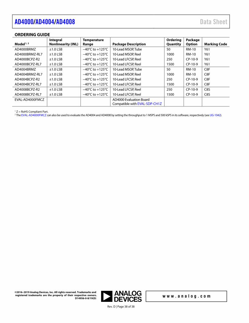
AD4000/AD4004/AD4008 Data Sheet
Rev. D | Page 38 of 38
ORDERING GUIDE
Model1, 2 Integral Nonlinearity (INL)
Temperature Range Package Description
Ordering Quantity
Package Option Marking Code
AD4000BRMZ ±1.0 LSB −40°C to +125°C 10-Lead MSOP, Tube 50 RM-10 Y61 AD4000BRMZ-RL7 ±1.0 LSB −40°C to +125°C 10-Lead MSOP, Reel 1000 RM-10 Y61 AD4000BCPZ-R2 ±1.0 LSB −40°C to +125°C 10-Lead LFCSP, Reel 250 CP-10-9 Y61 AD4000BCPZ-RL7 ±1.0 LSB −40°C to +125°C 10-Lead LFCSP, Reel 1500 CP-10-9 Y61 AD4004BRMZ ±1.0 LSB −40°C to +125°C 10-Lead MSOP, Tube 50 RM-10 C8F AD4004BRMZ-RL7 ±1.0 LSB −40°C to +125°C 10-Lead MSOP, Reel 1000 RM-10 C8F AD4004BCPZ-R2 ±1.0 LSB −40°C to +125°C 10-Lead LFCSP, Reel 250 CP-10-9 C8F AD4004BCPZ-RL7 ±1.0 LSB −40°C to +125°C 10-Lead LFCSP, Reel 1500 CP-10-9 C8F AD4008BCPZ-R2 ±1.0 LSB −40°C to +125°C 10-Lead LFCSP, Reel 250 CP-10-9 C8S AD4008BCPZ-RL7 ±1.0 LSB −40°C to +125°C 10-Lead LFCSP, Reel 1500 CP-10-9 C8S EVAL-AD4000FMCZ AD4000 Evaluation Board
Compatible with EVAL-SDP-CH1Z
1 Z = RoHS Compliant Part. 2 The EVAL-AD4000FMCZ can also be used to evaluate the AD4004 and AD4008 by setting the throughput to 1 MSPS and 500 kSPS in its software, respectively (see UG-1042).
©2016–2019 Analog Devices, Inc. All rights reserved. Trademarks and registered trademarks are the property of their respective owners. D14956-0-8/19(D)