9 chip bonding at the first level - the chip collection
TRANSCRIPT

The I/O interface to the die primarily interconnects electrical power, ground and signals. It must
provide for low impedance for the power distribution system, so as to keep switching noise within
specification, and controlled impedance for the signal leads to allow adequate signal integrity. In
addition it must accommodate all the I/O and power and ground leads required, and at the same
time, minimize the cost for high volume assembly.
The secondary role of chip bonding is to be mechanically robust, not interfere with thermal man-
agement and be the geometrical transformer from the die features to the next level of packaging
features. There are many options for the next level of interconnect, including:
¥ leadframe in a single chip package
¥ ceramic substrate in a single chip package
¥ laminate substrate in a single chip package
¥ ceramic substrate in a multichip module
¥ laminate substrate in a multichip module
¥ glass substrate, such as an LCD (liquid crystal display)
¥ laminate substrate, such as a circuit board
¥ ceramic substrate, such as a circuit board
For all of these first level interfaces, the chip bonding options are the same. Illustrated in Figure
9-1, they are:
¥ wirebond
¥ TAB (tape automated bonding)
¥ flip chip; either with a solder interface, a polymer adhesive or a welded joint
Because of the parallel efforts in widely separated applications involving similar, but slightly dif-
ferent variations of chip attach techniques, seemingly confusing names have historically evolved
to describe some of the attach technologies.
COG (chip on glass) refers to assembly of bare die onto LCD panels. This can typically be flip
chip, ACF (anisotropic conductive film) attach, or less commonly, wirebonding to gold or alu-
minum pads metallized on the glass. TAB attach to glass is sometimes referred to as COG as well.
INTEGRATED CIRCUIT ENGINEERING CORPORATION 9-1
9 CHIP BONDING AT THE FIRST LEVEL

COB (chip on board) refers to assembly of bare die onto a laminate substrate, such as FR-4, with
wirebonding. This is sometimes referred to as MCM-L.
DCA (direct chip attach) refers to flip chip attach of a bare die to a laminate substrate. It is distin-
guished from COB by the use of flip chip bonding rather than wirebonding. DCA is also a form
of MCM-L. Flip chip, when used with ceramic MCMs, is usually referred to as FC-MCM.
TCP (tape carrier package) refers to a chip already attached to a TAB leadframe. The use of the
term TCP has become a popular replacement for the term TAB because TAB has recently suffered
in image from not having lived up to its promises in the U.S.
Chip Bonding at the First Level
INTEGRATED CIRCUIT ENGINEERING CORPORATION9-2
Courtesy of IBM
Source: ICE, “Roadmaps of Packaging Technology” 22212
Source: IEPS 1990
Source: Motorola
WirebondClose up
TAB
Flip Chip
Figure 9-1. The Three Principle Methods for Chip Bonding at the First Level

Electrical Issues
The most important electrical properties of the first level bond to the chip is the lead inductance
and resistance. The leading order term that influences the lead inductance is the length of the lead.
The shorter the interconnect, the lower the inductance. As pointed out in a previous chapter,
lower inductance in the power and ground path will decrease ground bounce and switching noise.
To first order, the lead inductance of a wirebond is about 1nH/mm, or 25nH/inch. A wirebond
50mils long will have a lead inductance of 1.3nH. A solder ball used in C4, 5mils tall, will have
an inductance on the order of 0.13nH. At this scale, other factors than the length of the intercon-
nect dominate the inductance, but it will still be significantly below that of a wirebond. A TAB
lead, 200mils long, might have a lead inductance of 5nH.
The second important term is resistance. This will affect the DC voltage drop in power and
ground paths. A wirebond, 1mil in diameter has a resistance of about 1 Ohm/inch. For a wire
50mils long, the resistance is about 50mOhms. With the typically 0.25A limit for a single wire-
bond, the DC voltage drop might be 12mV, below the typical noise budget for even a 3V system.
Shorter lengths and wider cross sections contribute to lower resistance.
The typical electrical properties of the various interconnects are summarized in Figure 9-2.
WIREBONDING
Over 93 percent of all chips are electrically connected by wirebonding. In 1996, this corresponded
to over 1 trillion wirebonds. Assuming 100mils as the average bond, this is 100 billion inches, or
2.5 million kilometers of wire, enough wire to make four round trips from the earth to the moon.
Yet, with the universal use of wirebonding, and its high volume, it is also the most common source
of failure for an IC. 26% of all IC failures are related to the wirebond. Figure 9-3 shows the fail-
ure mechanism breakdown for packaged die.
Chip Bonding at the First Level
INTEGRATED CIRCUIT ENGINEERING CORPORATION 9-3
22510Source: ICE, "Roadmaps of Packaging Technology"
Wirebond
TAB
Flip Chip
1 Ohm/inch
0.25 Ohm/inch
0.08 Ohm/inch
25nH/inch
21nH/inch
18nH/inch
50-100mils
100-300mils
3-6mils
50-100mOhms
25-75mOhms
<1mOhm
1.2-2.5nH
2.1-6.3nH
<0.1nH
ResistancePer Length
TypicalLengths
TypicalResistances
TypicalInductances
InductancePer Length
Figure 9-2. Summary of Electrical Properties of Chip Bonding Technologies

The reason wirebonding is so popular is:
¥ it works
¥ virtually all die are compatible with it
¥ it is robust
¥ it is very mature- all of the known problems have known solutions
¥ the yield can be very high, typically 100ppm defects per wirebond
¥ alternatives are riskier
¥ there is a well established infrastructure to support it
¥ the capital expense for a small shop to get started in wirebonding is less than $20k
¥ it is flexible- no tooling charges for different chips and packages
¥ it can accommodate die shrinks without requiring a package change
Any alternative processes that may catch on must have a very compelling motivation.
Gold Versus Aluminum Wirebonding
Two types of wires are typically used, gold and aluminum. Each has a different assembly process,
equipment and operating conditions.
The process for aluminum wirebonding is illustrated in Figure 9-4. The fine wire is threaded
through a micro machined capillary tube that precision aligns the end of the wire over the die pad
and forms the ultrasonic weld. A close up of the wedge tool is shown in Figure 9-5. A magnified
view of the bond on the chip is shown in Figure 9-6.
Chip Bonding at the First Level
INTEGRATED CIRCUIT ENGINEERING CORPORATION9-4
Source: Solid State Technology/ICE, "Roadmaps of Packaging Technology"
22511
*Four-year average
Wirebonds26%
Test Errors19%
Contamination15%
Metallization9%
Diffusion/Oxidation
13%
Die Attach6%
Package5%
Other4%
Cracked Die2%
Figure 9-3. Vendor Related Failures: Screened Parts

After the first bond is made, and the aluminum wire is welded to the aluminum pad, the tool
moves the wire through space to form a loop, ending on the next level pad, usually on the bond-
ing shelf of a package. The tool next comes down and ultrasonically welds the aluminum wire to
the second pad. The heel of the tool severely weakens the tail of the weld on the pad. The tool
then clamps hold of the wire and pulls up, breaking the wire at the heel. The tool is then ready to
repeat the process on the next chip pad.
The metallization on the chip is typically aluminum and the metallization on the second pad is
typically gold or silver plated copper. The bonding is performed at room temperature and the
weld is accomplished with pressure and ultrasonic energy, hence the name, ultrasonic bonding.
The process for gold wirebonding is illustrated in Figure 9-7. The end of the gold wire is melted
in a micro spark at the tip of a capillary tube. A close up of the capillary tube for gold ball bond-
ing is shown in Figure 9-8. The ball is aligned over the pad on the die and the combination of heat,
pressure and ultrasonic energy welds the gold ball to the aluminum die pad.
Chip Bonding at the First Level
INTEGRATED CIRCUIT ENGINEERING CORPORATION 9-5
���������������������������
Wedgetool
Die������������������������
Al Wire
������������������������
Pressure and ultrasonicenergy to form
Bond
231
����������������
4
����������������
Post of Leadframe
���������������� ��������
��������
5
Post����������������
6
Post
Pressure and ultrasonicenergy to bond
15027BSource: National Bureau of Standards/ICE, “Roadmaps on Packaging Solutions”
Al Bonding
Pad
Die Die
Die
Die
Figure 9-4. Ultrasonic Bonding Sequence

Chip Bonding at the First Level
INTEGRATED CIRCUIT ENGINEERING CORPORATION9-6
Source: Micro Swiss/ 22512ICE, “Roadmaps of Packaging Technology”
Figure 9-5. Close Up of Aluminum Wire Bonding Tool
Figure 9-6. Aluminum Wedge Bond on an IC
Source: ICE, “Roadmaps of Packaging Technology” 22537

When just heat and pressure is used, the process is termed thermocompression bonding. In order
to form a reliable gold-aluminum bond, the joint temperature must be in the 300-400¡C range. This
is suitable for ceramic packages, using a Si-Au eutectic die attach, but is too hot for plastic packages.
When lower temperatures are required, the addition of ultrasonic energy reduces the temperature
required for reliable joint formation to 150-200¡C. This process is often termed thermosonic bond-
ing. A magnified view of a gold sphere bonded to a pad is shown in Figures 9-9 and 9-10.
After the ball is bonded to the chip pad, the capillary tube is drawn up, then over to the location
of the second bond site, usually the bonding shelf of the package. A typical wirebond loop is
shown in Figure 9-11.
Chip Bonding at the First Level
INTEGRATED CIRCUIT ENGINEERING CORPORATION 9-7
������������������������
������������������
������������������
������������������
������������������
Die
������������������
������������������
������������������������
Die
������������������
������������������
��������������������������������
Die
������������������
������������������
������������������������������������
Die
���������������������������
������������������
������������������
������������������������
���������������
���������������
���������������������������
������������������
������������������������
Capillarytool
Goldwire
1 2
3
Pressure,ultrasonic energy and heat to form
Ballbond
Post of Leadframe
5
4
Electronic flame-off
stitchbond
PostPost
Pressureand heatto form
6
7 8
15022ASource: National Bureau of Standards/ICE, "Roadmaps of Packaging Technology"
BallAl
BondingPad
Figure 9-7. Thermocompression/Thermosonic Bonding Sequence

In addition to the temperature difference between gold and aluminum wirebonding, the other
chief difference is the speed of the bonding. Gold thermocompression bonding is 3-5 times faster
than aluminum wedge bonding. This makes it often times the lower cost alternative. The speed
advantage is due to the nature of the motion of the tool and the substrate.
When the ball bond is formed on the die, the tool can move off in any direction to make the second
bond. The package or substrate can be stationary, and the tool does all back and forth motion.
This means the bonding process is limited by how fast the tool can move from pad to pad. High-
speed bonders can process 10 bonds per second.
Chip Bonding at the First Level
INTEGRATED CIRCUIT ENGINEERING CORPORATION9-8
Source: Micro-Swiss/CE, “Roadmaps of Packaging Technology” 22513
Figure 9-8. Close Up of Gold Ball Bond Capillary Tool
Figure 9-9. Close Up of Gold Ball Bonded to an IC
Source: ICE, “Roadmaps of Packaging Technology” 22536
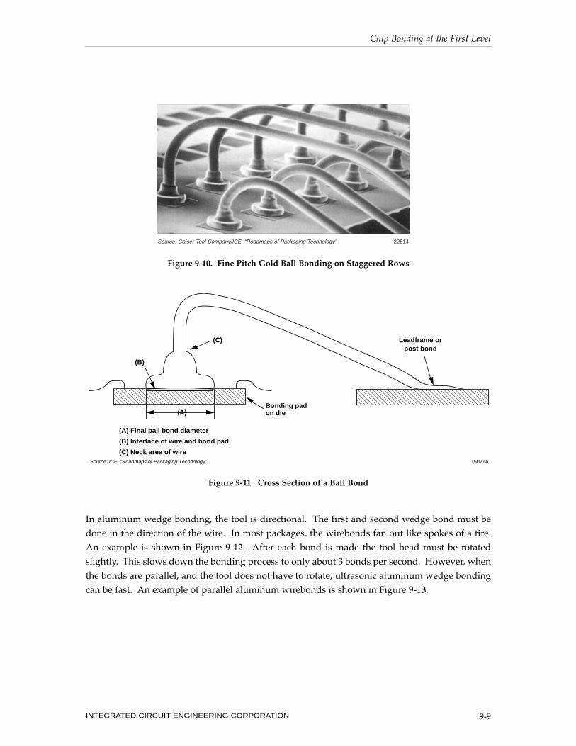
In aluminum wedge bonding, the tool is directional. The first and second wedge bond must be
done in the direction of the wire. In most packages, the wirebonds fan out like spokes of a tire.
An example is shown in Figure 9-12. After each bond is made the tool head must be rotated
slightly. This slows down the bonding process to only about 3 bonds per second. However, when
the bonds are parallel, and the tool does not have to rotate, ultrasonic aluminum wedge bonding
can be fast. An example of parallel aluminum wirebonds is shown in Figure 9-13.
Chip Bonding at the First Level
INTEGRATED CIRCUIT ENGINEERING CORPORATION 9-9
Source: Gaiser Tool Company/ICE, “Roadmaps of Packaging Technology” 22514
Figure 9-10. Fine Pitch Gold Ball Bonding on Staggered Rows
Figure 9-11. Cross Section of a Ball Bond
���������������������������������������������������������
���������������������������������������������������������
(C)
(B)
(A)
(A) Final ball bond diameter
(B) Interface of wire and bond pad
(C) Neck area of wire15021ASource: ICE, “Roadmaps of Packaging Technology”
Leadframe or post bond
Bonding padon die
Chip Bonding at the First Level
INTEGRATED CIRCUIT ENGINEERING CORPORATION9-10
Source: Electronic Design/ICE, “Roadmaps of Packaging Technology” 22409
Figure 9-12. Typical Wirebond Pattern with Fan Out From the Chip Pitchto the Package Bonding Shelf Pitch
Figure 9-13. 6mil Pitch Parallel Wirebonds to a Thin-Film Substrate
Source: Advanced Packaging Systems/ICE, “Roadmaps of Packaging Technology” 15910

On Chip Pad Pitch
All roads lead to increased pad count for die. This comes from the combination of increased func-
tionality and gate count, and the need for more power and ground pins to minimize ground
bounce. Yet, the die size for the same gate count is decreasing as the feature size gets smaller.
These factors contribute to the need to decrease the pad pitch required around the periphery of a
die for bonding pads.
For example, the Pentium chip has maintained the same functionality, yet has gone through a
number of die shrinks as the feature size has been reduced. The die shrink is illustrated in Figure
9-14. Though the die got smaller, the number of I/O off the die stayed the same. This means the
bond pad pitch has to shrink.
The IC manufacturing process can make pads on 1 micron centers. However, the useful pitch of
a bonding pad is set by the wirebonder technology. This is the major driving force on bonding
technology- allowing a tighter pad pitch on the chip.
Figure 9-15 illustrates the roadmap for finer pitch wirebonding in production, in the past and in
the future. In 1996, the tightest pitch in prototype production for ball or wedge bonding is roughly
70 microns. An example of 70 micron gold ball bonding is shown in Figure 9-16.
Chip Bonding at the First Level
INTEGRATED CIRCUIT ENGINEERING CORPORATION 9-11
0.8 Micron 0.5 Micron 0.35 Micron
Pentium(P5)
294 mm2 Pentium(P54C)
163 mm2
Pentium(P54CS)163 mm2
Source: Microprocessor Report/ICE, “Roadmaps of Packaging Technology” 20310
= CPU Core
= Pad Ring
Figure 9-14. Intel Shrinks Pentium

Chip Bonding at the First Level
INTEGRATED CIRCUIT ENGINEERING CORPORATION9-12
22515Source: Semiconductor International/ICE, "Roadmaps of Packaging Technology"
1996 1997 1998 1999
100µm
80µm
70µm
60µm
50µm
������
������������
������������
������Feasibility Prototype α-/β-Test Production
Without Recipe Transfer
With Recipe Transfer
Figure 9-15. Fine Pitch Roadmap
Figure 9-16. Bond Pitches of 70µm are Expected to Reach the Production Stage in Mid-1998
Source: ESEC/ICE, “Roadmaps of Packaging Technology” 22413

Figure 9-17 shows the maximum number of pads that can fit on a die with a fixed pad pitch. For
the largest die, at 18mm on a side, the pad limited I/O count is 720 I/O for 100 micron centers. A
growing concern for large ASICs is being pad limited. This means the die size must be artificially
increased to allow enough perimeter for all the bonding pads. The last thing a chip fabricator
wants to do is ship bare silicon on a chip in order to have enough periphery for all the bonding
pads. Getting around the Òtyranny of the peripheral bonding padsÓ is a major driving force for
area array flip chip.
Pitch on the First Level
The wirebond is the first step in the mechanical transformation from the die pitch to the package
pitch. It is only the most leading edge packages that can handle a pad pitch of the same dimen-
sion as the chip. In such a case, there is no fanout of the wirebonds, and they are all short and par-
allel. An example of a ceramic package with a thin film metallization layer on top, with a 6mil
pitch, matching the pitch on the chip, is shown in Figure 9-18.
Chip Bonding at the First Level
INTEGRATED CIRCUIT ENGINEERING CORPORATION 9-13
0 1
Nu
mb
er o
f P
ads
2 3 4 5 6 7 8
Die Size (mm)
9 1110 12 14 16 1813 15 17 19 20
1,100
1,000
900
800
700
600
500
400
300
200
100
0
100 micron pitch
75 micron pitch
Source: ICE, "Roadmaps of Packaging Technology" 22516
Figure 9-17. Maximum I/O Possible for Pad Limited Peripheral Die

When a multilayer substrate is used as the package, multiple bonding shelves can be used to shorten
the maximum wirebond length. Figure 9-19 shows a three shelf cofired ceramic package used for a
high speed ASIC, with parallel wirebonds. A more economical approach is to use two bonding
shelves in the package and a fan out of the wirebonds. An example is shown in Figure 9-20.
If there is no cavity, and the package is to be mounted Òcavity upÓ, there can still be multiple rows
of pads on the surface of the package. This complicates the loop heights required, but keeps the
wirebonds short. An example is shown in Figure 9-21.
Chip Bonding at the First Level
INTEGRATED CIRCUIT ENGINEERING CORPORATION9-14
Source: Narumi/ICE, “Roadmaps of Packaging Technology” 16108
Figure 9-18. Ceramic PGA with Thin-Film Layer (6mil Cavity Pitch)
Figure 9-19. Cavity Down, 476-Lead Ceramic PGA with Three Bonding Shelvesto Keep Wirebonds Short
Source: Semiconductor International/ICE, “Roadmaps of Packaging Technology” 22402

For leadframe based packages, where the lead count is typically less than 200, there is a growing
problem due to the shrinking die size. The inner lead pitch of the leadframe is limited to a
mechanical stamping process. The tightest pitch leadframe inner lead pitch is about 8mils, based
on a leadframe thickness of 4mils, but is more typically 10mils. The longest wirebonds length,
found in the corners, is illustrated in Figure 9-22.
Figure 9-23 shows graphically that when the die bond pitch is 4mils and the lead pitch is 10mils,
the longest wirebond is over 200mils, way beyond the safe limit. As a rule of thumb, the longest
wirebond length should be kept to less than 100x the wire diameter. Otherwise, there is the
danger of wirebonds sagging or shorting during the molding process.
As die size shrinks, this problem will get worse. One solution is to use an interposer in the cavity,
fabricated with a lithographic process that has a fine pitch to match the chip, and fans out to a
coarser pitch to match the leadframe.
Chip Bonding at the First Level
INTEGRATED CIRCUIT ENGINEERING CORPORATION 9-15
Source: Kyocera/ICE, “Roadmaps of Packaging Technology” 22517
Figure 9-20. Example of Ceramic PGA with Two Bonding Shelves
Figure 9-21. Multiple Bonding Rows on the Same Level
Source: K&S/ICE, “Roadmaps of Packaging Technology” 22518
DieG/S
Core Material
Standard Loop
BGA Loop
Worked Loop
G/S Lead

Chip Bonding at the First Level
INTEGRATED CIRCUIT ENGINEERING CORPORATION9-16
Pinner
Pinner •Npads
8
Pouter
•Npads
8Pouter
Llongest
=Llongest 2 Npads8 Pouter( 1 )• – Npads8 Pinner1
•
=2 (
= 0.18
8Npads Pouter Pinner– )
(Npads Pouter Pinner– )15842Source: ICE, “Roadmaps of Packaging Technology”
Figure 9-22. Longest Wirebond
Figure 9-23. Largest Wirebond for Different Inner Lead Pitches and a 4mil Pad Pitch on the Chip
0 100 200 300 400 500
Number of I/O
Max
imu
m W
ireb
on
d L
eng
th (
in m
ils)
600 700 800 900 1,000
600
500
400
300
200
100
0
Source: ICE, “Roadmaps of Packaging Technology” 22519
10mil Inner Lead Pitch
8mil Inner Lead Pitch
6mil Inner Lead Pitch

CHIP PAD BONDING: FLIP CHIP
Using the surface of the die for I/O by definition requires the die to be mounted face to face with
the interconnect substrate. This is usually viewed as flipped from the conventional pads-up ori-
entation, and hence the name, flip chip. The use of the entire surface of the die for interconnect
opens many new possibilities for both single- and multi-chip applications.
Driving Forces for Flip Chip
There are five major advantages with an area array format for chip pads:
¥ Enabling higher I/O possible off a fixed sized die
¥ Lower cost die by allowing a smaller sized die in a pad limited design
¥ Lower switching noise due to more power and ground pads and lower lead inductance
¥ Smaller footprint possible on the substrate enabling new product form factors
¥ Lower assembly costs by batch bonding and avoiding the extra cost of a package
It is usually one or more of these features which has motivated the tremendous interest in flip chip
approaches in the last 5 years and contributed to the proliferation of possible implementation paths.
The fundamental motivation for flip chip attach is to allow an area array distribution of I/O off a
chip. Even using conservative design rules of 10mil centers to the area array interconnections, the
I/O count is very large compared to peripheral attach methods. For example, on a moderate sized
die of 15mm on a side, over 5,000 connections would be available. This means either a fixed die
size can get more I/O, or a fixed I/O can be fit on a smaller die.
Figure 9-24 illustrates the I/O count possible using a 10mil pitch area array and a 4mil and 3mil
pitch peripheral I/O. For pad limited die larger than 100 I/O, an area array form factor will yield
a smaller die than 4mil pitch peripheral pads.
Another motivation for flip chip assembly is as an implementation of chip scale packaging (CSP).
This means the package footprint on the substrate takes up no more than an additional 20% real
estate over the bare chip physical size. This is a huge system level density advantage. In some
cases, it can save in product size and assembly costs.
Another motivation for flip chip is in the lower possible bonding parasitics and better electrical
performance. The typically short length of the flip chip bonds translates directly into less power
and ground inductance. Other advantadges include higher potential pad count for power and
ground pads and flexible positioning over the surface of the die will also decrease the impedance
of the power and ground distribution network.
Chip Bonding at the First Level
INTEGRATED CIRCUIT ENGINEERING CORPORATION 9-17

Flip Chip for Single Chip Packages
Though flip chip attach is a popular method for implementing MCMs, it is also being used in
single chip packages, primarily when the die is pad limited. A smaller die is possible using area
array off the die. This translates to a cost reduction in the silicon over wirebonding. In addition,
with shorter bond lengths, there is less switching noise which can contribute to a performance
gain. Both of these features make flip chip attractive for very high pin count die, typically greater
than 500 pins, in single chip packages.
In 1996, flip chip (FC) single chip applications almost exclusively used ceramic substrates, either
CQFP or CBGA. An example is shown in Figure 9-25. Multilayer, cofired ceramic is required pri-
marily because of the tighter via pitch needed to route the escapes from the closely spaced solder
balls on the die, and because of the established reliability database for use in flip chip applications.
An underfill is used to provide enhanced reliability from thermal cycling and environmental pro-
tection for the flip chip die.
As microvia technology moves into production for laminate technology, PCBs will increasingly be
used as the substrate of choice. An example of a flip chip PCB single chip package is shown in
Figure 9-26.
Chip Bonding at the First Level
INTEGRATED CIRCUIT ENGINEERING CORPORATION9-18
Source: ICE, "Roadmaps of Packaging Technology" 22520
0 1 2 3 4 5 6 7 8 9 10 11 12 13 14 15 16 17 18 19 20
10,000
1,000
100
10
Pad
Lim
ited
I/O
Co
un
t
Die Size (mm)
4mil pitch
3mil pitch
10mil grid array
Figure 9-24. Number of I/O Possible if Pad Limited for Peripheral and Area Array Pads

Chip Bonding at the First Level
INTEGRATED CIRCUIT ENGINEERING CORPORATION 9-19
Source: IBM/ICE, “Roadmaps of Packaging Technology” 22122
Figure 9-25. Single Chip Ceramic Package with Flip Chip Assembly
Figure 9-26. Flip Chip on Single Chip Laminate Package
Source: LSI Logic/ICE, “Roadmaps of Packaging Technology” 22123

The same issues related to designing and implementing flip chip assembly applies for both single
chip and multiple chip packages. Applications for flip chip in multi-chip packages are described
in a later chapter.
Assembly Process: Solder Attach
There are two fundamental methods that are used in production to attach flipped chip devices to
the next level: solder and conductive adhesives.
Flip chip attach with solder has been in use since the Ô60Õs by IBM for computers and Delco
Electronics for automotive applications. The early process involved the evaporation through a
shadow mask of a 97% Pb/3% Sn high temperature solder to the conditioned die. The solder was
reflowed on the chip to form a solder ball. The bumped chip was then flip chip attached to a
ceramic substrate. This assembly was reflowed at the 350¡C melt point and the solder ball collapsed
to form a squashed tomato shape. This process of controlled collapse chip connection was termed
C4. In 1996, Delco alone performed 300,000 flip chip assemblies per day, with a variant of C4.
Figure 9-27 shows the cross section of a flip chip die attached to the substrate. Though there is a
wide variation in the specifics of the processes, the basic steps to prepare a chip and attach it to a
surface with solder are the same. The basic features are:
¥ Aluminum pad metallization
¥ under bump metallization (UBM)
¥ solder bump
¥ pad on the substrate
¥ underfill polymer
Chip Bonding at the First Level
INTEGRATED CIRCUIT ENGINEERING CORPORATION9-20
Source: Fujitsu Computer Packaging Technology/ICE, “Roadmaps of Packaging Technology” 22552
900 Ball Flip Chip ASIC Close Up of the 5mil Diameter SolderBalls on the ASIC
Cross Section of Solder BallShowing the UBM on the ASIC
Figure 9-27. Solder Ball Flip Chip ASIC

The basic process steps, with their variants are listed in Figure 9-28.
In the original C4 process, the solder ball was a high melting point solder. Virtually all the con-
nections were made to a ceramic substrate, and the solder ball was reflowed to the substrate at
about 350¡C to form the controlled collapse joint.
In applications for attach to polymer substrates, two approaches have been adopted. First is to
use a eutectic solder ball on the chip, and reflow at about 200¡C to attach the chip to the board.
The second approach is to use the high lead solder ball on the chip, but eutectic solder paste on
the board, and reflow the chip at 200¡C. The solder on the board will melt and reflow, forming a
joint to the high temperature solder ball. In this case, the high Pb solder ball is acting as a solder-
able standoff. This is the process Motorola uses for consumer product applications of direct chip
attached flip chips on FR-4 substrates.
The final step in the flip chip assembly process is to underfill the chip with a stress relieving poly-
mer. Due to thermal mismatches between the silicon chip and the substrate, there will be stresses
applied to the solder balls. Typically, the balls farthest from the neutral pointÑthe centerÑwill
experience the highest stresses. During thermal cycling, the periodic stress on the solder joints
will eventually initiate and propagate cracks which result in joint failures.
Chip Bonding at the First Level
INTEGRATED CIRCUIT ENGINEERING CORPORATION 9-21
Source: ICE, "Roadmaps of Packaging Technology" 22550
• design the I/O for area array fromthe beginning
• redistribute the traditional peripheralpads to area array pads with one ortwo metal layers deposited on thewafer
• adhesion layers: Cr, Ti
• solder wetting layer: Ni, Cu
• solderable protective surface: Au,solder
• evaporate, electroplate
• solder composition: Pb/Sn 97/3,95/5, 63/7, 60/40
• reflow
• screen print solder paste and flux
• solder plate and apply flux
• pick and place SMT equipment
• locally heated
• reflow oven
• snap cured, low viscosity epoxy
create area array pads
build the solder ball
metallization for solder: under bumpmetallization (UBM)
align and place flipped chip to substrate
prepare pad on substrate
reflow the solder and form the joint
underfill polymer
Figure 9-28. Basic Process for Chip Attach with Solder

The greater the thermal expansion mismatch, the fewer thermal cycles before failure. The relative
number of cycles before onset of failure is described by the Coffin-Manson equation. This is shown
graphically in Figure 9-29. The use of ceramic substrates with flipped chips results in a large
number of cycles before failure. When FR-4 is used, the fatigue life is reduced by a factor of 100.
To gain back the long life reliability, the 3-5mil gap underneath the chip can be underfilled with a
stress relieving polymer, usually low viscosity epoxy. The liquid epoxy is dispensed around two
or three sides of the flipped chip and capillary forces are used to draw the liquid under the die.
This is shown in Figure 9-30.
Figure 9-31 illustrates the cycles to failure of a flip chip on FR-4 with and without the underfill.
Without the underfill, 50% of devices will show solder joint failures within 5 thermal cycles. With
the underfill, the devices can withstand over 1000 thermal cycles. The polymer distributes the
stress more evenly over the surface of the silicon chip, rather than concentrating it at the outer-
most solder joints.
Chip Bonding at the First Level
INTEGRATED CIRCUIT ENGINEERING CORPORATION9-22
Glass-Ceramic
Polyimide-Kevlar
Polyimide-Kevlar
Alumina Ceramic
Epoxy-Kevlar
Polyimide-Glass
Epoxy-Glass
100
0
1,000
10,000
100,000
0 40 80 120 160 200 240
1/γ2 Coffin-Manson Equation
Fati
gu
e L
ife-
Cyc
les
N50
Coefficient of Thermal Expansion (10-7/°C)
Source: Tummala/ICE, “Roadmaps of Packaging Technology” 22124
Figure 9-29. Influence of Board Expansivity on Thermal Cycle Lifetime of Solder Joint

The underfill polymer has an added function of providing environmental protection and
enhanced thermal conductivity from the chip to the substrate. Just as a polymer encapsulant
enabled the introduction of wirebonded COB applications, the underfill polymer enables the use
of flip chip attach on laminate substrates, a major cost advantage.
Chip Bonding at the First Level
INTEGRATED CIRCUIT ENGINEERING CORPORATION 9-23
Source: Asymtek/ICE, “Roadmaps of Packaging Technology” 22125
Figure 9-30. Application of Underfill Epoxy to Flip Chip Mounted to Ceramic Package
Figure 9-31. Fatigue Life Data of Flip Chip to FR-4 With and Without Underfill,for Different Gap Heights
100
80
60
40
20
01 10 100 1,000 10,000
Cu
mm
ula
tive
Fai
lure
%
Thermal Cycles
30µm
30µm
50µm
h=80µm
80µm
Source: Toshiba/ICE, "Roadmaps of Packaging Technology" 22126
No Underfill
WithUnderfill

Wafer Bumping Costs
The process of preparing the wafer with the necessary metallization and solder balls is called
wafer bumping. The cost to bump a wafer is extremely sensitive to the process steps and lithog-
raphy requirements. The proliferation of different processes to end up with a bumped wafer is
driven by the need to get around patent protections and to find paths to decrease the wafer bump-
ing costs.
The street price for wafer bumping is about $250/6 inch wafer, in low volume. A cost analysis by
MCNC is shown in Figure 9-32. They predict that for low volume bumping, the cost should be
about $100/wafer. They estimate that the cost should be as low as $10/wafer, in high volume
production.
MCNC has spun off a company, Unitive, to commercialize their wafer bumping process, as a mer-
chant contract bumping service provider. Recently, Delco Electronics, and Kulicke and Soffa
formed a joint venture named Flip Chip Technologies, another merchant supplier of wafer bump-
ing services. Delco has over 25 years of wafer bumping and flip chip experience, and K&S is the
worldÕs largest supplier of wirebonding equipment. This new joint venture is setting up manu-
facturing capacity to bump 1.5 million devices per day.
Chip Bonding at the First Level
INTEGRATED CIRCUIT ENGINEERING CORPORATION9-24
700
600
500
400
300
200
100
0
1993 1994 1995 1996 1997 1998 1999 2000
Low Volume BumpingLow Volume Redistribution & BumpingLow Volume 2-Level RedistributionHigh Volume BumpingHigh Volume Redistribution & BumpingHigh Volume 2-Level Redistribution
Source: Semiconductor Technology Center/ICE, “Roadmaps of Packaging Technology” 22127
Do
llars
Per
Waf
er
Year
Figure 9-32. Cost of Ownership Modeling for MCNCÕs Solder Bumping Process

Wafer bumping is a batch process. The costs are based on wafer size, not number of pads on the
wafer. Flip chip attach can offer a cost reduction over wirebonding if a large enough number of
pads are bumped at one time. The more pads on a wafer, the lower the per-pad cost. The number
of pads on a wafer depends on the area of the wafer, the length of the side of a chip, and the pad
pitch if they are on the periphery and the chip is pad limited in I/O. The number of pads on a
wafer is given by:
The number of pads increases as the chip size gets smaller, or the pad pitch gets smaller. For
example, with a 10mm chip, and pad pitch of 100 microns, there are a total of 400 pads per die.
On a 150mm round wafer, about 150 chips can be placed. If the yield is very high, there would be
over 60,000 solder bumped pads. At $100 cost to bump the wafer, the cost per pad is $0.0015. This
cost drops even lower, with a smaller die. This is to be compared with a wirebond cost of about
$0.005, in high volume.
As the infrastructure grows for wafer bumping and substrate fabrication, flip chip offers the pos-
sibility of future assembly cost reductions, even for single chip packages.
Unconventional Approaches to Flip Chip Solder Attach
In addition to the conventional processes above, some novel variations have been proposed.
The most expensive wafer bumping step is the lithography process used to either redistribute the
peripheral pads to area array or to pattern the UBM to define the solder bump pads. Two meth-
ods have been proposed to implement solderable standoffs on the chip without lithography.
The first method uses an electroless zincate process to activate the aluminum pad with zinc, which
can then be electrolessly plated with nickel and then copper or gold. The process steps are shown
in Figure 9-33. The entire process of transforming a flat aluminum pad into a gold plated bump
is done entirely electroless, basically dipping the wafer in various solutions. Figure 9-34 is a cross
section of an electrolessly grown bump. To attach the chip to a substrate, solder would have to be
screen printed to the substrate.
The second method uses a modification of the standard gold ball bonding process. After all, in
gold ball bonding, a gold wire is metallurgically attached to an aluminum pad, without using any
lithographic steps or additional chemistry. In the standard process, a gold ball is formed on the
end of the wire and is thermosonically attached to the aluminum pad. The wire is then drawn up
and looped to a second pad location. If the wire is broken before it loops up very high, a gold ball
and stud are left on the chip.
N
AL
4L
P4AL Ppads on wafer
wafer
Chip2
chip
chip
wafer
chip chip
= • =
Chip Bonding at the First Level
INTEGRATED CIRCUIT ENGINEERING CORPORATION 9-25

There are a number of variations on this theme, each with a different amount of wire left behind,
from no stud to a 20mil stud.
Chip Bonding at the First Level
INTEGRATED CIRCUIT ENGINEERING CORPORATION9-26
��������������������
��������������������
��������������������
��������������������
��������������������
Source: IEEE Transactions on Components,Packaging, and Manufacturing Technology/ICE, “Roadmaps of Packaging Technology”
22128
Al Bonding Pad Oxide PassivationSiO
Pretreatment(Zincate)
ElectrolessNiP
Electroless Cu
Protective Layer (Au, Sn)
Silicon
Figure 9-33. Schematic of the Electroless Zincate Bumping Process
Figure 9-34. Metallographic Cross Section of a Nickel/Copper/Tin Bump
Source: IEEE Transactions on Components, Packaging, and Manufacturing Technology/ICE, “Roadmaps on Packaging Solutions”
22129
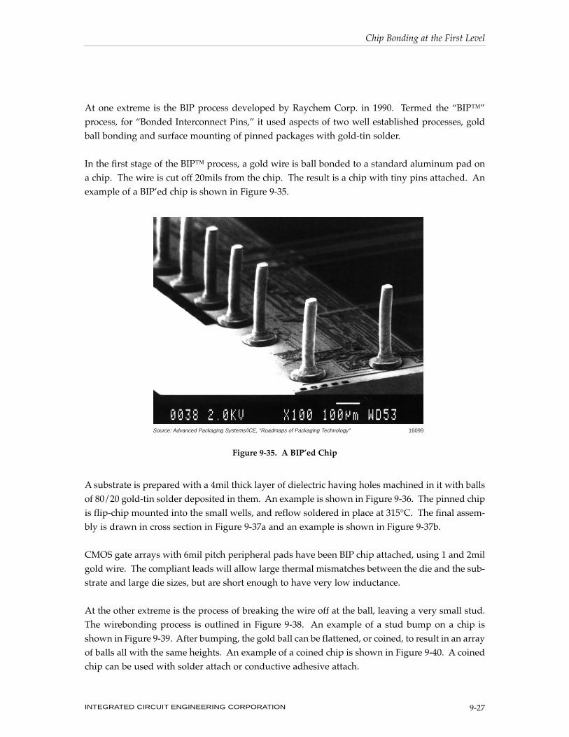
At one extreme is the BIP process developed by Raychem Corp. in 1990. Termed the ÒBIPªÓ
process, for ÒBonded Interconnect Pins,Ó it used aspects of two well established processes, gold
ball bonding and surface mounting of pinned packages with gold-tin solder.
In the first stage of the BIPª process, a gold wire is ball bonded to a standard aluminum pad on
a chip. The wire is cut off 20mils from the chip. The result is a chip with tiny pins attached. An
example of a BIPÕed chip is shown in Figure 9-35.
A substrate is prepared with a 4mil thick layer of dielectric having holes machined in it with balls
of 80/20 gold-tin solder deposited in them. An example is shown in Figure 9-36. The pinned chip
is flip-chip mounted into the small wells, and reflow soldered in place at 315¡C. The final assem-
bly is drawn in cross section in Figure 9-37a and an example is shown in Figure 9-37b.
CMOS gate arrays with 6mil pitch peripheral pads have been BIP chip attached, using 1 and 2mil
gold wire. The compliant leads will allow large thermal mismatches between the die and the sub-
strate and large die sizes, but are short enough to have very low inductance.
At the other extreme is the process of breaking the wire off at the ball, leaving a very small stud.
The wirebonding process is outlined in Figure 9-38. An example of a stud bump on a chip is
shown in Figure 9-39. After bumping, the gold ball can be flattened, or coined, to result in an array
of balls all with the same heights. An example of a coined chip is shown in Figure 9-40. A coined
chip can be used with solder attach or conductive adhesive attach.
Chip Bonding at the First Level
INTEGRATED CIRCUIT ENGINEERING CORPORATION 9-27
Source: Advanced Packaging Systems/ICE, “Roadmaps of Packaging Technology” 16099
Figure 9-35. A BIPÕed Chip

Chip Bonding at the First Level
INTEGRATED CIRCUIT ENGINEERING CORPORATION9-28
Source: Advanced Packaging Systems/ICE, “Roadmaps of Packaging Technology” 16100
Figure 9-36. Solder Balls in 6mil Holes for BIPÕed Chip
Figure 9-37. The BIPÕed Chip Showing Basic Structure and on a Substrate
Source: Advanced Packaging Systems/ICE, “Roadmaps of Packaging Technology” 22216
Chip
BIP™(Bonded Interconnect Pin)
Solder Well
Solder Pad
Substrate
Top DielectricLayer
a
b

An intermediate version of this process is the BIT (Bonded Interconnection Technology) process
from Fujitsu. A small stud is left protruding from the gold ball, which is used to provide a higher
standoff, after either adhesive attach or solder attach to the substrate. A cross section is shown in
Figure 9-41.
Chip Bonding at the First Level
INTEGRATED CIRCUIT ENGINEERING CORPORATION 9-29
����������������������������������������
������������������������������������������������
����������������
����������������
������������������������
������������������������
������������������������
������������������������
CapillaryTube
GoldWire
Ball Formation ThermocompressionBonding
Movement Wire Cutting
StudBump
19377Source: ICEMM Proceedings '93/ICE, "Roadmaps of Packaging Technology"
Figure 9-38. Single-Bump Gold Ball Bond Process
Figure 9-39. SEM Micrograph of Gold Bumps on a Die
Source: nCHIP/ICE, “Roadmaps of Packaging Technology” 22131

An extreme example of the use of narrow, fine pitch wires for flip chip attach is the WIT (wire inter-
connect technology) process from Fujitsu Computer Packaging Technology. By the use of electro-
less copper plated through high aspect ratio holes in photoresist, 40 micron tall, 10 micron diameter
copper wires can be grown on pads. Wires on a 45 micron pitch have been demonstrated. An
example is shown in Figure 9-42. On a chip 10mm on a side, this would allow a staggering 40,000
I/O! Of course, there are no substrates currently available that can interconnect all these I/O.
Assembly Process: Adhesive Attach
Another approach to implementing flip chip technology relies on the use conductive adhesives.
They can be either isotropically conductive or anisotropically conductive materials.
Chip Bonding at the First Level
INTEGRATED CIRCUIT ENGINEERING CORPORATION9-30
Source: Gaiser Tool Company/ICE, “Roadmaps of Packaging Technology” 22524
Figure 9-40. Chip with Peripheral Coined Bumps and Close Up of a Coined Bump
Figure 9-41. Bonded Interconnection Technology (BIT)
Source: Fujitsu Computer Packaging Technology/ICE, “Roadmaps of Packaging Technology” 22553
������������������������������������������������������������������������������������������������������������������������������������������������������������������������������������������������������������������������
Mother Board
Au BumpConductive Paste
Adhesive
Bare Chip
Diagram of BIT : Bonded Interconnection T echnology Actual Cross Section of BIT Chip Attached toLaminate Substrate

Isotropically conductive adhesives are typically epoxy based, and filled with conductive particles,
commonly silver, nickel or tin. As the loading concentration of the filler material increases, the
bulk resistivity drops dramatically. Figure 9-43 shows the transition from 1014 Ohm-cm, the bulk
resistivity of the epoxy base, to about 1 Ohm-cm, when the Nickel concentration is increased from
30% to 60%.
Chip Bonding at the First Level
INTEGRATED CIRCUIT ENGINEERING CORPORATION 9-31
Courtesy of Fujitsu Computer Packaging TechnologySource: ICE, “Roadmaps of Packaging Technology 22526
Figure 9-42. Sea of WITs
Figure 9-43. Resistivity Versus Nickel Volume Concentration in Polymer Matrix
20 30 40 50 60 70
1E14
1E8
1E2
1
Res
isti
vity
(O
hm
-m),
Lo
g S
cale
Nickel Volume Concentration (%)Source: IEEE Transactions on Components, Hybrids, and Manufacturing Technology/
ICE, “Roadmaps of Packaging Technology”22135
These conductive filled polymers have historically been used extensively in die attach applica-
tions, and have recently been applied to chip bonding applications. Epoxy Technology has coined
the term Polymer Flip Chip (PFC) to refer to bumping of die with isotropically conductive poly-
mer, and the subsequent lack of solder bonding to the next level.
The aluminum pads on the IC die are not stable surfaces to contact the conductive epoxy. The
native oxide present prevents a good ohmic contact. Contact resistances can be on the order of
100 Ohms and break through voltages, depending on the oxide thickness, can be 2-7 volts. The
first step in using a conductive adhesive is to bump the die with an inert metal. An attractive
process that is potentially low cost is the electroless zincate process, described above. This is a
maskless process involving the electroless plating of first a thin zinc layer, followed by a nickel
layer and finally capped with a gold layer.
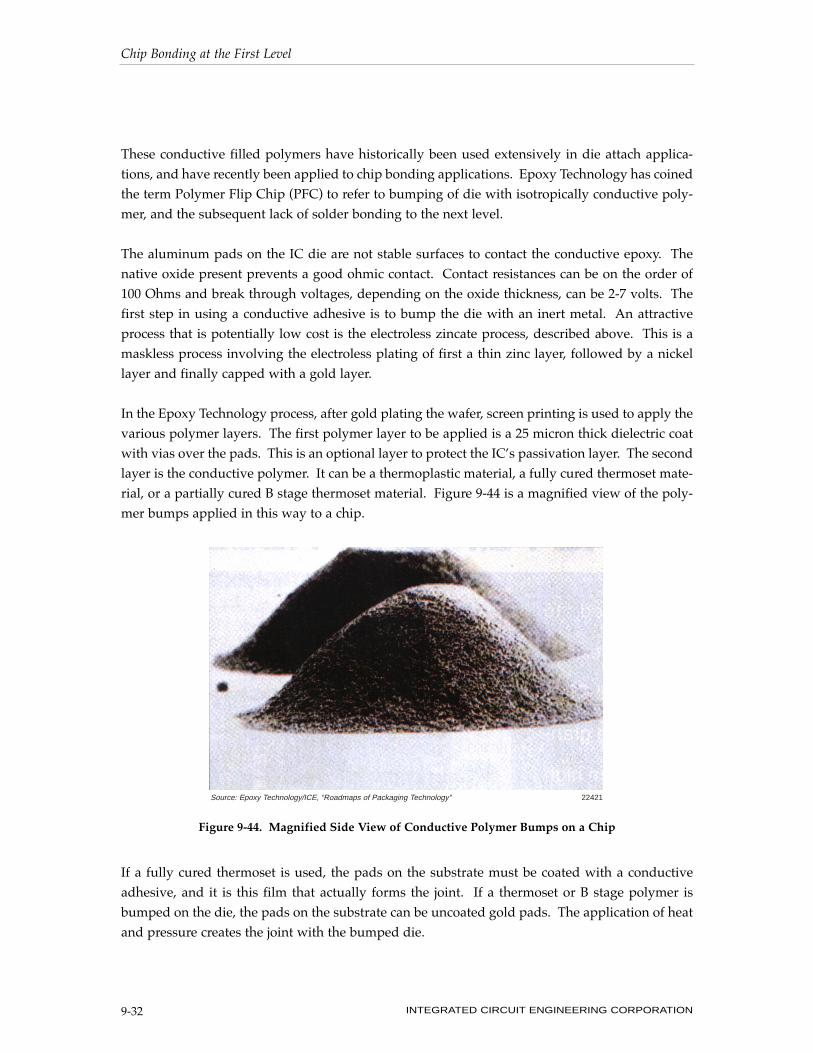
In the Epoxy Technology process, after gold plating the wafer, screen printing is used to apply the
various polymer layers. The first polymer layer to be applied is a 25 micron thick dielectric coat
with vias over the pads. This is an optional layer to protect the ICÕs passivation layer. The second
layer is the conductive polymer. It can be a thermoplastic material, a fully cured thermoset mate-
rial, or a partially cured B stage thermoset material. Figure 9-44 is a magnified view of the poly-
mer bumps applied in this way to a chip.
If a fully cured thermoset is used, the pads on the substrate must be coated with a conductive
adhesive, and it is this film that actually forms the joint. If a thermoset or B stage polymer is
bumped on the die, the pads on the substrate can be uncoated gold pads. The application of heat
and pressure creates the joint with the bumped die.
Chip Bonding at the First Level
INTEGRATED CIRCUIT ENGINEERING CORPORATION9-32
Source: Epoxy Technology/ICE, “Roadmaps of Packaging Technology” 22421
Figure 9-44. Magnified Side View of Conductive Polymer Bumps on a Chip

After flip chip attach, the chip can be underfilled with a low stress polymer for mechanical and
environmental protection.
An alternative approach, used by Fujitsu in their BIT process, for example, uses gold ball bonding
as the method of bumping the wafer. The gold posts on each pad are coated with a thin layer of
silver filled epoxy by touching the die surface to a screen printed film of the epoxy. The silver
filled epoxy is picked up by only the protruding gold bumps. An example of the gold studs
coated with the conductive epoxy prior to substrate attach is shown in Figure 9-45. This adhesive
is used to make the mechanical and electrical contact between the chip and the gold pads of the
substrate to which it is bonded.
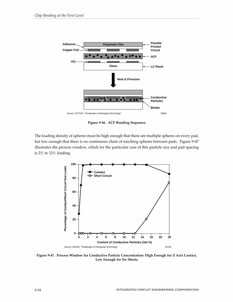
The use of anisotropically conductive polymers has been popular in the LCD display industry for
many years, but may not transfer to the general purpose digital world. The principle of an
anisotropically conductive adhesive is illustrated in Figure 9-46.
These materials consist of an insulating matrix, such as an epoxy, filled with small, uniform sized
latex spheres, coated with a thin layer of Nickel and gold. The loading density of the spheres is
low, typically less than 15%. This adhesive is placed between the pads of the die and the match-
ing pads of the substrate. When the die is pressed against the substrate, some of these spheres
are trapped between the pads and are compressed.
Chip Bonding at the First Level
INTEGRATED CIRCUIT ENGINEERING CORPORATION 9-33
Courtesy of Fujitsu Computer Packaging Technology/ 22527Source: ICE, “Roadmaps of Packaging Technology”
Figure 9-45. BIT Studs After Coating with Conductive Epoxy
The loading density of spheres must be high enough that there are multiple spheres on every pad,
but low enough that there is no continuous chain of touching spheres between pads. Figure 9-47
illustrates the process window, which for the particular case of this particle size and pad spacing
is 2% to 12% loading.
Chip Bonding at the First Level
INTEGRATED CIRCUIT ENGINEERING CORPORATION9-34
Heat & Pressure
Polyimide Film
Glass
FlexiblePrintedCircuit
ACF
ITO
Adhesive
Copper Foil
LC Panel
ConductiveParticles
Binder
Source: SST/ICE, “Roadmaps of Packaging Technology” 20964
Figure 9-46. ACF Bonding Sequence
Figure 9-47. Process Window for Conductive Particle Concentration: High Enough for Z Axis Contact,Low Enough for No Shorts
100
80
60
40
20
00 2 4 6 8 10 12 14 16 18 20
ContactShort Circuit
Content of Conductive Particles (Vol %)
Per
cen
tag
e o
f C
on
tact
/Sh
ort
Cir
cuit
Tes
t L
ead
s
Source: Oki/ICE, "Roadmaps of Packaging Technology" 22138
Many variations on this principle are possible. When the conductive adhesive is applied as a film
the process is termed ACF (anisotropically conductive film). The polymer can be a thermoset or
UV curable polymer. For LCD applications, the chip is typically mounted to a glass substrate, and
the UV can be projected through the glass substrate.
The chief limitation with all of these approaches is the relatively high contact resistance of the joint,
and low current carrying capacity. Contact resistances can be on the order of 1 Ohm, and current
carrying capacity can be limited to under 100mA per pad. These features will limit the applica-
tion of this technique for digital interconnects, but pose no limitation for LCD interconnects.
Challenges for Flip Chip
With the wonderful benefits of flip chip attach, it is useful to ask why it is not used more. There
are three fundamental reasons.
First, there is inertia. There is risk involved in changing a process that works. If a compelling,
enabling, or cost advantage does not exist, the conventional methods will continue to be used.
Second is the requirements on the substrate. As pointed out in early chapters, to interconnect and
route the high density of pads requires a substrate with both fine lines, and for high pin count
chips, a high via density. This means expensive substrates such as cofired ceramic or microvia
PCBs. The total cost of ownership may be too high for many applications.
Finally, the infrastructure for flip chip attach is still young. The four highest volume users, IBM,
Motorola, Delco and AT&T, have implemented and taken responsibility for the infrastructure
themselves. It will take more time for this infrastructure to propagate into the commercial mer-
chant market.
However, even given these barriers, the risk takers are switching to flip chip. At the high end, die
with a large number of I/O are being implemented in flip chip to gain the highest performance,
at a cost savings over wirebond.
At the low end, small chips are being implemented in consumer applications as DCA onto lami-
nate substrates to get the smallest possible form factors.
It is estimated that the number of flip chip devices is increasing at the rate of 38% per year, and
will continue to grow at this rate through the year 2000. This opportunity will motivated the
growth of the merchant infrastructure.
Chip Bonding at the First Level
INTEGRATED CIRCUIT ENGINEERING CORPORATION 9-35

TAB (TAPE AUTOMATED BONDING)
ÒTAB is entering its third decade of being the technology of the future.Ó
Ñ B.E. Kurtz, Allied-Signal, 1990
It has often been said that TAB is the only way of implementing fine-pitch pads. It is currently in
production for 3.5mil inner lead bonds on the Pentium TCP (tape carrier package). An example
of a TAB leadframe with 3mil pitch is shown in Figure 9-48. Two mil pitch TAB bonding has been
demonstrated in the lab.
There are many strategies for implementing TAB, depending on whether the chip is specially pre-
pared, and whether the inner leads are gang bonded. Figure 9-49 describes the various options.
For example, the MCAIII chip is gold bumped and the inner leads of tinned copper form a gold-
tin bond. Hewlett-Packard TAB bonds to the aluminum pads of a chip with no special prepara-
tion, using a gold-plated leadframe and single point bonding.
The metallurgy associated with TAB attach is complicated. Ultimately, aluminum pads on the
chip are attached to solder or gold pads on the substrate with a copper core leadframe going
between them. On the bond on the chip, the metallurgy is gold-gold, aluminum-gold, gold-tin, or
solder-solder. The precise time-temperature-pressure conditions at which the joint is formed will
influence the intermetallics that form and the resulting reliability. This means very careful atten-
tion to the details of the manufacturing process is criticalÑall the more so when the inner leads
are gang bonded. These manufacturing challenges have contributed to the slow acceptance of
TAB in the U.S.
Chip Bonding at the First Level
INTEGRATED CIRCUIT ENGINEERING CORPORATION9-36
Source: Motorola/ICE, “Roadmaps of Packaging Technology” 16055
Figure 9-48. SEM of ILB Test Chip with 3mil Pitch (Gold Bumped Pads)
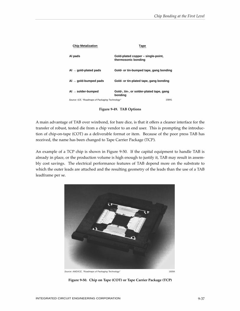
A main advantage of TAB over wirebond, for bare dice, is that it offers a cleaner interface for the
transfer of robust, tested die from a chip vendor to an end user. This is prompting the introduc-
tion of chip-on-tape (COT) as a deliverable format or item. Because of the poor press TAB has
received, the name has been changed to Tape Carrier Package (TCP).
An example of a TCP chip is shown in Figure 9-50. If the capital equipment to handle TAB is
already in place, or the production volume is high enough to justify it, TAB may result in assem-
bly cost savings. The electrical performance features of TAB depend more on the substrate to
which the outer leads are attached and the resulting geometry of the leads than the use of a TAB
leadframe per se.
Chip Bonding at the First Level
INTEGRATED CIRCUIT ENGINEERING CORPORATION 9-37
Al pads Gold-plated copper – single-point,thermosonic bonding
Al → gold-plated pads Gold- or tin-bumped tape, gang bonding
Al → gold-bumped pads Gold- or tin-plated tape, gang bonding
Al → solder-bumped Gold-, tin-, or solder-plated tape, gangbonding
Chip Metalization Tape
Source: ICE, "Roadmaps of Packaging Technology" 15841
Figure 9-49. TAB Options
Figure 9-50. Chip on Tape (COT) or Tape Carrier Package (TCP)
Source: AMD/ICE, “Roadmaps of Packaging Technology” 16094

It is often said that the inductance of TAB leads is lower than that of wirebonded leads. This
depends very strongly on the specific case. It is very possible for a wirebond lead to have an
inductance much less than a TAB lead. The inductance of wirebonds 50mils long is less than 1nH.
For a TAB fanout that goes from a 6mil inner lead pitch to a 20mil outer lead pitch, such as a
TapePak, the length of a trace can be over 0.5 inch long. Its inductance would be almost 10x the
wirebond example.
Chip Bonding at the First Level
INTEGRATED CIRCUIT ENGINEERING CORPORATION9-38