8-channel, 625 ksps, 12-bit parallel adcs with a … 625 ksps, 12-bit parallel adcs with a sequencer...
TRANSCRIPT
8-Channel, 625 kSPS, 12-Bit Parallel ADCs with a Sequencer
Data Sheet AD7938-6
Rev. E Document Feedback Information furnished by Analog Devices is believed to be accurate and reliable. However, no responsibility is assumed by Analog Devices for its use, nor for any infringements of patents or other rights of third parties that may result from its use. Specifications subject to change without notice. No license is granted by implication or otherwise under any patent or patent rights of Analog Devices. Trademarks and registered trademarks are the property of their respective owners.
One Technology Way, P.O. Box 9106, Norwood, MA 02062-9106, U.S.A. Tel: 781.329.4700 ©2004–2018 Analog Devices, Inc. All rights reserved. Technical Support www.analog.com
FEATURES Throughput rate: 625 kSPS Specified for VDD of 2.7 V to 5.25 V Power consumption 3.6 mW maximum at 625 kSPS with 3 V supplies 7.5 mW maximum at 625 kSPS with 5 V supplies 8 analog input channels with a sequencer Software-configurable analog inputs
8-channel single-ended inputs 4-channel fully differential inputs 4-channel pseudo differential inputs 7-channel pseudo differential inputs
Accurate on-chip 2.5 V reference ±0.2% maximum at 25°C, 25 ppm/°C maximum 69 dB SINAD at 50 kHz input frequency No pipeline delays High speed parallel interface with word/byte modes Full shutdown mode: 2 µA maximum 32-lead LFCSP and TQFP packages
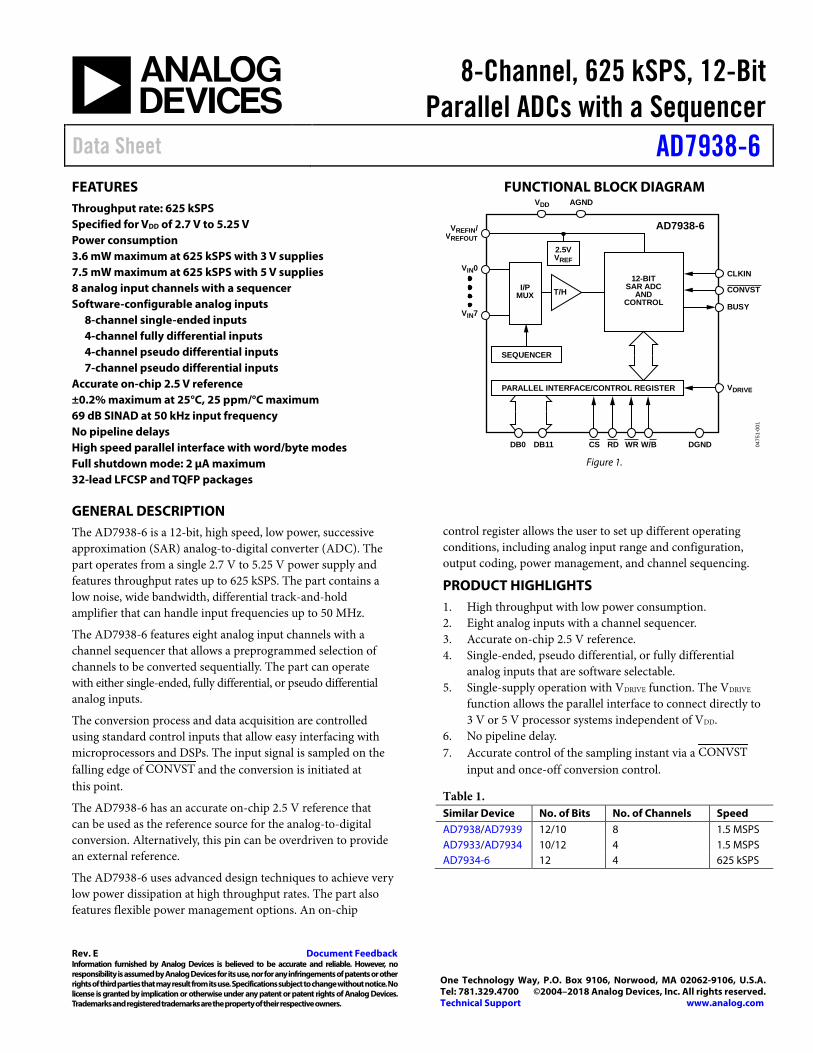
FUNCTIONAL BLOCK DIAGRAM
0475
1-00
1
VIN7
T/H
PARALLEL INTERFACE/CONTROL REGISTER
SEQUENCER
12-BITSAR ADC
ANDCONTROL
I/PMUX
2.5VVREF
DB0 DB11
VDRIVE
VDD
AD7938-6
VIN0
AGND
VREFIN/VREFOUT
CLKIN
BUSY
CONVST
CS DGNDRD WR W/B Figure 1.
GENERAL DESCRIPTIONThe AD7938-6 is a 12-bit, high speed, low power, successive approximation (SAR) analog-to-digital converter (ADC). The part operates from a single 2.7 V to 5.25 V power supply and features throughput rates up to 625 kSPS. The part contains a low noise, wide bandwidth, differential track-and-hold amplifier that can handle input frequencies up to 50 MHz.
The AD7938-6 features eight analog input channels with a channel sequencer that allows a preprogrammed selection of channels to be converted sequentially. The part can operate with either single-ended, fully differential, or pseudo differential analog inputs.
The conversion process and data acquisition are controlled using standard control inputs that allow easy interfacing with microprocessors and DSPs. The input signal is sampled on the falling edge of CONVST and the conversion is initiated at this point.
The AD7938-6 has an accurate on-chip 2.5 V reference that can be used as the reference source for the analog-to-digital conversion. Alternatively, this pin can be overdriven to provide an external reference.
The AD7938-6 uses advanced design techniques to achieve very low power dissipation at high throughput rates. The part also features flexible power management options. An on-chip
control register allows the user to set up different operating conditions, including analog input range and configuration, output coding, power management, and channel sequencing.
PRODUCT HIGHLIGHTS 1. High throughput with low power consumption. 2. Eight analog inputs with a channel sequencer. 3. Accurate on-chip 2.5 V reference. 4. Single-ended, pseudo differential, or fully differential
analog inputs that are software selectable. 5. Single-supply operation with VDRIVE function. The VDRIVE
function allows the parallel interface to connect directly to 3 V or 5 V processor systems independent of VDD.
6. No pipeline delay. 7. Accurate control of the sampling instant via a CONVST
input and once-off conversion control.
Table 1. Similar Device No. of Bits No. of Channels Speed AD7938/AD7939 12/10 8 1.5 MSPS AD7933/AD7934 10/12 4 1.5 MSPS AD7934-6 12 4 625 kSPS

AD7938-6 Data Sheet
Rev. E | Page 2 of 30
TABLE OF CONTENTS Features .............................................................................................. 1 Functional Block Diagram .............................................................. 1 General Description ......................................................................... 1
Product Highlights ....................................................................... 1 Revision History ............................................................................... 2 Specifications ..................................................................................... 3
Timing Specifications .................................................................. 5 Absolute Maximum Ratings ............................................................ 6
ESD Caution .................................................................................. 6 Pin Configurations and Function Descriptions ............................ 7 Typical Performance Characteristics ............................................. 9 Terminology .................................................................................... 11 On-Chip Registers .......................................................................... 13
Control Register .......................................................................... 13 Sequencer Operation ................................................................. 14 Shadow Register .......................................................................... 14
Circuit Information ........................................................................ 16
Converter Operation .................................................................. 16 ADC Transfer Function ............................................................. 16 Typical Connection Diagram ................................................... 17 Analog Input Structure .............................................................. 17 Analog Inputs ............................................................................. 18 Analog Input Selection .............................................................. 20 Reference ..................................................................................... 21 Parallel Interface ......................................................................... 23 Power Modes of Operation ....................................................... 26 Power vs. Throughput Rate ....................................................... 27 Microprocessor Interfacing ....................................................... 27
Application Hints ........................................................................... 29 Grounding and Layout .............................................................. 29 PCB Design Guidelines for Chip Scale Package .................... 29 Evaluating the AD7938-6 Performance .................................. 29
Outline Dimensions ....................................................................... 30 Ordering Guide .......................................................................... 30
REVISION HISTORY4/2018—Rev. D to Rev. E Updated Outline Dimensions ....................................................... 30 Changes to Ordering Guide .......................................................... 30
1/2017—Rev. C to Rev. D Changed CP-32-2 to CP-32-7 ...................................... Throughout Changes to Figure 2 .......................................................................... 7 Added Figure 3; Renumbered Sequentially .................................. 7 Updated Outline Dimensions ....................................................... 30 Changes to Ordering Guide .......................................................... 31
10/2011—Rev. B to Rev. C Change to Features Section ............................................................. 1
10/2011—Rev. A to Rev. B Changes to Table 2 ............................................................................ 3 Changes to Figure 2 and Table 5 ..................................................... 7 Added Exposed Pad Notation to Outline Dimensions ............. 30 Changes to Ordering Guide .......................................................... 31
2/2007—Rev. 0 to Rev. A Changes to Specifications ................................................................. 3 Changes to Figure 13 ...................................................................... 10 Changes to Sequencer Operation Section ................................... 14 Changes to Analog Inputs Section ............................................... 18 Updated Outline Dimensions ....................................................... 30
10/2004—Revision 0: Initial Version
Data Sheet AD7938-6
Rev. E | Page 3 of 30
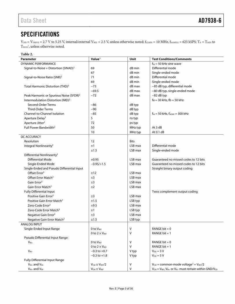
SPECIFICATIONS VDD = VDRIVE = 2.7 V to 5.25 V, internal/external VREF = 2.5 V, unless otherwise noted; fCLKIN = 10 MHz, fSAMPLE = 625 kSPS; TA = TMIN to TMAX
1, unless otherwise noted.
Table 2. Parameter Value1 Unit Test Conditions/Comments DYNAMIC PERFORMANCE fIN = 50 kHz sine wave
Signal-to-Noise + Distortion (SINAD)2 69 dB min Differential mode 67 dB min Single-ended mode
Signal-to-Noise Ratio (SNR)2 71 dB min Differential mode
69 dB min Single-ended mode Total Harmonic Distortion (THD)2 −73 dB max −85 dB typ, differential mode
−69.5 dB max −80 dB typ, single-ended mode Peak Harmonic or Spurious Noise (SFDR)2 −72 dB max −82 dB typ
Intermodulation Distortion (IMD)2 fa = 30 kHz, fb = 50 kHz
Second-Order Terms −86 dB typ Third-Order Terms −90 dB typ
Channel-to-Channel Isolation −85 dB typ fIN = 50 kHz, fNOISE = 300 kHz Aperture Delay2 5 ns typ
Aperture Jitter2 72 ps typ
Full Power Bandwidth2 50 MHz typ At 3 dB
10 MHz typ At 0.1 dB
DC ACCURACY Resolution 12 Bits Integral Nonlinearity2 ±1 LSB max Differential mode
±1.5 LSB max Single-ended mode Differential Nonlinearity2
Differential Mode ±0.95 LSB max Guaranteed no missed codes to 12 bits Single-Ended Mode −0.95/+1.5 LSB max Guaranteed no missed codes to 12 bits
Single-Ended and Pseudo Differential Input Straight binary output coding Offset Error2 ±12 LSB max
Offset Error Match2 ±3 LSB max
Gain Error2 ±3 LSB max
Gain Error Match2 ±2 LSB max
Fully Differential Input Twos complement output coding Positive Gain Error2 ±3 LSB max
Positive Gain Error Match2 ±1.5 LSB typ
Zero-Code Error2 ±9.5 LSB max
Zero-Code Error Match2 ±1 LSB typ
Negative Gain Error2 ±3 LSB max
Negative Gain Error Match2 ±1.5 LSB typ
ANALOG INPUT Single-Ended Input Range 0 to VREF V RANGE bit = 0
0 to 2 × VREF V RANGE bit = 1 Pseudo Differential Input Range:
VIN+ 0 to VREF V RANGE bit = 0 0 to 2 × VREF V RANGE bit = 1
VIN− −0.3 to +0.7 V typ VDD = 3 V −0.3 to +1.8 V typ VDD = 5 V
Fully Differential Input Range VIN+ and VIN− VCM ± VREF/2 V VCM = common-mode voltage3 = VREF/2 VIN+ and VIN− VCM ± VREF V VCM = VREF, VIN+ or VIN− must remain within GND/VDD

AD7938-6 Data Sheet
Rev. E | Page 4 of 30
Parameter Value1 Unit Test Conditions/Comments DC Leakage Current4 ±1 µA max Input Capacitance 45 pF typ When in track 10 pF typ When in hold
REFERENCE INPUT/OUTPUT VREF Input Voltage5 2.5 V ±1% for specified performance DC Leakage Current ±1 µA max VREFOUT Output Voltage 2.5 V ±0.2% max at 25°C VREFOUT Temperature Coefficient 25 ppm/°C max 5 ppm/°C typ VREF Noise 10 µV typ 0.1 Hz to 10 Hz bandwidth 130 µV typ 0.1 Hz to 1 MHz bandwidth VREF Output Impedance 10 Ω typ VREF Input Capacitance 15 pF typ When in track 25 pF typ When in hold
LOGIC INPUTS Input High Voltage, VINH 2.4 V min Input Low Voltage, VINL 0.8 V max Input Current, IIN ±5 µA max Typically 10 nA, VIN = 0 V or VDRIVE Input Capacitance, CIN
4 10 pF max
LOGIC OUTPUTS Output High Voltage, VOH 2.4 V min ISOURCE = 200 µA Output Low Voltage, VOL 0.4 V max ISINK = 200 µA Floating-State Leakage Current ±3 µA max Floating-State Output Capacitance4 10 pF max
Output Coding Straight (Natural) Binary CODING bit = 0 Twos Complement CODING bit = 1
CONVERSION RATE Conversion Time t2 + 13 tCLKIN ns Track-and-Hold Acquisition Time 125 ns max Full-scale step input 80 ns typ Sine wave input Throughput Rate 625 kSPS max
POWER REQUIREMENTS VDD 2.7/5.25 V min/max VDRIVE 2.7/5.25 V min/max IDD
6 Digital inputs = 0 V or VDRIVE Normal Mode (Static) 0.8 mA typ VDD = 2.7 V to 5.25 V, SCLK on or off Normal Mode (Operational) 1.5 mA max VDD = 4.75 V to 5.25 V
1.2 mA max VDD = 2.7 V to 3.6 V Autostandby Mode 0.3 mA typ fSAMPLE = 100 kSPS, VDD = 5 V 160 µA typ Static Full/Autoshutdown Mode (Static) 2 µA max SCLK on or off
Power Dissipation Normal Mode (Operational) 7.5 mW max VDD = 5 V 3.6 mW max VDD = 3 V Autostandby Mode (Static) 800 µW typ VDD = 5 V 480 µW typ VDD = 3 V Full/Autoshutdown Mode (Static) 10 µW max VDD = 5 V 6 µW max VDD = 3 V
1 Temperature range is −40°C to +85°C. 2 See the Terminology section. 3 For full common-mode range, see Figure 26 and Figure 27. 4 Sample tested during initial release to ensure compliance. 5 This device is operational with an external reference in the range of 0.1 V to VDD. See the Reference section for more information. 6 Measured with a midscale dc analog input.

Data Sheet AD7938-6
Rev. E | Page 5 of 30
TIMING SPECIFICATIONS VDD = VDRIVE = 2.7 V to 5.25 V, internal/external VREF = 2.5 V, unless otherwise noted; fCLKIN = 10MHz, fSAMPLE = 625 kSPS; TA = TMIN to TMAX, unless otherwise noted.
Table 3. Parameter1 Limit at TMIN, TMAX Unit Description fCLKIN
2 700 kHz min CLKIN frequency 10 MHz max tQUIET 30 ns min Minimum time between end of read and start of next conversion, that is, time from when
the data bus goes into three-state until the next falling edge of CONVST.
t1 10 ns min CONVST pulse width.
t2 15 ns min CONVST falling edge to CLKIN falling edge setup time.
t3 50 ns max CLKIN falling edge to BUSY rising edge. t4 0 ns min CS to WR setup time.
t5 0 ns min CS to WR hold time.
t6 10 ns min WR pulse width.
t7 10 ns min Data setup time before WR.
t8 10 ns min Data hold after WR.
t9 10 ns min New data valid before falling edge of BUSY. t10 0 ns min CS to RD setup time.
t11 0 ns min CS to RD hold time.
t12 30 ns min RD pulse width.
t133 30 ns max Data access time after RD.
t144 3 ns min Bus relinquish time after RD.
50 ns max Bus relinquish time after RD.
t15 0 ns min HBEN to RD setup time.
t16 0 ns min HBEN to RD hold time.
t17 10 ns min Minimum time between reads/writes. t18 0 ns min HBEN to WR setup time.
t19 10 ns min HBEN to WR hold time.
t20 40 ns max CLKIN falling edge to BUSY falling edge. t21 15.7 ns min CLKIN low pulse width. t22 7.8 ns min CLKIN high pulse width. 1 Sample tested during initial release to ensure compliance. All input signals are specified with tRISE = tFALL = 5 ns (10% to 90% of VDD) and timed from a voltage level of
1.6 V. All timing specifications given above are with a 25 pF load capacitance (see Figure 36, Figure 37, Figure 38, and Figure 39). 2 Minimum CLKIN for specified performance, with slower CLKIN frequencies performance specifications apply typically. 3 The time required for the output to cross 0.4 V or 2.4 V. 4 t14 is derived from the measured time taken by the data outputs to change 0.5 V. The measured number is then extrapolated back to remove the effects of charging or
discharging the 25 pF capacitor. This means that the time, t14, quoted in the timing characteristics is the true bus relinquish time of the part and is independent of the bus loading.
AD7938-6 Data Sheet
Rev. E | Page 6 of 30
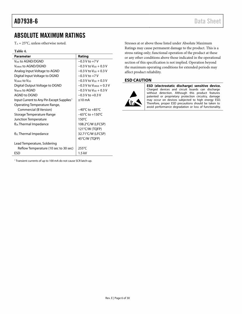
ABSOLUTE MAXIMUM RATINGS TA = 25°C, unless otherwise noted.
Table 4. Parameter Rating VDD to AGND/DGND −0.3 V to +7 V VDRIVE to AGND/DGND −0.3 V to VDD + 0.3 V Analog Input Voltage to AGND −0.3 V to VDD + 0.3 V Digital Input Voltage to DGND −0.3 V to +7 V VDRIVE to VDD −0.3 V to VDD + 0.3 V Digital Output Voltage to DGND −0.3 V to VDRIVE + 0.3 V VREFIN to AGND −0.3 V to VDD + 0.3 V AGND to DGND −0.3 V to +0.3 V Input Current to Any Pin Except Supplies1 ±10 mA Operating Temperature Range,
Commercial (B Version) −40°C to +85°C Storage Temperature Range −65°C to +150°C Junction Temperature 150°C θJA Thermal Impedance 108.2°C/W (LFCSP) 121°C/W (TQFP) θJC Thermal Impedance 32.71°C/W (LFCSP) 45°C/W (TQFP) Lead Temperature, Soldering
Reflow Temperature (10 sec to 30 sec) 255°C ESD 1.5 kV 1 Transient currents of up to 100 mA do not cause SCR latch-up.
Stresses at or above those listed under Absolute Maximum Ratings may cause permanent damage to the product. This is a stress rating only; functional operation of the product at these or any other conditions above those indicated in the operational section of this specification is not implied. Operation beyond the maximum operating conditions for extended periods may affect product reliability.
ESD CAUTION
Data Sheet AD7938-6
Rev. E | Page 7 of 30
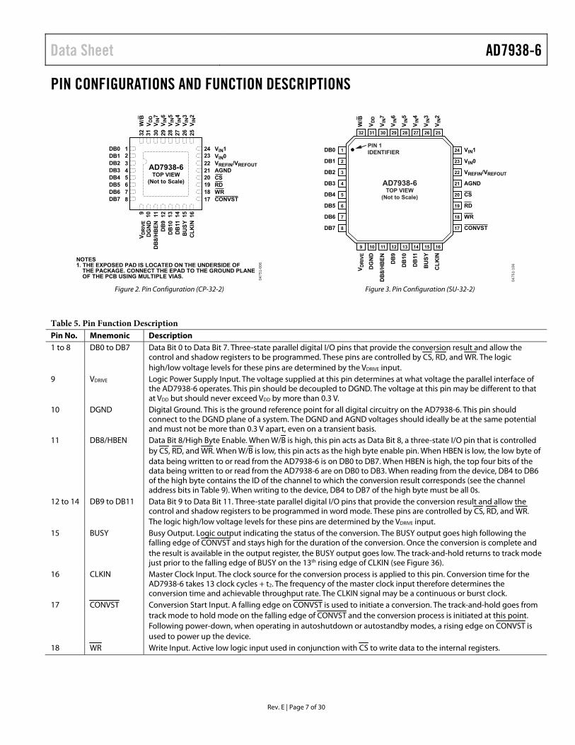
PIN CONFIGURATIONS AND FUNCTION DESCRIPTIONS
DB0DB1DB2DB3DB4DB5DB6DB7
NOTES1. THE EXPOSED PAD IS LOCATED ON THE UNDERSIDE OF
THE PACKAGE. CONNECT THE EPAD TO THE GROUND PLANEOF THE PCB USING MULTIPLE VIAS.
24 VIN123 VIN022 VREFIN/VREFOUT21 AGND20 CS19 RD18 WR17 CONVST
12345678
9 10 11 12 13 14 15 16
VD
RIV
ED
GN
DD
B8/
HB
EN
DB
9D
B10
DB
11B
US
YC
LK
IN
32 31 30 29 28 27 26 25
W/B
VD
DV
IN7
VIN
6V
IN5
VIN
4V
IN3
VIN
2
AD7938-6TOP VIEW
(Not to Scale)
0475
1-00
6
0475
1-10
6
DB0 1
VD
RIV
E
9
DG
ND
10
DB
8/H
BE
N
11
DB
9
12
DB
10
13
DB
11
14
BU
SY
15
CL
KIN
16
W/B
32
VD
D
31
VIN
7
30
VIN
6
29
VIN
5
28
VIN
4
27
VIN
3
26
VIN
2
25
DB1 2
DB2 3
DB3 4
DB4 5
DB5 6
DB6 7
DB7 8
VIN124
VIN023
VREFIN/VREFOUT22
AGND21
20
19
WR18
CONVST17
AD7938-6TOP VIEW
(Not to Scale)
RD
CS
PIN 1IDENTIFIER
Figure 2. Pin Configuration (CP-32-2) Figure 3. Pin Configuration (SU-32-2)
Table 5. Pin Function Description Pin No. Mnemonic Description 1 to 8 DB0 to DB7 Data Bit 0 to Data Bit 7. Three-state parallel digital I/O pins that provide the conversion result and allow the
control and shadow registers to be programmed. These pins are controlled by CS, RD, and WR. The logic high/low voltage levels for these pins are determined by the VDRIVE input.
9 VDRIVE Logic Power Supply Input. The voltage supplied at this pin determines at what voltage the parallel interface of the AD7938-6 operates. This pin should be decoupled to DGND. The voltage at this pin may be different to that at VDD but should never exceed VDD by more than 0.3 V.
10 DGND Digital Ground. This is the ground reference point for all digital circuitry on the AD7938-6. This pin should connect to the DGND plane of a system. The DGND and AGND voltages should ideally be at the same potential and must not be more than 0.3 V apart, even on a transient basis.
11 DB8/HBEN Data Bit 8/High Byte Enable. When W/B is high, this pin acts as Data Bit 8, a three-state I/O pin that is controlled by CS, RD, and WR. When W/B is low, this pin acts as the high byte enable pin. When HBEN is low, the low byte of data being written to or read from the AD7938-6 is on DB0 to DB7. When HBEN is high, the top four bits of the data being written to or read from the AD7938-6 are on DB0 to DB3. When reading from the device, DB4 to DB6 of the high byte contains the ID of the channel to which the conversion result corresponds (see the channel address bits in Table 9). When writing to the device, DB4 to DB7 of the high byte must be all 0s.
12 to 14 DB9 to DB11 Data Bit 9 to Data Bit 11. Three-state parallel digital I/O pins that provide the conversion result and allow the control and shadow registers to be programmed in word mode. These pins are controlled by CS, RD, and WR. The logic high/low voltage levels for these pins are determined by the VDRIVE input.
15 BUSY Busy Output. Logic output indicating the status of the conversion. The BUSY output goes high following the falling edge of CONVST and stays high for the duration of the conversion. Once the conversion is complete and the result is available in the output register, the BUSY output goes low. The track-and-hold returns to track mode just prior to the falling edge of BUSY on the 13th rising edge of CLKIN (see Figure 36).
16 CLKIN Master Clock Input. The clock source for the conversion process is applied to this pin. Conversion time for the AD7938-6 takes 13 clock cycles + t2. The frequency of the master clock input therefore determines the conversion time and achievable throughput rate. The CLKIN signal may be a continuous or burst clock.
17 CONVST Conversion Start Input. A falling edge on CONVST is used to initiate a conversion. The track-and-hold goes from track mode to hold mode on the falling edge of CONVST and the conversion process is initiated at this point. Following power-down, when operating in autoshutdown or autostandby modes, a rising edge on CONVST is used to power up the device.
18 WR Write Input. Active low logic input used in conjunction with CS to write data to the internal registers.
AD7938-6 Data Sheet
Rev. E | Page 8 of 30
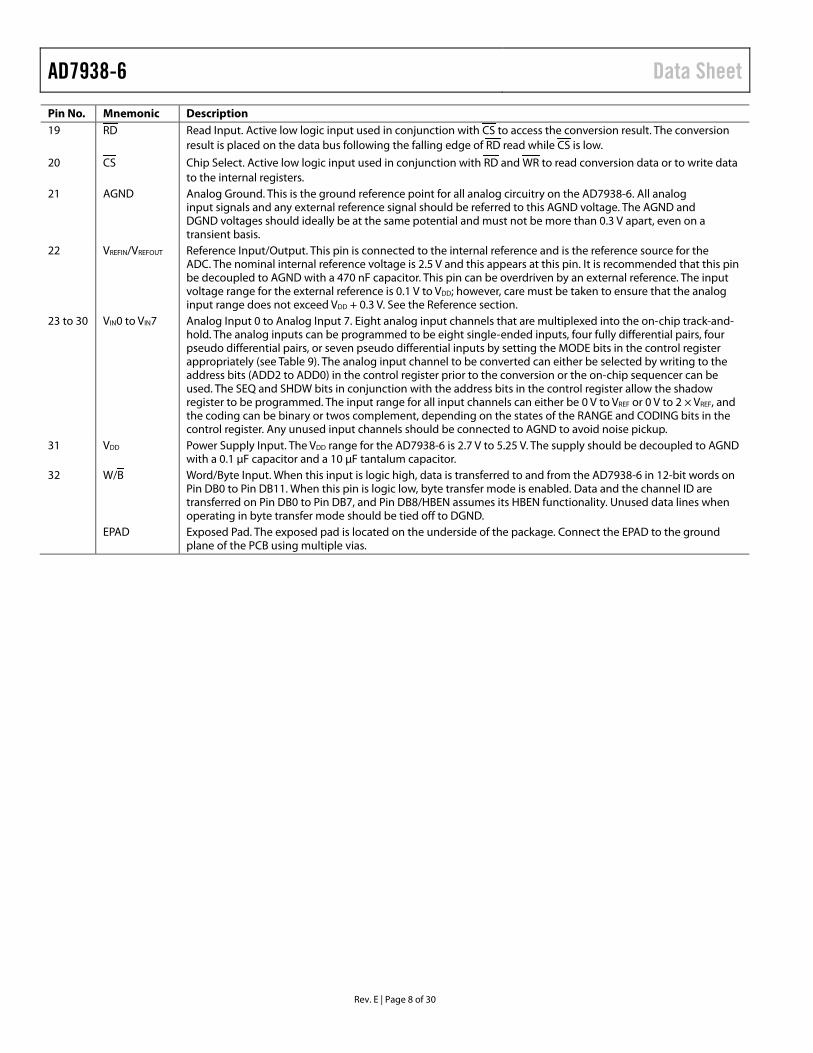
Pin No. Mnemonic Description 19 RD Read Input. Active low logic input used in conjunction with CS to access the conversion result. The conversion
result is placed on the data bus following the falling edge of RD read while CS is low.
20 CS Chip Select. Active low logic input used in conjunction with RD and WR to read conversion data or to write data to the internal registers.
21 AGND Analog Ground. This is the ground reference point for all analog circuitry on the AD7938-6. All analog input signals and any external reference signal should be referred to this AGND voltage. The AGND and DGND voltages should ideally be at the same potential and must not be more than 0.3 V apart, even on a transient basis.
22 VREFIN/VREFOUT Reference Input/Output. This pin is connected to the internal reference and is the reference source for the ADC. The nominal internal reference voltage is 2.5 V and this appears at this pin. It is recommended that this pin be decoupled to AGND with a 470 nF capacitor. This pin can be overdriven by an external reference. The input voltage range for the external reference is 0.1 V to VDD; however, care must be taken to ensure that the analog input range does not exceed VDD + 0.3 V. See the Reference section.
23 to 30 VIN0 to VIN7 Analog Input 0 to Analog Input 7. Eight analog input channels that are multiplexed into the on-chip track-and-hold. The analog inputs can be programmed to be eight single-ended inputs, four fully differential pairs, four pseudo differential pairs, or seven pseudo differential inputs by setting the MODE bits in the control register appropriately (see Table 9). The analog input channel to be converted can either be selected by writing to the address bits (ADD2 to ADD0) in the control register prior to the conversion or the on-chip sequencer can be used. The SEQ and SHDW bits in conjunction with the address bits in the control register allow the shadow register to be programmed. The input range for all input channels can either be 0 V to VREF or 0 V to 2 × VREF, and the coding can be binary or twos complement, depending on the states of the RANGE and CODING bits in the control register. Any unused input channels should be connected to AGND to avoid noise pickup.
31 VDD Power Supply Input. The VDD range for the AD7938-6 is 2.7 V to 5.25 V. The supply should be decoupled to AGND with a 0.1 µF capacitor and a 10 µF tantalum capacitor.
32 W/B Word/Byte Input. When this input is logic high, data is transferred to and from the AD7938-6 in 12-bit words on Pin DB0 to Pin DB11. When this pin is logic low, byte transfer mode is enabled. Data and the channel ID are transferred on Pin DB0 to Pin DB7, and Pin DB8/HBEN assumes its HBEN functionality. Unused data lines when operating in byte transfer mode should be tied off to DGND.
EPAD Exposed Pad. The exposed pad is located on the underside of the package. Connect the EPAD to the ground plane of the PCB using multiple vias.
Data Sheet AD7938-6
Rev. E | Page 9 of 30
TYPICAL PERFORMANCE CHARACTERISTICS TA = 25°C, unless otherwise noted.
SUPPLY RIPPLE FREQUENCY (kHz)
PS
RR
(d
B)
–60
–70
–80
–90
–110
–100
–12010 210 610410 810 1010
0475
1-00
7
100mV p-p SINE WAVE ON VDD AND/OR VDRIVENO DECOUPLINGDIFFERENTIAL/SINGLE-ENDED MODE
INT REF
EXT REF
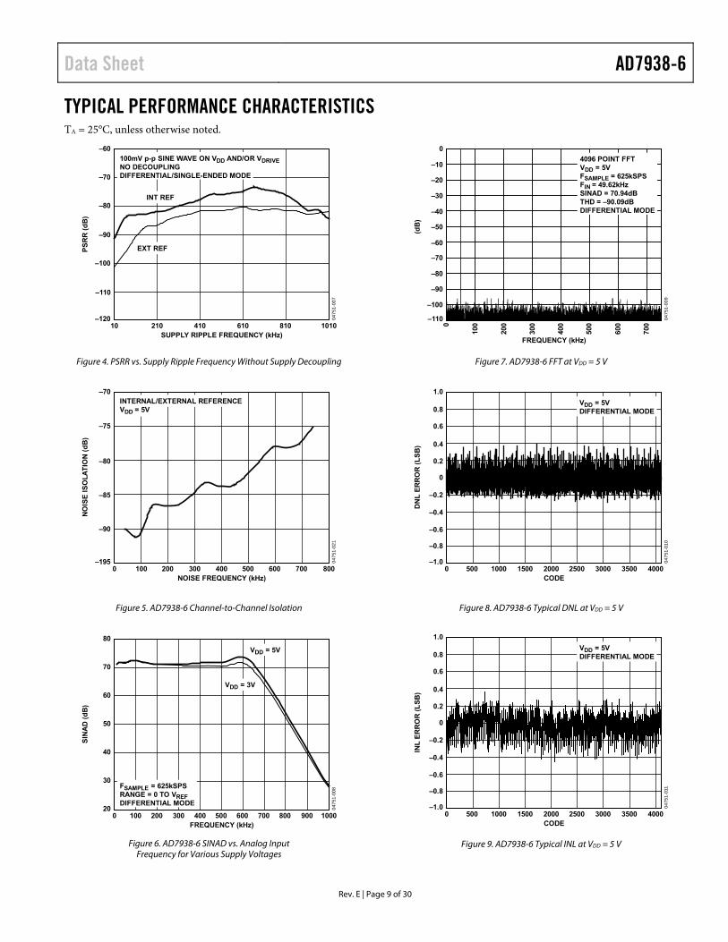
Figure 4. PSRR vs. Supply Ripple Frequency Without Supply Decoupling
NOISE FREQUENCY (kHz)
NO
ISE
IS
OL
AT
ION
(d
B)
–70
–75
–90
–85
–80
–1950 100 400200 300 600500 800700
0475
1-02
1
INTERNAL/EXTERNAL REFERENCEVDD = 5V
Figure 5. AD7938-6 Channel-to-Channel Isolation
FREQUENCY (kHz)
SIN
AD
(d
B)
80
70
60
30
40
50
200 100 400200 300 600500 1000700 800 900
0475
1-00
8FSAMPLE = 625kSPSRANGE = 0 TO VREFDIFFERENTIAL MODE
VDD = 5V
VDD = 3V
Figure 6. AD7938-6 SINAD vs. Analog Input Frequency for Various Supply Voltages
FREQUENCY (kHz)
0
–10
–20
–50
–40
–30
–90
–100
–80
–70
–60
–110
0
100
200
300
400
500
600
700
0475
1-00
9
4096 POINT FFTVDD = 5VFSAMPLE = 625kSPSFIN = 49.62kHzSINAD = 70.94dBTHD = –90.09dBDIFFERENTIAL MODE
(dB
)
Figure 7. AD7938-6 FFT at VDD = 5 V
CODE
DN
L E
RR
OR
(L
SB
)
1.0
0.8
0.6
0.4
0.2
–0.2
0
–0.8
–0.6
–0.4
–1.00 500 20001000 1500 30002500 40003500
0475
1-01
0
VDD = 5VDIFFERENTIAL MODE
Figure 8. AD7938-6 Typical DNL at VDD = 5 V
CODE
INL
ER
RO
R (
LS
B)
1.0
0.8
0.6
0.4
0.2
–0.2
0
–0.8
–0.6
–0.4
–1.00 500 20001000 1500 30002500 40003500
0475
1-01
1
VDD = 5VDIFFERENTIAL MODE
Figure 9. AD7938-6 Typical INL at VDD = 5 V

AD7938-6 Data Sheet
Rev. E | Page 10 of 30
VREF (V)
DN
L (
LS
B)
6
5
4
3
1
2
0
–10.25 0.50 1.250.75 1.00 2.001.751.50 2.752.502.25
0475
1-01
2
SINGLE-ENDED MODE
POSITIVE DNL
NEGATIVE DNL
Figure 10. AD7938-6 DNL vs. VREF for VDD = 3 V
VREF (V)
EF
FE
CT
IVE
NU
MB
ER
OF
BIT
S
12
11
10
8
9
7
60 0.5 1.51.0 2.52.0 4.03.53.0
0475
1-01
3
VDD = 5VDIFFERENTIAL MODE
VDD = 5VSINGLE-ENDED MODE
VDD = 3VSINGLE-ENDED MODE
VDD = 3VDIFFERENTIAL MODE
Figure 11. AD7938-6 ENOB vs. VREF
VREF (V)
OF
FS
ET
(L
SB
)
0
–0.5
–1.5
–1.0
–3.5
–3.0
–2.5
–2.0
–4.0
–4.5
–5.00 0.5 1.51.0 2.52.0 3.53.0
0475
1-01
4
SINGLE-ENDED MODE
VDD = 5V
VDD = 3V
Figure 12. AD7938-6 Offset vs. VREF
CODE
??
?
10000
9000
7000
8000
3000
4000
5000
6000
2000
1000
02046 2047 2048 2049 2050
0475
1-01
5
DIFFERENTIAL MODE
3 CODES
INTERNALREF
9997CODES
Figure 13. AD7938-6 Histogram of Codes for 10,000 Samples at VDD = 5 V with Internal Reference
RIPPLE FREQUENCY (kHz)
CM
RR
(d
B)
60
70
80
100
90
110
120
0 200 400 800600 12001000
0475
1-01
7
DIFFERENTIAL MODE
Figure 14. CMRR vs. Input Frequency with VDD = 5 V and 3 V

Data Sheet AD7938-6
Rev. E | Page 11 of 30
TERMINOLOGY Integral Nonlinearity (INL) This is the maximum deviation from a straight line passing through the endpoints of the ADC transfer function. The endpoints of the transfer function are zero scale, 1 LSB below the first code transition, and full scale, 1 LSB above the last code transition.
Differential Nonlinearity This is the difference between the measured and the ideal 1 LSB change between any two adjacent codes in the ADC.
Offset Error This is the deviation of the first code transition (00…000) to (00…001) from the ideal (that is, AGND + 1 LSB).
Offset Error Match
This is the difference in offset error between any two channels.
Gain Error This is the deviation of the last code transition (111…110) to (111…111) from the ideal (that is, VREF – 1 LSB) after the offset error has been adjusted out.
Gain Error Match This is the difference in gain error between any two channels.
Zero-Code Error This applies when using the twos complement output coding option, in particular to the 2 × VREF input range with −VREF to +VREF biased about the VREFIN point. It is the deviation of the midscale transition (all 0s to all 1s) from the ideal VIN voltage, (that is, VREF).
Zero-Code Error Match This is the difference in zero-code error between any two channels.
Positive Gain Error This applies when using the twos complement output coding option, in particular to the 2 × VREF input range with −VREF to +VREF biased about the VREFIN point. It is the deviation of the last code transition (011…110) to (011…111) from the ideal (that is, +VREF − 1 LSB) after the zero-code error has been adjusted out.
Positive Gain Error Match This is the difference in positive gain error between any two channels.
Negative Gain Error This applies when using the twos complement output coding option, in particular to the 2 × VREF input range with −VREF to +VREF biased about the VREF point. It is the deviation of the first code transition (100…000) to (100…001) from the ideal (that is, −VREF + 1 LSB) after the zero-code error has been adjusted out.
Negative Gain Error Match This is the difference in negative gain error between any two channels.
Channel-to-Channel Isolation Channel-to-channel isolation is a measure of the level of crosstalk between channels. It is measured by applying a full-scale sine wave signal to all seven nonselected input channels and applying a 50 kHz signal to the selected channel. The channel-to-channel isolation is defined as the ratio of the power of the 50 kHz signal on the selected channel to the power of the noise signal on the unselected channels that appears in the FFT of this channel. The noise frequency on the unselected channels varies from 40 kHz to 740 kHz. The noise amplitude is at 2 × VREF, while the signal amplitude is at 1 × VREF. See Figure 5.
Power Supply Rejection Ratio (PSRR) PSRR is defined as the ratio of the power in the ADC output at full-scale frequency, f, to the power of a 100 mV p-p sine wave applied to the ADC VDD supply of frequency, fS. The frequency of the noise varies from 1 kHz to 1 MHz.
PSRR (dB) = 10 log(Pf/PfS)
where:
Pf is the power at frequency f in the ADC output. PfS is the power at frequency fS in the ADC output.
Common-Mode Rejection Ratio (CMRR) CMRR is defined as the ratio of the power in the ADC output at full-scale frequency, f, to the power of a 100 mV p-p sine wave applied to the common-mode voltage of VIN+ and VIN− of frequency, fS.
CMRR (dB) = 10 log(Pf/PfS)
where:
Pf is the power at frequency f in the ADC output. PfS is the power at frequency fS in the ADC output.
AD7938-6 Data Sheet
Rev. E | Page 12 of 30
Track-and-Hold Acquisition Time The track-and-hold amplifier returns to track mode at the end of conversion. The track-and-hold acquisition time is the time required for the output of the track-and-hold amplifier to reach its final value, within ±1/2 LSB, after the end of conversion.
Signal to Noise and Distortion Ratio (SINAD) This is the measured ratio of signal-to-noise and distortion at the output of the ADC. The signal is the rms amplitude of the fundamental. Noise is the sum of all nonfundamental signals up to half the sampling frequency (fSAMPLE/2), excluding dc. The ratio is dependent on the number of quantization levels in the digitization process; the more levels, the smaller the quantization noise.
The theoretical SINAD ratio for an ideal N-bit converter with a sine wave input is given by
SINAD = (6.02 N + 1.76) dB
Thus, for a 12-bit converter, SINAD is 74 dB.
Total Harmonic Distortion (THD) THD is the ratio of the rms sum of harmonics to the fundamental. For the AD7938-6, it is defined as:
( )
++++−=
1
65432
VVVVVV
THD22222
log20dB
where:
V1 is the rms amplitude of the fundamental. V2, V3, V4, V5, and V6 are the rms amplitudes of the second through the sixth harmonics.
Peak Harmonic or Spurious Noise Peak harmonic or spurious noise is defined as the ratio of the rms value of the next largest component in the ADC output spectrum (up to fSAMPLE/2 and excluding dc) to the rms value of the fundamental. Normally, the value of this specification is determined by the largest harmonic in the spectrum, but for ADCs where the harmonics are buried in the noise floor, it is a noise peak.
Intermodulation Distortion With inputs consisting of sine waves at two frequencies, fa and fb, any active device with nonlinearities creates distortion products at sum and difference frequencies of mfa ± nfb where m, n = 0, 1, 2, 3, and so on. Intermodulation distortion terms are those for which neither m nor n are equal to 0. For example, the second-order terms include (fa + fb) and (fa − fb), and the third-order terms include (2fa + fb), (2fa − fb), (fa + 2fb) and (fa − 2fb).
The AD7938-6 is tested using the CCIF standard where two input frequencies near the top end of the input bandwidth are used. In this case, the second-order terms are usually distanced in frequency from the original sine waves while the third-order terms are usually at a frequency close to the input frequencies. As a result, the second-order and third-order terms are specified separately. The intermodulation distortion is calculated per the THD specification, as the ratio of the rms sum of the individual distortion products to the rms amplitude of the sum of the fundamentals, expressed in dB.
Data Sheet AD7938-6
Rev. E | Page 13 of 30
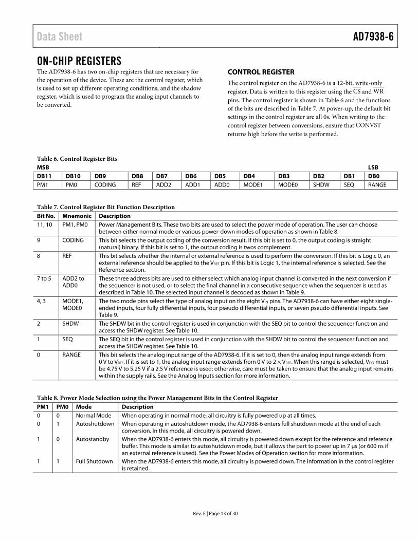
ON-CHIP REGISTERS The AD7938-6 has two on-chip registers that are necessary for the operation of the device. These are the control register, which is used to set up different operating conditions, and the shadow register, which is used to program the analog input channels to be converted.
CONTROL REGISTER The control register on the AD7938-6 is a 12-bit, write-only register. Data is written to this register using the CS and WR pins. The control register is shown in Table 6 and the functions of the bits are described in Table 7. At power-up, the default bit settings in the control register are all 0s. When writing to the control register between conversions, ensure that CONVST returns high before the write is performed.
Table 6. Control Register Bits MSB LSB DB11 DB10 DB9 DB8 DB7 DB6 DB5 DB4 DB3 DB2 DB1 DB0 PM1 PM0 CODING REF ADD2 ADD1 ADD0 MODE1 MODE0 SHDW SEQ RANGE
Table 7. Control Register Bit Function Description Bit No. Mnemonic Description 11, 10 PM1, PM0 Power Management Bits. These two bits are used to select the power mode of operation. The user can choose
between either normal mode or various power-down modes of operation as shown in Table 8. 9 CODING This bit selects the output coding of the conversion result. If this bit is set to 0, the output coding is straight
(natural) binary. If this bit is set to 1, the output coding is twos complement. 8 REF This bit selects whether the internal or external reference is used to perform the conversion. If this bit is Logic 0, an
external reference should be applied to the VREF pin. If this bit is Logic 1, the internal reference is selected. See the Reference section.
7 to 5 ADD2 to ADD0
These three address bits are used to either select which analog input channel is converted in the next conversion if the sequencer is not used, or to select the final channel in a consecutive sequence when the sequencer is used as described in Table 10. The selected input channel is decoded as shown in Table 9.
4, 3 MODE1, MODE0
The two mode pins select the type of analog input on the eight VIN pins. The AD7938-6 can have either eight single-ended inputs, four fully differential inputs, four pseudo differential inputs, or seven pseudo differential inputs. See Table 9.
2 SHDW The SHDW bit in the control register is used in conjunction with the SEQ bit to control the sequencer function and access the SHDW register. See Table 10.
1 SEQ The SEQ bit in the control register is used in conjunction with the SHDW bit to control the sequencer function and access the SHDW register. See Table 10.
0 RANGE This bit selects the analog input range of the AD7938-6. If it is set to 0, then the analog input range extends from 0 V to VREF. If it is set to 1, the analog input range extends from 0 V to 2 × VREF. When this range is selected, VDD must be 4.75 V to 5.25 V if a 2.5 V reference is used; otherwise, care must be taken to ensure that the analog input remains within the supply rails. See the Analog Inputs section for more information.
Table 8. Power Mode Selection using the Power Management Bits in the Control Register PM1 PM0 Mode Description 0 0 Normal Mode When operating in normal mode, all circuitry is fully powered up at all times. 0 1 Autoshutdown When operating in autoshutdown mode, the AD7938-6 enters full shutdown mode at the end of each
conversion. In this mode, all circuitry is powered down. 1 0 Autostandby When the AD7938-6 enters this mode, all circuitry is powered down except for the reference and reference
buffer. This mode is similar to autoshutdown mode, but it allows the part to power up in 7 µs (or 600 ns if an external reference is used). See the Power Modes of Operation section for more information.
1 1 Full Shutdown When the AD7938-6 enters this mode, all circuitry is powered down. The information in the control register is retained.

AD7938-6 Data Sheet
Rev. E | Page 14 of 30
Table 9. Analog Input Type Selection
Channel Address
MODE0 = 0, MODE1 = 0 MODE0 = 0, MODE1 = 1 MODE0 = 1, MODE1 = 0 MODE0 = 1, MODE1 = 1
Eight Single-Ended Input Channels
Four Fully Differential Input Channels
Four Pseudo Differential Input Channels (Pseudo Mode 1)
Seven Pseudo Differential Input Channels (Pseudo Mode 2)
ADD2 ADD1 ADD0 VIN+ VIN− VIN+ VIN− VIN+ VIN− VIN+ VIN−
0 0 0 VIN0 AGND VIN0 VIN1 VIN0 VIN1 VIN0 VIN7 0 0 1 VIN1 AGND VIN1 VIN0 VIN1 VIN0 VIN1 VIN7 0 1 0 VIN2 AGND VIN2 VIN3 VIN2 VIN3 VIN2 VIN7 0 1 1 VIN3 AGND VIN3 VIN2 VIN3 VIN2 VIN3 VIN7 1 0 0 VIN4 AGND VIN4 VIN5 VIN4 VIN5 VIN4 VIN7 1 0 1 VIN5 AGND VIN5 VIN4 VIN5 VIN4 VIN5 VIN7 1 1 0 VIN6 AGND VIN6 VIN7 VIN6 VIN7 VIN6 VIN7 1 1 1 VIN7 AGND VIN7 VIN6 VIN7 VIN6 Not Allowed Not Allowed
SEQUENCER OPERATION The configuration of the SEQ and SHDW bits in the control register allows the user to select a particular mode of operation of the sequencer function. Table 10 outlines the four modes of operation of the sequencer.
Writing to the Control Register to Program the Sequencer
The AD7938-6 needs 13 full CLKIN periods to perform a conversion. If the ADC does not receive the full 13 CLKIN periods, the conversion aborts. If a conversion is aborted after applying 12.5 CLKIN periods to the ADC, ensure that a rising edge of CONVST or a falling edge of CLKIN is applied to the part before writing to the control register to program the sequencer. If these conditions are not met, the sequencer will not be in the correct state to handle being reprogrammed for another sequence of conversions and the performance of the converter is not guaranteed.
SHADOW REGISTER The shadow register on the AD7938-6 is an 8-bit, write-only register. Data is loaded from DB0 to DB7 on the rising edge of WR. The eight LSBs load into the shadow register. The information is written into the shadow register provided that
the SEQ and SHDW bits in the control register were set to 0 and 1, respectively, in the previous write to the control register. Each bit represents an analog input from Channel 0 through Channel 7. A sequence of channels can be selected through which the AD7938-6 cycles with each consecutive conversion after the write to the shadow register.
To select a sequence of channels to be converted, if operating in single-ended mode or Pseudo Mode 2, the associated channel bit in the shadow register must be set for each required analog input. When operating in fully differential mode or Pseudo Mode 1, the associated pair of channel bits must be set for each pair of analog inputs required in the sequence.
With each consecutive CONVST pulse after the sequencer has been set up, the AD7938-6 progresses through the selected channels in ascending order, beginning with the lowest channel. This continues until a write operation occurs with the SEQ and SHDW bits configured in any way except 1, 0 (see Table 10). When a sequence is set up in differential mode or Pseudo Mode 1, the ADC does not convert on the inverse pairs (that is, VIN1, VIN0). The bit functions of the shadow register are outlined in Table 11. See the Analog Input Selection section for further information on using the sequencer.
Data Sheet AD7938-6
Rev. E | Page 15 of 30
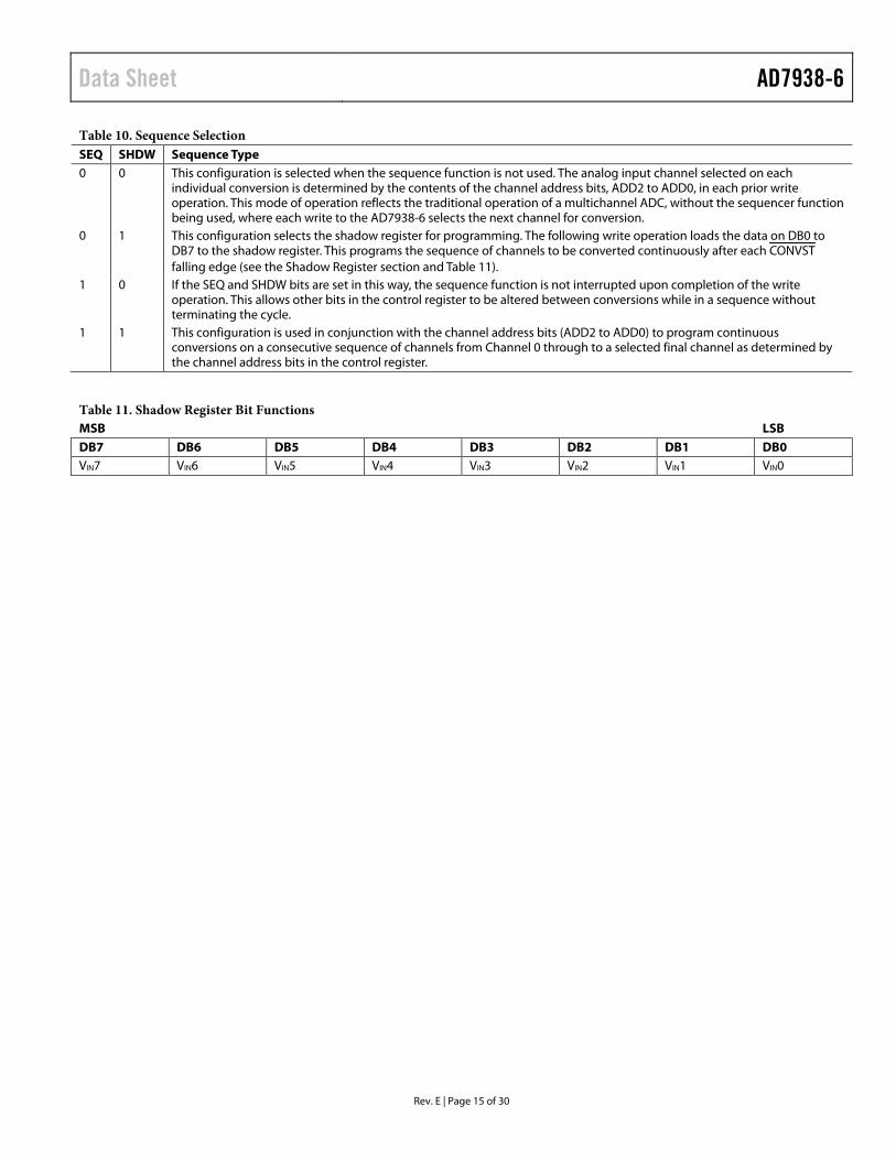
Table 10. Sequence Selection SEQ SHDW Sequence Type 0 0 This configuration is selected when the sequence function is not used. The analog input channel selected on each
individual conversion is determined by the contents of the channel address bits, ADD2 to ADD0, in each prior write operation. This mode of operation reflects the traditional operation of a multichannel ADC, without the sequencer function being used, where each write to the AD7938-6 selects the next channel for conversion.
0 1 This configuration selects the shadow register for programming. The following write operation loads the data on DB0 to DB7 to the shadow register. This programs the sequence of channels to be converted continuously after each CONVST falling edge (see the Shadow Register section and Table 11).
1 0 If the SEQ and SHDW bits are set in this way, the sequence function is not interrupted upon completion of the write operation. This allows other bits in the control register to be altered between conversions while in a sequence without terminating the cycle.
1 1 This configuration is used in conjunction with the channel address bits (ADD2 to ADD0) to program continuous conversions on a consecutive sequence of channels from Channel 0 through to a selected final channel as determined by the channel address bits in the control register.
Table 11. Shadow Register Bit Functions MSB LSB DB7 DB6 DB5 DB4 DB3 DB2 DB1 DB0 VIN7 VIN6 VIN5 VIN4 VIN3 VIN2 VIN1 VIN0

AD7938-6 Data Sheet
Rev. E | Page 16 of 30
CIRCUIT INFORMATION The AD7938-6 is a fast, 8-channel, 12-bit, single-supply, successive approximation analog-to-digital converter. The part can operate from a 2.7 V to 5.25 V power supply and features throughput rates up to 625 kSPS.
The AD7938-6 provides the user with an on-chip track-and-hold, an accurate internal reference, an analog-to-digital converter, and a parallel interface housed in a 32-lead LFCSP or TQFP package.
The AD7938-6 has eight analog input channels that can be configured to be eight single-ended inputs, four fully differential pairs, four pseudo differential pairs, or seven pseudo differential inputs with respect to one common input. There is an on-chip user-programmable channel sequencer that allows the user to select a sequence of channels through which the ADC can progress and cycle with each consecutive falling edge of CONVST.
The analog input range for the AD7938-6 is 0 V to VREF or 0 V to 2 × VREF depending on the status of the RANGE bit in the control register. The output coding of the ADC can be either straight binary or twos complement, depending on the status of the CODING bit in the control register.
The AD7938-6 provides flexible power management options to allow the user to achieve the best power performance for a given throughput rate. These options are selected by programming the power management bits, PM1 and PM0, in the control register.
CONVERTER OPERATION The AD7938-6 is a successive approximation ADC based around two capacitive digital-to-analog converters. Figure 15 and Figure 16 show simplified schematics of the ADC in acquisition and conversion phase, respectively. The ADC comprises control logic, an SAR, and two capacitive digital-to-analog converters. Both figures show the operation of the ADC in differential/pseudo differential mode. Single-ended mode operation is similar but VIN− is internally tied to AGND. In acquisition phase, SW3 is closed, SW1 and SW2 are in Position A, the comparator is held in a balanced condition and the sampling capacitor arrays acquire the differential signal on the input.
0475
1-02
3
VIN+
VIN–
A
B
SW1
SW3
COMPARATOR
CONTROLLOGIC
CAPACITIVEDAC
CAPACITIVEDAC
CS
CSVREF
SW2
B
A
Figure 15. ADC Acquisition Phase
When the ADC starts a conversion (see Figure 16), SW3 opens and SW1 and SW2 move to Position B, causing the comparator to become unbalanced. Both inputs are disconnected once the conversion begins. The control logic and the charge redistribution DACs are used to add and subtract fixed amounts of charge from the sampling capacitor arrays to bring the comparator back into a balanced condition. When the comparator is rebalanced, the conversion is complete. The control logic generates the output code of the ADC. The output impedances of the sources driving the VIN+ and the VIN− pins must match; otherwise, the two inputs have different settling times, resulting in errors.
0475
1-02
4
VIN+
VIN–
A
B
SW1
SW3
COMPARATOR
CONTROLLOGIC
CAPACITIVEDAC
CAPACITIVEDAC
CS
CSVREF
SW2
B
A
Figure 16. ADC Conversion Phase
ADC TRANSFER FUNCTION The output coding for the AD7938-6 is either straight binary or twos complement, depending on the status of the CODING bit in the control register. The designed code transitions occur at successive LSB values (that is, 1 LSB, 2 LSBs, and so on) and the LSB size is VREF/4096. The ideal transfer characteristics of the AD7938-6 for both straight binary and twos complement output coding are shown in Figure 17 and Figure 18, respectively.
0475
1-02
5
000...000
111...111
1 LSB = VREF/4096
1 LSB +VREF – 1 LSB
ANALOG INPUT
AD
C C
OD
E
0V
NOTE: VREF IS EITHER VREF OR 2 × VREF
000...001
000...010
111...110
111...000
011...111
Figure 17. AD7938-6 Ideal Transfer Characteristic
with Straight Binary Output Coding
Data Sheet AD7938-6
Rev. E | Page 17 of 30
0475
1-02
6
100...000
011...111
1 LSB = 2 × VREF/4096
–VREF + 1 LSB VREF +VREF – 1 LSB
AD
C C
OD
E
100...001
100...010
011...110
000...001
000...000
111...111
Figure 18. AD7938-6 Ideal Transfer Characteristic
with Twos Complement Output Coding and 2 × VREF Range
TYPICAL CONNECTION DIAGRAM Figure 19 shows a typical connection diagram for the AD7938-6. The AGND and DGND pins are connected together at the device for good noise suppression. The VREFIN/VREFOUT pin is decoupled to AGND with a 0.47 μF capacitor to avoid noise pickup if the internal reference is used. Alternatively, VREFIN/VREFOUT can be connected to an external reference source. In this case, the reference pin should be decoupled with a 0.1 μF capacitor. In both cases, the analog input range can either be 0 V to VREF (RANGE bit = 0) or 0 V to 2 × VREF (RANGE bit = 1). The analog input configuration can be either eight single-ended inputs, four differential pairs, four pseudo differential pairs, or seven pseudo differential inputs (see Table 9). The VDD pin is connected to either a 3 V or 5 V supply. The voltage applied to the VDRIVE input controls the voltage of the digital interface and here, it is connected to the same 3 V supply of the microprocessor to allow a 3 V logic interface (see the Digital Inputs section).
0475
1-02
7
0.1µF 10µF
3V/5VSUPPLY
3VSUPPLY
MIC
RO
CO
NT
RO
LL
ER
/M
ICR
OP
RO
CE
SS
OR
AD7938-6
0.1µF
0.1µF EXTERNAL VREF0.47µF INTERNAL VREF
0 TO VREF/0 TO 2 × VREF
AGND
DGND
W/B
CLKIN
CS
VDRIVE
VIN0
VDD
VREFIN/VREFOUT
VIN7
10µF
2.5VVREF
RD
CONVST
WR
BUSY
DB0
DB11/DB9
Figure 19. Typical Connection Diagram
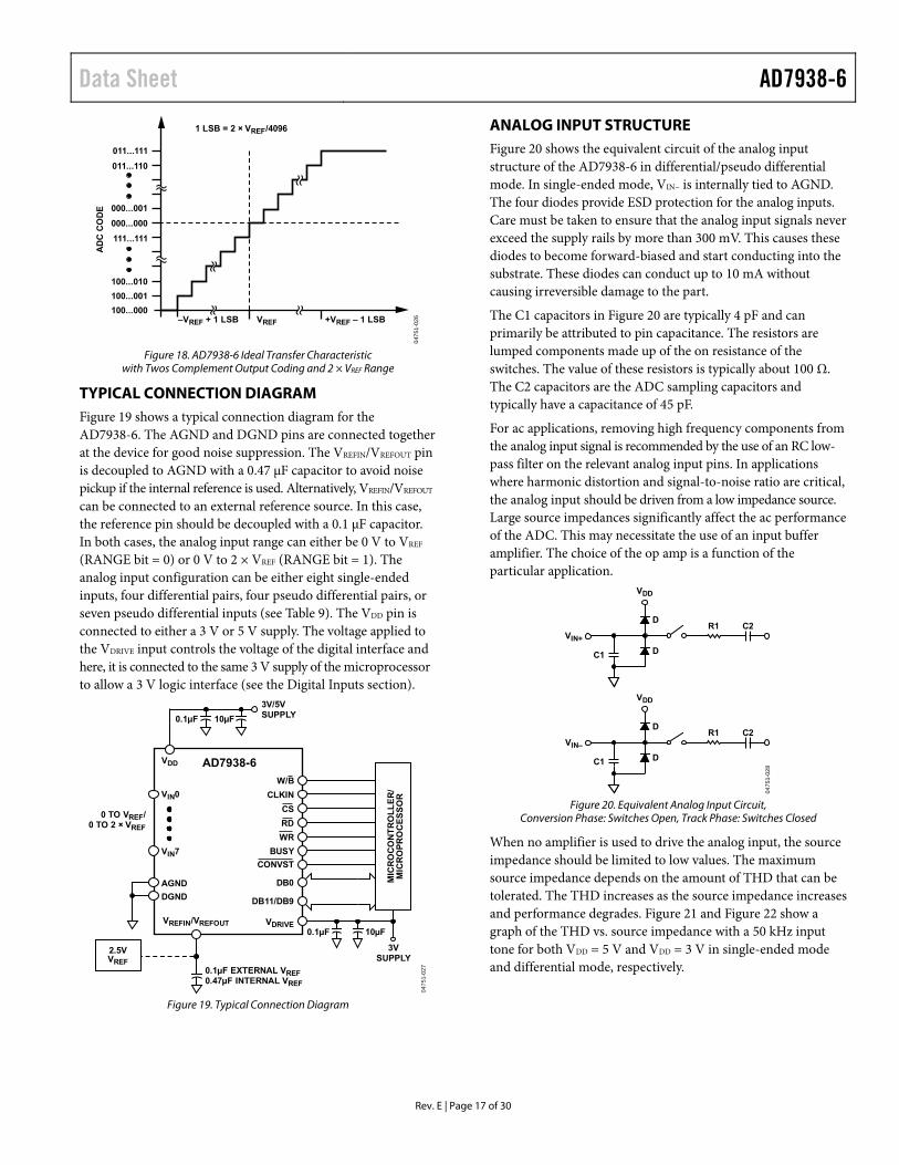
ANALOG INPUT STRUCTURE Figure 20 shows the equivalent circuit of the analog input structure of the AD7938-6 in differential/pseudo differential mode. In single-ended mode, VIN− is internally tied to AGND. The four diodes provide ESD protection for the analog inputs. Care must be taken to ensure that the analog input signals never exceed the supply rails by more than 300 mV. This causes these diodes to become forward-biased and start conducting into the substrate. These diodes can conduct up to 10 mA without causing irreversible damage to the part.
The C1 capacitors in Figure 20 are typically 4 pF and can primarily be attributed to pin capacitance. The resistors are lumped components made up of the on resistance of the switches. The value of these resistors is typically about 100 Ω. The C2 capacitors are the ADC sampling capacitors and typically have a capacitance of 45 pF.
For ac applications, removing high frequency components from the analog input signal is recommended by the use of an RC low-pass filter on the relevant analog input pins. In applications where harmonic distortion and signal-to-noise ratio are critical, the analog input should be driven from a low impedance source. Large source impedances significantly affect the ac performance of the ADC. This may necessitate the use of an input buffer amplifier. The choice of the op amp is a function of the particular application.
R1 C2VIN+
VDD
C1
D
D
0475
1-02
8
R1 C2VIN–
VDD
C1
D
D
Figure 20. Equivalent Analog Input Circuit,
Conversion Phase: Switches Open, Track Phase: Switches Closed
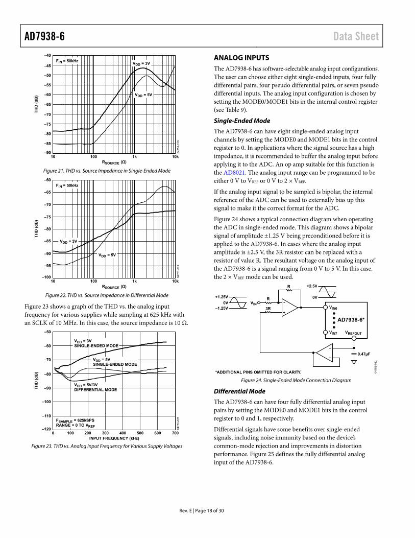
When no amplifier is used to drive the analog input, the source impedance should be limited to low values. The maximum source impedance depends on the amount of THD that can be tolerated. The THD increases as the source impedance increases and performance degrades. Figure 21 and Figure 22 show a graph of the THD vs. source impedance with a 50 kHz input tone for both VDD = 5 V and VDD = 3 V in single-ended mode and differential mode, respectively.
AD7938-6 Data Sheet
Rev. E | Page 18 of 30
RSOURCE (Ω)
TH
D (
dB
)
–40
–45
–50
–55
–80
–75
–70
–65
–60
–90
–85
10 100 1k 10k
0475
1-01
8
FIN = 50kHz
VDD = 5V
VDD = 3V
Figure 21. THD vs. Source Impedance in Single-Ended Mode
RSOURCE (Ω)
TH
D (
dB
)
–60
–80
–75
–70
–65
–100
–85
–90
–95
10 100 1k 10k
0475
1-01
9
FIN = 50kHz
VDD = 5V
VDD = 3V
Figure 22. THD vs. Source Impedance in Differential Mode
Figure 23 shows a graph of the THD vs. the analog input frequency for various supplies while sampling at 625 kHz with an SCLK of 10 MHz. In this case, the source impedance is 10 Ω.
INPUT FREQUENCY (kHz)
TH
D (
dB
)
–50
–60
–70
–80
–110
–100
–90
–1200 100 400200 300 600500 700
0475
1-02
0
FSAMPLE = 625kSPSRANGE = 0 TO VREF
VDD = 3VSINGLE-ENDED MODE
VDD = 5V/3VDIFFERENTIAL MODE
VDD = 5VSINGLE-ENDED MODE
Figure 23. THD vs. Analog Input Frequency for Various Supply Voltages
ANALOG INPUTS The AD7938-6 has software-selectable analog input configurations. The user can choose either eight single-ended inputs, four fully differential pairs, four pseudo differential pairs, or seven pseudo differential inputs. The analog input configuration is chosen by setting the MODE0/MODE1 bits in the internal control register (see Table 9).
Single-Ended Mode
The AD7938-6 can have eight single-ended analog input channels by setting the MODE0 and MODE1 bits in the control register to 0. In applications where the signal source has a high impedance, it is recommended to buffer the analog input before applying it to the ADC. An op amp suitable for this function is the AD8021. The analog input range can be programmed to be either 0 V to VREF or 0 V to 2 × VREF.
If the analog input signal to be sampled is bipolar, the internal reference of the ADC can be used to externally bias up this signal to make it the correct format for the ADC.
Figure 24 shows a typical connection diagram when operating the ADC in single-ended mode. This diagram shows a bipolar signal of amplitude ±1.25 V being preconditioned before it is applied to the AD7938-6. In cases where the analog input amplitude is ±2.5 V, the 3R resistor can be replaced with a resistor of value R. The resultant voltage on the analog input of the AD7938-6 is a signal ranging from 0 V to 5 V. In this case, the 2 × VREF mode can be used.
0.47µF
+1.25V
VIN
R
R
3R
0V–1.25V
+2.5V
0V
VIN0
VIN7 VREFOUT
AD7938-6*
*ADDITIONAL PINS OMITTED FOR CLARITY. 0475
1-03
1
Figure 24. Single-Ended Mode Connection Diagram
Differential Mode
The AD7938-6 can have four fully differential analog input pairs by setting the MODE0 and MODE1 bits in the control register to 0 and 1, respectively.
Differential signals have some benefits over single-ended signals, including noise immunity based on the device’s common-mode rejection and improvements in distortion performance. Figure 25 defines the fully differential analog input of the AD7938-6.

Data Sheet AD7938-6
Rev. E | Page 19 of 30
0475
1-03
2
VREFp-p
VIN+
VIN–VREFp-p
*ADDITIONAL PINS OMITTED FOR CLARITY.
AD7938-6*
COMMON-MODEVOLTAGE
Figure 25. Differential Input Definition
The amplitude of the differential signal is the difference between the signals applied to the VIN+ and VIN− pins in each differential pair (that is, VIN+ − VIN−). VIN+ and VIN− should be simultaneously driven by two signals each of amplitude VREF (or 2 × VREF, depending on the range chosen) that are 180° out of phase. The amplitude of the differential signal is therefore −VREF to +VREF peak-to-peak (that is, 2 × VREF). This is regardless of the common mode (CM). The common mode is the average of the two signals (that is, (VIN+ + VIN−)/2) and is therefore the voltage on which the two inputs are centered. This results in the span of each input being CM ± VREF/2. This voltage has to be set up externally and its range varies with the reference value VREF. As the value of VREF increases, the common-mode range decreases. When driving the inputs with an amplifier, the actual common-mode range is determined by the output voltage swing of the amplifier.
Figure 26 and Figure 27 show how the common-mode range typically varies with VREF for a 5 V power supply using the 0 V to VREF range or 2 × VREF range, respectively. The common mode must be in this range to guarantee the functionality of the AD7938-6.
When a conversion takes place, the common mode is rejected, resulting in a virtually noise-free signal of amplitude −VREF to +VREF corresponding to the digital codes of 0 to 4096. If the 2 × VREF range is used, the input signal amplitude extends from −2 VREF to +2 VREF after conversion.
VREF (V)
CO
MM
ON
-MO
DE
RA
NG
E (
V)
3.5
3.0
2.0
1.5
2.5
1.0
0.5
00 0.5 1.51.0 2.0 2.5 3.0
0475
1-03
3
TA = 25°C
Figure 26. Input Common-Mode Range vs. VREF (0 V to VREF Range, VDD = 5 V)
VREF (V)
CO
MM
ON
-MO
DE
RA
NG
E (
V)
4.5
4.0
3.0
1.5
2.0
2.5
3.5
1.0
0.5
00.1 0.6 1.61.1 2.1 2.6
0475
1-03
4
TA = 25°C
Figure 27. Input Common-Mode Range vs. VREF (2 × VREF Range, VDD = 5 V)
Driving Differential Inputs
Differential operation requires that VIN+ and VIN− be simultaneously driven with two equal signals that are 180° out of phase. The common mode must be set up externally and has a range that is determined by VREF, the power supply, and the particular amplifier used to drive the analog inputs. Differential modes of operation with either an ac or dc input provide the best THD performance over a wide frequency range. Since not all applications have a signal preconditioned for differential operation, there is often a need to perform single-ended-to-differential conversion.
Using an Op Amp Pair
An op amp pair can be used to directly couple a differential signal to one of the analog input pairs of the AD7938-6. The circuit configurations shown in Figure 28 and Figure 29 show how a dual op amp can be used to convert a single-ended signal into a differential signal for both a bipolar and unipolar input signal, respectively.
The voltage applied to Point A sets up the common-mode voltage. In both diagrams, it is connected in some way to the reference, but any value in the common-mode range can be input here to set up the common mode. A suitable dual op amp that can be used in this configuration to provide differential drive to the AD7938-6 is the AD8022.
It is advisable to take care when choosing the op amp; the selection depends on the required power supply and system performance objectives. The driver circuits in Figure 28 and Figure 29 are optimized for dc coupling applications requiring best distortion performance.
The differential op amp driver circuit in Figure 28 is configured to convert and level shift a single-ended, ground-referenced (bipolar) signal to a differential signal centered at the VREF level of the ADC.
The circuit configuration shown in Figure 29 converts a unipolar, single-ended signal into a differential signal.

AD7938-6 Data Sheet
Rev. E | Page 20 of 30
220Ω
10kΩ
2 × VREF p-p
GND440Ω
220Ω
220Ω
20kΩ
220Ω
27Ω
27Ω
V+
V–
V+
V–A
VIN+
VIN– VREF
AD7938-6
0.47µF
0475
1-03
5
3.75V
2.5V1.25V
3.75V
2.5V1.25V
Figure 28. Dual Op Amp Circuit to Convert a Single-Ended
Bipolar Signal into a Differential Unipolar Signal
10kΩ
VREF p-p
VREF
GND
440Ω
220Ω
220Ω
20kΩ
220Ω
27Ω
27Ω
V+
V–
V+
V–A
VIN+
VIN– VREF
AD7938-6
0.47µF
0475
1-03
6
3.75V
2.5V1.25V
3.75V
2.5V1.25V
Figure 29. Dual Op Amp Circuit to Convert a Single-Ended
Unipolar Signal into a Differential Signal
Another method of driving the AD7938-6 is to use the AD8138 (or equivalent) differential amplifier. The AD8138 can be used as a single-ended-to-differential amplifier or as a differential-to-differential amplifier. The device is as easy to use as an op amp and greatly simplifies differential signal amplification and driving.
Pseudo Differential Mode
The AD7938-6 can have four pseudo differential pairs (Pseudo Mode 1) or seven pseudo differential inputs (Pseudo Mode 2) by setting the MODE0 and MODE1 bits in the control register to 1, 0 and 1, 1, respectively. In the case of the four pseudo differential pairs, VIN+ is connected to the signal source, which must have an amplitude of VREF (or 2 × VREF depending on the range chosen) to make use of the full dynamic range of the part. A dc input is applied to the VIN− pin. The voltage applied to this input provides an offset from ground or a pseudo ground for the VIN+ input. In the case of the seven pseudo differential inputs, the seven analog input signals inputs are referred to a dc voltage applied to VIN7.
The benefit of pseudo differential inputs is that they separate the analog input signal ground from the ADC ground allowing dc common-mode voltages to be cancelled. The specified voltage range for the VIN− pin while in pseudo differential mode is −0.1 V to +0.4 V; however, typically this range can extend to −0.3 V to +0.7 V when VDD = 3 V, or −0.3 V to +1.8 V when VDD = 5 V. Figure 30 shows a connection diagram for pseudo differential mode.
VIN+
VIN–
VREF
AD7938-6*
*ADDITIONAL PINS OMITTED FOR CLARITY. 0475
1-03
7
VREF p-p
0.47µF
DC INPUTVOLTAGE
Figure 30. Pseudo Differential Mode Connection Diagram
ANALOG INPUT SELECTION As shown in Table 9, the user can set up their analog input configuration by setting the values in the MODE0 and MODE1 bits in the control register. Assuming the configuration has been chosen, there are different ways of selecting the analog input to be converted depending on the state of the SEQ and SHDW bits in the control register.
Traditional Multichannel Operation (SEQ = 0, SHDW = 0)
Any one of eight analog input channels or four pairs of channels can be selected for conversion in any order by setting the SEQ and SHDW bits in the control register to 0. The channel to be converted is selected by writing to the address bits, ADD2 to ADD0, in the control register to program the multiplexer prior to the conversion. This mode of operation is that of a traditional multichannel ADC where each data write selects the next channel for conversion. Figure 31 shows a flow chart of this mode of operation. The channel configurations are shown in Table 9.
POWER ON
WRITE TO THE CONTROL REGISTER TOSET UP OPERATING MODE, ANALOG INPUT
AND OUTPUT CONFIGURATIONSET SEQ = SHDW = 0. SELECT THE DESIRED
CHANNEL TO CONVERT (ADD2 TO ADD0).
ISSUE CONVST PULSE TO INITIATE A CONVERSIONON THE SELECTED CHANNEL.
INITIATE A READ CYCLE TO READ THE DATAFROM THE SELECTED CHANNEL.
INITIATE A WRITE CYCLE TO SELECT THE NEXTCHANNEL TO BE CONVERTED BY
CHANGING THE VALUES OF BITS ADD2 TO ADD0IN THE CONTROL REGISTER. SEQ = SHDW = 0.
0475
1-03
8
Figure 31. Traditional Multichannel Operation Flow Chart
Data Sheet AD7938-6
Rev. E | Page 21 of 30
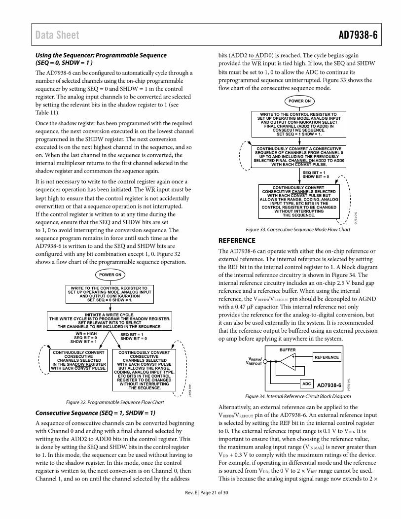
Using the Sequencer: Programmable Sequence (SEQ = 0, SHDW = 1 )
The AD7938-6 can be configured to automatically cycle through a number of selected channels using the on-chip programmable sequencer by setting SEQ = 0 and SHDW = 1 in the control register. The analog input channels to be converted are selected by setting the relevant bits in the shadow register to 1 (see Table 11).
Once the shadow register has been programmed with the required sequence, the next conversion executed is on the lowest channel programmed in the SHDW register. The next conversion executed is on the next highest channel in the sequence, and so on. When the last channel in the sequence is converted, the internal multiplexer returns to the first channel selected in the shadow register and commences the sequence again.
It is not necessary to write to the control register again once a sequencer operation has been initiated. The WR input must be kept high to ensure that the control register is not accidentally overwritten or that a sequence operation is not interrupted. If the control register is written to at any time during the sequence, ensure that the SEQ and SHDW bits are set to 1, 0 to avoid interrupting the conversion sequence. The sequence program remains in force until such time as the AD7938-6 is written to and the SEQ and SHDW bits are configured with any bit combination except 1, 0. Figure 32 shows a flow chart of the programmable sequence operation.
POWER ON
WRITE TO THE CONTROL REGISTER TOSET UP OPERATING MODE, ANALOG INPUT
AND OUTPUT CONFIGURATIONSET SEQ = 0 SHDW = 1.
INITIATE A WRITE CYCLE.THIS WRITE CYCLE IS TO PROGRAM THE SHADOW REGISTER.
SET RELEVANT BITS TO SELECTTHE CHANNELS TO BE INCLUDED IN THE SEQUENCE.
SEQ BIT = 1SHDW BIT = 0
CONTINUOUSLY CONVERTCONSECUTIVE
CHANNELS SELECTEDWITH EACH CONVST PULSEBUT ALLOWS THE RANGE,
CODING, ANALOG INPUT TYPE,ETC BITS IN THE CONTROLREGISTER TO BE CHANGED
WITHOUT INTERRUPTINGTHE SEQUENCE.
CONTINUOUSLY CONVERTCONSECUTIVE
CHANNELS SELECTEDIN THE SHADOW REGISTER
WITH EACH CONVST PULSE.
0475
1-03
9
WR = HIGHSEQ BIT = 0
SHDW BIT = 1
Figure 32. Programmable Sequence Flow Chart
Consecutive Sequence (SEQ = 1, SHDW = 1)
A sequence of consecutive channels can be converted beginning with Channel 0 and ending with a final channel selected by writing to the ADD2 to ADD0 bits in the control register. This is done by setting the SEQ and SHDW bits in the control register to 1. In this mode, the sequencer can be used without having to write to the shadow register. In this mode, once the control register is written to, the next conversion is on Channel 0, then Channel 1, and so on until the channel selected by the address
bits (ADD2 to ADD0) is reached. The cycle begins again provided the WR input is tied high. If low, the SEQ and SHDW bits must be set to 1, 0 to allow the ADC to continue its preprogrammed sequence uninterrupted. Figure 33 shows the flow chart of the consecutive sequence mode.
POWER ON
WRITE TO THE CONTROL REGISTER TOSET UP OPERATING MODE, ANALOG INPUT
AND OUTPUT CONFIGURATION SELECTFINAL CHANNEL (ADD2 TO ADD0) IN
CONSECUTIVE SEQUENCE.SET SEQ = 1 SHDW = 1.
CONTINUOUSLY CONVERT A CONSECUTIVESEQUENCE OF CHANNELS FROM CHANNEL 0
UP TO AND INCLUDING THE PREVIOUSLYSELECTED FINAL CHANNEL ON ADD2 TO ADD0
WITH EACH CONVST PULSE.
SEQ BIT = 1SHDW BIT = 0
CONTINUOUSLY CONVERTCONSECUTIVE CHANNELS SELECTED
WITH EACH CONVST PULSE BUTALLOWS THE RANGE, CODING, ANALOG
INPUT TYPE, ETC BITS IN THECONTROL REGISTER TO BE CHANGED
WITHOUT INTERRUPTINGTHE SEQUENCE.
0475
1-04
0
Figure 33. Consecutive Sequence Mode Flow Chart
REFERENCE The AD7938-6 can operate with either the on-chip reference or external reference. The internal reference is selected by setting the REF bit in the internal control register to 1. A block diagram of the internal reference circuitry is shown in Figure 34. The internal reference circuitry includes an on-chip 2.5 V band gap reference and a reference buffer. When using the internal reference, the VREFIN/VREFOUT pin should be decoupled to AGND with a 0.47 μF capacitor. This internal reference not only provides the reference for the analog-to-digital conversion, but it can also be used externally in the system. It is recommended that the reference output be buffered using an external precision op amp before applying it anywhere in the system.
REFERENCE
AD7938-6ADC
BUFFER04
751-
041
VREFIN/VREFOUT
Figure 34. Internal Reference Circuit Block Diagram
Alternatively, an external reference can be applied to the VREFIN/VREFOUT pin of the AD7938-6. An external reference input is selected by setting the REF bit in the internal control register to 0. The external reference input range is 0.1 V to VDD. It is important to ensure that, when choosing the reference value, the maximum analog input range (VIN MAX) is never greater than VDD + 0.3 V to comply with the maximum ratings of the device. For example, if operating in differential mode and the reference is sourced from VDD, the 0 V to 2 × VREF range cannot be used. This is because the analog input signal range now extends to 2 ×

AD7938-6 Data Sheet
Rev. E | Page 22 of 30
VDD, which exceeds maximum rating conditions. In the pseudo differential modes, the user must ensure that VREF + VIN− ≤ VDD when using the 0 V to VREF range, or when using the 2 × VREF range that 2 × VREF +VIN− ≤ VDD.
In all cases, the specified reference is 2.5 V.
The performance of the part with different reference values is shown in Figure 10 to Figure 12. The value of the reference sets the analog input span and the common-mode voltage range. Errors in the reference source result in gain errors in the AD7938-6 transfer function and add to specified full-scale errors on the part.
Table 12 lists examples of suitable voltage references from Analog Devices that can be used. Figure 35 shows a typical connection diagram for an external reference.
Table 12. Examples of Suitable Voltage References
Reference Output Voltage
Initial Accuracy (% Maximum)
Operating Current (μA)
AD780 2.5/3 0.04 1000 ADR421 2.5 0.04 500 ADR420 2.048 0.05 500
0475
1-04
2
1
AD780
NC8
2 +VIN NC7
3
GND
6
4
TEMP
5
O/PSELECT
TRIM
VOUT
VREF
2.5V
NC
NC
VDD
NC = NO CONNECT
10nF 0.1µF 0.1µF0.1µF
*ADDITIONAL PINS OMITTED FOR CLARITY.
AD7938-6*
Figure 35. Typical VREF Connection Diagram
Digital Inputs
The digital inputs applied to the AD7938-6 are not limited by the maximum ratings that limit the analog inputs. Instead, the digital inputs applied can go to 7 V and are not restricted by the VDD + 0.3 V limit as on the analog inputs.
Another advantage of the digital inputs not being restricted by the VDD + 0.3 V limit is the fact that power supply sequencing issues are avoided. If any of these inputs are applied before VDD, there is no risk of latch-up as there would be on the analog inputs if a signal greater than 0.3 V were applied prior to VDD.
VDRIVE Input
The AD7938-6 has a VDRIVE feature. VDRIVE controls the voltage at which the parallel interface operates. VDRIVE allows the ADC to easily interface to 3 V and 5 V processors.
For example, if the AD7938-6 is operated with an AVDD of 5 V and the VDRIVE pin is powered from a 3 V supply, the AD7938-6 has better dynamic performance with a VDD of 5 V while still being able to interface directly to 3 V processors. Care should be taken to ensure VDRIVE does not exceed VDD by more than 0.3 V (see the Absolute Maximum Ratings section).
Data Sheet AD7938-6
Rev. E | Page 23 of 30
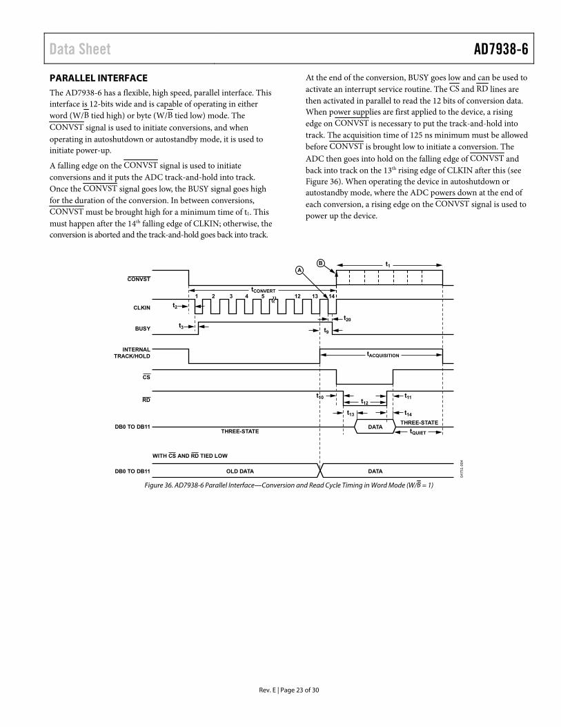
PARALLEL INTERFACE The AD7938-6 has a flexible, high speed, parallel interface. This interface is 12-bits wide and is capable of operating in either word (W/B tied high) or byte (W/B tied low) mode. The CONVST signal is used to initiate conversions, and when operating in autoshutdown or autostandby mode, it is used to initiate power-up.
A falling edge on the CONVST signal is used to initiate conversions and it puts the ADC track-and-hold into track. Once the CONVST signal goes low, the BUSY signal goes high for the duration of the conversion. In between conversions, CONVST must be brought high for a minimum time of t1. This must happen after the 14th falling edge of CLKIN; otherwise, the conversion is aborted and the track-and-hold goes back into track.
At the end of the conversion, BUSY goes low and can be used to activate an interrupt service routine. The CS and RD lines are then activated in parallel to read the 12 bits of conversion data. When power supplies are first applied to the device, a rising edge on CONVST is necessary to put the track-and-hold into track. The acquisition time of 125 ns minimum must be allowed before CONVST is brought low to initiate a conversion. The ADC then goes into hold on the falling edge of CONVST and back into track on the 13th rising edge of CLKIN after this (see Figure 36). When operating the device in autoshutdown or autostandby mode, where the ADC powers down at the end of each conversion, a rising edge on the CONVST signal is used to power up the device.
t2
t3
t20
t14
t11
t9
t13
t12
t10
tCONVERT
tACQUISITION
tQUIET
t1
1 2 3 4 5 12 13 14
BA
DATA
DATAOLD DATADB0 TO DB11
DB0 TO DB11
RD
CS
INTERNALTRACK/HOLD
BUSY
CLKIN
CONVST
THREE-STATE
THREE-STATE
WITH CS AND RD TIED LOW04
751-
004
Figure 36. AD7938-6 Parallel Interface—Conversion and Read Cycle Timing in Word Mode (W/B = 1)

AD7938-6 Data Sheet
Rev. E | Page 24 of 30
Reading Data from the AD7938-6
With the W/B pin tied logic high, the AD7938-6 interface operates in word mode. In this case, a single read operation from the device accesses the conversion data-word on Pin DB0 to Pin DB11. The DB8/HBEN pin assumes its DB8 function. With the W/B pin tied to logic low, the AD7938-6 interface operates in byte mode. In this case, the DB8/HBEN pin assumes its HBEN function. Conversion data from the AD7938-6 must be accessed in two read operations with eight bits of data provided on DB0 to DB7 for each of the read operations. The HBEN pin determines whether the read operation accesses the high byte or the low byte of the12-bit word. For a low byte read, DB0 to DB7 provide the eight LSBs of the 12-bit word. For a high byte read, DB0 to DB3 provide the four MSBs of the 12-bit word, DB4 to DB6 provide the Channel ID and DB7 is always a 0. Figure 36 shows the read cycle timing diagram for a 12-bit transfer. When operating in word mode, the HBEN input does not exist, and only the first read operation is required to access data from the device. When operating in byte mode, the two read cycles shown in Figure 37 are required to access the full data-word from the device.
The CS and RD signals are gated internally and the level is triggered active low. In either word mode or byte mode, CS and RD can be tied together as the timing specifications for t10 and t11 are 0 ns minimum. This means the bus would be constantly driven by the AD7938-6.
The data is placed onto the data bus a time, t13, after both CS and RD go low. The RD rising edge can be used to latch data out of the device. After a time, t14, the data lines become three-stated.
Alternatively, CS and RD can be tied permanently low and the conversion data is valid and placed onto the data bus a time, t9, before the falling edge of BUSY.
Note that if RD is pulsed during the conversion time this causes a degradation in linearity performance of approximately 0.25 LSB. Reading during conversion by way of tying CS and RD low does not cause any degradation.
t11t10
t13
t15 t15 t16t16
t14
t12
t17
LOW BYTE HIGH BYTEDB0 TO DB7
HBEN/DB8
RD
CS
0475
1-00
5
Figure 37. AD7938-6 Parallel Interface—Read Cycle Timing for Byte Mode Operation (W/B = 0)
Data Sheet AD7938-6
Rev. E | Page 25 of 30
Writing Data to the AD7938-6
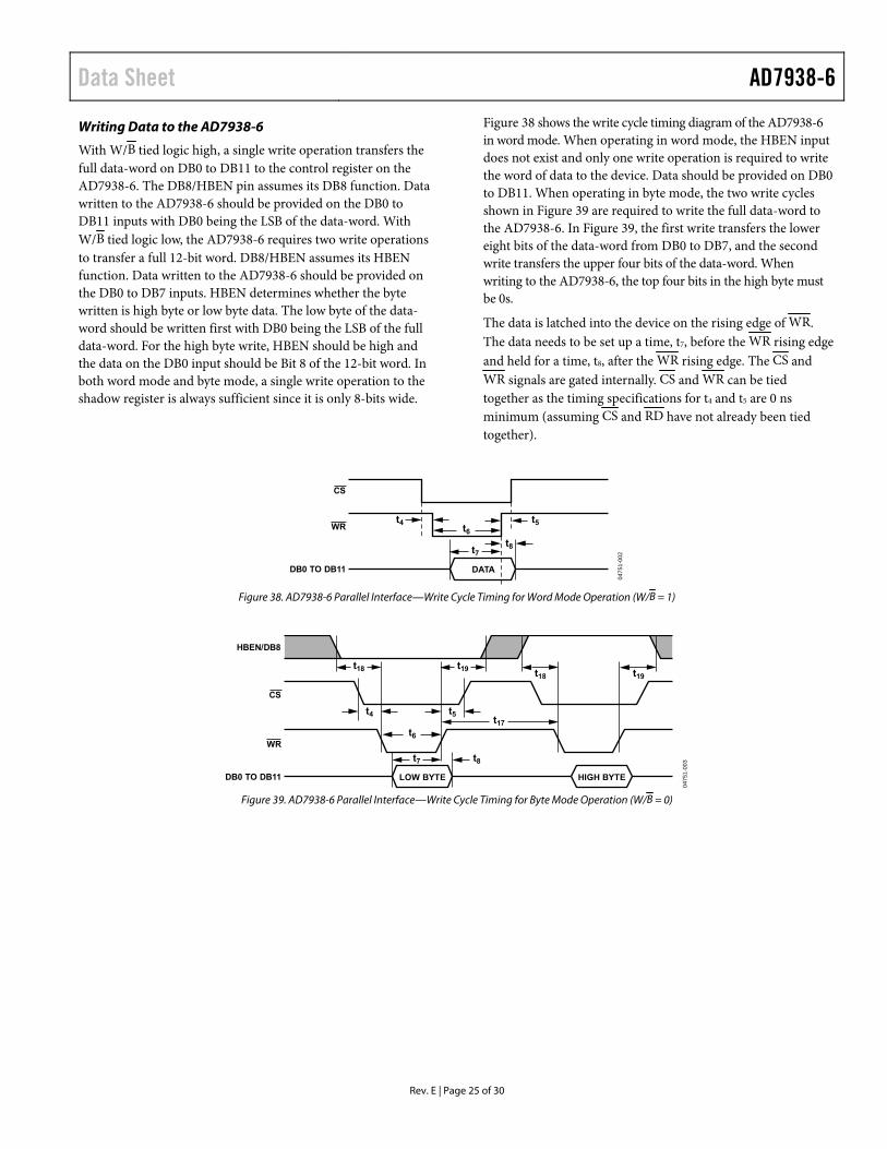
With W/B tied logic high, a single write operation transfers the full data-word on DB0 to DB11 to the control register on the AD7938-6. The DB8/HBEN pin assumes its DB8 function. Data written to the AD7938-6 should be provided on the DB0 to DB11 inputs with DB0 being the LSB of the data-word. With W/B tied logic low, the AD7938-6 requires two write operations to transfer a full 12-bit word. DB8/HBEN assumes its HBEN function. Data written to the AD7938-6 should be provided on the DB0 to DB7 inputs. HBEN determines whether the byte written is high byte or low byte data. The low byte of the data-word should be written first with DB0 being the LSB of the full data-word. For the high byte write, HBEN should be high and the data on the DB0 input should be Bit 8 of the 12-bit word. In both word mode and byte mode, a single write operation to the shadow register is always sufficient since it is only 8-bits wide.
Figure 38 shows the write cycle timing diagram of the AD7938-6 in word mode. When operating in word mode, the HBEN input does not exist and only one write operation is required to write the word of data to the device. Data should be provided on DB0 to DB11. When operating in byte mode, the two write cycles shown in Figure 39 are required to write the full data-word to the AD7938-6. In Figure 39, the first write transfers the lower eight bits of the data-word from DB0 to DB7, and the second write transfers the upper four bits of the data-word. When writing to the AD7938-6, the top four bits in the high byte must be 0s.
The data is latched into the device on the rising edge of WR. The data needs to be set up a time, t7, before the WR rising edge and held for a time, t8, after the WR rising edge. The CS and WR signals are gated internally. CS and WR can be tied together as the timing specifications for t4 and t5 are 0 ns minimum (assuming CS and RD have not already been tied together).
t8
t5
t7
t6
t4
DATADB0 TO DB11
WR
CS
0475
1-00
2
Figure 38. AD7938-6 Parallel Interface—Write Cycle Timing for Word Mode Operation (W/B = 1)
t5t4
t7
t18 t18 t19t19
t8
t6
t17
LOW BYTE HIGH BYTEDB0 TO DB11
HBEN/DB8
WR
CS04
751-
003
Figure 39. AD7938-6 Parallel Interface—Write Cycle Timing for Byte Mode Operation (W/B = 0)

AD7938-6 Data Sheet
Rev. E | Page 26 of 30
POWER MODES OF OPERATION The AD7938-6 has four different power modes of operation. These modes are designed to provide flexible power management options. Different options can be chosen to optimize the power dissipation/throughput rate ratio for differing applications. The mode of operation is selected by the power management bits, PM1 and PM0, in the control register, as detailed in Table 8. When power is first applied to the AD7938-6 an on-chip, power-on reset circuit ensures that the default power-up condition is normal mode.
Note that, after power-on, the track-and-hold is in hold mode and the first rising edge of CONVST places the track-and-hold into track mode.
Normal Mode (PM1 = PM0 = 0)
This mode is intended for the fastest throughput rate perfor-mance. The user does not have to worry about any power-up times associated with the AD7938-6 because it remains fully powered up at all times. At power-on reset, this mode is the default setting in the control register.
Autoshutdown (PM1 = 0; PM0 = 1)
In this mode of operation, the AD7938-6 automatically enters full shutdown at the end of each conversion, which is shown at Point A in Figure 36 and Figure 40. In shutdown mode, all internal circuitry on the device is powered down. The part retains information in the control register during shutdown. The track-and-hold also goes into hold at this point and remains in hold as long as the device is in shutdown. The AD7938-6 remains in shutdown mode until the next rising edge of CONVST (see Point B in Figure 36 and Figure 40). In order to keep the device in shutdown for as long as possible, CONVST should idle low between conversions, as shown in Figure 40. On this rising edge, the part begins to power-up and the track-and-hold returns to track mode. The power-up time required is 10 ms minimum regardless of whether the user is operating with the internal or external reference. The user should ensure that the power-up time has elapsed before initiating a conversion.
Autostandby (PM1 = 1; PM0 = 0)
In this mode of operation, the AD7938-6 automatically enters standby mode at the end of each conversion, which is shown as Point A in Figure 36. When this mode is entered, all circuitry on the AD7938-6 is powered down except for the reference and reference buffer. The track-and-hold goes into hold at this point also and remains in hold as long as the device is in standby. The part remains in standby until the next rising edge of CONVST powers up the device. The power-up time required depends on whether the internal or external reference is used. With an external reference, the power-up time required is a minimum of 600 ns, while when using the internal reference, the power-up time required is a minimum of 7 μs. The user should ensure this power-up time has elapsed before initiating another conversion as shown in Figure 40. This rising edge of CONVST also places the track-and-hold back into track mode.
Full Shutdown Mode (PM1 =1; PM0 = 1)
When this mode is programmed, all circuitry on the AD7938-6 is powered down upon completion of the write operation, that is, on the rising edge of WR. The track-and-hold enters hold mode at this point. The part retains the information in the control register while the part is in shutdown. The AD7938-6 remains in full shutdown mode, with the track-and-hold in hold mode, until the power management bits (PM1 and PM0) in the control register are changed. If a write to the control register occurs while the part is in full shutdown mode, and the power management bits are changed to PM0 = PM1 = 0, that is, normal mode, the part begins to power-up on the WR rising edge and the track-and-hold returns to track. To ensure the part is fully powered up before a conversion is initiated, the power-up time of 10 ms minimum should be allowed before the next CONVST falling edge; otherwise, invalid data is read.
Note that all power-up times quoted apply with a 470 nF capacitor on the VREFIN pin.
tPOWER-UP
1 114 14
BUSY
CLKIN
CONVST
0475
1-04
9
A B
Figure 40. Autoshutdown/Autostandby Mode
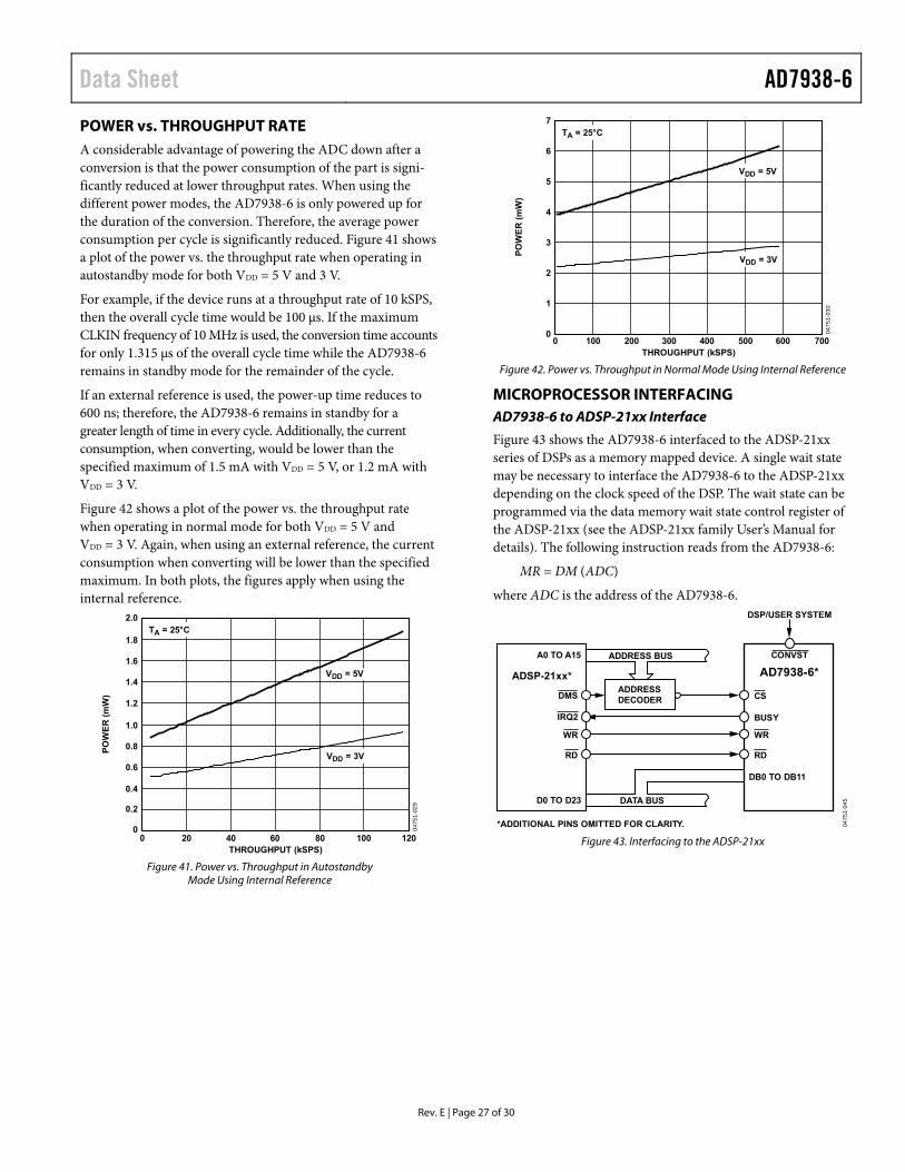
Data Sheet AD7938-6
Rev. E | Page 27 of 30
POWER vs. THROUGHPUT RATE A considerable advantage of powering the ADC down after a conversion is that the power consumption of the part is signi-ficantly reduced at lower throughput rates. When using the different power modes, the AD7938-6 is only powered up for the duration of the conversion. Therefore, the average power consumption per cycle is significantly reduced. Figure 41 shows a plot of the power vs. the throughput rate when operating in autostandby mode for both VDD = 5 V and 3 V.
For example, if the device runs at a throughput rate of 10 kSPS, then the overall cycle time would be 100 μs. If the maximum CLKIN frequency of 10 MHz is used, the conversion time accounts for only 1.315 μs of the overall cycle time while the AD7938-6 remains in standby mode for the remainder of the cycle.
If an external reference is used, the power-up time reduces to 600 ns; therefore, the AD7938-6 remains in standby for a greater length of time in every cycle. Additionally, the current consumption, when converting, would be lower than the specified maximum of 1.5 mA with VDD = 5 V, or 1.2 mA with VDD = 3 V.
Figure 42 shows a plot of the power vs. the throughput rate when operating in normal mode for both VDD = 5 V and VDD = 3 V. Again, when using an external reference, the current consumption when converting will be lower than the specified maximum. In both plots, the figures apply when using the internal reference.
THROUGHPUT (kSPS)
PO
WE
R (
mW
)
2.0
0.8
1.0
1.2
1.4
1.6
1.8
0
0.6
0.4
0.2
0 20 40 60 80 120100
0475
1-02
9
TA = 25°C
VDD = 5V
VDD = 3V
Figure 41. Power vs. Throughput in Autostandby
Mode Using Internal Reference
THROUGHPUT (kSPS)
PO
WE
R (
mW
)
7
1
2
3
4
5
6
00 100 200 300 400 500 700600
0475
1-03
0
TA = 25°C
VDD = 5V
VDD = 3V
Figure 42. Power vs. Throughput in Normal Mode Using Internal Reference
MICROPROCESSOR INTERFACING AD7938-6 to ADSP-21xx Interface
Figure 43 shows the AD7938-6 interfaced to the ADSP-21xx series of DSPs as a memory mapped device. A single wait state may be necessary to interface the AD7938-6 to the ADSP-21xx depending on the clock speed of the DSP. The wait state can be programmed via the data memory wait state control register of the ADSP-21xx (see the ADSP-21xx family User’s Manual for details). The following instruction reads from the AD7938-6:
MR = DM (ADC)
where ADC is the address of the AD7938-6.
AD7938-6*ADSP-21xx*
WR
RD
DB0 TO DB11
D0 TO D23
A0 TO A15
DMS
IRQ2 BUSY
CS
CONVST
DSP/USER SYSTEM
WR
RD
*ADDITIONAL PINS OMITTED FOR CLARITY.
ADDRESS BUS
DATA BUS
ADDRESSDECODER
0475
1-04
5
Figure 43. Interfacing to the ADSP-21xx
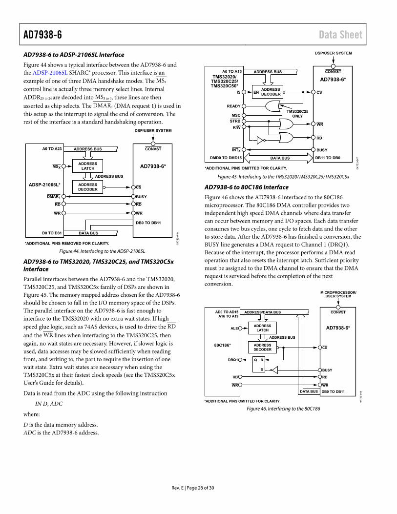
AD7938-6 Data Sheet
Rev. E | Page 28 of 30
AD7938-6 to ADSP-21065L Interface
Figure 44 shows a typical interface between the AD7938-6 and the ADSP-21065L SHARC® processor. This interface is an example of one of three DMA handshake modes. The MSx control line is actually three memory select lines. Internal ADDR25 to 24 are decoded into MS3 to 0, these lines are then asserted as chip selects. The DMAR1 (DMA request 1) is used in this setup as the interrupt to signal the end of conversion. The rest of the interface is a standard handshaking operation.
AD7938-6*
ADSP-21065L*
WR
DB0 TO DB11
D0 TO D31
A0 TO A23
MSX
DMAR1 BUSY
CS
CONVST
DSP/USER SYSTEM
WR
RDRD
*ADDITIONAL PINS REMOVED FOR CLARITY.
ADDRESS BUS
ADDRESS BUS
DATA BUS
ADDRESSLATCH
ADDRESSDECODER
0475
1-04
6
Figure 44. Interfacing to the ADSP-21065L
AD7938-6 to TMS32020, TMS320C25, and TMS320C5x Interface
Parallel interfaces between the AD7938-6 and the TMS32020, TMS320C25, and TMS320C5x family of DSPs are shown in Figure 45. The memory mapped address chosen for the AD7938-6 should be chosen to fall in the I/O memory space of the DSPs. The parallel interface on the AD7938-6 is fast enough to interface to the TMS32020 with no extra wait states. If high speed glue logic, such as 74AS devices, is used to drive the RD and the WR lines when interfacing to the TMS320C25, then again, no wait states are necessary. However, if slower logic is used, data accesses may be slowed sufficiently when reading from, and writing to, the part to require the insertion of one wait state. Extra wait states are necessary when using the TMS320C5x at their fastest clock speeds (see the TMS320C5x User’s Guide for details).
Data is read from the ADC using the following instruction
IN D, ADC
where:
D is the data memory address. ADC is the AD7938-6 address.
AD7938-6*TMS32020/TMS320C25/TMS320C50*
WR
RD
DB11 TO DB0DMD0 TO DMD15
A0 TO A15
IS
READY
INTX BUSY
CSEN
CONVST
DSP/USER SYSTEM
TMS320C25ONLY
R/W
STRB
*ADDITIONAL PINS OMITTED FOR CLARITY.
ADDRESS BUS
DATA BUS
ADDRESSDECODER
0475
1-04
7
MSC
Figure 45. Interfacing to the TMS32020/TMS320C25/TMS320C5x
AD7938-6 to 80C186 Interface
Figure 46 shows the AD7938-6 interfaced to the 80C186 microprocessor. The 80C186 DMA controller provides two independent high speed DMA channels where data transfer can occur between memory and I/O spaces. Each data transfer consumes two bus cycles, one cycle to fetch data and the other to store data. After the AD7938-6 has finished a conversion, the BUSY line generates a DMA request to Channel 1 (DRQ1). Because of the interrupt, the processor performs a DMA read operation that also resets the interrupt latch. Sufficient priority must be assigned to the DMA channel to ensure that the DMA request is serviced before the completion of the next conversion.
AD7938-6*
80C186*
WR
DB0 TO DB11
AD0 TO AD15A16 TO A19
ALE
DRQ1
BUSY
CS
Q R
S
CONVST
MICROPROCESSOR/USER SYSTEM
WR
RDRD
*ADDITIONAL PINS OMITTED FOR CLARITY
ADDRESS/DATA BUS
ADDRESS BUS
DATA BUS
ADDRESSLATCH
ADDRESSDECODER
0475
1-04
8
Figure 46. Interfacing to the 80C186

Data Sheet AD7938-6
Rev. E | Page 29 of 30
APPLICATION HINTS GROUNDING AND LAYOUT The printed circuit board that houses the AD7938-6 should be designed so that the analog and digital sections are separated and confined to certain areas of the board. This facilitates the use of ground planes that can be easily separated. Generally, a minimum etch technique is best for ground planes since it gives the best shielding. Digital and analog ground planes should be joined in only one place, and the connection should be a star ground point established as close to the ground pins on the AD7938-6 as possible. Avoid running digital lines under the device as this couples noise onto the die. The analog ground plane should be allowed to run under the AD7938-6 to avoid noise coupling. The power supply lines to the AD7938-6 should use as large a trace as possible to provide low impedance paths and reduce the effects of glitches on the power supply line.
Fast switching signals, such as clocks, should be shielded with digital ground to avoid radiating noise to other sections of the board, and clock signals should never run near the analog inputs. Avoid crossover of digital and analog signals. Traces on opposite sides of the board should run at right angles to each other. This reduces the effects of feedthrough through the board. A microstrip technique is by far the best but is not always possible with a double-sided board. In this technique, the component side of the board is dedicated to ground planes, while signals are placed on the solder side.
Good decoupling is also important. All analog supplies should be decoupled with 10 µF tantalum capacitors in parallel with 0.1 µF capacitors to GND. To achieve the best performance from these decoupling components, they must be placed as close as possible to the device, ideally right up against the device. The 0.1 µF capacitors should have low effective series resistance (ESR) and effective series inductance (ESI), such as the common ceramic types or surface-mount types, which provide a low impedance path to ground at high frequencies to handle transient currents due to internal logic switching.
PCB DESIGN GUIDELINES FOR CHIP SCALE PACKAGE The lands on the chip scale package (CP-32-2) are rectangular. The printed circuit board pad for these should be 0.1 mm longer than the package land length and 0.05 mm wider than the package land width. The land should be centered on the pad. This ensures that the solder joint size is maximized. The bottom of the chip scale package has a thermal pad. The thermal pad on the printed circuit board should be at least as large as this exposed pad. On the printed circuit board, there should be a clearance of at least 0.25 mm between the thermal pad and the inner edges of the pad pattern. This ensures that shorting is avoided. Thermal vias can be used on the printed circuit board thermal pad to improve thermal performance of the package. If vias are used, they should be incorporated in the thermal pad at 1.2 mm pitch grid. The via diameter should be between 0.3 mm and 0.33 mm, and the via barrel should be plated with 1 oz. copper to plug the via. The user should connect the printed circuit board thermal pad to AGND.
EVALUATING THE AD7938-6 PERFORMANCE The recommended layout for the AD7938-6 is outlined in the evaluation board documentation. The evaluation board package includes a fully assembled and tested evaluation board, documentation, and software for controlling the board from the PC via the evaluation board controller. The evaluation board controller can be used in conjunction with the AD7938-6 evaluation board, as well as many other Analog Devices evaluation boards ending in the CB designator, to demonstrate/evaluate the ac and dc performance of the AD7938-6.
The software allows the user to perform ac (fast Fourier transform) and dc (histogram of codes) tests on the AD7938-6. The software and documentation are on the CD that ships with the evaluation board.
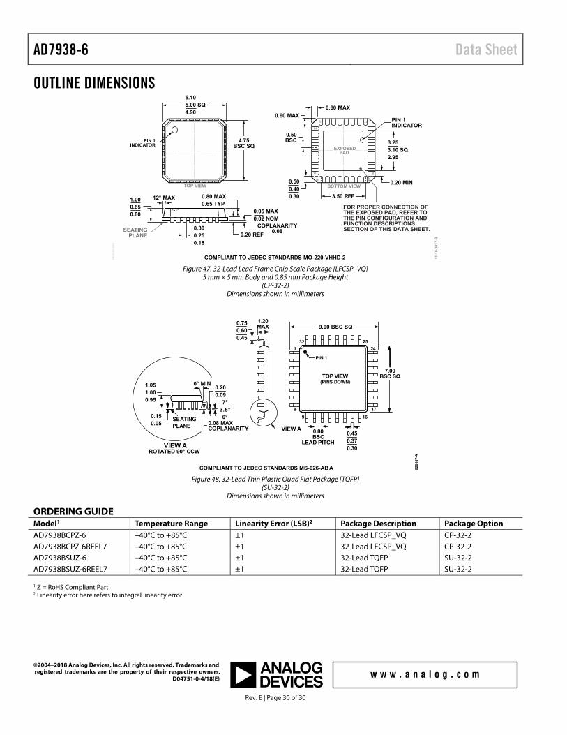
AD7938-6 Data Sheet
Rev. E | Page 30 of 30
OUTLINE DIMENSIONS
3.253.10 SQ2.95
COMPLIANT TO JEDEC STANDARDS MO-220-VHHD-2
1
32
8
9
25
24
17
16
COPLANARITY0.08
3.50 REF
0.50BSC
PIN 1INDICATOR
PIN 1INDICATOR
0.300.250.18
0.20 REF
12° MAX 0.80 MAX0.65 TYP
1.000.850.80 0.05 MAX
0.02 NOM
0.500.400.30
4.75BSC SQ
0.60 MAX
0.60 MAX
0.20 MIN
11-1
0-20
17-
B
TOP VIEW
EXPOSEDPAD
BOTTOM VIEW
5.105.00 SQ4.90
SEATINGPLANE
PK
G-0
01
05
0
FOR PROPER CONNECTION OFTHE EXPOSED PAD, REFER TOTHE PIN CONFIGURATION ANDFUNCTION DESCRIPTIONSSECTION OF THIS DATA SHEET.
Figure 47. 32-Lead Lead Frame Chip Scale Package [LFCSP_VQ]
5 mm × 5 mm Body and 0.85 mm Package Height (CP-32-2)
Dimensions shown in millimeters
COMPLIANT TO JEDEC STANDARDS MS-026-ABA
0.450.370.30
0.80BSC
LEAD PITCH
7.00BSC SQ
9.00 BSC SQ
1 24
2532
8
9
17
16
1.20MAX
0.750.600.45
1.051.000.95
0.200.09
0.08 MAXCOPLANARITY
SEATINGPLANE
0° MIN
7°3.5°0°0.15
0.05
VIEW AROTATED 90° CCW
VIEW A
PIN 1
TOP VIEW(PINS DOWN)
020
607-
A
Figure 48. 32-Lead Thin Plastic Quad Flat Package [TQFP]
(SU-32-2) Dimensions shown in millimeters
ORDERING GUIDE Model1 Temperature Range Linearity Error (LSB)2 Package Description Package Option AD7938BCPZ-6 –40°C to +85°C ±1 32-Lead LFCSP_VQ CP-32-2 AD7938BCPZ-6REEL7 –40°C to +85°C ±1 32-Lead LFCSP_VQ CP-32-2 AD7938BSUZ-6 –40°C to +85°C ±1 32-Lead TQFP SU-32-2 AD7938BSUZ-6REEL7 –40°C to +85°C ±1 32-Lead TQFP SU-32-2 1 Z = RoHS Compliant Part. 2 Linearity error here refers to integral linearity error.
©2004–2018 Analog Devices, Inc. All rights reserved. Trademarks and registered trademarks are the property of their respective owners. D04751-0-4/18(E)