8-bit - microchip technologyww1.microchip.com/downloads/en/devicedoc/doc1062.pdf · – up to 4...
TRANSCRIPT

8-bit Microcontroller with 2K Bytes of Flash
ATtiny28LATtiny28V
Rev. 1062F–AVR–07/06
Features• Utilizes the AVR® RISC Architecture• AVR – High-performance and Low-power RISC Architecture
– 90 Powerful Instructions – Most Single Clock Cycle Execution– 32 x 8 General-purpose Working Registers– Up to 4 MIPS Throughput at 4 MHz
• Nonvolatile Program Memory– 2K Bytes of Flash Program Memory– Endurance: 1,000 Write/Erase Cycles– Programming Lock for Flash Program Data Security
• Peripheral Features– Interrupt and Wake-up on Low-level Input– One 8-bit Timer/Counter with Separate Prescaler– On-chip Analog Comparator– Programmable Watchdog Timer with On-chip Oscillator– Built-in High-current LED Driver with Programmable Modulation
• Special Microcontroller Features– Low-power Idle and Power-down Modes– External and Internal Interrupt Sources– Power-on Reset Circuit with Programmable Start-up Time– Internal Calibrated RC Oscillator
• Power Consumption at 1 MHz, 2V, 25°C– Active: 3.0 mA– Idle Mode: 1.2 mA– Power-down Mode: <1 µA
• I/O and Packages– 11 Programmable I/O Lines, 8 Input Lines and a High-current LED Driver– 28-lead PDIP, 32-lead TQFP, and 32-pad MLF
• Operating Voltages– VCC: 1.8V - 5.5V for the ATtiny28V– VCC: 2.7V - 5.5V for the ATtiny28L
• Speed Grades– 0 - 1.2 MHz for the ATtiny28V– 0 - 4 MHz For the ATtiny28L
Pin ConfigurationsPDIP
RESETPD0PD1PD2PD3PD4VCCGND
XTAL1XTAL2
PD5PD6PD7
(AIN0) PB0
PA0PA1PA3PA2 (IR)PB7PB6GNDNCVCCPB5PB4 (INT1)PB3 (INT0)PB2 (T0)PB1 (AIN1)
1234567891011121314
2827262524232221201918171615
TQFP/QFN/MLF
12345678
2423222120191817
PD3PD4NC
VCCGND
NCXTAL1XTAL2
PB7PB6NCGNDNCNCVCCPB5
32 31 30 29 28 27 26 25
9 10 11 12 13 14 15 16
PD
5P
D6
PD
7(A
IN0)
PB
0(A
IN1)
PB
1(T
0) P
B2
(IN
T0)
PB
3(I
NT
1) P
B4
PD
2P
D1
PD
0R
ES
ET
PA
0P
A1
PA
3P
A2
(IR
)
1

Description The ATtiny28 is a low-power CMOS 8-bit microcontroller based on the AVR RISC archi-tecture. By executing powerful instructions in a single clock cycle, the ATtiny28 achievesthroughputs approaching 1 MIPS per MHz, allowing the system designer to optimizepower consumption versus processing speed. The AVR core combines a rich instructionset with 32 general-purpose working registers. All the 32 registers are directly con-nected to the Arithmetic Logic Unit (ALU), allowing two independent registers to beaccessed in one single instruction executed in one clock cycle. The resulting architec-ture is more code efficient while achieving throughputs up to ten times faster thanconventional CISC microcontrollers.
Block Diagram Figure 1. The ATtiny28 Block Diagram
The ATtiny28 provides the following features: 2K bytes of Flash, 11 general-purpose I/Olines, 8 input lines, a high-current LED driver, 32 general-purpose working registers, an8-bit timer/counter, internal and external interrupts, programmable Watchdog Timer withinternal oscillator and 2 software-selectable power-saving modes. The Idle Mode stopsthe CPU while allowing the timer/counter and interrupt system to continue functioning.The Power-down mode saves the register contents but freezes the oscillator, disablingall other chip functions until the next interrupt or hardware reset. The wake-up or inter-
PROGRAMCOUNTER
INTERNALOSCILLATOR
WATCHDOG TIMER
STACKPOINTER
PROGRAMFLASH
MCU CONTROLREGISTER
GENERALPURPOSE
REGISTERS
INSTRUCTIONREGISTER
TIMER/COUNTER
INSTRUCTIONDECODER
DATA REGISTERPORTB
PROGRAMMINGLOGIC
TIMING ANDCONTROL
INTERRUPTUNIT
STATUSREGISTER
ALU
PORTB
VCC
GND
CONTROLLINES
+ -
AN
ALO
GC
OM
PA
RA
TO
R8-BIT DATA BUS
Z
OSCILLATOR
PORTD
DATA REGISTERPORTA
PORTA
PORTA CONTROLREGISTER
XTAL2XTAL1
RESET
HARDWARESTACK
DATA REGISTERPORTD
DATA DIRREG. PORTD
HARDWAREMODULATOR
INTERNALCALIBRATEDOSCILLATOR
2 ATtiny28L/V 1062F–AVR–07/06
ATtiny28L/V
rupt on low-level input feature enables the ATtiny28 to be highly responsive to externalevents, still featuring the lowest power consumption while in the power-down modes.
The device is manufactured using Atmel’s high-density, nonvolatile memory technology.By combining an enhanced RISC 8-bit CPU with Flash on a monolithic chip, the AtmelATtiny28 is a powerful microcontroller that provides a highly flexible and cost-effectivesolution to many embedded control applications. The ATtiny28 AVR is supported with afull suite of program and system development tools including: macro assemblers, pro-gram debugger/simulators, in-circuit emulators and evaluation kits.
Pin Descriptions
VCC Supply voltage pin.
GND Ground pin.
Port A (PA3..PA0) Port A is a 4-bit I/O port. PA2 is output-only and can be used as a high-current LEDdriver. At VCC = 2.0V, the PA2 output buffer can sink 25 mA. PA3, PA1 and PA0 arebi-directional I/O pins with internal pull-ups (selected for each bit). The port pins are tri-stated when a reset condition becomes active, even if the clock is not running.
Port B (PB7..PB0) Port B is an 8-bit input port with internal pull-ups (selected for all Port B pins). Port Bpins that are externally pulled low will source current if the pull-ups are activated.
Port B also serves the functions of various special features of the ATtiny28 as listed onpage 27. If any of the special features are enabled, the pull-up(s) on the correspondingpin(s) is automatically disabled. The port pins are tri-stated when a reset conditionbecomes active, even if the clock is not running.
Port D (PD7..PD0) Port D is an 8-bit I/O port. Port pins can provide internal pull-up resistors (selected foreach bit). The port pins are tri-stated when a reset condition becomes active, even if theclock is not running.
XTAL1 Input to the inverting oscillator amplifier and input to the internal clock operating circuit.
XTAL2 Output from the inverting oscillator amplifier.
RESET Reset input. An external reset is generated by a low level on the RESET pin. Resetpulses longer than 50 ns will generate a reset, even if the clock is not running. Shorterpulses are not guaranteed to generate a reset.
Figure 2.
31062F–AVR–07/06
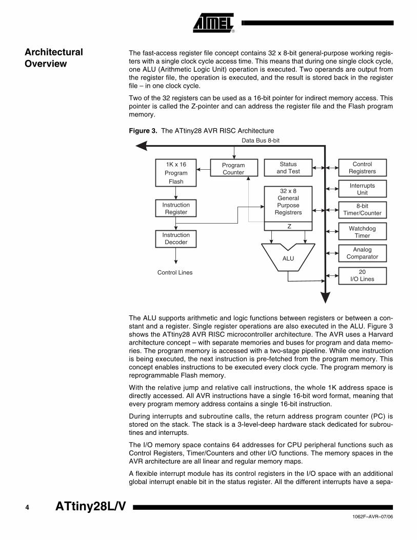
Architectural Overview
The fast-access register file concept contains 32 x 8-bit general-purpose working regis-ters with a single clock cycle access time. This means that during one single clock cycle,one ALU (Arithmetic Logic Unit) operation is executed. Two operands are output fromthe register file, the operation is executed, and the result is stored back in the registerfile – in one clock cycle.
Two of the 32 registers can be used as a 16-bit pointer for indirect memory access. Thispointer is called the Z-pointer and can address the register file and the Flash programmemory.
Figure 3. The ATtiny28 AVR RISC Architecture
The ALU supports arithmetic and logic functions between registers or between a con-stant and a register. Single register operations are also executed in the ALU. Figure 3shows the ATtiny28 AVR RISC microcontroller architecture. The AVR uses a Harvardarchitecture concept – with separate memories and buses for program and data memo-ries. The program memory is accessed with a two-stage pipeline. While one instructionis being executed, the next instruction is pre-fetched from the program memory. Thisconcept enables instructions to be executed every clock cycle. The program memory isreprogrammable Flash memory.
With the relative jump and relative call instructions, the whole 1K address space isdirectly accessed. All AVR instructions have a single 16-bit word format, meaning thatevery program memory address contains a single 16-bit instruction.
During interrupts and subroutine calls, the return address program counter (PC) isstored on the stack. The stack is a 3-level-deep hardware stack dedicated for subrou-tines and interrupts.
The I/O memory space contains 64 addresses for CPU peripheral functions such asControl Registers, Timer/Counters and other I/O functions. The memory spaces in theAVR architecture are all linear and regular memory maps.
A flexible interrupt module has its control registers in the I/O space with an additionalglobal interrupt enable bit in the status register. All the different interrupts have a sepa-
Control Lines
ALU
Data Bus 8-bit
1K x 16Program
Flash
InstructionRegister
InstructionDecoder
ProgramCounter
Statusand Test
32 x 8GeneralPurpose
Registrers
Z
ControlRegistrers
InterruptsUnit
8-bitTimer/Counter
WatchdogTimer
AnalogComparator
20I/O Lines
4 ATtiny28L/V 1062F–AVR–07/06

ATtiny28L/V
rate in terrupt vector in the interrupt vector table at the beginning of theprogram memory. The different interrupts have priority in accordance with their interruptvector position. The lower the interrupt vector address, the higher the priority.
ALU – Arithmetic Logic Unit
The high-performance AVR ALU operates in direct connection with all the 32 general-purpose working registers. Within a single clock cycle, ALU operations between regis-ters in the register file are executed. The ALU operations are divided into three maincategories – arithmetic, logic and bit functions. Some microcontrollers in the AVR prod-uct family feature a hardware multiplier in the arithmetic part of the ALU.
Subroutine and Interrupt Hardware Stack
The ATtiny28 uses a 3-level-deep hardware stack for subroutines and interrupts. Thehardware stack is 10 bits wide and stores the program counter (PC) return addresswhile subroutines and interrupts are executed.
RCALL instructions and interrupts push the PC return address onto stack level 0, andthe data in the other stack levels 1 - 2 are pushed one level deeper in the stack. When aRET or RETI instruction is executed the returning PC is fetched from stack level 0, andthe data in the other stack levels 1 - 2 are popped one level in the stack.
If more than three subsequent subroutine calls or interrupts are executed, the first val-ues written to the stack are overwritten.
General-purpose Register File
Figure 4 shows the structure of the 32 general-purpose registers in the CPU.
Figure 4. AVR CPU General-purpose Working Registers
All the register operating instructions in the instruction set have direct and single cycleaccess to all registers. The only exception are the five constant arithmetic and logicinstructions SBCI, SUBI, CPI, ANDI and ORI between a constant and a register and theLDI instruction for load immediate constant data. These instructions apply to the secondhalf of the registers in the register file – R16..R31. The general SBC, SUB, CP, AND,OR and all other operations between two registers or on a single register apply to theentire register file.
Registers 30 and 31 form a 16-bit pointer (the Z-pointer), which is used for indirect Flashmemory and register file access. When the register file is accessed, the contents of R31are discarded by the CPU.
7 0
R0
R1
R2
General …
Purpose …
Working R28
Registers R29
R30 (Z-Register low byte)
R31(Z-Register high byte)
51062F–AVR–07/06

Status Register
Status Register – SREG The AVR status register (SREG) at I/O space location $3F is defined as:
• Bit 7 – I: Global Interrupt Enable
The global interrupt enable bit must be set (one) for the interrupts to be enabled. Theindividual interrupt enable control is then performed in separate control registers. If theglobal interrupt enable register is cleared (zero), none of the interrupts are enabled inde-pendent of the individual interrupt enable settings. The I-bit is cleared by hardware afteran interrupt has occurred, and is set by the RETI instruction to enable subsequentinterrupts.
• Bit 6 – T: Bit Copy Storage
The bit copy instructions BLD (Bit LoaD) and BST (Bit STore) use the T-bit as sourceand destination for the operated bit. A bit from a register in the register file can be copiedinto T by the BST instruction, and a bit in T can be copied into a bit in a register in theregister file by the BLD instruction.
• Bit 5 – H: Half-carry Flag
The half-carry flag H indicates a half-carry in some arithmetic operations. See theInstruction Set description for detailed information.
• Bit 4 – S: Sign Bit, S = N ⊕ V
The S-bit is always an exclusive or between the negative flag N and the two’s comple-ment overflow flag V. See the Instruction Set description for detailed information.
• Bit 3 – V: Two’s Complement Overflow Flag
The two’s complement overflow flag V supports two’s complement arithmetic. See theInstruction Set description for detailed information.
• Bit 2 – N: Negative Flag
The negative flag N indicates a negative result from an arithmetical or logical operation.See the Instruction Set description for detailed information.
• Bit 1 – Z: Zero Flag
The zero flag Z indicates a zero result from an arithmetical or logical operation. See theInstruction Set description for detailed information.
• Bit 0 – C: Carry Flag
The carry flag C indicates a carry in an arithmetical or logical operation. See the Instruc-tion Set description for detailed information.
Note that the status register is not automatically stored when entering an interrupt rou-tine and restored when returning from an interrupt routine. This must be handled bysoftware.
Bit 7 6 5 4 3 2 1 0
$3F I T H S V N Z C SREG
Read/Write R/W R/W R/W R/W R/W R/W R/W R/W
Initial Value 0 0 0 0 0 0 0 0
6 ATtiny28L/V 1062F–AVR–07/06

ATtiny28L/V
System Clock and Clock Options
The device has the following clock source options, selectable by Flash Fuse bits asshown in Table 1.
Note: “1” means unprogrammed, “0” means programmed.
The various choices for each clocking option give different start-up times as shown inTable 5 on page 16.
Internal RC Oscillator The internal RC oscillator option is an on-chip calibrated oscillator running at a nominalfrequency of 1.2 MHz. If selected, the device can operate with no external components.The device is shipped with this option selected.
Calibrated Internal RC Oscillator
The calibrated internal oscillator provides a fixed 1.2 MHz (nominal) clock at 3V and25°C. This clock may be used as the system clock. This oscillator can be calibrated bywriting the calibration byte to the OSCCAL register. When this oscillator is used as thechip clock, the Watchdog oscillator will still be used for the Watchdog Timer and for thereset time-out. For details on how to use the pre-programmed calibration value, see thesection “Calibration Byte” on page 46.
Crystal Oscillator XTAL1 and XTAL2 are input and output, respectively, of an inverting amplifier, whichcan be configured for use as an on-chip oscillator, as shown in Figure 5. Either a quartzcrystal or a ceramic resonator may be used. When the INTCAP fuse is programmed,internal load capacitors with typical values 50 pF are connected between XTAL1/XTAL2and ground.
Figure 5. Oscillator Connections
Note: 1. When using the MCU oscillator as a clock for an external device, an HC buffer shouldbe connected as indicated in the figure.
External Clock To drive the device from an external clock source, XTAL2 should be left unconnectedwhile XTAL1 is driven as shown in Figure 6.
Table 1. Device Clocking Option Select
Clock Option CKSEL3..0
External Crystal/Ceramic Resonator 1111 - 1010
External Low-frequency Crystal 1001 - 1000
External RC Oscillator 0111 - 0101
Internal RC Oscillator 0100 - 0010
External Clock 0001 - 0000
XTAL2
XTAL1
GND
C2
C1
MAX 1 HC BUFFER
HC
71062F–AVR–07/06

Figure 6. External Clock Drive Configuration
External RC Oscillator For timing insensitive applications, the external RC configuration shown in Figure 7 canbe used. For details on how to choose R and C, see Table 25 on page 56.
Figure 7. External RC Configuration
XTAL2
XTAL1
GND
NC
EXTERNALOSCILLATOR
SIGNAL
XTAL2
XTAL1
GND
NC
C
R
VCC
8 ATtiny28L/V 1062F–AVR–07/06

ATtiny28L/V
Register Description
Oscillator Calibration Register – OSCCAL
• Bits 7..0 – CAL7..CAL0: Oscillator Calibration Value
Writing the calibration byte to this address will trim the internal oscillator to remove pro-cess variation from the oscillator frequency. When OSCCAL is zero, the lowest availablefrequency is chosen. Writing non-zero values to the register will increase the frequencyto the internal oscillator. Writing $FF to the register gives the highest available fre-quency. Table 2 shows the range for OSCCAL. Note that the oscillator is intended forcalibration to 1.2 MHz, thus tuning to other values is not guaranteed. At 3V and 25oC,the pre-programmed calibration byte gives a frequency within ± 1% of the nominalfrequency.
Bit 7 6 5 4 3 2 1 0
$00 CAL7 CAL6 CAL5 CAL4 CAL3 CAL2 CAL1 CAL0 OSCCAL
Read/Write R/W R/W R/W R/W R/W R/W R/W R/W
Initial Value 0 0 0 0 0 0 0 0
Table 2. Internal RC Oscillator Range
OSCCAL Value Min Frequency Max Frequency
0x00 0.6 MHz 1.2 MHz
0x7F 0.8 MHz 1.7 MHz
0xFF 1.2 MHz 2.5 MHz
91062F–AVR–07/06

Memories
I/O Memory The I/O space definition of the ATtiny28 is shown in Table 3.
Note: Reserved and unused locations are not shown in the table.
All ATtiny28 I/O and peripherals are placed in the I/O space. The I/O locations areaccessed by the IN and OUT instructions transferring data between the 32 general-pur-pose working registers and the I/O space. I/O registers within the address range $00 -$1F are directly bit-accessible using the SBI and CBI instructions. In these registers, thevalue of single bits can be checked by using the SBIS and SBIC instructions. Refer tothe Instruction Set section for more details.
For compatibility with future devices, reserved bits should be written to zero if accessed.Reserved I/O memory addresses should never be written.
The I/O and peripherals control registers are explained in the following sections.
Table 3. ATtiny28 I/O Space
Address Hex Name Function
$3F SREG Status Register
$1B PORTA Data Register, Port A
$1A PACR Port A Control Register
$19 PINA Input Pins, Port A
$16 PINB Input Pins, Port B
$12 PORTD Data Register, Port D
$11 DDRD Data Direction Register, Port D
$10 PIND Input Pins, Port D
$08 ACSR Analog Comparator Control and Status Register
$07 MCUCS MCU Control and Status Register
$06 ICR Interrupt Control Register
$05 IFR Interrupt Flag Register
$04 TCCR0 Timer/Counter0 Control Register
$03 TCNT0 Timer/Counter0 (8-bit)
$02 MODCR Modulation Control Register
$01 WDTCR Watchdog Timer Control Register
$00 OSCCAL Oscillator Calibration Register
10 ATtiny28L/V 1062F–AVR–07/06

ATtiny28L/V
Program and Data Addressing Modes
The ATtiny28 AVR RISC microcontroller supports powerful and efficient addressingmodes. This section describes the different addressing modes supported in theATtiny28. In the figures, OP means the operation code part of the instruction word. Tosimplify, not all figures show the exact location of the addressing bits.
Register Direct, Single Register Rd
Figure 8. Direct Single Register Addressing
The operand is contained in register d (Rd).
Register Indirect Figure 9. Indirect Register Addressing
The register accessed is the one pointed to by the Z-register (R31, R30).
Register Direct, Two Registers Rd and Rr
Figure 10. Direct Register Addressing, Two Registers
REGISTERFILE0
3130Z-Register
111062F–AVR–07/06

Operands are contained in register r (Rr) and d (Rd). The result is stored in register d(Rd).
I/O Direct Figure 11. I/O Direct Addressing
Operand address is contained in six bits of the instruction word. n is the destination orsource register address.
Relative Program Addressing, RJMP and RCALL
Figure 12. Relative Program Memory Addressing
Program execution continues at address PC + k + 1. The relative address k is -2048 to2047.
Constant Addressing Using the LPM Instruction
Figure 13. Code Memory Constant Addressing
15 0
PC
15 012 11
OP k
PROGRAM MEMORY$000
$3FF
+1
$3FF
15 1 0
Z-REGISTER
PROGRAM MEMORY$000
12 ATtiny28L/V 1062F–AVR–07/06

ATtiny28L/V
Constant byte address is specified by the Z-register contents. The 15 MSBs select wordaddress (0 - 1K), and LSB selects low byte if cleared (LSB = 0) or high byte if set (LSB =1).
Memory Access and Instruction Execution Timing
This section describes the general access timing concepts for instruction execution andinternal memory access.
The AVR CPU is driven by the System Clock, directly generated from the external clockcrystal for the chip. No internal clock division is used.
Figure 14 shows the parallel instruction fetches and instruction executions enabled bythe Harvard architecture and the fast-access register file concept. This is the basic pipe-lining concept to obtain up to 1 MIPS per MHz with the corresponding unique results forfunctions per cost, functions per clocks and functions per power unit.
Figure 14. The Parallel Instruction Fetches and Instruction Executions
Figure 15 shows the internal timing concept for the register file. In a single clock cyclean ALU operation using two register operands is executed, and the result is stored backto the destination register.
Figure 15. Single Cycle ALU Operation
Flash Program Memory The ATtiny28 contains 2K bytes of on-chip Flash memory for program storage. Since allinstructions are single 16-bit words, the Flash is organized as 1K x 16 words. The Flashmemory has an endurance of at least 1,000 write/erase cycles.
The ATtiny28 program counter is 10 bits wide, thus addressing the 1K word Flash pro-gram memory. See “Programming the Flash” on page 47 for a detailed description ofFlash data downloading.
System Clock Ø
1st Instruction Fetch
1st Instruction Execute2nd Instruction Fetch
2nd Instruction Execute3rd Instruction Fetch
3rd Instruction Execute4th Instruction Fetch
T1 T2 T3 T4
System Clock Ø
Total Execution Time
Register Operands Fetch
ALU Operation Execute
Result Write Back
T1 T2 T3 T4
131062F–AVR–07/06

Sleep Modes To enter the sleep modes, the SE bit in MCUCS must be set (one) and a SLEEP instruc-tion must be executed. The SM bit in the MCUCS register selects which sleep mode(Idle or Power-down) will be activated by the SLEEP instruction. If an enabled interruptoccurs while the MCU is in a sleep mode, the MCU awakes. The CPU is then halted forfour cycles. It executes the interrupt routine and resumes execution from the instructionfollowing SLEEP. The contents of the register file and I/O memory are unaltered. If areset occurs during sleep mode, the MCU wakes up and executes from the Resetvector.
Idle Mode When the SM bit is cleared (zero), the SLEEP instruction forces the MCU into the IdleMode, stopping the CPU but allowing Timer/Counters, Watchdog and the interrupt sys-tem to continue operating. This enables the MCU to wake up from external triggeredinterrupts as well as internal ones like Timer Overflow interrupt and Watchdog reset. Ifwake-up from the Analog Comparator Interrupt is not required, the analog comparatorcan be powered down by setting the ACD bit in the Analog Comparator Control and Sta-tus register (ACSR). This will reduce power consumption in Idle Mode. Note that theACD bit is set by default.
Power-down Mode When the SM bit is set (one), the SLEEP instruction forces the MCU into the Power-down mode. In this mode, the external oscillator is stopped, while the external interruptsand the Watchdog (if enabled) continue operating. Only an external reset, a Watchdogreset (if enabled), or an external level interrupt can wake up the MCU.
Note that if a level-triggered interrupt is used for wake-up from Power-down mode, thechanged level must be held for some time to wake up the MCU. This makes the MCUless sensitive to noise. The wake-up period is equal to the clock-counting part of thereset period (see Table 5). The MCU will wake up from power-down if the input has therequired level for two Watchdog oscillator cycles. If the wake-up period is shorter thantwo Watchdog oscillator cycles, the MCU will wake up if the input has the required levelfor the duration of the wake-up period. If the wake-up condition disappears before thewake-up period has expired, the MCU will wake up from power-down without executingthe corresponding interrupt. The period of the Watchdog oscillator is 2.7 µs (nominal) at3.0V and 25°C. The frequency of the watchdog oscillator is voltage-dependent asshown in the section “Typical Characteristics” on page 57.
When waking up from the Power-down mode, there is a delay from the wake-up condi-tion until the wake-up becomes effective. This allows the clock to restart and becomestable after having been stopped.
14 ATtiny28L/V 1062F–AVR–07/06

ATtiny28L/V
System Control and Reset
Reset Sources The ATtiny28 provides three sources of reset:
• Power-on Reset. The MCU is reset when the supply voltage is below the Power-on Reset threshold (VPOT).
• External Reset. The MCU is reset when a low level is present on the RESET pin for more than 50 ns.
• Watchdog Reset. The MCU is reset when the Watchdog Timer period expires and the Watchdog is enabled.
During reset, all I/O registers are then set to their initial values and the program startsexecution from address $000. The instruction placed in address $000 must be an RJMP(relative jump) instruction to the reset handling routine. If the program never enables aninterrupt source, the interrupt vectors are not used, and regular program code can beplaced at these locations. The circuit diagram in Figure 16 shows the reset logic. Table 4defines the timing and electrical parameters of the reset circuitry.
Figure 16. Reset Logic
Note: 1. The Power-on Reset will not work unless the supply voltage has been below VPOT(falling).
Table 4. Reset Characteristics
Symbol Parameter Min Typ Max Unit
VPOT(1)
Power-on Reset Threshold Voltage (rising) 1.0 1.4 1.8 V
Power-on Reset Threshold Voltage (falling) 0.4 0.6 0.8 V
VRST RESET Pin Threshold Voltage 0.6 VCC V
Power-on Reset Circuit
Reset Circuit
WatchdogTimer
On-chipRC Oscillator
VCC
RESET100 - 500K
Delay Counters
CK
CKSEL[3..0]
S
R
Q
FullIN
TE
RN
AL
RE
SE
T
CO
UN
TE
R R
ES
ET
MCU Control and StatusRegister (MCUCS)
PO
RF
EX
TR
F
WD
RF
DATA BUS
151062F–AVR–07/06

Note: 1. Due to limited number of clock cycles in the start-up period, it is recommended thatceramic resonator be used.
This table shows the start-up times from reset. From Power-down mode, only the clockcounting part of the start-up time is used. The Watchdog oscillator is used for timing thereal-time part of the start-up time. The number WDT oscillator cycles used for eachtime-out is shown in Table 6.
The frequency of the Watchdog oscillator is voltage-dependent, as shown in the section“Typical Characteristics” on page 57.
The device is shipped with CKSEL = 0010.
Power-on Reset A Power-on Reset (POR) pulse is generated by an on-chip detection circuit. The detec-tion level is nominally 1.4V. The POR is activated whenever VCC is below the detectionlevel. The POR circuit can be used to trigger the start-up reset, as well as detect a fail-ure in supply voltage.
The Power-on Reset (POR) circuit ensures that the device is reset from power-on.Reaching the Power-on Reset threshold voltage invokes a delay counter, which deter-mines the delay for which the device is kept in RESET after VCC rise. The time-outperiod of the delay counter can be defined by the user through the CKSEL fuses. Thedifferent selections for the delay period are presented in Table 5. The RESET signal is
Table 5. ATtiny28 Clock Options and Start-up Time
CKSEL3..0 Clock Source Start-up Time at 2.7V
1111 External Crystal/Ceramic Resonator(1) 1K CK
1110 External Crystal/Ceramic Resonator(1) 4.2 ms + 1K CK
1101 External Crystal/Ceramic Resonator(1) 67 ms + 1K CK
1100 External Crystal/Ceramic Resonator 16K CK
1011 External Crystal/Ceramic Resonator 4.2 ms + 16K CK
1010 External Crystal/Ceramic Resonator 67 ms + 16K CK
1001 External Low-frequency Crystal 67 ms + 1K CK
1000 External Low-frequency Crystal 67 ms + 32K CK
0111 External RC Oscillator 6 CK
0110 External RC Oscillator 4.2 ms + 6 CK
0101 External RC Oscillator 67 ms + 6 CK
0100 Internal RC Oscillator 6 CK
0011 Internal RC Oscillator 4.2 ms + 6 CK
0010 Internal RC Oscillator 67 ms + 6 CK
0001 External Clock 6 CK
0000 External Clock 4.2 ms + 6 CK
Table 6. Number of Watchdog Oscillator Cycles
Time-out Number of Cycles
4.2 ms 1K
67 ms 16K
16 ATtiny28L/V 1062F–AVR–07/06

ATtiny28L/V
activated again, without any delay, when the VCC decreases below detection level. SeeFigure 17.
If the built-in start-up delay is sufficient, RESET can be connected to VCC directly or viaan external pull-up resistor. By holding the RESET pin low for a period after VCC hasbeen applied, the Power-on Reset period can be extended. Refer to Figure 18 for a tim-ing example of this.
Figure 17. MCU Start-up, RESET Tied to VCC.
Figure 18. MCU Start-up, RESET Controlled Externally
External Reset An external reset is generated by a low level on the RESET pin. Reset pulses longerthan 50 ns will generate a reset, even if the clock is not running. Shorter pulses are notguaranteed to generate a reset. When the applied voltage reaches the Reset ThresholdVoltage (VRST) on its positive edge, the delay timer starts the MCU after the Time-outperiod (tTOUT) has expired.
VCC
RESET
TIME-OUT
INTERNALRESET
tTOUT
VPOT
VRST
VCC
RESET
TIME-OUT
INTERNALRESET
tTOUT
VPOT
VRST
171062F–AVR–07/06

Figure 19. External Reset during Operation
Watchdog Reset When the Watchdog times out, it will generate a short reset pulse of 1 XTAL cycle dura-tion. On the falling edge of this pulse, the delay timer starts counting the Time-out period(tTOUT). Refer to page 37 for details on operation of the Watchdog.
Figure 20. Watchdog Reset during Operation
VCC
RESET
TIME-OUT
INTERNALRESET
tTOUT
VRST
18 ATtiny28L/V 1062F–AVR–07/06

ATtiny28L/V
Register Description
MCU Control and Status Register – MCUCS
The MCU Control and Status Register contains control and status bits for general MCUfunctions.
• Bit 7 – PLUPB: Pull-up Enable Port B
When the PLUPB bit is set (one), pull-up resistors are enabled on all Port B input pins.When PLUPB is cleared, the pull-ups are disabled. If any of the special functions of PortB is enabled, the corresponding pull-up(s) is disabled, independent of the value ofPLUPB.
• Bit 6 – Res: Reserved Bit
This bit is a reserved bit in the ATtiny28 and always reads as zero.
• Bit 5 – SE: Sleep Enable
The SE bit must be set (one) to make the MCU enter the sleep mode when the SLEEPinstruction is executed. To avoid the MCU entering the sleep mode unless it is the pro-grammer’s purpose, it is recommended to set the Sleep Enable SE bit just before theexecution of the SLEEP instruction.
• Bit 4 – SM: Sleep Mode
This bit selects between the two available sleep modes. When SM is cleared (zero), IdleMode is selected as sleep mode. When SM is set (one), Power-down mode is selectedas sleep mode. For details, refer to “Sleep Modes” below.
• Bit 3 – WDRF: Watchdog Reset Flag
This bit is set if a Watchdog reset occurs. The bit is cleared by a Power-on Reset, or bywriting a logical “0” to the flag.
• Bit 2 – Res: Reserved Bit
This bit is a reserved bit in the ATtiny28 and always reads as zero.
• Bit 1 – EXTRF: External Reset Flag
This bit is set if an external reset occurs. The bit is cleared by a Power-on Reset, or bywriting a logical “0” to the flag.
• Bit 0 – PORF: Power-on Reset Flag
This bit is set if a Power-on Reset occurs. The bit is cleared by writing a logical “0” to theflag.
To make use of the reset flags to identify a reset condition, the user should read andthen clear the flag bits in MCUCS as early as possible in the program. If the register iscleared before another reset occurs, the source of the reset can be found by examiningthe reset flags.
Bit 7 6 5 4 3 2 1 0
$07 PLUPB – SE SM WDRF – EXTRF PORF MCUCS
Read/Write R/W R R/W R/W R/W R R/W R/W
Initial Value 0 0 0 0 See Bit Desc.
0 See Bit Description
191062F–AVR–07/06

Interrupts
Reset and Interrupt The ATtiny28 provides five different interrupt sources. These interrupts and the resetvector each have a separate program vector in the program memory space. All the inter-rupts are assigned to individual enable bits. In order to enable the interrupt, both theindividual enable bit and the I-bit in the status register (SREG) must be set to one.
The lowest addresses in the program memory space are automatically defined as theReset and Interrupt vectors. The complete list of vectors is shown in Table 7. The listalso determines the priority levels of the different interrupts. The lower the address, thehigher the priority level. RESET has the highest priority, and next is INT0 – the ExternalInterrupt Request 0.
The most typical and general program setup for the Reset and Interrupt vectoraddresses are:
Address Labels Code Comments
$000 rjmp RESET ; Reset handler
$001 rjmp EXT_INT0 ; IRQ0 handler
$002 rjmp EXT_INT1 ; IRQ1 handler
$003 rjmp LOW_LEVEL ; Low level input handler
$004 rjmp TIM0_OVF ; Timer0 overflow handle
$005 rjmp ANA_COMP ; Analog Comparator handle
;
$006 MAIN: <instr> xxx ; Main program start
… … … …
Interrupt Handling The ATtiny28 has one 8-bit Interrupt Control Register (ICR).
When an interrupt occurs, the Global Interrupt Enable I-bit is cleared (zero) and all inter-rupts are disabled. The user software can set (one) the I-bit to enable nested interrupts.The I-bit is set (one) when a Return from Interrupt instruction (RETI) is executed.
When the program counter is vectored to the actual interrupt vector in order to executethe interrupt handling routine, hardware clears the corresponding flag that generated theinterrupt. Some of the interrupt flags can also be cleared by writing a logical “1” to theflag bit position(s) to be cleared.
Table 7. Reset and Interrupt Vectors
Vector No.
Program Address Source Interrupt Definition
1 $000 RESETHardware Pin, Power-on Reset and Watchdog Reset
2 $001 INT0 External Interrupt Request 0
3 $002 INT1 External Interrupt Request 1
4 $003 Input Pins Low-level Input on Port B
5 $004TIMER0, OVF0
Timer/Counter0 Overflow
6 $005 ANA_COMP Analog Comparator
20 ATtiny28L/V 1062F–AVR–07/06

ATtiny28L/V
If an interrupt condition occurs when the corresponding interrupt enable bit is cleared(zero), the interrupt flag will be set and remembered until the interrupt is enabled or theflag is cleared by software.
If one or more interrupt conditions occur when the global interrupt enable bit is cleared(zero), the corresponding interrupt flag(s) will be set and remembered until the globalinterrupt enable bit is set (one), and will be executed by order of priority.
Note that external level interrupt does not have a flag and will only be remembered foras long as the interrupt condition is active.
Note that the status register is not automatically stored when entering an interrupt rou-tine and restored when returning from an interrupt routine. This must be handled bysoftware.
Interrupt Response Time The interrupt execution response for all the enabled AVR interrupts is four clock cyclesminimum. After four clock cycles the program vector address for the actual interrupthandling routine is executed. During this 4-clock-cycle period, the program counter (10bits) is pushed onto the stack. The vector is normally a relative jump to the interrupt rou-tine, and this jump takes two clock cycles. If an interrupt occurs during execution of amulti-cycle instruction, this instruction is completed before the interrupt is served. If aninterrupt occurs when the MCU is in sleep mode, the interrupt execution response timeis increased by four clock cycles.
A return from an interrupt handling routine takes four clock cycles. During these fourclock cycles, the program counter (10 bits) is popped back from the stack, and the I-flagin SREG is set. When AVR exits from an interrupt, it will always return to the main pro-gram and execute one more instruction before any pending interrupt is served.
External Interrupt The external interrupt is triggered by the INT pins. Observe that, if enabled, the interruptwill trigger even if the INT pin is configured as an output. This feature provides a way ofgenerating a software interrupt. The external interrupt can be triggered by a falling or ris-ing edge, a pin change or a low level. This is set up as indicated in the specification forthe Interrupt Control Register (ICR). When the external interrupt is enabled and is con-figured as level-triggered, the interrupt will trigger as long as the pin is held low.
The external interrupt is set up as described in the specification for the Interrupt ControlRegister (ICR).
Low-level Input Interrupt The low-level interrupt is triggered by setting any of the Port B pins low. However, if anyPort B pins are used for other special features, these pins will not trigger the interrupt.For example, if the analog comparator is enabled, a low level on PB0 or PB1 will notcause an interrupt. This is also the case for the special functions T0, INT0 and INT1. Iflow-level interrupt is selected, the low level must be held until the completion of the cur-rently executing instruction to generate an interrupt. When this interrupt is enabled, theinterrupt will trigger as long as any of the Port B pins are held low.
211062F–AVR–07/06

Register Description
Interrupt Control Register – ICR
• Bit 7 – INT1: External Interrupt Request 1 Enable
When the INT1 bit is set (one) and I-bit in the Status Register (SREG) is set (one), theexternal pin interrupt 1 is enabled. The interrupt Sense Control1 bits 1/0 (ISC11 andISC10) define whether the external interrupt is activated on rising or falling edge, on pinchange or low level of the INT1 pin. The corresponding interrupt of External InterruptRequest 1 is executed from program memory address $002. See also “ExternalInterrupt”.
• Bit 6 – INT0: External Interrupt Request 0 Enable
When the INT0 bit is set (one) and the I-bit in the Status Register (SREG) is set (one),the external pin interrupt 0 is enabled. The interrupt Sense Control0 bits 1/0 (ISC01 andISC00) define whether the external interrupt is activated on rising or falling edge, on pinchange or low level of the INT0 pin. The corresponding interrupt of External InterruptRequest 0 is executed from program memory address $001. See also “ExternalInterrupt”.
• Bit 5 – LLIE: Low-level Input Interrupt Enable
When the LLIE is set (one) and the I-bit in the status register (SREG) is set (one), theinterrupt on low-level input is activated. Any of the Port B pins pulled low will then causean interrupt. However, if any Port B pins are used for other special features, these pinswill not trigger the interrupt. The corresponding interrupt of Low-level Input InterruptRequest is executed from program memory address $003. See also “Low-level InputInterrupt”.
• Bit 4 – TOIE0: Timer/Counter0 Overflow Interrupt Enable
When the TOIE0 bit is set (one) and the I-bit in the Status Register is set (one), theTimer/Counter0 Overflow Interrupt is enabled. The corresponding interrupt (at vector$004) is executed if an overflow in Timer/Counter0 occurs, i.e., when the TOV0 bit is setin the Interrupt Flag Register (IFR).
• Bits 3, 2 – ISC11, ISC10: Interrupt Sense Control 1 Bit 1 and Bit 0
The External Interrupt 1 is activated by the external pin INT1 if the SREG I-flag and thecorresponding interrupt enable are set. The level and edges on the external INT1 pinthat activate the interrupt are defined in Table 8.
Bit 7 6 5 4 3 2 1 0
$06 INT1 INT0 LLIE TOIE0 ISC11 ISC10 ISC01 ISC00 ICR
Read/Write R/W R/W R/W R/W R/W R/W R/W R/W
Initial Value 0 0 0 0 0 0 0 0
22 ATtiny28L/V 1062F–AVR–07/06

ATtiny28L/V
Note: When changing the ISC11/ISC10 bits, INT1 must be disabled by clearing its InterruptEnable bit. Otherwise, an interrupt can occur when the bits are changed.
• Bits 1, 0 – ISC01, ISC00: Interrupt Sense Control 0 Bit 1 and Bit 0
The External Interrupt 0 is activated by the external pin INT0 if the SREG I-flag and thecorresponding interrupt enable are set. The level and edges on the external INT0 pinthat activate the interrupt are defined in Table 9.
Note: When changing the ISC01/ISC00 bits, INT0 must be disabled by clearing its InterruptEnable bit. Otherwise, an interrupt can occur when the bits are changed.
The value on the INT pins are sampled before detecting edges. If edge interrupt isselected, pulses that last longer than one CPU clock period will generate an interrupt.Shorter pulses are not guaranteed to generate an interrupt. If low-level interrupt isselected, the low level must be held until the completion of the currently executinginstruction to generate an interrupt. If enabled, a level-triggered interrupt will generatean interrupt request as long as the pin is held low.
Interrupt Flag Register – IFR
• Bit 7 – INTF1: External Interrupt Flag1
When an edge on the INT1 pin triggers an interrupt request, the corresponding interruptflag, INTF1 becomes set (one). If the I-bit in SREG and the corresponding interruptenable bit, INT1 in GIMSK is set (one), the MCU will jump to the interrupt vector. Theflag is cleared when the interrupt routine is executed. Alternatively, the flag can becleared by writing a logical “1” to it. This flag is always cleared when INT1 is configuredas level interrupt.
• Bit 6 – INTF0: External Interrupt Flag0
When an edge on the INT0 pin triggers an interrupt request, the corresponding interruptflag, INTF0 becomes set (one). If the I-bit in SREG and the corresponding interrupt
Table 8. Interrupt 1 Sense Control
ISC11 ISC10 Description
0 0 The low level of INT1 generates an interrupt request.
0 1 Any change on INT1 generates an interrupt request.
1 0 The falling edge of INT1 generates an interrupt request.
1 1 The rising edge of INT1 generates an interrupt request.
Table 9. Interrupt 0 Sense Control
ISC01 ISC00 Description
0 0 The low level of INT0 generates an interrupt request.
0 1 Any change on INT0 generates an interrupt request.
1 0 The falling edge of INT0 generates an interrupt request.
1 1 The rising edge of INT0 generates an interrupt request.
Bit 7 6 5 4 3 2 1 0
$05 INTF1 INTF0 – TOV0 – – – – IFR
Read/Write R/W R/W R R/W R R R R
Initial Value 0 0 0 0 0 0 0 0
231062F–AVR–07/06

enable bit, INT0 in GIMSK is set (one), the MCU will jump to the interrupt vector. Theflag is cleared when the interrupt routine is executed. Alternatively, the flag can becleared by writing a logical “1” to it. This flag is always cleared when INT0 is configuredas level interrupt.
• Bit 5 – Res: Reserved Bit
This bit is a reserved bit in the ATtiny28 and always reads as zero.
• Bit 4 – TOV0: Timer/Counter0 Overflow Flag
The bit TOV0 is set (one) when an overflow occurs in Timer/Counter0. TOV0 is clearedby hardware when executing the corresponding interrupt handling vector. TOV0 iscleared by writing a logical “1” to the flag. When the SREG I-bit, TOIE0 in ICR and TOV0are set (one), the Timer/Counter0 Overflow interrupt is executed.
• Bit 3..0 - Res: Reserved Bits
These bits are reserved bits in the ATtiny28 and always read as zero.Note: 1. One should not try to use the SBI (Set Bit in I/O Register) instruction to clear individ-
ual flags in the Register. This will result in clearing all the flags in the register,because the register is first read, then modified and finally written, thus writing onesto all set flags. Using the CBI (Clear Bit in I/O Register) instruction on IFR will result inclearing all bits apart from the specified bit.
24 ATtiny28L/V 1062F–AVR–07/06

ATtiny28L/V
I/O Ports All AVR ports have true read-modify-write functionality when used as general digital I/Oports. This means that the direction of one port pin can be changed without unintention-ally changing the direction of any other pin with the SBI and CBI instructions. The sameapplies for changing drive value (if configured as output) or enabling/disabling of pull-upresistors (if configured as input).
Port A Port A is a 4-bit I/O port. PA3, PA1, and PA0 are bi-directional, while PA2 is output-only.Before entering Power-down, see “Sleep Modes” on page 14, PORTA2 bit in PORTAregister should be set.
Three I/O memory address locations are allocated for Port A, one each for the DataRegister – PORTA, $1B, Port A Control Register – PACR, $1A and the Port A Input Pins– PINA, $19. The Port A Input Pins address is read-only, while the Data Register andthe Control Register are read/write. Compared to other output ports, the Port A output isdelayed one extra clock cycle.
Port pins PA0, PA1 and PA3 have individually selectable pull-up resistors. When pinsPA0, PA1 or PA3 are used as inputs and are externally pulled low, they will source cur-rent if the internal pull-up resistors are activated. PA2 is output-only. The PA2 outputbuffer can sink 25 mA and thus drive a high-current LED directly. This output can alsobe modulated (see “Hardware Modulator” on page 39 for details).
Port A as General Digital I/O PA3, PA1 and PA0 are general I/O pins. The DDAn (n: 3,1,0) bits in PACR select thedirection of these pins. If DDAn is set (one), PAn is configured as an output pin. If DDAnis cleared (zero), PAn is configured as an input pin. If PORTAn is set (one) when the pinis configured as an input pin, the MOS pull-up resistor is activated. To switch the pull-upresistor off, the PORTAn bit has to be cleared (zero) or the pin has to be configured asan output pin. The effects of the DDAn and PORTAn bits on PA3, PA1 and PA0 areshown in Table 10. The port pins are tri-stated when a reset condition becomes active,even if the clock is not running.
Note: n: 3,1,0, pin number
Alternate Function of PA2 PA2 is the built-in, high-current LED driver and it is always an output pin. The output sig-nal can be modulated with a software programmable frequency. See “HardwareModulator” on page 39 for further details.
Table 10. DDAn Effects on Port A Pins
DDAn PORTAn I/O Pull-up Comment
0 0 Input No Tri-state (high-Z)
0 1 Input Yes PAn will source current if ext. pulled low.
1 0 Output No Push-pull Zero Output
1 1 Output No Push-pull One Output
251062F–AVR–07/06

Port A Schematics Note that all port pins are synchronized. The synchronization latches are, however, notshown in the figures.
Figure 21. Port A Schematic Diagram (Pins PA0, PA1 and PA3)
Figure 22. Port A Schematic Diagram (Pin PA2)
DA
TA
BU
S
D
D
Q
Q
RESET
RESET
C
C
WD
WP
RD
PAn
WP:WD:RL:RP:RD:
n:
WRITE PORTAWRITE DDRAREAD PORTA LATCHREAD PORTA PINREAD DDRA0,1,3
DDAn
PORTAn
RL
RP
MOSPULL-
UP
DQ
RESET
R
C
R
R
DA
TA
BU
S
DQ
RESET
C
WP
WP:RL:
WRITE PORTAREAD PORTA LATCH
PORTA2
RL
1
0
HARDWAREMODULATORPA2
DQ
RESET
C
OOM010011
OOM000101
DISABLE
TOGGLE
CLEARSET
TOV0FOV0
R
Note: Both the flip-flops shownhave reset value one (set).
R
26 ATtiny28L/V 1062F–AVR–07/06
ATtiny28L/V
Port B Port B is an 8-bit input port.
One I/O address location is allocated for the Port B Input Pins – PINB, $16. The Port BInput Pins address is read-only.
All port pins have pull-ups that can be switched on for all Port B pins simultaneously. Ifany of the Port B special functions is enabled, the corresponding pull-up(s) is disabled.When pins PB0 to PB7 are externally pulled low, they will source current (IIL) if the inter-nal pull-up resistors are activated.
The Port B pins with alternate functions are shown in Table 11.
Port B as General Digital Input All eight pins in Port B have equal functionality when used as digital input pins.
PBn, general input pin: To switch the pull-up resistors on, the PLUPB bit in the MCUCSregister must be set (one). This bit controls the pull-up on all Port B pins. To turn thepull-ups off, this bit has to be cleared (zero). Note that if any Port B pins are used foralternate functions, the pull-up on the corresponding pins are disabled. The port pins aretri-stated when a reset condition becomes active, even if the clock is not running.
Alternate Functions of Port B All Port B pins are connected to a low-level detector that can trigger the low-level inputinterrupt. See “Low-level Input Interrupt” on page 21 for details. In addition, Port B hasthe following alternate functions:
• INT1 – Port B, Bit 4
INT1, External Interrupt source 1. The PB4 pin can serve as an external interrupt sourceto the MCU. See the interrupt description for details on how to enable and configure thisinterrupt. If the interrupt is enabled, the pull-up resistor on PB4 is disabled and PB4 willnot give low-level interrupts.
• INT0 – Port B, Bit 3
INT0, External Interrupt source 0. The PB3 pin can serve as an external interrupt sourceto the MCU. See the interrupt description for details on how to enable and configure thisinterrupt. If the interrupt is enabled, the pull-up resistor on PB3 is disabled and PB3 willnot give low-level interrupts.
• T0 – Port B, Bit 2
T0, Timer/Counter0 Counter source. See the timer description for further details. If T0 isused as the counter source, the pull-up resistor on PB2 is disabled and PB2 will not givelow-level interrupts.
Table 11. Port B Pin Alternate Functions
Port Pin Alternate Functions
PB0 AIN0 (Analog Comparator Positive Input)
PB1 AIN1 (Analog Comparator Negative Input)
PB2 T0 (Timer/Counter 0 External Counter Input)
PB3 INT0 (External Interrupt 0 Input)
PB4 INT1 (External Interrupt 1 Input)
271062F–AVR–07/06
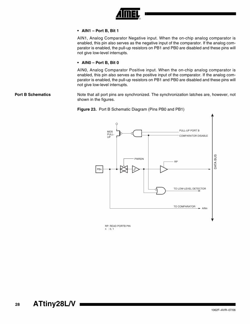
• AIN1 – Port B, Bit 1
AIN1, Analog Comparator Negative input. When the on-chip analog comparator isenabled, this pin also serves as the negative input of the comparator. If the analog com-parator is enabled, the pull-up resistors on PB1 and PB0 are disabled and these pins willnot give low-level interrupts.
• AIN0 – Port B, Bit 0
AIN0, Analog Comparator Positive input. When the on-chip analog comparator isenabled, this pin also serves as the positive input of the comparator. If the analog com-parator is enabled, the pull-up resistors on PB1 and PB0 are disabled and these pins willnot give low-level interrupts.
Port B Schematics Note that all port pins are synchronized. The synchronization latches are, however, notshown in the figures.
Figure 23. Port B Schematic Diagram (Pins PB0 and PB1)
DA
TA B
US
MOSPULL-UP
PBn
RP: READ PORTB PINn : 0, 1
PULL-UP PORT B
COMPARATOR DISABLE
RP
TO LOW-LEVEL DETECTOR
TO COMPARATORAINn
PWRDN
28 ATtiny28L/V 1062F–AVR–07/06
ATtiny28L/V
Figure 24. Port B Schematic Diagram (Pin PB2)
Figure 25. PORT B Schematic Diagram (Pins PB3 and PB4)
DA
TA B
US
MOSPULL-UP
PB2
RP: READ PORTB PIN
PULL-UP PORT B
RP
TO LOW-LEVEL DETECTOR
SENSE CONTROLTIMER0 CLOCKSOURCE MUX
CS02 CS01 CS00
DA
TA B
US
MOSPULL-UP
PBn
RP: READ PORTB PINn : 3, 4m : 0, 1
PULL-UP PORT B
RP
TO LOW-LEVEL DETECTOR
SENSE CONTROL INTm
ISCm1 ISCm0
INTm ENABLE
291062F–AVR–07/06

Figure 26. PORT B Schematic Diagram (Pins PB7 - PB5)
Port D Port D is an 8-bit bi-directional I/O port with internal pull-up resistors.
Three I/O memory address locations are allocated for Port D, one each for the DataRegister – PORTD, $12, Data Direction Register – DDRD, $11 and the Port D Input Pins– PIND, $10. The Port D Input Pins address is read-only, while the Data Register andthe Data Direction Register are read/write.
The Port D output buffers can sink 10 mA. As inputs, Port D pins that are externallypulled low will source current if the pull-up resistors are activated.
Port D as General Digital I/O All eight pins in Port D have equal functionality when used as digital I/O pins.
PDn, general I/O pin: The DDDn bit in the DDRD register selects the direction of this pin.If DDDn is set (one), PDn is configured as an output pin. If DDDn is cleared (zero), PDnis configured as an input pin. If PDn is set (one) when configured as an input pin, theMOS pull-up resistor is activated. To switch the pull-up resistor off, the PDn has to becleared (zero), or the pin has to be configured as an output pin. The port pins are tri-stated when a reset condition becomes active, even if the clock is not running.
Note: n: 7,6,...,0, pin number
DA
TA B
USPBn
TO LOW-LEVEL DETECTOR
RP:n:
READ PORT B PIN5 - 7
RP
MOSPULL-UP
PULL-UP PORT B
Table 12. DDDn Bits on Port D Pins
DDDn PORTDn I/O Pull-up Comment
0 0 Input No Tri-state (high-Z)
0 1 Input Yes PDn will source current if ext. pulled low
1 0 Output No Push-pull Zero Output
1 1 Output NO Push-pull One Output
30 ATtiny28L/V 1062F–AVR–07/06

ATtiny28L/V
Figure 27. Port D Schematic Diagram (Pins PD7 - PD0)
DA
TA B
US
D
D
Q
Q
RESET
RESET
C
C
WD
WP
RD
MOSPULL-UP
PDn
R
R
WP:WD:RL:RP:RD:
WRITE PORTDWRITE DDRDREAD PORTD LATCHREAD PORTD PINREAD DDRD
DDDn
PORTDn
RL
RP
n : 0 - 7
311062F–AVR–07/06

Register Description
Port A Data Register – PORTA
Port A Control Register – PACR
• Bits 7..4 – Res: Reserved Bits
These bits are reserved bits in the ATtiny28 and always read as zero.
• Bit 3 – DDA3: Data Direction PA3
When DDA3 is set (one), the corresponding pin is an output pin. Otherwise, it is an inputpin.
• Bit 2 – PA2HC: PORTA2 High Current Enable
When the PA2HC bit is set (one), an additional driver at the output pin PA2 is enabled.This makes it possible to sink 25 mA at VCC = 1.8V (VOL = 0.8V). When the PA2HC bit iscleared (zero), PA2 can sink 15 mA at VCC = 1.8V (VOL = 0.8V).
• Bits 1, 0 – DDA1, DDA0: Data Direction PA1 and PA0
When DDAn is set (one), the corresponding pin is an output pin. Otherwise, it is an inputpin.
Port A Input Pins Address – PINA
The Port A Input Pins address (PINA) is not a register; this address enables access tothe physical value on each Port A pin. When reading PORTA, the Port A Data Latch isread and when reading PINA, the logical values present on the pins are read.
Port B Input Pins Address – PINB
The Port B Input Pins address (PINB) is not a register; this address enables access tothe physical value on each Port B pin. When reading PINB, the logical values present onthe pins are read.
Bit 7 6 5 4 3 2 1 0
$1B – – – – PORTA3 PORTA2 PORTA1 PORTA0 PORTA
Read/Write R R R R R/W R/W R/W R/W
Initial Value 0 0 0 0 0 1 0 0
Bit 7 6 5 4 3 2 1 0
$1A – – – – DDA3 PA2HC DDA1 DDA0 PACR
Read/Write R R R R R/W R/W R/W R/W
Initial Value 0 0 0 0 0 0 0 0
Bit 7 6 5 4 3 2 1 0
$19 – – – – PINA3 – PINA1 PINA0 PINA
Read/Write R R R R R R R R
Initial Value 0 0 0 0 N/A 0 N/A N/A
Bit 7 6 5 4 3 2 1 0
$16 PINB7 PINB6 PINB5 PINB4 PINB3 PINB2 PINB1 PINB0 PINB
Read/Write R R R R R R R R
Initial Value N/A N/A N/A N/A N/A N/A N/A N/A
32 ATtiny28L/V 1062F–AVR–07/06
ATtiny28L/V
Port D Data Register – PORTD
Port D Data Direction Register – DDRD
Port D Input Pins Address – PIND
The Port D Input Pins Address (PIND) is not a register; this address enables access tothe physical value on each Port D pin. When reading PORTD, the Port D Data Latch isread and when reading PIND, the logical values present on the pins are read.
Bit 7 6 5 4 3 2 1 0
$12 PORTD7 PORTD6 PORTD5 PORTD4 PORTD3 PORTD2 PORTD1 PORTD0 PORTD
Read/Write R/W R/W R/W R/W R/W R/W R/W R/W
Initial Value 0 0 0 0 0 0 0 0
Bit 7 6 5 4 3 2 1 0
$11 DDD7 DDD6 DDD5 DDD4 DDD3 DDD2 DDD1 DDD0 DDRD
Read/Write R/W R/W R/W R/W R/W R/W R/W R/W
Initial Value 0 0 0 0 0 0 0 0
Bit 7 6 5 4 3 2 1 0
$10 PIND7 PIND6 PIND5 PIND4 PIND3 PIND2 PIND1 PIND0 PIND
Read/Write R R R R R R R R
Initial Value N/A N/A N/A N/A N/A N/A N/A N/A
331062F–AVR–07/06

Timer/Counter0 The ATtiny28 provides one general-purpose 8-bit Timer/Counter – Timer/Counter0.Timer/Counter0 has prescaling selection from the 10-bit prescaling timer. TheTimer/Counter0 can either be used as a timer with an internal clock time base or as acounter with an external pin connection that triggers the counting.
Timer/Counter Prescaler Figure 28 shows the Timer/Counter prescaler.
Figure 28. Timer/Counter0 Prescaler
The four different prescaled selections are: the hardware modulator period, CK/64,CK/256 and CK/1028, where CK is the oscillator clock. CK, external source and stopcan also be selected as clock sources.
Figure 29 shows the block diagram for Timer/Counter0.
Figure 29. Timer/Counter0 Block Diagram
10-BIT T/C PRESCALER
0
TIMER/COUNTER0 CLOCK SOURCETCK0
CK
T0
CS00CS01CS02
CK
/256
CK
/102
4
CK
/64
COUNT ENABLEFROM MODULATOR
T/C0 OVER-FLOW IRQ
INTERRUPT FLAGREGISTER (IFR)
T/C0 CONTROLREGISTER (TCCR0)
TIMER/COUNTER0(TCNT0)
CONTROLLOGIC
TOV
0
INTERRUPT CONTROLREGISTER (ICR)
TOIE
0
TOV
0
T0
34 ATtiny28L/V 1062F–AVR–07/06
ATtiny28L/V
The 8-bit Timer/Counter0 can select clock source from CK, prescaled CK or an externalpin. In addit ion, it can be stopped as described in the specif ication for theTimer/Counter0 Control Register (TCCR0). The overflow status flag is found in the Inter-rupt Flag Register (IFR). Control signals are found in the Timer/Counter0 ControlRegister (TCCR0). The interrupt enable/disable setting for Timer/Counter0 is found inthe Interrupt Control Register (ICR).
When Timer/Counter0 is externally clocked, the external signal is synchronized with theoscillator frequency of the CPU. To ensure proper sampling of the external clock, theminimum time between two external clock transitions must be at least one internal CPUclock period. The external clock signal is sampled on the rising edge of the internal CPUclock.
The 8-bit Timer/Counter0 features both a high-resolution and a high-accuracy usagewith the lower prescaling opportunities. Similarly, the high prescaling opportunities makethe Timer/Counter0 useful for lower speed functions or exact timing functions with infre-quent actions.
Register Description
Timer/Counter0 Control Register – TCCR0
• Bit 7 – FOV0: Force Overflow
Writing a logical “1” to this bit forces a change on the overflow output pin PA2 accordingto the values already set in OOM01 and OOM00. If the OOM01 and OOM00 bits arewritten in the same cycle as FOV0, the new settings will not take effect until the nextoverflow or forced overflow occurs. The Force Overflow bit can be used to change theoutput pin without waiting for an overflow in the timer. The automatic action programmedin OOM01 and OOM00 happens as if an overflow had occurred, but no interrupt is gen-erated. The FOV0 bit will always read as zero, and writing a zero to this bit has no effect.
• Bits 6, 5 – Res: Reserved Bits
These bits are reserved bits in the ATtiny28 and always read as zero.
• Bits 4, 3 – OOM01, OOM00: Overflow Output Mode, Bits 1 and 0
The OOM01 and OOM00 control bits determine any output pin action following an over-flow or a forced overflow in Timer/Counter0. Any output pin actions affect pin PA2. Thecontrol configuration is shown in Table 13.
Bit 7 6 5 4 3 2 1 0
$04 FOV0 – – OOM01 OOM00 CS02 CS01 CS00 TCCR0
Read/Write R/W R R R/W R/W R/W R/W R/W
Initial Value 0 0 0 0 0 0 0 0
Table 13. Overflow Output Mode Select
OOM01 OOM00 Description
0 0 Timer/Counter0 disconnected from output pin PA2
0 1 Toggle the PA2 output line.
1 0 Clear the PA2 output line to zero.
1 1 Set the PA2 output line to one.
351062F–AVR–07/06

• Bits 2, 1, 0 – CS02, CS01, CS00: Clock Select0, Bits 2, 1 and 0
The Clock Select0 bits 2, 1 and 0 define the prescaling source of Timer/Counter0.
The Stop condition provides a Timer Enable/Disable function. The CK down dividedmodes are scaled directly from the CK oscillator clock. If the external pin modes areused for Timer/Counter0, transitions on PB2/(T0) will clock the counter even if the pin isconfigured as an output. This feature can give the user software control of the counting.
Timer Counter 0 – TCNT0
The Timer/Counter0 is realized as an up-counter with read and write access. If theTimer/Counter0 is written and a clock source is present, the Timer/Counter0 continuescounting in the timer clock cycle following the write operation.
Table 14. Clock 0 Prescale Select
CS02 CS01 CS00 Description
0 0 0 Stop, the Timer/Counter0 is stopped.
0 0 1 CK
0 1 0 Modulator Period
0 1 1 CK/64
1 0 0 CK/256
1 0 1 CK/1024
1 1 0 External Pin T0, falling edge
1 1 1 External Pin T0, rising edge
Bit 7 6 5 4 3 2 1 0
$03 MSB LSB TCNT0
Read/Write R/W R/W R/W R/W R/W R/W R/W R/W
Initial Value 0 0 0 0 0 0 0 0
36 ATtiny28L/V 1062F–AVR–07/06

ATtiny28L/V
Watchdog Timer The Watchdog Timer is clocked from a separate on-chip oscillator. By controlling theWatchdog Timer prescaler, the Watchdog reset interval can be adjusted as shown inTable 15. See characterization data for typical values at other VCC levels. The WDR(Watchdog Reset) instruction resets the Watchdog Timer. Eight different clock cycleperiods can be selected to determine the reset period. If the reset period expires withoutanother Watchdog reset, the ATtiny28 resets and executes from the reset vector. Fortiming details on the Watchdog reset, refer to page 18.
To prevent unintentional disabling of the Watchdog, a special turn-off sequence must befollowed when the Watchdog is disabled. Refer to the description of the Watchdog TimerControl Register for details.
Figure 30. Watchdog Timer
Register Description
Watchdog Timer Control Register – WDTCR
• Bits 7..5 - Res: Reserved Bits
These bits are reserved bits in the ATtiny28 and will always read as zero.
• Bit 4 – WDTOE: Watchdog Turn-off Enable
This bit must be set (one) when the WDE bit is cleared. Otherwise, the Watchdog willnot be disabled. Once set, hardware will clear this bit to zero after four clock cycles.Refer to the description of the WDE bit for a Watchdog disable procedure.
• Bit 3 – WDE: Watchdog Enable
When the WDE is set (one), the Watchdog Timer is enabled and if the WDE is cleared(zero), the Watchdog Timer function is disabled. WDE can only be cleared if theWDTOE bit is set (one). To disable an enabled Watchdog Timer, the following proce-dure must be followed:
1 MHz at VCC = 5V
350 kHz at VCC = 3V
110 kHz at VCC = 2V
Oscillator
Bit 7 6 5 4 3 2 1 0
$01 – – – WDTOE WDE WDP2 WDP1 WDP0 WDTCR
Read/Write R R R R/W R/W R/W R/W R/W
Initial Value 0 0 0 0 0 0 0 0
371062F–AVR–07/06

1. In the same operation, write a logical “1” to WDTOE and WDE. A logical “1” must be written to WDE even though it is set to one before the disable operation starts.
2. Within the next four clock cycles, write a logical “0” to WDE. This disables the Watchdog.
• Bits 2..0 – WDP2, WDP1, WDP0: Watchdog Timer Prescaler 2, 1 and 0
The WDP2, WDP1 and WDP0 bits determine the Watchdog Timer prescaling when theWatchdog Timer is enabled. The different prescaling values and their correspondingtime-out periods are shown in Table 15.
Note: The frequency of the Watchdog oscillator is voltage-dependent, as shown in the section“Typical Characteristics” on page 57.The WDR (Watchdog Reset) instruction should always be executed before the WatchdogTimer is enabled. This ensures that the reset period will be in accordance with theWatchdog Timer prescale settings. If the Watchdog Timer is enabled without reset, theWatchdog Timer may not start counting from zero.
Table 15. Watchdog Timer Prescale Select
WDP2 WDP1 WDP0
Number of WDT Oscillator Cycles
Typical Time-out at VCC = 2.0V
Typical Time-out at VCC = 3.0V
Typical Time-out at VCC = 5.0V
0 0 0 16K cycles 0.15 s 47 ms 15 ms
0 0 1 32K cycles 0.30 s 94 ms 30 ms
0 1 0 64K cycles 0.60 s 0.19 s 60 ms
0 1 1 128K cycles 1.2 s 0.38 s 0.12 s
1 0 0 256K cycles 2.4 s 0.75 s 0.24 s
1 0 1 512K cycles 4.8 s 1.5 s 0.49 s
1 1 0 1,024K cycles 9.6 s 3.0 s 0.97 s
1 1 1 2,048K cycles 19 s 6.0 s 1.9 s
38 ATtiny28L/V 1062F–AVR–07/06

ATtiny28L/V
Hardware Modulator ATtiny28 features a built-in hardware modulator connected to a high-current output pad,PA2. The hardware modulator generates a configurable pulse train. The on-time of apulse can be set to a number of chip clock cycles. This is done by configuring the Modu-lation Control Register (MODCR).
PA2 is the built-in, high-current LED driver and it is always an output pin. The outputbuffer can sink 25 mA at VCC = 2.0V. When MCONF is zero, modulation is switched offand the pin acts as a normal high-current output pin. The following truth table shows theeffect of various PORTA2 and MCONF settings.
The modulation period is available as a prescale to Timer/Counter0 and thus, this timershould be used to time the length of each burst. If the number of pulses to be sent is N,the number 255 - N should be loaded to the timer. When an overflow occurs, the trans-mission is complete.The OOM01 and OOM00 bits in TCCR0 can be configured toautomatically change the value on PA2 when a Timer/Counter0 overflow occurs. See“Timer/Counter0” on page 34 for details on how to configure the OOM01 and OOM00bits.
The modulation period is available as a prescale even when PORTA2 is high and mod-ulation is stopped. Thus, this prescale can also be used to time the intervals betweenbursts.
To get a glitch-free output, the user should first configure the MODCR register to enablemodulation. There are two ways to start the modulation:
1. Clear the PORTA2 bit in Port A Data Register (PORTA).
2. Configure OOM00 and OOM01 bits in the Timer/Counter0 Control Register (TCCR0) to clear PA2 on the next overflow. Either an overflow or a forced over-flow can then be used to start modulation.
The PA2 output will then be set low at the start of the next cycle. To stop the modulatedoutput, the user should set the PORTA2 bit or configure OOM00 and OOM01 to set PA2on the next overflow. If the MODCR register is changed during modulation, the changedvalue will take effect at the start of the next cycle, producing a glitch-free output. SeeFigure 31 below and Figure 22 on page 26.
Table 16. PA2 Output
PORTA2 MCONF PA2 Output
0 0 0
0 1 - 7 Modulated
1 X 1
391062F–AVR–07/06

Figure 31. The Hardware Modulator
Figure 32 to Figure 35 show examples on output from the Modulator. Figure 32 alsoshows the timing for the enable setting signal and for the count enable signal toTimer/Counter0.
Figure 32. Modulation with ONTIM = 3, MCONF = 010.
Note: 1. Clock frequency: 455 kHz; modulation frequency: 38 kHz; duty-cycle: 33%
Figure 33. Modulation with ONTIM = 5, MCONF = 001
Note: Clock frequency: 455 kHz; modulation frequency: 38 kHz; duty-cycle: 50%
DISABLEMODUALTOR
PA201D Q
IPO
RT
A2FROM
PORTA2
ENABLE SETTING
MODULATORSTATE
MACHINE
COUNT ENABLETO TIMER/COUNTER0
ION
TIM
IMC
ON
F
5
ON
TIM
MC
ON
F
3
RM
WM
8
5
3
5
3
/
/
/
/
/
/
/
WM: WRITE MODCRRM: READ MODCR
CLK
PA2
COUNTENABLE
ENABLESETTING
CLK
PA2
40 ATtiny28L/V 1062F–AVR–07/06

ATtiny28L/V
Figure 34. Modulation with ONTIM = 1, MCONF = 011
Note: Clock frequency: 3.64 MHz; modulation frequency: 455 kHz; duty-cycle: 25%
Figure 35. Modulation with ONTIM = 3, MCONF = 001
Note: Clock frequency: 3.64 MHz; modulation frequency: 455 kHz; duty-cycle: 50%
Table 17. Some Common Modulator Configurations
Crystal/Resonator Frequency
Carrier Frequency
% Error in Frequency Duty-cycle
ONTIM Value
MCONF Value
455 kHz 38 kHz 0.2 25% 2 011
455 kHz 38 kHz 0.2 33% 3 010
455 kHz 38 kHz 0.2 50% 5 001
455 kHz 38 kHz 0.2 67% 3 100
455 kHz 38 kHz 0.2 75% 2 101
1 MHz 38 kHz 1.2 50% 12 001
1.8432 MHz 38 kHz 1.1 25% 11 011
1.8432 MHz 38 kHz 1.1 33% 15 010
1.8432 MHz 38 kHz 1.1 50% 23 001
2 MHz 38 kHz 1.2 25% 12 011
2 MHz 38 kHz 1.2 50% 25 001
2.4576 MHz 38 kHz 1.1 50% 31 001
3.2768 MHz 38 kHz 2.0 25% 21 011
4 MHz 38 kHz 1.2 25% 25 011
455 kHz 455 kHz 0.0 approx. 50% X 111
1 MHz 455 kHz 9.9 50% 0 001
1.82 MHz 455 kHz 0.0 25% 0 011
1.82 MHz 455 kHz 0.0 50% 1 001
1.8432 MHz 455 kHz 1.3 25% 0 011
1.8432 MHz 455 kHz 1.3 50% 1 001
2 MHz 455 kHz 9.9 25% 0 011
CLK
PA2
CLK
PA2
411062F–AVR–07/06

2 MHz 455 kHz 9.9 50% 1 001
2.4576 MHz 455 kHz 10.0 33% 1 010
2.4576 MHz 455 kHz 10.0 50% 2 001
3.2768 MHz 455 kHz 10.0 25% 1 011
3.2768 MHz 455 kHz 10.0 50% 3 001
3.64 MHz 455 kHz 0.0 25% 1 011
3.64 MHz 455 kHz 0.0 50% 3 001
4 MHz 455 kHz 9.9 25% 1 011
4 MHz 455 kHz 9.9 50% 3 001
Table 17. Some Common Modulator Configurations (Continued)
Crystal/Resonator Frequency
Carrier Frequency
% Error in Frequency Duty-cycle
ONTIM Value
MCONF Value
42 ATtiny28L/V 1062F–AVR–07/06

ATtiny28L/V
Register Description
Modulation Control Register – MODCR
• Bits 7..3 – ONTIM4..0: Modulation On-time
This 5-bit value +1 determines the number of clock cycles the output pin PA2 is active(low).
• Bits 2..0 – MCONF2..0: Modulation Configuration Bits 2, 1 and 0
These three bits determine the relationship between the on- and off-times of the modu-lator, and thereby the duty-cycle. The various settings are shown in Table 18. Theminimum and maximum modulation period is also shown in the table. The minimummodulation period is obtained by setting ONTIM to zero, while the maximum period isobtained by setting ONTIM to 31. The configuration values for some common oscillatorand carrier frequencies are listed in Table 17. The relationship between oscillator fre-quency and carrier frequency is:
If the MCONF register is set to 111, the carrier frequency will be equal to the oscillatorfrequency.
Note: In the high-frequency mode, the output is gated with the clock signal. Thus, the on- and off-times will be dependent on the clockinput to the MCU. Also note that when changing from this mode directly to another modulation mode, the output will have asmall glitch. Thus, PA2 should be set to stop the modulated output before changing from this mode.
Bit 7 6 5 4 3 2 1 0
$02 ONTIM4 ONTIM3 ONTIM2 ONTIM1 ONTIM0 MCONF2 MCONF1 MCONF0 MODCR
Read/Write R/W R/W R/W R/W R/W R/W R/W R/W
Initial Value 0 0 0 0 0 0 0 0
fcarrier foscOn-time Off-time+( )
-----------------------------------------------------=
Table 18. MCONF2..0 Effect on Duty-cycle and Modulation Period
MCONF2..0 On-time Off-time Duty-cycle Min Period Max Period Comment
000 X X 100% X X Unmodulated output
001 ONTIM+1 ONTIM+1 50% 2 CK 64 CK
010 ONTIM+1 2 x (ONTIM+1) 33% 3 CK 96 CK
011 ONTIM+1 3 x (ONTIM+1) 25% 4 CK 128 CK
100 2 x (ONTIM+1) ONTIM+1 67% 3 CK 96 CK
101 3 x (ONTIM+1) ONTIM+1 75% 4 CK 128 CK
110 Reserved
111 X X Note 1 1 CK 1 CK High-frequency output
431062F–AVR–07/06

Analog Comparator The analog comparator compares the input values on the positive input PB0 (AIN0) andnegative input PB1 (AIN1). When the voltage on the positive input PB0 (AIN0) is higherthan the voltage on the negative input PB1 (AIN1), the Analog Comparator Output(ACO) is set (one). The comparator can trigger a separate interrupt exclusive to the ana-log comparator. The user can select interrupt triggering on comparator output rise, fall ortoggle. A block diagram of the comparator and its surrounding logic is shown in Figure36.
Figure 36. Analog Comparator Block Diagram
Register Description
Analog Comparator Control and Status Register – ACSR
• Bit 7 – ACD: Analog Comparator Disable
When this bit is set (one), the power to the analog comparator is switched off. This bitcan be set at any time to turn off the analog comparator. When changing the ACD bit,the Analog Comparator Interrupt must be disabled by clearing the ACIE bit in ACSR.Otherwise, an interrupt can occur when the bit is changed. To use the analog compara-tor, the user must clear this bit.
• Bit 6 – Res: Reserved Bit
This bit is a reserved bit in the ATtiny28 and will always read as zero.
• Bit 5 – ACO: Analog Comparator Output
ACO is directly connected to the comparator output.
• Bit 4 – ACI: Analog Comparator Interrupt Flag
This bit is set (one) when a comparator output event triggers the interrupt mode definedby ACI1 and ACI0. The Analog Comparator Interrupt routine is executed if the ACIE bitis set (one) and the I-bit in SREG is set (one). ACI is cleared by hardware when execut-
PB0
PB1
Bit 7 6 5 4 3 2 1 0
$08 ACD – ACO ACI ACIE – ACIS1 ACIS0 ACSR
Read/Write R/W R R R/W R/W R R/W R/W
Initial Value 1 0 X 0 0 0 0 0
44 ATtiny28L/V 1062F–AVR–07/06

ATtiny28L/V
ing the corresponding interrupt handling vector. Alternatively, ACI is cleared by writing alogical “1” to the flag.
• Bit 3 – ACIE: Analog Comparator Interrupt Enable
When the ACIE bit is set (one) and the I-bit in the Status Register is set (one), the ana-log comparator interrupt is activated. When cleared (zero), the interrupt is disabled.
• Bit 2 – RES: Reserved Bit
This bit is a reserved bit in the ATtiny28 and will always read as zero.
• Bits 1, 0 - ACIS1, ACIS0: Analog Comparator Interrupt Mode Select
These bits determine which comparator events trigger the Analog Comparator Interrupt.The different settings are shown in Table 19.
Note: When changing the ACIS1/ACIS0 bits, the Analog Comparator Interrupt must be dis-abled by clearing its Interrupt Enable bit in the ACSR register. Otherwise, an interrupt canoccur when the bits are changed.
Caution: Using the SBI or CBI instruction on bits other than ACI in this register will writea one back into ACI if it is read as set, thus clearing the flag.
Table 19. ACIS1/ACIS0 Settings
ACIS1 ACIS0 Interrupt Mode
0 0 Comparator Interrupt on Output Toggle
0 1 Reserved
1 0 Comparator Interrupt on Falling Output Edge
1 1 Comparator Interrupt on Rising Output Edge
451062F–AVR–07/06

Memory Programming
Program Memory Lock Bits
The ATtiny28 MCU provides two Lock bits that can be left unprogrammed (“1”) or can beprogrammed (“0”) to obtain the additional features listed in Table 20. The Lock bits canonly be erased with the Chip Erase command.
Note: 1. Further programming of the Fuse bits is also disabled. Program the Fuse bits beforeprogramming the Lock bits.
Fuse Bits The ATtiny28 has five Fuse bits, INTCAP and CKSEL3..0.
• When the INTCAP Fuse is programmed (“0”), internal load capacitors are connected between XTAL1/XTAL2 and GND, similar to C1 and C2 in Figure 5. See “Crystal Oscillator” on page 7. Default value is unprogrammed (“1”).
• CKSEL3..0 Fuses: See Table 1, “Device Clocking Option Select,” on page 7 and Table 5, “ATtiny28 Clock Options and Start-up Time,” on page 16, for which combination of CKSEL3..0 to use. Default value is “0010”, internal RC oscillator with long start-up time.
The status of the Fuse bits is not affected by Chip Erase.
Signature Bytes All Atmel microcontrollers have a 3-byte signature code that identifies the device. Thethree bytes reside in a separate address space.
For the ATtiny28, they are:
1. $000: $1E (indicates manufactured by Atmel)
2. $001: $91 (indicates 2 KB Flash memory)
3. $002: $07 (indicates ATtiny28 device when signature byte $001 is $91)
Calibration Byte The ATtiny28 has one byte calibration value for the internal RC oscillator. This byteresides in the high byte of address $000 in the signature address space. During memoryprogramming, the external programmer must read this location, and program it into aselected location in the the normal Flash program memory. At start-up, the user soft-ware must read this Flash location and write the value to the OSCCAL register.
Table 20. Lock Bit Protection Modes
Memory Lock Bits
Protection TypeMode LB1 LB2
1 1 1 No memory lock features enabled.
2 0 1 Further programming of the Flash is disabled.(1)
3 0 0 Same as mode 2, and verify is also disabled.
46 ATtiny28L/V 1062F–AVR–07/06
ATtiny28L/V
Programming the Flash Atmel’s ATtiny28 offers 2K bytes of Flash program memory.
The ATtiny28 is shipped with the on-chip Flash program memory array in the erasedstate (i.e., contents = $FF) and ready to be programmed. This device supports a high-voltage (12V) parallel programming mode. Only minor currents (<1mA) are drawn fromthe +12V pin during programming.
The program memory array in the ATtiny28 is programmed byte-by-byte. During pro-gramming, the supply voltage must be in accordance with Table 21.
Parallel Programming This section describes how to parallel program and verify Flash program memory, Lockbits and Fuse bits in the ATtiny28.
Signal Names In this section, some pins of the ATtiny28 are referenced by signal names describingtheir function during parallel programming. See Figure 37 and Table 22. Pins notdescribed in Table 22 are referenced by pin name.
The XA1/XA0 pins determine the action executed when the XTAL1 pin is given a posi-tive pulse. The coding is shown in Table 23.
When pulsing WR or OE, the command loaded determines the action executed. Thecommand is a byte where the different bits are assigned functions, as shown in Table24.
Figure 37. Parallel Programming
Table 21. Supply Voltage during Programming
Part Serial Programming Parallel Programming
ATtiny28 Not applicable 4.5 - 5.5V
VCC
+5V
RESET
GND
XTAL1
PD1
PD2
PD3
PD4
PD5
PD6
+12V
RDY/BSY
OE
BS
XA0
XA1
WR
PB7 - PB0 DATA
ATtiny28
471062F–AVR–07/06
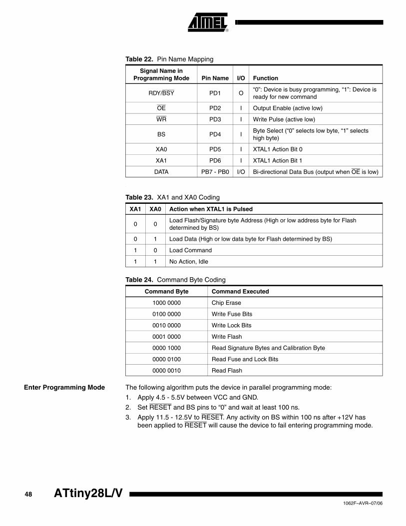
.
Enter Programming Mode The following algorithm puts the device in parallel programming mode:
1. Apply 4.5 - 5.5V between VCC and GND.
2. Set RESET and BS pins to “0” and wait at least 100 ns.
3. Apply 11.5 - 12.5V to RESET. Any activity on BS within 100 ns after +12V has been applied to RESET will cause the device to fail entering programming mode.
Table 22. Pin Name Mapping
Signal Name in Programming Mode Pin Name I/O Function
RDY/BSY PD1 O“0”: Device is busy programming, “1”: Device is ready for new command
OE PD2 I Output Enable (active low)
WR PD3 I Write Pulse (active low)
BS PD4 IByte Select (“0” selects low byte, “1” selects high byte)
XA0 PD5 I XTAL1 Action Bit 0
XA1 PD6 I XTAL1 Action Bit 1
DATA PB7 - PB0 I/O Bi-directional Data Bus (output when OE is low)
Table 23. XA1 and XA0 Coding
XA1 XA0 Action when XTAL1 is Pulsed
0 0Load Flash/Signature byte Address (High or low address byte for Flash determined by BS)
0 1 Load Data (High or low data byte for Flash determined by BS)
1 0 Load Command
1 1 No Action, Idle
Table 24. Command Byte Coding
Command Byte Command Executed
1000 0000 Chip Erase
0100 0000 Write Fuse Bits
0010 0000 Write Lock Bits
0001 0000 Write Flash
0000 1000 Read Signature Bytes and Calibration Byte
0000 0100 Read Fuse and Lock Bits
0000 0010 Read Flash
48 ATtiny28L/V 1062F–AVR–07/06

ATtiny28L/V
Chip Erase The Chip Erase command will erase the Flash memory and the Lock bits. The Lock bitsare not reset until the Flash has been completely erased. The Fuse bits are notchanged. Chip Erase must be performed before the Flash is reprogrammed.
Load Command “Chip Erase”
1. Set XA1, XA0 to “10”. This enables command loading.
2. Set BS to “0”.
3. Set DATA to “1000 0000”. This is the command for Chip Erase.
4. Give XTAL1 a positive pulse. This loads the command.
5. Give WR a negative pulse. This starts the Chip Erase. RDY/BSY goes low.
6. Wait until RDY/BSY goes high before loading a new command.
Programming the Flash A: Load Command “Write Flash”
1. Set XA1, XA0 to “10”. This enables command loading.
2. Set BS to “0”.
3. Set DATA to “0001 0000”. This is the command for Write Flash.
4. Give XTAL1 a positive pulse. This loads the command.
B: Load Address High Byte
1. Set XA1, XA0 to “00”. This enables address loading.
2. Set BS to “1”. This selects high byte.
3. Set DATA = Address high byte ($00 - $03).
4. Give XTAL1 a positive pulse. This loads the address high byte.
C: Load Address Low Byte
1. Set XA1, XA0 to “00”. This enables address loading.
2. Set BS to “0”. This selects low byte.
3. Set DATA = Address low byte ($00 - $FF).
4. Give XTAL1 a positive pulse. This loads the address low byte.
D: Load Data Low Byte
1. Set XA1, XA0 to “01”. This enables data loading.
2. Set DATA = Data low byte ($00 - $FF).
3. Give XTAL1 a positive pulse. This loads the data low byte.
E: Write Data Low Byte
1. Set BS to “0”. This selects low data.
2. Give WR a negative pulse. This starts programming of the data byte. RDY/BSY goes low.
3. Wait until RDY/BSY goes high to program the next byte.
(See Figure 38 for signal waveforms.)
F: Load Data High Byte
1. Set XA1, XA0 to “01”. This enables data loading.
2. Set DATA = Data high byte ($00 - $FF).
3. Give XTAL1 a positive pulse. This loads the data high byte.
G: Write Data High Byte
491062F–AVR–07/06

1. Set BS to “1”. This selects high data.
2. Give WR a negative pulse. This starts programming of the data byte. RDY/BSY goes low.
3. Wait until RDY/BSY goes high to program the next byte.
(See Figure 39 for signal waveforms.)
The loaded command and address are retained in the device during programming. Forefficient programming, the following should be considered:
• The command needs to be loaded only once when writing or reading multiple memory locations.
• Address high byte only needs to be loaded before programming a new 256-word page in the Flash.
• Skip writing the data value $FF, that is, the contents of the entire Flash after a Chip Erase.
These considerations also apply to Flash and signature bytes reading.
Reading the Flash The algorithm for reading the Flash memory is as follows (refer to “Programming theFlash” for details on command and address loading):
A: Load Command “0000 0010”.
B: Load Address High Byte ($00 - $03).
C: Load Address Low Byte ($00 - $FF).
1. Set OE to “0”, and BS to “0”. The Flash word low byte can now be read at DATA.
2. Set BS to “1”. The Flash word high byte can now be read from DATA.
3. Set OE to “1”.
Programming the Fuse Bits The algorithm for programming the Fuse bits is as follows (refer to “Programming theFlash” for details on command and data loading):
A: Load Command “0100 0000”.
D: Load Data Low Byte. Bit n = “0” programs and bit n = “1” erases the Fuse bit.
Bit 4 = INTCAP FuseBit 3 = CKSEL3 FuseBit 2 = CKSEL2 FuseBit 1 = CKSEL1 FuseBit 0 = CKSEL0 FuseBits 7 - 5 = “1”. These bits are reserved and should be left unprogrammed (“1”).
E: Write Data Low Byte.
Programming the Lock Bits The algorithm for programming the Lock bits is as follows (refer to “Programming theFlash” for details on command and data loading):
A: Load Command “0010 0000”.
D: Load Data Low Byte. Bit n = “0” programs the Lock bit.
Bit 2 = Lock Bit2Bit 1 = Lock Bit1Bits 7 - 3,0 = “1”. These bits are reserved and should be left unprogrammed (“1”).
E: Write Data Low Byte.
The Lock bits can only be cleared by executing Chip Erase.
50 ATtiny28L/V 1062F–AVR–07/06

ATtiny28L/V
Reading the Fuse and Lock Bits
The algorithm for reading the Fuse and Lock bits is as follows (refer to “Programmingthe Flash” for details on command loading):
A: Load Command “0000 0100”.
1. Set OE to “0”, and BS to “0”. The status of the Fuse bits can now be read at DATA (“0” means programmed).Bit 4 = INTCAP FuseBit 3 = CKSEL3 FuseBit 2 = CKSEL2 FuseBit 1 = CKSEL1 FuseBit 0 = CKSEL0 Fuse
2. Set BS to “1”. The status of the Lock bits can now be read at DATA (“0” means programmed).Bit 2: Lock Bit2Bit 1: Lock Bit1
3. Set OE to “1”.
Reading the Signature Bytes and Calibration Byte
The algorithm for reading the signature bytes and the calibration byte is as follows (referto “Programming the Flash” for details on command and address loading):
A: Load Command “0000 1000”.
C: Load Address Low Byte ($00 - $02).
1. Set OE to “0”, and BS to “0”. The selected signature byte can now be read at DATA.
C: Load Address Low Byte ($00).
1. Set OE to “0”, and BS to “1”. The calibration byte can now be read at DATA.
2. Set OE to “1”.
Figure 38. Programming the Flash Waveforms
$10 ADDR. HIGH ADDR. LOW DATA LOWDATA
XA1
XA0
BS
XTAL1
WR
RDY/BSY
RESET
OE
12V
511062F–AVR–07/06
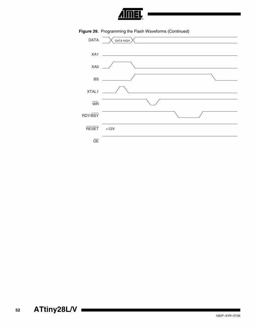
Figure 39. Programming the Flash Waveforms (Continued)
DATA HIGHDATA
XA1
XA0
BS
XTAL1
WR
RDY/BSY
RESET +12V
OE
52 ATtiny28L/V 1062F–AVR–07/06
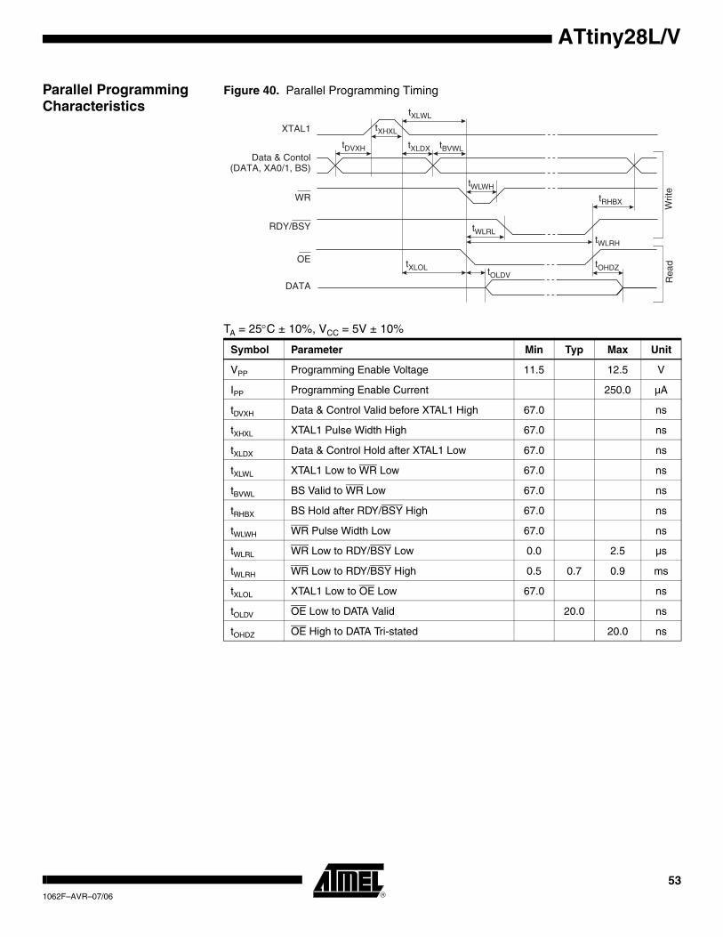
ATtiny28L/V
Parallel Programming Characteristics
Figure 40. Parallel Programming Timing
TA = 25°C ± 10%, VCC = 5V ± 10%
Symbol Parameter Min Typ Max Unit
VPP Programming Enable Voltage 11.5 12.5 V
IPP Programming Enable Current 250.0 µA
tDVXH Data & Control Valid before XTAL1 High 67.0 ns
tXHXL XTAL1 Pulse Width High 67.0 ns
tXLDX Data & Control Hold after XTAL1 Low 67.0 ns
tXLWL XTAL1 Low to WR Low 67.0 ns
tBVWL BS Valid to WR Low 67.0 ns
tRHBX BS Hold after RDY/BSY High 67.0 ns
tWLWH WR Pulse Width Low 67.0 ns
tWLRL WR Low to RDY/BSY Low 0.0 2.5 µs
tWLRH WR Low to RDY/BSY High 0.5 0.7 0.9 ms
tXLOL XTAL1 Low to OE Low 67.0 ns
tOLDV OE Low to DATA Valid 20.0 ns
tOHDZ OE High to DATA Tri-stated 20.0 ns
Data & Contol(DATA, XA0/1, BS)
DATA
Writ
eR
ead
XTAL1 tXHXL
tWLWH
tDVXH
tXLOL tOLDV
tWLRLtWLRH
WR
RDY/BSY
OE
tXLDX
tXLWL
tRHBX
tOHDZ
tBVWL
531062F–AVR–07/06
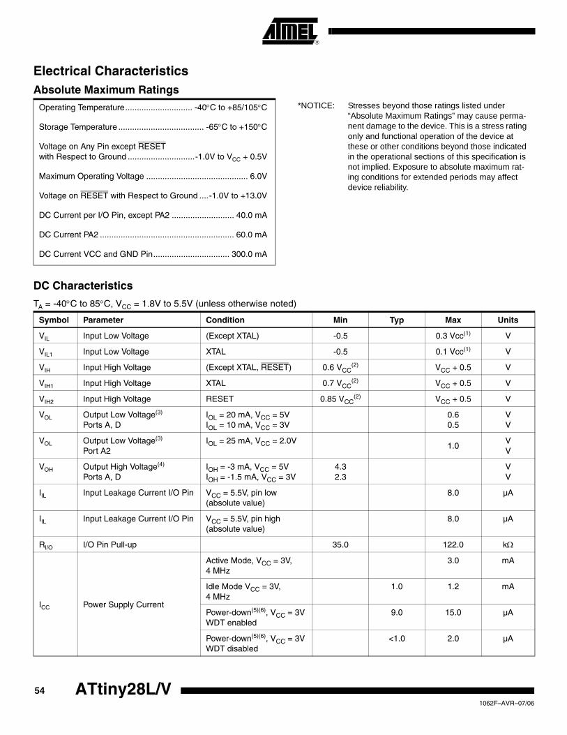
Electrical CharacteristicsAbsolute Maximum Ratings
Operating Temperature............................. -40°C to +85/105°C *NOTICE: Stresses beyond those ratings listed under “Absolute Maximum Ratings” may cause perma-nent damage to the device. This is a stress rating only and functional operation of the device at these or other conditions beyond those indicated in the operational sections of this specification is not implied. Exposure to absolute maximum rat-ing conditions for extended periods may affect device reliability.
Storage Temperature ..................................... -65°C to +150°C
Voltage on Any Pin except RESETwith Respect to Ground .............................-1.0V to VCC + 0.5V
Maximum Operating Voltage ............................................ 6.0V
Voltage on RESET with Respect to Ground ....-1.0V to +13.0V
DC Current per I/O Pin, except PA2 ........................... 40.0 mA
DC Current PA2 .......................................................... 60.0 mA
DC Current VCC and GND Pin................................. 300.0 mA
DC Characteristics
TA = -40°C to 85°C, VCC = 1.8V to 5.5V (unless otherwise noted)
Symbol Parameter Condition Min Typ Max Units
VIL Input Low Voltage (Except XTAL) -0.5 0.3 Vcc(1) V
VIL1 Input Low Voltage XTAL -0.5 0.1 Vcc(1) V
VIH Input High Voltage (Except XTAL, RESET) 0.6 VCC(2) VCC + 0.5 V
VIH1 Input High Voltage XTAL 0.7 VCC(2) VCC + 0.5 V
VIH2 Input High Voltage RESET 0.85 VCC(2) VCC + 0.5 V
VOL Output Low Voltage(3)
Ports A, DIOL = 20 mA, VCC = 5VIOL = 10 mA, VCC = 3V
0.60.5
VV
VOL Output Low Voltage(3)
Port A2IOL = 25 mA, VCC = 2.0V
1.0VV
VOH Output High Voltage(4)
Ports A, DIOH = -3 mA, VCC = 5VIOH = -1.5 mA, VCC = 3V
4.32.3
VV
IIL Input Leakage Current I/O Pin VCC = 5.5V, pin low(absolute value)
8.0 µA
IIL Input Leakage Current I/O Pin VCC = 5.5V, pin high(absolute value)
8.0 µA
RI/O I/O Pin Pull-up 35.0 122.0 kΩ
ICC Power Supply Current
Active Mode, VCC = 3V, 4 MHz
3.0 mA
Idle Mode VCC = 3V, 4 MHz
1.0 1.2 mA
Power-down(5)(6), VCC = 3VWDT enabled
9.0 15.0 µA
Power-down(5)(6), VCC = 3VWDT disabled
<1.0 2.0 µA
54 ATtiny28L/V 1062F–AVR–07/06
ATtiny28L/V
Notes: 1. “Max” means the highest value where the pin is guaranteed to be read as low.2. “Min” means the lowest value where the pin is guaranteed to be read as high.3. Although each I/O port can sink more than the test conditions (20 mA at VCC = 5V, 10 mA at VCC = 3V) under steady-state
conditions (non-transient), the following must be observed:1] The sum of all IOL, for all ports, should not exceed 300 mA.2] The sum of all IOL, for port D0 - D7 and XTAL2 should not exceed 100 mA.If IOL exceeds the test condition, VOL may exceed the related specification.Pins are not guaranteed to sink current greater than the listed test conditions.
4. Although each I/O port can source more than the test conditions (3 mA at VCC = 5V, 1.5 mA at VCC = 3V) under steady-stateconditions (non-transient), the following must be observed:1] The sum of all IOH, for all ports, should not exceed 300 mA.2] The sum of all IOH, for port D0 - D7 and XTAL2 should not exceed 100 mA.If IOH exceeds the test condition, VOH may exceed the related specification.Pins are not guaranteed to source current greater than the listed test conditions.
5. Minimum VCC for power-down is 1.5V.6. When entering Power-down, PORTA2 bit in PORTA register should be set.
VACIO Analog Comparator Input Offset Voltage
VCC = 5VVIN = VCC/2
40.0 mV
IACLK Analog Comparator Input Leakage Current
VCC = 5VVIN = VCC/2
-50.0 50.0 nA
TACPD Analog Comparator Propagation Delay
VCC = 2.7VVCC = 4.0V
750.0
500.0
ns
DC Characteristics (Continued)
TA = -40°C to 85°C, VCC = 1.8V to 5.5V (unless otherwise noted)
Symbol Parameter Condition Min Typ Max Units
551062F–AVR–07/06

External Clock Drive Waveforms
Figure 41. External Clock
:
Note: R should be in the range 3 - 100 kΩ, and C should be at least 20 pF.
VIL1
VIH1
External Clock Drive
Symbol Parameter
VCC = 1.8V to 2.7V VCC = 2.7V to 4.0V VCC = 4.0V to 5.5V
UnitsMin Max Min Max Min Max
1/tCLCL Oscillator Frequency 0.0 1.2 0.0 4.0 0.0 4.0 MHz
tCLCL Clock Period 833.0 250.0 250.0 ns
tCHCX High Time 333.0 100.0 100.0 ns
tCLCX Low Time 333.0 100.0 100.0 ns
tCLCH Rise Time 1.6 1.6 0.5 µs
tCHCL Fall Time 1.6 1.6 0.5 µs
Table 25. External RC Oscillator, Typical Frequencies
R [kΩ] C [pF] f
100.0 70.0 100.0 kHz
31.5 20.0 1.0 MHz
6.5 20.0 4.0 MHz
56 ATtiny28L/V 1062F–AVR–07/06
ATtiny28L/V
Typical Characteristics
The following charts show typical behavior. These figures are not tested during manu-facturing. All current consumption measurements are performed with all I/O pinsconfigured as inputs and with internal pull-ups enabled. A sine wave generator with rail-to-rail output is used as clock source.
The power consumption in Power-down mode is independent of clock selection.
The current consumption is a function of several factors, such as: operating voltage,operating frequency, loading of I/O pins, switching rate of I/O pins, code executed andambient temperature. The dominating factors are operating voltage and frequency. Thecurrent drawn from capacitive loaded pins may be estimated (for one pin) as CL • VCC • f,where CL = Load Capacitance, VCC = Operating Voltage and f = Average Switching Fre-quency of I/O pin.
The parts are characterized at frequencies and voltages higher than test limits. Parts arenot guaranteed to function properly at frequencies and voltages higher than the orderingcode indicates.
The difference between current consumption in Power-down mode with WatchdogTimer enabled and Power-down mode with Watchdog Timer disabled represents the dif-ferential current drawn by the Watchdog Timer.
Figure 42. Active Supply Current vs. Frequency
0
2
4
6
8
10
12
14
16
18
0 1 2 3 4 5 6 7 8 9 10 11 12 13 14 15
TA = 25˚C
I C
C (
mA
)
ACTIVE SUPPLY CURRENT vs. FREQUENCY
Frequency (MHz)
VCC = 2.7VVCC = 2.4V
VCC = 2.1VVCC = 1.8V
VCC = 3.0VVCC = 3.3V
VCC = 3.6V
VCC = 4.0V
VCC = 4.5V
VCC = 5.0V
VCC = 5.5V
VCC = 6.0V
571062F–AVR–07/06

Figure 43. Active Supply Current vs. VCC
Figure 44. Active Supply Current vs. VCC, Device Clocked by Internal Oscillator
ACTIVE SUPPLY CURRENT vs. VCCFREQUENCY = 4 MHz
I CC (
mA
)
VCC (V)
0
1
2
3
4
5
6
7
8
1.5 2 2.5 3 3.5 4 4.5 5 5.5 6
TA = 25˚C
TA = 85˚C
ACTIVE SUPPLY CURRENT vs. VccDEVICE CLOCKED BY 1.2MHz INTERNAL RC OSCILLATOR
Icc
(mA
)
Vcc(V)
T = 85˚CA
T = 25˚CA
0
1
2
3
4
5
6
1.5 2 2.5 3 3.5 4 4.5 5 5.5 6
58 ATtiny28L/V 1062F–AVR–07/06
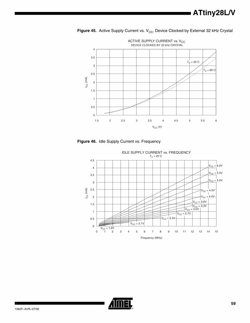
ATtiny28L/V
Figure 45. Active Supply Current vs. VCC, Device Clocked by External 32 kHz Crystal
Figure 46. Idle Supply Current vs. Frequency
ACTIVE SUPPLY CURRENT vs. VCCDEVICE CLOCKED BY 32 kHz CRYSTAL
I CC (
mA
)
VCC (V)
0
0.5
1
1.5
2
2.5
3
3.5
4
1.5 2 2.5 3 3.5 4 4.5 5 5.5 6
TA = 85˚C
TA = 25˚C
TA = 25˚C
I C
C (
mA
)
IDLE SUPPLY CURRENT vs. FREQUENCY
Frequency (MHz)
0
0.5
1
1.5
2
2.5
3
3.5
4
4.5
0 1 2 3 4 5 6 7 8 9 10 11 12 13 14 15VCC = 1.8V
VCC = 2.1V
VCC = 2.4V
VCC = 2.7V
VCC = 3.0VVCC = 3.3V
VCC = 3.6V
VCC = 4.0V
VCC = 4.5V
VCC = 5.0V
VCC = 5.5V
VCC = 6.0V
591062F–AVR–07/06

Figure 47. Idle Supply Current vs. VCC
Figure 48. Idle Supply Current vs. VCC, Device Clocked by Internal Oscillator
IDLE SUPPLY CURRENT vs. VCCFREQUENCY = 4 MHz
I CC (
mA
)
VCC (V)
0
0.2
0.4
0.6
0.8
1
1.2
1.4
1.5 2 2.5 3 3.5 4 4.5 5 5.5 6
TA = 85˚CTA = 25˚C
IDLE SUPPLY CURRENT vs. VccDEVICE CLOCKED BY 1.2MHz INTERNAL RC OSCILLATOR
Icc
(mA
)
Vcc(V)
T = 85˚CA
T = 25˚CA
0
0.1
0.2
0.3
0.4
0.5
0.6
0.7
1.5 2 2.5 3 3.5 4 4.5 5 5.5 6
60 ATtiny28L/V 1062F–AVR–07/06

ATtiny28L/V
Figure 49. Idle Supply Current vs. VCC, Device Clocked by External 32 kHz Crystal
Figure 50. Power-down Supply Current vs. VCC
IDLE SUPPLY CURRENT vs. VCCDEVICE CLOCKED BY 32 kHz CRYSTAL
I CC (
µA)
VCC (V)
0
5
10
15
20
25
30
1.5 2 2.5 3 3.5 4 4.5 5 5.5 6
TA = 25˚C
TA = 85˚C
POWER-DOWN SUPPLY CURRENT vs. VCCWATCHDOG TIMER DISABLED
I CC (
µA)
VCC (V)
0
0.5
1
1.5
2
2.5
3
1.5 2 2.5 3 3.5 4 4.5 5 5.5 6
TA = 70˚C
TA = 85˚C
TA = 45˚C
TA = 25˚C
611062F–AVR–07/06

Figure 51. Power-down Supply Current vs. VCC
Analog comparator offset voltage is measured as absolute offset.
Figure 52. Analog Comparator Offset Voltage vs. Common Mode Voltage (VCC = 5V)
POWER-DOWN SUPPLY CURRENT vs. VCCWATCHDOG TIMER ENABLED
I CC (
µA)
VCC (V)
0
10
20
30
40
50
60
70
1.5 2 2.5 3 3.5 4 4.5 5 5.5 6
TA = 85˚CTA = 25˚C
0
2
4
6
8
10
12
14
16
18
0 0.5 1 1.5 2 2.5 3 3.5 4 4.5 5
Common Mode Voltage (V)
Offs
et V
olta
ge (
mV
)
TA = 85˚C
TA = 25˚C
62 ATtiny28L/V 1062F–AVR–07/06

ATtiny28L/V
Figure 53. Analog Comparator Offset Voltage vs. Common Mode Voltage (VCC = 2.7V)
Figure 54. Analog Comparator Input Leakage Current (VCC = 6V; TA = 25°C)
0
2
4
6
8
10
0 0.5 1 1.5 2 2.5 3
Common Mode Voltage (V)
Offs
et V
olta
ge (
mV
)
TA = 25˚C
TA = 85˚C
60
50
40
30
20
10
0
-100 0.5 1.51 2 2.5 3.53 4 4.5 5 6 6.5 75.5
I AC
LK (
nA)
VIN (V)
631062F–AVR–07/06

Figure 55. Calibrated Internal RC Oscillator Frequency vs. VCC
Figure 56. Watchdog Oscillator Frequency vs. VCC
CALIBRATED RC OSCILLATOR FREQUENCY vs.
FR
c(M
Hz)
Vcc(V)
T = 45˚CA
T = 70˚CA
OPERATING VOLTAGE
1.1
1.12
1.14
1.16
1.18
1.2
1.22
1.24
1.26
1.28
2 2.5 3 3.5 4 4.5 5 5.5 6
T = 25˚CA
T = 85˚CA
0
200
400
600
800
1000
1200
1400
1600
1.5 2 2.5 3 3.5 4 4.5 5 5.5 6
VCC (V)
FR
C (
kHz)
TA = 85˚C
TA = 25˚C
64 ATtiny28L/V 1062F–AVR–07/06
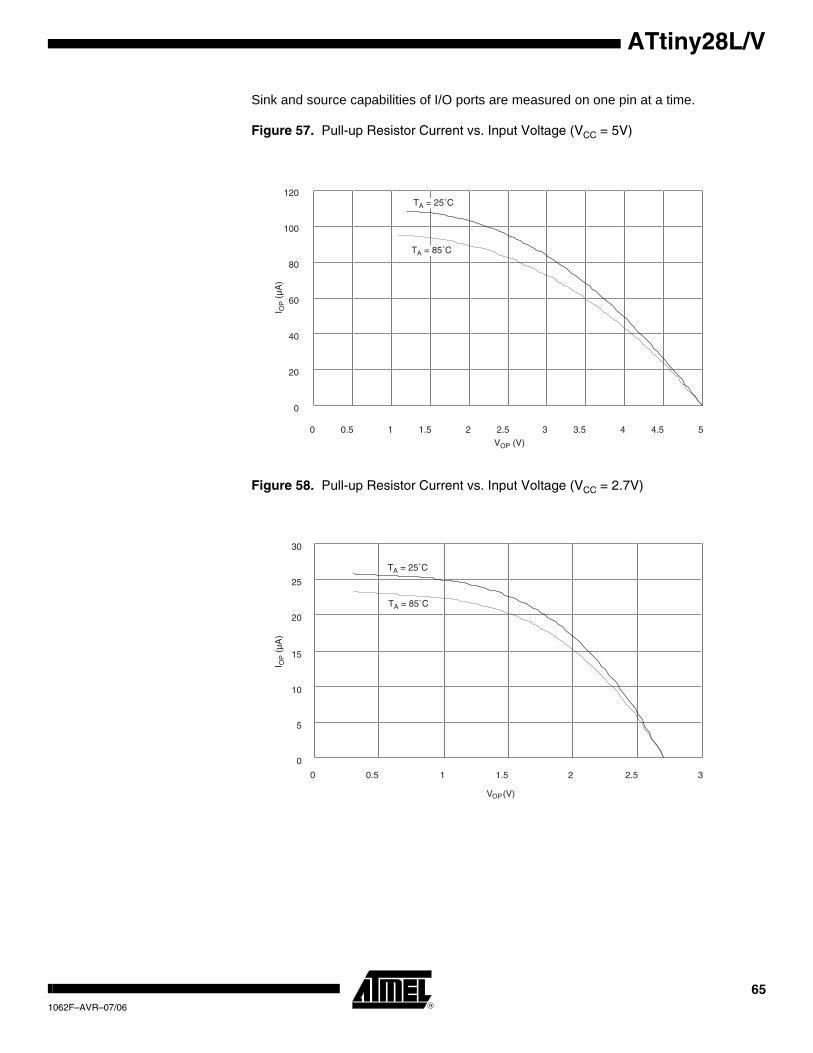
ATtiny28L/V
Sink and source capabilities of I/O ports are measured on one pin at a time.
Figure 57. Pull-up Resistor Current vs. Input Voltage (VCC = 5V)
Figure 58. Pull-up Resistor Current vs. Input Voltage (VCC = 2.7V)
0
20
40
60
80
100
120
0 0.5 1 1.5 2 2.5 3 3.5 4 4.5 5
I OP (
µA)
VOP (V)
TA = 85˚C
TA = 25˚C
0
5
10
15
20
25
30
0 0.5 1 1.5 2 2.5 3
I OP (
µA)
V (V)OP
TA = 25˚C
TA = 85˚C
651062F–AVR–07/06

Figure 59. I/O Pin Sink Current vs. Output Voltage. All pins except PA2 (VCC = 5V)
Figure 60. I/O Pin Source Current vs. Output voltage (VCC = 5V)
0
10
20
30
40
50
60
70
0 0.5 1 1.5 2 2.5 3
I OL
(mA
)
VOL (V)
TA = 25˚C
TA = 85˚C
0
2
4
6
8
10
12
14
16
18
20
0 0.5 1 1.5 2 2.5 3 3.5 4 4.5 5
I OH (
mA
)
VOH (V)
TA = 25˚C
TA = 85˚C
66 ATtiny28L/V 1062F–AVR–07/06

ATtiny28L/V
Figure 61. I/O Pin Sink Current vs. Output Voltage, All Pins Except PA2 (VCC = 2.7V)
Figure 62. I/O Pin Source Current vs. Output Voltage (VCC = 2.7V)
0
5
10
15
20
25
0 0.5 1 1.5 2
I OL
(mA
)
VOL (V)
TA = 25˚C
TA = 85˚C
0
1
2
3
4
5
6
0 0.5 1 1.5 2 2.5 3
I OH (
mA
)
VOH (V)
TA = 25˚C
TA = 85˚C
671062F–AVR–07/06

Figure 63. PA2 I/O Pin Sink Current vs. Output Voltage (High Current Pin PA2; TA =25°C)
Figure 64. I/O Pin Input Threshold Voltage vs. VCC (TA = 25°C)
0
10
20
30
40
50
60
70
80
90
0 0.5 1 1.5 2 2.5 3 3.5 4
VOL (V)
I OL
(mA
)
VCC = 1.8V
VCC = 3.6V
VCC = 2.4V
0
0.5
1
1.5
2
2.5
2.7 4.0 5.0
Thr
esho
ld V
olta
ge (
V)
VCC
68 ATtiny28L/V 1062F–AVR–07/06
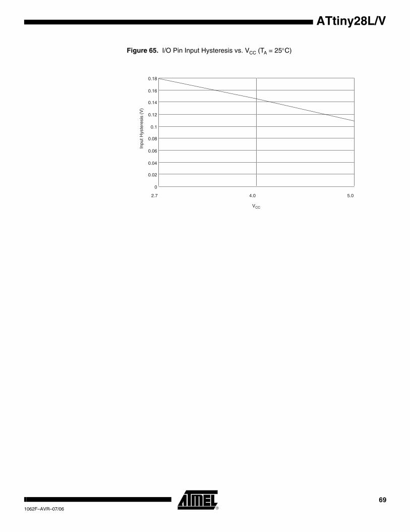
ATtiny28L/V
Figure 65. I/O Pin Input Hysteresis vs. VCC (TA = 25°C)
0
0.02
0.04
0.06
0.08
0.1
0.12
0.14
0.16
0.18
2.7 4.0 5.0
Inpu
t Hys
tere
sis
(V)
VCC
691062F–AVR–07/06
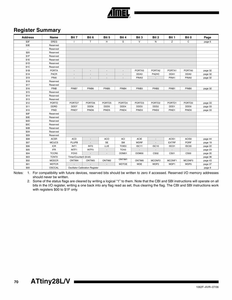
Notes: 1. For compatibility with future devices, reserved bits should be written to zero if accessed. Reserved I/O memory addressesshould never be written.
2. Some of the status flags are cleared by writing a logical “1” to them. Note that the CBI and SBI instructions will operate on allbits in the I/O register, writing a one back into any flag read as set, thus clearing the flag. The CBI and SBI instructions workwith registers $00 to $1F only.
Register SummaryAddress Name Bit 7 Bit 6 Bit 5 Bit 4 Bit 3 Bit 2 Bit 1 Bit 0 Page
$3F SREG I T H S V N Z C page 6
$3E Reserved
... Reserved
$20 Reserved
$1F Reserved
$1E Reserved
$1D Reserved
$1C Reserved
$1B PORTA - - - - PORTA3 PORTA2 PORTA1 PORTA0 page 32
$1A PACR - - - - DDA3 PA2HC DDA1 DDA0 page 32
$19 PINA - - - - PINA3 - PINA1 PINA0 page 32
$18 Reserved
$17 Reserved
$16 PINB PINB7 PINB6 PINB5 PINB4 PINB3 PINB2 PINB1 PINB0 page 32
$15 Reserved
$14 Reserved
$13 Reserved
$12 PORTD PORTD7 PORTD6 PORTD5 PORTD4 PORTD3 PORTD2 PORTD1 PORTD0 page 33
$11 DDRD DDD7 DDD6 DDD5 DDD4 DDD3 DDD2 DDD1 DDD0 page 33
$10 PIND PIND7 PIND6 PIND5 PIND4 PIND3 PIND2 PIND1 PIND0 page 33
$0F Reserved
$0E Reserved
$0D Reserved
$0C Reserved
$0B Reserved
$0A Reserved
$09 Reserved
$08 ACSR ACD - ACO ACI ACIE - ACIS1 ACIS0 page 44
$07 MCUCS PLUPB - SE SM WDRF - EXTRF PORF page 19
$06 ICR INT1 INT0 LLIE TOIE0 ISC11 ISC10 ISC01 ISC00 page 22
$05 IFR INTF1 INTF0 - TOV0 - - - - page 23
$04 TCCR0 FOV0 - - OOM01 OOM00 CS02 CS01 CS00 page 35
$03 TCNT0 Timer/Counter0 (8-bit) page 36
$02 MODCR ONTIM4 ONTIM3 ONTIM2 ONTIM1 ONTIM0 MCONF2 MCONF1 MCONF0 page 43
$01 WDTCR - - - WDTOE WDE WDP2 WDP1 WDP0 page 37
$00 OSCCAL Oscillator Calibration Register page 9
70 ATtiny28L/V 1062F–AVR–07/06

ATtiny28L/V
Instruction Set SummaryMnemonic Operands Description Operation Flags # Clocks
ARITHMETIC AND LOGIC INSTRUCTIONS
ADD Rd, Rr Add Two Registers Rd ← Rd + Rr Z,C,N,V,H 1
ADC Rd, Rr Add with Carry Two Registers Rd ← Rd + Rr + C Z,C,N,V,H 1
SUB Rd, Rr Subtract Two Registers Rd ← Rd - Rr Z,C,N,V,H 1
SUBI Rd, K Subtract Constant from Register Rd ← Rd - K Z,C,N,V,H 1
SBC Rd, Rr Subtract with Carry Two Registers Rd ← Rd - Rr - C Z,C,N,V,H 1
SBCI Rd, K Subtract with Carry Constant from Reg. Rd ← Rd - K - C Z,C,N,V,H 1
AND Rd, Rr Logical AND Registers Rd ← Rd • Rr Z,N,V 1
ANDI Rd, K Logical AND Register and Constant Rd ← Rd • K Z,N,V 1
OR Rd, Rr Logical OR Registers Rd ← Rd v Rr Z,N,V 1
ORI Rd, K Logical OR Register and Constant Rd ← Rd v K Z,N,V 1
EOR Rd, Rr Exclusive OR Registers Rd ← Rd ⊕ Rr Z,N,V 1
COM Rd One’s Complement Rd ← $FF - Rd Z,C,N,V 1
NEG Rd Two’s Complement Rd ← $00 - Rd Z,C,N,V,H 1
SBR Rd, K Set Bit(s) in Register Rd ← Rd v K Z,N,V 1
CBR Rd, K Clear Bit(s) in Register Rd ← Rd • (FFh - K) Z,N,V 1
INC Rd Increment Rd ← Rd + 1 Z,N,V 1
DEC Rd Decrement Rd ← Rd - 1 Z,N,V 1
TST Rd Test for Zero or Minus Rd ← Rd • Rd Z,N,V 1
CLR Rd Clear Register Rd ← Rd ⊕ Rd Z,N,V 1
SER Rd Set Register Rd ← $FF None 1
BRANCH INSTRUCTIONS
RJMP k Relative Jump PC ← PC + k + 1 None 2
RCALL k Relative Subroutine Call PC ← PC + k + 1 None 3
RET Subroutine Return PC ← STACK None 4
RETI Interrupt Return PC ← STACK I 4
CPSE Rd, Rr Compare, Skip if Equal if (Rd = Rr) PC ← PC + 2 or 3 None 1/2
CP Rd, Rr Compare Rd - Rr Z,N,V,C,H 1
CPC Rd, Rr Compare with Carry Rd - Rr - C Z,N,V,C,H 1
CPI Rd, K Compare Register with Immediate Rd - K Z N,V,C,H 1
SBRC Rr, b Skip if Bit in Register Cleared if (Rr(b) = 0) PC ← PC + 2 or 3 None 1/2
SBRS Rr, b Skip if Bit in Register is Set if (Rr(b) = 1) PC ← PC + 2 or 3 None 1/2
SBIC P, b Skip if Bit in I/O Register Cleared if (P(b) = 0) PC ← PC + 2 or 3 None 1/2
SBIS P, b Skip if Bit in I/O Register is Set if (P(b) = 1) PC ← PC + 2 or 3 None 1/2
BRBS s, k Branch if Status Flag Set if (SREG(s) = 1) then PC ← PC + k + 1 None 1/2
BRBC s, k Branch if Status Flag Cleared if (SREG(s) = 0) then PC ← PC + k + 1 None 1/2
BREQ k Branch if Equal if (Z = 1) then PC ← PC + k + 1 None 1/2
BRNE k Branch if Not Equal if (Z = 0) then PC ← PC + k + 1 None 1/2
BRCS k Branch if Carry Set if (C = 1) then PC ← PC + k + 1 None 1/2
BRCC k Branch if Carry Cleared if (C = 0) then PC ← PC + k + 1 None 1/2
BRSH k Branch if Same or Higher if (C = 0) then PC ← PC + k + 1 None 1/2
BRLO k Branch if Lower if (C = 1) then PC ← PC + k + 1 None 1/2
BRMI k Branch if Minus if (N = 1) then PC ← PC + k + 1 None 1/2
BRPL k Branch if Plus if (N = 0) then PC ← PC + k + 1 None 1/2
BRGE k Branch if Greater or Equal, Signed if (N ⊕ V = 0) then PC ← PC + k + 1 None 1/2
BRLT k Branch if Less than Zero, Signed if (N ⊕ V = 1) then PC ← PC + k + 1 None 1/2
BRHS k Branch if Half-carry Flag Set if (H = 1) then PC ← PC + k + 1 None 1/2
BRHC k Branch if Half-carry Flag Cleared if (H = 0) then PC ← PC + k + 1 None 1/2
BRTS k Branch if T-flag Set if (T = 1) then PC ← PC + k + 1 None 1/2
BRTC k Branch if T-flag Cleared if (T = 0) then PC ← PC + k + 1 None 1/2
BRVS k Branch if Overflow Flag is Set if (V = 1) then PC ← PC + k + 1 None 1/2
BRVC k Branch if Overflow Flag is Cleared if (V = 0) then PC ← PC + k + 1 None 1/2
BRIE k Branch if Interrupt Enabled if (I = 1) then PC ← PC + k + 1 None 1/2
BRID k Branch if Interrupt Disabled if (I = 0) then PC ← PC + k + 1 None 1/2
711062F–AVR–07/06

DATA TRANSFER INSTRUCTIONS
LD Rd, Z Load Register Indirect Rd ← (Z) None 2
ST Z, Rr Store Register Indirect (Z) ← Rr None 2
MOV Rd, Rr Move between Registers Rd ← Rr None 1
LDI Rd, K Load Immediate Rd ← K None 1
IN Rd, P In Port Rd ← P None 1
OUT P, Rr Out Port P ← Rr None 1
LPM Load Program Memory R0 ← (Z) None 3
BIT AND BIT-TEST INSTRUCTIONS
SBI P, b Set Bit in I/O Register I/O(P,b) ← 1 None 2
CBI P, b Clear Bit in I/O Register I/O(P,b) ← 0 None 2
LSL Rd Logical Shift Left Rd(n+1) ← Rd(n), Rd(0) ← 0 Z,C,N,V 1
LSR Rd Logical Shift Right Rd(n) ← Rd(n+1), Rd(7) ← 0 Z,C,N,V 1
ROL Rd Rotate Left through Carry Rd(0) ← C, Rd(n+1) ← Rd(n), C ← Rd(7) Z,C,N,V 1
ROR Rd Rotate Right through Carry Rd(7) ← C, Rd(n) ← Rd(n+1), C ← Rd(0) Z,C,N,V 1
ASR Rd Arithmetic Shift Right Rd(n) ← Rd(n+1), n = 0..6 Z,C,N,V 1
SWAP Rd Swap Nibbles Rd(3..0) ← Rd(7..4), Rd(7..4) ← Rd(3..0) None 1
BSET s Flag Set SREG(s) ← 1 SREG(s) 1
BCLR s Flag Clear SREG(s) ← 0 SREG(s) 1
BST Rr, b Bit Store from Register to T T ← Rr(b) T 1
BLD Rd, b Bit Load from T to Register Rd(b) ← T None 1
SEC Set Carry C ← 1 C 1
CLC Clear Carry C ← 0 C 1
SEN Set Negative Flag N ← 1 N 1
CLN Clear Negative Flag N ← 0 N 1
SEZ Set Zero Flag Z ← 1 Z 1
CLZ Clear Zero Flag Z ← 0 Z 1
SEI Global Interrupt Enable I ← 1 I 1
CLI Global Interrupt Disable I ← 0 I 1
SES Set Signed Test Flag S ← 1 S 1
CLS Clear Signed Test Flag S ← 0 S 1
SEV Set Two’s Complement Overflow V ← 1 V 1
CLV Clear Two’s Complement Overflow V ← 0 V 1
SET Set T in SREG T ← 1 T 1
CLT Clear T in SREG T ← 0 T 1
SEH Set Half-carry Flag in SREG H ← 1 H 1
CLH Clear Half-carry Flag in SREG H ← 0 H 1
NOP No Operation None 1
SLEEP Sleep (see specific descr. for Sleep function) None 1
WDR Watchdog Reset (see specific descr. for WDR/timer) None 1
Instruction Set Summary (Continued)Mnemonic Operands Description Operation Flags # Clocks
72 ATtiny28L/V 1062F–AVR–07/06

ATtiny28L/V
Notes: 1. This device can also be supplied in wafer form. Please contact your local Atmel sales office for detailed ordering informationand minimum quantities.
2. Pb-free packaging alternative, complies to the European Directive for Restriction of Hazardous Substances (RoHS direc-tive).Also Halide free and fully Green.
Ordering InformationSpeed (MHz) Power Supply (Volts) Ordering Code Package(1) Operation Range
4 2.7 - 5.5
ATtiny28L-4ACATtiny28L-4PCATtiny28L-4MC
32A28P332M1-A
Commercial
(0°C to 70°C)
ATtiny28L-4AI
ATtiny28L-4AU(2)
ATtiny28L-4PI
ATtiny28L-4PU(2)
ATtiny28L-4MIATtiny28L-4MU(2)
32A
32A28P3
28P3
32M1-A32M1-A
Industrial
(-40°C to 85°C)
1.2 1.8 - 5.5
ATtiny28V-1ACATtiny28V-1PCATtiny28V-1MC
32A28P332M1-A
Commercial
(0°C to 70°C)
ATtiny28V-1AI
ATtiny28V-1AU(2)
ATtiny28V-1PI
ATtiny28V-1PU(2)
ATtiny28V-1MIATtiny28V-1MU(2)
32A32A
28P3
28P332M1-A
32M1-A
Industrial
(-40°C to 85°C)
Package Type
32A 32-lead, Thin (1.0 mm) Plastic Quad Flat Package (TQFP)
28P3 28-lead, 0.300" Wide, Plastic Dual Inline Package (PDIP)
32M1-A 32-pad, 5x5x1.0 body, Lead Pitch 0.50mm, Quad Flat No-lead/Micro Lead Frame Package (QFN/MLF)
731062F–AVR–07/06

Packaging Information
32A
2325 Orchard Parkway San Jose, CA 95131
TITLE DRAWING NO.
R
REV.
32A, 32-lead, 7 x 7 mm Body Size, 1.0 mm Body Thickness,0.8 mm Lead Pitch, Thin Profile Plastic Quad Flat Package (TQFP)
B32A
10/5/2001
PIN 1 IDENTIFIER
0˚~7˚
PIN 1
L
C
A1 A2 A
D1
D
e E1 E
B
Notes: 1. This package conforms to JEDEC reference MS-026, Variation ABA. 2. Dimensions D1 and E1 do not include mold protrusion. Allowable
protrusion is 0.25 mm per side. Dimensions D1 and E1 are maximum plastic body size dimensions including mold mismatch.
3. Lead coplanarity is 0.10 mm maximum.
A – – 1.20
A1 0.05 – 0.15
A2 0.95 1.00 1.05
D 8.75 9.00 9.25
D1 6.90 7.00 7.10 Note 2
E 8.75 9.00 9.25
E1 6.90 7.00 7.10 Note 2
B 0.30 – 0.45
C 0.09 – 0.20
L 0.45 – 0.75
e 0.80 TYP
COMMON DIMENSIONS(Unit of Measure = mm)
SYMBOL MIN NOM MAX NOTE
74 ATtiny28L/V 1062F–AVR–07/06

ATtiny28L/V
28P3
2325 Orchard Parkway San Jose, CA 95131
TITLE DRAWING NO.
R
REV. 28P3, 28-lead (0.300"/7.62 mm Wide) Plastic Dual Inline Package (PDIP) B28P3
09/28/01
PIN1
E1
A1
B
REF
E
B1
C
L
SEATING PLANE
A
0º ~ 15º
D
e
eB
B2(4 PLACES)
COMMON DIMENSIONS(Unit of Measure = mm)
SYMBOL MIN NOM MAX NOTE
A – – 4.5724
A1 0.508 – –
D 34.544 – 34.798 Note 1
E 7.620 – 8.255
E1 7.112 – 7.493 Note 1
B 0.381 – 0.533
B1 1.143 – 1.397
B2 0.762 – 1.143
L 3.175 – 3.429
C 0.203 – 0.356
eB – – 10.160
e 2.540 TYP
Note: 1. Dimensions D and E1 do not include mold Flash or Protrusion.Mold Flash or Protrusion shall not exceed 0.25 mm (0.010").
751062F–AVR–07/06
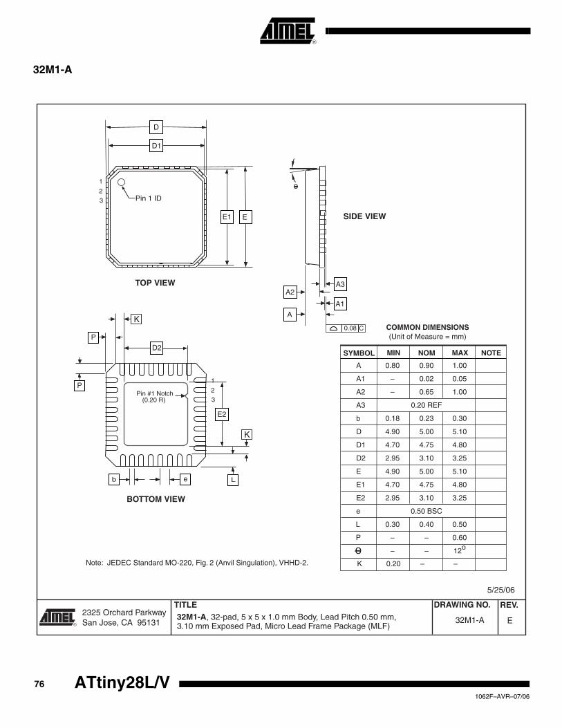
32M1-A
2325 Orchard Parkway San Jose, CA 95131
TITLE DRAWING NO.
R
REV. 32M1-A, 32-pad, 5 x 5 x 1.0 mm Body, Lead Pitch 0.50 mm, E32M1-A
5/25/06
3.10 mm Exposed Pad, Micro Lead Frame Package (MLF)
COMMON DIMENSIONS(Unit of Measure = mm)
SYMBOL MIN NOM MAX NOTE
D1
D
E1 E
eb
A3A2
A1 A
D2
E2
0.08 C
L
1
2
3
P
P
01
2
3
A 0.80 0.90 1.00
A1 – 0.02 0.05
A2 – 0.65 1.00
A3 0.20 REF
b 0.18 0.23 0.30
D
D1
D2 2.95 3.10 3.25
4.90 5.00 5.10
4.70 4.75 4.80
4.70 4.75 4.80
4.90 5.00 5.10
E
E1
E2 2.95 3.10 3.25
e 0.50 BSC
L 0.30 0.40 0.50
P – – 0.60
– – 12o
Note: JEDEC Standard MO-220, Fig. 2 (Anvil Singulation), VHHD-2.
TOP VIEW
SIDE VIEW
BOTTOM VIEW
0
Pin 1 ID
Pin #1 Notch(0.20 R)
K 0.20 – –
K
K
76 ATtiny28L/V 1062F–AVR–07/06

ATtiny28L/V
Errata
All revisions No known errata.
771062F–AVR–07/06

Datasheet Revision History
Please note that the referring page numbers in this section are referred to this docu-ment. The referring revision in this section are referring to the document revision.
Rev – 01/06G 1. Updated chapter layout.
2. Updated “Ordering Information” on page 73.
Rev – 01/06G 1. Updated description for “Port A” on page 25.
2. Added note 6 in “DC Characteristics” on page 54.
3. Updated “Ordering Information” on page 73.
4. Added “Errata” on page 77.
Rev – 03/05F 1. Updated “Electrical Characteristics” on page 54.
2. MLF-package alternative changed to “Quad Flat No-Lead/Micro Lead Frame Package QFN/MLF”.
3. Updated “Ordering Information” on page 73.
78 ATtiny28L/V 1062F–AVR–07/06

ATtiny28L/V
Table of Contents Features................................................................................................. 1
Pin Configurations................................................................................ 1
Description ............................................................................................ 2Block Diagram ...................................................................................................... 2Pin Descriptions.................................................................................................... 3Clock Options ....................................................................................................... 4
Architectural Overview......................................................................... 6General-purpose Register File.............................................................................. 7ALU – Arithmetic Logic Unit.................................................................................. 7Downloadable Flash Program Memory ................................................................ 7Program and Data Addressing Modes.................................................................. 7Subroutine and Interrupt Hardware Stack .......................................................... 10Memory Access and Instruction Execution Timing ............................................. 10I/O Memory ......................................................................................................... 11Reset and Interrupt Handling.............................................................................. 12Sleep Modes....................................................................................................... 21
Timer/Counter0 ................................................................................... 24Timer/Counter Prescaler..................................................................................... 24
Watchdog Timer.................................................................................. 27
Calibrated Internal RC Oscillator ...................................................... 29
Hardware Modulator ........................................................................... 30
Analog Comparator ............................................................................ 35
I/O Ports............................................................................................... 37Port A.................................................................................................................. 37Port B.................................................................................................................. 40Port D.................................................................................................................. 43
Memory Programming........................................................................ 45Program Memory Lock Bits ................................................................................ 45Fuse Bits............................................................................................................. 45Signature Bytes .................................................................................................. 45Calibration Byte .................................................................................................. 45Programming the Flash ...................................................................................... 45Parallel Programming ......................................................................................... 46
Parallel Programming Characteristics.............................................. 52
i1062F–AVR–07/06

Electrical Characteristics................................................................... 53Absolute Maximum Ratings ................................................................................ 53DC Characteristics.............................................................................................. 53External Clock Drive Waveforms ........................................................................ 55External Clock Drive ........................................................................................... 55
Typical Characteristics ...................................................................... 56
Register Summary .............................................................................. 69
Instruction Set Summary ................................................................... 70
Ordering Information.......................................................................... 72
Packaging Information ....................................................................... 7432A ..................................................................................................................... 7428P3 ................................................................................................................... 7532M1-A ............................................................................................................... 76
Errata ................................................................................................... 77All revisions......................................................................................................... 77
Datasheet Revision History ............................................................... 78Rev – 01/06G...................................................................................................... 78Rev – 03/05F ...................................................................................................... 78
Table of Contents .................................................................................. i
ii ATtiny28L/V1062F–AVR–07/06

Printed on recycled paper.
1062F–AVR–07/06
© Atmel Corporation 2006. All rights reserved. Atmel®, logo and combinations thereof, Everywhere You Are®, AVR®, AVR Studio®, and oth-ers, are registered trademarks or trademarks of Atmel Corporation or its subsidiaries. Other terms and product names may be trademarks of oth-ers.
Disclaimer: The information in this document is provided in connection with Atmel products. No license, express or implied, by estoppel or otherwise, to anyintellectual property right is granted by this document or in connection with the sale of Atmel products. EXCEPT AS SET FORTH IN ATMEL’S TERMS AND CONDI-TIONS OF SALE LOCATED ON ATMEL’S WEB SITE, ATMEL ASSUMES NO LIABILITY WHATSOEVER AND DISCLAIMS ANY EXPRESS, IMPLIED OR STATUTORYWARRANTY RELATING TO ITS PRODUCTS INCLUDING, BUT NOT LIMITED TO, THE IMPLIED WARRANTY OF MERCHANTABILITY, FITNESS FOR A PARTICULARPURPOSE, OR NON-INFRINGEMENT. IN NO EVENT SHALL ATMEL BE LIABLE FOR ANY DIRECT, INDIRECT, CONSEQUENTIAL, PUNITIVE, SPECIAL OR INCIDEN-TAL DAMAGES (INCLUDING, WITHOUT LIMITATION, DAMAGES FOR LOSS OF PROFITS, BUSINESS INTERRUPTION, OR LOSS OF INFORMATION) ARISING OUTOF THE USE OR INABILITY TO USE THIS DOCUMENT, EVEN IF ATMEL HAS BEEN ADVISED OF THE POSSIBILITY OF SUCH DAMAGES. Atmel makes norepresentations or warranties with respect to the accuracy or completeness of the contents of this document and reserves the right to make changes to specificationsand product descriptions at any time without notice. Atmel does not make any commitment to update the information contained herein. Unless specifically providedotherwise, Atmel products are not suitable for, and shall not be used in, automotive applications. Atmel’s products are not intended, authorized, or warranted for useas components in applications intended to support or sustain life.
Atmel Corporation Atmel Operations
2325 Orchard ParkwaySan Jose, CA 95131, USATel: 1(408) 441-0311Fax: 1(408) 487-2600
Regional Headquarters
EuropeAtmel SarlRoute des Arsenaux 41Case Postale 80CH-1705 FribourgSwitzerlandTel: (41) 26-426-5555Fax: (41) 26-426-5500
AsiaRoom 1219Chinachem Golden Plaza77 Mody Road TsimshatsuiEast KowloonHong KongTel: (852) 2721-9778Fax: (852) 2722-1369
Japan9F, Tonetsu Shinkawa Bldg.1-24-8 ShinkawaChuo-ku, Tokyo 104-0033JapanTel: (81) 3-3523-3551Fax: (81) 3-3523-7581
Memory2325 Orchard ParkwaySan Jose, CA 95131, USATel: 1(408) 441-0311Fax: 1(408) 436-4314
Microcontrollers2325 Orchard ParkwaySan Jose, CA 95131, USATel: 1(408) 441-0311Fax: 1(408) 436-4314
La ChantrerieBP 7060244306 Nantes Cedex 3, FranceTel: (33) 2-40-18-18-18Fax: (33) 2-40-18-19-60
ASIC/ASSP/Smart CardsZone Industrielle13106 Rousset Cedex, FranceTel: (33) 4-42-53-60-00Fax: (33) 4-42-53-60-01
1150 East Cheyenne Mtn. Blvd.Colorado Springs, CO 80906, USATel: 1(719) 576-3300Fax: 1(719) 540-1759
Scottish Enterprise Technology ParkMaxwell BuildingEast Kilbride G75 0QR, Scotland Tel: (44) 1355-803-000Fax: (44) 1355-242-743
RF/AutomotiveTheresienstrasse 2Postfach 353574025 Heilbronn, GermanyTel: (49) 71-31-67-0Fax: (49) 71-31-67-2340
1150 East Cheyenne Mtn. Blvd.Colorado Springs, CO 80906, USATel: 1(719) 576-3300Fax: 1(719) 540-1759
Biometrics/Imaging/Hi-Rel MPU/High Speed Converters/RF Datacom
Avenue de RochepleineBP 12338521 Saint-Egreve Cedex, FranceTel: (33) 4-76-58-30-00Fax: (33) 4-76-58-34-80
Literature Requestswww.atmel.com/literature