500-madual differential line driver - ti.com
TRANSCRIPT

VCC−1OUTVCC+1IN+1IN−
NCNCNCNCNC
VCC −2OUTVCC+2IN+2IN−NCNCNCNCNC
123
4 56789
10
201918
171615141312
11
Cross Section View Showing PowerPAD
Thermally Enhanced SOIC (DWP) PowerPADPackage
(TOP VIEW)
(SIDE VIEW)
MicroStar Junior (GQE) Package(TOP VIEW)
THS6012
www.ti.com SLOS226F –SEPTEMBER 1998–REVISED JUNE 2012
500-mA DUAL DIFFERENTIAL LINE DRIVERCheck for Samples: THS6012
1FEATURES2• ADSL Differential Line Driver• 400 mA Minimum Output Current Into 25-Ω
Load• High Speed
– 140 MHz Bandwidth (-3dB) With 25-Ω Load– 315 MHz Bandwidth (-3dB) With 100-Ω Load– 1300 V/μs Slew Rate, G = 5
• Low Distortion– -72 dB 3rd Order Harmonic Distortion at
f = 1 MHz, 25-Ω Load, and 20 VPP
• Independent Power Supplies for LowCrosstalk
• Wide Supply Range ±4.5 V to ±16 V• Thermal Shutdown and Short Circuit
Protection• Improved Replacement for AD815• Evaluation Module Available
DESCRIPTIONThe THS6012 contains two high-speed driverscapable of providing 400 mA output current (min) intoa 25 Ω load. These drivers can be configureddifferentially to drive a 50-VPP output signal over low-impedance lines. The drivers are current feedbackamplifiers, designed for the high slew rates necessaryto support low total harmonic distortion (THD) inxDSL applications. The THS6012 is ideally suited forasymmetrical digital subscriber line (ADSL)
HIGH-SPEED xDSL LINE DRIVER/RECEIVERapplications at the central office, where it supportsFAMILYthe high-peak voltage and current requirements of
DEVICE DRIVER RECEIVER DESCRIPTIONthis application.Dual differential line drivers andTHS6002 • •Separate power supply connections for each driver receivers
are provided to minimize crosstalk. The THS6012 is THS6012 • 500-mA Dual differential line driveravailable in the small surface-mount, thermally
THS6022 • 250-mA Dual differential line driverenhanced 20-pin PowerPAD™ package.
Low-power ADSL central office lineTHS6032 • driver
THS6062 • Low-noise ADSL receiver
Low-noise programmable gain ADSLTHS7002 • receiver
1
Please be aware that an important notice concerning availability, standard warranty, and use in critical applications ofTexas Instruments semiconductor products and disclaimers thereto appears at the end of this data sheet.
2PowerPAD is a trademark of Texas Instruments.
PRODUCTION DATA information is current as of publication date. Copyright © 1998–2012, Texas Instruments IncorporatedProducts conform to specifications per the terms of the TexasInstruments standard warranty. Production processing does notnecessarily include testing of all parameters.

_
+
Driver 1
Driver 2
_
+
3
4
5
17
16
2
1
18
19
20
VCC+
VCC+
VCC–
VCC–
1OUT
2OUT
1IN+
1IN–
2IN+
2IN–
THS6012
SLOS226F –SEPTEMBER 1998–REVISED JUNE 2012 www.ti.com
These devices have limited built-in ESD protection. The leads should be shorted together or the device placed in conductive foamduring storage or handling to prevent electrostatic damage to the MOS gates.
Table 1. AVAILABLE OPTIONS
PACKAGED DEVICE
PowerPAD PLASTICTA MicroStar Junior EVALUATIONSMALL OUTLINE (1)(GQE) MODULE(DWP)
0°C to 70°C THS6012CDWP THS6012CGQE THS6012EVM
-40°C to 85°C THS6012IDWP THS6012IGQE —
(1) The PWP packages are available taped and reeled. Add an R suffix to the device type (i.e.,THS6012CPWPR)
FUNCTIONAL BLOCK DIAGRAM
2 Copyright © 1998–2012, Texas Instruments Incorporated

98765
A
B
C
D
E
F
321
G
H
J
4
2IN+1N+
1IN–
NC
NC
NC
NC
NC
NCNC NC NC NC
NC NC NC
NC NC NC
NC NC NC
NC NC
NC NC NC
VCC+NCNC
NCNC
NC
NC
NCNC NC
NCNC NC
NC NC
NC NC
NC
NC
NC
NC
NC NC
NC
2OU
T
NC
NC
NC NCNC NC
NC
NC NC NC
NC
NC
1OU
T
NC NC
2IN–
NC
NCNC
NC
VCC+
NOTE: Shaded terminals are used for thermal connection to the ground plane.
MicroStar Junior (GQE) Package(TOP VIEW)
VC
C–
VC
C–
NC
NCNCNC
NC
THS6012
www.ti.com SLOS226F –SEPTEMBER 1998–REVISED JUNE 2012
Terminal FunctionsTERMINAL
NAME DWP PACKAGE NO. GQE PACKAGE NO.
1OUT 2 A3
1IN- 5 F1
1IN+ 4 D1
2OUT 19 A7
2IN- 16 F9
2IN+ 17 D9
VCC+ 3, 18 B1, B9
VCC- 1, 20 A4, A6
6, 7, 8 ,9, 10, 11, 12, 13,NC NA14, 15
PIN ASSIGNMENTS
Copyright © 1998–2012, Texas Instruments Incorporated 3
THS6012
SLOS226F –SEPTEMBER 1998–REVISED JUNE 2012 www.ti.com
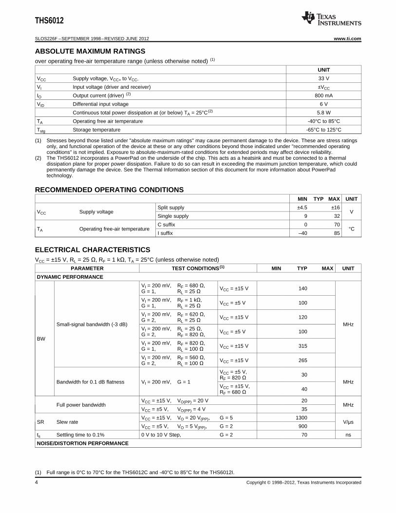
ABSOLUTE MAXIMUM RATINGSover operating free-air temperature range (unless otherwise noted) (1)
UNIT
VCC Supply voltage, VCC+ to VCC- 33 V
VI Input voltage (driver and receiver) ±VCC
IO Output current (driver) (2) 800 mA
VID Differential input voltage 6 V
Continuous total power dissipation at (or below) TA = 25°C (2) 5.8 W
TA Operating free air temperature -40°C to 85°C
Tstg Storage temperature -65°C to 125°C
(1) Stresses beyond those listed under "absolute maximum ratings" may cause permanent damage to the device. These are stress ratingsonly, and functional operation of the device at these or any other conditions beyond those indicated under "recommended operatingconditions" is not implied. Exposure to absolute-maximum-rated conditions for extended periods may affect device reliability.
(2) The THS6012 incorporates a PowerPad on the underside of the chip. This acts as a heatsink and must be connected to a thermaldissipation plane for proper power dissipation. Failure to do so can result in exceeding the maximum junction temperature, which couldpermanently damage the device. See the Thermal Information section of this document for more information about PowerPadtechnology.
RECOMMENDED OPERATING CONDITIONSMIN TYP MAX UNIT
Split supply ±4.5 ±16VCC Supply voltage V
Single supply 9 32
C suffix 0 70TA Operating free-air temperature °C
I suffix –40 85
ELECTRICAL CHARACTERISTICSVCC = ±15 V, RL = 25 Ω, RF = 1 kΩ, TA = 25°C (unless otherwise noted)
PARAMETER TEST CONDITIONS (1) MIN TYP MAX UNIT
DYNAMIC PERFORMANCE
VI = 200 mV, RF = 680 Ω, VCC = ±15 V 140G = 1, RL = 25 ΩVI = 200 mV, RF = 1 kΩ, VCC = ±5 V 100G = 1, RL = 25 ΩVI = 200 mV, RF = 620 Ω, VCC = ±15 V 120G = 2, RL = 25 Ω
Small-signal bandwidth (-3 dB) MHzVI = 200 mV, RL = 25 Ω, VCC = ±5 V 100G = 2, RF = 820 Ω,
BWVI = 200 mV, RF = 820 Ω, VCC = ±15 V 315G = 1, RL = 100 ΩVI = 200 mV, RF = 560 Ω, VCC = ±15 V 265G = 2, RL = 100 Ω
VCC = ±5 V, 30RF = 820 ΩBandwidth for 0.1 dB flatness VI = 200 mV, G = 1 MHz
VCC = ±15 V, 40RF = 680 ΩVCC = ±15 V, VO(PP) = 20 V 20
Full power bandwidth MHzVCC = ±5 V, VO(PP) = 4 V 35
VCC = ±15 V, VO = 20 V(PP), G = 5 1300SR Slew rate V/μs
VCC = ±5 V, VO = 5 V(PP), G = 2 900
ts Settling time to 0.1% 0 V to 10 V Step, G = 2 70 ns
NOISE/DISTORTION PERFORMANCE
(1) Full range is 0°C to 70°C for the THS6012C and -40°C to 85°C for the THS6012I.
4 Copyright © 1998–2012, Texas Instruments Incorporated
THS6012
www.ti.com SLOS226F –SEPTEMBER 1998–REVISED JUNE 2012
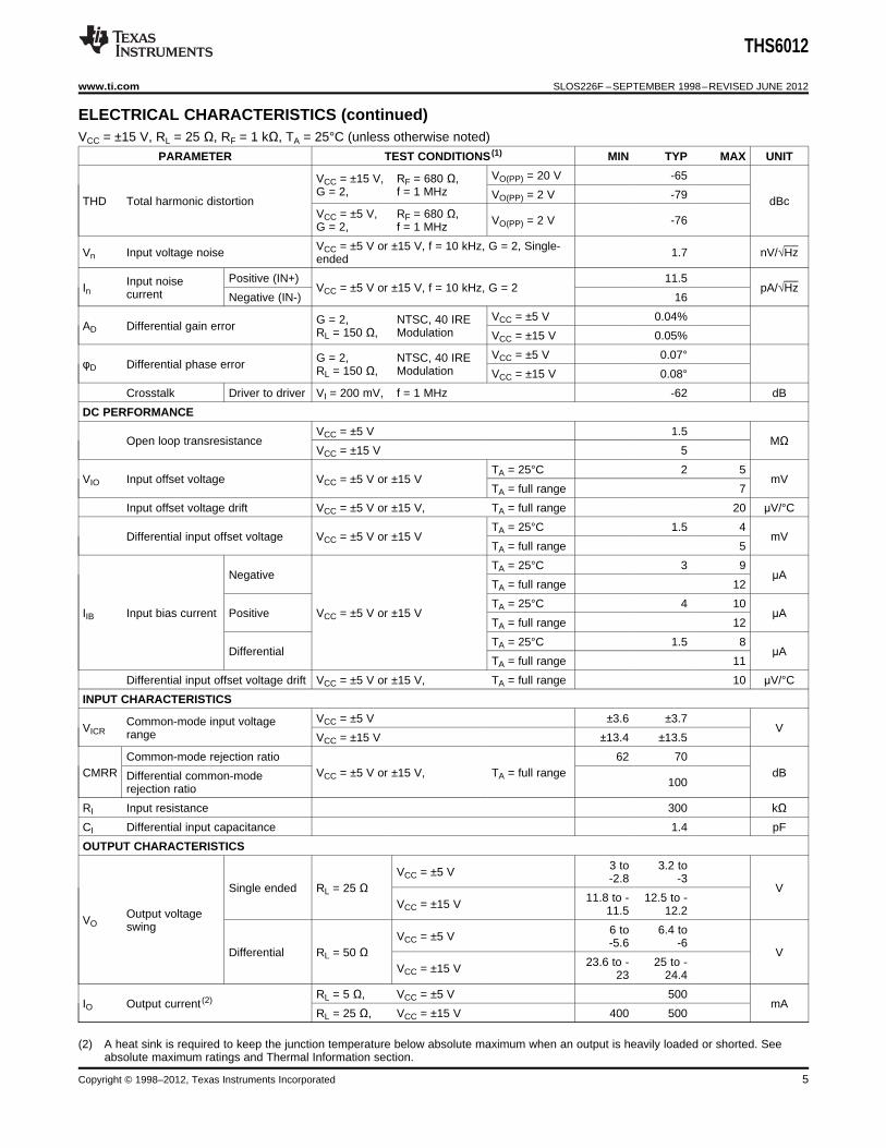
ELECTRICAL CHARACTERISTICS (continued)VCC = ±15 V, RL = 25 Ω, RF = 1 kΩ, TA = 25°C (unless otherwise noted)
PARAMETER TEST CONDITIONS (1) MIN TYP MAX UNIT
VO(PP) = 20 V -65VCC = ±15 V, RF = 680 Ω,G = 2, f = 1 MHz VO(PP) = 2 V -79THD Total harmonic distortion dBcVCC = ±5 V, RF = 680 Ω, VO(PP) = 2 V -76G = 2, f = 1 MHz
VCC = ±5 V or ±15 V, f = 10 kHz, G = 2, Single-Vn Input voltage noise 1.7 nV/√Hzended
Positive (IN+) 11.5Input noiseIn VCC = ±5 V or ±15 V, f = 10 kHz, G = 2 pA/√Hzcurrent Negative (IN-) 16
VCC = ±5 V 0.04%G = 2, NTSC, 40 IREAD Differential gain error RL = 150 Ω, Modulation VCC = ±15 V 0.05%
VCC = ±5 V 0.07°G = 2, NTSC, 40 IREφD Differential phase error RL = 150 Ω, Modulation VCC = ±15 V 0.08°
Crosstalk Driver to driver VI = 200 mV, f = 1 MHz -62 dB
DC PERFORMANCE
VCC = ±5 V 1.5Open loop transresistance MΩ
VCC = ±15 V 5
TA = 25°C 2 5VIO Input offset voltage VCC = ±5 V or ±15 V mV
TA = full range 7
Input offset voltage drift VCC = ±5 V or ±15 V, TA = full range 20 μV/°C
TA = 25°C 1.5 4Differential input offset voltage VCC = ±5 V or ±15 V mV
TA = full range 5
TA = 25°C 3 9Negative μA
TA = full range 12
TA = 25°C 4 10IIB Input bias current Positive VCC = ±5 V or ±15 V μA
TA = full range 12
TA = 25°C 1.5 8Differential μA
TA = full range 11
Differential input offset voltage drift VCC = ±5 V or ±15 V, TA = full range 10 μV/°C
INPUT CHARACTERISTICS
VCC = ±5 V ±3.6 ±3.7Common-mode input voltageVICR Vrange VCC = ±15 V ±13.4 ±13.5
Common-mode rejection ratio 62 70CMRR VCC = ±5 V or ±15 V, TA = full range dBDifferential common-mode 100rejection ratio
RI Input resistance 300 kΩCI Differential input capacitance 1.4 pF
OUTPUT CHARACTERISTICS
3 to 3.2 toVCC = ±5 V -2.8 -3Single ended RL = 25 Ω V
11.8 to - 12.5 to -VCC = ±15 V 11.5 12.2Output voltageVO swing 6 to 6.4 toVCC = ±5 V -5.6 -6Differential RL = 50 Ω V
23.6 to - 25 to -VCC = ±15 V 23 24.4
RL = 5 Ω, VCC = ±5 V 500IO Output current (2) mA
RL = 25 Ω, VCC = ±15 V 400 500
(2) A heat sink is required to keep the junction temperature below absolute maximum when an output is heavily loaded or shorted. Seeabsolute maximum ratings and Thermal Information section.
Copyright © 1998–2012, Texas Instruments Incorporated 5
VIVO+
–
RG RF
RL25 Ω
50 Ω–15 V
15 V
+
–
1 kΩ
VIVO
25 Ω50 Ω
1 kΩ
Driver 1+
–
1 kΩ
VIVO
25 Ω50 Ω
1 kΩ
Driver 2
THS6012
SLOS226F –SEPTEMBER 1998–REVISED JUNE 2012 www.ti.com
ELECTRICAL CHARACTERISTICS (continued)VCC = ±15 V, RL = 25 Ω, RF = 1 kΩ, TA = 25°C (unless otherwise noted)
PARAMETER TEST CONDITIONS (1) MIN TYP MAX UNIT
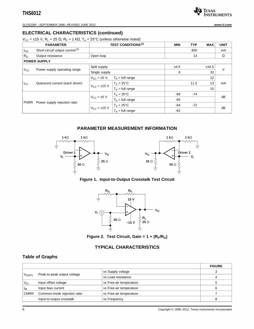
IOS Short-circuit output current (2) 800 mA
RO Output resistance Open loop 13 ΩPOWER SUPPLY
Split supply ±4.5 ±16.5VCC Power supply operating range V
Single supply 9 33
VCC = ±5 V, TA = full range 12
ICC Quiescent current (each driver) TA = 25°C 11.5 13 mAVCC = ±15 V
TA = full range 15
TA = 25°C -68 -74VCC = ±5 V dB
TA = full range -65PSRR Power supply rejection ratio
TA = 25°C -64 -72VCC = ±15 V dB
TA = full range -62
PARAMETER MEASUREMENT INFORMATION
Figure 1. Input-to-Output Crosstalk Test Circuit
Figure 2. Test Circuit, Gain = 1 + (RF/RG)
TYPICAL CHARACTERISTICS
Table of Graphs
FIGURE
vs Supply voltage 3VO(PP) Peak-to-peak output voltage
vs Load resistance 4
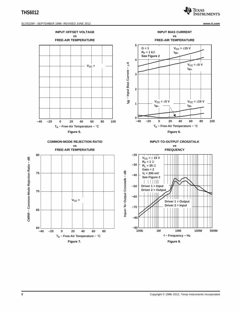
VIO Input offset voltage vs Free-air temperature 5
IIB Input bias current vs Free-air temperature 6
CMRR Common-mode rejection ratio vs Free-air temperature 7
Input-to-output crosstalk vs Frequency 8
6 Copyright © 1998–2012, Texas Instruments Incorporated

VCC − Supply V oltage − V
5 6 7 8 11 12109
0
−5
−10
−15
10
5
TA = 25°CRF = 1 kΩRL = 25 ΩGain = 1
14 1513
15
VO
(PP
)−
Pea
k-to
-Pea
k O
utpu
t Vol
tage
− V
10 100 1000
RL − Load Resistance − Ω
15
5
−5
−15
10
0
−10
VCC = ±15 V
VCC = ±5 V
TA = 25°CRF = 1 kΩGain = 1
VCC = ±5 V
VCC = ±15 VVO
(PP
)−
Pea
k-to
-Pea
k O
utpu
t Vol
tage
− V
THS6012
www.ti.com SLOS226F –SEPTEMBER 1998–REVISED JUNE 2012
TYPICAL CHARACTERISTICS (continued)FIGURE
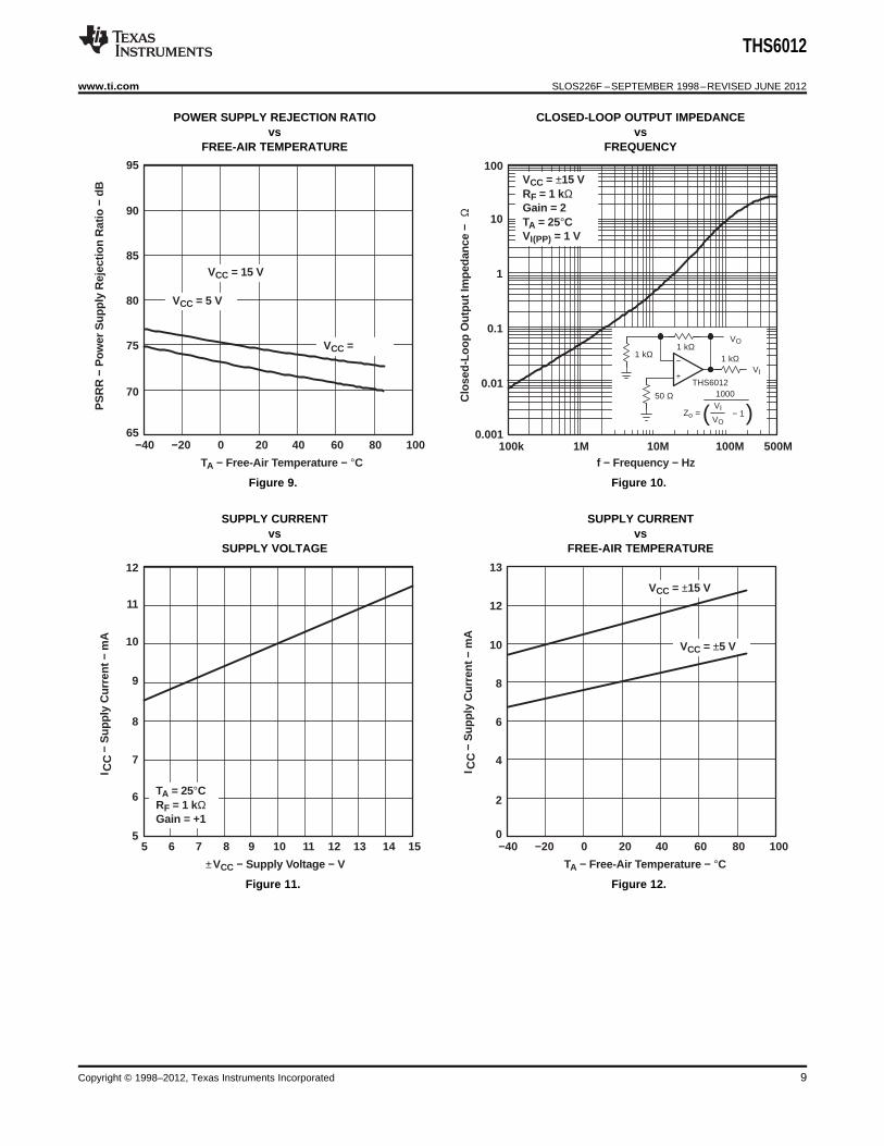
PSRR Power supply rejection ratio vs Free-air temperature 9
Closed-loop output impedance vs Frequency 10
vs Supply voltage 11ICC Supply current
vs Free-air temperature 12
SR Slew rate vs Output step 13, 14
Vn Input voltage noise vs Frequency15
In Input current noise vs Frequency
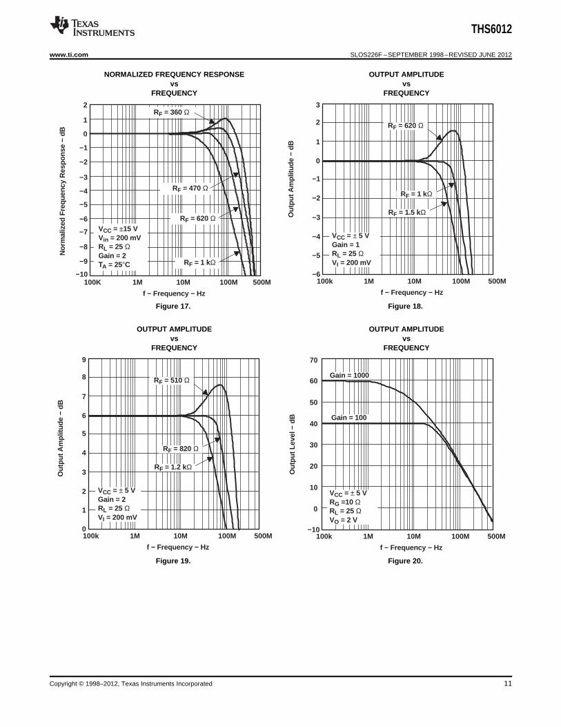
Normalized frequency response vs Frequency 16, 17
Output amplitude vs Frequency 18 - 21
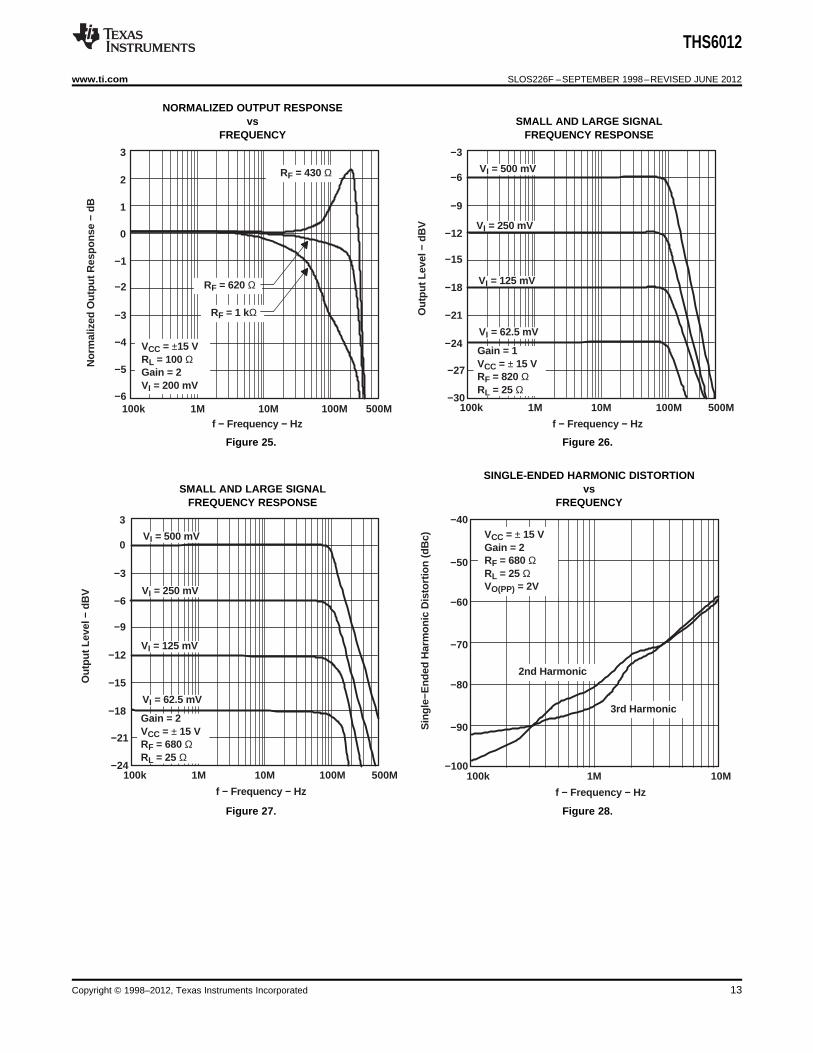
Normalized output response vs Frequency 22 - 25
Small and large frequency response 26, 27
vs Frequency 28, 29Single-ended harmonic distortion
vs Output voltage 30, 31
DC input offset voltage 32, 33Differential gain
Number of 150-Ω loads 34, 35
DC input offset voltage 32, 33Differential phase
Number of 150-Ω loads 34, 35
Output step response 36 - 38
PEAK-TO-PEAK OUTPUT VOLTAGE PEAK-TO-PEAK OUTPUT VOLTAGEvs vs
SUPPLY VOLTAGE LOAD RESISTANCE
Figure 3. Figure 4.
Copyright © 1998–2012, Texas Instruments Incorporated 7
TA − Free-Air T emperature − °C
CM
RR
− C
omm
on-M
ode
Rej
ectio
n R
atio
− d
B
−40 −20 0 20 806040
75
65
60
80
70
VCC = ±5 V
VCC = ±15 V
1 kΩ
1 kΩ
VI +− VO
1 kΩ1 kΩ
f − Frequency − Hz
−80
−9010M100k
−70
−60
500M
Inpu
t−T
o−O
utpu
t Cro
ssta
lk −
dB
−50
−20
1M 100M
VCC = ± 15 VRF = 1 ΩRL = 25 ΩGain = 2VI = 200 mVSee Figure 2
Driver 1 = InputDriver 2 = Output
Driver 1 = OutputDriver 2 = Input
−40
−30
TA − Free-Air T emperature − °C−40 −20 0 20 80 1006040
VCC = ±5 V
VCC = ±15 V
VIO
− In
put O
ffset
Vol
tage
− m
V
1
−1
−3
−5
0
−2
−4
2
G = 1RF = 1 kΩ
TA − Free-Air T emperature − °C−40 −20 0 20 80 1006040
5
3
1
0
4
2
VCC = ±15 VIIB+
VCC = ±5 VIIB+
VCC = ±15 VIIB−
VCC = ±5 VIIB−
I IB−
Inpu
t Bia
s C
urre
nt −
Aµ
G = 1RF = 1 kΩ
THS6012
SLOS226F –SEPTEMBER 1998–REVISED JUNE 2012 www.ti.com
INPUT OFFSET VOLTAGE INPUT BIAS CURRENTvs vs
FREE-AIR TEMPERATURE FREE-AIR TEMPERATURE
Figure 5. Figure 6.
COMMON-MODE REJECTION RATIO INPUT-TO-OUTPUT CROSSTALKvs vs
FREE-AIR TEMPERATURE FREQUENCY
Figure 7. Figure 8.
8 Copyright © 1998–2012, Texas Instruments Incorporated
±VCC − Supply V oltage − V
5 6 7 8 11 12109
6
5
10
8
9
7
I CC
− S
uppl
y C
urre
nt −
mA
TA = 25°CRF = 1 kΩGain = +1
14 1513
12
11
TA − Free-Air T emperature − °C−40 −20 0 20 80 1006040
10
6
2
0
8
4
12
VCC = ±15 V
VCC = ±5 V
I CC
− S
uppl
y C
urre
nt −
mA
13
TA − Free-Air T emperature − °C
PS
RR
− P
ower
Sup
ply
Rej
ectio
n R
atio
− d
B
−40 −20 0 20 80 1006040
90
80
70
65
85
75
95
VCC = 15 V
VCC = 5 V
VCC = −5 V
VCC = −15 V
G = 1RF = 1 kΩ
1
0.1
0.01
0.0011M
f − Frequency − Hz100k 10M 100M
10
100
Clo
sed-
Loop
Out
put I
mpe
danc
e −
VCC = ±15 VRF = 1 kΩGain = 2TA = 25°CVI(PP) = 1 V
500M
Ω
VO
+
−
50 Ω
1 kΩ1 kΩ
VI
THS6012
1 kΩ
( VI
VO=
1000
Zo ) − 1
THS6012
www.ti.com SLOS226F –SEPTEMBER 1998–REVISED JUNE 2012
POWER SUPPLY REJECTION RATIO CLOSED-LOOP OUTPUT IMPEDANCEvs vs
FREE-AIR TEMPERATURE FREQUENCY
Figure 9. Figure 10.
SUPPLY CURRENT SUPPLY CURRENTvs vs
SUPPLY VOLTAGE FREE-AIR TEMPERATURE
Figure 11. Figure 12.
Copyright © 1998–2012, Texas Instruments Incorporated 9

10
1
100VCC = ±15 VTA = 25°C
In+ Noise
f − Frequency − Hz
10 100 1k 10k 100k
nV/
Hz
Hz
− Vo
ltage
Noi
se −
Vn
− C
urre
nt N
oise
− p
A/
I n
10
1
100
In− Noise
Vn Noise
f − Frequency − Hz
Nor
mal
ized
Fre
quen
cy R
espo
nse
− dB
100 1M 10M 100M
−2
−4
−6
−8
−3
−5
−7
2
0
1
−1
VCC = ±15 VVI = 200 mVRL = 25 ΩGain = 1TA = 25°C
RF = 510 Ω
RF = 300 Ω
RF = 750 Ω
RF = 1 kΩ
500M
0
Output Step (Peak−T o−Peak) − V
1500
10020
900
5
1100
700
10
1300
Sle
w R
ate
− V
Sµ
500
300
VCC = ± 15VGain = 5RF = 1 kΩRL = 25 Ω
15
+SR
−SR
0
Output Step (Peak−T o−Peak) − V
1000
1005
700
1
800
600
2 3
900
Sle
w R
ate
− V
Sµ
500
300
4
VCC = ± 5VGain = 2RF = 1 kΩRL = 25 Ω
400
200
+SR
−SR
THS6012
SLOS226F –SEPTEMBER 1998–REVISED JUNE 2012 www.ti.com
SLEW RATE SLEW RATEvs vs
OUTPUT STEP OUTPUT STEP
Figure 13. Figure 14.
INPUT VOLTAGE AND CURRENT NOISE NORMALIZED FREQUENCY RESPONSEvs vs
FREQUENCY FREQUENCY
Figure 15. Figure 16.
10 Copyright © 1998–2012, Texas Instruments Incorporated
f − Frequency − Hz
−1010M100k
20
30
500M
Out
put L
evel
− d
B 40
70
1M 100M
50
60Gain = 1000
0
10VCC = ± 5 VRG =10 ΩRL = 25 ΩVO = 2 V
Gain = 100
f − Frequency − Hz
1
010M100k
4
5
500M
Out
put
Am
plitu
de −
dB
6
9
1M 100M
7
8
2
3
VCC = ± 5 VGain = 2RL = 25 ΩVI = 200 mV
RF = 820 Ω
RF = 1.2 kΩ
RF = 510 Ω
f − Frequency − Hz
Nor
mal
ized
Fre
quen
cy R
espo
nse
− dB
100K 1M 10M 100M
−1
−3
−5
−7
−2
−4
−6
1
2
0
VCC = ±15 VVin = 200 mVRL = 25 ΩGain = 2TA = 25°C
−8
−10
−9
500M
RF = 470 Ω
RF = 360 Ω
RF = 620 Ω
RF = 1 kΩ
f − Frequency − Hz
−5
−610M100k
−2
−1
500MO
utpu
t A
mpl
itude
− d
B
0
3
1M 100M
1
2
−4
−3
VCC = ± 5 VGain = 1RL = 25 ΩVI = 200 mV
RF = 1 kΩ
RF = 1.5 kΩ
RF = 620 Ω
THS6012
www.ti.com SLOS226F –SEPTEMBER 1998–REVISED JUNE 2012
NORMALIZED FREQUENCY RESPONSE OUTPUT AMPLITUDEvs vs
FREQUENCY FREQUENCY
Figure 17. Figure 18.
OUTPUT AMPLITUDE OUTPUT AMPLITUDEvs vs
FREQUENCY FREQUENCY
Figure 19. Figure 20.
Copyright © 1998–2012, Texas Instruments Incorporated 11

1Mf − Frequency − Hz
100k 10M 100M
Nor
mal
ized
Out
put R
espo
nse
− dB
VCC = ±15 VRF = 1 kΩGain = 2VI = 200 mV
500M
−3
−5
−7
−9
−4
−6
−8
−1
0
−2
1
RL = 200 ΩRL = 100 Ω
RL = 50 Ω
RL = 25 Ω
1Mf − Frequency − Hz
100k 10M 100M
Nor
mal
ized
Out
put R
espo
nse
− dB
VCC = ±15 VRL = 100 ΩGain = 1VI = 200 mV
500M
−1
−3
−5
−7
−2
−4
−6
1
2
0
3
RF = 620 Ω
RF = 820 Ω
RF = 1 kΩ
f − Frequency − Hz
−1010M100k
20
30
500M
Out
put L
evel
− d
B 40
70
1M 100M
50
60Gain = 1000
0
10VCC = ± 5 VRG =10 ΩRL = 25 ΩVO = 2 V
Gain = 100
1Mf − Frequency − Hz
100k 10M 100M
Nor
mal
ized
Out
put R
espo
nse
− dB
500M
−3
−5
−7
−9
−4
−6
−8
−1
0
−2
1RL = 200 Ω
RL = 100 Ω
RL = 25 Ω
VCC = ±15 VRF = 1 kΩGain = 1VI = 200 mV
RL = 50 Ω
THS6012
SLOS226F –SEPTEMBER 1998–REVISED JUNE 2012 www.ti.com
OUTPUT AMPLITUDE NORMALIZED OUTPUT RESPONSEvs vs
FREQUENCY FREQUENCY
Figure 21. Figure 22.
NORMALILZED OUTPUT RESPONSE NORMALIZFED OUTPUT RESPONSEvs vs
FREQUENCY FREQUENCY
Figure 23. Figure 24.
12 Copyright © 1998–2012, Texas Instruments Incorporated
f − Frequency − Hz
−90
−1001M
−60
100k
−80
−70
10M
Sin
gle−
End
ed H
arm
onic
Dis
torti
on (d
Bc)
−50
−40
2nd Harmonic
3rd Harmonic
VCC = ± 15 VGain = 2RF = 680 ΩRL = 25 ΩVO(PP) = 2V
f − Frequency − Hz
−21
−2410M100k
−12
−9
500M
Out
put L
evel
− d
BV −6
3
1M 100M
−3
0VI = 500 mV
−18
−15
Gain = 2VCC = ± 15 VRF = 680 ΩRL = 25 Ω
VI = 250 mV
VI = 125 mV
VI = 62.5 mV
1Mf − Frequency − Hz
100k 10M 100M
Nor
mal
ized
Out
put R
espo
nse
− dB
VCC = ±15 VRL = 100 ΩGain = 2VI = 200 mV
500M
−1
−3
−5
−2
−4
−6
1
2
0
3
RF = 430 Ω
RF = 1 kΩ
RF = 620 Ω
f − Frequency − Hz
−27
−3010M100k
−18
−15
500MO
utpu
t Lev
el −
dB
V −12
−3
1M 100M
−9
−6VI = 500 mV
−24
−21
Gain = 1VCC = ± 15 VRF = 820 ΩRL = 25 Ω
VI = 250 mV
VI = 125 mV
VI = 62.5 mV
THS6012
www.ti.com SLOS226F –SEPTEMBER 1998–REVISED JUNE 2012
NORMALIZED OUTPUT RESPONSEvs SMALL AND LARGE SIGNAL
FREQUENCY FREQUENCY RESPONSE
Figure 25. Figure 26.
SINGLE-ENDED HARMONIC DISTORTIONSMALL AND LARGE SIGNAL vs
FREQUENCY RESPONSE FREQUENCY
Figure 27. Figure 28.
Copyright © 1998–2012, Texas Instruments Incorporated 13

VO(PP) − Output V oltage − V
−90
−10020
−80
−70
4
Sin
gle−
End
ed H
arm
onic
Dis
torti
on −
dB
c
−60
−50
1 3
2nd Harmonic
3rd Harmonic
VCC = ± 5 VGain = 2RF = 680 ΩRL = 25 Ωf = 1 MHz
DC Input Offset V oltage − V
0.03
0.02
0.01
0−0.5 −0.1−0.3 0.1 0.7
0.05
−0.7 0.3 0.5
0.04
VCC = ±15 VRL = 150 ΩRF = 1 kΩf = 3.58 MHzGain = 240 IRE Modulation
0.02
0
0.04
Diff
eren
tial P
hase
−°
0.06
0.08
0.10
Phase
Diff
eren
tial G
ain
− %
Gain
f − Frequency − Hz
−90
−1001M
−60
100k
−80
−70
10M
Sin
gle−
End
ed H
arm
onic
Dis
torti
on (d
Bc)
−50
−40
2nd Harmonic
3rd Harmonic
VCC = ± 5 VGain = 2RF = 680 ΩRL = 25 ΩVO(PP) = 2V
VO(PP) − Output V oltage − V
−90
−100100
−80
−70
20
Sin
gle−
End
ed H
arm
onic
Dis
torti
on (d
Bc)
−60
−50
5 15
2nd Harmonic
3rd Harmonic
VCC = ± 15 VGain = 2RF = 680 ΩRL = 25 Ωf = 1 MHz
THS6012
SLOS226F –SEPTEMBER 1998–REVISED JUNE 2012 www.ti.com
SINGLE-ENDED HARMONIC DISTORTION SINGLE-ENDED HARMONIC DISTORTIONvs vs
FREQUENCY OUTPUT VOLTAGE
Figure 29. Figure 30.
SINGLE-ENDED HARMONIC DISTORTION DIFFERENTIAL GAIN AND PHASEvs vs
OUTPUT VOLTAGE DC INPUT OFFSET VOLTAGE
Figure 31. Figure 32.
14 Copyright © 1998–2012, Texas Instruments Incorporated

t − Time − ns
VCC = ±15 VGain = 2RL = 25 ΩRF = 1 kΩtr/tf= 300 psSee Figure 3
100
−100
0
−200VO
− O
utpu
t Vol
tage
− m
V
300
200
0 15010050 200 250 350300 400 450 500
400
−300
−400Number of 150- Ω Loads
0.09
0.06
0.03
0
0.15
Diff
eren
tial G
ain
− %
0.12
0.05
0
0.10
Diff
eren
tial P
hase
−°
0.15
0.20
0.25VCC = ±5 VRF = 1 kΩGain = 2f = 3.58 MHz40 IRE Modulation100 IRE Ramp
Gain
Phase
2 81 43 5 6 7
DC Input Offset V oltage − V
0.03
0.02
0.01
0−0.5 −0.1−0.3 0.1 0.7
0.05
−0.7 0.3 0.5
0.04
VCC = ±5 VRL = 150 ΩRF = 1 kΩf = 3.58 MHzGain = 240 IRE Modulation
0.02
0
0.04
Diff
eren
tial P
hase
−°
0.06
0.08
0.10
Gain
Diff
eren
tial G
ain
− %
Phase
Number of 150- Ω Loads
0.09
0.06
0.03
02 8
0.15
1 4
Diff
eren
tial G
ain
− %
0.12
VCC = ±15 VRF = 1 kΩGain = 2f = 3.58 MHz40 IRE Modulation100 IRE Ramp
0.05
0
0.10
Diff
eren
tial P
hase
−°
0.15
0.20
0.25
Gain
Phase
3 5 6 7
THS6012
www.ti.com SLOS226F –SEPTEMBER 1998–REVISED JUNE 2012
DIFFERENTIAL GAIN AND PHASE DIFFERENTIAL GAIN AND PHASEvs vs
DC INPUT OFFSET VOLTAGE NUMBER OF 150-Ω LOADS
Figure 33. Figure 34.
DIFFERENTIAL GAIN AND PHASEvs
NUMBER OF 150-Ω LOADS 400-mV STEP RESPONSE
Figure 35. Figure 36.
Copyright © 1998–2012, Texas Instruments Incorporated 15

t − Time − ns
2
−2
0
−4VO
− O
utpu
t Vol
tage
− V
6
4
0 15010050 200 250 350300 400 450 500
8
−6
−8
VCC = ±15 VGain = 2RL = 25 ΩRF = 1 kΩtr/tf= 5 nsSee Figure 3
t − Time − ns
VCC = ±15 VGain = 5RL = 25 ΩRF = 2 kΩtr/tf= 5 nsSee Figure 3
4
−4
0
−8VO
− O
utpu
t Vol
tage
− V
12
8
0 15010050 200 250 350300 400 450 500
16
−12
−16
THS6012
SLOS226F –SEPTEMBER 1998–REVISED JUNE 2012 www.ti.com
10-V STEP RESPONSE 20-V STEP RESPONSE
Figure 37. Figure 38.
16 Copyright © 1998–2012, Texas Instruments Incorporated

PD ≅ 2 VCC ICC VCC _ VO
VORL
Where:PD = Power dissipation for one amplifierVCC = Split supply voltageICC = Supply current for that particular amplifierVO = Output voltage of amplifierRL = Load resistance
THS6012
www.ti.com SLOS226F –SEPTEMBER 1998–REVISED JUNE 2012
APPLICATION INFORMATION
The THS6012 contains two independent operational amplifiers. These amplifiers are current feedback topologyamplifiers made for high-speed operation. They have been specifically designed to deliver the full powerrequirements of ADSL and therefore can deliver output currents of at least 400 mA at full output voltage.
The THS6012 is fabricated using Texas Instruments 30-V complementary bipolar process, HVBiCOM. Thisprocess provides excellent isolation and high slew rates that result in the device's excellent crosstalk andextremely low distortion.
INDEPENDENT POWER SUPPLIES
Each amplifier of the THS6012 has its own power supply pins. This was specifically done to solve a problem thatoften occurs when multiple devices in the same package share common power pins. This problem is crosstalkbetween the individual devices caused by currents flowing in common connections. Whenever the currentrequired by one device flows through a common connection shared with another device, this current, inconjunction with the impedance in the shared line, produces an unwanted voltage on the power supply. Properpower supply decoupling and good device power supply rejection helps to reduce this unwanted signal. What isleft is crosstalk.
However, with independent power supply pins for each device, the effects of crosstalk through commonimpedance in the power supplies is more easily managed. This is because it is much easier to achieve lowcommon impedance on the PCB with copper etch than it is to achieve low impedance within the package witheither bond wires or metal traces on silicon.
POWER SUPPLY RESTRICTIONS
Although the THS6012 is specified for operation from power supplies of ±5 V to ±15 V (or singled-ended powersupply operation from 10 V to 30 V), and each amplifier has its own power supply pins, several precautions mustbe taken to assure proper operation.1. The power supplies for each amplifier must be the same value. For example, if the driver 1 uses ±±15 volts,
then the driver 2 must also use ±15 volts. Using ±15 volts for one amplifier and ±5 volts for another amplifieris not allowed.
2. To save power by powering down one of the amplifiers in the package, the following rules must be followed.– The amplifier designated driver 1 must always receive power. This is because the internal startup circuitry
uses the power from the driver 1 device.– The -VCC pins from both drivers must always be at the same potential.– Driver 2 is powered down by simply opening the +VCC connection.
The THS6012 incorporates a standard Class A-B output stage. This means that some of the quiescent current isdirected to the load as the load current increases. So under heavy load conditions, accurate power dissipationcalculations are best achieved through actual measurements. For small loads, however, internal powerdissipation for each amplifier in the THS6012 can be approximated by the following formula:
To find the total THS6012 power dissipation, we simply sum up both amplifier power dissipation results.Generally, the worst case power dissipation occurs when the output voltage is one-half the VCC voltage. One lastnote, which is often overlooked: the feedback resistor (RF) is also a load to the output of the amplifier and shouldbe taken into account for low value feedback resistors.
Copyright © 1998–2012, Texas Instruments Incorporated 17

DIE
Side View (a)
End View (b)
Bottom View (c)
DIE
ThermalPad
THS6012
SLOS226F –SEPTEMBER 1998–REVISED JUNE 2012 www.ti.com
DEVICE PROTECTION FEATURES
The THS6012 has two built-in protection features that protect the device against improper operation. The firstprotection mechanism is output current limiting. Should the output become shorted to ground the output currentis automatically limited to the value given in the data sheet. While this protects the output against excessivecurrent, the device internal power dissipation increases due to the high current and large voltage drop across theoutput transistors. Continuous output shorts are not recommended and could damage the device. Additionally,connection of the amplifier output to one of the supply rails (±VCC) can cause failure of the device and is notrecommended.
The second built-in protection feature is thermal shutdown. Should the internal junction temperature rise aboveapproximately 180°C, the device automatically shuts down. Such a condition could exist with improper heatsinking or if the output is shorted to ground. When the abnormal condition is fixed, the internal thermal shutdowncircuit automatically turns the device back on.
THERMAL INFORMATION
The THS6012 is packaged in a thermally-enhanced DWP package, which is a member of the PowerPAD familyof packages. This package is constructed using a downset leadframe upon which the die is mounted [see Figure39(a) and Figure 39(b)]. This arrangement results in the lead frame being exposed as a thermal pad on theunderside of the package [see Figure 39(c)]. Because this thermal pad has direct thermal contact with the die,excellent thermal performance can be achieved by providing a good thermal path away from the thermal pad.
The PowerPAD package allows for both assembly and thermal management in one manufacturing operation.During the surface-mount solder operation (when the leads are being soldered), the thermal pad can also besoldered to a copper area underneath the package. Through the use of thermal paths within this copper area,heat can be conducted away from the package into either a ground plane or other heat dissipating device. This isdiscussed in more detail in the PCB design considerations section of this document.
The PowerPAD package represents a breakthrough in combining the small area and ease of assembly ofsurface mount with the, heretofore, awkward mechanical methods of heatsinking.
A. The thermal pad is electrically isolated from all terminals in the package.
Figure 39. Views of Thermally Enhanced DWP Package
RECOMMENDED FEEDBACK AND GAIN RESISTOR VALUES
As with all current feedback amplifiers, the bandwidth of the THS6012 is an inversely proportional function of thevalue of the feedback resistor. This can be seen from Figure 17 through Figure 20. The recommended resistorswith a ±15 V power supply for the optimum frequency response with a 25-Ω load system are 680-Ω for a gain = 1and 620-Ω for a gain = 2 or -1. Additionally, using a ±5 V power supply, it is recommended that a 1-kΩ feedbackresistor be used for a gain of 1 and a 820-Ω feedback resistor be used for a gain of 2 or -1. These should beused as a starting point and once optimum values are found, 1% tolerance resistors should be used to maintainfrequency response characteristics. Because there is a finite amount of output resistance of the operationalamplifier, load resistance can play a major part in frequency response. This is especially true with these drivers,which tend to drive low-impedance loads. This can be seen in Figure 11, Figure 23, and Figure 24. As the load
18 Copyright © 1998–2012, Texas Instruments Incorporated
THS6012
www.ti.com SLOS226F –SEPTEMBER 1998–REVISED JUNE 2012
resistance increases, the output resistance of the amplifier becomes less dominant at high frequencies. Tocompensate for this, the feedback resistor should change. For 100-Ω loads, it is recommended that the feedbackresistor be changed to 820 Ω for a gain of 1 and 560 Ω for a gain of 2 or -1. Although, for most applications, afeedback resistor value of 1 kΩ is recommended, which is a good compromise between bandwidth and phasemargin that yields a very stable amplifier.
Consistent with current feedback amplifiers, increasing the gain is best accomplished by changing the gainresistor, not the feedback resistor. This is because the bandwidth of the amplifier is dominated by the feedbackresistor value and internal dominant-pole capacitor. The ability to control the amplifier gain independently of thebandwidth constitutes a major advantage of current feedback amplifiers over conventional voltage feedbackamplifiers. Therefore, once a frequency response is found suitable to a particular application, adjust the value ofthe gain resistor to increase or decrease the overall amplifier gain.
Finally, it is important to realize the effects of the feedback resistance on distortion. Increasing the resistancedecreases the loop gain and increases the distortion. It is also important to know that decreasing load impedanceincreases total harmonic distortion (THD). Typically, the third order harmonic distortion increases more than thesecond order harmonic distortion.
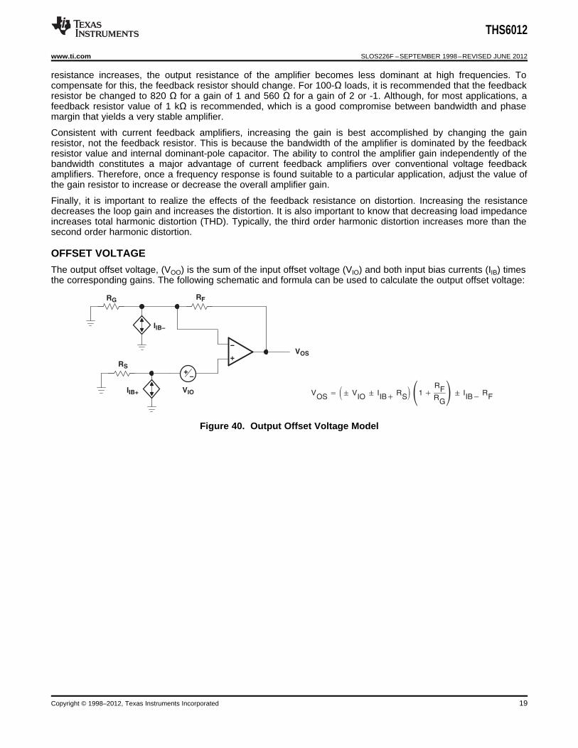
OFFSET VOLTAGE
The output offset voltage, (VOO) is the sum of the input offset voltage (VIO) and both input bias currents (IIB) timesthe corresponding gains. The following schematic and formula can be used to calculate the output offset voltage:
Figure 40. Output Offset Voltage Model
Copyright © 1998–2012, Texas Instruments Incorporated 19
eno eni AV eni1 RFRG (Noninverting Case)
eni en
2 IN RS
2 IN– RF RG2 4 kTRs 4 kTRF RG
Where:
k = Boltzmann’s constant = 1.380658 × 10⁻²³
T = Temperature in degrees Kelvin (273 +°C)RF || RG = Parallel resistance of RF and RG
_+
RF
RS
RG
eRg
eRf
eRs en
IN+
Noiseless
IN–
enieno
THS6012
SLOS226F –SEPTEMBER 1998–REVISED JUNE 2012 www.ti.com
NOISE CALCULATIONS AND NOISE FIGURE
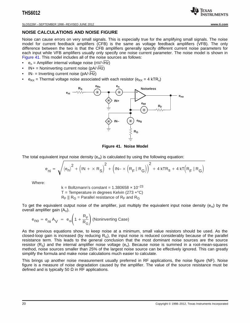
Noise can cause errors on very small signals. This is especially true for the amplifying small signals. The noisemodel for current feedback amplifiers (CFB) is the same as voltage feedback amplifiers (VFB). The onlydifference between the two is that the CFB amplifiers generally specify different current noise parameters foreach input while VFB amplifiers usually only specify one noise current parameter. The noise model is shown inFigure 41. This model includes all of the noise sources as follows:• en = Amplifier internal voltage noise (nV/√Hz)• IN+ = Noninverting current noise (pA/√Hz)• IN- = Inverting current noise (pA/√Hz)• eRX = Thermal voltage noise associated with each resistor (eRX = 4 kTRx)
Figure 41. Noise Model
The total equivalent input noise density (eni) is calculated by using the following equation:
To get the equivalent output noise of the amplifier, just multiply the equivalent input noise density (eni) by theoverall amplifier gain (AV).
As the previous equations show, to keep noise at a minimum, small value resistors should be used. As theclosed-loop gain is increased (by reducing RG), the input noise is reduced considerably because of the parallelresistance term. This leads to the general conclusion that the most dominant noise sources are the sourceresistor (RS) and the internal amplifier noise voltage (en). Because noise is summed in a root-mean-squaresmethod, noise sources smaller than 25% of the largest noise source can be effectively ignored. This can greatlysimplify the formula and make noise calculations much easier to calculate.
This brings up another noise measurement usually preferred in RF applications, the noise figure (NF). Noisefigure is a measure of noise degradation caused by the amplifier. The value of the source resistance must bedefined and is typically 50 Ω in RF applications.
20 Copyright © 1998–2012, Texas Instruments Incorporated
NOISE FIGUREvs
SOURCE RESISTANCE
18
14
0
20
16
12
No
ise
Fig
ure
– d
B
Rs – Source Resistance – Ω10 100 1k 10k
TA = 25°C
8
4
10
6
2
NF 10log
1
en2
IN RS2
4 kTRS
NF 10log
e 2ni
eRs2
THS6012
www.ti.com SLOS226F –SEPTEMBER 1998–REVISED JUNE 2012
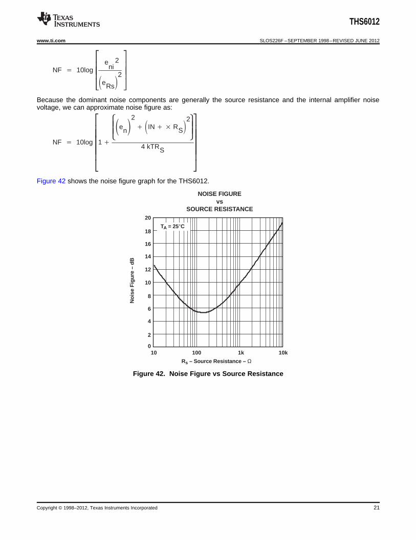
Because the dominant noise components are generally the source resistance and the internal amplifier noisevoltage, we can approximate noise figure as:
Figure 42 shows the noise figure graph for the THS6012.
Figure 42. Noise Figure vs Source Resistance
Copyright © 1998–2012, Texas Instruments Incorporated 21
+
_
THS6012
CLOAD
1 kΩ
Input
Output
1 kΩ
10 Ω
THS6012
SLOS226F –SEPTEMBER 1998–REVISED JUNE 2012 www.ti.com
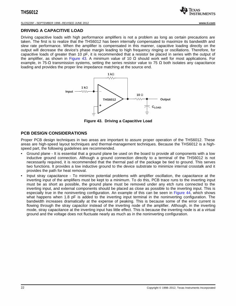
DRIVING A CAPACITIVE LOAD
Driving capacitive loads with high performance amplifiers is not a problem as long as certain precautions aretaken. The first is to realize that the THS6012 has been internally compensated to maximize its bandwidth andslew rate performance. When the amplifier is compensated in this manner, capacitive loading directly on theoutput will decrease the device's phase margin leading to high frequency ringing or oscillations. Therefore, forcapacitive loads of greater than 10 pF, it is recommended that a resistor be placed in series with the output ofthe amplifier, as shown in Figure 43. A minimum value of 10 Ω should work well for most applications. Forexample, in 75-Ω transmission systems, setting the series resistor value to 75 Ω both isolates any capacitanceloading and provides the proper line impedance matching at the source end.
Figure 43. Driving a Capacitive Load
PCB DESIGN CONSIDERATIONS
Proper PCB design techniques in two areas are important to assure proper operation of the THS6012. Theseareas are high-speed layout techniques and thermal-management techniques. Because the THS6012 is a high-speed part, the following guidelines are recommended.• Ground plane - It is essential that a ground plane be used on the board to provide all components with a low
inductive ground connection. Although a ground connection directly to a terminal of the THS6012 is notnecessarily required, it is recommended that the thermal pad of the package be tied to ground. This servestwo functions. It provides a low inductive ground to the device substrate to minimize internal crosstalk and itprovides the path for heat removal.
• Input stray capacitance - To minimize potential problems with amplifier oscillation, the capacitance at theinverting input of the amplifiers must be kept to a minimum. To do this, PCB trace runs to the inverting inputmust be as short as possible, the ground plane must be removed under any etch runs connected to theinverting input, and external components should be placed as close as possible to the inverting input. This isespecially true in the noninverting configuration. An example of this can be seen in Figure 44, which showswhat happens when 1.8 pF is added to the inverting input terminal in the noninverting configuration. Thebandwidth increases dramatically at the expense of peaking. This is because some of the error current isflowing through the stray capacitor instead of the inverting node of the amplifier. Although, in the invertingmode, stray capacitance at the inverting input has little effect. This is because the inverting node is at a virtualground and the voltage does not fluctuate nearly as much as in the noninverting configuration.
22 Copyright © 1998–2012, Texas Instruments Incorporated

f – Frequency – Hz
No
rmal
ized
Fre
qu
ency
Res
po
nse
– d
B
100 1M 10M 100M 500M
–1
–3
–5
–7
–2
–4
–6
3
1
2
0
NORMALIZED FREQUENCY RESPONSEvs
FREQUENCY
VCC = ±15 VVI = 200 mVRL = 25 ΩRF = 1 kΩGain = 1
CI = 0 pF(Stray C Only)
CI = 1.8 pF
+
–
1 kΩ
50 ΩRL =25 Ω
Cin
VinVout
THS6012
www.ti.com SLOS226F –SEPTEMBER 1998–REVISED JUNE 2012
Figure 44. Driver Normalized Frequency Response vs Frequency
• Proper power supply decoupling - Use a minimum of a 6.8-μF tantalum capacitor in parallel with a 0.1-μFceramic capacitor on each supply terminal. It may be possible to share the tantalum among several amplifiersdepending on the application, but a 0.1-μF ceramic capacitor should always be used on the supply terminal ofevery amplifier. In addition, the 0.1-μF capacitor should be placed as close as possible to the supply terminal.As this distance increases, the inductance in the connecting etch makes the capacitor less effective. Thedesigner should strive for distances of less than 0.1 inches between the device power terminal and theceramic capacitors.
Because of its power dissipation, proper thermal management of the THS6012 is required. Although there aremany ways to properly heatsink this device, the following steps illustrate one recommended approach for amultilayer PCB with an internal ground plane.1. Prepare the PCB with a top side etch pattern as shown in Figure 45. There should be etch for the leads as
well as etch for the thermal pad.2. Place 18 holes in the area of the thermal pad. These holes should be 13 mils in diameter. They are kept
small so that solder wicking through the holes is not a problem during reflow.3. It is recommended, but not required, to place six more holes under the package, but outside the thermal pad
area. These holes are 25 mils in diameter. They may be larger because they are not in the area to besoldered so that wicking is not a problem.
4. Connect all 24 holes, the 18 within the thermal pad area and the 6 outside the pad area, to the internalground plane.
5. When connecting these holes to the ground plane, do not use the typical web or spoke via connectionmethodology. Web connections have a high thermal resistance connection that is useful for slowing the heattransfer during soldering operations. This makes the soldering of vias that have plane connections easier.However, in this application, low thermal resistance is desired for the most efficient heat transfer. Therefore,the holes under the THS6012 package should make their connection to the internal ground plane with acomplete connection around the entire circumference of the plated through hole.
6. The top-side solder mask should leave exposed the terminals of the package and the thermal pad area withits five holes. The four larger holes outside the thermal pad area, but still under the package, should becovered with solder mask.
7. Apply solder paste to the exposed thermal pad area and all of the operational amplifier terminals.8. With these preparatory steps in place, the THS6012 is simply placed in position and run through the solder
Copyright © 1998–2012, Texas Instruments Incorporated 23
PD TMAX–TAJA
Where:
PD = Maximum power dissipation of THS6012 (watts)TMAX = Absolute maximum junction temperature (150°C)TA = Free-ambient air temperature (°C)θJA = θJC + θCA
θJC = Thermal coefficient from junction to case (0.37°C/W)θCA = Thermal coefficient from case to ambient
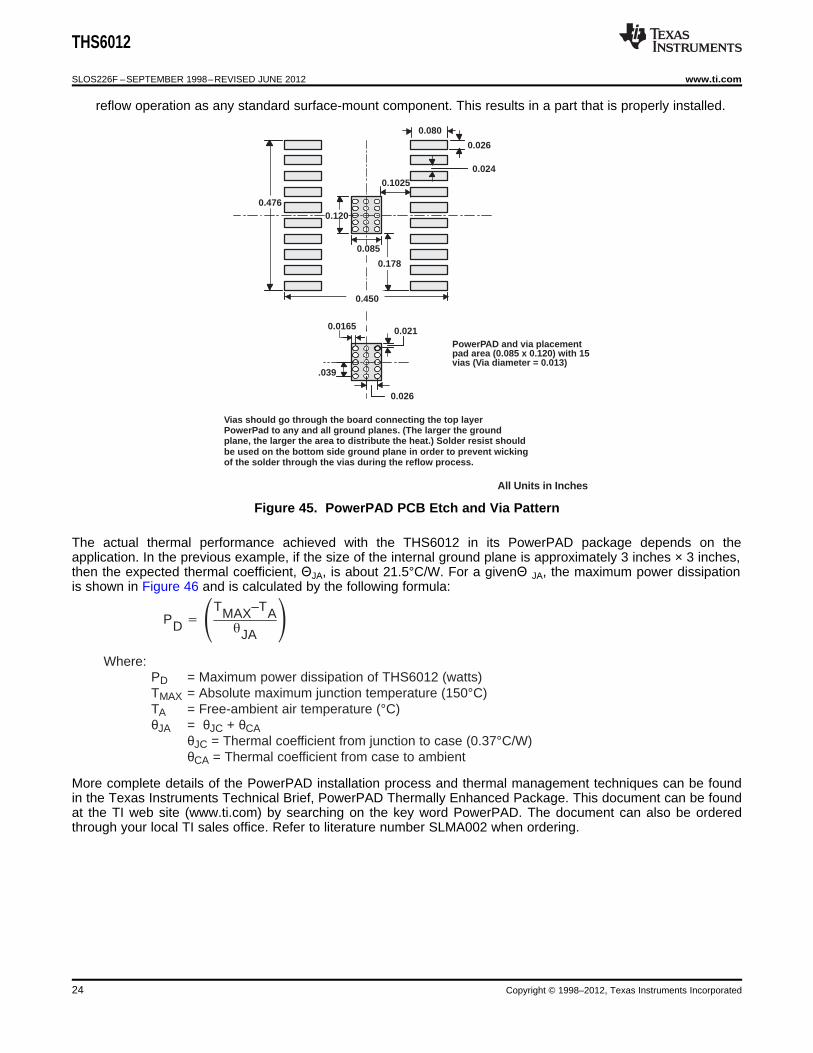
0.1025
0.080
0.178
0.026
0.024
0.0210.0165
0.450
0.476
.039
0.026
0.120
0.085
PowerPAD and via placementpad area (0.085 x 0.120) with 15vias (Via diameter = 0.013)
Vias should go through the board connecting the top layerPowerPad to any and all ground planes. (The larger the groundplane, the larger the area to distribute the heat.) Solder resist shouldbe used on the bottom side ground plane in order to prevent wickingof the solder through the vias during the reflow process.
All Units in Inches
THS6012
SLOS226F –SEPTEMBER 1998–REVISED JUNE 2012 www.ti.com
reflow operation as any standard surface-mount component. This results in a part that is properly installed.
Figure 45. PowerPAD PCB Etch and Via Pattern
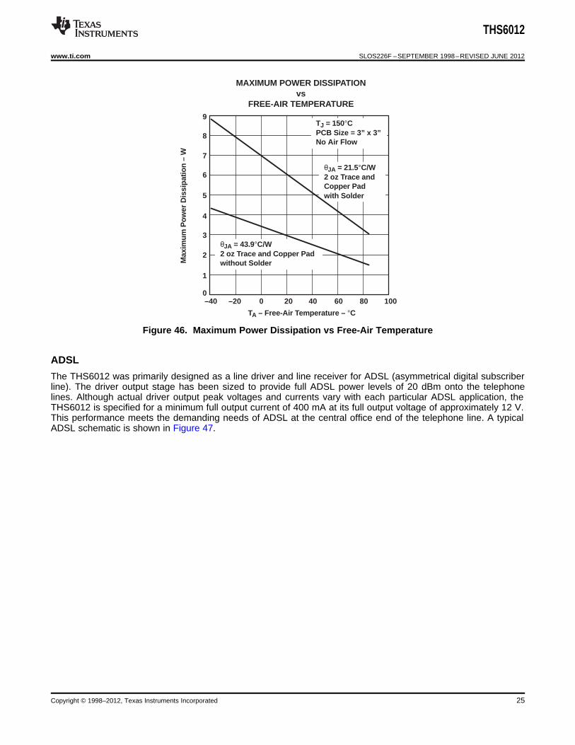
The actual thermal performance achieved with the THS6012 in its PowerPAD package depends on theapplication. In the previous example, if the size of the internal ground plane is approximately 3 inches × 3 inches,then the expected thermal coefficient, ΘJA, is about 21.5°C/W. For a givenΘ JA, the maximum power dissipationis shown in Figure 46 and is calculated by the following formula:
More complete details of the PowerPAD installation process and thermal management techniques can be foundin the Texas Instruments Technical Brief, PowerPAD Thermally Enhanced Package. This document can be foundat the TI web site (www.ti.com) by searching on the key word PowerPAD. The document can also be orderedthrough your local TI sales office. Refer to literature number SLMA002 when ordering.
24 Copyright © 1998–2012, Texas Instruments Incorporated
TA – Free-Air Temperature – °C–40 –20 0 20 80 1006040
MAXIMUM POWER DISSIPATIONvs
FREE-AIR TEMPERATURE
5
3
1
0
4
2
6
7
Max
imu
m P
ow
er D
issi
pat
ion
– W
8
9TJ = 150°CPCB Size = 3” x 3”No Air Flow
θJA = 21.5°C/W2 oz Trace andCopper Padwith Solder
θJA = 43.9°C/W2 oz Trace and Copper Padwithout Solder
THS6012
www.ti.com SLOS226F –SEPTEMBER 1998–REVISED JUNE 2012
Figure 46. Maximum Power Dissipation vs Free-Air Temperature
ADSL
The THS6012 was primarily designed as a line driver and line receiver for ADSL (asymmetrical digital subscriberline). The driver output stage has been sized to provide full ADSL power levels of 20 dBm onto the telephonelines. Although actual driver output peak voltages and currents vary with each particular ADSL application, theTHS6012 is specified for a minimum full output current of 400 mA at its full output voltage of approximately 12 V.This performance meets the demanding needs of ADSL at the central office end of the telephone line. A typicalADSL schematic is shown in Figure 47.
Copyright © 1998–2012, Texas Instruments Incorporated 25

_+
6.8 µF0.1 µF
–15 V
6.8 µF0.1 µF
15 V
1 kΩ1 kΩ
+
+
VI+
_+
6.8 µF0.1 µF
–15 V
6.8 µF0.1 µF
15 V
1 kΩ1 kΩ
+
+
VI–
+
–
1 kΩ
0.1 µF
1 kΩ
2 kΩ
12.5 Ω
+
–
1 kΩ
0.1 µF
1 kΩ
2 kΩ
1:2
Telephone Line
12.5 Ω
–15 V
15 V
15 V
–15 V0.01 µF
THS6062
THS6062
VO+
VO–
THS6012Driver 1
THS6012Driver 2
100 Ω
THS6012
SLOS226F –SEPTEMBER 1998–REVISED JUNE 2012 www.ti.com
Figure 47. THS6012 ADSL Application
The ADSL transmit band consists of 255 separate carrier frequencies each with its own modulation andamplitude level. With such an implementation, it is imperative that signals put onto the telephone line have as lowa distortion as possible. This is because any distortion either interferes directly with other ADSL carrierfrequencies or it creates intermodulation products that interfere with ADSL carrier frequencies.
The THS6012 has been specifically designed for ultra low distortion by careful circuit implementation and bytaking advantage of the superb characteristics of the complementary bipolar process. Driver single-endeddistortion measurements are shown in Figure 28 through Figure 31. It is commonly known that in the differentialdriver configuration, the second order harmonics tend to cancel out. Thus, the dominant total harmonic distortion(THD) will be primarily due to the third order harmonics. For these tests the load was 25 Ω. Additionally,distortion should be reduced as the feedback resistance drops. This is because the bandwidth of the amplifierincreases, which allows the amplifier to react faster to any nonlinearities in the closed-loop system.
Another significant point is the fact that distortion decreases as the impedance load increases. This is becausethe output resistance of the amplifier becomes less significant as compared to the output load resistance.
26 Copyright © 1998–2012, Texas Instruments Incorporated
+
–
C1RF
RG
VOVI
THS6012
VOVI
RFRG
S 1RFC1
S
VI
C2R2R1
C1
RFRG
R1 = R2 = RC1 = C2 = CQ = Peaking Factor(Butterworth Q = 0.707)
(=
1Q
2 – )RG
RF
_+
f–3dB 1
2RC
VIVO
C1
+
–
RG RF
R1
f–3dB 12R1C1
VOVI
1RFRG 1
1 sR1C1
THS6012
www.ti.com SLOS226F –SEPTEMBER 1998–REVISED JUNE 2012
GENERAL CONFIGURATIONS
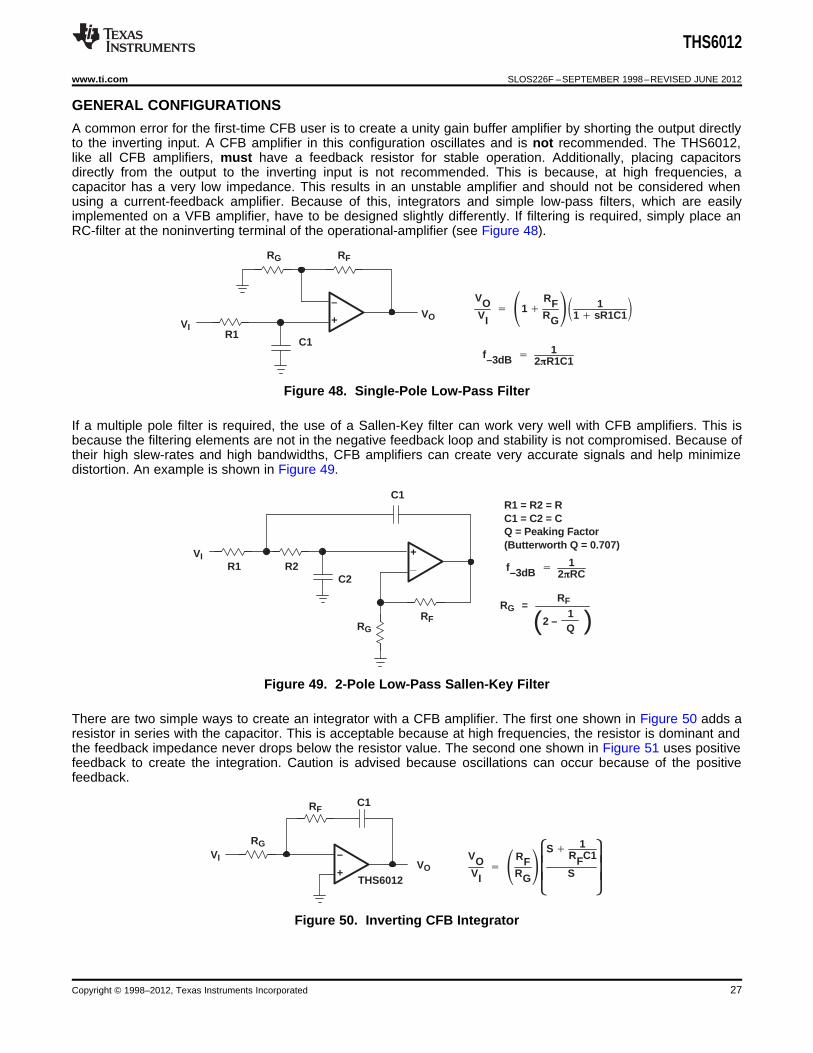
A common error for the first-time CFB user is to create a unity gain buffer amplifier by shorting the output directlyto the inverting input. A CFB amplifier in this configuration oscillates and is not recommended. The THS6012,like all CFB amplifiers, must have a feedback resistor for stable operation. Additionally, placing capacitorsdirectly from the output to the inverting input is not recommended. This is because, at high frequencies, acapacitor has a very low impedance. This results in an unstable amplifier and should not be considered whenusing a current-feedback amplifier. Because of this, integrators and simple low-pass filters, which are easilyimplemented on a VFB amplifier, have to be designed slightly differently. If filtering is required, simply place anRC-filter at the noninverting terminal of the operational-amplifier (see Figure 48).
Figure 48. Single-Pole Low-Pass Filter
If a multiple pole filter is required, the use of a Sallen-Key filter can work very well with CFB amplifiers. This isbecause the filtering elements are not in the negative feedback loop and stability is not compromised. Because oftheir high slew-rates and high bandwidths, CFB amplifiers can create very accurate signals and help minimizedistortion. An example is shown in Figure 49.
Figure 49. 2-Pole Low-Pass Sallen-Key Filter
There are two simple ways to create an integrator with a CFB amplifier. The first one shown in Figure 50 adds aresistor in series with the capacitor. This is acceptable because at high frequencies, the resistor is dominant andthe feedback impedance never drops below the resistor value. The second one shown in Figure 51 uses positivefeedback to create the integration. Caution is advised because oscillations can occur because of the positivefeedback.
Figure 50. Inverting CFB Integrator
Copyright © 1998–2012, Texas Instruments Incorporated 27
+
–
620 Ω620 Ω
75 Ω75 Ω
75 Ω
75 Ω
75 Ω
N Lines
VO1
VON
THS6012
75 Ω Transmission Line
VI
+
–
RF
VO
RG
R2R1
C1RA
VI
THS6012
For Stable Operation:
R2
R1 || RA≥
RF
RG
sR1C1( )
RF
RG1 +
VO ≅ VI
THS6012
SLOS226F –SEPTEMBER 1998–REVISED JUNE 2012 www.ti.com
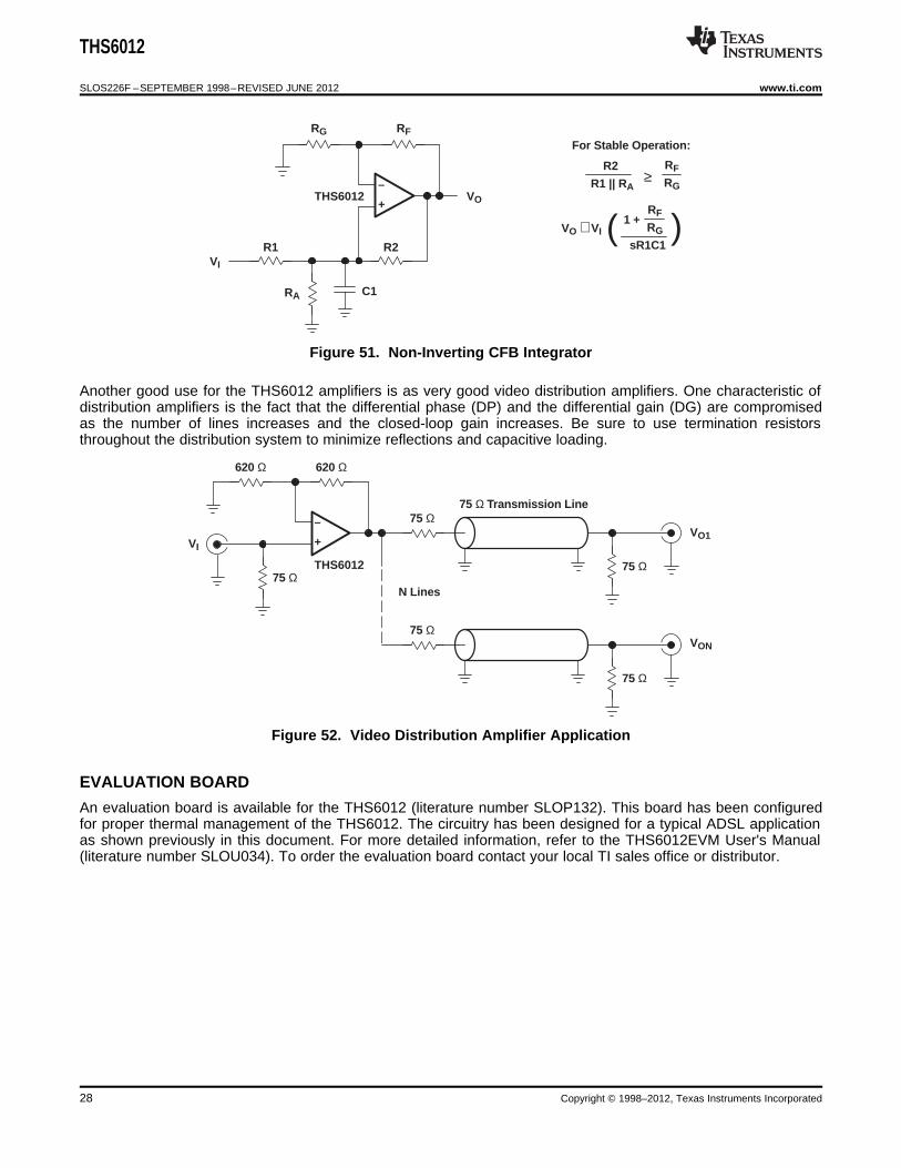
Figure 51. Non-Inverting CFB Integrator
Another good use for the THS6012 amplifiers is as very good video distribution amplifiers. One characteristic ofdistribution amplifiers is the fact that the differential phase (DP) and the differential gain (DG) are compromisedas the number of lines increases and the closed-loop gain increases. Be sure to use termination resistorsthroughout the distribution system to minimize reflections and capacitive loading.
Figure 52. Video Distribution Amplifier Application
EVALUATION BOARD
An evaluation board is available for the THS6012 (literature number SLOP132). This board has been configuredfor proper thermal management of the THS6012. The circuitry has been designed for a typical ADSL applicationas shown previously in this document. For more detailed information, refer to the THS6012EVM User's Manual(literature number SLOU034). To order the evaluation board contact your local TI sales office or distributor.
28 Copyright © 1998–2012, Texas Instruments Incorporated

PACKAGE OPTION ADDENDUM
www.ti.com 10-Dec-2020
Addendum-Page 1
PACKAGING INFORMATION
Orderable Device Status(1)
Package Type PackageDrawing
Pins PackageQty
Eco Plan(2)
Lead finish/Ball material
(6)
MSL Peak Temp(3)
Op Temp (°C) Device Marking(4/5)
Samples
THS6012CDWP ACTIVE SO PowerPAD DWP 20 25 RoHS & Green NIPDAU Level-2-260C-1 YEAR 0 to 70 THS6012C
THS6012CDWPR ACTIVE SO PowerPAD DWP 20 2000 RoHS & Green NIPDAU Level-2-260C-1 YEAR 0 to 70 THS6012C
THS6012IDWP ACTIVE SO PowerPAD DWP 20 25 RoHS & Green NIPDAU Level-2-260C-1 YEAR -40 to 85 THS6012I
THS6012IDWPR ACTIVE SO PowerPAD DWP 20 2000 RoHS & Green NIPDAU Level-2-260C-1 YEAR -40 to 85 THS6012I
(1) The marketing status values are defined as follows:ACTIVE: Product device recommended for new designs.LIFEBUY: TI has announced that the device will be discontinued, and a lifetime-buy period is in effect.NRND: Not recommended for new designs. Device is in production to support existing customers, but TI does not recommend using this part in a new design.PREVIEW: Device has been announced but is not in production. Samples may or may not be available.OBSOLETE: TI has discontinued the production of the device.
(2) RoHS: TI defines "RoHS" to mean semiconductor products that are compliant with the current EU RoHS requirements for all 10 RoHS substances, including the requirement that RoHS substancedo not exceed 0.1% by weight in homogeneous materials. Where designed to be soldered at high temperatures, "RoHS" products are suitable for use in specified lead-free processes. TI mayreference these types of products as "Pb-Free".RoHS Exempt: TI defines "RoHS Exempt" to mean products that contain lead but are compliant with EU RoHS pursuant to a specific EU RoHS exemption.Green: TI defines "Green" to mean the content of Chlorine (Cl) and Bromine (Br) based flame retardants meet JS709B low halogen requirements of <=1000ppm threshold. Antimony trioxide basedflame retardants must also meet the <=1000ppm threshold requirement.
(3) MSL, Peak Temp. - The Moisture Sensitivity Level rating according to the JEDEC industry standard classifications, and peak solder temperature.
(4) There may be additional marking, which relates to the logo, the lot trace code information, or the environmental category on the device.
(5) Multiple Device Markings will be inside parentheses. Only one Device Marking contained in parentheses and separated by a "~" will appear on a device. If a line is indented then it is a continuationof the previous line and the two combined represent the entire Device Marking for that device.
(6) Lead finish/Ball material - Orderable Devices may have multiple material finish options. Finish options are separated by a vertical ruled line. Lead finish/Ball material values may wrap to twolines if the finish value exceeds the maximum column width.
Important Information and Disclaimer:The information provided on this page represents TI's knowledge and belief as of the date that it is provided. TI bases its knowledge and belief on informationprovided by third parties, and makes no representation or warranty as to the accuracy of such information. Efforts are underway to better integrate information from third parties. TI has taken and
PACKAGE OPTION ADDENDUM
www.ti.com 10-Dec-2020
Addendum-Page 2
continues to take reasonable steps to provide representative and accurate information but may not have conducted destructive testing or chemical analysis on incoming materials and chemicals.TI and TI suppliers consider certain information to be proprietary, and thus CAS numbers and other limited information may not be available for release.
In no event shall TI's liability arising out of such information exceed the total purchase price of the TI part(s) at issue in this document sold by TI to Customer on an annual basis.

TAPE AND REEL INFORMATION
*All dimensions are nominal
Device PackageType
PackageDrawing
Pins SPQ ReelDiameter
(mm)
ReelWidth
W1 (mm)
A0(mm)
B0(mm)
K0(mm)
P1(mm)
W(mm)
Pin1Quadrant
THS6012CDWPR SOPower PAD
DWP 20 2000 330.0 24.4 10.8 13.3 2.7 12.0 24.0 Q1
THS6012IDWPR SOPower PAD
DWP 20 2000 330.0 24.4 10.8 13.3 2.7 12.0 24.0 Q1
PACKAGE MATERIALS INFORMATION
www.ti.com 5-Jan-2022
Pack Materials-Page 1

*All dimensions are nominal
Device Package Type Package Drawing Pins SPQ Length (mm) Width (mm) Height (mm)
THS6012CDWPR SO PowerPAD DWP 20 2000 350.0 350.0 43.0
THS6012IDWPR SO PowerPAD DWP 20 2000 350.0 350.0 43.0
PACKAGE MATERIALS INFORMATION
www.ti.com 5-Jan-2022
Pack Materials-Page 2
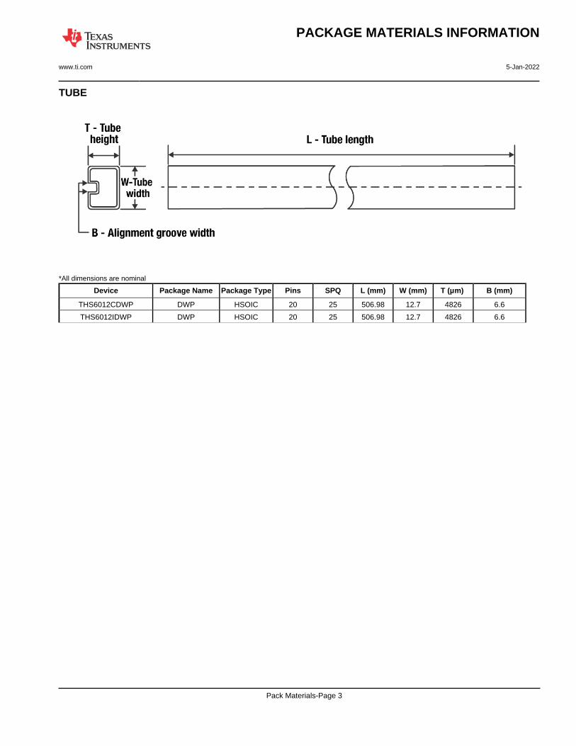
TUBE
*All dimensions are nominal
Device Package Name Package Type Pins SPQ L (mm) W (mm) T (µm) B (mm)
THS6012CDWP DWP HSOIC 20 25 506.98 12.7 4826 6.6
THS6012IDWP DWP HSOIC 20 25 506.98 12.7 4826 6.6
PACKAGE MATERIALS INFORMATION
www.ti.com 5-Jan-2022
Pack Materials-Page 3


IMPORTANT NOTICE AND DISCLAIMERTI PROVIDES TECHNICAL AND RELIABILITY DATA (INCLUDING DATA SHEETS), DESIGN RESOURCES (INCLUDING REFERENCE DESIGNS), APPLICATION OR OTHER DESIGN ADVICE, WEB TOOLS, SAFETY INFORMATION, AND OTHER RESOURCES “AS IS” AND WITH ALL FAULTS, AND DISCLAIMS ALL WARRANTIES, EXPRESS AND IMPLIED, INCLUDING WITHOUT LIMITATION ANY IMPLIED WARRANTIES OF MERCHANTABILITY, FITNESS FOR A PARTICULAR PURPOSE OR NON-INFRINGEMENT OF THIRD PARTY INTELLECTUAL PROPERTY RIGHTS.These resources are intended for skilled developers designing with TI products. You are solely responsible for (1) selecting the appropriate TI products for your application, (2) designing, validating and testing your application, and (3) ensuring your application meets applicable standards, and any other safety, security, regulatory or other requirements.These resources are subject to change without notice. TI grants you permission to use these resources only for development of an application that uses the TI products described in the resource. Other reproduction and display of these resources is prohibited. No license is granted to any other TI intellectual property right or to any third party intellectual property right. TI disclaims responsibility for, and you will fully indemnify TI and its representatives against, any claims, damages, costs, losses, and liabilities arising out of your use of these resources.TI’s products are provided subject to TI’s Terms of Sale or other applicable terms available either on ti.com or provided in conjunction with such TI products. TI’s provision of these resources does not expand or otherwise alter TI’s applicable warranties or warranty disclaimers for TI products.TI objects to and rejects any additional or different terms you may have proposed. IMPORTANT NOTICE
Mailing Address: Texas Instruments, Post Office Box 655303, Dallas, Texas 75265Copyright © 2022, Texas Instruments Incorporated