4 × 12-bit and 4 × 16-bit octal dac with on-chip reference …€¦ · 4 × 12-bit and 4 ×...
TRANSCRIPT

4 × 12-Bit and 4 × 16-Bit Octal DAC with On-Chip Reference in 14-Lead TSSOP
AD5678
Rev. C Information furnished by Analog Devices is believed to be accurate and reliable. However, no responsibility is assumed by Analog Devices for its use, nor for any infringements of patents or other rights of third parties that may result from its use. Specifications subject to change without notice. No license is granted by implication or otherwise under any patent or patent rights of Analog Devices. Trademarks and registered trademarks are the property of their respective owners.
One Technology Way, P.O. Box 9106, Norwood, MA 02062-9106, U.S.A.Tel: 781.329.4700 www.analog.com Fax: 781.461.3113 ©2005–2011 Analog Devices, Inc. All rights reserved.
FEATURES Low power octal DAC with
Four 16-bit DACs Four 12-bit DACs
14-lead/16-lead TSSOP On-chip 1.25 V/2.5 V, 5 ppm/°C reference Power down to 400 nA @ 5 V, 200 nA @ 3 V 2.7 V to 5.5 V power supply Guaranteed monotonic by design Power-on reset to zero scale 3 power-down functions Hardware LDAC and LDAC override function
CLR function to programmable code
Rail-to-rail operation
APPLICATIONS Process control Data acquisition systems Portable battery-powered instruments Digital gain and offset adjustment Programmable voltage current sources Programmable attenuators
FUNCTIONAL BLOCK DIAGRAM
INTERFACELOGIC
INPUTREGISTER
DIN
LDAC
GND
VOUTH
VDD
LDAC1
VREFIN/VREFOUT
SYNC
SCLK
AD5678
CLR1
1RU-16 PACKAGE ONLY
1.25V/2.5VREF
VOUTA
VOUTB
VOUTC
VOUTD
VOUTE
VOUTF
VOUTG
DACREGISTER
STRINGDAC A
BUFFER
INPUTREGISTER
DACREGISTER
STRINGDAC B
BUFFER
INPUTREGISTER
DACREGISTER
STRINGDAC C
BUFFER
INPUTREGISTER
DACREGISTER
STRINGDAC D
BUFFER
INPUTREGISTER
DACREGISTER
STRINGDAC E
BUFFER
INPUTREGISTER
DACREGISTER
STRINGDAC F
BUFFER
INPUTREGISTER
DACREGISTER
STRINGDAC G
BUFFER
INPUTREGISTER
DACREGISTER
STRINGDAC H
BUFFER
POWER-DOWNLOGIC
POWER-ONRESET
0529
9-00
1
Figure 1.
GENERAL DESCRIPTION
The AD5678 is a low power, octal, buffered voltage-output DAC with four 12-bit DACs and four 16-bit DACs in a single package. All devices operate from a single 2.7 V to 5.5 V supply and are guaranteed monotonic by design.
The AD5678 has an on-chip reference with an internal gain of 2. The AD5678-1 has a 1.25 V 5 ppm/°C reference, giving a full-scale output of 2.5 V; the AD5678-2 has a 2.5 V 5 ppm/°C reference, giving a full-scale output of 5 V. The on-board reference is off at power-up, allowing the use of an external reference. The internal reference is enabled via a software write.
The part incorporates a power-on reset circuit that ensures that the DAC output powers up to 0 V and remains powered up at this level until a valid write takes place. The part contains a power-down feature that reduces the current consumption of the device to 400 nA at 5 V and provides software-selectable output loads while in power-down mode for any or all DAC channels.
The outputs of all DACs can be updated simultaneously using the LDAC function, with the added functionality of user-selectable DAC channels to simultaneously update. There is also an asynchronous CLR that clears all DACs to a software-selectable code—0 V, midscale, or full scale.
The AD5678 utilizes a versatile 3-wire serial interface that operates at clock rates of up to 50 MHz and is compatible with standard SPI®, QSPI™, MICROWIRE™, and DSP interface standards. The on-chip precision output amplifier enables rail-to-rail output swing.
PRODUCT HIGHLIGHTS 1. Octal DAC (four 12-bit DACs and four 16-bit DACs). 2. On-chip 1.25 V/2.5 V, 5 ppm/°C reference. 3. Available in 14-lead/16-lead TSSOP. 4. Power-on reset to 0 V. 5. Power-down capability. When powered down, the DAC
typically consumes 200 nA at 3 V and 400 nA at 5 V.

AD5678
Rev. C | Page 2 of 28
TABLE OF CONTENTS Features .............................................................................................. 1
Applications....................................................................................... 1
Functional Block Diagram .............................................................. 1
General Description ......................................................................... 1
Product Highlights ........................................................................... 1
Revision History ............................................................................... 2
Specifications..................................................................................... 3
AC Characteristics........................................................................ 7
Timing Characteristics ................................................................ 8
Absolute Maximum Ratings............................................................ 9
ESD Caution.................................................................................. 9
Pin Configuration and Function Descriptions........................... 10
Typical Performance Characteristics ........................................... 11
Terminology .................................................................................... 18
Theory of Operation ...................................................................... 20
D/A Section................................................................................. 20
Resistor String............................................................................. 20
Internal Reference ...................................................................... 20
Output Amplifier........................................................................ 21
Serial Interface ............................................................................ 21
Input Shift Register .................................................................... 22
SYNC Interrupt .......................................................................... 22
Internal Reference Register ....................................................... 23
Power-On Reset .......................................................................... 23
Power-Down Modes .................................................................. 23
Clear Code Register ................................................................... 23
LDAC Function .......................................................................... 25
Power Supply Bypassing and Grounding................................ 25
Outline Dimensions ....................................................................... 26
Ordering Guide .......................................................................... 26
REVISION HISTORY
2/11—Rev. B to Rev. C Changes to Zero-Code Error Parameter and Offset Error Parameter, Table 1............................................................................. 3 Changes to Zero-Code Error Parameter and Offset Error Parameter, Table 2............................................................................. 5
2/09—Rev. A to Rev. B Changes to Reference Current Parameter, Table 1....................... 3 Change to IDD (Normal Mode) Parameter, Table 1 ...................... 4 Changes to Reference Current Parameter, Table 2....................... 5 Change to IDD (Normal Mode) Parameter, Table 2 ...................... 6
11/05—Rev. 0 to Rev. A Change to General Description ...................................................... 1 Change to Specifications.................................................................. 3 Replaced Figure 48 ......................................................................... 22 Change to the Power-Down Modes Section ............................... 23
10/05—Revision 0: Initial Version

AD5678
Rev. C | Page 3 of 28
SPECIFICATIONS VDD = 4.5 V to 5.5 V, RL = 2 kΩ to GND, CL = 200 pF to GND, VREFIN = VDD. All specifications TMIN to TMAX, unless otherwise noted.
Table 1. A Grade1 B Grade1 Parameter Min Typ Max Min Typ Max Unit Conditions/Comments STATIC PERFORMANCE2
AD5678 (DAC C, D, E, F) Resolution 12 12 Bits Relative Accuracy ±0.5 ±2 ±0.5 ±1 LSB See Figure 11 Differential Nonlinearity ±0.25 ±0.25 LSB Guaranteed monotonic by design
(see Figure 12) AD5678 (DAC A, B, G, H)
Resolution 16 16 Bits Relative Accuracy ±8 ±32 ±8 ±16 LSB See Figure 5 Differential Nonlinearity ±1 ±1 LSB Guaranteed monotonic by design (see Figure 6)
Zero-Code Error 6 19 6 19 mV All 0s loaded to DAC register (see Figure 17) Zero-Code Error Drift ±2 ±2 μV/°C Full-Scale Error −0.2 −1 −0.2 −1 % FSR All 1s loaded to DAC register (see Figure 18) Gain Error ±1 ±1 % FSR Gain Temperature
Coefficient ±2.5 ±2.5 ppm Of FSR/°C
Offset Error ±6 ±19 ±6 ±19 mV DC Power Supply Rejection
Ratio –80 –80 dB VDD ± 10%
DC Crosstalk (External Reference)
10 10 μV Due to full-scale output change, RL = 2 kΩ to GND or VDD
5 5 μV/mA Due to load current change 10 10 μV Due to powering down (per channel) DC Crosstalk
(Internal Reference) 25 25 μV Due to full-scale output change,
RL = 2 kΩ to GND or VDD 10 10 μV/mA Due to load current change
OUTPUT CHARACTERISTICS3 Output Voltage Range 0 VDD 0 VDD V Capacitive Load Stability 2 2 nF RL = ∞ 10 10 nF RL = 2 kΩ DC Output Impedance 0.5 0.5 Ω Short-Circuit Current 30 30 mA VDD = 5 V Power-Up Time 4 4 μs Coming out of power-down mode; VDD = 5 V
REFERENCE INPUTS Reference Input Voltage VDD VDD V ±1% for specified performance Reference Current 35 55 35 55 μA VREF = VDD = 5.5 V (per DAC channel) Reference Input Range 0 VDD 0 VDD V Reference Input Impedance 14.6 14.6 kΩ Per DAC channel
REFERENCE OUTPUT Output Voltage
AD5678-2 2.495 2.505 2.495 2.505 V At ambient Reference TC3 ±5 ±10 ±5 ±10 ppm/°C Reference Output Impedance 7.5 7.5 kΩ
LOGIC INPUTS3 Input Current ±3 ±3 μA All digital inputs Input Low Voltage, VINL 0.8 0.8 V VDD = 5 V Input High Voltage, VINH 2 2 V VDD = 5 V Pin Capacitance 3 3 pF
AD5678
Rev. C | Page 4 of 28
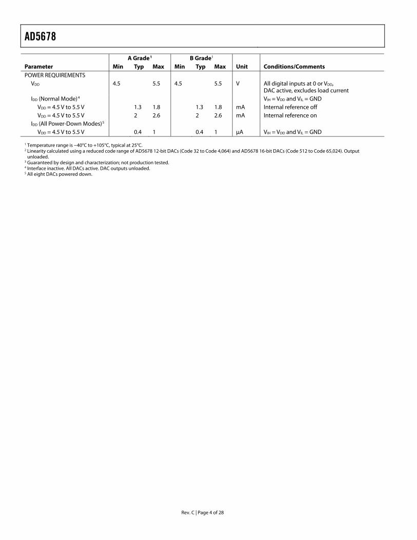
A Grade1 B Grade1 Parameter Min Typ Max Min Typ Max Unit Conditions/Comments POWER REQUIREMENTS
VDD 4.5 5.5 4.5 5.5 V All digital inputs at 0 or VDD, DAC active, excludes load current
IDD (Normal Mode)4 VIH = VDD and VIL = GND VDD = 4.5 V to 5.5 V 1.3 1.8 1.3 1.8 mA Internal reference off VDD = 4.5 V to 5.5 V 2 2.6 2 2.6 mA Internal reference on
IDD (All Power-Down Modes)5 VDD = 4.5 V to 5.5 V 0.4 1 0.4 1 μA VIH = VDD and VIL = GND
1 Temperature range is −40°C to +105°C, typical at 25°C. 2 Linearity calculated using a reduced code range of AD5678 12-bit DACs (Code 32 to Code 4,064) and AD5678 16-bit DACs (Code 512 to Code 65,024). Output
unloaded. 3 Guaranteed by design and characterization; not production tested. 4 Interface inactive. All DACs active. DAC outputs unloaded. 5 All eight DACs powered down.
AD5678
Rev. C | Page 5 of 28
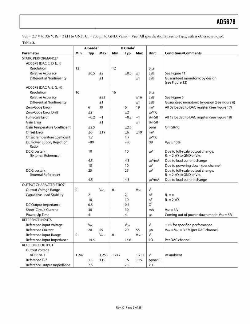
VDD = 2.7 V to 3.6 V, RL = 2 kΩ to GND, CL = 200 pF to GND, VREFIN = VDD. All specifications TMIN to TMAX, unless otherwise noted.
Table 2. A Grade1 B Grade1 Parameter Min Typ Max Min Typ Max Unit Conditions/Comments STATIC PERFORMANCE2
AD5678 (DAC C, D, E, F) Resolution 12 12 Bits Relative Accuracy ±0.5 ±2 ±0.5 ±1 LSB See Figure 11 Differential Nonlinearity ±1 ±1 LSB Guaranteed monotonic by design
(see Figure 12) AD5678 (DAC A, B, G, H)
Resolution 16 16 Bits Relative Accuracy ±32 ±16 LSB See Figure 5 Differential Nonlinearity ±1 ±1 LSB Guaranteed monotonic by design (See Figure 6)
Zero-Code Error 6 19 6 19 mV All 0s loaded to DAC register (See Figure 17) Zero-Code Error Drift ±2 ±2 μV/°C Full-Scale Error −0.2 −1 −0.2 −1 % FSR All 1s loaded to DAC register (See Figure 18) Gain Error ±1 ±1 % FSR Gain Temperature Coefficient ±2.5 ±2.5 ppm Of FSR/°C Offset Error ±6 ±19 ±6 ±19 mV Offset Temperature Coefficient 1.7 1.7 μV/°C DC Power Supply Rejection
Ratio –80 –80 dB VDD ± 10%
DC Crosstalk (External Reference)
10 10 μV Due to full-scale output change, RL = 2 kΩ to GND or VDD
4.5 4.5 μV/mA Due to load current change 10 10 μV Due to powering down (per channel) DC Crosstalk
(Internal Reference) 25 25 μV Due to full-scale output change,
RL = 2 kΩ to GND or VDD 4.5 4.5 μV/mA Due to load current change
OUTPUT CHARACTERISTICS3 Output Voltage Range 0 VDD 0 VDD V Capacitive Load Stability 2 2 nF RL = ∞ 10 10 nF RL = 2 kΩ DC Output Impedance 0.5 0.5 Ω Short-Circuit Current 30 30 mA VDD = 3 V Power-Up Time 4 4 μs Coming out of power-down mode; VDD = 3 V
REFERENCE INPUTS Reference Input Voltage VDD VDD V ±1% for specified performance Reference Current 20 55 20 55 μA VREF = VDD = 3.6 V (per DAC channel) Reference Input Range 0 VDD 0 VDD V Reference Input Impedance 14.6 14.6 kΩ Per DAC channel
REFERENCE OUTPUT Output Voltage
AD5678-1 1.247 1.253 1.247 1.253 V At ambient Reference TC3 ±5 ±15 ±5 ±15 ppm/°C Reference Output Impedance 7.5 7.5 kΩ

AD5678
Rev. C | Page 6 of 28
A Grade1 B Grade1 Parameter Min Typ Max Min Typ Max Unit Conditions/Comments LOGIC INPUTS3
Input Current ±3 ±3 μA All digital inputs Input Low Voltage, VINL 0.8 0.8 V VDD = 3 V Input High Voltage, VINH 2 2 V VDD = 3 V Pin Capacitance 3 3 pF
POWER REQUIREMENTS VDD 2.7 3.6 2.7 3.6 V All digital inputs at 0 or VDD,
DAC active, excludes load current IDD (Normal Mode)4 VIH = VDD and VIL = GND
VDD = 2.7 V to 3.6 V 1.2 1.7 1.2 1.7 mA Internal reference off VDD = 2.7 V to 3.6 V 1.7 2.6 1.7 2.6 mA Internal reference on
IDD (All Power-Down Modes)5 VDD = 2.7 V to 3.6 V 0.2 1 0.2 1 μA VIH = VDD and VIL = GND
1 Temperature range is −40°C to +105°C, typical at 25°C. 2 Linearity calculated using a reduced code range of AD5678 12-bit DACs (Code 32 to Code 4,064) and AD5678 16-bit DACs (Code 512 to Code 65,024). Output
unloaded. 3 Guaranteed by design and characterization; not production tested. 4 Interface inactive. All DACs active. DAC outputs unloaded. 5 All eight DACs powered down.

AD5678
Rev. C | Page 7 of 28
AC CHARACTERISTICS VDD = 2.7 V to 5.5 V, RL = 2 kΩ to GND, CL = 200 pF to GND, VREFIN = VDD. All specifications TMIN to TMAX, unless otherwise noted.
Table 3. Parameter1, 2 Min Typ Max Unit Conditions/Comments3 Output Voltage Settling Time 6 10 μs ¼ to ¾ scale settling to ±2 LSB Slew Rate 1.5 V/μs Digital-to-Analog Glitch Impulse 4 nV-s 1 LSB change around major carry (see Figure 34) Digital Feedthrough 0.1 nV-s Reference Feedthrough −90 dB VREF = 2 V ± 0.1 V p-p, frequency = 10 Hz to 20 MHz Digital Crosstalk 0.5 nV-s Analog Crosstalk 2.5 nV-s DAC-to-DAC Crosstalk 3 nV-s Multiplying Bandwidth 340 kHz VREF = 2 V ± 0.2 V p-p Total Harmonic Distortion −80 dB VREF = 2 V ± 0.1 V p-p, frequency = 10 kHz Output Noise Spectral Density 120 nV/√Hz DAC code = 0x8400, 1 kHz 100 nV/√Hz DAC code = 0x8400, 10 kHz Output Noise 15 μV p-p 0.1 Hz to 10 Hz 1 Guaranteed by design and characterization; not production tested. 2 See the Terminology section. 3 Temperature range is −40°C to +105°C, typical at 25°C.
AD5678
Rev. C | Page 8 of 28
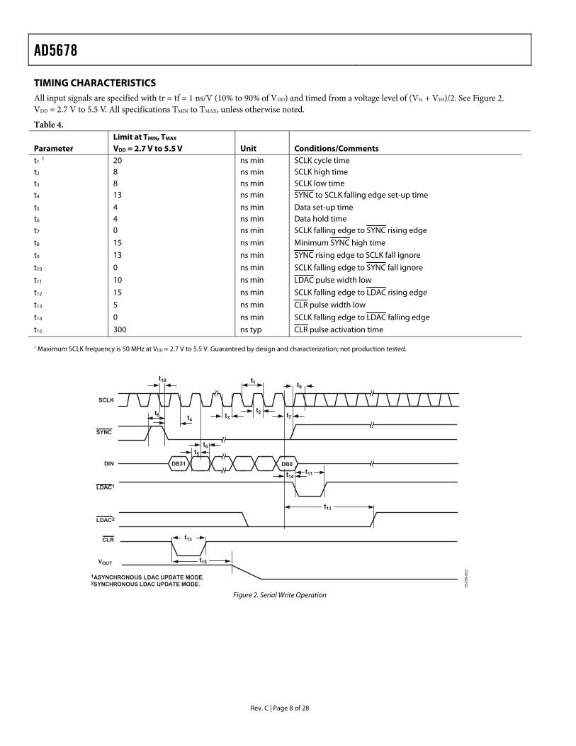
TIMING CHARACTERISTICS All input signals are specified with tr = tf = 1 ns/V (10% to 90% of VDD) and timed from a voltage level of (VIL + VIH)/2. See Figure 2. VDD = 2.7 V to 5.5 V. All specifications TMIN to TMAX, unless otherwise noted.
Table 4. Limit at TMIN, TMAX Parameter VDD = 2.7 V to 5.5 V Unit Conditions/Comments t1 1 20 ns min SCLK cycle time t2 8 ns min SCLK high time t3 8 ns min SCLK low time t4 13 ns min SYNC to SCLK falling edge set-up time
t5 4 ns min Data set-up time t6 4 ns min Data hold time t7 0 ns min SCLK falling edge to SYNC rising edge
t8 15 ns min Minimum SYNC high time
t9 13 ns min SYNC rising edge to SCLK fall ignore
t10 0 ns min SCLK falling edge to SYNC fall ignore
t11 10 ns min LDAC pulse width low
t12 15 ns min SCLK falling edge to LDAC rising edge
t13 5 ns min CLR pulse width low
t14 0 ns min SCLK falling edge to LDAC falling edge
t15 300 ns typ CLR pulse activation time 1 Maximum SCLK frequency is 50 MHz at VDD = 2.7 V to 5.5 V. Guaranteed by design and characterization; not production tested.
0529
9-00
2
t4t3
SCLK
SYNC
DIN
t1
t2
t5
t6
t7t8
DB31
t9t10
t11
t12
t14
1ASYNCHRONOUS LDAC UPDATE MODE.2SYNCHRONOUS LDAC UPDATE MODE.
CLR t13
t15VOUT
DB0
LDAC1
LDAC2
Figure 2. Serial Write Operation

AD5678
Rev. C | Page 9 of 28
ABSOLUTE MAXIMUM RATINGS TA = 25°C, unless otherwise noted.
Table 5. Parameter Rating VDD to GND −0.3 V to +7 V Digital Input Voltage to GND −0.3 V to VDD + 0.3 V VREFIN/VREFOUT to GND −0.3 V to VDD + 0.3 V Operating Temperature Range
Industrial (B Version) −40°C to +105°C Storage Temperature Range −65°C to +150°C Junction Temperature (TJ MAX) 150°C TSSOP Package
Power Dissipation (TJ MAX − TA)/θJA θJA Thermal Impedance 150.4°C/W
Lead Temperature, Soldering SnPb 240°C Pb Free 260°C
Stresses above those listed under Absolute Maximum Ratings may cause permanent damage to the device. This is a stress rating only; functional operation of the device at these or any other conditions above those indicated in the operational section of this specification is not implied. Exposure to absolute maximum rating conditions for extended periods may affect device reliability.
ESD CAUTION ESD (electrostatic discharge) sensitive device. Electrostatic charges as high as 4000 V readily accumulate on the human body and test equipment and can discharge without detection. Although this product features proprietary ESD protection circuitry, permanent damage may occur on devices subjected to high energy electrostatic discharges. Therefore, proper ESD precautions are recommended to avoid performance degradation or loss of functionality.
AD5678
Rev. C | Page 10 of 28
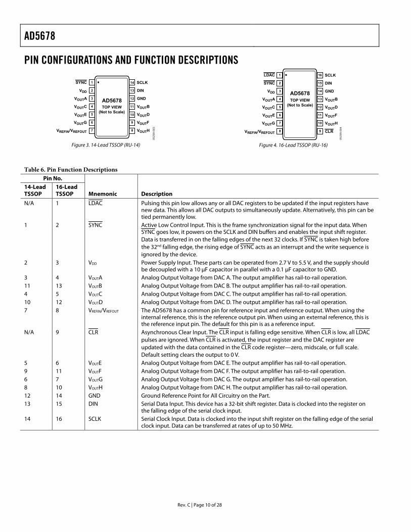
PIN CONFIGURATIONS AND FUNCTION DESCRIPTIONS
0529
9-00
3
1
2
3
4
5
6
7
AD5678
VDD
VOUTA
VOUTC
VREFIN/VREFOUT
VOUTG
VOUTE
14
13
12
11
10
9
8
DIN
GND
VOUTB
VOUTH
VOUTF
VOUTD
SCLK
TOP VIEW(Not to Scale)
SYNC
Figure 3. 14-Lead TSSOP (RU-14)
0529
9-00
4
1
2
3
4
5
6
7
8
16
15
14
13
12
11
10
9
SYNC
VDD
VOUTA
VOUTG
VOUTE
VOUTC
LDAC
DIN
GND
VOUTB
VOUTH
VREFIN/VREFOUT CLR
VOUTF
VOUTD
SCLK
AD5678TOP VIEW
(Not to Scale)
Figure 4. 16-Lead TSSOP (RU-16)
Table 6. Pin Function Descriptions Pin No.
14-Lead TSSOP
16-Lead TSSOP Mnemonic Description
N/A
1
LDAC
Pulsing this pin low allows any or all DAC registers to be updated if the input registers have new data. This allows all DAC outputs to simultaneously update. Alternatively, this pin can be tied permanently low.
1 2 SYNC Active Low Control Input. This is the frame synchronization signal for the input data. When SYNC goes low, it powers on the SCLK and DIN buffers and enables the input shift register. Data is transferred in on the falling edges of the next 32 clocks. If SYNC is taken high before the 32nd falling edge, the rising edge of SYNC acts as an interrupt and the write sequence is ignored by the device.
2 3 VDD Power Supply Input. These parts can be operated from 2.7 V to 5.5 V, and the supply should be decoupled with a 10 μF capacitor in parallel with a 0.1 μF capacitor to GND.
3 4 VOUTA Analog Output Voltage from DAC A. The output amplifier has rail-to-rail operation. 11 13 VOUTB Analog Output Voltage from DAC B. The output amplifier has rail-to-rail operation. 4 5 VOUTC Analog Output Voltage from DAC C. The output amplifier has rail-to-rail operation. 10 12 VOUTD Analog Output Voltage from DAC D. The output amplifier has rail-to-rail operation. 7 8 VREFIN/VREFOUT The AD5678 has a common pin for reference input and reference output. When using the
internal reference, this is the reference output pin. When using an external reference, this is the reference input pin. The default for this pin is as a reference input.
N/A 9 CLR Asynchronous Clear Input. The CLR input is falling edge sensitive. When CLR is low, all LDAC pulses are ignored. When CLR is activated, the input register and the DAC register are updated with the data contained in the CLR code register—zero, midscale, or full scale. Default setting clears the output to 0 V.
5 6 VOUTE Analog Output Voltage from DAC E. The output amplifier has rail-to-rail operation. 9 11 VOUTF Analog Output Voltage from DAC F. The output amplifier has rail-to-rail operation. 6 7 VOUTG Analog Output Voltage from DAC G. The output amplifier has rail-to-rail operation. 8 10 VOUTH Analog Output Voltage from DAC H. The output amplifier has rail-to-rail operation. 12 14 GND Ground Reference Point for All Circuitry on the Part. 13 15 DIN Serial Data Input. This device has a 32-bit shift register. Data is clocked into the register on
the falling edge of the serial clock input. 14 16 SCLK Serial Clock Input. Data is clocked into the input shift register on the falling edge of the serial
clock input. Data can be transferred at rates of up to 50 MHz.
AD5678
Rev. C | Page 11 of 28
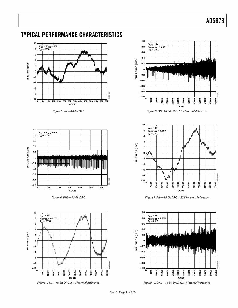
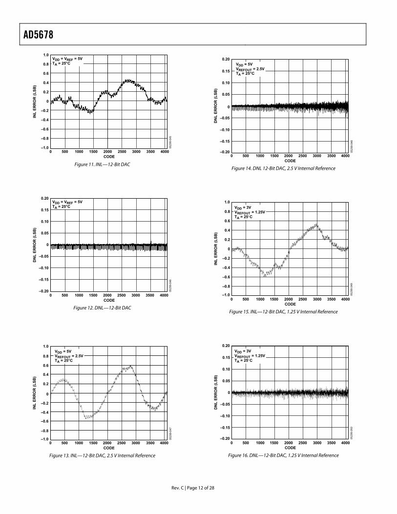
TYPICAL PERFORMANCE CHARACTERISTICS
CODE
INL
ERR
OR
(LSB
)
10
4
6
8
0
2
–6
–10
–8
–2
–4
0 5k 10k 15k 20k 25k 30k 35k 40k 45k 50k 55k 60k 65k
0529
9-01
1
VDD = VREF = 5VTA = 25°C
Figure 5. INL—16-Bit DAC
CODE
DN
L ER
RO
R (L
SB)
1.0
0.6
0.4
0.2
0.8
0
–0.4
–0.2
–0.6
–1.0
–0.8
0 10k 20k 30k 40k 50k 60k
0529
9-01
2
VDD = VREF = 5VTA = 25°C
Figure 6. DNL—16-Bit DAC
CODE
INL
ERR
OR
(LSB
)
10
8
0
–10
–6
–8
–4
6
–2
4
2
6500
0
6000
0
5500
0
5000
0
4500
0
4000
0
3500
0
3000
0
2500
0
2000
0
1500
0
1000
0
50000
VDD = 5VVREFOUT = 2.5VTA = 25°C
0529
9-01
3
Figure 7. INL—16-Bit DAC, 2.5 V Internal Reference
CODE
DN
L ER
RO
R (L
SB)
1.0
0.8
0
–1.0
–0.6
–0.8
–0.4
0.6
–0.2
0.4
0.2
6500
0
6000
0
5500
0
5000
0
4500
0
4000
0
3500
0
3000
0
2500
0
2000
0
1500
0
1000
0
50000
VDD = 5VVREFOUT = 2.5VTA = 25°C
0529
9-01
4
Figure 8. DNL 16-Bit DAC, 2.5 V Internal Reference
CODE
INL
ERR
OR
(LSB
)
10
8
4
6
2
0
–4
–2
–6
–8
–10
6500
0
6000
0
5500
0
5000
0
4500
0
4000
0
3500
0
3000
0
2500
0
2000
0
1500
0
1000
0
50000
0529
9-01
5
VDD = 3VVREFOUT = 1.25VTA = 25°C
Figure 9. INL—16-Bit DAC, 1.25 V Internal Reference
CODE
DN
L ER
RO
R (L
SB)
1.0
0.8
0.4
0.6
0.2
0
–0.4
–0.2
–0.6
–0.8
–1.0
6500
0
6000
0
5500
0
5000
0
4500
0
4000
0
3500
0
3000
0
2500
0
2000
0
1500
0
1000
0
50000
0529
9-01
6VDD = 3VVREFOUT = 1.25VTA = 25°C
Figure 10. DNL—16-Bit DAC, 1.25 V Internal Reference
AD5678
Rev. C | Page 12 of 28
CODE
INL
ERR
OR
(LSB
)
1.0
–1.00 500 1000 1500 2000 2500 3000 3500 4000
0529
9-04
5–0.8
–0.6
–0.4
0
0.4
0.2
–0.2
0.6
0.8VDD = VREF = 5VTA = 25°C
Figure 11. INL—12-Bit DAC
DN
L ER
RO
R (L
SB)
0.20
0.10
0.05
0.15
0
–0.05
–0.10
–0.20
–0.15
0529
9-04
6
CODE0 500 1000 1500 2000 2500 3000 3500 4000
VDD = VREF = 5VTA = 25°C
Figure 12. DNL—12-Bit DAC
CODE
INL
ERR
OR
(LSB
)
1.0
0.8
0
–1.0
–0.8
–0.6
0.6
–0.4
–0.2
0.4
0.2
0 1000500 20001500 350030002500 4000
VDD = 5VVREFOUT = 2.5VTA = 25°C
0529
9-04
7
Figure 13. INL—12-Bit DAC, 2.5 V Internal Reference
CODE
DN
L ER
RO
R (L
SB)
0.20
0.15
0
–0.20
–0.15
–0.10
0.10
–0.05
0.05
0 1000500 20001500 350030002500 4000
VDD = 5VVREFOUT = 2.5VTA = 25°C
0529
9-04
8
Figure 14. DNL 12-Bit DAC, 2.5 V Internal Reference
CODE
INL
ERR
OR
(LSB
)
1.0
–1.00 500 1000 1500 2000 2500 3000 3500 4000
0529
9-04
9
0
0.8
0.6
0.4
0.2
–0.2
–0.4
–0.6
–0.8
VDD = 3VVREFOUT = 1.25VTA = 25°C
Figure 15. INL—12-Bit DAC, 1.25 V Internal Reference
CODE
DN
L ER
RO
R (L
SB)
0.20
–0.200 500 1000 1500 2000 2500 3000 3500 4000
0529
9-05
0
0
0.15
0.10
0.05
–0.05
–0.10
–0.15
VDD = 3VVREFOUT = 1.25VTA = 25°C
Figure 16. DNL—12-Bit DAC, 1.25 V Internal Reference
AD5678
Rev. C | Page 13 of 28
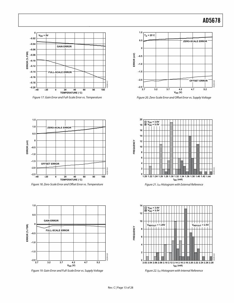
TEMPERATURE (°C)
ERR
OR
(% F
SR)
0
–0.04
–0.02
–0.06
–0.08
–0.10
–0.18
–0.16
–0.14
–0.12
–0.20–40 –20 40200 1008060
0529
9-01
7
VDD = 5V
GAIN ERROR
FULL-SCALE ERROR
Figure 17. Gain Error and Full-Scale Error vs. Temperature
TEMPERATURE (°C)
ERR
OR
(mV)
1.5
1.0
0.5
0
–2.0
–1.5
–1.0
–0.5
–2.5–40 –20 40200 8060 100
0529
9-01
8
OFFSET ERROR
ZERO-SCALE ERROR
Figure 18. Zero-Scale Error and Offset Error vs. Temperature
VDD (V)
ERR
OR
(% F
SR)
1.0
–1.5
–1.0
–0.5
0
0.5
–2.02.7 3.2 3.7 4.74.2 5.2
0529
9-01
9
GAIN ERROR
FULL-SCALE ERROR
Figure 19. Gain Error and Full-Scale Error vs. Supply Voltage
VDD (V)
ERR
OR
(mV)
1.0
0.5
0
–2.0
–1.5
–1.0
–0.5
–2.52.7 3.2 4.23.7 5.24.7
0529
9-02
0
ZERO-SCALE ERROR
OFFSET ERROR
TA = 25°C
Figure 20. Zero-Scale Error and Offset Error vs. Supply Voltage
IDD (mA)
FREQ
UEN
CY
20
01.20 1.22 1.24 1.26 1.28 1.30 1.32 1.34 1.36 1.38 1.40 1.42 1.44
0529
9-02
12
VDD = 3.6VVDD = 5.5V
4
6
8
10
12
14
16
18
Figure 21. IDD Histogram with External Reference
IDD (mA)
FREQ
UEN
CY
14
02.02
0529
9-02
22
4
6
8
10
12
VDD = 3.6VVDD = 5.5V
2.04 2.06 2.08 2.10 2.12 2.14 2.16 2.18 2.20 2.22 2.24 2.26 2.28
VREFOUT = 1.25V VREFOUT = 2.5V
Figure 22. IDD Histogram with Internal Reference
AD5678
Rev. C | Page 14 of 28
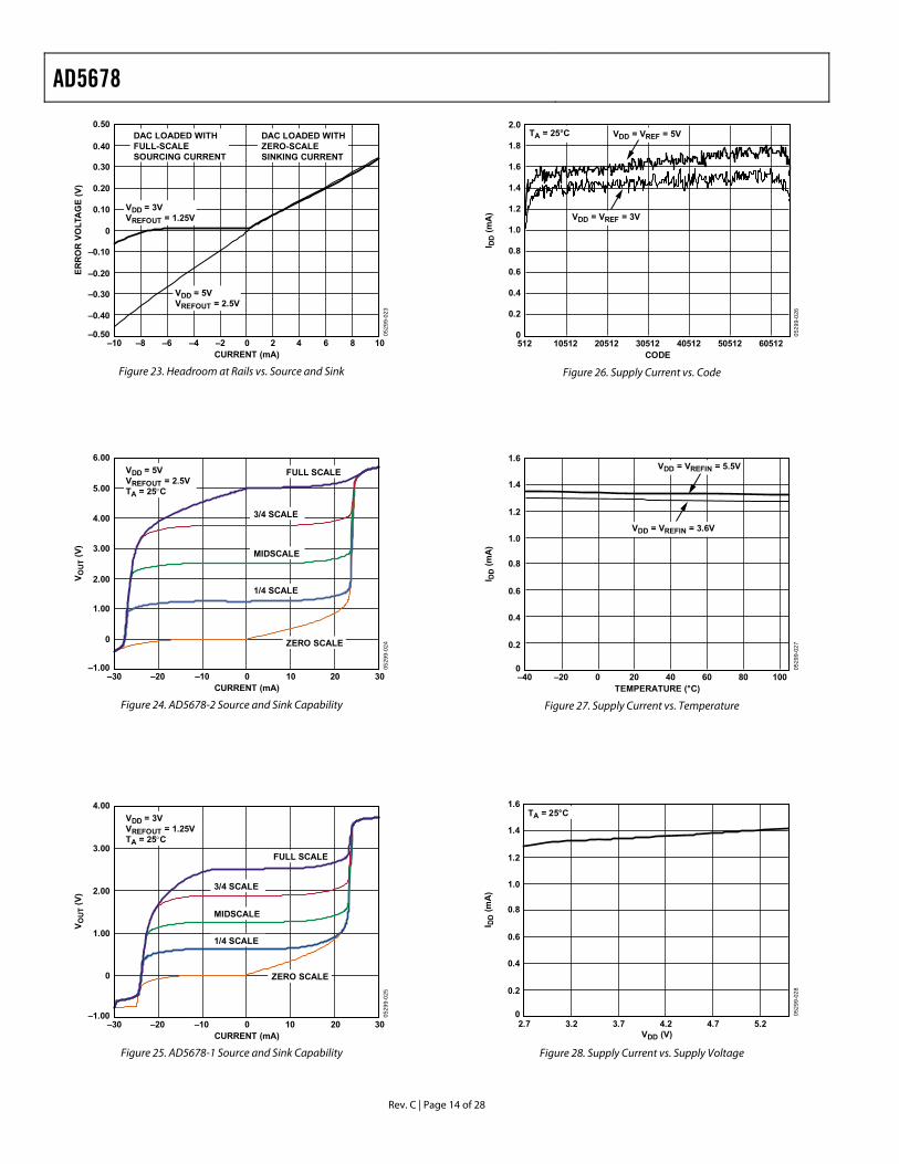
CURRENT (mA)
ERR
OR
VO
LTA
GE
(V)
0.50
0.40
–0.50
–0.40
–0.30
–0.20
–0.10
0
0.10
0.20
0.30
–10 –8 –6 –4 –2 0 2 4 86 1
0529
9-02
3
0
VDD = 3VVREFOUT = 1.25V
VDD = 5VVREFOUT = 2.5V
DAC LOADED WITHZERO-SCALESINKING CURRENT
DAC LOADED WITHFULL-SCALESOURCING CURRENT
Figure 23. Headroom at Rails vs. Source and Sink
CURRENT (mA)
V OU
T (V
)
6.00
5.00
4.00
3.00
2.00
1.00
–1.00
0
–30 –20 –10 0 10 20 30
0529
9-02
4
VDD = 5VVREFOUT = 2.5VTA = 25°C
ZERO SCALE
FULL SCALE
MIDSCALE
1/4 SCALE
3/4 SCALE
Figure 24. AD5678-2 Source and Sink Capability
CURRENT (mA)
V OU
T (V
)
4.00
–1.00
0
1.00
2.00
3.00
–30 –20 –10 0 10 20 30
0529
9-02
5
VDD = 3VVREFOUT = 1.25VTA = 25°C
ZERO SCALE
CODE
I DD
(mA
)
2.0
0 0529
9-02
60.2
0.4
0.6
0.8
1.0
1.2
1.4
1.6
1.8
512 10512 20512 30512 40512 50512 60512
TA = 25°C
VDD = VREF = 3V
VDD = VREF = 5V
Figure 26. Supply Current vs. Code
TEMPERATURE (°C)
I DD
(mA
)
1.6
0
0.2
1.0
1.2
1.4
0.4
0.6
0.8
–40 –20 0 20 40 60 80 100
0529
9-02
7
VDD = VREFIN = 3.6V
VDD = VREFIN = 5.5V
Figure 27. Supply Current vs. Temperature
VDD (V)
I DD
(mA
)
1.6
0
0.2
1.0
1.2
1.4
0.4
0.6
0.8
2.7
0529
9-02
8
3.2 4.23.7 5.24.7
TA = 25°C
FULL SCALE
MIDSCALE
1/4 SCALE
3/4 SCALE
Figure 25. AD5678-1 Source and Sink Capability Figure 28. Supply Current vs. Supply Voltage
AD5678
Rev. C | Page 15 of 28
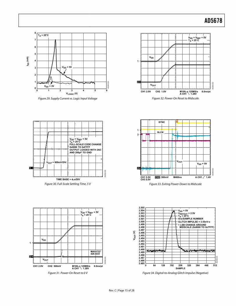
6VLOGIC (V)
I DD
(mA
)
8
0
1
5
6
7
2
3
4
0 1 2 3 4 5
0529
9-02
9
VDD = 5V
VDD = 3V
TA = 25°C
Fi e gure 29. Supply Current vs. Logic Input Voltag
0529
9-03
0
TIME BASE = 4μs/DIV
VDD = VREF = 5VTA = 25°CFULL-SCALE CODE CHANGE0x0000 TO 0xFFFFOUTPUT LOADED WITH 2kΩAND 200pF TO GND
VOUT = 909mV/DIV
1
Figure 30. Full-Scale Settling Time, 5 V
0529
9-03
1
CH1 2.0V CH2 500mV M100μs 125MS/sA CH1 1.28V
8.0ns/pt
VDD = VREF = 5VTA = 25°C
VOUT
VDD1
2
MAX(C2)*420.0mV
Figure 31. Power-On Reset to 0 V
0529
9-03
2
CH1 2.0V CH2 1.0V M100μs 125MS/sA CH1 1.28V
8.0ns/pt
VDD = VREF = 5VTA = 25°C
VOUT
VDD
1
2
Fig le ure 32. Power-On Reset to Midsca
0529
9-03
3
VDD = 5V
SYNC
SLCK
VOUT
1
3
CH1 5.0VCH3 5.0V
CH2 500mV M400ns A CH1 1.4V
2
Figure 33. Exiting Power-Down to Midscale
SAMPLE
V OU
T (V
)
2.505
2.4850 512
0529
9-03
4
64 128 192 256 320 384 448
VDD = 5VVREFOUT = 2.5VTA = 25°C4ns/SAMPLE NUMBERGLITCH IMPULSE = 3.55nV-s1 LSB CHANGE AROUND MIDSCALE (0x8000 TO 0x7FFF)
2.4862.4872.4882.4892.4902.4912.4922.4932.4942.4952.4962.4972.4982.4992.5002.5012.5022.5032.504
Figure 34. Digital-to-Analog Glitch Impulse (Negative)
AD5678
Rev. C | Page 16 of 28
SAMPLE
V OU
T (V
)
2.5000
2.49500 512
0529
9-03
52.4955
2.4960
2.4965
2.4970
2.4975
2.4980
2.4985
2.4990
2.4995
64 128 192 256 320 384 448
VDD = 5VVREFOUT = 2.5VTA = 25°C4ns/SAMPLE NUMBER
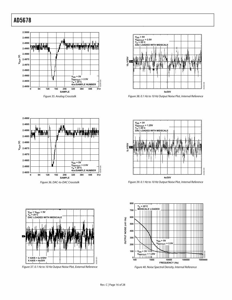
Figure 35. Analog Crosstalk
SAMPLE
V OU
T (V
)
2.4900
2.48550 512
0529
9-03
6
64 128 192 256 320 384 448
2.4860
2.4865
2.4870
2.4875
2.4880
2.4885
2.4890
2.4895
VDD = 5VVREFOTA = 2
UT = 2.5V5°C
4ns/SAMPLE NUMBER
Figure 36. DAC-to-DAC Crosstalk
0529
9-03
7
1
Y AXIS = 2μV/DIVX AXIS = 4s/DIV
VDD = VREF = 5VTA = 25°CDAC LOADED WITH MIDSCALE
Figure 37. 0.1 Hz to 10 Hz Output Noise Plot, External Reference
5s/DIV
10μV
/DIV
1
0529
9-03
8
VDD = 5VVREFOUT = 2.5VTA = 25°CDAC LOADED WITH MIDSCALE
Figure 38. 0.1 Hz to 10 Hz Output Noise Plot, Internal Reference
4s/DIV
5μV/
DIV
1
0529
9-03
9
VDD = 3VVREFOUT = 1.25VTA = 25°CDAC LOADED WITH MIDSCALE
Figure 39. 0.1 Hz to 10 Hz Output Noise Plot, Internal Reference
FREQUENCY (Hz)
OU
TPU
T N
OIS
E (n
V/√H
z)
800
0
100
9-04
0
200
300
400
500
600
700
100 100001000 100000 1000000
0529
VDD = 3VV = 1.25V
VDD = 5VVREFOUT = 2.5V
REFOUT
TA = 25°CMIDSCALE LOADED
Figure 40. Noise Spectral Density, Internal Reference
AD5678
Rev. C | Page 17 of 28
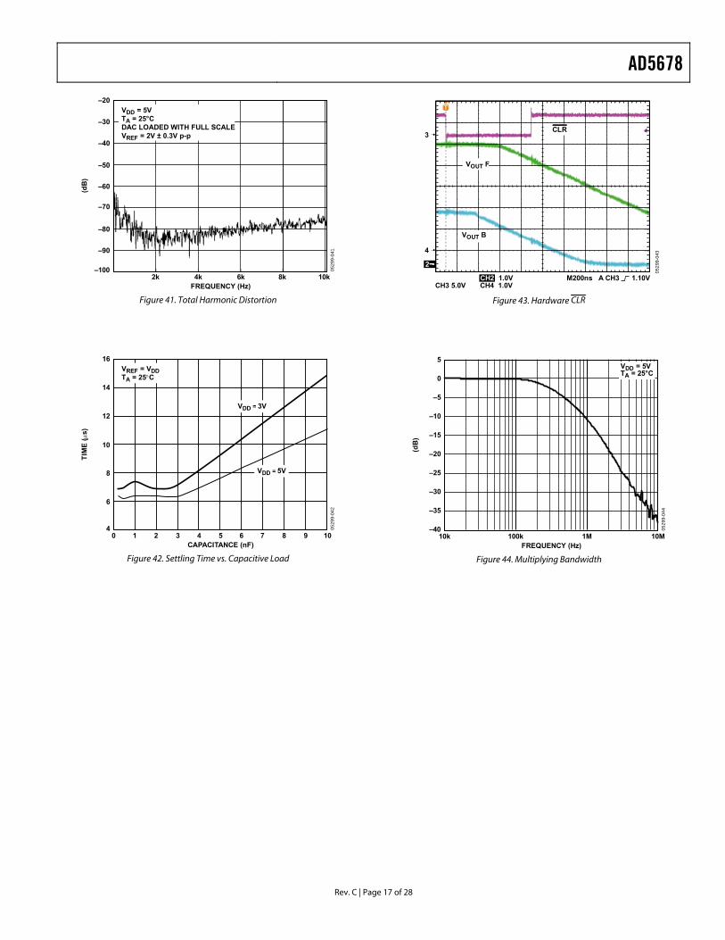
FREQUENCY (Hz)
(dB
)
–20
–50
–80
–30
–40
–60
–70
–90
–1002k 4k 6k 8k 10k
0529
9-04
1
VDD = 5VTA = 25°CDAC LOADED WITH FULL SCALEVREF = 2V ± 0.3V p-p
Figure 41. Total Harmonic Distortion
CAPACITANCE (nF)
TIM
E (μ
s)
16
14
12
10
8
6
40 1 2 3 4 5 6 7 98 1
0529
9-04
2
0
VREF = VDDTA = 25°C
VDD = 5V
VDD = 3V
Figure 42. Settling Time vs. Capacitive Load
0529
9-04
3
VOUT F
VOUT B
3
CH3 5.0V CH4 1.0VCH2 1.0V M200ns A CH3 1.10V
2
44
CLR
Figure 43. Hardware CLR
FREQUENCY (Hz)
(dB
)
5
–4010k 100k 1M 10M
0529
9-04
4–35
–30
–25
–20
–15
–10
–5
0VDD = 5VTA = 25°C
Figure 44. Multiplying Bandwidth

AD5678
Rev. C | Page 18 of 28
TERMINOLOGY Relative Accuracy For the DAC, relative accuracy, or integral nonlinearity (INL), is a measure of the maximum deviation in LSBs from a straight line passing through the endpoints of the DAC transfer function. Figure 5, Figure 7, and Figure 9 show plots of typical INL vs. code.
Differential Nonlinearity Differential nonlinearity (DNL) is the difference between the measured change and the ideal 1 LSB change between any two adjacent codes. A specified differential nonlinearity of ±1 LSB maximum ensures monotonicity. This DAC is guaranteed mono-tonic by design. Figure 6, Figure 8, and Figure 10 show plots of typical DNL vs. code.
Offset Error Offset error is a measure of the difference between the actual VOUT and the ideal VOUT, expressed in millivolts in the linear region of the transfer function. Offset error is measured on the AD5678 with Code 512 loaded into the DAC register. It can be negative or positive and is expressed in millivolts.
Zero-Code Error Zero-code error is a measure of the output error when zero code (0x0000) is loaded into the DAC register. Ideally, the output should be 0 V. The zero-code error is always positive in the AD5678, because the output of the DAC cannot go below 0 V. It is due to a combination of the offset errors in the DAC and output amplifier. Zero-code error is expressed in millivolts. Figure 18 shows a plot of typical zero-code error vs. temperature.
Gain Error
Gain error is a measure of the span error of the DAC. It is the deviation in slope of the DAC transfer characteristic from the ideal, expressed as a percentage of the full-scale range.
Zero-Code Error Drift
Zero-code error drift is a measure of the change in zero-code error with a change in temperature. It is expressed in μV/°C.
Gain Error Drift
Gain error drift is a measure of the change in gain error with changes in temperature. It is expressed in (ppm of full-scale range)/°C.
Full-Scale Error Full-scale error is a measure of the output error when full-scale code (0xFFFF) is loaded into the DAC register. Ideally, the output should be VDD − 1 LSB. Full-scale error is expressed as a percentage of the full-scale range. Figure 17 shows a plot of typical full-scale error vs. temperature.
Digital-to-Analog Glitch Impulse
Digital-to-analog glitch impulse is the impulse injected into the analog output when the input code in the DAC register changes state. It is normally specified as the area of the glitch in nV-s and is measured when the digital input code is changed by 1 LSB at the major carry transition (0x7FFF to 0x8000). See Figure 34.
DC Power Supply Rejection Ratio (PSRR) PSRR indicates how the output of the DAC is affected by changes in the supply voltage. PSRR is the ratio of the change in VOUT to a change in VDD for full-scale output of the DAC. It is measured in decibels. VREF is held at 2 V, and VDD is varied ±10%.
DC Crosstalk DC crosstalk is the dc change in the output level of one DAC in response to a change in the output of another DAC. It is measured with a full-scale output change on one DAC (or soft power-down and power-up) while monitoring another DAC. It is expressed in microvolts.
DC crosstalk due to load current change is a measure of the impact that a change in load current on one DAC has to another DAC kept at midscale. It is expressed in microvolts per milliamp.
Reference Feedthrough Reference feedthrough is the ratio of the amplitude of the signal at the DAC output to the reference input when the DAC output is not being updated (that is, LDAC is high). It is expressed in decibels.
Channel-to-Channel Isolation Channel-to-channel isolation is the ratio of the amplitude of the signal at the output of one DAC to a sine wave on the reference input of another DAC. It is measured in decibels.
Digital Feedthrough Digital feedthrough is a measure of the impulse injected into the analog output of a DAC from the digital input pins of the device, but is measured when the DAC is not being written to (SYNC held high). It is specified in nV-s and measured with a full-scale change on the digital input pins, that is, from all 0s to all 1s or vice versa.
AD5678
Rev. C | Page 19 of 28
Digital Crosstalk Digital crosstalk is the glitch impulse transferred to the output of one DAC at midscale in response to a full-scale code change (all 0s to all 1s or vice versa) in the input register of another DAC. It is measured in standalone mode and is expressed in nV-s.
Analog Crosstalk Analog crosstalk is the glitch impulse transferred to the output of one DAC due to a change in the output of another DAC. It is measured by loading one of the input registers with a full-scale code change (all 0s to all 1s or vice versa) while keeping LDAC high, and then pulsing LDAC low and monitoring the output of the DAC whose digital code has not changed. The area of the glitch is expressed in nV-s.
DAC-to-DAC Crosstalk DAC-to-DAC crosstalk is the glitch impulse transferred to the output of one DAC due to a digital code change and subsequent output change of another DAC. This includes both digital and analog crosstalk. It is measured by loading one of the DACs with a full-scale code change (all 0s to all 1s or vice versa) with LDAC low and monitoring the output of another DAC. The energy of the glitch is expressed in nV-s.
Multiplying Bandwidth The amplifiers within the DAC have a finite bandwidth. The multiplying bandwidth is a measure of this. A sine wave on the reference (with full-scale code loaded to the DAC) appears on the output. The multiplying bandwidth is the frequency at which the output amplitude falls to 3 dB below the input.
Total Harmonic Distortion (THD) Total harmonic distortion is the difference between an ideal sine wave and its attenuated version using the DAC. The sine wave is used as the reference for the DAC, and the THD is a measure of the harmonics present on the DAC output. It is measured in decibels.
AD5678
Rev. C | Page 20 of 28
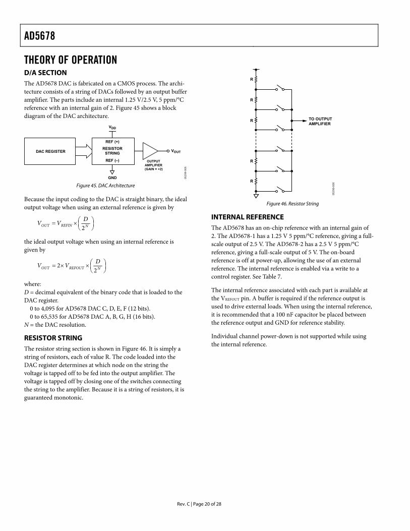
THEORY OF OPERATION D/A SECTION The AD5678 DAC is fabricated on a CMOS process. The archi-tecture consists of a string of DACs followed by an output buffer amplifier. The parts include an internal 1.25 V/2.5 V, 5 ppm/°C reference with an internal gain of 2. Figure 45 shows a block diagram of the DAC architecture.
0529
9-00
5
DAC REGISTER
REF (+)
VDD
VOUT
GND
REF (–)
RESISTORSTRING
OUTPUTAMPLIFIER(GAIN = +2)
Figure 45. DAC Architecture
Because the input coding to the DAC is straight binary, the ideal output voltage when using an external reference is given by
⎟⎠⎞
⎜⎝⎛×= NREFINOUT
DVV2
the ideal output voltage when using an internal reference is given by
⎟⎠⎞
⎜⎝⎛××= NREFOUTOUT
DVV2
2
where: D = decimal equivalent of the binary code that is loaded to the DAC register. 0 to 4,095 for AD5678 DAC C, D, E, F (12 bits). 0 to 65,535 for AD5678 DAC A, B, G, H (16 bits). N = the DAC resolution.
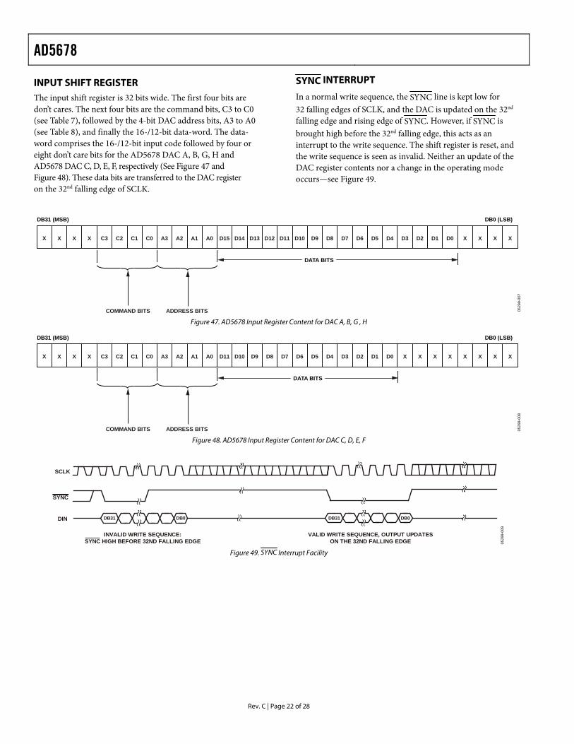
RESISTOR STRING The resistor string section is shown in Figure 46. It is simply a string of resistors, each of value R. The code loaded into the DAC register determines at which node on the string the voltage is tapped off to be fed into the output amplifier. The voltage is tapped off by closing one of the switches connecting the string to the amplifier. Because it is a string of resistors, it is guaranteed monotonic.
0529
9-00
6
TO OUTPUTAMPLIFIER
R
R
R
R
R
Figure 46. Resistor String
INTERNAL REFERENCE The AD5678 has an on-chip reference with an internal gain of 2. The AD5678-1 has a 1.25 V 5 ppm/°C reference, giving a full-scale output of 2.5 V. The AD5678-2 has a 2.5 V 5 ppm/°C reference, giving a full-scale output of 5 V. The on-board reference is off at power-up, allowing the use of an external reference. The internal reference is enabled via a write to a control register. See Table 7.
The internal reference associated with each part is available at the VREFOUT pin. A buffer is required if the reference output is used to drive external loads. When using the internal reference, it is recommended that a 100 nF capacitor be placed between the reference output and GND for reference stability.
Individual channel power-down is not supported while using the internal reference.

AD5678
Rev. C | Page 21 of 28
OUTPUT AMPLIFIER The output buffer amplifier can generate rail-to-rail voltages on its output, which gives an output range of 0 V to VDD. The amplifier is capable of driving a load of 2 kΩ in parallel with 1,000 pF to GND. The source and sink capabilities of the output amplifier can be seen in Figure 24 and Figure 25. The slew rate is 1.5 V/μs with a ¼ to ¾ scale settling time of 10 μs.
SERIAL INTERFACE The AD5678 has a 3-wire serial interface (SYNC, SCLK, and DIN) that is compatible with SPI, QSPI, and MICROWIRE interface standards as well as most DSPs. See for a timing diagram of a typical write sequence.
Figure 2
The write sequence begins by bringing the SYNC line low. Data from the DIN line is clocked into the 32-bit shift register on the falling edge of SCLK. The serial clock frequency can be as high as 50 MHz, making the AD5678 compatible with high speed DSPs. On the 32nd falling clock edge, the last data bit is clocked in and the programmed function is executed, that is, a change in DAC register contents and/or a change in the mode of operation. At this stage, the SYNC line can be kept low or be brought high. In either case, it must be brought high for a minimum of 15 ns before the next write sequence so that a falling edge of SYNC can initiate the next write sequence. Because the SYNC buffer draws more current when VIN = 2 V than it does when VIN = 0.8 V, SYNC should be idled low between write sequences for even lower power operation of the part. As is mentioned previously, however, SYNC must be brought high again just before the next write sequence.
Table 7. Command Definitions Command
C3 C2 C1 C0 Description 0 0 0 0 Write to Input Register n 0 0 0 1 Update DAC Register n 0 0 1 0 Write to Input Register n, update all
(software LDAC)
0 0 1 1 Write to and update DAC Channel n 0 1 0 0 Power down/power up DAC 0 1 0 1 Load clear code register 0 1 1 0 Load LDAC register
0 1 1 1 Reset (power-on reset) 1 0 0 0 Set up internal REF register 1 0 0 1 Reserved – – – – Reserved 1 1 1 1 Reserved
Table 8. Address Commands Address (n)
A3 A2 A1 A0 Selected DAC Channel
0 0 0 0 DAC A (16 bits) 0 0 0 1 DAC B (16 bits) 0 0 1 0 DAC C (12 bits) 0 0 1 1 DAC D (12 bits) 0 1 0 0 DAC E (12 bits) 0 1 0 1 DAC F (12 bits) 0 1 1 0 DAC G (16 bits) 0 1 1 1 DAC H (16 bits) 1 1 1 1 All DACs
AD5678
Rev. C | Page 22 of 28
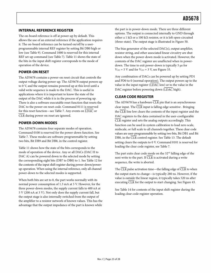
INPUT SHIFT REGISTER The input shift register is 32 bits wide. The first four bits are don’t cares. The next four bits are the command bits, C3 to C0 (see Table 7), followed by the 4-bit DAC address bits, A3 to A0 (see Table 8), and finally the 16-/12-bit data-word. The data-word comprises the 16-/12-bit input code followed by four or eight don’t care bits for the AD5678 DAC A, B, G, H and AD5678 DAC C, D, E, F, respectively (See Figure 47 and Figure 48). These data bits are transferred to the DAC register on the 32nd falling edge of SCLK.
SYNC INTERRUPT
In a normal write sequence, the SYNC line is kept low for 32 falling edges of SCLK, and the DAC is updated on the 32nd falling edge and rising edge of SYNC. However, if SYNC is brought high before the 32nd falling edge, this acts as an interrupt to the write sequence. The shift register is reset, and the write sequence is seen as invalid. Neither an update of the DAC register contents nor a change in the operating mode occurs—see Figure 49.
0529
9-00
7
ADDRESS BITSCOMMAND BITS
C3 C2 C1 C0 A3 A2 A1 A0 D15 D14 D13 D12 D11 D10 D9 D8 D7 D6 D5 D4 D3 D2 D1 D0 X X X XX X X X
DB31 (MSB) DB0 (LSB)
DATA BITS
Figure 47. AD5678 Input Register Content for DAC A, B, G , H
0529
9-00
8
ADDRESS BITSCOMMAND BITS
C3 C2 C1 C0 A3 A2 A1 A0 D11 D10 D9 D8 D7 D6 D5 D4 D3 D2 D1 D0 X X X X X X X XX X X X
DB31 (MSB) DB0 (LSB)
DATA BITS
Figure 48. AD5678 Input Register Content for DAC C, D, E, F
0529
9-00
9
SCLK
DIN DB31 DB0
INVALID WRITE SEQUENCE:SYNC HIGH BEFORE 32ND FALLING EDGE
VALID WRITE SEQUENCE, OUTPUT UPDATESON THE 32ND FALLING EDGE
DB31 DB0
SYNC
Figure 49. SYNC Interrupt Facility
AD5678
Rev. C | Page 23 of 28
INTERNAL REFERENCE REGISTER The on-board reference is off at power-up by default. This allows the use of an external reference if the application requires it. The on-board reference can be turned on/off by a user-programmable internal REF register by setting Bit DB0 high or low (see Table 9). Command 1000 is reserved for this internal REF set-up command (see Table 7). Table 11 shows the state of the bits in the input shift register corresponds to the mode of operation of the device.
POWER-ON RESET The AD5678 contains a power-on reset circuit that controls the output voltage during power-up. The AD5678 output powers up to 0 V, and the output remains powered up at this level until a valid write sequence is made to the DAC. This is useful in applications where it is important to know the state of the output of the DAC while it is in the process of powering up. There is also a software executable reset function that resets the DAC to the power-on reset code. Command 0111 is reserved for this reset function—see Table 7. Any events on LDAC or CLR during power-on reset are ignored.
POWER-DOWN MODES The AD5678 contains four separate modes of operation. Command 0100 is reserved for the power-down function. See Table 7. These modes are software-programmable by setting two bits, Bit DB9 and Bit DB8, in the control register.
Table 11 shows how the state of the bits corresponds to the mode of operation of the device. Any or all DACs (DAC H to DAC A) can be powered down to the selected mode by setting the corresponding eight bits (DB7 to DB0) to 1. See Table 12 for the contents of the input shift register during power-down/power-up operation. When using the internal reference, only all channel power-down to the selected modes is supported.
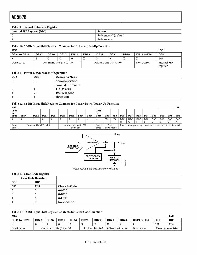
When both bits are set to 0, the part works normally with its normal power consumption of 1.3 mA at 5 V. However, for the three power-down modes, the supply current falls to 400 nA at 5 V (200 nA at 3 V). Not only does the supply current fall, but the output stage is also internally switched from the output of the amplifier to a resistor network of known values. This has the advantage that the output impedance of the part is known while
the part is in power-down mode. There are three different options. The output is connected internally to GND through either a 1 kΩ or a 100 kΩ resistor, or it is left open-circuited (three-state). The output stage is illustrated in Figure 50.
The bias generator of the selected DAC(s), output amplifier, resistor string, and other associated linear circuitry are shut down when the power-down mode is activated. However, the contents of the DAC register are unaffected when in power-down. The time to exit power-down is typically 5 μs for VDD = 5 V and for VDD = 3 V, see Figure 33.
Any combination of DACs can be powered up by setting PD1 and PD0 to 0 (normal operation). The output powers up to the value in the input register (LDAC low) or to the value in the DAC register before powering down (LDAC high).
CLEAR CODE REGISTER The AD5678 has a hardware CLR pin that is an asynchronous clear input. The CLR input is falling edge sensitive . Bringing the CLR line low clears the contents of the input register and the DAC registers to the data contained in the user-configurable CLR register and sets the analog outputs accordingly. This function can be used in system calibration to load zero scale, midscale, or full scale to all channels together. These clear code values are user-programmable by setting two bits, Bit DB1 and Bit DB0, in the CLR control register. See . The default setting clears the outputs to 0 V. Command 0101 is reserved for loading the clear code register, see .
Table 13
Table 7
The part exits clear code mode on the 32nd falling edge of the next write to the part. If CLR is activated during a write sequence, the write is aborted.
The CLR pulse activation time—the falling edge of CLR to when the output starts to change—is typically 280 ns. However, if the value is outside the linear region, it typically takes 520 ns after executing CLR for the output to start changing. See . Figure 43
See Table 14 for contents of the input shift register during the loading clear code register operation.
AD5678
Rev. C | Page 24 of 28
Table 9. Internal Reference Register Internal REF Register (DB0) Action 0 Reference off (default) 1 Reference on
Table 10. 32-Bit Input Shift Register Contents for Reference Set-Up Function MSB LSB
DB31 to DB28 DB27 DB26 DB25 DB24 DB23 DB22 DB21 DB20 DB19 to DB1 DB0 X 1 0 0 0 X X X X X 1/0 Don’t cares Command bits (C3 to C0) Address bits (A3 to A0) Don’t cares Internal REF
register
Table 11. Power-Down Modes of Operation DB9 DB8 Operating Mode 0 0 Normal operation Power-down modes 0 1 1 kΩ to GND 1 0 100 kΩ to GND 1 1 Three-state
Table 12. 32-Bit Input Shift Register Contents for Power-Down/Power-Up Function MSB LSB
DB31 to DB28 DB27 DB26 DB25 DB24 DB23 DB22 DB21 DB20
DB19 to DB10 DB9 DB8 DB7 DB6 DB5 DB4 DB3 DB2 DB1 DB0
X 0 1 0 0 X X X X X PD1 PD0 DAC H
DAC G
DAC F
DAC E
DAC D
DAC C
DAC B
DAC A
Don’t cares
Command bits (C3 to C0) Address bits (A3 to A0)— don’t cares
Don’t cares
Power-down mode
Power-down/power-up channel selection—set bit to 1 to select
RESISTORNETWORK
VOUT
VFB
RESISTORSTRING DAC
0529
9-01
0
POWER-DOWNCIRCUITRY
AMPLIFIER
Figure 50. Output Stage During Power-Down
Table 13. Clear Code Register Clear Code Register
DB1 DB0 CR1 CR0 Clears to Code 0 0 0x0000 0 1 0x8000 1 0 0xFFFF 1 1 No operation
Table 14. 32-Bit Input Shift Register Contents for Clear Code Function MSB LSB
DB31 to DB28 DB27 DB26 DB25 DB24 DB23 DB22 DB21 DB20 DB19 to DB2 DB1 DB0 X 0 1 0 1 X X X X X CR1 CR0 Don’t cares Command bits (C3 to C0) Address bits (A3 to A0)—don’t cares Don’t cares Clear code register
AD5678
Rev. C | Page 25 of 28
LDAC FUNCTION
The outputs of all DACs can be updated simultaneously using the hardware LDAC pin.
Synchronous LDAC: After new data is read, the DAC registers are updated on the falling edge of the 32nd SCLK pulse. LDAC can be permanently low or pulsed as in . Figure 2
Asynchronous LDAC: The outputs are not updated at the same time that the input registers are written to. When LDAC goes low, the DAC registers are updated with the contents of the input register.
Alternatively, the outputs of all DACs can be updated simulta-neously using the software LDAC function by writing to Input Register n and updating all DAC registers. Command 0011 is reserved for this software LDAC function.
An LDAC register gives the user extra flexibility and control over the hardware LDAC pin. This register allows the user to select which combination of channels to simultaneously update when the hardware LDAC pin is executed. Setting the LDAC bit register to 0 for a DAC channel means that this channel’s update is controlled by the LDAC pin. If this bit is set to 1, this channel updates synchronously; that is, the DAC register is updated after new data is read, regardless of the state of the LDAC pin. It effectively sees the LDAC pin as being tied low. (See for the
Table 15LDAC register mode of operation.) This flexibility is
useful in applications where the user wants to simultaneously update select channels while the rest of the channels are synchronously updating.
Writing to the DAC using command 0110 loads the 8-bit LDAC register (DB7 to DB0). The default for each channel is 0; that is, the LDAC pin works normally. Setting the bits to 1 means the DAC channel is updated regardless of the state of the LDAC pin. See for the contents of the input shift register during the load
Table 16LDAC register mode of operation.
POWER SUPPLY BYPASSING AND GROUNDING When accuracy is important in a circuit, it is helpful to carefully consider the power supply and ground return layout on the board. The printed circuit board containing the AD5678 should have separate analog and digital sections. If the AD5678 is in a system where other devices require an AGND-to-DGND connection, the connection should be made at one point only. This ground point should be as close as possible to the AD5678.
The power supply to the AD5678 should be bypassed with 10 μF and 0.1 μF capacitors. The capacitors should physically be as close as possible to the device, with the 0.1 μF capacitor ideally right up against the device. The 10 μF capacitors are the tantalum bead type. It is important that the 0.1 μF capacitor has low effective series resistance (ESR) and low effective series inductance (ESI), such as is typical of common ceramic types of capacitors. This 0.1 μF capacitor provides a low impedance path to ground for high frequencies caused by transient currents due to internal logic switching.
The power supply line should have as large a trace as possible to provide a low impedance path and reduce glitch effects on the supply line. Clocks and other fast switching digital signals should be shielded from other parts of the board by digital ground. Avoid crossover of digital and analog signals if possible. When traces cross on opposite sides of the board, ensure that they run at right angles to each other to reduce feedthrough effects through the board. The best board layout technique is the microstrip technique, where the component side of the board is dedicated to the ground plane only and the signal traces are placed on the solder side. However, this is not always possible with a 2-layer board.
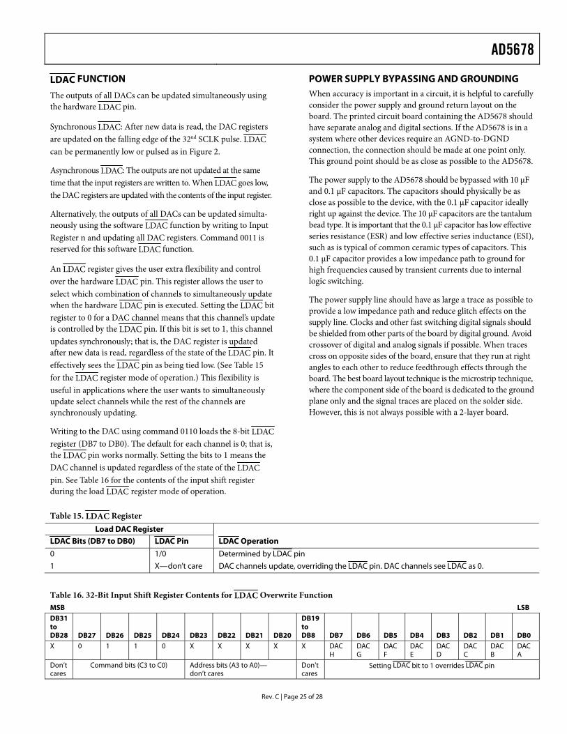
Table 15. LDAC Register
Load DAC Register
LDAC Bits (DB7 to DB0) LDAC Pin LDAC Operation
0 1/0 Determined by LDAC pin
1 X—don’t care DAC channels update, overriding the LDAC pin. DAC channels see LDAC as 0.
Table 16. 32-Bit Input Shift Register Contents for LDAC Overwrite Function MSB LSB
DB31 to DB28 DB27 DB26 DB25 DB24 DB23 DB22 DB21 DB20
DB19to DB8 DB7 DB6 DB5 DB4 DB3 DB2 DB1 DB0
X 0 1 1 0 X X X X X DAC H
DAC G
DAC F
DAC E
DAC D
DAC C
DAC B
DAC A
Don’t cares
Command bits (C3 to C0) Address bits (A3 to A0)— don’t cares
Don’tcares
Setting LDAC bit to 1 overrides LDAC pin
AD5678
Rev. C | Page 26 of 28
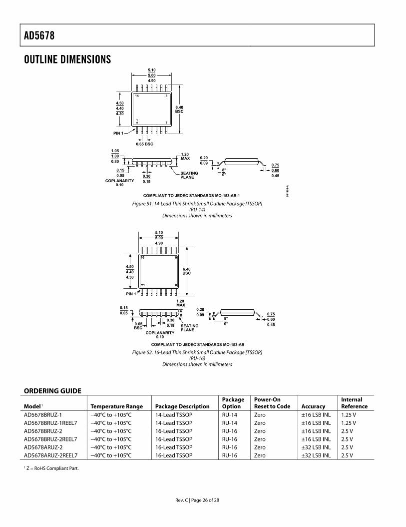
OUTLINE DIMENSIONS
COMPLIANT TO JEDEC STANDARDS MO-153-AB-1 0619
08-A
8°0°
4.504.404.30
14 8
71
6.40BSC
PIN 1
5.105.004.90
0.65 BSC
0.150.05 0.30
0.19
1.20MAX
1.051.000.80
0.200.09 0.75
0.600.45
COPLANARITY0.10
SEATINGPLANE
Figure 51. 14-Lead Thin Shrink Small Outline Package [TSSOP]
(RU-14) Dimensions shown in millimeters
16 9
81
PIN 1
SEATINGPLANE
8°0°
4.504.404.30
6.40BSC
5.105.004.90
0.65BSC
0.150.05
1.20MAX
0.200.09 0.75
0.600.45
0.300.19
COPLANARITY0.10
COMPLIANT TO JEDEC STANDARDS MO-153-AB Figure 52. 16-Lead Thin Shrink Small Outline Package [TSSOP]
(RU-16) Dimensions shown in millimeters
ORDERING GUIDE
Model1 Temperature Range Package Description Package Option
Power-On Reset to Code Accuracy
Internal Reference
AD5678BRUZ-1 −40°C to +105°C 14-Lead TSSOP RU-14 Zero ±16 LSB INL 1.25 V AD5678BRUZ-1REEL7 −40°C to +105°C 14-Lead TSSOP RU-14 Zero ±16 LSB INL 1.25 V AD5678BRUZ-2 −40°C to +105°C 16-Lead TSSOP RU-16 Zero ±16 LSB INL 2.5 V AD5678BRUZ-2REEL7 −40°C to +105°C 16-Lead TSSOP RU-16 Zero ±16 LSB INL 2.5 V AD5678ARUZ-2 −40°C to +105°C 16-Lead TSSOP RU-16 Zero ±32 LSB INL 2.5 V AD5678ARUZ-2REEL7 −40°C to +105°C 16-Lead TSSOP RU-16 Zero ±32 LSB INL 2.5 V 1 Z = RoHS Compliant Part.

AD5678
Rev. C | Page 27 of 28
NOTES

AD5678
Rev. C | Page 28 of 28
NOTES
©2005–2011 Analog Devices, Inc. All rights reserved. Trademarks and registered trademarks are the property of their respective owners. D05299–0–2/11(C)