2.5/3d ics systems · eda 2 asic 2.5/3d ics technical and business considerations herb reiter,...
TRANSCRIPT

eda 2 asic
2.5/3D ICs
Technical AND Business Considerations
Herb Reiter, eda2asic Consulting, Inc. [email protected], 1-408-981-5831
MEPTEC Luncheon, June 13, 2012
Systems

eda 2 asic AGENDA
• Introduction
• A few market numbers
• Why develop 2.5/3D solutions ?
• What’s different in the 2.5/3D ecosystem ?
• 2.5/3D products TODAY
• Opportunities for MEPTEC members
• Appendix: Additional market data

eda 2 asic Herb Reiter’s Background
2000
1990
1980
Magister (= MBA) & MSEE in Austria
‘80: National Semi Europe , PLD Mktg
‘83: National Semi U.S., ASIC Mktg
’89: VLSI Technology Alliances, ASICs & ASSPs Mktg
‘97: ViewLogic, ASIC Alliances ‘98: Synopsys, Semicond. Alliances
‘00: Barcelona Design, Alliances
’02: eda2asic Consulting, Inc.
Biz Dev for New Technologies
’86: MBA, San Jose State
Synplicity, Structured ASIC Tools
ReShape, IC Design Flow
Gradient, Temp Analysis, ICs
Flomerics, Temp Analysis, PCB
AMD, Opteron Mktg to EDA
GDA, Design Services Biz Plan
Takumi, DFM Tools & Services
Innovative Silicon, ZRAM-IP
S3 Group, Analog & M/S IP
Philips, Clockless IC Design
Mentor, C RTL Synthesis
Mephisto DA, Analog Sizing
Ciranova, Analog Layout
GeorgiaTech, SiP Noise Analysis
Soitec & SOI Consortium, SOI
GSA, 3D-IC Working Group
SEMATECH, 3D Enablement Ctr
Stanford: Continuing Education
2010 10 years of bridging the gap between EDA tools and ASIC design challenges

eda 2 asic
Market Numbers
eda 2 asic 2016 Market Size Forecast
Auto
Computer
Consumer Comms
Industrial
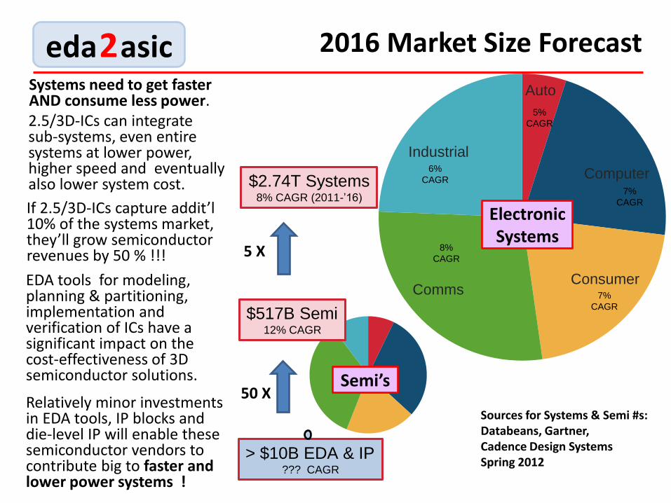
$2.74T Systems 8% CAGR (2011-’16)
5%
CAGR
7%
CAGR
7%
CAGR
6%
CAGR
8%
CAGR
$517B Semi 12% CAGR
> $10B EDA & IP ??? CAGR
Sources for Systems & Semi #s: Databeans, Gartner, Cadence Design Systems Spring 2012
5 X
50 X
EDA tools for modeling, planning & partitioning, implementation and verification of ICs have a significant impact on the cost-effectiveness of 3D semiconductor solutions.
Electronic Systems
Semi’s
2.5/3D-ICs can integrate sub-systems, even entire systems at lower power, higher speed and eventually also lower system cost.
If 2.5/3D-ICs capture addit’l 10% of the systems market, they’ll grow semiconductor revenues by 50 % !!!
Relatively minor investments in EDA tools, IP blocks and die-level IP will enable these semiconductor vendors to contribute big to faster and lower power systems !
Systems need to get faster AND consume less power.
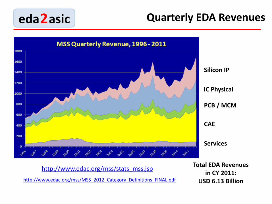
eda 2 asic Quarterly EDA Revenues
Silicon IP
IC Physical
PCB / MCM
CAE
Services
http://www.edac.org/mss/stats_mss.jsp
http://www.edac.org/mss/MSS_2012_Category_Definitions_FINAL.pdf
Total EDA Revenues in CY 2011:
USD 6.13 Billion

eda 2 asic ~30% of Semiconductor Revenue is…
http://www.semi.org/en/node/41166
eda 2 asic
Why Develop 2.5/3D Solutions ?

eda 2 asic Key Motivators
Reduce system cost
Reduce power dissipation
Reduce form factor
Increase system complexity/user friendliness
Increase performance per Watt
Increase reliability
Decrease time-to-market
Decrease NRE and risk

eda 2 asic Challenges for Feature Size Shrinking
Source: International Business Strategies 2010
Wafer Fab cost
Cost per gate
Variability
Risk, TTM
Design Cost
Mask Cost
Yield Variations

eda 2 asic Energy per Operation (64 bit words)
DDR3 4.8 nJ/word
MIPS 64 core 400 pJ/cycle
45 nm 0.8 V FPU 38 pJ/Op
20 mV I/O 128 pJ/Word
LPDDR2 512 pJ/Word
SERDES I/O 1.9 nJ/Word
On-chip/mm 7 pJ/Word
TSV I/O (ESD) 7 pJ/Word
TSV I/O (secondary ESD) 2 pJ/Word
Optimized DRAM core 128 pJ/word
11 nm 0.4 V core 200 pJ/op
1 cm / high-loss interposer 300 pJ/Word
Dr. Paul Franzon, NCSU, June 2012
0.4 V / low-loss interposer 45 pJ/Word

eda 2 asic Cost Comparison for Mixed-Signal ICs
Heterogeneous integration on one die is usually expensive
3D stacking reduces cost for heterogeneous integration
Courtesy: Borkar, Intel Yuan Xie, Penn State Univ.

eda 2 asic TSV Enabled Benefits
Design Automation Conference, San Francisco, June 2012

eda 2 asic
What’s Different in the 2.5/3D Eco-System?

eda 2 asic Application Specific Requirements
http://www.lbl.gov/Science-Articles/Archive/data-center-energy-myth.html
http://www.ilshayeb.com/?p=1494
Mobile Devices Data Centers
Battery Life in minutes
Battery Life and System Price !!! Operating & Cooling Cost !!!

eda 2 asic
SYSTEM-level H/W + S/W planning & partitioning,…
Changes Needed for 2.5/3D-ICs
Materials for die, interposer, substrate, package,…
Test and Assembly KGD, (partial) stack testing,…
Thin Wafer Handling bond-, debond, ship,..
Wafer Manufacturing TSV etch, -fill, w-probe,…
thinning, RDL,…
Business Model profit & responsibilities sharing
Die-InterPoser-Pkg-Board co-design, die-level IP, DFT,...
Single Die, Stack, In-System verification, debug,…
Systems
Pathfinding

eda 2 asic EDA Vendors Driving Standards
Designers
Manufacturers Fab, Assembly, Test
Design
Rules,
Libraries,
Models Design
Files and
Test
Programs
Design tools
Modeling tools
Standards for
Hand-off Criteria
Libraries, IP, Dice,…
Standards .
EDA Vendors
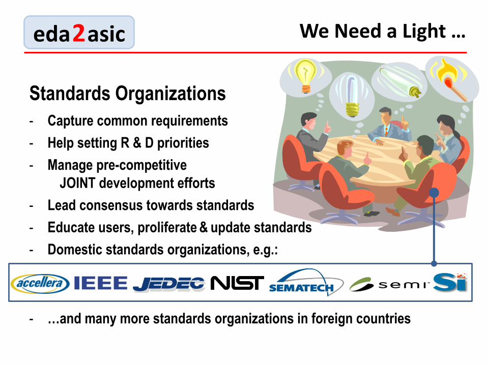
eda 2 asic We Need a Light …
Standards Organizations
- Capture common requirements
- Help setting R & D priorities
- Manage pre-competitive
JOINT development efforts
- Lead consensus towards standards
- Educate users, proliferate & update standards
- Domestic standards organizations, e.g.:
- …and many more standards organizations in foreign countries

eda 2 asic
MISSION: Accelerating the next technology revolution
Research Development Manufacturing
3D Enablement Center Members: ADI, Altera, ASE, Invensas, LSI, NIST, ON Semi, Qualcomm
3D Interconnect Program Member: Hynix
SEMATECH Core Members: CNSE, Global Foundries, IBM, Intel, Samsung, TSMC SEMATECH Standards Dashboard at: http://wiki.sematech.org/3D-Standards

eda 2 asic Closed vs Open Innovation Principles
http://www.inventorium.org/2012/04/10/open-innovation/oi/
We don’t have to originate the research to profit from it.
External R&D can create significant value; internal R&D is needed to claim some portion of that value.
Not all smart people in the field work for us. We need to work with smart people inside AND outside our company.
Building a better business model is better than getting to the market first.
If we make the best use of internal and external ideas, we will win.
We should profit from others’ use of our IP, and we should buy others’ IP whenever it advances our business model.
If we discover it ourselves, we will get it to market first.
To profit from R&D we must discover it, develop it and ship it ourselves
The smart people in the field work for us.
The company that gets an innovation to the market first, will win.
If we create the most and best ideas in industry, we will win.
We should control our IP so that our competitors don’t profit from our ideas.
CLOSED OPEN
1
2
3
4
5
6

eda 2 asic In the Good Old Times …
Development- and
Per-Unit Cost
Production Volume
FPGA Gate Array
Cell-based/COT
Use FPGA Use Gate Array Use Cell-based/COT
Total COST and Time-to-Market were the dominant criteria for technology selection
Time to Market: 1 Week to Months Months to Quarters Quarters to Years
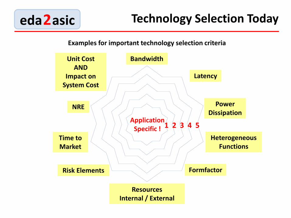
eda 2 asic Technology Selection Today
Examples for important technology selection criteria
Bandwidth
Latency
Power Dissipation
Formfactor
Resources Internal / External
NRE
Risk Elements
Time to Market
Heterogeneous Functions
Unit Cost AND
Impact on System Cost
1 2 3 4 5 Application
Specific !

eda 2 asic Tomorrow: 2.5/3D System Integration
Source: Rao Tummala, Georgia Institute of Technology, 3D Systems Packaging Research Center, Oct 2010
eda 2 asic
2.5 / 3D Products TODAY

eda 2 asic Technology Comparisons
http://www.design-reuse.com/articles/exit/?id=14887&url=http%3A%2F%2Fwww.commsdesign.com%2Farticle%2FprintableArticle.jhtml%3FarticleID%3D196700054
PoP SiP Interposer 3D/TSV
Package Thickness
Power Dissipation
Access Time
Bandwidth
Industry Readiness
limited o.k. good best
Memory Logic
SoC and SiP, combined in a PoP
PoP cross-section from www.ifixit.com
eda 2 asic

eda 2 asic Copper Pillars vs Solder Bumps
http://www.edn.com/article/print/521939-Die_to_die_bonding_using_copper_pillars.php

eda 2 asic Wide I/O Standard
Standardized by JEDEC 42.6
Published in December 2011 Twice the bandwidth of LPDDR2 at the same power Mobile HD video: 12.8 MB/sec 4 channels, each 128 data bits 1200 total connections
1.2V CMOS signal levels Pad-pitch 40 x 50 microns
Boundary scan to test I/C
Locations of thermal sensors
Exact mechanical dimensions (defined by JC 11)
Courtesy: Intel and JC 42.6

eda 2 asic Wide I/O Standard
JEDEC (JC 42.6) released Q4, 2011 the first Wide I/O Standard
TWICE the Bandwidth at the same Power Dissipation as LPDDR2
Drivers: Samsung, Elpida, Hynix, Micron, Qualcomm, TI, Intel, AMD, ST, Apple, Advantest and others
Sophie Dumas, STEricsson
Wioming Test-Chip
http://eda360insider.wordpress.com/2011/12/14/3d-week-wide-io-sdram-network-on-chip-multicore-tsv-asynchronous-logic-3d-soc-stack-from-cea-leti-and-st-ericsson-hits-all-the-advanced-notes-can-you-say-tour-de-force/

eda 2 asic Hybrid Memory Cube
HMC Consortium founded by Micron and Samsung in Oct 2011.
HMC combines high-speed logic process technology with a stack of through-silicon-via (TSV) bonded memory die.
A single HMC can provide more than 15x the performance of a DDR3 module.
Utilizes 70% less energy per bit than DDR3 DRAM technologies..
HMC increases density per bit and reduces form factor - nearly 90% less space than today's RDIMMs.
http://hybridmemorycube.org/technology.html

eda 2 asic Quad FPGA in a Package
Courtesy: Xilinx Power of these 4 FPGAs: 18 Watts Versus 120 Watts if individually packaged
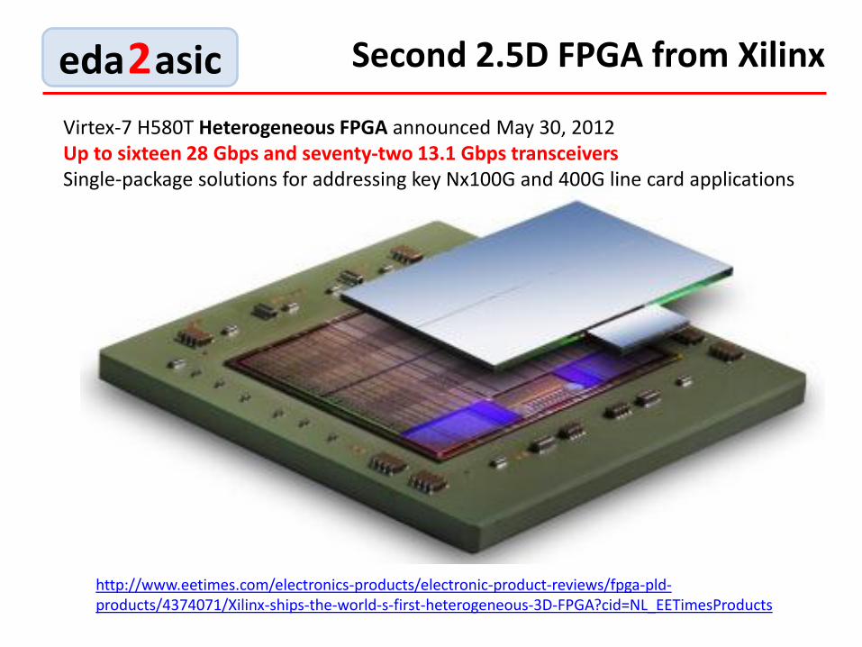
eda 2 asic Second 2.5D FPGA from Xilinx
http://www.eetimes.com/electronics-products/electronic-product-reviews/fpga-pld-products/4374071/Xilinx-ships-the-world-s-first-heterogeneous-3D-FPGA?cid=NL_EETimesProducts
Virtex-7 H580T Heterogeneous FPGA announced May 30, 2012 Up to sixteen 28 Gbps and seventy-two 13.1 Gbps transceivers Single-package solutions for addressing key Nx100G and 400G line card applications

eda 2 asic Altera/TSMC Testchip
http://www.electroiq.com/blogs/insights_from_leading_edge/2012.html
EDA Readiness / Challenges TSMC’s 2.5D Technology: CoWoS = Chip on Wafer on Substrate
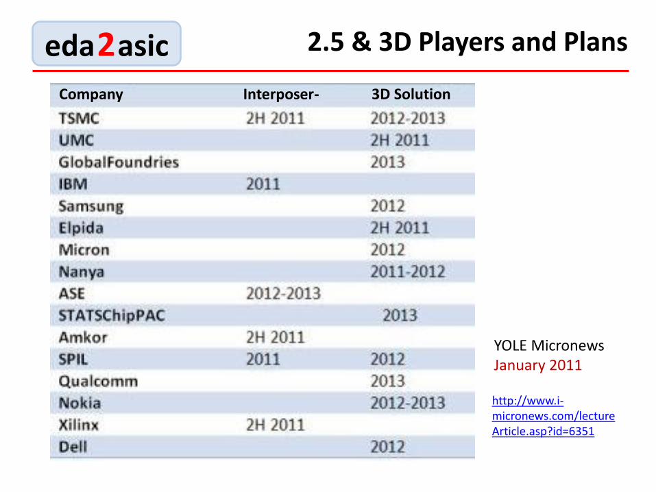
eda 2 asic 2.5 & 3D Players and Plans
http://www.i-micronews.com/lectureArticle.asp?id=6351
YOLE Micronews January 2011
Company Interposer- 3D Solution
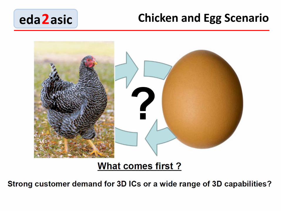
eda 2 asic Chicken and Egg Scenario
eda 2 asic
Opportunities for MEPTEC Members MicroElectronics, Packaging and Test Engineering Council

eda 2 asic Cost-Effective Billion-Transistor Chips
Source: Yuan Xie, PSU

eda 2 asic Growth Drivers Through 2014
CAGR 2009 – 14 in %
2014 Semiconductor revenues in B$
Mobile PCs
Smartphone LCD TV
Small Servers
Fiber Broadband
Laser DVD
IP STB
SSD
Media Tablet
Red = Consumer Products
Space- and Power constraint

eda 2 asic 2.5/3D-ICs: Protos to Production
System- & IC-level Planning
System- & ICs Implementation
In-System- & ICs Verification Design
Hand-off to Manu- facturing
(Die-level) IP blocks
Wafer Manuf.
EDA Tools & Flows
PDK: Design Rules & Libraries
Wafer Probe
Thinning, TSV Reveal RDL
Die Stacking, Assy & Test
Final 3D-IC Test & QA
Wafer Fab Equipment
Assembly Equipment Test Equipment
OS and Appl. Software
Design Manufacturing
Design & Engineering Services
Protos for Eval,
then Production
Equipment and Wafer-, Package-, Materials Suppliers
Modeling Information
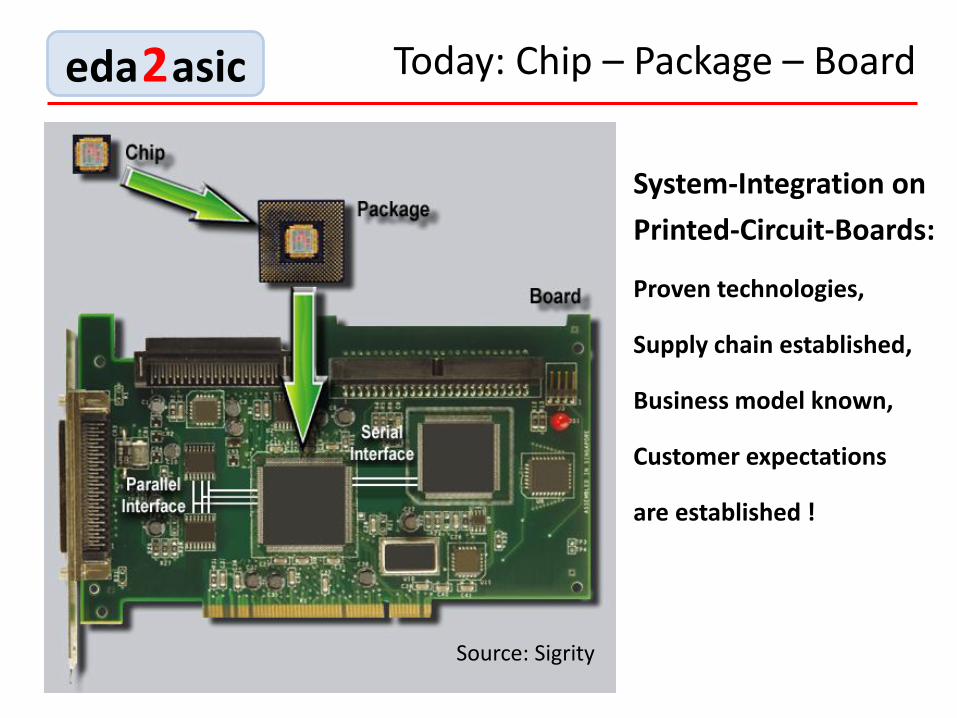
eda 2 asic Today: Chip – Package – Board
Source: Sigrity
System-Integration on
Printed-Circuit-Boards:
Proven technologies,
Supply chain established,
Business model known,
Customer expectations
are established !

eda 2 asic Systems: Protos to Production
System- level Planning
System Implementation
System Verification
Software 2.5/3D Hardware Components
(Sub)system Assembly
PCB Test PCB Assembly
Protos building & bench testing
(Sub)system Design Hand-off to Manufacturing
Software 2.5/3D Hardware Components
Buffer Inventory
(Sub)system Test
Shipping
Buffer Inventory

eda 2 asic 3D Integration – Impact on System
IMAPS Int. Conf. Device, Packaging, Scottsdale, March 10, 2011
Electrical
Thermal Mechanical
Performance and
Reliability
Electromigration Electro-thermal
interactions
Thermo-mechanical
stress
Ref.: A. Wilde, P. Schneider, P. Ramm, DTC 2010
New Materials and Manufacturing Flows
to mitigate these

eda 2 asic 3D/TSV Manufacturing Challenges
Wafer manufacturing • TSV Etching • TSV Insulating • TSV Filling (Cu or ..) • Thermal/mechanical stress • Via first/middle/last • Wafer probing • Size: 5 x 50 2 x 40 um
Wafer thinning • Bonding • Thinning, reveal • RDL • De-bonding • Shipping/Handling
Stacking/Packaging/Test • D2D / D2W / W2W • Alignment Accuracy • Micro-bumping • Cu-Cu direct bonding • Packaging • Partial/final stack test

eda 2 asic 2.5/3D Testing
http://www.gsaglobal.org/forum/2012/1/articles_ge_capital_global.asp
P 1838 Working Group proposed 3D DFT strategy
ITRS works on test roadmap
Industry organizations driving further considerations:
- Known-good-die
- Probe cards ( 40x50u )
- Passive interposer test
- Stack accessibility
- Mixed-signal test
- Stack-in-progress test
- Test program(s) generation
- Stack overheating @ test
- Yield / Redundancy
- Who tests ( Fab / OSAT )
- Who pays for yield-loss…

eda 2 asic
Appendix: Market Data

eda 2 asic Top 10 Semiconductor Buyers
http://www.zdnet.com/blog/btl/gartner-apple-jumped-to-top-semiconductor-company-in-2011/67849

eda 2 asic Top 25 Semiconductor Vendors in 2011

eda 2 asic 2012 Revenue Shares
http://www.ems007.com/pages/zone.cgi?artcatid=0&a=81742&artid=81742&pg=2
Databeans Estimates, Febr 2012
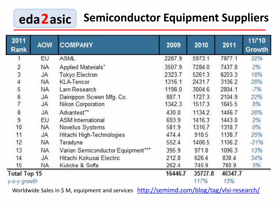
eda 2 asic Semiconductor Equipment Suppliers
http://semimd.com/blog/tag/vlsi-research/ Worldwide Sales in $ M, equipment and services

eda 2 asic Semiconductor Capex
http://semimd.com/blog/tag/vlsi-research/

eda 2 asic Major Foundries
IC Insights 2011, referenced in ( ESNUG 503 Item 6 ) by John Cooley [05/04/12]

eda 2 asic
http://www.businessinsider.com/apple-earnings-june-quarter-2011-7#ixzz1TEhyOPbg
Apple Delivers A Massive Blow Out Thanks To Huge iPhone And iPad Sales Jay Yarow | Jul. 19, 2011
Apple's earnings are out and it's another monster quarter for the company as iPhone and iPad sales blew away estimates. It earned $7.31 billion in net profit on revenue of $28.57 billion for the June quarter. Both are records for Apple. iPad shipments: 9.25 M#/Q
Wedbush Securities are estimating that some one million iPad 2s sold over the first weekend

eda 2 asic
http://arstechnica.com/civis/viewtopic.php?p=22817348

eda 2 asic Real Leadership Lessons of Steve Jobs
Focus Simplify Take responsibility end to end When behind, leapfrog Put products before profits Don’t be a slave to focus groups Bend reality Impute Push for perfection Tolerate only “A” players Engage face-to-face Know both the big picture and the details Combine the humanities with the sciences Stay hungry, stay foolish
http://hbr.org/2012/04/the-real-leadership-lessons-of-steve-jobs/ar/1

eda 2 asic