2300 ieee journal of solid-state circuits, vol. 46, no. 10
TRANSCRIPT

2300 IEEE JOURNAL OF SOLID-STATE CIRCUITS, VOL. 46, NO. 10, OCTOBER 2011
A Fast Phase Tracking ADPLL for Video Pixel ClockGeneration in 65 nm CMOS Technology
Ching-Che Chung, Member, IEEE, and Chiun-Yao Ko
Abstract—A phase-locked loop (PLL) for analog video RGBsignal acquisition interface requires precise clock generation froma very noisy and low-frequency horizontal synchronization signal(HSYNC). In such applications, the frequency multiplication ratiois always larger than 800 and can be up to over 2600. The outputpixel clock has to be phase aligned to the HSYNC. Otherwise,the displayed image will become blurry. A fast phase trackingall-digital PLL (ADPLL) for video pixel clock generation in a65 nm CMOS technology is presented in this paper. In the pro-posed ADPLL, the digital loop filter eliminates the reference clockjitter effects and then the period jitter of the output pixel clock canbe reduced. A time-to-digital converter (TDC) and a delta-sigmamodulator (DSM) are used to perform the fast phase tracking, andthe tracking jitter is controlled at less than one-third of the outputpixel clock period. As compared to prior studies, the proposedADPLL does not require an extra external oscillator to overcomethe reference clock jitter effects. Thus, it has a small chip area andlow power consumption, and is well-suited to video pixel clockgeneration applications in 65 nm CMOS process.
Index Terms—Digital filters, frequency multiplication, jitter,phase-locked loops.
I. INTRODUCTION
P HASE-LOCKED loops (PLLs) are widely used for manyapplications, such as clock and data recovery (CDR)
circuits, frequency synthesizers, and on-chip clock generators.PLLs have become indispensable modules in system-on-a-chip(SoC) designs. In this paper, a PLL design for liquid crystaldisplay (LCD) analog video RGB (Red/Green/Blue) signalsacquisition interface applications is discussed. In a digital videodisplay system, the analog video RGB signals sent from thepersonal computer (PC) graphics card are accompanied witha vertical synchronization clock (VSYNC) and a horizontalsynchronization clock (HSYNC). The RGB acquisition inter-face converts the analog video signals into digital codes byanalog-to-digital converters (ADCs). Subsequently, the sam-pled digital signals are sent to the digital video display system,and then the digital RGB signals can be computed in the digitalprocessors. The sampling pixel clock (PIXEL_CLK) for the
Manuscript received October 20, 2010; revised June 13, 2011; accepted June13, 2011. Date of publication July 25, 2011; date of current version September30, 2011. This paper was approved by Associate Editor Andreas Kaiser. Thiswork was supported in part by the National Science Council of Taiwan underGrant NSC97-2218-E-194-009-MY2. The shuttle program was supported bythe United Microelectronics Corporation.The authors are with the Department of Computer Science and Information
Engineering, National Chung Cheng University, Chia-Yi, Taiwan (e-mail:[email protected]).Color versions of one or more of the figures in this paper are available online
at http://ieeexplore.ieee.org.Digital Object Identifier 10.1109/JSSC.2011.2160789
ADC is generated by the clock generator inside the RGB acqui-sition interface. In general, the clock generator is implementedby a PLL. The clock generator takes the HSYNC as a referenceclock to generate a high speed pixel clock (PIXEL_CLK). Thefrequency multiplication ratio of the PLL is dependent on thedisplay resolution of the digital video display system [22].Furthermore, the output pixel clock has to be phase aligned tothe HSYNC.The design challenges for a pixel clock generator in a dig-
ital video display system include a very high frequency mul-tiplication ratio, a noisy low-frequency reference clock, lowtracking jitter and low period jitter requirements. The trackingjitter (phase error) of a PLL is measured between the edges ofthe HSYNC and the output pixel clock (PIXEL_CLK). In ad-dition, the period jitter of a PLL is the time difference betweena measured pixel clock period and the required pixel clock pe-riod. The HSYNC in a digital video display system has a rangeof 30 kHz to 100 kHz, and the output pixel clock ranges from25 MHz to 300 MHz in different display resolutions. Accord-ingly, the frequency multiplication ratio is always larger than800 and up to over 2600 in this application. In addition, thepeak-to-peak period jitter of the HSYNC can be as large as anano-second level in different PC graphics cards. Moreover, theoutput pixel clock has to be phase aligned to the noisy HSYNC,and the tracking jitter should be less than one-third of the outputpixel clock period. Otherwise, the displayed image will becomeblurry.The jitter performance of the reported PLLs over the past
decade has been summarized in [4]. For most of the PLLs,only period jitter performance has been listed because there isno need to align the clock phase in their applications. In addi-tion, only a few studies on PLLs [2], [12], [14]–[18] reportedthat they can be used in high multiplication ratio applications.Traditionally, PLLs are implemented with charge-pump basedarchitectures [1], [2]. However, if the charge-pump based PLLwith MOS capacitors is applied to implement a pixel clockgenerator, the leakage current problem of the MOS capacitorin 65 nm CMOS technology becomes worse with a low-fre-quency reference clock ( ) and results in frequencydrifting and poor jitter performance. In addition, as reportedin [2], with a frequency multiplication ratio ranging from 1to 4096, the period jitter can be controlled less than 2% ofthe output clock period with a loop bandwidth scaling scheme.However, since the loop bandwidth scales inversely with thefrequency multiplication ratio, the tracking jitter scales linearlywith the frequency multiplication ratio. In [2], when the fre-quency multiplication factor is greater than 512, the peak-to-
0018-9200/$26.00 © 2011 IEEE

CHUNG AND KO: A FAST PHASE TRACKING ADPLL FOR VIDEO PIXEL CLOCK GENERATION IN 65 NM CMOS TECHNOLOGY 2301
Fig. 1. Tracking jitter in high frequency multiplication ratio.
peak tracking jitter achieves 100% of the output clock period.As a result, the conventional charge-pump based PLL architec-ture can not be directly applied to implement the video pixelclock generator.An all-digital phase-locked loop (ADPLL) is suitable for
video pixel clock generation in 65 nm CMOS technology,since by using robust digital control codes, the MOS capacitorleakage problem in charge-pump PLLs can be avoided. How-ever, the resolution limitation of a digitally controlled oscillator(DCO) without dithering scheme can cause a large trackingjitter in a digital video display system, as shown in Fig. 1. InFig. 1, the HSOUT is the output pixel clock divided by thefrequency divider, the frequency multiplication ratio is , theDCO’s resolution without dithering scheme is , and thephase error at the -th cycle of the HSYNC is zero. Then, in thenext cycle, the phase error increases to due to the frequencydifference between the HSYNC and the HSOUT. In ADPLLs[4]–[7], [13], [14], [18], [20], [21], the DCO’s output frequencyis increased by the ADPLL controller to compensate for thephase error at the -th cycle of the HSYNC. As a result,the pixel clock’s period is reduced from to .However, the frequency multiplication ratio in a digital videodisplay system is very large ( ). For this reason, thephase error at the -th cycle of the HSYNC is increasedto . The phase error can not be effectivelyreduced and its amount is larger than in the previous clockcycle. Therefore, unless the DCO resolution is very good, thetracking jitter (phase error) of the output pixel clock will bevery large.Nevertheless, it is very difficult to create an extremely high
resolution DCO. As a result, in ADPLLs [3], [8]–[11], the DCOdithering scheme with a delta-sigma modulator (DSM) has beenproposed to improve the frequency resolution of the DCO. ADSM produces a high-rate integer stream whose average valueis equal to the low-rate fractional input, as discussed in [3]. ADSM with a DCO is essential in an ADPLL design for videopixel clock generator applications. Since the equivalent DCOresolution can be improved by the DCO dithering scheme, thetracking jitter in high frequencymultiplication ratio applicationscan be effectively reduced.The HSYNC in a digital video display system is very noisy
with peak-to-peak jitter at a nano-second level. Therefore, thenoisy HSYNC will worsen the period jitter and the tracking
jitter performance. Thus, a loop filter is often needed to filterout the reference clock jitter effects, which then results in amore stable output clock. An ADPLL with a low bandwidthcan reduce the period jitter, but the tracking jitter is increaseddue to the slow response to the reference clock edge varia-tions. As a result, in ADPLLs [15]–[17], two-PLL architectureis used with an external oscillator as a precise timing refer-ence to generate a very high speed sampling clock, as shown inFig. 2. In the flying-adder based PLL [16], a 756 MHz 10-phasetiming reference is generated by the analog PLLwith an external27 MHz oscillator. Then, the digital PLL uses these high-speedmulti-phase clock signals to perform clock and data recoverywith the noisy HSYNC. In this case, the equivalent samplingclock rate is very high (at 7.56 Gb/s). Therefore, this design re-quires a large chip area and has high power consumption. Inaddition, an external oscillator increases the cost of the design.A digital loop filter is essential in an ADPLL design for video
pixel clock generator applications. In prior ADPLLs [4]–[11],[15]–[17], the PI digital loop filter (DLF), composed of a pro-portional ( ) path and an integral ( ) path, was widely used asa trade-off between locking speed and jitter performance. The-to- ratio in most ADPLLs [4]–[8], [15] is a fixed value,which is optimized in the PLL loop analysis and circuit sim-ulation, as discussed in [5], [7], [17].There are two problems with a PI digital loop filter with a
fixed -to- ratio. First, the phase detector gain ( ) andDCO gain ( ) are assumed as constant values in the PLLloop analysis to get an optimal -to- ratio in the PI digital loopfilter. However, the phase detector gain and the DCO gain arevaried with process, voltage, and temperature (PVT) variations.Thus, jitter performance is worsened due to these gain varia-tions. Second, the reference clock in most PLLs is an externaloscillator with negligible jitter effects. Therefore, the referenceclock jitter effects are often not included in the PLL loop anal-ysis. For this reason, if a large phase error occurs repeatedly dueto the noisy reference clock, and since the phase tracking speedis restricted by the integral path of the PI digital loop filter, anADPLL with a PI digital loop filter can not quickly compen-sate for the phase error. Nevertheless, fast phase tracking abilityis very important in a video pixel clock generator in order toreduce the tracking jitter. As a result, the PI digital loop filterwith a fixed -to- ratio is not suitable for video pixel clockgenerator applications. Therefore, an adaptive gain control is

2302 IEEE JOURNAL OF SOLID-STATE CIRCUITS, VOL. 46, NO. 10, OCTOBER 2011
Fig. 2. Flying-adder based PLL.
Fig. 3. Proposed ADPLL architecture.
implemented in the ADPLL [16], [17] for video pixel clockgeneration.In this paper, a fast phase tracking ADPLL for video pixel
clock generation in 65 nm CMOS technology is presented. Theproposed digital loop filter stores the median values in the his-tory of the DCO control codes to eliminate the noisy refer-ence clock jitter effects in the frequency tracking and frequencymaintenance. Accordingly, the period jitter of the output pixelclock is reduced by the proposed digital loop filter. In addition,in the proposed ADPLL, time-to-digital converters are appliedto quantize the phase error into digital codes. Subsequently, thecompensation codes for the digitized phase errors are added tothe fractional bits of the DCO control codes. Hence, the phaseerror is immediately compensated for by the DCO ditheringscheme with a delta-sigma modulator (DSM). In this way, theproposed fast phase tracking scheme effectively reduces thetracking jitter of the output pixel clock.The rest of the paper is arranged as follows: the architecture
of the proposed ADPLL is introduced in Section II. Section IIIdescribes the circuit implementations of the proposed design.Section IV shows the experimental results of the test chip.Finally, Section V concludes with a summary.
II. THE PROPOSED ADPLL ARCHITECTURE
Fig. 3 shows the block diagram of the proposed ADPLL. TheADPLL is composed of a phase and frequency detector (PFD), a
time-to-digital converter (TDC), a first-order delta-sigmamodu-lator (DSM), an interpolation-type digitally controlled oscillator(DCO), an ADPLL controller, a digital loop filter (DLF) and afrequency divider. The HSYNC is taken as the reference clock,and the HSOUT is the output pixel clock (PIXEL_CLK) dividedby the frequency divider. In addition, the frequency multiplica-tion ratios ( ) for different video display resolutions are speci-fied by the VESA display monitor timing standard [22].An interpolation-type DCO, which the fine-tuning stage im-
plemented with interpolator circuits [19], is used in the pro-posed ADPLL to achieve a monotonic response between theDCO control code and the output frequency. The proposedDCOis composed of a coarse-tuning stage and a fine-tuning stage.The DCO’s output frequency control is accomplished by a 5-bitcoarse-tuning control code, followed by a 5-bit fine-tuning con-trol code to ensure linear and monotonic responses. The fre-quency resolution of the DCO is further enhanced by employinga DCO dithering scheme through a 9-bit first-order delta-sigmamodulator (DSM). Therefore, the integral part of the DCO con-trol code (dco_code) has 10 bits, and the fractional part of theDCO control code has 9 bits. The operation speed of the DSMis the output pixel clock frequency divided by 8.The lock-in procedure of the proposed ADPLL controller
is divided into four states: a coarse code search state, a finecode search state, a fractional code search state and a fastphase tracking state. In the coarse code search state and thefine code search state, the DSM is turned off, and the ADPLL

CHUNG AND KO: A FAST PHASE TRACKING ADPLL FOR VIDEO PIXEL CLOCK GENERATION IN 65 NM CMOS TECHNOLOGY 2303
Fig. 4. Timing diagram in frequency search.
controller adjusts the integral part of the DCO control code(dco_code[18:9]) with the PFD’s output. Subsequently, theDSM is turned on to improve the equivalent resolution of theDCO. Then, the ADPLL controller adjusts the fractional partof the DCO control code (dco_code[8:0]) to minimize thefrequency error between the HSYNC and the HSOUT. Afterfrequency acquisition is complete, the ADPLL controller entersthe fast phase tracking state, and the phase error between theHSYNC and the HSOUT is quantized by the TDC, then theproposed fast phase tracking scheme is applied to reduce thephase error between the HSYNC and the HSOUT. As a result,after the ADPLL is locked, the phase error is minimized.Fig. 4 shows the timing diagram of the proposed ADPLL in
the coarse code search state. After system is reset, the bang-bang PFD detects the phase and frequency error between theHSYNC and the HSOUT. Then, it outputs “up” and “down”control signals to the ADPLL controller to indicate that theDCO’s output frequency should be sped up or slowed down,respectively. When the ADPLL controller increases the DCOcontrol code (dco_code), the DCO’s output frequency is sloweddown. Oppositely, when the ADPLL controller decreases DCOcontrol code (dco_code), the DCO’s output frequency is spedup. A binary search scheme is used in the ADPLL controllerto reduce the lock-in time to search for the target DCO controlcode (dco_code). Therefore, when the PFD’s output is changedfrom “up” to “down” or vice versa (shown as A in Fig. 4), thesearch step is divided by 2 (shown asB in Fig. 4) until the searchstep is reduced to 1.The reference clock (HSYNC) is very noisy in the digital
video display system. Thus, in the proposed ADPLL archi-tecture, a digital loop filter is used to produce a baselinefrequency control code (avg_dco_code). When the phase po-larity is changed, the ADPLL controller restores the baselinefrequency control code (avg_dco_code) to the DCO controlcode (dco_code) (shown as C in Fig. 4) to reduce the periodjitter of the output pixel clock.The flow chart of the proposed digital loop filter is shown
in Fig. 5. The proposed DLF accepts the DCO control code(dco_code) outputted by the ADPLL controller. Then, it storeseight DCO control codes ( to ) to generate a baseline
Fig. 5. Flow chart of the proposed digital loop filter (DLF).
frequency control code (avg_dco_code). Every time two newDCO control codes ( and ) are received by the DLF, theDLF searches for the maximum and minimum values in to, and . Subsequently, the maximum and minimum
values are removed and the remaining DCO control codes arethen stored in to .For instance, if the initial values of the DCO control codes in
the to registers expressed as ( , , , , , , ,) are (9, 10, 10, 10, 10, 10, 10, 10). In addition, the two new
inputs in the and registers expressed as ( , ),are (10, 11), (12, 13), (14, 13), (12, 11), (12, 13) and (12, 11)in sequence. With (10, 11) inputs to the digital loop filter, themaximum and minimum values in to , and are9 and 11. Therefore, 9 and 11 are removed and the other valuesare stored in the to registers. Thus, the values of the DCOcontrol codes in the to registers are now (10, 10, 10,10, 10, 10, 10, 10). Accordingly, the baseline frequency controlcode (avg_dco_code), which is the average value of the storedDCO control codes, is changed from 9 to 10. Subsequently, withthe input DCO control codes, the values of the to registersare changed to (12, 10, 10, 10, 10, 10, 10, 10), (12, 13, 10, 10, 10,10, 10, 10), (12, 12, 11, 10, 10, 10, 10, 10), (12, 12, 11, 12, 10,10, 10, 10) and (12, 12, 11, 12, 11, 10, 10, 10) in sequence. As aresult, the baseline frequency control codes (avg_dco_code) arechanged to 10, 10, 10, 10 and 11 in sequence.Fig. 6 shows the simulation results of the proposed DLF for
frequency tracking and frequency maintenance. Fig. 6(a) showsthe operation of the digital loop filter in frequency acquisition,and there are large DCO control code variations during fre-quency acquisition. The proposed digital loop filter quickly up-dates the baseline DCO control code for the ADPLL controllerto track the target frequency. Therefore, the lock-in time ofthe ADPLL is further reduced by the proposed DLF. Fig. 6(b)

2304 IEEE JOURNAL OF SOLID-STATE CIRCUITS, VOL. 46, NO. 10, OCTOBER 2011
Fig. 6. Simulation of the digital loop filter in (a) frequency tracking, and (b) fre-quency maintenance.
shows the operation of the digital loop filter in frequency main-tenance. After the frequency acquisition is complete, the DCOcontrol code is converged to a certain small range. Thus, theproposed digital loop filter can filter out the DCO control codevariations due to the reference clock jitter effects and producesa stable baseline DCO control code for the ADPLL controllerto reduce the period jitter of the output clock.The proposed digital loop filter quickly updates the base-
line DCO control code in frequency acquisition and maintainsa stable baseline DCO control code in frequency maintenance.As compared to the ADPLLs with PI digital loop filter [4]–[11],[15]–[17], the proposed DLF does not require an adaptive loopfilter gain control, and therefore, it can reduce the design com-plexity for the video pixel clock generator.Fig. 7 shows the proposed fast phase tracking scheme with
the TDC and the DSM. After frequency acquisition is com-plete, the ADPLL keeps tracking the phase error between theHSYNC and the HSOUT. In Fig. 7, the frequency multiplica-tion ratio is , and theDCO resolution without dithering scheme
Fig. 7. Fast phase tracking with the TDC and the DSM.
is . Moreover, in this example, the frequency error be-tween the HSYNC and the HSOUT is assumed to be zero. Ifthe fractional bits of the DCO control code are zero at the -thcycle of the HSYNC, the output pixel clock period is , andthe phase error is at the -th cycle of the HSYNC. Since theHSOUT leads the HSYNC, the digitized phase error (tdc_code)outputted by the TDC is , then, the value is added to thefractional bits of the DCO control code. Therefore, in a total ofpixel clock cycles, pixel clock cycles change from theto the period, and the other pixel clock cycles
are unchanged with the period by DCO dithering scheme. Asa result, in the next HSYNC cycle, the phase error is reduced to
.In the proposedADPLL, the resolution of the TDC ( ) is
designed as . As a result, is equal to (). Thus, the compensated phase error
is equal to ( ). In the pro-posed fast phase tracking scheme, there may have a frequencyerror between the HSYNC and the HSOUT due to the noisyreference clock (HSYNC) jitter effects. Therefore, only 1/8 ofthe measured phase error is compensated for. The proposed fastphase tracking scheme is verified with different reference clockjitter models and tested in different video display resolutions.As compared to the ADPLL with the fixed -to- ratio PI dig-ital loop filter, the phase error is immediately compensated forwith the DSM before the next cycle of the HSYNC. For thisreason, the proposed fast phase tracking scheme effectively re-duces the tracking jitter of the output pixel clock. In addition,since a first-order DSM is applied to dither the output pixel clockbetween the and the periods, the period jitterand the cycle-to-cycle jitter are not greatly increased by the pro-posed fast phase tracking scheme.
III. CIRCUIT IMPLEMENTATIONS
The proposed ADPLL is implemented in a standard perfor-mance (SP) 65 nm CMOS technology with 1.0 V power supplyto verify the effectiveness of the proposed architecture. Most ofthe proposed circuits are implemented with standard cells forbetter portability. In the proposed ADPLL, time-to-digital con-verters (TDCs) are applied to quantize the phase error betweenthe HSYNC and the HSOUT into digital codes. The block di-agram of the proposed TDC is shown in Fig. 8(a). The TDC iscomposed of two sub-TDCs and one TDC code selection circuit.

CHUNG AND KO: A FAST PHASE TRACKING ADPLL FOR VIDEO PIXEL CLOCK GENERATION IN 65 NM CMOS TECHNOLOGY 2305
Fig. 8. Proposed TDC architecture. (a) Block diagram of the TDC. (b) Details of the sub-TDC circuits.
Since there may be positive phase error or negative phase error,we use two sub-TDCs to quantize the phase error in the sametime. The bang-bang PFD’s output signals are used to selectthe output of the sub-TDCs. If the HSYNC leads the HSOUT,the output of the #1 sub-TDC (tdc_code_lead) is selected asthe “tdc_code”. Oppositely, if the HSYNC lags the HSOUT,the output of the #2 sub-TDC (tdc_code_lag) is selected as the“tdc_code”.The details of the sub-TDC circuit are shown in Fig. 8(b).
The rising edge of the “start” signal propagates through a chainof TDC delay units (TDUs). The phase decision circuit (PDC)[21] detects the lead or lag between the “stop” signal and thedelayed “start” signal. When the rising edge of the “stop” signalarrives, the outputs of the PDCs (t[127:0]) are decoded as the“code[6:0]” signal by the TDC decoder.In the TDC architecture, D-Flip/Flops (DFFs) are often used
to sample the outputs of the TDUs. However, if we use the con-ventional static DFFs provided by the 65 nm standard cell-li-brary, the timing resolution of the TDC is affected by the setuptime and hold time requirements of the DFFs (i.e., the deadzone of the DFFs). Therefore, we need to reduce the samplingerror caused by the dead zone of the DFF. Thus, the sense-am-plifier-based DFF is proposed in [23] to reduce the dead zoneof the DFF. In addition, a conventional static DFF with twotiming-amplifiers to form a small dead zone PDC is presented in[24]. In this paper, we use the sense-amplifier-based PDC [21]to sample the outputs of the TDUs. Since the dead zone of thePDC is about several pico-second which is much smaller thanthe dead zone of the conventional static DFFs provided by the65 nm standard cell-library, and thus the timing resolution of theTDC ( ) is improved as the delay time of the TDU.
The proposed TDC can quantize the phase error into digitalcodes, but how to use the TDC code (tdc_code) to compensatefor the phase error is an important issue. The TDC and the DCOare different circuits with different resolutions. As a result, amapping gain is often needed between the TDC code and thecompensation code for the DCO. However, the resolutions ofthe TDC ( ) and the DCO ( ) are varied with PVTvariations. If a fixed mapping gain is used in the ADPLL, thetracking jitter performance will become worse due to gain varia-tions. Therefore, in the proposed ADPLL, an interpolation-typeDCO is used to provide a fixed to ratio even withPVT variations.Fig. 9 shows the architecture of the proposed interpolation-
type DCO. The proposed DCO is composed of a coarse-tuningstage and a fine-tuning stage. In addition, a coarse encoder anda fine encoder are used to convert the binary DCO control code(int_dco_code[9:0]) into the thermometer code (c_sel[31:0] andF[31:0]). In Fig. 9(a), the coarse-tuning stage, which has 32coarse-tuning delay units (CDUs) with 33 multiplexers, pro-vides 32 different delays. The two adjacent branch delays areselected as the inputs to the fine-tuning stage (“O” and “E”).For example, if c_sel[31:0] , “D[0]” and “D[1]” areselected, the delay difference between the “O” signal and “E”signal is one CDU delay. Subsequently, if c_sel[31:0] ,“D[2]” and “D[3]” are selected as the inputs to the fine-tuningstage, and the delay difference between the “O” signal and “E”signal is still one CDU delay.The proposed DCO uses the interpolator circuit as its fine-
tuning stage. The eight interpolator units are connected in par-allel with the 32-bit fine-tuning control code (F[31:0]), as shown

2306 IEEE JOURNAL OF SOLID-STATE CIRCUITS, VOL. 46, NO. 10, OCTOBER 2011
Fig. 9. Proposed DCO architecture. (a) Coarse-tuning stage. (b) Fine-tuning stage. (c) Interpolator circuit.
Fig. 9(b). Fig. 9(c) shows the circuits of the interpolator unit indetail. Tri-state inverters [19] are applied to interpolate the “O”
signal and the “E” signal and produce the output pixel clock(PIXEL_CLK). The fine-tuning control code (F[31:0]) in

CHUNG AND KO: A FAST PHASE TRACKING ADPLL FOR VIDEO PIXEL CLOCK GENERATION IN 65 NM CMOS TECHNOLOGY 2307
Fig. 10. Simulation of the proposed DCO with PVT variations.
controls the relative weight of the two selected branches (“O”and “E”). Each interpolator unit has 4-bit control, for instance,the “interpolator unit 0” has total four control bits: (F[0], F[1],F[2], and F[3]), and it can provide four different delays. There-fore, the fine-tuning stage can provide total 32 ( ) differentdelays, and the total delay controllable range of the fine-tuningstage is one CDU delay.Fig. 10 shows the simulation results of the proposed DCO
with PVT variations. The resolution of the coarse-tuning stageis 550 ps in the typical case, 435 ps in the best case and 891 ps inthe worst case. The delay controllable range of the fine-tuningstage is 517 ps in the typical case, 406 ps in the best case and846 ps in the worst case. In addition, the resolution of thefine-tuning stage, which means the DCO resolution ( ), is16.2 ps in the typical case, 12.7 ps in the best case and 26.4 psin the worst case. In the proposed interpolation-type DCO, theinterpolator units are applied to generate a fine-tuning delay.Thus, the proposed DCO can be seamlessly switched betweenthe two adjacent sub-frequency bands when the coarse-tuningcontrol code (int_dco_code[9:5]) is changed, thus ensuringthat the DCO output frequency has a monotonic response withthe input DCO control code (int_dco_code[9:0]), as shown inFig. 10.To provide a fixed to ratio even with PVT
variations, one coarse-tuning delay unit (CDU) is composedof four TDC delay units (TDUs) in series connection. There-fore, the resolution of the DCO coarse-tuning stage becomes
. Subsequently, the resolution of the fine-tuning stage,which means the DCO resolution ( ), is equal to
( ). As a result, if on-chip varia-tions (OCVs) can be ignored, the resolution of the TDC ( )is equal to .
Fig. 11. Microphotograph of the proposed ADPLL test chip.
IV. EXPERIMENTAL RESULTS
Fig. 11 shows a microphotograph of the proposed ADPLLtest chip. This chip is fabricated in a standard performance (SP)65 nm CMOS technology. The chip size is 910 820 m andthe core size is 280 250 m . Fig. 12 shows the simulationwaveform of the proposed ADPLL. A binary search schemeis used in the ADPLL controller to reduce the lock-in time tosearch for the target DCO control code (dco_code). After fre-quency acquisition is complete, the frequency error betweenthe HSYNC and HSOUT is minimized. Then, the ADPLL con-troller enters the fast phase tracking state, and the phase errorbetween the HSYNC and the HSOUT is quantized by the TDC.
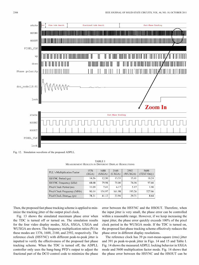
2308 IEEE JOURNAL OF SOLID-STATE CIRCUITS, VOL. 46, NO. 10, OCTOBER 2011
Fig. 12. Simulation waveform of the proposed ADPLL.
TABLE IMEASUREMENT RESULTS IN DIFFERENT DISPLAY RESOLUTIONS
Then, the proposed fast phase tracking scheme is applied tomin-imize the tracking jitter of the output pixel clock.Fig. 13 shows the simulated maximum phase error when
the TDC is turned off or turned on. The simulation resultsfor the four video display modes, XGA, SXGA, UXGA andWUXGA are shown. The frequency multiplication ratios ( ) inthese modes are 1376, 1688, 2160, and 2592, respectively. Thereference clock (HSYNC) with different peak-to-peak jitter isinputted to verify the effectiveness of the proposed fast phasetracking scheme. When the TDC is turned off, the ADPLLcontroller only uses the bang-bang PFD’s output to adjust thefractional part of the DCO control code to minimize the phase
error between the HSYNC and the HSOUT. Therefore, whenthe input jitter is very small, the phase error can be controlledwithin a reasonable range. However, if we keep increasing theinput jitter, the phase error quickly exceeds 100% of the pixelclock period in the WUXGA mode. If the TDC is turned on,the proposed fast phase tracking scheme effectively reduces thephase error in different display resolutions.The reference clock has 39 ps root-mean-square (rms) jitter
and 391 ps peak-to-peak jitter in Figs. 14 and 15 and Table I.Fig. 14 shows the measured ADPLL locking behavior in SXGAmode and 5600 multiplication factor mode. Fig. 14 shows thatthe phase error between the HSYNC and the HSOUT can be

CHUNG AND KO: A FAST PHASE TRACKING ADPLL FOR VIDEO PIXEL CLOCK GENERATION IN 65 NM CMOS TECHNOLOGY 2309
Fig. 13. Maximum phase error when TDC is OFF or ON.
TABLE IIPERFORMANCE COMPARISONS
bounded in steady state even with a very high frequency mul-tiplication ratio. Fig. 15 shows the measured jitter histogramof the output pixel clock in SXGA mode and 5600 multiplica-tion factor mode. The measurement results show that the outputpixel clock has 41.1 ps rms jitter in SXGA mode and 8.64 psrms jitter in SXGA mode, which shows that the period jitter iseffectively reduced by the proposed digital loop filter. The mea-surement results from different display resolutions are summa-rized in Table I. The output period jitter is reduced by the pro-
posed digital loop filter while the tracking jitter is minimized bythe proposed fast phase tracking scheme with the TDC and theDSM.The performance comparisons of the prior studies are listed
in Table II. In [18], a very large frequency multiplication ratio(13,888) is reported, but the proposed frequency counter ar-chitecture can only be used for frequency synthesis applica-tions and not for phase tracking applications. In [15] and [17],two-PLL architecture is used for pixel clock generation applica-

2310 IEEE JOURNAL OF SOLID-STATE CIRCUITS, VOL. 46, NO. 10, OCTOBER 2011
Fig. 14. Measured locking behavior with (a) SXGA mode, and (b) 5600 mul-tiplication factor.
tions, but it requires a large chip area and has high power con-sumption. In addition, an external oscillator increases the costof the design. In [12], the bang-bang PFD without a TDC cannot effectively track the phase of the noisy reference clock, asexplained in Fig. 13. Thus, it is not suitable for pixel clock gen-eration applications.
V. CONCLUSION
In this paper, a fast phase tracking ADPLL for video pixelclock generation in 65 nm CMOS technology is presented. ADCOdithering scheme is applied to improve the frequency reso-lution of the DCO. Thus, the ADPLL can achieve phase trackingeven with a high frequency multiplication ratio ( 800). Whenthe reference clock has large jitter, the proposed digital loopfilter can eliminate the reference clock jitter effects and reducesthe period jitter of the output pixel clock. The proposed fastphase tracking scheme with the TDC and the DSM effectivelyreduces the tracking jitter of the output pixel clock. The max-imum phase error with 1.2 ns peak-to-peak HSYNC jitter in the
Fig. 15. Measured jitter histogram of the pixel clock with (a) SXGAmode, and(b) 5600 multiplication factor.
WUXGA mode is controlled less than 1.7 ns, which is less thanone-third of the output pixel clock period (5.17 ns). The pro-posed ADPLL can perform a precise clock generation from avery noisy and low frequency reference clock. Therefore, it isvery suitable for video pixel clock generation applications in anadvanced CMOS process.
REFERENCES[1] C.-C. Hung and S.-I. Liu, “A leakage-compensated PLL in 65-nm
CMOS technology,” IEEE Trans. Circuits Syst. II: Exp. Briefs, vol.56, no. 7, pp. 525–529, Jul. 2009.
[2] J. G. Maneatis, J. Kim, I. McClatchie, J. Maxey, and M. Shankaradas,“Self-biased high-bandwidth low-jitter 1-to-4096 multiplier clockgenerator PLL,” IEEE J. Solid-State Circuits, vol. 38, no. 11, pp.1795–1803, Nov. 2003.
[3] R. B. Staszewski, D. Leipold, K. Muhammad, and P. T. Balsara, “Dig-ital controlled oscillator (DCO)-based architecture for RF frequencysynthesis in a deep-submicrometer CMOS process,” IEEE Trans.Circuits Syst. II: Analog Digit. Signal Process., vol. 50, no. 11, pp.815–828, Nov. 2003.
[4] P.-H. Hsieh, J. Maxey, and C.-K. K. Yang, “A phase-selecting dig-ital phase-locked loop with bandwidth tracking in 65-nm CMOS tech-nology,” IEEE J. Solid-State Circuits, vol. 45, no. 4, pp. 781–792, Apr.2010.

CHUNG AND KO: A FAST PHASE TRACKING ADPLL FOR VIDEO PIXEL CLOCK GENERATION IN 65 NM CMOS TECHNOLOGY 2311
[5] V. Kratyuk, P. K. Hanumolu, U.-K.Moon, and K.Mayaram, “A designprocedure for all-digital phase-locked loops based on a charge-pumpphase-locked-loop analogy,” IEEE Trans. Circuits Syst. II: Exp. Briefs,vol. 54, no. 3, pp. 247–251, Mar. 2007.
[6] X. Chen, J. Yang, and L.-X. Shi, “A fast locking all-digital phase-locked loop via feed-forward compensation technique,” IEEE Trans.Very Large Scale Integr. (VLSI) Syst., vol. 19, no. 5, pp. 857–868, May2011.
[7] S.-P. Lee and S.-H. Cho, “A background compensation tech-nique for constant bandwidth in all-digital phase-locked loop,” in Proc.2010 IEEE Int. Symp. Circuits and Systems (ISCAS), May 2010, pp.3401–3404.
[8] K.-H. Choi, J.-B. Shin, J.-Y. Sim, and H.-J. Park, “An interpolatingdigitally controlled oscillator for a wide-range all-digital PLL,” IEEETrans. Circuits Syst. I: Reg. Papers, vol. 56, no. 9, pp. 2055–2063, Sep.2009.
[9] S.-Y. Yang, W.-Z. Chen, and T.-Y. Lu, “A 7.1 mW, 10 GHz all digitalfrequency synthesizer with dynamically reconfigured digital loop filterin 90 nm CMOS technology,” IEEE J. Solid-State Circuits, vol. 45, no.3, pp. 578–586, Mar. 2010.
[10] R. B. Staszewski and P. T. Balsara, “All-digital PLL with ultra fastsettling,” IEEE Trans. Circuits Syst. II: Exp. Briefs, vol. 54, no. 2, pp.181–185, Feb. 2007.
[11] C.-C. Hung, I.-F. Chen, and S.-I. Liu, “A 1.25 GHz fast-locked all-dig-ital phase-locked loop with supply noise suppression,” in Proc. 2010IEEE Int. Symp. VLSI Design Automation and Test (VLSI-DAT), Apr.2010, pp. 237–240.
[12] H.-J. Hsu and S.-Y. Huang, “A low-jitter ADPLL via a suppressivedigital filter and an interpolation-based locking scheme,” IEEE Trans.Very Large Scale Integr. (VLSI) Syst., vol. 19, no. 1, pp. 165–170, Jan.2011.
[13] C.-T. Wu, W.-C. Shen, W. Wang, and A.-Y. Wu, “A two-cycle lock-intime ADPLL design based on a frequency estimation algorithm,” IEEETrans. Circuits Syst. II: Exp. Briefs, vol. 57, no. 6, pp. 430–434, Jun.2010.
[14] T.Watanabe and S. Yamauchi, “An all-digital PLL for frequencymulti-plication by 4 to 1022 with seven-cycle lock time,” IEEE J. Solid-StateCircuits, vol. 38, no. 2, pp. 198–204, Feb. 2003.
[15] G.-J. Xie and C.Wang, “An all-digital PLL for video pixel clock regen-eration applications,” in Proc. 2009 World Congr. Computer Scienceand Information Engineering (CSIE), Mar. 2009, pp. 392–396.
[16] T.-Y. Oh, S.-H. Yi, S.-H. Yang, B.-C. Lim, and K.-T. Hong, “A digitalPLL with 5-phase digital PFD for low long-term jitter clock recovery,”in Proc. 2006 IEEE Custom Integrated Circuits Conf. (CICC), Sep.2006, pp. 745–748.
[17] L. Xiu, W. Li, J. Meiners, and R. Padakanti, “A novel all-digital PLLwith software adaptive filter,” IEEE J. Solid-State Circuits, vol. 39, no.3, pp. 476–483, Mar. 2004.
[18] P.-L. Chen, C.-C. Chung, J.-N. Yang, and C.-Y. Lee, “A clock gener-ator with cascaded dynamic frequency counting loops for wide multi-plication range applications,” IEEE J. Solid-State Circuits, vol. 41, no.6, pp. 1275–1285, Jun. 2006.
[19] B.-M. Moon, Y.-J. Park, and D.-K. Jeong, “Monotonic wide-rangedigitally controlled oscillator compensated for supply voltage varia-tion,” IEEE Trans. Circuits Syst. II: Exp. Briefs, vol. 55, no. 10, pp.1036–1040, Oct. 2008.
[20] C.-C. Chung and C.-Y. Lee, “An all-digital phase-locked loop for high-speed clock generation,” IEEE J. Solid-State Circuits, vol. 38, no. 2, pp.347–351, Feb. 2003.
[21] H.-J. Hsu, C.-C. Tu, and S.-Y. Huang, “A high-resolution all-digitalphase-locked loop with its application to built-in speed grading formemory,” in Proc. 2008 IEEE Int. Symp. VLSI Design Automation andTest (VLSI-DAT), Apr. 2008, pp. 267–270.
[22] VESA and Industry Standards and Guidelines for Computer DisplayMonitor Timing, 1.0, Revision 10, Video Electronics Standards Assoc.,2004.
[23] R. B. Staszewski et al., “1.3 V 20 ps time-to-digital converter for fre-quency synthesis in 90-nm CMOS,” IEEE Trans. Circuits Syst. II: Exp.Briefs, vol. 53, no. 3, pp. 220–224, Mar. 2006.
[24] S.-Y. Lin and S.-I. Liu, “A 1.5 GHz all-digital spread-spectrum clockgenerator,” IEEE J. Solid-State Circuits, vol. 44, no. 11, pp. 3111–3119,Nov. 2009.
Ching-Che Chung (S’01–M’03) received the B.S.and Ph.D. degrees in electronics engineering fromNational Chiao-Tung University, Hsinchu, Taiwan,in 1997 and 2003, respectively.From 2004 to 2008, he was serving as a postdoc-
toral researcher in the same university, working inthe area of system-on-chip design methodologies andhigh-speed interface circuit design. In August 2008,he joined the faculty of the Computer Science and In-formation Engineering Department, National ChungCheng University, Chia-Yi, Taiwan, where he is cur-
rently an Assistant Professor. His research interests mainly include wireless andwireline communication systems, low-power and system-on-a-chip (SoC) de-sign technology, mixed-signal IC design and sensor circuits design, all-digitalphase-locked loop, all-digital delay-locked loop and its applications.
Chiun-Yao Ko received the M.S. degree in computerscience and information engineering from NationalChung Cheng University, Chia-Yi, Taiwan, in 2010.He is currently a design engineer at the design
service division of Global Unichip Corporation(GUC), Hsinchu, Taiwan, working on physicaldesign service. His research interests includesystem-on-a-chip (SoC) design methodologies andall-digital phase-locked loop.