2488 ieee journal of solid-state circuits, vol. 46, no. 11
TRANSCRIPT
2488 IEEE JOURNAL OF SOLID-STATE CIRCUITS, VOL. 46, NO. 11, NOVEMBER 2011
Minimized Transient and Steady-State CrossRegulation in 55-nm CMOS Single-Inductor
Dual-Output (SIDO) Step-Down DC-DC ConverterYu-Huei Lee, Student Member, IEEE, Tzu-Chi Huang, Student Member, IEEE, Yao-Yi Yang, Student Member, IEEE,
Wen-Shen Chou, Ke-Horng Chen, Senior Member, IEEE, Chen-Chih Huang, and Ying-Hsi Lin
Abstract—A single-inductor dual-output (SIDO) step-downDC-DC converter with continuous conduction mode (CCM) oper-ation is proposed to achieve an area-efficient power managementmodule. The low-voltage energy distribution controller (LV-EDC)can simultaneously guarantee good voltage regulation and lowoutput voltage ripple. With the proposed dual-mode energy de-livery methodology, cross regulation in steady-state output voltageripple, which is rarely discussed, and cross regulation in loadtransient response are both effectively reduced. In addition, theenergy mode transition operation helps obtain the appropriateenergy operation mode using the energy delivery paths for dualoutputs. Moreover, within the allowable output voltage ripple,the automatic energy bypass (AEB) mechanism can reduce thenumber of energy delivery paths, thereby ensuring voltage regu-lation and further enhancing efficiency. The test chip, fabricatedin 55-nm CMOS, occupies 1.44 mm and achieves 91% peakefficiency, low output voltage ripple, and excellent load transientresponse for a high-efficiency system-on-a-chip (SoC) integration.
Index Terms—Cross regulation, energy bypass mechanism, en-ergy delivery path, load transient response, output voltage ripple,power conversion efficiency, single-inductor dual-output (SIDO)converter.
I. INTRODUCTION
S INGLE-INDUCTOR dual-output (SIDO) converter[1]–[14] can be used to power the different function
blocks to achieve the battery-operated system-on-a-chip (SoC)integration. With the use of a single off-chip inductor, the SIDOconverter can allocate energy to dual outputs and provide twoindependent supply voltages. As a result, the print-circuit-board(PCB) area can be effectively reduced since the conventionalpower management modules [15]–[18] require two inductorsto generate dual outputs. Low output voltage ripple, minimizedcross regulation, and high power conversion efficiency areessential design issues for a SIDO converter. Fig. 1 shows the
Manuscript received February 17, 2011; revised May 10, 2011; accepted July20, 2011. Date of publication September 12, 2011; date of current version Oc-tober 26, 2011. This paper was approved by Guest Editor Muneo Fukaishi. Thiswork was supported by the National Science Council, Taiwan, under Grant NSC100-2220-E-009-050 and Grant NSC 100-2220-E-009-055.Y.-H. Lee, T.-C. Huang, Y.-Y. Yang, W.-S. Chou, and K.-H. Chen are with
the Institute of Electrical Control Engineering, National Chiao Tung University,30010 Hsinchu, Taiwan (e-mail: [email protected]).C.-C. Huang and Y.-H. Lin are with the Realtek Semiconductor Corporation,
Hsinchu, Taiwan.Color versions of one or more of the figures in this paper are available online
at http://ieeexplore.ieee.org.Digital Object Identifier 10.1109/JSSC.2011.2164019
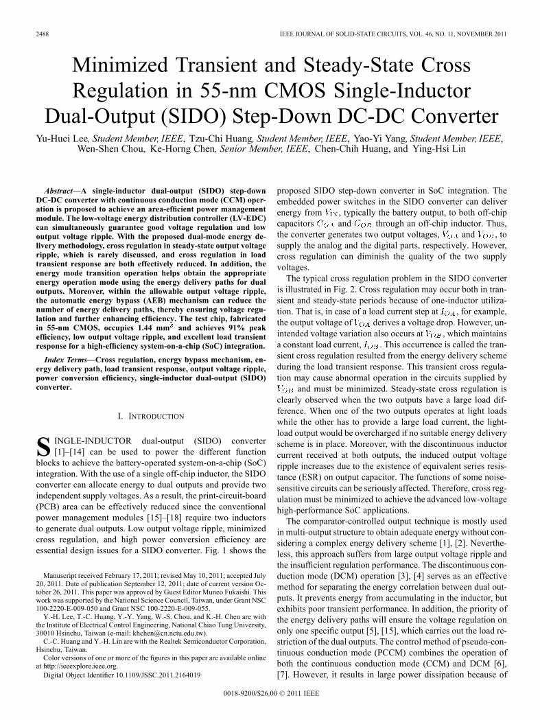
proposed SIDO step-down converter in SoC integration. Theembedded power switches in the SIDO converter can deliverenergy from , typically the battery output, to both off-chipcapacitors and through an off-chip inductor. Thus,the converter generates two output voltages, and , tosupply the analog and the digital parts, respectively. However,cross regulation can diminish the quality of the two supplyvoltages.The typical cross regulation problem in the SIDO converter
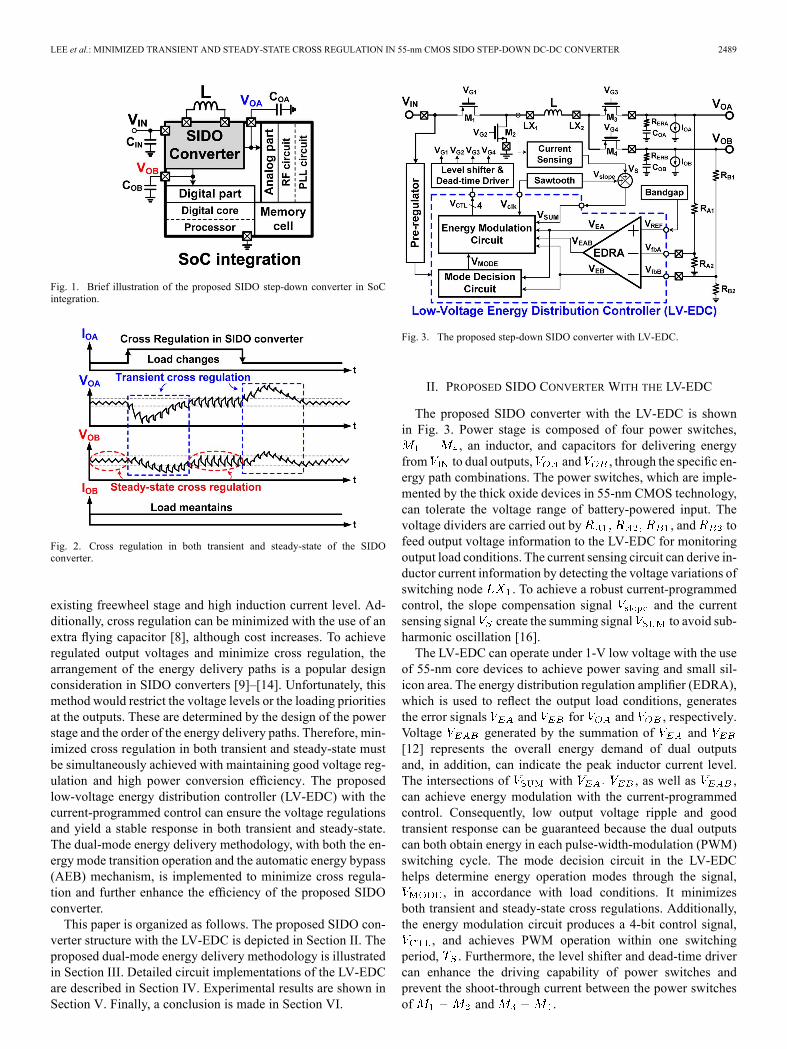
is illustrated in Fig. 2. Cross regulation may occur both in tran-sient and steady-state periods because of one-inductor utiliza-tion. That is, in case of a load current step at , for example,the output voltage of derives a voltage drop. However, un-intended voltage variation also occurs at , which maintainsa constant load current, . This occurrence is called the tran-sient cross regulation resulted from the energy delivery schemeduring the load transient response. This transient cross regula-tion may cause abnormal operation in the circuits supplied by
and must be minimized. Steady-state cross regulation isclearly observed when the two outputs have a large load dif-ference. When one of the two outputs operates at light loadswhile the other has to provide a large load current, the light-load output would be overcharged if no suitable energy deliveryscheme is in place. Moreover, with the discontinuous inductorcurrent received at both outputs, the induced output voltageripple increases due to the existence of equivalent series resis-tance (ESR) on output capacitor. The functions of some noise-sensitive circuits can be seriously affected. Therefore, cross reg-ulation must be minimized to achieve the advanced low-voltagehigh-performance SoC applications.The comparator-controlled output technique is mostly used
in multi-output structure to obtain adequate energy without con-sidering a complex energy delivery scheme [1], [2]. Neverthe-less, this approach suffers from large output voltage ripple andthe insufficient regulation performance. The discontinuous con-duction mode (DCM) operation [3], [4] serves as an effectivemethod for separating the energy correlation between dual out-puts. It prevents energy from accumulating in the inductor, butexhibits poor transient performance. In addition, the priority ofthe energy delivery paths will ensure the voltage regulation ononly one specific output [5], [15], which carries out the load re-striction of the dual outputs. The control method of pseudo-con-tinuous conduction mode (PCCM) combines the operation ofboth the continuous conduction mode (CCM) and DCM [6],[7]. However, it results in large power dissipation because of
0018-9200/$26.00 © 2011 IEEE
LEE et al.: MINIMIZED TRANSIENT AND STEADY-STATE CROSS REGULATION IN 55-nm CMOS SIDO STEP-DOWN DC-DC CONVERTER 2489
Fig. 1. Brief illustration of the proposed SIDO step-down converter in SoCintegration.
Fig. 2. Cross regulation in both transient and steady-state of the SIDOconverter.
existing freewheel stage and high induction current level. Ad-ditionally, cross regulation can be minimized with the use of anextra flying capacitor [8], although cost increases. To achieveregulated output voltages and minimize cross regulation, thearrangement of the energy delivery paths is a popular designconsideration in SIDO converters [9]–[14]. Unfortunately, thismethod would restrict the voltage levels or the loading prioritiesat the outputs. These are determined by the design of the powerstage and the order of the energy delivery paths. Therefore, min-imized cross regulation in both transient and steady-state mustbe simultaneously achieved with maintaining good voltage reg-ulation and high power conversion efficiency. The proposedlow-voltage energy distribution controller (LV-EDC) with thecurrent-programmed control can ensure the voltage regulationsand yield a stable response in both transient and steady-state.The dual-mode energy delivery methodology, with both the en-ergy mode transition operation and the automatic energy bypass(AEB) mechanism, is implemented to minimize cross regula-tion and further enhance the efficiency of the proposed SIDOconverter.This paper is organized as follows. The proposed SIDO con-
verter structure with the LV-EDC is depicted in Section II. Theproposed dual-mode energy delivery methodology is illustratedin Section III. Detailed circuit implementations of the LV-EDCare described in Section IV. Experimental results are shown inSection V. Finally, a conclusion is made in Section VI.
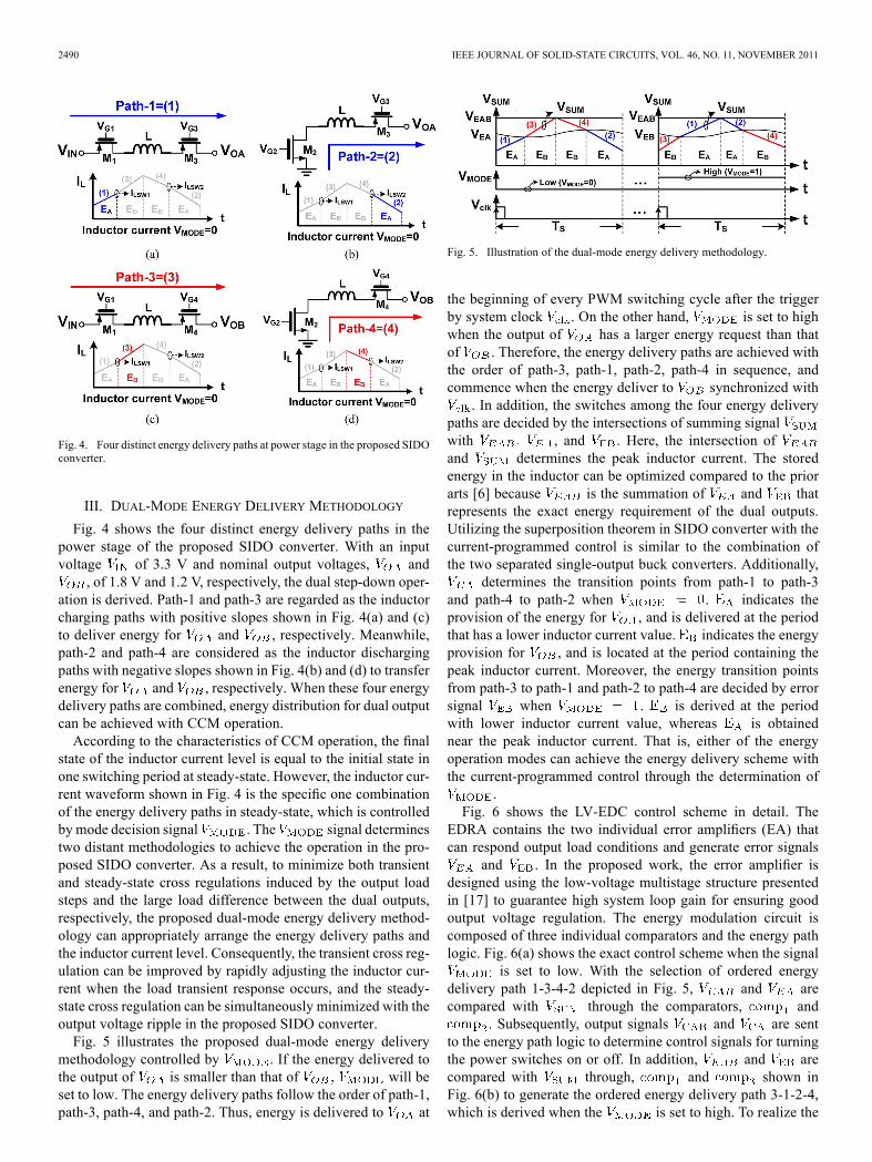
Fig. 3. The proposed step-down SIDO converter with LV-EDC.
II. PROPOSED SIDO CONVERTER WITH THE LV-EDC
The proposed SIDO converter with the LV-EDC is shownin Fig. 3. Power stage is composed of four power switches,
, an inductor, and capacitors for delivering energyfrom to dual outputs, and , through the specific en-ergy path combinations. The power switches, which are imple-mented by the thick oxide devices in 55-nm CMOS technology,can tolerate the voltage range of battery-powered input. Thevoltage dividers are carried out by , and tofeed output voltage information to the LV-EDC for monitoringoutput load conditions. The current sensing circuit can derive in-ductor current information by detecting the voltage variations ofswitching node . To achieve a robust current-programmedcontrol, the slope compensation signal and the currentsensing signal create the summing signal to avoid sub-harmonic oscillation [16].The LV-EDC can operate under 1-V low voltage with the use
of 55-nm core devices to achieve power saving and small sil-icon area. The energy distribution regulation amplifier (EDRA),which is used to reflect the output load conditions, generatesthe error signals and for and , respectively.Voltage generated by the summation of and[12] represents the overall energy demand of dual outputsand, in addition, can indicate the peak inductor current level.The intersections of with , as well as ,can achieve energy modulation with the current-programmedcontrol. Consequently, low output voltage ripple and goodtransient response can be guaranteed because the dual outputscan both obtain energy in each pulse-width-modulation (PWM)switching cycle. The mode decision circuit in the LV-EDChelps determine energy operation modes through the signal,
, in accordance with load conditions. It minimizesboth transient and steady-state cross regulations. Additionally,the energy modulation circuit produces a 4-bit control signal,
, and achieves PWM operation within one switchingperiod, . Furthermore, the level shifter and dead-time drivercan enhance the driving capability of power switches andprevent the shoot-through current between the power switchesof and .
2490 IEEE JOURNAL OF SOLID-STATE CIRCUITS, VOL. 46, NO. 11, NOVEMBER 2011
Fig. 4. Four distinct energy delivery paths at power stage in the proposed SIDOconverter.
III. DUAL-MODE ENERGY DELIVERY METHODOLOGY
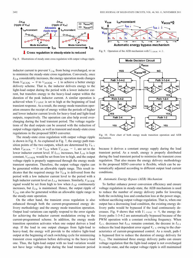
Fig. 4 shows the four distinct energy delivery paths in thepower stage of the proposed SIDO converter. With an inputvoltage of 3.3 V and nominal output voltages, and
, of 1.8 V and 1.2 V, respectively, the dual step-down oper-ation is derived. Path-1 and path-3 are regarded as the inductorcharging paths with positive slopes shown in Fig. 4(a) and (c)to deliver energy for and , respectively. Meanwhile,path-2 and path-4 are considered as the inductor dischargingpaths with negative slopes shown in Fig. 4(b) and (d) to transferenergy for and , respectively. When these four energydelivery paths are combined, energy distribution for dual outputcan be achieved with CCM operation.According to the characteristics of CCM operation, the final
state of the inductor current level is equal to the initial state inone switching period at steady-state. However, the inductor cur-rent waveform shown in Fig. 4 is the specific one combinationof the energy delivery paths in steady-state, which is controlledby mode decision signal . The signal determinestwo distant methodologies to achieve the operation in the pro-posed SIDO converter. As a result, to minimize both transientand steady-state cross regulations induced by the output loadsteps and the large load difference between the dual outputs,respectively, the proposed dual-mode energy delivery method-ology can appropriately arrange the energy delivery paths andthe inductor current level. Consequently, the transient cross reg-ulation can be improved by rapidly adjusting the inductor cur-rent when the load transient response occurs, and the steady-state cross regulation can be simultaneously minimized with theoutput voltage ripple in the proposed SIDO converter.Fig. 5 illustrates the proposed dual-mode energy delivery
methodology controlled by . If the energy delivered tothe output of is smaller than that of will beset to low. The energy delivery paths follow the order of path-1,path-3, path-4, and path-2. Thus, energy is delivered to at
Fig. 5. Illustration of the dual-mode energy delivery methodology.
the beginning of every PWM switching cycle after the triggerby system clock . On the other hand, is set to highwhen the output of has a larger energy request than thatof . Therefore, the energy delivery paths are achieved withthe order of path-3, path-1, path-2, path-4 in sequence, andcommence when the energy deliver to synchronized with
. In addition, the switches among the four energy deliverypaths are decided by the intersections of summing signalwith , and . Here, the intersection ofand determines the peak inductor current. The storedenergy in the inductor can be optimized compared to the priorarts [6] because is the summation of and thatrepresents the exact energy requirement of the dual outputs.Utilizing the superposition theorem in SIDO converter with thecurrent-programmed control is similar to the combination ofthe two separated single-output buck converters. Additionally,
determines the transition points from path-1 to path-3and path-4 to path-2 when . indicates theprovision of the energy for , and is delivered at the periodthat has a lower inductor current value. indicates the energyprovision for , and is located at the period containing thepeak inductor current. Moreover, the energy transition pointsfrom path-3 to path-1 and path-2 to path-4 are decided by errorsignal when . is derived at the periodwith lower inductor current value, whereas is obtainednear the peak inductor current. That is, either of the energyoperation modes can achieve the energy delivery scheme withthe current-programmed control through the determination of
.Fig. 6 shows the LV-EDC control scheme in detail. The
EDRA contains the two individual error amplifiers (EA) thatcan respond output load conditions and generate error signals
and . In the proposed work, the error amplifier isdesigned using the low-voltage multistage structure presentedin [17] to guarantee high system loop gain for ensuring goodoutput voltage regulation. The energy modulation circuit iscomposed of three individual comparators and the energy pathlogic. Fig. 6(a) shows the exact control scheme when the signal
is set to low. With the selection of ordered energydelivery path 1-3-4-2 depicted in Fig. 5, and arecompared with through the comparators, and
. Subsequently, output signals and are sentto the energy path logic to determine control signals for turningthe power switches on or off. In addition, and arecompared with through, and shown inFig. 6(b) to generate the ordered energy delivery path 3-1-2-4,which is derived when the is set to high. To realize the

LEE et al.: MINIMIZED TRANSIENT AND STEADY-STATE CROSS REGULATION IN 55-nm CMOS SIDO STEP-DOWN DC-DC CONVERTER 2491
Fig. 6. Control scheme of the LV-EDC circuit. (a) The operation of. (a) The operation of .
energy delivery paths, the energy path logic can determine the4-bit control signal, , with the synchronization of forachieving the energy delivery methodology.Moreover, to further enhance both transient and steady-state
cross regulations, the energy delivery paths must be optimizedin accordance with the output load conditions. That is, the en-ergy operation mode and the energy delivery paths must be ad-justed accordingly to obtain suitable energy delivery scheme fordual outputs.
A. Energy Mode Transition Operation
Output voltage ripples and in the proposed SIDOconverter are illustrated, respectively, as
(1)
(2)
where
(3)
and are the equivalent load resistances at and, respectively. and indicate the turned-on
periods of the power switches, and , respectively.and are the ESRs on output capacitors andrespectively. From the equations shown in (1) and (2), the firstterm in both (1) and (2) contain the output voltage values, loadconditions, and output capacitor values. These factors are alllimited by design specifications. As depicted in (3), isthe maximum value between the currents of anddepicted in Fig. 4. represents the exact inductor currentvalue at the energy path transition point, where and
Fig. 7. Energy mode transition operation during the load transient response.
or and intersect in different energy operation modes.In addition, the power switches and are used to allocateenergy for the dual outputs, both of which, however, cannot re-ceive energy simultaneously owing to the SIDO methodology.Thus, the discontinuous inductor current is certainly derived atboth outputs, and thereby the output voltage ripple is affectedby the ESR and the current . As shown in (1) and (2), thelower output voltage ripples are generated through the reductionof the value. In other words, given the material-depen-dent value of ESR, minimizing the current can helps re-duce the output voltage ripples, as well as the steady-state crossregulation. That is, although the first terms in both (1) and (2)cannot be alleviated due to the design specifications, the energymode transition operation can help get lower to furtherreduce the output voltage ripple.The superposition theorem can achieve the operation in pro-
posed SIDO converter without the need of freewheel stage, andcan reduce the inductor current level to obtain smalleras well as output voltage ripples. However, when a large loaddifference occurs between the dual outputs, the output voltageripple may increase because of the increase in . For ex-ample, if is considerably larger than and theis set to low, the area shown in Fig. 5 would occupy mostof the energy transition period in one switching cycle. That is,
and the output voltage ripple will increase. This phenom-enon, which is considered as the steady-state cross regulation,is resulted from the unchanged energy delivery scheme that the
is set to low. This energy operationmode cannot operatewell in such as the load condition. Therefore, the combinationand duration of the energy delivery paths must be adjusted ac-cording to the output load conditions.The energy mode transient operation of the proposed SIDO
converter is shown in Fig. 7. Assuming that is initiallyset to low, the increase in leads to the increase in the in-ductor current with the extension of energy delivery period for
to acquire more power. The energy delivery mode mustbe maintained because of the remained loading of . Thus,the energy path transition point is set to the lower side of the
2492 IEEE JOURNAL OF SOLID-STATE CIRCUITS, VOL. 46, NO. 11, NOVEMBER 2011
Fig. 8. Illustrations of steady-state cross regulation with output voltage ripple.
inductor current to prevent from being overcharged, so asto minimize the steady-state cross regulation. Conversely, once
considerably increases, the energy operation mode changesfrom to to achieve a better energydelivery scheme. That is, the inductor delivers energy to thelight-load output during the period with a lower inductor cur-rent, but transfers energy to the heavy-load output within theduration of the peak inductor current. A similar operation isachieved when is set to high at the beginning of loadtransient response. As a result, the energy mode transition oper-ation ensures the receipt of energy within the periods of higherand lower inductor current levels for heavy-load and light-loadoutputs, respectively. The operation can also help avoid over-charging during the load transient period. The voltage regula-tions of the dual outputs can be assured with the reduction ofoutput voltage ripples, as well as transient and steady-state crossregulations in the proposed SIDO converter.The steady-state cross regulation with output voltage ripple
is shown in Fig. 8. As explained in Fig. 7, the energy path tran-sition points of the two outputs, which are determined bywhen or when , are set to thelower inductor current level. If increases, but is keptconstant, would be set from low to high, and the outputvoltage ripple is properly suppressed through the energy modetransient operation. Therefore, the output voltage ripples canbe generated within an allowable ripple range. This result in-dicates that the required energy for is delivered from theperiod with a low inductor current level to the period with ahigh inductor current level as increases. Similarly,signal would be set from high to low when continuouslyincreases, but is maintained. Hence, the output ripple of
can also be generated within an allowable ripple range inthe steady-state operation.On the other hand, the transient cross regulation is also
enhanced through both the current-programmed energy de-livery methodology and the energy mode transition operation.Output load variations can rapidly respond to the error signalsfor achieving the inductor current modulation owing to thecurrent-programmed scheme. In addition, the energy modetransition operation activates when one output derives a loadstep. If the load in one output changes from light-load toheavy-load, the energy will provide to the relative light-loadoutput at the beginning of each switching cycle for minimizingtransient cross regulation before delivering to the heavy-loadone. Thus, the light-load output with no load variation wouldnot have large voltage drop during the load transient period
Fig. 9. Operation of the AEB mechanism with .
Fig. 10. Flow chart of both energy mode transition operation and AEBmechanism.
because it derives a constant energy supply during the loadtransient period. As a result, energy is properly distributedduring the load transient period to minimize the transient crossregulation. That also means the energy delivery methodologyin the proposed SIDO converter is flexible, which can be au-tomatically adjusted according to different output load currentconditions.
B. Automatic Energy Bypass (AEB) Mechanism
To further enhance power conversion efficiency and ensurevoltage regulation in steady-state, the AEB mechanism is usedto reduce the number of energy delivery paths for loweringboth the switching loss and conduction loss at the power stage,without sacrificing output voltage regulation. That is, when oneoutput has a decreasing load condition, the existing energy de-livery paths would be bypassed if the load continuously de-creases. Fig. 9 shows that with , the energy de-livery paths 1-3-4-2 are automatically bypassed because of thePWM operation with a constant switching frequency. When
decreases but remains constant, the decease inreduces the load dependent error signal owing to the char-acteristics of current-programmed control. As a result, path-1is bypassed first to reduce the duration of energy delivery for
. The maintained three energy delivery paths can ensurevoltage regulation that the light-load output is not overchargedin steady-state, and the output voltage ripple is still maintained
LEE et al.: MINIMIZED TRANSIENT AND STEADY-STATE CROSS REGULATION IN 55-nm CMOS SIDO STEP-DOWN DC-DC CONVERTER 2493
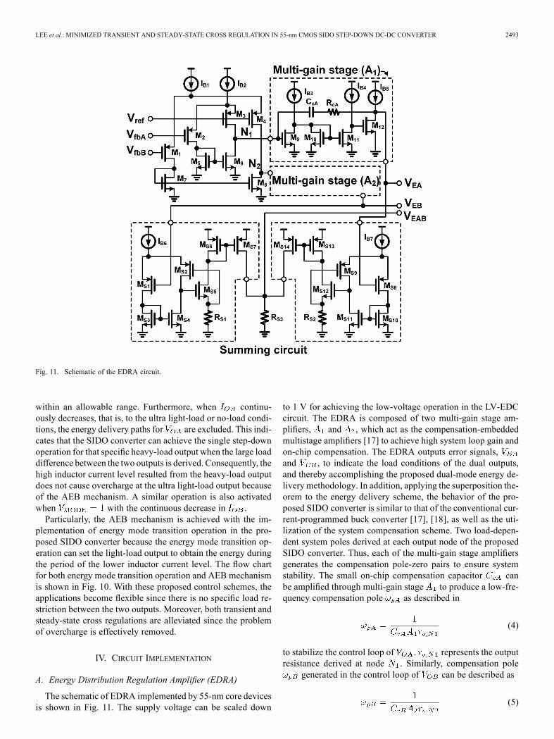
Fig. 11. Schematic of the EDRA circuit.
within an allowable range. Furthermore, when continu-ously decreases, that is, to the ultra light-load or no-load condi-tions, the energy delivery paths for are excluded. This indi-cates that the SIDO converter can achieve the single step-downoperation for that specific heavy-load output when the large loaddifference between the two outputs is derived. Consequently, thehigh inductor current level resulted from the heavy-load outputdoes not cause overcharge at the ultra light-load output becauseof the AEB mechanism. A similar operation is also activatedwhen with the continuous decrease in .Particularly, the AEB mechanism is achieved with the im-
plementation of energy mode transition operation in the pro-posed SIDO converter because the energy mode transition op-eration can set the light-load output to obtain the energy duringthe period of the lower inductor current level. The flow chartfor both energy mode transition operation and AEB mechanismis shown in Fig. 10. With these proposed control schemes, theapplications become flexible since there is no specific load re-striction between the two outputs. Moreover, both transient andsteady-state cross regulations are alleviated since the problemof overcharge is effectively removed.
IV. CIRCUIT IMPLEMENTATION
A. Energy Distribution Regulation Amplifier (EDRA)
The schematic of EDRA implemented by 55-nm core devicesis shown in Fig. 11. The supply voltage can be scaled down
to 1 V for achieving the low-voltage operation in the LV-EDCcircuit. The EDRA is composed of two multi-gain stage am-plifiers, and , which act as the compensation-embeddedmultistage amplifiers [17] to achieve high system loop gain andon-chip compensation. The EDRA outputs error signals,and , to indicate the load conditions of the dual outputs,and thereby accomplishing the proposed dual-mode energy de-livery methodology. In addition, applying the superposition the-orem to the energy delivery scheme, the behavior of the pro-posed SIDO converter is similar to that of the conventional cur-rent-programmed buck converter [17], [18], as well as the uti-lization of the system compensation scheme. Two load-depen-dent system poles derived at each output node of the proposedSIDO converter. Thus, each of the multi-gain stage amplifiersgenerates the compensation pole-zero pairs to ensure systemstability. The small on-chip compensation capacitor canbe amplified through multi-gain stage to produce a low-fre-quency compensation pole as described in
(4)
to stabilize the control loop of . represents the outputresistance derived at node . Similarly, compensation pole
generated in the control loop of can be described as
(5)
2494 IEEE JOURNAL OF SOLID-STATE CIRCUITS, VOL. 46, NO. 11, NOVEMBER 2011
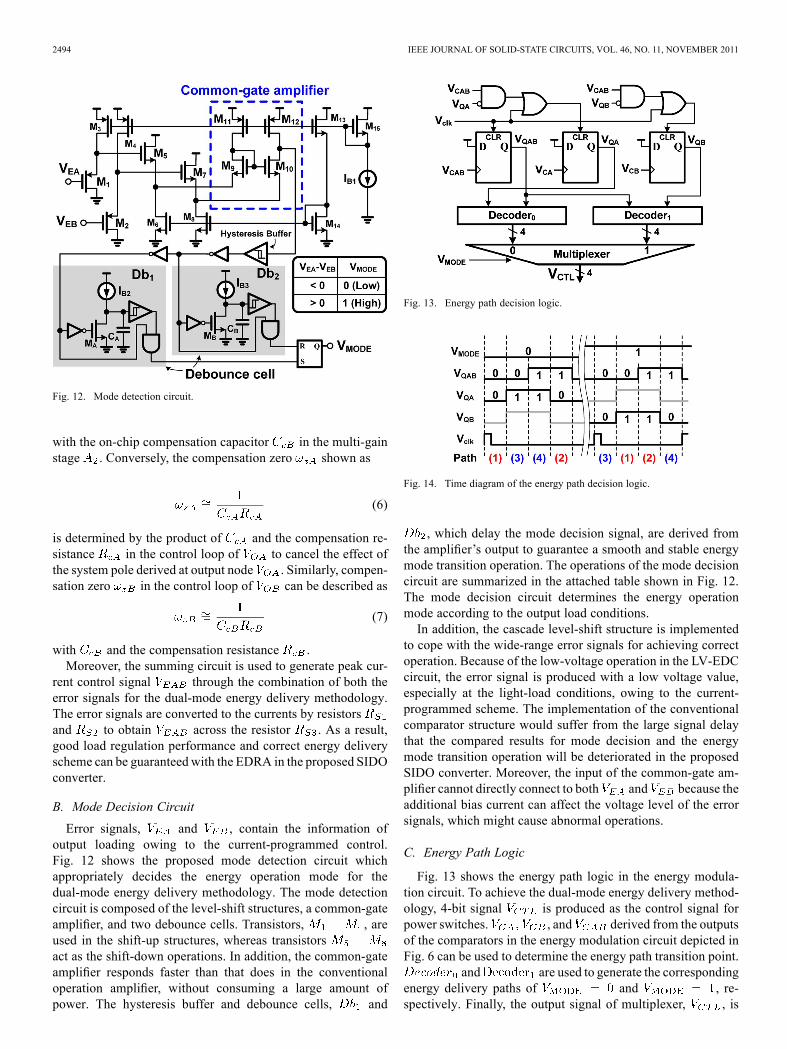
Fig. 12. Mode detection circuit.
with the on-chip compensation capacitor in the multi-gainstage . Conversely, the compensation zero shown as
(6)
is determined by the product of and the compensation re-sistance in the control loop of to cancel the effect ofthe system pole derived at output node . Similarly, compen-sation zero in the control loop of can be described as
(7)
with and the compensation resistance .Moreover, the summing circuit is used to generate peak cur-
rent control signal through the combination of both theerror signals for the dual-mode energy delivery methodology.The error signals are converted to the currents by resistorsand to obtain across the resistor . As a result,good load regulation performance and correct energy deliveryscheme can be guaranteed with the EDRA in the proposed SIDOconverter.
B. Mode Decision Circuit
Error signals, and , contain the information ofoutput loading owing to the current-programmed control.Fig. 12 shows the proposed mode detection circuit whichappropriately decides the energy operation mode for thedual-mode energy delivery methodology. The mode detectioncircuit is composed of the level-shift structures, a common-gateamplifier, and two debounce cells. Transistors, , areused in the shift-up structures, whereas transistorsact as the shift-down operations. In addition, the common-gateamplifier responds faster than that does in the conventionaloperation amplifier, without consuming a large amount ofpower. The hysteresis buffer and debounce cells, and
Fig. 13. Energy path decision logic.
Fig. 14. Time diagram of the energy path decision logic.
, which delay the mode decision signal, are derived fromthe amplifier’s output to guarantee a smooth and stable energymode transition operation. The operations of the mode decisioncircuit are summarized in the attached table shown in Fig. 12.The mode decision circuit determines the energy operationmode according to the output load conditions.In addition, the cascade level-shift structure is implemented
to cope with the wide-range error signals for achieving correctoperation. Because of the low-voltage operation in the LV-EDCcircuit, the error signal is produced with a low voltage value,especially at the light-load conditions, owing to the current-programmed scheme. The implementation of the conventionalcomparator structure would suffer from the large signal delaythat the compared results for mode decision and the energymode transition operation will be deteriorated in the proposedSIDO converter. Moreover, the input of the common-gate am-plifier cannot directly connect to both and because theadditional bias current can affect the voltage level of the errorsignals, which might cause abnormal operations.
C. Energy Path Logic
Fig. 13 shows the energy path logic in the energy modula-tion circuit. To achieve the dual-mode energy delivery method-ology, 4-bit signal is produced as the control signal forpower switches. , and derived from the outputsof the comparators in the energy modulation circuit depicted inFig. 6 can be used to determine the energy path transition point.
and are used to generate the correspondingenergy delivery paths of and , re-spectively. Finally, the output signal of multiplexer, , is

LEE et al.: MINIMIZED TRANSIENT AND STEADY-STATE CROSS REGULATION IN 55-nm CMOS SIDO STEP-DOWN DC-DC CONVERTER 2495
Fig. 15. Measured steady-state operation with both mA andmA when is 3.3 V. (a) with path 1-3-4-2.
(b) with path 3-1-2-4.
selected through the signal to realize the dual-mode en-ergy delivery methodology. The timing diagram of the energypath logic is shown in Fig. 14.
V. EXPERIMENTAL RESULTS
The proposed SIDO converter with the LV-EDC was fabri-cated in 55-nm CMOS technology. The nominal output volt-ages of and are 1.8 V and 1.2 V, respectively. Fig. 15shows the measured steady-state operation with load currentsof 100 mA at the two outputs, and . Fig. 15(a) demon-strates the ordered energy delivery paths with path 1-3-4-2 insequence when is set to low. The average inductor cur-rent is 200 mA, which is equal to the summation of the twooutput loads. The output voltage ripples are derived with 20 mVand 22 mV at and , respectively. Fig. 15(b) showsthe energy delivery scheme with path 3-1-2-4 when isset to high. The output voltage ripples are kept within 24 mVand 20 mV, respectively. That is, the energy delivery schemecan be achieved with either of the two energy operation modeswhen no large load difference exists between the dual outputs.Fig. 16 shows the measured waveforms with and of120 mA and 60 mA, respectively. Fig. 16(a) shows the mea-sured result with forcing to low. The light-load output
is obtained energy within the period containing the peakinductor current. Thus, the voltage ripples of andare 25 mV and 40 mV, respectively, indicating that the light-load output suffers from the steady-state cross regulation dueto the incorrect utilization of the energy operation mode. For-tunately, with the operation of mode decision circuit shown inFig. 16(b), the voltage ripple of is reduced to 20 mV, while
Fig. 16. Measured steady-state operation with both mA andmA when is 3.3 V. (a) with path 1-3-4-2.
(b) with path 3-1-2-4.
Fig. 17. Measured AEBmechanism under different load conditions whenis 3.3 V. (a) mA and mAwith . (b)
mA and mA with .
the voltage ripple of is retained at 25 mV when ischanged to high. This result demonstrates the suppression of the

2496 IEEE JOURNAL OF SOLID-STATE CIRCUITS, VOL. 46, NO. 11, NOVEMBER 2011
Fig. 18. Measured load transient response with energy mode transitionoperation.
Fig. 19. Measured line transient response of a 0.2 V voltage step at withmA and mA.
steady-state cross regulation in the proposed SIDO converter.Fig. 17 shows the measured AEB mechanism. When isset to low, the decrease in activates the AEB mechanismto bypass the energy delivery path to enhance efficiency andensure voltage regulation. As shown in Fig. 17(a), the energypath is reduced to path 3-4-2 in one PWM switching cycle when
and are 50 mA and 100 mA, respectively. Therefore,the switching loss can be reduced while voltage regulation isstill guaranteed. Moreover, Fig. 17(b) shows the ultra light-loadcondition of . Through the proposed AEB mechanism, theSIDO converter can operate the single step-down operation for
unless requires energy replenishment. As a result, nominimum loading restriction occurs at each output in the pro-posed SIDO converter.Fig. 18 shows the measured load transient response. The load
currents are initially set to 60 mA for each output at. When is suddenly changed from 60 mA to 240 mA,the energy operation mode is changed to obtain a better energydelivery scheme, which realizes the energy delivery period of
including the peak inductor current. Subsequently, whenincreases from 60 mA to 240 mA and is maintained
at 240 mA, the energy operation mode is once again changedthrough the energy mode transient operation. Therefore, bothtransient and steady-state cross regulations can be minimized.The largest voltage variation is near 100 mV and the voltagerecovery time is shorter than 30 s. Particularly, the final stateof the measured load transient response is identical to that in theinitial state. That is, the final state derives the 60mA load at each
Fig. 20. Measured output voltage ripple. (a) Output ripple of . (b) Outputripple of .
Fig. 21. Chip micrograph of the proposed SIDO converter.
Fig. 22. Measured power conversion efficiency with V,V, and V.
output, but operates with the distinct energy operation modecompared to initial state. This result is caused by the hysteresisbuffer in the mode decision circuit. Nevertheless, either of theenergy operation modes can be utilized when the two outputloads are closed as demonstrated in Fig. 16. Fig. 19 shows themeasured line transient response. When has a voltage stepof 200 mV within 40 s, the dual output voltages derive theinduced voltage variations, which are smaller than 50 mV.Fig. 20 shows the measured output voltage ripple. Through
the energy mode transition operation and the AEB mechanism,
LEE et al.: MINIMIZED TRANSIENT AND STEADY-STATE CROSS REGULATION IN 55-nm CMOS SIDO STEP-DOWN DC-DC CONVERTER 2497
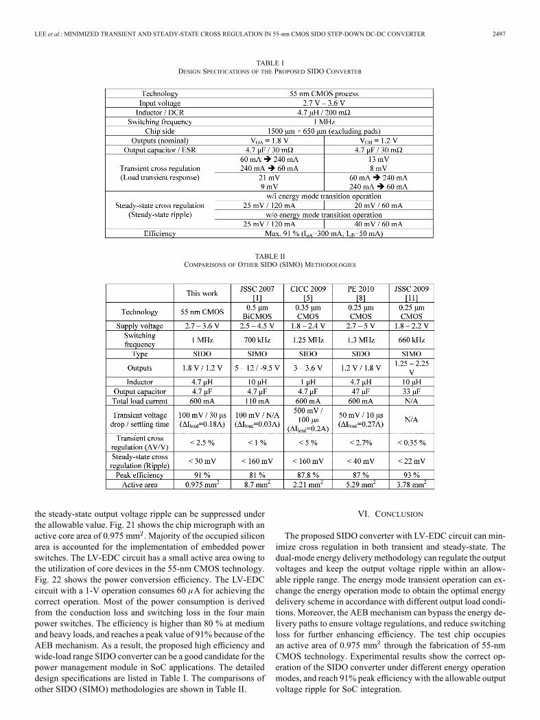
TABLE IDESIGN SPECIFICATIONS OF THE PROPOSED SIDO CONVERTER
TABLE IICOMPARISONS OF OTHER SIDO (SIMO) METHODOLOGIES
the steady-state output voltage ripple can be suppressed underthe allowable value. Fig. 21 shows the chip micrograph with anactive core area of 0.975 mm . Majority of the occupied siliconarea is accounted for the implementation of embedded powerswitches. The LV-EDC circuit has a small active area owing tothe utilization of core devices in the 55-nm CMOS technology.Fig. 22 shows the power conversion efficiency. The LV-EDCcircuit with a 1-V operation consumes 60 A for achieving thecorrect operation. Most of the power consumption is derivedfrom the conduction loss and switching loss in the four mainpower switches. The efficiency is higher than 80 % at mediumand heavy loads, and reaches a peak value of 91% because of theAEB mechanism. As a result, the proposed high efficiency andwide-load range SIDO converter can be a good candidate for thepower management module in SoC applications. The detaileddesign specifications are listed in Table I. The comparisons ofother SIDO (SIMO) methodologies are shown in Table II.
VI. CONCLUSION
The proposed SIDO converter with LV-EDC circuit can min-imize cross regulation in both transient and steady-state. Thedual-mode energy delivery methodology can regulate the outputvoltages and keep the output voltage ripple within an allow-able ripple range. The energy mode transient operation can ex-change the energy operation mode to obtain the optimal energydelivery scheme in accordance with different output load condi-tions. Moreover, the AEBmechanism can bypass the energy de-livery paths to ensure voltage regulations, and reduce switchingloss for further enhancing efficiency. The test chip occupiesan active area of 0.975 mm through the fabrication of 55-nmCMOS technology. Experimental results show the correct op-eration of the SIDO converter under different energy operationmodes, and reach 91% peak efficiency with the allowable outputvoltage ripple for SoC integration.

2498 IEEE JOURNAL OF SOLID-STATE CIRCUITS, VOL. 46, NO. 11, NOVEMBER 2011
ACKNOWLEDGMENT
The authors wish to thank Energy Pass Incorporation for theirhelp.
REFERENCES
[1] H.-P. Le, C.-S. Chae, K.-C. Lee, S.-W. Wang, G.-H. Cho, and G.-H.Cho, “A single-inductor switching DC-DC converter with five outputsand ordered power-distributive control,” IEEE J. Solid-State Circuits,vol. 42, no. 12, pp. 2076–2714, Dec. 2007.
[2] K.-S. Seol, Y.-J. Woo, G.-H. Cho, G.-H. Cho, J.-W. Lee, and S.-I. Kim,“Multiple-output step-up/down switching dc-dc converter with vesti-gial current control,” in IEEE ISSCC Dig. Tech. Papers, Feb. 2009, pp.442–443.
[3] D. Kwon and G. A. Rincón-Mora, “Single-inductor-multiple-outputswitching DC-DC converters,” IEEE Trans. Circuits Syst. II, Exp.Briefs, vol. 56, no. 8, pp. 614–618, Aug. 2009.
[4] E. Bonizzoni, F. Borghetti, P. Malcovati, F. Maloberti, and B. Niessen,“A 200 mA 93% peak efficiency single-inductor dual-output DC-DCbuck converter,” in IEEE ISSCC Dig. Tech. Papers, Feb. 2007, pp.526–527.
[5] X. Jing, P. K. T. Mok, and M. C. Lee, “A wide-load-range single-in-ductor dual-output boost regulator with minimized cross-regulationby constant-charge-auto-hopping (CCAH) control,” in Proc. IEEECustom Integrated Circuits Conf. (CICC), Sep. 2009, pp. 299–302.
[6] D. Ma, W.-H. Ki, and C.-Y. Tsui, “A pseudo-CCM/DCM SIMOswitching converter with freewheel switching,” IEEE J. Solid-StateCircuits, vol. 38, no. 6, pp. 1007–1014, Jun. 2003.
[7] Y.-J. Woo, H.-P. Le, G.-H. Cho, G.-H. Cho, and S.-I. Kim, “Load-independent control of switching DC-DC converters with freewheelingcurrent feedback,” IEEE J. Solid-State Circuits, vol. 43, no. 12, pp.2798–2808, Dec. 2008.
[8] W.Xu, Y. Li, X. Gong, Z. Hong, andD. Killat, “A dual-mode single-in-ductor dual-output switching converter with small ripple,” IEEE Trans.Power Electron., vol. 25, no. 3, pp. 614–623, Mar. 2010.
[9] M.-H. Huang and K.-H. Chen, “Single-inductor dual buck-boostoutput (SIDBBO) converter adaptive current control mode (ACCM)and adaptive body switch (ABS) for compact size and long battery lifein portable devices,” in Proc. IEEE Symp. VLSI Circuits, Jun. 2009,pp. 164–165.
[10] C.-S. Chae, H.-P. Le, K.-C. Lee, G.-H. Cho, and G.-H. Cho, “A single-inductor step-up DC-DC switching converter with bipolar outputs foractive matrix OLED mobile display panels,” IEEE J. Solid-State Cir-cuits, vol. 44, no. 2, pp. 509–524, Feb. 2009.
[11] M.-H. Huang and K.-H. Chen, “Single-inductor multi-output (SIMO)DC-DC converters with high light-load efficiency and minimizedcross-regulation for portable devices,” IEEE J. Solid-State Circuits,vol. 44, no. 4, pp. 1099–1111, Apr. 2009.
[12] Y.-H. Lee, K.-H. Chen, Y.-H. Lin, Y.-Y. Yang, S.-J.Wang, Y.-K. Chen,and C.-C. Huang, “An interleaving energy-conservation mode (IECM)control in single-inductor dual-output (SIDO) step-down converterswith 91% peak efficiency,” in Proc. IEEE Symp. VLSI Circuits, Jun.2010, pp. 57–58.
[13] M. Belloni, E. Bonizzoni, E. Kiseliovas, P. Malcovati, F. Maloberti, T.Peltola, and T. Teppo, “A 4-output single-inductor DC-DC buck con-verter with self-boosted switch drivers and 1.2 A total output current,”in IEEE ISSCC Dig. Tech. Papers, Feb. 2008, pp. 444–445.
[14] M.-H. Huang, Y.-N. Tsai, and K.-H. Chen, “Sub-1 V inputsingle-inductor dual-output (SIDO) DC-DC converter with adap-tive load-tracking control (ALTC) for single-cell-powered systems,”IEEE Trans. Power Electron., vol. 25, no. 7, pp. 1713–1724, Jun.2010.
[15] Y. Qiu, X. Chen, and H. Liu, “Digital average current-mode controlusing current estimation and capacitor charge balance principle forDC-DC converters operating in DCM,” IEEE Trans. Power Electron.,vol. 25, no. 6, pp. 1537–1545, Jun. 2010.
[16] R. W. Erickson and D. Maksimović, Fundamentals of Power Elec-tronics. Norwell, MA: Kluwer, 2001.
[17] Y.-H. Lee, Y.-Y. Yang, K.-H. Chen, Y.-H. Lin, S.-J. Wang, K.-L.Zheng, P.-F. Chen, C.-Y. Hsieh, Y.-Z. Ke, Y.-K. Chen, and C.-C.Huang, “A DVS embedded power management for high efficiencyintegrated SoC in UWB system,” IEEE J. Solid-State Circuits, vol. 45,no. 11, pp. 2227–2238, Nov. 2010.
[18] H.-W. Huang, K.-H. Chen, and S.-Y. Kuo, “Dithering skip modulation,width and dead time controllers in highly efficient DC-DC convertersfor system-on-chip applications,” IEEE J. Solid-State Circuits, vol. 42,no. 11, pp. 2451–2465, Nov. 2007.
Yu-Huei Lee (S’09) was born in Taipei, Taiwan.He received the B.S. and M.S. degrees from theDepartment of Electrical and Control Engineering,National Chiao Tung University, Hsinchu, Taiwan,in 2007 and 2009, respectively, where he is currentlyworking toward the Ph.D. degree at the Instituteof Electrical Control Engineering, National ChiaoTung University.He is a FacultyMember with theMixed-Signal and
Power Management IC Laboratory, Institute of Elec-trical Control Engineering, National Chiao TungUni-
versity, Hsinchu, Taiwan. His current research interests include the power man-agement integrated circuit design, LED driver IC design, and analog integratedcircuits.
Tzu-Chi Huang (S’11) was born in Hsinchu,Taiwan, in 1983. He received the B.S. and M.S. de-grees from the Department of Electrical Engineering,National Cheng Kung University, Tainan, Taiwan.He is currently working toward the Ph.D. degreeat the Institute of Electrical Control Engineering,National Chiao Tung University, Hsinchu, Taiwan.He is a member of the Mixed-Signal and Power
Management IC Laboratory at National Chiao TungUniversity. He is currently working on low-powerenergy harvesting system and power management
circuit design. His research interests include the power management IC design,analog integrated circuits, and mixed signal IC design.
Yao-Yi Yang (S’09) was born in Changhua, Taiwan.He received the B.S. degree from Chung YuanChristian University, in 2004, and the M.S. degreefrom National Taipei University of Technology,Taipei, Taiwan, in 2007. He is currently workingtoward the Ph.D. degree in the Institute of ElectricalControl Engineering, National Chiao Tung Univer-sity, Hsinchu, Taiwan.He is a member of the Mixed Signal and Power
Management IC Laboratory at National Chiao TungUniversity. His research interests include the power
management IC design, LED driver IC design and, the analog integrated cir-cuits.
Wen-Shen Chou was born in Taipei, Taiwan. Hereceived the B.S. and M.S. degrees in electricalengineering from National Taiwan University,Taipei, Taiwan, in 1994 and 1996 respectively. Heis currently working toward the Ph.D. degree in theInstitute of Electronic Engineering, National ChiaoTung University, Hsinchu, Taiwan.From 1996 to 1998, he served in the army, Taiwan.
From 1998 to 2002, he was a Process IntegrationEngineer with TSMC, Hsinchu, Taiwan. From 2003to 2011, he was engaged in mixed-signal design
in TSMC Design and Technology Platform. His research interests includehigh-speed digital-to-analog converter, power management integrated circuitand mixed-signal circuit designs.
LEE et al.: MINIMIZED TRANSIENT AND STEADY-STATE CROSS REGULATION IN 55-nm CMOS SIDO STEP-DOWN DC-DC CONVERTER 2499
Ke-Horng Chen (M’04–SM’09) received the B.S.,M.S., and Ph.D. degrees in electrical engineeringfrom National Taiwan University, Taipei, Taiwan, in1994, 1996, and 2003, respectively.From 1996 to 1998, he was a part-time IC De-
signer at Philips, Taipei. From 1998 to 2000, he wasan Application Engineer at Avanti, Ltd., Taiwan.From 2000 to 2003, he was a Project Manager atACARD, Ltd., where he was engaged in designingpower management ICs. He is currently an As-sociate Professor in the Department of Electrical
Engineering, National Chiao Tung University, Hsinchu, Taiwan, where heorganized a Mixed-Signal and Power Management IC Laboratory. He is the au-thor or coauthor of more than 80 papers published in journals and conferences,and also holds several patents. His current research interests include powermanagement ICs, mixed-signal circuit designs, display algorithm and driverdesigns of liquid crystal display (LCD) TV, red, green, and blue (RGB) colorsequential backlight designs for optically compensated bend (OCB) panels,and low-voltage circuit designs.
Chen-Chih Huang received the B.S. degree fromNational Chiao-Tung University, Hsinchu, Taiwan,in 1990, and theM.S. degree in electrical engineeringfrom National Taiwan University, Taipei, Taiwan, in1992.He joined Mosel Vitelic Inc., Hsinchu, Taiwan,
as an Engineer in 1994. In 1995, He joined RealtekSemiconductor Corporation, Hsinchu, as an AnalogCircuit Design Engineer. During 1995–2010, hewas responsible for several projects includingfast Ethernet/Gigabit Ethernet network interface
controller/PHYceiver/switch controller, Clock generator, USB, ADSL router,Gateway controller etc. He is currently the Senior Manager of Analog_CNdesign team of R&D center.
Ying-Hsi Lin received the B.S. degree from NationalChiao-Tung University, Hsinchu, Taiwan, in 1993,and the M.S. degree in electrical engineering fromNational Taiwan University, Taipei, Taiwan, in 1995.He joinedthe Computer & Communication Re-
search Lab at ITRI as a Researcher in 1995, andbecame project leader of CMOS RF and high-speedmixed-signal circuits design in 1998. Since joiningITRI CCL, he has been working on CMOS radiofrequency integrated circuits and mixed-signalcircuits IC design for computer and communication
application. In October 1999, He joined Realtek Semiconductor Corporation, asan RF manager, where he was responsible for several R&D CMOS RF projectsincluding Bluetooth, WLAN 802.11abg, 802.11n, WLAN CE and UWB, andalso involving CMOS RF IC mass production planning. In the circuits design,his activities ranged are RF synthesizer, LNA, Mixer, modulator, PA, filter,PGA, mixed-signal circuits, ESD circuits, RF device modeling, RF systemcalibration and communication system design. In 2010, he became the VicePresident, and led the Research & Design Center of Realtek. He holds morethan 30 patents in the area of mixed-signal and RF IC design.