2. electronics - ijece - methods to reduce power dissipation - alice k paul
TRANSCRIPT
www.iaset.us [email protected]
METHODS TO REDUCE POWER DISSIPATION IN FPGA
ALICE K PAUL, S HAINU PAULOS E & ROS HNI RJAN K
Assistant Professor, Jyothi Engineering College, Thrissur, Kerala, India
ABSTRACT
Active leakage power dissipation is considered in field-programmable gate arrays (FPGAs) and two “no cost”
approaches for active leakage reduction are presented. It is well known that the leakage power consumed by a digital
CMOS circuit depends strongly on the state of its inputs. The authors’ first leakage reduction technique leverage s a
fundamental property of basic FPGA logic elements [look-up tables (LUTs)] that allows a logic signal in an FPGA design
to be interchanged with its complemented form without any area or delay penalty. This property is applied to select
polarit ies for logic signals so that FPGA hardware structures spend the majority of time in low-leakage states.
In an experimental study, active leakage power is optimized in circuits mapped into a state -of-the-art 90-nm commercial
FPGA. Results show that the proposed approach reduces active leakage by 25%, on average. The authors’ second approach
to leakage optimizat ion consists of altering the routing step of the FPGA computer-aided design (CAD) flow to encourage
more frequent use of routing resources that have low leakage power consumptions. Such “leakage-aware routing”
allows active leakage to be further reduced, without compromising design performance. Combined, the two approaches
offer a total active leakage power reduction of 30%,on average.
KEYWORDS: Computer-A ided Design, Field -Programmable Gate Arrays (FPGAS), Leakage, Optimizat ion, Power
I. INTRODUCTION
`TRENDS in technology scaling make leakage power an increasingly dominant component of total power
dissipation. Leakage power has two main forms in modern integrated circuit (IC) processes: 1) subthreshold leakage;
and 2) gate leakage. Subthreshold leakage power is due to a nonzero current between the source and drain terminals of an
OFF metal– oxide semiconductor (MOS) transistor. With each process generation, supply voltages are reduced and
transistor threshold voltages (VTH) must also be reduced to mitigate performance increase in subthreshold leakage.
Gate leakage, on the other hand, is due to tunneling current through the gate oxide of an MOS transistor. In modern
IC processes, gate oxides are thinned to improve transistor drive capability, which has led to a considerable increase in gat e
leakage. Leakage power is a growing concern in complementary metal oxide semiconductor (CMOS) design, and a recent
work suggest that it may constitute over 40% of total power at the 70-nm technology node [1].
Unlike ASICs, an FPGA circu it implementation uses only a fraction of the FPGA’s resources. Leaka ge power is
dissipated in both the used and the unused part of the FPGA. Prio r work on leakage optimization differentiates between
active mode and sleep (standby) mode leakage power. minimized. The sleep concept is commonly used for leakage power
eduction in the ASIC domain; however, support for a sleep mode has yet to appear in commercial FPGAs. Active leakage
power, on the other hand, is that consumed in circuit blocks that are “awake” (blocks that are in use). The absence of sleep
mode support in current FPGAs implies that at present, all leakage power dissipated in the used part of an FPGA can be
considered active leakage.
International Journal of Electronics and
Communication Engineering (IJECE) ISSN(P): 2278-9901; ISSN(E): 2278-991X Vol. 3, Issue 3, May 2014, 11-22 © IASET
12 Alice K Paul, Shainu Paulose & Roshni Rjan K
Impact Factor (JCC): 3.2029 Index Copernicus Value (ICV): 3.0
In this paper, the focus is on optimizing active leakage power dissipation in FPGAs. How the leakage power of
typical FPGA hardware s tructures depends strongly on the state of their inputs is illustrated. A novel leakage reduction
approach that leverages a property of basic FPGA logic elements that allows either polarity of a logic signal to be used
without any area or delay penalty, and without any modificat ions to the underlying FPGA hardware, is then presented.
Polarities are intelligently chosen for signals in a way that places hardware structures into their low -leakage states.
Following this, a second leakage optimizat ion technique in which the leakage power consumptions of FPGA routing
resources are taken into account during the routing step of the FPGA computer-aided design (CAD) flow is presented.
The objective of such “leakage-aware routing” is to produce routing solutions in which a design’s signals are routed using
low-leakage routing resources.
A. Leakage Power Optimization in FPGAs
Another approach to reducing leakage in FPGA interconnect is to borrow and apply well -known leakage
reduction techniques from the ASIC domain. In particu lar, Rahman and Polavarapuv propose: 1) using a mix of low -VTH
and high-VTH transistors in the mult iplexers; 2) using body-bias techniques to raise the VTH of mult iplexer transistors that
are OFF; 3) negatively biasing the gate terminals of OFF multip lexer transistors; and 4) introducing extra SRAM cells to
allow for mult iple OFF transistors on “unselected” mult iplexer paths. Unlike the techniques noted here, the proposed
leakage reduction methods impose no advanced process or biasing requ irements and do not degrade area efficiency or
performance.
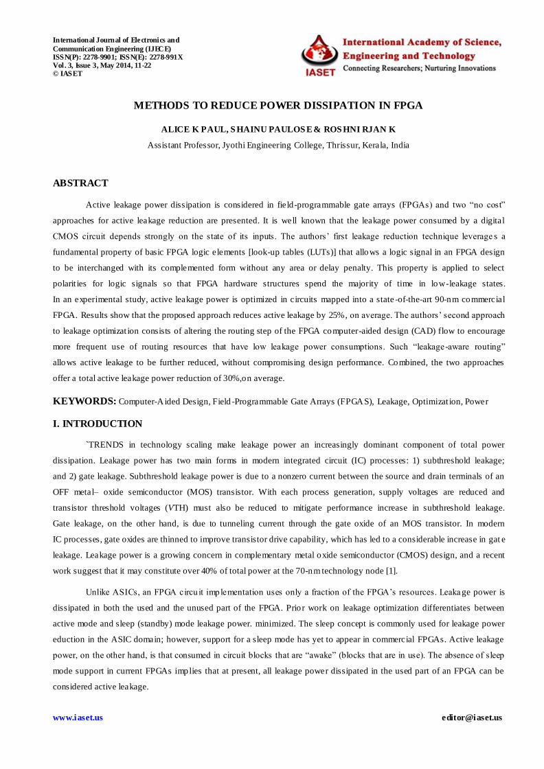
Figure 1: LUT Circuit Implementation; Illustration of Signal Inversion (a) Original Circuit
(b) 2-LUT Implementation (c) After Signal Inversion
II. ACTIVE LEAKAGE POWER OPTIMIZATION VIA INTELLIGENT POLARITY SELECTION
Figure 1 illustrates how a signal’s polarity can be reversed in an FPGA. Figure 1(a) shows a logic circu it having
two AND gates and an exclusive-OR gate. Figure 1(b) of the figure shows the circuit mapped into two-input LUTs.
In this example, the aim is to invert the signal int, so that its complemented rather than its true form is produced by a LUT
and routed through the FPGA interconnection network. There are two steps to inverting a signal. First, the programming of
the LUT producing the signal must be changed. Specifically, to invert the signal, all of the 0s in its driv ing LUT must be
changed to 1s and the 1s must be changed to 0s. Second, the programming of LUTs that are fan outs of the inverted signal
must be altered to “expect” the inverted form. This is achieved by permuting the bits in the SRAM cells of such
“downstream” LUTs. Figure 1(c) shows the circuit after the signal int is inverted. The permutation of bits in the inverted
signal’s fanout LUT is shown through shading: the contents of the top two SRAM cells in the downstream LUT are
interchanged with the contents of the bottom two SRAM cells in the LUT. Through this method, signal inversion in
Methods to Reduce Power Dissipation in FPGA 13
www.iaset.us edi [email protected]
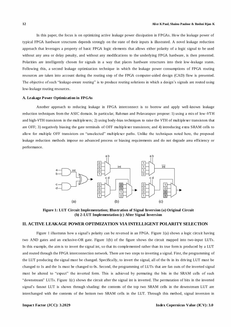
FPGAs can be achieved by simply reprogramming LUTs. The first approach to leakage power optimizat ion is shown in
Figure 2. The input to the algorithm is an FPGA circuit as well as static probability values for each signal in the circuit
Iteration through the signals is carried out and those signals having static pro bability less than 0.5 are selected.
Such signals spend most of their time in the logic 0 state and, thus, they are candidates for inversion. For each candidate
signal, first it must be checked if it can be inverted (discussed below After processing all signals, the output of the
proposed algorithm is a modified design, having signals that spend the majority of their time in the logic state favorable to
low leakage power.
Figure 2: Leakage Optimization Algorithm
Altering the polarity of a signal n with static probability P(n), changes the signal’s probability to 1-P(n).
Therefore, for signals having static probability close to 0.5, the benefits of inversion on leakage optimizat ion are minimal,
since the static probability of such signals remains close to 0.5 after inversion. Low leakage power can be achieved when
signals have static probability close to 0 or 1. The question that arises then is whether the signals in real circu its exhibit th is
property. It is shown below that it is unlikely that the majority of signals in circuits will have probabilities close to 0.5,
which bodes well for the proposed leakage optimizat ion approach.
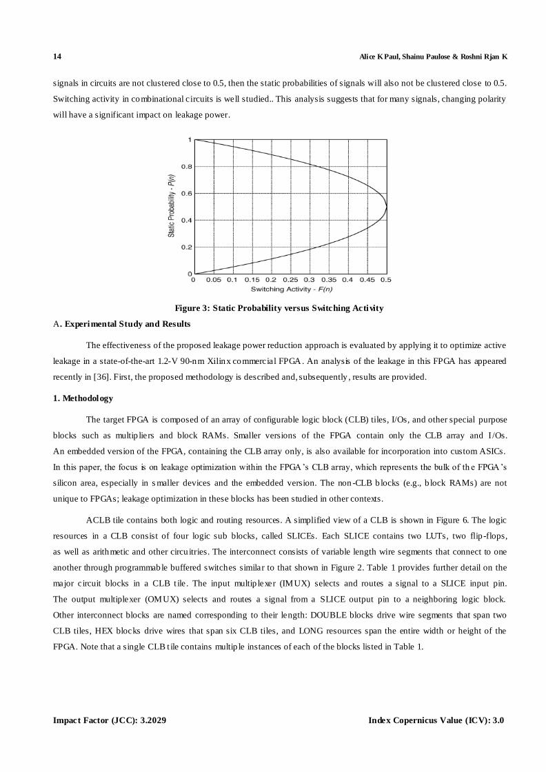
The average rate of logic transitions on a (nonclock) signal n, F(n), can be expressed as a function of the signal’s
static probability .
(1)
Where F(n) is commonly referred to as signal n’s normalized switching activity. F(n) ranges from 0 to 0.5 and can
be interpreted as the fraction of clock cycles in which signal n toggles. Note that (1) is a frequently used approximation that
becomes exact in the absence of temporal correlat ions in signal n’s switching activity (n’s values in two consecutive clock
cycles are independent). Solv ing (1) for P(n) y ields
(2)
Which is plotted in Figure 5. Observe that P(n) is 0.5 only when F(n) is 0.5 and that for a fixed decrease in F(n),
there is a change in P(n) towards either 0 o r 1. From Figure 5, it is inferred that if the switching activ ities of the majority of
14 Alice K Paul, Shainu Paulose & Roshni Rjan K
Impact Factor (JCC): 3.2029 Index Copernicus Value (ICV): 3.0
signals in circuits are not clustered close to 0.5, then the static probabilities of signals will also not be clustered close to 0.5.
Switching activity in combinational circuits is well studied.. This analysis suggests that for many signals, changing polarity
will have a significant impact on leakage power.
Figure 3: Static Probability versus Switching Activity
A. Experimental Study and Results
The effectiveness of the proposed leakage power reduction approach is evaluated by applying it to optimize active
leakage in a state-of-the-art 1.2-V 90-nm Xilinx commercial FPGA. An analysis of the leakage in this FPGA has appeared
recently in [36]. First, the proposed methodology is described and, subsequently , results are provided.
1. Methodology
The target FPGA is composed of an array of configurable logic block (CLB) tiles, I/Os, and other special purpose
blocks such as multip liers and block RAMs. Smaller versions of the FPGA contain only the CLB array and I /Os.
An embedded version of the FPGA, containing the CLB array only, is also available for incorporation into custom ASICs.
In this paper, the focus is on leakage optimization within the FPGA’s CLB array, which represents the bulk of th e FPGA’s
silicon area, especially in s maller devices and the embedded version. The non -CLB b locks (e.g., b lock RAMs) are not
unique to FPGAs; leakage optimization in these blocks has been studied in other contexts.
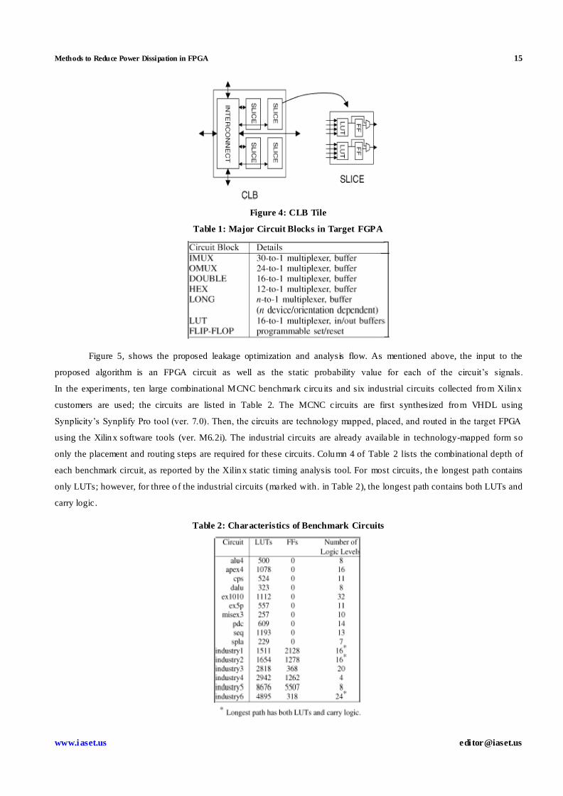
ACLB tile contains both logic and routing resources. A simplified view of a CLB is shown in Figure 6. The logic
resources in a CLB consist of four logic sub blocks, called SLICEs. Each SLICE contains two LUTs, two flip-flops,
as well as arithmetic and other circu itries. The interconnect consists of variable length wire segments that connect to one
another through programmable buffered switches similar to that shown in Figure 2. Table 1 provides further detail on the
major circuit blocks in a CLB t ile. The input multip lexer (IMUX) selects and routes a signal to a SLICE input pin.
The output multiplexer (OMUX) selects and routes a signal from a SLICE output pin to a neighboring logic block.
Other interconnect blocks are named corresponding to their length: DOUBLE blocks drive wire segments that span two
CLB tiles, HEX blocks drive wires that span six CLB tiles, and LONG resources span the entire width or height of the
FPGA. Note that a single CLB t ile contains multip le instances of each of the blocks listed in Table 1.
Methods to Reduce Power Dissipation in FPGA 15
www.iaset.us edi [email protected]
Figure 4: CLB Tile
Table 1: Major Circuit Blocks in Target FGPA
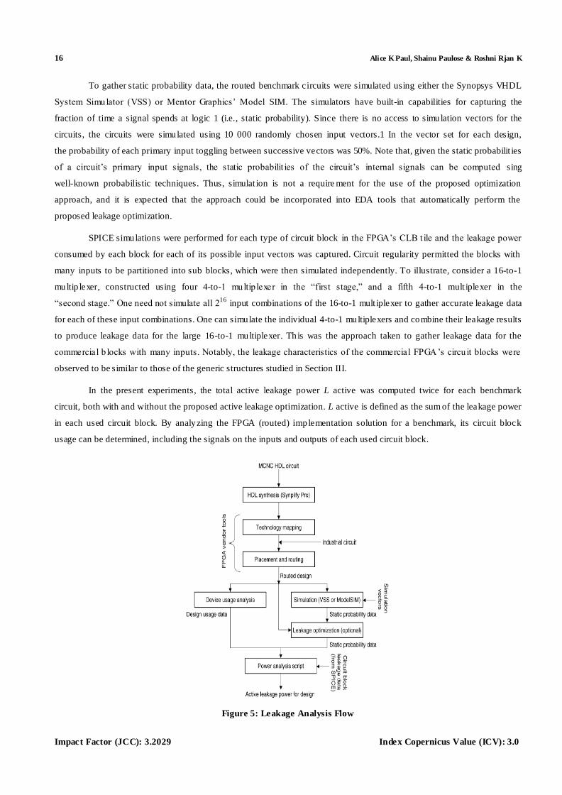
Figure 5, shows the proposed leakage optimization and analysis flow. As mentioned above, the input to the
proposed algorithm is an FPGA circuit as well as the static probability value for each of the circuit’s signals.
In the experiments, ten large combinational MCNC benchmark circu its and six industrial circuits collected from Xilinx
customers are used; the circuits are listed in Table 2. The MCNC circuits are first synthesized from VHDL using
Synplicity’s Synplify Pro tool (ver. 7.0). Then, the circuits are technology mapped, placed, and routed in the target FPGA
using the Xilinx software tools (ver. M6.2i). The industrial circuits are already available in technology-mapped form so
only the placement and routing steps are required for these circuits. Column 4 of Table 2 lists the combinational depth of
each benchmark circuit, as reported by the Xilinx static timing analysis tool. For most circuits, th e longest path contains
only LUTs; however, for three o f the industrial circuits (marked with . in Table 2), the longest path contains both LUTs and
carry logic.
Table 2: Characteristics of Benchmark Circuits
16 Alice K Paul, Shainu Paulose & Roshni Rjan K
Impact Factor (JCC): 3.2029 Index Copernicus Value (ICV): 3.0
To gather static probability data, the routed benchmark circuits were simulated using either the Synopsys VHDL
System Simulator (VSS) or Mentor Graphics’ Model SIM. The simulators have built-in capabilities for capturing the
fraction of time a signal spends at logic 1 (i.e., static probability). Since there is no access to simulation vectors for the
circuits, the circuits were simulated using 10 000 randomly chosen input vectors.1 In the vector set for each design,
the probability of each primary input toggling between successive vectors was 50%. Note that, given the static probabilit ies
of a circuit’s primary input signals, the static probabilit ies of the circuit’s internal signals can be computed sing
well-known probabilistic techniques. Thus, simulat ion is not a require ment for the use of the proposed optimization
approach, and it is expected that the approach could be incorporated into EDA tools that automatically perform the
proposed leakage optimization.
SPICE simulations were performed for each type of circuit block in the FPGA’s CLB t ile and the leakage power
consumed by each block for each of its possible input vectors was captured. Circuit regularity permitted the blocks with
many inputs to be partitioned into sub blocks, which were then simulated independently. To illustrate, consider a 16-to-1
multip lexer, constructed using four 4-to-1 multip lexer in the “first stage,” and a fifth 4-to-1 mult iplexer in the
“second stage.” One need not simulate all 216
input combinations of the 16-to-1 mult iplexer to gather accurate leakage data
for each of these input combinations. One can simulate the individual 4-to-1 multiplexers and combine their leakage results
to produce leakage data for the large 16-to-1 multiplexer. Th is was the approach taken to gather leakage data for the
commercial b locks with many inputs. Notably, the leakage characteristics of the commercial FPGA’s circu it blocks were
observed to be similar to those of the generic structures studied in Section III.
In the present experiments, the total active leakage power L active was computed twice for each benchmark
circuit, both with and without the proposed active leakage optimization. L active is defined as the sum of the leakage power
in each used circuit block. By analyzing the FPGA (routed) implementation solution for a benchmark, its circuit block
usage can be determined, including the signals on the inputs and outputs of each used circuit block.
Figure 5: Leakage Analysis Flow
Methods to Reduce Power Dissipation in FPGA 17
www.iaset.us edi [email protected]
Computing the leakage for a used instance of a circuit b lock in a benchmark involves combining the power data
extracted from the block’s SPICE simulat ion with usage data from the benchmark circu it’s FPGA implementation and
static probability data from the benchmark’s HDL simulation. It is worth reinforcing that the po wer data presented in
Section III are not used; power data extracted from SPICE simulations of the commercial FPGA’s circuit blocks are used
instead.
Consider a used instance B of a circuit block in a benchmark and let represent an input vector that may be
presented to block B. Each bit bi in vector corresponds to an input i on block B. Let SB,i represent the signal on input
i of block B in the benchmark’s FPGA implementation. The static probability of signal SB,i, P(SB,i ), is a known quantity,
extracted from the benchmark’s HDL simulation. If b it bi is logic 1 in vector v , then the static probability of bit bi, PB (bi),
is defined to be equal to P(SB,i). On the other hand, if bi is logic 0 in , then PB(bi) is defined to be 1-P(S B,i)
The probability of vector v appearing on the inputs of block B, PB( ), can be computed as the product of its constituent
bit probabilities
(3)
The average active leakage power for a used circuit block B, Lactive(B), is computed as a weighted sum of the
leakage power consumed by B for each of its input vectors
(4)
Where VB represents the set of all possible input vectors for circuit block B and L active(B ) represents the
leakage power consumed by block B when its input state is vector obtained from SPICE simulations.
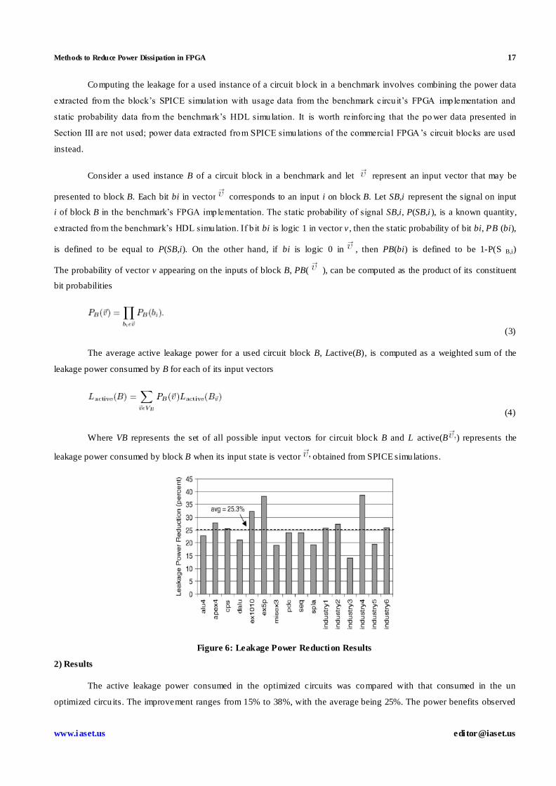
Figure 6: Leakage Power Reduction Results
2) Results
The active leakage power consumed in the optimized circuits was compared with that consumed in the un
optimized circu its. The improvement ranges from 15% to 38%, with the average being 25%. The power benefits observed
18 Alice K Paul, Shainu Paulose & Roshni Rjan K
Impact Factor (JCC): 3.2029 Index Copernicus Value (ICV): 3.0
are quite substantial, considering that the proposed optimizat ion has no impact on circuit area or delay and requires no
hardware changes.
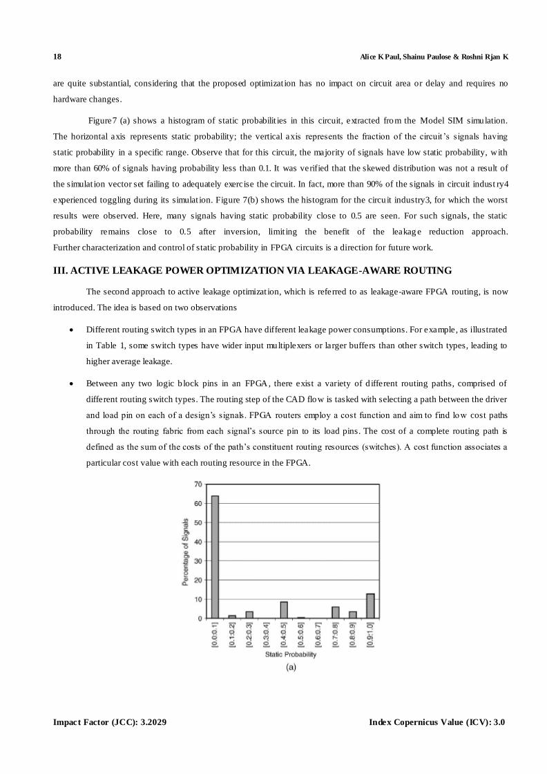
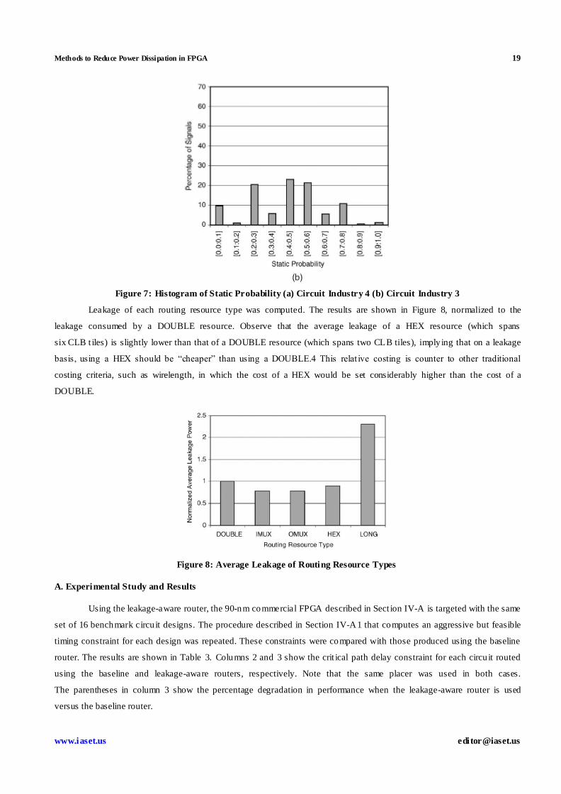
Figure7 (a) shows a histogram of static probabilit ies in this circuit, extracted from the Model SIM simulation.
The horizontal axis represents static probability; the vertical axis represents the fraction of the circuit ’s signals having
static probability in a specific range. Observe that for this circuit, the majority of signals have low static probability, with
more than 60% of signals having probability less than 0.1. It was verified that the skewed distribution was not a result of
the simulat ion vector set failing to adequately exercise the circuit. In fact, more than 90% of the signals in circuit indust ry4
experienced toggling during its simulat ion. Figure 7(b) shows the histogram for the circu it industry3, for which the worst
results were observed. Here, many signals having static probability close to 0.5 are seen. For such signals, the static
probability remains close to 0.5 after inversion, limit ing the benefit of the leakag e reduction approach.
Further characterization and control of static probability in FPGA circuits is a direction for future work.
III. ACTIVE LEAKAGE POWER OPTIMIZATION VIA LEAKAGE-AWARE ROUTING
The second approach to active leakage optimizat ion, which is referred to as leakage-aware FPGA routing, is now
introduced. The idea is based on two observations
Different routing switch types in an FPGA have different leakage power consumptions. For example, as illustrated
in Table 1, some switch types have wider input multiplexers or larger buffers than other switch types, leading to
higher average leakage.
Between any two logic b lock pins in an FPGA, there exist a variety of d ifferent routing paths, comprised of
different routing switch types. The routing step of the CAD flow is tasked with selecting a path between the driver
and load pin on each of a design’s signals. FPGA routers employ a cost function and aim to find low cost paths
through the routing fabric from each signal’s source pin to its load pins. The cost of a complete routing path is
defined as the sum of the costs of the path’s constituent routing resources (switches). A cost function associates a
particular cost value with each routing resource in the FPGA.
Methods to Reduce Power Dissipation in FPGA 19
www.iaset.us edi [email protected]
Figure 7: Histogram of Static Probability (a) Circuit Industry 4 (b) Circuit Industry 3
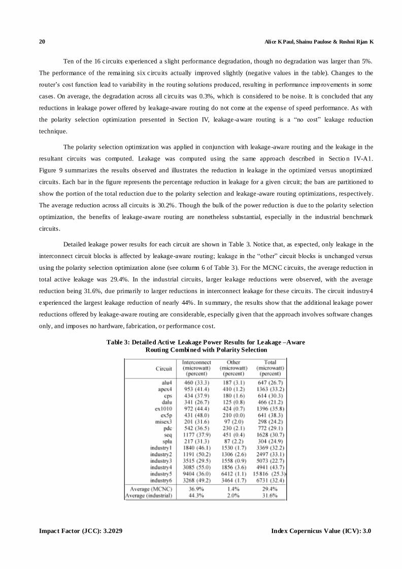
Leakage of each routing resource type was computed. The results are shown in Figure 8, normalized to the
leakage consumed by a DOUBLE resource. Observe that the average leakage of a HEX resource (which spans
six CLB t iles) is slightly lower than that of a DOUBLE resource (which spans two CLB tiles), imply ing that on a leakage
basis, using a HEX should be “cheaper” than using a DOUBLE.4 This relat ive costing is counter to other traditional
costing criteria, such as wirelength, in which the cost of a HEX would be set considerably higher than the cost of a
DOUBLE.
Figure 8: Average Leakage of Routing Resource Types
A. Experimental Study and Results
Using the leakage-aware router, the 90-nm commercial FPGA described in Sect ion IV-A is targeted with the same
set of 16 benchmark circu it designs. The procedure described in Section IV-A1 that computes an aggressive but feasible
timing constraint for each design was repeated. These constraints were compared with those produced using the baseline
router. The results are shown in Table 3. Columns 2 and 3 show the crit ical path delay constraint for each circu it routed
using the baseline and leakage-aware routers, respectively. Note that the same placer was used in both cases.
The parentheses in column 3 show the percentage degradation in performance when the leakage-aware router is used
versus the baseline router.
20 Alice K Paul, Shainu Paulose & Roshni Rjan K
Impact Factor (JCC): 3.2029 Index Copernicus Value (ICV): 3.0
Ten of the 16 circuits experienced a slight performance degradation, though no degradation was larger than 5%.
The performance of the remaining six circu its actually improved slightly (negative values in the table). Changes to the
router’s cost function lead to variability in the routing solutions produced, resulting in performance improvements in some
cases. On average, the degradation across all circu its was 0.3%, which is considered to be noise. It is concluded that any
reductions in leakage power offered by leakage-aware routing do not come at the expense of speed performance. As with
the polarity selection optimization presented in Section IV, leakage-aware routing is a “no cost” leakage reduction
technique.
The polarity selection optimizat ion was applied in conjunction with leakage-aware routing and the leakage in the
resultant circuits was computed. Leakage was computed using the same approach described in Sectio n IV-A1.
Figure 9 summarizes the results observed and illustrates the reduction in leakage in the optimized versus unoptimized
circuits. Each bar in the figure represents the percentage reduction in leakage for a given circuit; the bars are partitioned to
show the portion of the total reduction due to the polarity selection and leakage-aware routing optimizations, respectively.
The average reduction across all circuits is 30.2%. Though the bulk of the power reduction is due to the polarity selection
optimization, the benefits of leakage-aware routing are nonetheless substantial, especially in the industrial benchmark
circuits.
Detailed leakage power results for each circuit are shown in Table 3. Notice that, as expected, only leakage in the
interconnect circuit blocks is affected by leakage-aware routing; leakage in the “other” circuit blocks is unchanged versus
using the polarity selection optimization alone (see column 6 of Table 3). For the MCNC circuits, the average reduction in
total active leakage was 29.4%. In the industrial circuits, larger leakage reductions were observed, with the average
reduction being 31.6%, due primarily to larger reductions in interconnect leakage for these circu its. The circuit industry4
experienced the largest leakage reduction of nearly 44%. In summary, the results show that the additional leakage power
reductions offered by leakage-aware routing are considerable, especially g iven that the approach involves software changes
only, and imposes no hardware, fabrication, o r performance cost.
Table 3: Detailed Active Leakage Power Results for Leakage –Aware
Routing Combined with Polarity Selection

Methods to Reduce Power Dissipation in FPGA 21
www.iaset.us edi [email protected]
Figure 9: Leakage Power Reduction Results for Combined Polarity Selection and Leak age-Aware Routing
The cost of a HEX resource in the leakage-aware router is similar to that of a DOUBLE resource. Whereas, in the
baseline router, the cost of HEX is higher than that of a DOUBLE. Certain ly, leakage-aware routing leads to higher HEX
utilizat ion, and since the capacitance of a HEX is larger than that of a DOUBLE, it is conceivable that leakage aware
routing may increase dynamic power consumption. A future research direction is to investigate this possibility, and, if
deemed a problem, to enhance leakage-aware routing to account for it, perhaps by taking signal switching activity into
account when deciding how a signal should be routed. That being said, it is anticipated that the proposed techniques will be
applied in a future low-leakage FPGA, perhaps implemented in 65- or 45-nm process technology. At such technology
nodes, it is expected that leakage power, not dynamic power, will be the overriding power consideration.
VI. CONCLUSIONS
Trends in technology and voltage scaling have made leakage power a first class cons ideration in digital
complementary metal oxide semiconductor (CMOS) design. In this paper, two “no cost” approaches to active leakage
power reduction in field-programmable gate arrays (FPGAs) were presented. First, the leakage power characteristics of
common FPGA hardware structures were studied. It was observed that the leakage comsumed by FGPA interconnect and
logic circuitry depends strongly on the applied input state. A novel approach for leakage power reduction in which
polarit ies are selected for logic signals to place hardware structures into low-leakage states as much as possible was
proposed.
The proposed technique is based on a unique property of FPGA logic elements [look-up tables (LUTs)] that
permits either the true or complemented form of a signal to be generated, without any area or delay penalty. Experimental
results for a 90-nm state-of the- art commercial FPGA show that the proposed approach reduces active leakage by 25%,
on average. Subsequently, the idea of leakage-aware routing was introduced, in which the cost function used during the
routing step of the FPGA computer aided design (CAD) flow is altered to consider the leakage power consumptions of
routing resources. Leakage-aware routing incurs no significant performance penalty and offers additional leakage
reductions. Combin ing the two techniques produces a total active leakage reduction of up to 44%, with the average
reduction being 30%.
22 Alice K Paul, Shainu Paulose & Roshni Rjan K
Impact Factor (JCC): 3.2029 Index Copernicus Value (ICV): 3.0
REFERENCES
1. J. Kao, S. Narendra, and A. Chandrakasan, “Subthreshold leakage modeling and reduction techniques,” in Proc.
IEEE/ACM Int. Conf. Computer- Aided Design, San Jose, CA, 2002, pp. 141–148.
2. K. Poon, A. Yan, and S. J. E. Wilton, “A flexib le power model for FPGAs,” in Proc. Int. Conf. Field
Programmable Logic and Applications, Montpellier, France, 2002, pp. 312–321.
3. J. Anderson, F. Najm, and T. Tuan, “Active leakage power optimizat ion for FPGAs,” in Proc. ACM/SIGDA Int.
Symp. Field Programmable Gate Arrays, Monterey, CA, 2004, pp. 33–41.
4. Virtex II PRO FPGA Data Sheet. San Jose, CA: Xilinx, Inc., 2003.
5. G. Lemieux and D. Lewis, “Circuit design of routing switches,” in Proc. ACM/SIGDA Int. Symp. Field
Programmable Gate Arrays,Monterey, CA, 2002, pp. 19–28.
6. D. Lewis, V. Betz, D. Jefferson, A. Lee, C. Lane, P. Leventis,S. Marquardt, C. McClintock, B. Ped ersen,
G. Powell, S. Reddy,C. Wysocki, R. Cliff, and J. Rose, “The Stratix routing and logic architecture,” in Proc.
ACM/SIGDA Int. Symp. Field Programmable Gate Arrays, Monterey, CA, 2003, pp. 12–20.
7. A. Rahman and V. Po lavarapuv, “Evaluation of low-leakage design techniques for field-programmable gate
arrays,” in Proc. ACM/SIGDA Int. Symp. Field Programmable Gate Arrays, Monterey, CA, 2004, pp. 23–30.
8. F. Li, Y. Lin, and L. He, “FPGA power reduction using configurable dual-Vdd,” in Proc. ACM/IEEE Design
Automation Conf., San Diego, CA, 2004, pp. 735–740.
9. A. Gayasen, K. Lee, N. Vijaykrishnan, M. Kandemir, M. Irwin, and T. Tuan, “A dual-Vdd low power FPGA
architecture,” in Proc. Int. Conf. Field Programmable Logic and Applications, Antwerp, Belg ium, 2004,
pp. 145–157.
10. L. Ciccarelli, A. Lodi, and R. Canegallo, “Low leakage circuit design for FPGAs,” in Proc. IEEE Custom
Integrated Circuits Conf., Orlando,FL, 2004, pp. 715–718.
11. G. Yeap, Practical Low Power Digital VLSI Design . Boston, MA: Kluwer, 1998.