1982 , volume , issue aug-1982 - hp labsviewpoints 1c process technology: vlsi and beyond by...
TRANSCRIPT
A U G U S T 1 9 8 2
N A L
06301W25KUM0 . 5 U © Copr. 1949-1998 Hewlett-Packard Co.

H E W L E T T - P A C K A R D J O U R N A L Technical In format ion f rom the Laborator ies of Hewlet t -Packard Company
AUGUST 1982 Volume 33 • Number 8
Contents:
Viewpo in t s †” 1C P rocess Techno logy : VLS I and Beyond , by F rede r i c N . Schwe t tmann a n d J o h n L M o l l T h e d e m a n d f o r e v e r - s m a l l e r d e v i c e d i m e n s i o n s r e q u i r e s c o n t i n u a l
advances in 1C fabr icat ion techniques. Here 's where we s tand today.
Op t i ca l 1C L i t hog raphy Us ing T r i l aye r Res i s t , by M ichae l M . O 'Too le , E . Dav id L iu , and Gary caused and Us ing t h ree l aye rs m in im izes exposu re va r i a t i ons caused by bu l k and s tanding-wave ef fects .
S i l i c o n I n t e g r a t e d C i r c u i t s U s i n g B e a m - R e c r y s t a l l i z e d P o l y s i l i c o n , b y T h e o d o r e I . Kamins improves a th in layer of polys i l icon to the mel t ing point and le t t ing i t cool improves
i ts character is t ics for device fabr icat ion.
X - R a y L i t h o g r a p h y , b y G a r r e t t A . G a r r e t t s o n a n d A r m a n d P . N e u k e r m a n s S o f t X - r a y radiat ion shows promise as the next s tep in the evolut ion of VLSI c i rcu i t l i thography.
D ry E t ch ing : An Ove rv i ew , by Pau l J . Ma rcoux Rep lac i ng l i qu i d e t ch ing p rocesses w i t h plasma detect ion. techniques improves control over etch direct ion and endpoint detect ion.
T h i n F i l m s F o r m e d b y P l a s m a - E n h a n c e d C h e m i c a l V a p o r D e p o s i t i o n , b y D r a g a n B . l l i c Lower CVD process tempera tures can be used w i th th is approach.
E l e c t r o m i g r a t i o n : A n O v e r v i e w , b y P a u l P . M e r c h a n t T h i s 1 C c o n d u c t o r f a i l u r e mechanism can be a l imi t ing factor to shr ink ing VLSI c i rcu i t d imensions.
SWAMI: process Zero-Encroachment Local Oxidat ion Process, byKuang YiChiu This process minimizes lateral oxidat ion which al ters cr i t ical device dimensions and l imits c i rcui t densi ty.
H igh -P ressu re Ox ida t i on , by W i l l i am A . B rown I nc reas ing t he p ressu re o f t he ox i d i z i ng gas reduces the t ime and temperature requ i red for a s i l i con ox idat ion cyc le .
In this Issue:
The appl icat ion of s i l icon in tegrated c i rcu i ts has become pervasive in a lmost a l l human act ivi t ies. I t is expected that this pervasiveness wi l l continue to expand at least through the end of of century, characterized by higher and higher levels of integration — more and more t ransis tors in the same s i l icon area. We are enter ing the era of VLSI — very large-scale integration — which means hundreds of thousands of devices on a single chip of sil icon. One of the key driving forces behind this trend is the rapid, exhilarating development of the process technologies required for fabr icat ing VLSI c i rcui ts . Remarkable advances have been ¡m-
üSi plemented in manufactur ing that were bel ieved to be impossible a few short years ago. In this Hewlett-Packard a number of the process technologies currently being explored at Hewlett-Packard are de
scribed. The strong interdiscipl inary nature of these evolving technologies is readi ly apparent and wil l be more extensive in the future. With cri t ical dimensions in some cases approaching several atomic layers, the intr icacy of these processes is increasing and we will in the next 5 to 10 years begin to see the limits of some technologies defined and perhaps approached. Unti l then, the cramming of more features on a chip to get higher performance wi th less power d iss ipat ion wi l l cont inue at a rapid pace.
C o v e r : E d i t o r s o l a r i z e d v e r s i o n o f F i g . 8 , p a g e 8 . - F r e d e r i c N . S c h w e t t m a n n , G u e s t E d i t o r
E d i t o r . R i c h a r d P D o l a n â € ¢ A s s o c i a t e E d i t o r K e n n e t h A S h a w . A r t D i r e c t o r , P h o t o g r a p h e r . A r v i d A D a n i e l s o n â € ¢ I l l u s t r a t o r . N a n c y S V a n d e r b l o o m A d m i n i s t r a t i v e S e r v i c e s T y p o g r a p h y . A n n e S . L o P r e s t i . S u s a n E W r i g h t â € ¢ E u r o p e a n P r o d u c t i o n S u p e r v i s o r , H e n k V a n L a m m e r e n
2 H E W L E T T - P A C K A R D J O U R N A L A U G U S T 1 9 8 2 Â © H e w l e t t - P a c k a r d C o m p a n y 1 9 8 2 P r i n t e d i n U . S . A .
© Copr. 1949-1998 Hewlett-Packard Co.

Viewpoints
1C Process Technology: VLSI and Beyond by Freder ic N. Schwettmann and John L. Mol l
THE VLSI ERA is here. Integrated circuits containing over 100.000 devices with l-to-2-micrometer feature sizes have become a manufacturing reality. A prime example of the
power of this technology is the demonstration of a 450.000-device, 32-bit microcomputer operating at a clock rate of 18 MHz.1 This remarkable accomplishment is the result of the congruence of advances in design automation, process technology, packaging and testing. In the field of process technology, significant achievements have been demonstrated in lithography, etching, interconnections, materials and low-temperature processing. Now that VLSI has become a reality, where and how far the technology can be extended are key questions facing researchers the world over. Device Scaling
The presently available processing capability of defining dimen sions as small as 1 to 1.5 micrometers will be driven down to even smaller sizes. The general device performance guideline of constant-field scaling has been followed as metal-oxide- semiconductor (MOS) device dimensions are reduced, but with significant violations. The average voltage drop per micrometer along the device channel has increased somewhat, and the maximum electric field in the gate dielectric has increased. In addition, the channel length has decreased faster than the junction depths time the source and drain regions. The result is that from time to time new physical phenomena need to be included in describing device operation and electrical characteristics, and in determining the sensitivity of circuit operation to process variations.
Up to this time, scaling of both lateral and vertical dimensions has been advantageous, both to functional integration and to cir cuit performance. As the dimensions become less than one mi crometer the performance advantage will become more difficult to maintain. Parasitic resistance will increase, and as chips become more to parasitic capacitance will be more difficult to con- frol. and lower operating voltage tends to reduce noise margin and places greater demands on process control. There is in fact a proba bility that at some minimal dimension, performance will peak, limited by parasitic effects and unscalable parameters such as operating temperature and subthreshold conduction.
An often asked question is "What are the minimum usable line and space sizes for silicon VLSI?" A proposed answer for the minimum feature, both in an MOS device and in interconnect lines, is approximately 0.25 micrometer. Thermodynamic and quantum-mechanical effects begin to limit device and circuit per formance at sufficiently small dimensions. There are more pragmat ic considerations, such as the previously mentioned parasitic ef fect on performance, and limitations in the perfection and control of fabrication processes. The cost of building and maintaining a facility to achieve the necessary degree of control for submicrome- ter VLSI will certainly far exceed present-day factory costs.
There are still a number of "aces in the hole" that make the ultimate scaling and performance of silicon VLSI a moving target. The discussion to this point has centered around MOS switches built possi the self-aligned silicon gate configuration. There are possi ble process inventions that could, for example, significantly reduce the parasitic and interconnect limits (see article on page 3 1 and box on page 33). Device inventions such as multilevel films of active
•Constant-field scaling means that if, when the physical dimensions of a device are reduced, the operat ing vol tages and currents are a lso reduced so that the e lect r ic f ie lds wi th in the d e v i c e i s c o n s t a n t , p e r f o r m a n c e s h o u l d r e m a i n t h e s a m e . I n p r a c t i c e t h i s i s d i f f i c u l t to do because o f the need for a s tandard operat ing vo l tage.
devices could also affect system architecture. There is so much activity in both new processes and new device configurations that any attempt to report all of the efforts would fall far short of the mark.
Lithography The dominant lithographic technology currently used in 1C
manufacturing is the 1:1 optical projection printer. This tool allows geometries as small as two micrometers and affords high wafer throughput. Below two micrometers, the trend has been to step- and-repeat exposure systems. In addition to better resolution, these tools provide greater alignment accuracy. As a general guideline, the layer-to-layer registration is targeted to be no worse than 0.25 times a minimum resolvable feature size. Therefore, for a 1-jum technology, the layer-to-layer registration should be better than ±0.25 /urn, a value well within the capability of a state-of-the-art step-and-repeat system. It is expected that as the numerical aper ture of the lenses used in the optical system is increased and the wavelength of the exposing light is decreased, a real limit of 0.5 /¿m for refractive optics will be approached. Crucial to the success of optical systems in the submicrometer regime is the use of a mul tilayer resist technology (see article on page 5). Much effort is being expended in this area to extend the usable range of optical systems. Higher may resists such as those using inorganic materials may ultimately replace the organic photoresists now in common use.
At 0.5 micrometer and smaller, X-ray and electron beam lithog raphy are the contenders. Electron beam has demonstrated fine- line capability and possesses excellent alignment potential. How ever, the is currently lower than for optical systems and the cost is considerably higher. X-ray, on the other hand, has excellent resolution capability and the potential for higher throughput (see article on page 14). For dimensions less than 0.5 micrometer, step- and-repeat systems would be required to achieve the desired over lay accuracy. This eases the mask fabrication problems, but re quires that a more intense source of X-rays be used and/or a more sensitive resist developed. Clearly, much technological progress is required.
Etching Once a pattern has been defined in the resist, it must be faithfully
reproduced in the underlying layer. Before the advent of VLSI, etching was usually done with wet chemistry. This technology almost always has the virtue of nearly infinite selectivity (ability to etch iso- material without affecting another material), but is iso- tropic. For geometries greater than two micrometers, this is not a significant problem. However, when etching a 1-jum-wide pattern in a layer that is 0.5-/xm thick, the lateral portion of isotropic etching completely destroys the pattern. For most VLSI applica tions and all future submicrometer work, anisotropic etching will be essential. The use of dry plasma processes has emerged as the primary etch technology (see article on page 19).
The transition from wet to dry etching has been difficult. The required equipment (see box on page 22) is more complex, more expensive and has lower wafer throughput when compared to wet etching. In addition to anisotropy and good selectivity, sloped sidewalls are required to provide conformal step coverage for sub sequent layers. The task is to find the right combination of gases and process conditions to match the requirements. An enduring significant problem is the lack of understanding of the mechanisms associated with anisotropy, etch rate and selectivity. Much work is
AUGUST 1982 HEWLETT-PACKARD JOURNAL 3
© Copr. 1949-1998 Hewlett-Packard Co.
required in this area.
Interconnections As the speed of individual devices increases, the time delays
associated with the interconnections begins to play a significant role in circuit performance. As the minimum feature size is de creased, the area of the interconnect and the contact area become smaller. The time delay is dependent on the resistance of the interconnections and the capacitance controlled primarily by the dielectric layer. The dielectric material in most cases is either silicon dioxide or silicon nitride.
For the device interconnections, a variety of materials are availa ble. Refractory metal suicides on top of polysilicon are gradually replacing polysilicon as a first-level interconnect material. An order-of-magnitude decrease in resistivity is gained by this ap proach. More emphasis is now being placed on two levels of metal lization on top of the polysilicon or polycide layer. This provides greater flexibility for the circuit designer, but adds to the manufac turing difficulty. Three or more levels of metallization are expected to become more common as experience is gained. Aluminum alloy metallization is currently used in almost all VLSI applications. As contacts to diffused areas with shallower junctions are required, barrier layers such as tungsten will be added to prevent spiking through the junctions. To decrease the contact resistance (contact area decreases, and hence resistance increases as the square of the scaling factor), suicide layers such as platinum suicide may be required.
An additional factor, electromigration (see article on page 28), becomes important for circuit reliability as the conductor cross- sectional area decreases and current density increases. This re quirement may result in the replacement of aluminum alloys with materials such as tungsten. However, the higher resistivity of tungsten, about four times higher, results in another tradeoff be tween performance and reliability.
Materials Another area expected to be of great concern in the submicro-
meter region is the silicon material itself. Already great care is being given The tighter control on the specifications of substrates. The amount, distribution and chemical bonding of silicon impurities such their oxygen and carbon are being carefully monitored and their effect on device performance evaluated. The coupling of these species to the defects generated during processing is a major con cern. A variety of gettering schemes are being studied and im plemented where needed. The tools for characterizing defects on a near-atomic level, such as scanning transmission electron micro scopy on are now available and are being brought to bear on the problems with remarkable results. There is much optimism on being able to understand and control the location of defects in silicon.
One novel approach to forming a substrate, discussed in the article on page 10, is the use of an intense laser or electron beam to melt a into layer and then let it cool and recrystallize into large-grain polysilicon suitable for device fabrication.
Low-Temperature Processing The requirements of shallow junctions in scaling and the need
for the minimum lateral motion of dopants requires that processing temperatures be kept as low as possible. Instead of applying energy to deposition and growth processes by thermal means alone, plasma excitation will be used (see article on page 24). Already, deposition of silicon dioxide and silicon nitride by plasma techniques is available for manufacturing processes. Films depos ited using plasma excitation tend to exhibit better step coverage than in thermally deposited films. Interest is now high in
' Enhanced d i f f us ion o f t he con tac t me ta l i n a l oca l i zed a rea o f t he under l y ing semicon ductor junct ion. resul t ing in an e lectr ica l shor t across a device junct ion.
being able to deposit conducting materials such as aluminum and tungsten using plasma techniques.
The growth of thin films in a plasma as opposed to deposition is a new and ni- area. Gate dielectrics of silicon nitride and ni- trided silicon dioxide show promise for scaled devices requiring dielectric layers less than 10 nm thick (see box on page 26). They exhibit better physical durability, lower etch rates and lower defect densities. Much work needs to be done to understand the growth mechanisms and implement these films in the manufacturing environment.
Another approach that will be useful in lowering processing temperatures is high-pressure oxidation (see article on page 34). This could be a useful tool in the submicrometer regime.
In summary, while design tools are still lagging the available process technology, the march toward smaller devices and circuits continues at a furious pace. It is expected that by the turn of the century, the ultimate limits in silicon will have been clearly dem onstrated and maybe attained. Many challenges remain and oppor tunity en for contribution and innovations in almost all en gineering disciplines in reaching this goal.
Reference 1. ). Vol. et al, "A 32b VLSI Chip," Digest of Technical Papers, Vol. 24, IEEE Inter national Solid-State Circuits Conference. February 1981. THAM 9.1.
Freder ic N. Schwettmann Frecl Schwettmann is the director of HP's In- tegrated Circuit Laboratory. His work has re-
j ( su i ted in over 20 publ icat ions and presenta- t ions re la ted to lc techno logy, and three
i patents , two on semiconductor technology, B B M S ' ^ e o t n e r o n P e t r o c h e m i c a l p r o c e s s i n g . H e
â € ¢ à œ à œ I , A & ^ E I J  ° i n e d H P i n 1 9 7 6 w i t h s e v e r a l y e a r s o f e x - > per ience in semiconductor and petrochemi- | calR&D. Fred isthe national vice chairman of I new technologies for the Electrochemical
Soc ie ty and a member o f the VLSI program committee of the IEEE. He was born in Brook lyn , New York and s tud ied chemica l en-
•" | g inee r ing a t t he C i t y Co l l ege o f New York , earn ing a BS degree in 1961, a t New York
University, earning an MS degree in 1964, and at City University of New York, earning a PhD degree in 1969. Fred is marr ied, has two chi ldren, and l ives in San Jose, Cal i fornia. He enjoys running, playing racquetbal l and basketbal l , and sports in general. During his col lege days, Fred was voted "Al l -American" in lacrosse and was se lected as most-va luable p layer for two years.
John L. Mol l John Mol l has been with HP since 1974, f i rst as the di rector of technology for the 1C lab, and most recently as the manager of the ICSR lab and a sen ior sc ien t is t w i th HP Labora tor ies. He is wel l -known to c i rcui t designers for the Ebers-Mol l model of the large-s ignal behavior of t ransistors, has been on the fac ulty of Stanford University, and has extensive exper ience research ing so l id-s ta te dev ices and the phys ics o f so l ids . John 's con t r ibu t ions have resul ted in over 100 papers, ten patents, and a book, Physics of Semiconduc t o rs He was a Guggenhe im Fe l low in 1964 and received the Howard N. Potts award from the Frankl in Inst i tute in 1967 and the Ebers
He is a Fel low of the IEEE and a member of the award from the IEEE in 1971 Amer ican Physical Society, Nat ional Academy of Engineer ing, and Sigma Xi .
4 HEWLETT-PACKARD JOURNAL AUGUST 1982
© Copr. 1949-1998 Hewlett-Packard Co.

Optical 1C Lithography Using Tri layer Resist A composi te photores is t layer reduces exposure e f fec ts that degrade pat tern def in i t ion and reduce resolut ion in opt ical 1C l i thography.
by Michael M, O'Toole , E . David L iu , and Gary W. Ray
THE DENSITY AND PERFORMANCE of devices con tained in today's VLSI circuits are primarily deter mined by the resolution capability of the litho
graphic technique used for the circuits' manufacture. The dominant technology uses an optical projection system to form an image of the desired pattern on the photoresist- covered surface of a silicon wafer. The theoretical image resolution limit of the lens systems in modern projection aligners is in the submicrometer range. However, the reso lution obtainable in normal 1C production is much poorer because of various resist and substrate surface effects.
To achieve dimensional control closer to the theoretical resolution limit of the projection system, a trilayer resist process has been developed. Before describing this process, it is useful to discuss the effects that degrade image resolu tion in conventional processing.
In an ideal situation, the image projected on a planar, nonreflective surface covered with positive resist will con sist of perfectly dark lines, corresponding to the desired features, surrounded by evenly illuminated areas where the resist is exposed and later developed away. In typical 1C fabrication, however, the image is projected onto a nonpla- nar reflective surface that is unevenly covered with resist. The nonplanar reflective surface provides the conditions for two effects that limit the usable resolution of a projection aligner. The bulk effect is caused by large thickness varia tions of the resist near abrupt changes (steps) in the surface topography. The standing-wave effect is caused by multiple reflections of the exposure illumination from the substrate surface.1
The bulk variation in the resist thickness as it covers a step is shown in Fig. I. The resist layer on top of the step is thinner than it is next to the step and, in general, requires less exposure to be developed to the desired linewidth. As a result of the standing-wave effect, variations in the thickness of the resist or any thin semitransparent layers under the resist can cause large variations in the exposure energy coupled into the resist. This effect is periodic within the thickness of a layer. The period is A72n, where A. is the wavelength of the illumination and n is the index of re fraction of the layer material. Even a small thickness varia tion of 0.65 micrometer can cause a major exposure variation. Both effects are most evident for resist feature dimensions
'Some of the data presented in th is ar t ic le has been prev ious ly d iscussed by the authors at the 1981 Symposium on VLSI Technology in Maui, Hawaii and in art ic les publ ished in the November , 1981 issue o f the IEEE Transact ions on E lec t ron Dev ices and the May, 1982 issue of Sol id State Technology
approaching the resolution limit of the projection lens. The standing-wave and bulk effects may be studied by
using a computer program for the simulation of optical projection printing.2 The program assumes diffraction- limited optics, considers the numerical aperture of the im aging lens, the imaging wavelength, the partial coherence factor of the illumination system, and the focus error, and calculates the image intensity pattern for a specified feature on the surface of the resist. The exposure and development of the resist are calculated by using the model described by Dill, et al.3 This model considers the substrate's topography and the characteristics and thickness of the resist. The final output is a simulated line edge profile in positive resist.
A sample output of the simulation program is given in Fig. 2, which shows the nominal exposure required for a periodic l-/um-wide line-and-space pattern as a function of positive resist thickness on (a) a silicon substrate, and (b) an aluminum substrate. The nominal dose is defined as the exposure energy density required to replicate the mask linewidth in the resist. The bulk effect causes the gradual rise of the curve, and the standing-wave effect causes the periodic variation. The period X/2n is 128 nm for an expo sure wavelength of 436 nm and a resist refractive index of 1.69. To compensate the standing-wave effect caused by a 64-nm thickness variation in a l-/um-thick layer of positive resist on a silicon substrate, a 25% exposure difference is required. A similar exposure difference is required to cor-
Fig. 1. Res/si sfep coverage: 1-/¿m-thick resist pattern over 0 .5-nm-high s tep.
AUGUST 1982 HEWLETT-PACKARD JOURNAL 5
© Copr. 1949-1998 Hewlett-Packard Co.

100
E . o
1 5 0
o Q
Patterned Posit ive-Resist Top Layer
(b)
0 . 5 1.0 Resist Thickness (¿t
1.5
F i g . 2 . T h e e x p o s u r e e n e r g y d e n s i t y ( d o s e ) r e q u i r e d a t a wavelength of 436 nm to achieve 1-f jun-wide l ines and spaces in HPFt 204 pos i t i ve res is t on (a ) s i / i con and (b ) a luminum surfaces for numerical aperture N A =0.28, perfect focus, and par t ia l coherence factor <r=0.7.
rect for the bulk effect caused by a 250-nm resist thickness variation. From curve b of Fig. 2, a bulk thickness variation of about 420 nm is equal to a standing-wave thickness variation of 64 nm. Both effects can combine near a step to produce a significant variation in the nominal exposure dose required, causing severe linewidth control problems. Fig. 3 shows a microphotograph of l-/am-wide lines and spaces patterned in a l-/u.m-thick layer of positive resist over two 0.5-/am-high polysilicon lines. The resist linewidth is very unstable near the edge of the steps and narrower on top of the polysilicon lines than in the lower field areas around them.
Intermediate Layer (SiO2,Si3N4 or SOG)
Bottom Layer Polymer (Dye Added)
F ig . 3 . 1 - / j sn -w ide l i nes and spaces in 7 / j / n o f res i s t ove r 0 .5- iun-h igh po lys i l icon s teps.
Substrate
Fig. 4. Tr i layer resist system.
Tri layer Resist Process To realize the maximum resolution from a projection
aligner, the surface of a wafer must behave as if it were planar and nonreflecting. In an attempt to achieve this condition, several multilayer resist processes have been recently proposed and demonstrated.4"9 In a multilayer sys tem, the substrate's topography is planarized by a thick bottom polymer layer. Optical reflections from the underly ing surface topography can be eliminated by choosing an absorptive material for the bottom layer.
Fig. 4 illustrates the trilayer structure studied by Hewlett-Packard Laboratories. An absorbing polymer, one to three micrometers thick, is used to planarize the substrate topography. The planarized surface can be coated uniformly by the top resist layer, thus suppressing the bulk effect. The absorption of the exposure illumination by the bottom polymer layer eliminates reflections from the substrate to pography and reduces the standing-wave effect. An inter mediate inorganic layer serves as a mask during reactive- ion-etching to transfer the top resist layer pattern to the bottom layer. The intermediate layer also prevents mixing of the top and bottom layer polymers.
Suitable materials for the bottom layer are polymers that planarize well. Transparent polymers may be made absorb ing by adding dye. The dye must dissolve in the polymer and absorb strongly at the exposure wavelength. To simplify processing, the dye should be transparent at the alignment wavelength, allowing easy detection of the alignment mark through the thick bottom polymer layer.
Several materials have been used for the intermediate layer. Plasma-enhanced chemical-vapor deposition (PECVD) of silicon nitride done at room temperature is suitable (see article on page 24). Spin-on glass (SOG) has also been used as a suitable intermediate layer.10 Because SOG can be applied by 1C production equipment very simi lar to that used to apply resist, the use of SOG for the intermediate layer makes it easier to incorporate the trilayer process into an 1C production facility. Both PECVD nitride and SOG permit rework of the top resist layer without having to strip the intermediate and bottom polymer layers.
Pattern transfer from the top resist layer to the inter-
6 H E W L E T T - P A C K A R D J O U R N A L A U G U S T 1 9 8 2
© Copr. 1949-1998 Hewlett-Packard Co.
mediate layer is achieved by plasma etching. If SOG is used for the intermediate layer, a CHFs CCb gas mixture is used. The SOG pattern is transferred to the bottom polymer layer using an anisotropic oxygen plasma etch process.
The trilayer process was analyzed and optimized using simulations generated by the computer program mentioned earlier. Positive resist was used for the top and bottom layers and was developed using a conventional batch pro cess. The exposure and development parameters for the positive resist were measured at Hewlett-Packard Laboratories11 using equipment similar to Dill's for the ex posure parameters and to Meyerhofer's12 for the develop ment parameters.
In addition to the optical parameters of the aligner and the exposure and development parameters of the resist, the computer simulation of the trilayer system considers the refractive indexes of the materials and thicknesses of the various layers. Fig. 5 shows the calculated nominal dose required to print l-/xm-wide lines and spaces as a function of the thickness of the bottom polymer for the trilayer sys tem of Fig. 4 on an aluminum substrate. Curve a assumes the absorption of HPR 204 positive resist and curve b assumes the absorption of this resist with dye added.
If the bottom polymer layer does not sufficiently planarize the substrate surface, the top layer of resist will disperse nonuniformly. Curves a and b of Fig. 6 show the calculated linewidth as a function of top resist thickness for two bottom polymer thicknesses of 1.03 /urn and 0.95 /u.m. These two thicknesses represent the two extremes near 1 /j.m of curve a in Fig. 5. In both cases, the simulated expo sure dose has been adjusted to produce a 1 -/urn- wide line for a 0.5-/¿m-thick top resist layer. Both the bulk and standing-wave effects are clearly seen. If the top resist layer is uniformly 0.5-fj.m thick, the nominal exposure required to maintain a one-micrometer dimension changes from 16 mj/cm2 for a 0.95-/u.m-thick bottom layer to 25 mj/cm2 for a 1.03-/u.m-thick bottom layer. This exposure variation is too great to achieve sufficient linewidth control over the entire wafer surface.
Adding dye to the bottom polymer of the trilayer process suppresses the standing-wave effect. Curve c of Fig. 6 shows the linewidth variation versus top resist layer thick ness for a l-/¿m-thick bottom resist layer with dye added. The linewidth variation is caused entirely by the bulk ef-
30 T
2.0-r
20
10 0 . 5
r - 1 . 0 1 . 5 2 . 0
Bottom Layer Polymer Thickness 2.5
Fig. 5. Nominal dose versus bottom polymer thickness for the t r i layer system of F ig . 4 on an a luminum substrate us ing (a) HPR 204 posit ive resist and (b) HPR 204 containing 1.5% dye for the bot tom polymer. Simulat ions are for 1- urn-wide l ines and spaces under per fec t focus cond i t ions .
0 . 3 0 . 4 0 . 5 0 . 6 T o p L a y e r R e s i s t T h i c k n e s s ( f i m )
Fig. 6. Simulated l inewidth versus top res is t layer th ickness for 1-/j im-wide lines and spaces for (a) a 0.95-/jun-thick bottom layer of HPR 204 posi t ive res ist and an exposure dose of 16 mj/cm2 for the top layer of resist , (b) A 1.03-f im-thick bot tom layer of HPR 204 and a 21-mJ!cm2 dose for the top layer, (c) W h e n d y e i s a d d e d t o a 1 . 0 - f i m - t h i c k b o t t o m l a y e r , t h e standing-wave effect on the l inewidth in the top resist layer is el iminated.
feet. Because positive resist used for the bottom polymer has been shown to planarize well,13 the top resist thickness can be held to close tolerance, and good linewidth control is expected.
Experimental Results A resolution test mask was used to print lines and spaces
over topography using the trilayer system and a direct-
minin
F i g . 7 . 1 - n m - w i d e l i n e s a n d s p a c e s i n t r i l a y e r r e s i s t o v e r 0.5-f jun-high aluminum steps af ter react ive ion etch. 2.0-fun- thick HPR 204 posit ive resist containing 1 .5% dye is used for the bot tom polymer layer .
AUGUST 1982 HEWLETT-PACKARD JOURNAL 7
© Copr. 1949-1998 Hewlett-Packard Co.
step-on-wafer (DSW) 10:1 optical projection aligner with a numerical aperture of 0.28 and an imaging wavelength of 436 nm. Fig. 7 shows a scanning-electron-microscope (SEM) microphotograph of l-/um-wide lines and spaces pat terned with a trilayer process over 0.5-/nm aluminized to pography. Because the 2.0-ju.m-thick bottom resist layer planarizes the topography well, the thickness of the top resist layer is controlled to about ±0.03 fjan. The bulk effect is minimized and the standing-wave effect is eliminated. Because the wafer surface appears planar and nonreflective, excellent linewidth control of 1-pim-wide features over 0.5-/xm-high steps is achieved.
Fig. 8 shows the straight sidewalls that are possible with this process. The bottom and intermediate layers in Fig. 8 were etched in a single pumpdown using a reactive-ion- etch system.
Future of Opt ical L i thography Optical lithographic technology continues to evolve,
both in equipment and in resist materials and techniques. Projection aligners with large numerical apertures, shorter imaging wavelengths, and better alignment capability are being designed. Future aligners14 should have a theoreti cal resolution limit well into the submicrometer range and use sophisticated site-by-site autoalignment systems. In addition, new materials such as the inorganic resists6'7'15 may be us ed in a multilayer resist system to further enhance the practical resolution of optical lithography.
100 -r
Fig. for Edge prof i le of tr i layer process using spin-on glass for the intermediate layer cover ing 1 .0-nm-high aluminum steps. Prof i le is shown af ter react ive ion etch ing of bot tom polymer layer.
o o
1 . 0 1 . 5 Linewidth (/¿m)
Fig. 9. The nominal exposure dose as a funct ion of l inewidth in micrometers for (a) A. =436 nm, AM =0.28; (b) X= 405 nm, NA =0.35: and (c) = 240 nm, AM =0.25 («7=0.7, a l l cases) . S i m u l a t i o n p a r a m e t e r s ( s e e r e f e r e n c e 1 1 ) : A = 0 . 5 7 f i m ~ ' , S = 0 . 0 8 j u / n ~ ' , C = 0 . 0 7 c m 2 / m j , F 1 = 0 . 1 7 9 , F 2 = - 0 . 3 4 6 , F 3=0.1 68.
In an ideal multilayer resist system, one where planariza- tion is complete and substrate reflections are completely suppressed, the limits of optical lithography can be explored through computer simulation. The nominal expo sure dose as a function of linewidth under perfect focus conditions for three combinations of numerical aperture and exposure wavelength is shown in Fig. 9. Curves a and b use parameters that roughly correspond to existing projec tion equipment. Curve c simulates a ficticious projection aligner that has an imaging lens with a numerical aperture of 0.25 and an imaging wavelength of 240 nm. The sudden rise in exposure dose for the smaller linewidths indicates a regime where 1C process latitude degrades sharply. Opera tion in the crook of this regime is possible if a set of line- width compensation rules for the larger linewidths is used.
A more explicit view of process latitude is given by Fig. 10 and Fig. 11, which give the fractional linewidth varia tion as a function of linewidth for a ±5% and a ±10% variation in exposure energy. Curves a, b, and c in Fig. 10 and Fig. 11 correspond to curves a, b, and c in Fig. 9. The calculated nominal dose for each linewidth in Fig. 9 was used to generate Fig. 10 and Fig. 11. The curves in Fig. 10 and 11 were calculated assuming a focus error equal to one-half of a "depth of field."
Current optical systems in conjunction with multilayer processing can probably achieve an effective exposure sta bility in this range. From curve b in both Fig . 1 0 and Fig . 1 1 ,
J -1
1 . 0 1 . 5
Linewidth (
Fig. 10. The fract ional l inewidth variat ion (AL/LJ as a function of l inewidth in micrometers for a ±5% var iat ion in exposure e n e r g y f o r t h e c u r v e s o f F i g . 9 . E a c h o p t i c a l s y s t e m w a s degraded by K l [4 (NA)2 ] o f focus e r ro r .
8 H E W L E T T - P A C K A R D J O U R N A L A U G U S T 1 9 8 2
© Copr. 1949-1998 Hewlett-Packard Co.

0.50 —
0 . 2 5 - -
(a)
(b)
(c)
F ig . 11 . The f rac t i ona l l i new id th va r i a t i on as a f unc t i on o f l i new id th fo r a ±10% var ia t ion in exposure energy fo r the curves of Fig. 9.
a projection aligner with a numerical aperture of 0.35 and an imaging wavelength of 405 nm should be able to print a 0.8-fj.m linewidth with 8% to 12% variation in size, using current microfabrication processes. Such an imaging sys tem is commercially available today. As the imaging and alignment systems of optical lithographic equipment im prove during the 1980s, production of VLSI circuits with submicrometer design rules should become a reality.
References 1. J.D. Cuthbert, Solid State Technology, Vol. 20, August 1977, p. 59. 2. W.G. Oldham, et al, IEEE Transactions on Electron Devices, Vol. ED-26, 1979, p. 717. 3. F.J. Dill, et al, IEEE Transactions on Electron Devices, Vol. ED-22, 1975, p. 445. 4. J.M. Moran and D.M. Maydan, Journal of Vacuum Science and Technology, Vol. 16, 1979, p. 1620. 5. J .H. Bruning, Journal of Vacuum Science and Technology, Vol.17, 1980, p. 1147. 6. K.L. Tai, et al, Journal of Vacuum Science and Technology, Vol. 17, 1980, p. 1169. 7. K.L. Tai, et al, Journal of Vacuum Science and Technology Vol. 16, 1979, p. 1977. 8. B.J. Lin, Journal of the Electrochemical Society, Vol. 127, 1980, p. 202. 9. B. Carlson and J. Arnold, presented at the Kodak Microelec tronics Seminar, San Diego, California, October 1980. 10. G.W. Ray, et al, "Spin-On Glass as an Intermediate Layer in a Tri-Layer Resist Process," Accelerated Brief Communications, Journal of the Electrochemical Society, Vol. 129, September 1982. 11. M.M. O'Toole and W.J. Grande, IEEE Electron Device Letters, Vol. EDL-2, December 1981, p. 311. 12. D. Meyerhofer, IEEE Transactions on Electron Devices, Vol. ED-27, 1980, p. 921. 13. M.M. O'Toole, E.D. Liu, and M.S. Chang, presented at SPIE Semiconductor Microlithography VI, San Jose, California, March 1981. 14 . J .Wi lcynski , "Opt ica l Pro jec t ion Pr in t ing — Matur ing Technology for the 1980s," presented at the 161st Meeting of the Electrochemical Society, Montreal, Canada, May 1982. 15. M.S. Chang, etal, Journal of Vacuum Science and Technology, Vol. 16, no. 6, November/December 1979, pp. 1973-1976.
Gary W. Ray Gary Ray rece ived a PhD degree in chemica l phys ics f rom Mich igan Sta te Universi ty in 1978 and did postdoctoral research at the Jet Propuls ion Labora tory of the Cal i fornia Inst i tute of Technology. His research work resulted
. . 'eral papers on stratospheric chemical kinetics. He joined HP in 1 981 and is studying plasma etching. Gary is marr ied, has a daughter , and l ives in Mountain View, California. His interests inc lude backpack ing, c lass ica l mus ic , and ear ly musical instruments.
E. David Liu David L iu jo ined HP in 1979 wi th two years of exper ience in 1C photol i thog-
•. raphy processing. He is now working on e lec t ron beam l i thography and has co-authored three papers re la ted to
" micro l i thography. David rece ived a BS " degree in chemist ry f rom Nat ional
Ta iwan Univers i ty in 1970 and a PhD degree in chemistry from the University of Chicago in 1976. He is a member of the Amer ican Vacuum Soc ie ty , the E lec t rochemica l Soc ie ty and the Soc i ety for Photo-Opt ical Instrumentat ion Engineers. He is married, l ives in Moun ta in V iew, Ca l i fo rn ia , and en joys read ing.
Michael M. O'Toole Mike O'Toole is the leader of HP Laborator ies' t r i layer resist implementa tion project. He came to HP in 1 979 after receiv ing a PhD degree in e lect r ica l engineer ing f rom the Univers i ty of Cali fornia at Berkeley. He has authored or co-authored n ine papers on opt ica l l ithography and is a member of the IEEE and the Opt ica l Soc ie ty o f Amer ica. Mike was born in Los Angeles, Cal i for n ia, and now l ives in San Jose, Cal i for nia. He has a private pilot 's l icense and en joys scuba d iv ing.
AUGUST 1982 HEWLETT-PACKARD JOURNALS
© Copr. 1949-1998 Hewlett-Packard Co.
Silicon Integrated Circuits Using Beam Recrystallized Polysilicon Mel t ing a po lys i l icon layer by us ing an in tense laser or e lec t ron beam can s ign i f icant ly improve the proper t ies o f the layer for semiconductor dev ice fabr icat ion. Novel ver t ica l dev ice s t ructures can a lso be formed wi th th is technique.
by Theodore I . Kamins
THE RECENT FABRICATION of metal-oxide-semi conductor (MOS) devices in layers of laser- or elec- tron-beam-recrystallized polysilicon1'2'3 offers the
possibility of freeing integrated circuit structures from the constraints of conventional, single-crystal silicon technology.
While transistors fabricated in fine-grain polysilicon have de useful characteristics,4 the behavior of de vices in recrystallized polysilicon can approach that of transistors in single-crystal silicon. The new technology offers the promise of high-performance integrated circuits (ICs) fabricated on potentially inexpensive or insulating substrates,5 as well as the possibility of additional levels of devices on monolithic silicon ICs. Combining levels of recrystallized polysilicon with single-crystal silicon can lead to novel vertical structures,6 as well as increased com ponent density.
This paper describes the characteristics of recrystallized polysilicon that make it useful for transistor fabrication and the behavior of the resulting devices. A recently fabricated complementary metal-oxide-semiconductor (CMOS) struc ture that incorporates these transistors is discussed along with in future applications in three-dimensional in tegrated circuits and other uses.
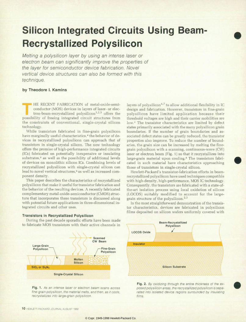
Transistors in Recrystal l ized Polysi l icon During the past decade sporadic efforts have been made
to fabricate MOS transistors with their active channels in
Scanned C W B e a m
Large-Grain Polysil icon Fine-Grain
Polysilicon
Single-Crystal Si l icon
F ig . 1 . As an i n tense l ase r o r e lec t ron beam scans ac ross f ine-grain po/ysi l icon, the material melts, and then, as i t cools, recrystal l izes into large-grain polysi l icon.
layers of polysilicon4'7 to allow additional flexibility in 1C design and fabrication. However, transistors in fine-grain polysilicon have limited application because their threshold voltages are high and their carrier mobilities are low.4 The transistor characteristics are limited by defect states primarily associated with the many polysilicon grain boundaries. If the number of grain boundaries and as sociated defect states can be greatly reduced, the transistor properties also improve. To reduce the number of bound aries, the grain size can be increased by melting the fine- grain polysilicon with a scanning, continuous-wave (CW) laser or electron beam (Fig. 1) so that it recrystallizes into large-grain material upon cooling.8 The transistors fabri cated in such material have characteristics approaching those of transistors in single-crystal silicon.
Hewlett-Packard's transistor-fabrication efforts in beam- recrystallized polysilicon have used techniques compatible with high-density, high-performance, MOS 1C technology. Consequently, the transistors are fabricated with a state-of- the-art isolation process using local oxidation of silicon (LOCOS) suitably modified to account for the large- grain structure of the polysilicon.2'3
In the most straightforward demonstration of the transis tor characteristics, devices are fabricated in polysilicon films deposited on silicon wafers uniformly covered with
Beam-Rec rys ta l l i zed Polysilicon
Si
F ig . 2 . By ox id i z ing th rough the en t i re th i ckness o f t he ex posed polysi l icon areas, the recrystal l ized polysi l icon is sepa ra ted in to i so la ted dev ice reg ions sur rounded by insu la t ing films.
1 0 H E W L E T T - P A C K A R D J O U R N A L A U G U S T 1 9 8 2
© Copr. 1949-1998 Hewlett-Packard Co.

insulating layers. The polysilicon is melted using an argon-ion C\V laser to convert the initial fine-grain polysili con to large-grain material (Fig. 1). A layer of silicon nitride is deposited over a thin stress-relief oxide layer and pat terned to retain the nitride in the active device regions. The exposed polysilicon areas are oxidized until the growing oxide reaches the insulating layer beneath the polysilicon. Each device island of polysilicon is thus completely iso lated from adjacent islands and from the substrate by in sulating layers (Fig. 2). Alternatively, the polysilicon be tween device islands could be removed by etching.
The remaining steps of the transistor-fabrication process are similar to those used to form silicon-gate transistors in single-crystal silicon. A schematic cross section of a finished transistor is shown in Fig. 3. In some cases, the threshold voltage is adjusted by implanting boron or phos phorus through the gate oxide before the gate polysilicon is deposited. Ion-implanted source and drain regions are used and the heat treatment after these implantations is limited to avoid excessive diffusion.
Fig. 4 shows the source-drain characteristics of large- and small-geometry, n-channel, recrystallized polysilicon transistors, as well as single-crystal-silicon and fine-grain polysilicon devices. The kink in the current -vers us- voltage characteristic arising from the presence of the insulator under the channel region is clearly seen for the large- geometry transistor. Some p-channel transistors have also been fabricated, and transistors with effective channel lengths as short as 1 /¿m have been obtained. Transistors in polysilicon recrystallized using an electron beam have characteristics similar to those in laser-recrystallized polysilicon.3
Use of Beam-Recrystal l ized Devices in Si l icon ICs The characteristics of recrystallized polysilicon transis
tors can be useful in many 1C applications that normally use single-crystal-silicon transistors. The carrier mobilities are generally about half those of single-crystal transistors, but about five to twenty times larger than those of transistors in fine-grain polysilicon (Table I). The threshold voltages of the recrystallized transistors are only slightly greater than those or single-crystal transistors, rather than being 10 or
Deposited Oxide Aluminum
Source Drain
Fig. in Schemat ic c ross sect ion o f a t rans is tor fabr ica ted in recrystal l ized polysi l icon.
Tab le I Character ist ics of MOS Transistors Fabricated in
Single-Crystal Si l icon and Polysi l icon
n-Channel p-Channel
M o b i l i t y V T M o b i l i t y Y T ( c m 2 / V - s ) ( V ) ( c m W - s ) ( V )
S i n g l e - c r y s t a l s i l i c o n 6 7 0 1 1 8 0 - 1 . 5
L a s e r - r e c r y s t a l l i z e d 3 0 0 1 t o 2 1 2 0 - 2 polysilicon
F i n e - g r a i n p o l y s i l i c o n = 1 0 t o 2 0 = 1 0 = 2 0 = - 1 0 t o 2 0 t o - 2 0
20V higher, as in fine-grain polysilicon transistors. In addi tion, the source-to-drain leakage current of transistors with short (1 to 2 /¿m) channels is in the range of 1CF13 am peres per micrometer of channel width, not very different from that of single-crystal transistors.
Once discrete transistors and simple ring oscillators had been wa in recrystallized polysilicon on silicon wa fers uniformly covered with insulating layers, we wanted to combine the polysilicon transistors with those fabricated in adjacent regions of single-crystal silicon. In one potentially beneficial application, p-channel transistors can be fabri cated in recrystallized polysilicon and combined with high-performance, n-channel transistors in adjacent re gions of the single-crystal silicon substrate to form a CMOS integrated circuit.
CMOS ICs are becoming increasingly important for the realization of low-power, high-speed functions. While CMOS is generally easy to use, the possibility of latch-up (undesirable large lateral current flow between adjacent complementary devices triggered by some circuit condi tions), and the resulting loss of circuit control, may restrict its use. The various techniques that have been used to minimize latch-up may significantly increase the chip size and are, consequently, less than ideal.
Completely separating the two polarities of devices by use of oxide layers totally avoids latch-up, but such com plete oxide isolation previously required very difficult processing. Using the new, recrystallized-polysilicon ap proach, both process simplification and control can be ob tained. One type of transistor is fabricated in the single- crystal substrate, and the other type is formed in a layer of recrystallized polysilicon separated from the single-crystal substrate by an insulating oxide layer.
Placing one type of device in the single-crystal substrate and the other in the polysilicon layer provides the addi tional advantage of optimizing the characteristics of the most critical transistor. For optimum circuit performance p-channel transistors are fabricated in a layer of laser- recrystallized polysilicon while n-channel transistors are constructed in adjacent regions of the underlying single- crystal substrate. To simplify the processing and allow the use of existing masks, the transistors are separated laterally, rather than being stacked with a common gate. Fig. 5 schematically shows the cross section of such a transistor
AUGUST 1982 HEWLETT-PACKARD JOURNAL 11
© Copr. 1949-1998 Hewlett-Packard Co.

(b)
L = 4 / * m W = 5 M m * * Ten 2V Ga le S teps
(Note expanded vert ical current scale)
Fig . (b ) t rans is to rs charac te r i s t i cs o f (a ) la rge-geomet ry and (b ) sma l l -geomet ry t rans is to rs fabricated in recrystal l ized poly si l icon, along with the characterist ics of (c) single-crystal-si l icon
and (d) f ine-grain-polys i l icon t ransistors (see reference 2) .
pair. Both n-channel and p-channel, large-geometry transis
tors exhibit well behaved saturation regions with square- law characteristics. Threshold voltages are approximately IV for the single-crystal, n-channel transistors and -2V for the recrystallized-polysilicon, p-channel transistors. Car rier mobilities are 670 and 120 cm2/V-s, as expected for the two types of transistors.
Several different, fifteen-stage ring oscillators were fabri cated. Their oscillation periods agree well with the times calculated to charge the capacitance associated with switching a stage. These switching times were calculated from the transistor geometries of each different ring oscil lator and the characteristics of discrete transistors. Some of the capacitances that must be charged are markedly lower than in single-crystal circuits because the oxide under the p-channel transistors has a dielectric constant one-third that of silicon.
Future Trends Future efforts can be directed along several paths. Dem
onstration of integrated circuits with transistors in the single-crystal silicon substrate and in layers of recrystal l ized in opens the poss ibi l i ty of s ignif icant ly in creased component density, as well as removing some cir cuit performance limitations (e.g. eliminating the possibil ity of latch-up in CMOS structures). In addition to improved density, novel structures can be obtained by using interac tions in the vertical direction. For example, CMOS gates have been fabricated with a single gate electrode control ling a transistor of one type in the underlying single-crystal substrate and a transistor of the opposite type in recrystal lized polysilicon above the gate electrode.6 The extension to other novel, vertical 1C structures offers exciting pos sibilities for "vertical integration."
Although the transistors in recrystallized polysilicon have characteristics approaching those of single-crystal transistors, the few remaining grain boundaries can limit device performance. Removing these grain boundaries by seeding the regrowth of the silicon layer through periodic contact between the polysilicon and the underlying single-
1 2 H E W L E T T - P A C K A R D J O U R N A L A U G U S T 1 9 8 2
© Copr. 1949-1998 Hewlett-Packard Co.

p-Channel Transistor
- n
Recrystal l ized Polysil icon
n-Channel Transistor
Single-Crystal Sil icon
Fig. 5. Schematic cross sect ion of a CMOS transistor pair used in an in tegra ted c i rcu i t . Any poss ib i l i t y o f l a t c h - u p i s a v o i d e d b y c o m p l e t e l y s u r r o u n d i n g o n e t y p e o f t r a n s i s t o r b y i n s u l a t i n g s i l i c o n dioxide.
crystal substrate (Fig. 6) can enhance the transistor per formance.9'10
Fabricating MOS transistors with their channels in re- crystallized polysilicon offers the most exciting and poten tially useful application of beam-recrystallization technol ogy. However, several more-straightforward applications should be mentioned. The ease of implementing these would lead to a more immediate impact on 1C technology. For example, recrystallization of polysilicon may make the resistivity of high-valued resistors used in static RAMs less sensitive to slight variations in dopant concentration.11 Melting only the top region of a polysilicon layer may smooth its surface, allowing the formation of higher-quality thermal oxides for double-level polysilicon-gate MOS ICs.12 Finally, the use of other heat sources to melt the polysilicon, such as black-body radiation,13'14 may sim plify recrystallization.
Acknowledgments The author would like to thank D. Ilic, F. Schwettmann,
and J. Moll for their ideas and encouragement during this investigation and the other members of the beam- recrystallization project: C. Drowley, P. Zorabedian, and C. Heimberg.
References 1. K.F. Lee, et al , "Thin Film MOSFETs Fabricated in Laser- Annealed Polycrystalline Silicon," Applied Physics Letters, Vol. 35, July 15, 1979, p. 173. 2. T.I. Kamins, et al, "A Monolithic Integrated Circuit Fabricated in Laser-Annealed Polysilicon," IEEE Transactions on Electron Devices, Vol. ED-27, January 1980, p. 290. 3. T.I. Kamins and B.P. Von Herzen, "MOSFETs in Electron-Beam
Recrystallized — , S i n g l e - C r y s t a l /
S i l i c o n F i l m /
Scanned CW Beam
Seeding Region
Single-Crystal Si l icon Substrate
Fig. 6 . S ing le-crysta l reg ions of s i l icon are formed by "seed ing" the regrowth of a polysi l icon layer using per iodic contact between the layer and the underlying, single-crystal substrate.
Recrystallized Polysilicon," IEEE Electron Device Letters, Vol. EDL-2, December 1981, pp. 313-315. 4. T.I. Kamins, "Field-Effects in Polycrystalline-Silicon Films," Solid-State Electronics, Vol. 15, 1972, pp. 789-799. 5 . T . I . K a m i n s a n d P . A . P i a n e t t a , " M O S F E T s i n L a s e r - Recrystallized Polysilicon on Quartz," Electron Device Letters, Vol. EDL-1, October 1980, pp. 214-216. 6. J.P. Colinge and E. Demoulin, "A High-Density CMOS Inverter wi th Vol . T rans i s to r s , " IEEE Elec t ron Dev ice Le t t e r s , Vo l . EDL-2, October 1981, pp. 250-251. 7. C.H. Fa and T.T. Jew, "The Polysilicon Insulated-Gate Field- Effect Transistor," IEEE Transactions on Electron Devices, Vol. ED-13, February 1966, pp. 290-291. 8. A. Crys etal,,"CW Laser Anneal of Polycrystalline Silicon: Crys talline Structure, Electrical Properties," Applied Physics Letters, Vol. 33, October 15, 1978, p. 775-778. 9. M. Tamura, H. Tamura, and T. Tokuyama, "Si Bridging Epitaxy from Si Windows onto SiO2 by Q-Switched Ruby Laser Pulse An nealing," Japanese Journal of Applied Physics, Vol. 19, January 1980, pp. L23-26. 10. T.I. Kamins, et al, "Lateral Epitaxial Recrystallization of Depo s i ted Si l icon Fi lms on Si l icon Dioxide," Journal of the Elec trochemical Society, Vol. 128, May 1981, pp. 1151-1154. 11. G. Yaron, L.D. Hess, and G.L. Olson, "Electrical Characteristics of Laser-Annealed Polysilicon Resistors for Device Applications," in Laser and Electron Beam Processing o/MateriaJs, edited by C.W. White and P.S. Peercy, Academic Press, 1980, pp. 626-631. 12. G. Yaron, L.D. Hess, and S.A. Kokorowski, "Application of Laser Processing for Improved Oxides Grown from Polysilicon," IEEE Transactions on Electron Devices, Vol. ED-27, May 1980, pp. 964-969. 13. J.C.C. Fan, M.W. Geis, and B.-Y. Tsaur, "Lateral Epitaxy by Seeded Solidification for Growth of Single-crystal Si Films on Insulators," Applied Physics Letters, Vol. 38, March 1, 1981, pp. 365-367. 14 . B . -Y. Tsaur , e t a l , " Improved Techniques for Growth of Large-Area Single-Crystal Si Sheets Over SiOa Using Lateral Epitaxy by Seeded Solidification," Applied Physics Letters, Vol. 39, October 1, 1981, pp. 561-563.
Theodore I . Kamins Ted Kamins is an author or co-author of 52 articles, many on polycrys- ta l l ine s i l icon. He is a co-author of a book, Device Electronics for Integrated Circuits, and is named inventor on f ive patents related to 1C technology. Ted jo ined HP in 1974 wi th severa l years o f exper i ence the materials and device R&D work. He is a project leader in the In tegrated Ci rcu i t Laboratory o f HP Laborator ies. Ted holds BS (1 963), MS (1964), and PhD (1 968) degrees in electrical engineering awarded by the Univers i ty o f Cal i forn ia a t Berke ley, where he has held served position of acting assistant professor. He has also served as a v is i t ing lecturer a t Stanford Univers i ty . Ted is a member of the Elect rochemical Society and a Senior Member of the IEEE.
AUGUST 1982 HEWLETT-PACKARD JOURNAL 13
© Copr. 1949-1998 Hewlett-Packard Co.
X-Ray Lithography The shor ter wavelengths of sof t X-ray radiat ion make the def in i t ion of even smal ler d imensions for VLSI c i rcui ts possib le.
by Garre t t A . Garre t tson and Armand P . Neukermans
X-RAY LITHOGRAPHY is proximity printing using a quasi-point source of soft (0.25 to 3.0 keV) X-rays. The important elements of an X-ray exposure sys
tem are illustrated in Fig. I. X-rays are generated in an evacuated area by electron bombardment and penetrate a thin (25 to 50 /urn) beryllium window. They are shadowed by a mask consisting of an absorber pattern supported on a flat membrane (5 to 10 /txm thick) that is relatively transpar ent to the radiation. The mask is accurately positioned parallel to the wafer and in close proximity (typically 10 to 100 /jon) with it. The wafer is coated with an X-ray-sensitive resist. The space between the X-ray source and the mask (working distance D) is evacuated or filled with helium to reduce attenuation of the radiation.
X-Ray Source High-energy (10 to 30 keV) electron bombardment
sources are commonly used to generate the required soft X-ray radiation. Other sources such as synchrotron radia tion, plasma pinch, and laser plasmas are being considered, but presently their application to integrated circuit lithog raphy is either prohibitively expensive or needs further development.
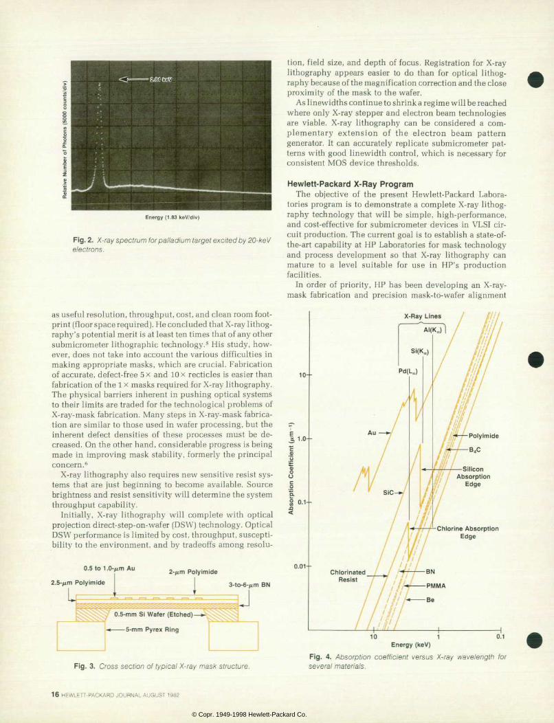
A typical measured spectrum from 20-keV electron bombardment of palladium (Pd) is illustrated in Fig. 2. The desired characteristic radiation under the peak (2 . 84 keV) is caused by electronic transitions in the La shell of a pal ladium atom. The remaining continuum spectrum is caused by the deceleration of electrons interacting with the Pd target atoms. Although the continuum spectrum does provide some additional exposure energy, its predomi nantly higher-energy X-rays are weakly absorbed, tending to produce an undesirable reduction of exposure contrast. Maximum source brightness (maximum power and minimum spot size) are factors determined by the electron optics, the characteristics of the anode (melting point, vapor pressure, elastic strength), and the performance of the cooling system.
Mask and Resist The X-ray mask is the most critical structure in the sys
tem. The membrane (pellicle) supporting the absorber pat tern must be made of a thin, low-atomic-number material to minimize X-ray attenuation, and yet must remain stable to minimize distortions caused by stresses in the absorber pattern. Typically the pellicle is stretched across a stiff, flat ring whose expansion coefficient matches that of silicon. This is essential to achieve good gap control between the
mask and the wafer and to alleviate the requirement for absolute temperature control. To first order, the absorber pattern and the wafer should expand and contract at the same rate.
A typical mask structure is shown in Fig. 3. Factors im portant to mask fabrication are pattern accuracy, absorber line-edge profile, and defect density.
Whereas for optical masks the transmission through clear and opaque areas may differ by orders of magnitude, for X-ray masks the transmission may only differ by approxi mately a factor of ten. For good contrast the absorber mate rial is made as thick as possible (typically 0.1 to 1.0 /¿m of gold). Hence submicrometer linewidths result in absorber pattern aspect ratios (thickness divided by lateral dimen sion) approaching unity, which require considerable exper tise in fabrication. A careful tradeoff must be made among the source energy spectrum, mask transmission and con trast, and absorption in the X-ray resist.
Presently, for state-of-the-art integrated circuit lithog raphy (minimum feature size of 0. 5 to 1 .0 ¿tm) , the combina tion of Pd-La radiation, a boron-nitride mask pellicle, a gold absorber pattern, and a resist containing chlorine appears most effective. The fortuitous position of the Pd-La peak with respect to the chlorine absorption edge (Fig. 4) and the symbiotic effect of this halogen, which increases both ab sorption and resist speed, make a powerful combination.1 For higher-resolution lithography, characteristic radiation softer than Pd-La can be used to reduce the required ab sorber thickness and increase absorption in the resist at the expense of reduced X-ray energy at the wafer.
Alignment Given an accurate mask pattern there must be a consistent
mechanical means for positioning it with respect to the wafer to insure level-to-level alignment accuracy. This re quires position references on the mask and on the wafer, as well as an alignment scheme. As illustrated in Fig. Ib, the mask-to-wafer gap can be adjusted to compensate for linear distortion of the wafer or the mask caused by process- induced strain. This is a significant advantage that allows good layer-to-layer alignment over larger fields than would be possible otherwise. Reproducible mask-to-wafer gap control is essential for accurate alignment. For this reason the mask plane must be flat to better than a micrometer and the wafer topography must be kept consistent each time the wafer is pulled down on the vacuum chuck. Dirt between the chuck and the wafer can result in surface bumps unless the chuck is designed to minimize the contact area. For this
1 4 H E W L E T T - P A C K A R D J O U R N A L A U G U S T 1 9 8 2
© Copr. 1949-1998 Hewlett-Packard Co.

Anode Coolant
Palladium Anode (Projected Source Diameter S)
Electron Gun
igh Voltage
Ion Pump Port
Chamber Coolant
(a) Magnification
A=R(g/d)
Mask: Pellicle Absorber
Y-Driver—
Z- Drive r
Fig. 1. section X-ray l i thography system. Close-up views of mask-to-wafer cross section showing (a) magni f ica t ion and (b) penumbra l shadow er rors .
reason a "bed-of-nails" design using many small contact areas is preferred.2
Tradeoffs The perceived advantages of X-ray lithography have been
its extreme fine-line capability (because of the absence of diffraction and proximity effects3), uniform resist exposure that allows high resist aspect ratios, good linewidth control, and insensitivity to dirt. As the field develops the percep tion of the strengths of X-ray lithography relative to other microlithographic technologies is evolving.
There have been dramatic improvements in the last five years in the performance of optical lithography, principally through the use of projection/reduction steppers and mul
tilevel resist technologies. This performance comes, how ever, at considerable capital expense, reduced throughput, and increased processing complexity. The investment for an X-ray system is projected to be a fraction of that required for an optical stepper. Although many of the technologies involved are not easy to master, they are not necessarily expensive in their execution. High throughput is projected (20 to 100 wafer levels an hour), because of large subfields and relatively short exposure times (down to 20 seconds using a 4-kW source).4 Less stringent environmental re quirements and the potential for using single-level resists are additional advantages.
In a recent study, Lepselter computed a figure of merit for various lithographic systems, which included such factors
AUGUST 1982 HEWLETT-PACKARD JOURNAL 15
© Copr. 1949-1998 Hewlett-Packard Co.
Energy (1.83 keV/div)
Fig. 2. X-ray spectrum for pal ladium target exci ted by 20-keV electrons.
as useful resolution, throughput, cost, and clean room foot print (floor space required). He concluded that X-ray lithog raphy's potential merit is at least ten times that of any other submicrometer lithographic technology.5 His study, how ever, does not take into account the various difficulties in making appropriate masks, which are crucial. Fabrication of accurate, defect-free 5 x and 10 x recueles is easier than fabrication of the 1 x masks required for X-ray lithography. The physical barriers inherent in pushing optical systems to their limits are traded for the technological problems of X-ray-mask fabrication. Many steps in X-ray-mask fabrica tion are similar to those used in wafer processing, but the inherent defect densities of these processes must be de creased. On the other hand, considerable progress is being made in improving mask stability, formerly the principal concern.6
X-ray lithography also requires new sensitive resist sys tems that are just beginning to become available. Source brightness and resist sensitivity will determine the system throughput capability.
Initially, X-ray lithography will complete with optical projection direct-step-on-wafer (DSW) technology. Optical DSW performance is limited by cost, throughput, suscepti bility to the environment, and by tradeoffs among resolu-
0.5 to 1 .0-fim Au
2 . 5 - ^ m P o l y i m i d e 2-/um Polyimide
3-lo-6-fim BN
— ' — ü 0.5-mm Si Wafer (Etched)
5 - m m P y r e x R i n g
Fig. 3 . Cross sect ion of typ ica l X- ray mask s t ructure.
tion, field size, and depth of focus. Registration for X-ray lithography appears easier to do than for optical lithog raphy because of the magnification correction and the close proximity of the mask to the wafer.
As linewidths continue to shrink a regime will be reached where only X-ray stepper and electron beam technologies are viable. X-ray lithography can be considered a com plementary extension of the electron beam pattern generator. It can accurately replicate submicrometer pat terns with good linewidth control, which is necessary for consistent MOS device thresholds.
Hewlett -Packard X-Ray Program The objective of the present Hewlett-Packard Labora
tories program is to demonstrate a complete X-ray lithog raphy technology that will be simple, high-performance, and cost-effective for submicrometer devices in VLSI cir cuit production. The current goal is to establish a state-of- the-art capability at HP Laboratories for mask technology and process development so that X-ray lithography can mature to a level suitable for use in HP's production facilities.
In order of priority, HP has been developing an X-ray- mask fabrication and precision mask-to-wafer alignment
Energy (keV)
F ig . 4 . Abso rp t i on coe f f i c i en t ve rsus X - ray wave leng th fo r several materials.
1 6 H E W L E T T - P A C K A R D J O U R N A L A U G U S T 1 9 8 2
© Copr. 1949-1998 Hewlett-Packard Co.

Fig. 5. Photo of boron-ni t r ide pel l ic les.
capability, fast resist systems, a bright X-ray source, and laboratory exposure tools. The first-generation mask technology uses a pellicle of chemical-vapor-deposited boron nitride and polyimide supporting a sputter-etched gold absorber pattern (Fig. 3 and Fig. 5). This is bonded to a Pyrexâ„¢ring for mechanical and thermal stability. Initial tests indicate that presently the stability is adequate for design rules down to one micrometer. Other materials such as silicon carbide and boron carbide have been investigated for the mask pellicle and they show considerable promise for future applications.
Defect density remains a critical problem. With careful process control, defects have been reduced around two orders of magnitude in the past year. Two orders of mag nitude more will be required for VLSI.
A number of fast, chlorinated, negative resists have been evaluated. Fig. 6 (page 18) shows submicrometer features in 0.6 to 0.8 fiïn of remaining resist material that has been exposed about 4 minutes using a 4-kW source at a working distance of 35 centimeters. A fixed anode source of a modi fied Gaines design7 has been built (Fig. 1). With a propri etary cooling technology it appears that power densities greater than 40 kW/cm2 may be accommodated.
Several laboratory exposure systems have been built for evaluating resists, for mask development, and ultimately for 1C applications. The latest is a very compact automatic- alignment exposure system employing a novel mask-to- wafer positioning system with six degrees of freedom. A proprietary alignment scheme can resolve misalignments as small as 20 nanometers consistently, but the level-to- level alignment accuracy of the system has yet to be deter mined under realistic operating conditions.
Acknowledgments The authors acknowledge the support of their colleagues
in the Physical Electronics and Solid-State Laboratories of Hewlett-Packard Laboratories and thank them for their con tributions to the work described in this article.
References 1. A. Zacharias, "An X-Ray Lithography System for VLSI Device Fabrication," American Vacuum Society Proceedings: 15th Sym-
posium on Electron. Ion. and Photon Beam Technology. Boston. Massachusetts. 1979, p. 1953. 2. T.E. Saunders. "Wafer Flatness Utilizing the Pin-Recess Chuck." Solid State Technology. Vol. 25. no. 5. May 1982. pp. 73-76. 3 . P . by and M.P.C. Wat ts , "Proximi ty Effec t Correc t ion by Means of Processing: Theory and Applications." Hewlett-Packard Journal, Vol. 32, no. 12. December 1981. 4 . H . E l ec Ex t ended Abs t r ac t s . 161s t Mee t ing o f t he E l ec trochemical Society'. Vol. 82-1, Montreal, Canada. May 1982, p. 281. 5. The Rosen Electronics Letter, February 8, 1982. p. 7. 6 . B . o f and S . Jones . "X-Ray L i thography : Fabr i ca t ion o f Masks and VLSI Devices," Society of Photo-Optical Instrumenta tion Engineers Proceedings 333. San Jose, California. March 1982. 7. J. 1972, Gaines, Nuclear Instrumentation Methods. Vol. 102, 1972, pp. 7-12.
Armand P. Neukenmans ' A rmand Neuke rmans i s a p ro j ec t man
ager for X-ray l i thography at HP Labora tor ies . Born in Okegem, Be l gium, he received his BSME and BSEE degrees f rom Louvain Univers i ty in 1962, did engineering work for the next f ive years, and then returned to school, receiv ing h is MSEE degree f rom
| Ar izona State Universi ty (1967) and PhD degree in app l ied phys ics f rom Stanford Universi ty (1970). After three years of xerographic research, Armand joined HP ¡n 1973. Among his contribu tions are a cesium iodide X-ray imaging screen, an electron capture detectorfor
gas chromatography, and work on Monte Car lo s imulat ions for e lec t r on 13 exposu res . H i s wo rk has r esu l t ed i n t en pa ten t s and 13 papers. He is a member of the IEEE and Sigma XL Armand is married, has four chi ldren, and l ives in Palo Alto, Cali fornia. He teaches rel igi ous educat ion and en joys jogg ing, swimming, and h ik ing.
Garrett A. Garrettson Garry Garrettson is a native of California born in San Francisco. He at tended Stanford Universi ty, earning the BS (1965) and MS (1966) degrees ¡n en g ineer ing phys ics and the PhD (1969) degree in mechanical enginer ing. After a few years as an assistant professor at the U.S. Naval Postgraduate School , Garry jo ined HP Laborator ies in 1973. S ince then he has worked in areas of metrology, medical instrumentat ion, and photoconductor deve lopment . Gar ry p resent ly i s a depar tment man ager ¡n the Physical Electronics Laboratory of HP Laboratories and has
responsib ly for l i thography s t ra tegy and X-ray technology develop ment. He is the author or co-author of s ix publ icat ions re lated to t ransport theory and l i thography. Garry served several years in the U.S. Navy, at ta in ing the rank of l ieutenant . He is a member of the Amer ican Phys ica l Soc iety and the Amer ican Associat ion for the Advancement of Science. He is married , has two children, and lives ¡n Los Altos Hills, California. Outside of work, Garry coaches soccer and baseball and supports a Cub Scout group. He enjoys running, skiing, carpentry , and f ly ing (he has a commerc ia l p i lo t 's l icense wi th an instrument rating).
J t li, J
AUGUST 1982 HEWLETT-PACKARD JOURNAL 17
© Copr. 1949-1998 Hewlett-Packard Co.

9 2 5 1 2 2 0 K U 9 . 5 U
F ig . f r om by resu l t s i n f as t nega t i ve res i s t us i ng X - rays f r om Pd anode exc i t ed by 10 -keV electrons, a 25-tun-thick beryl l ium window, and a mask-to-wafer gap of 25 ¡Jim.
1 8 H E W L E T T - P A C K A R D J O U R N A L A U G U S T 1 9 8 2
© Copr. 1949-1998 Hewlett-Packard Co.

Dry Etching: An Overview Plasma etching technology has several advantages for 1C process ing compared to wet -chemica l e tch ing methods . An isot rop ic e tch ing and automat ic endpoin t detec t ion are two of the advantages d iscussed in th is ar t ic le .
by Paul J . Marcoux
ONE OF THE BASIC TRENDS in silicon integrated circuit process technology is the shrinking of de vice geometries. Recent advances in lithography
allow the patterning of feature sizes sufficiently small that conventional methods of etching are inadequate. During the past several years dry etching has evolved to the point where this etch process can transfer the lithographic pat tern to the device structure with high fidelity.
The process technique of dry etching has many varia tions. This technology ranges from processes in which the etching proceeds by a purely physical mechanism to cases in which chemical interactions dominate the etch. The most are dry etch processes for pattern replication are those in which chemical etching is enhanced by the physi cal component of the process. Ion milling and sputter etch ing techniques use momentum transfer from inert-gas ion bombardment as the physical etch mechanism. Reactive ion beam etching (RIBE, also reactive ion milling), reactive ion etching (RIE, also reactive sputter etching) and plasma etch ing all use reactive ions to transfer momentum to the sample and add a chemical component to the etching process. Table I provides a qualitative comparison of the dry etch technologies and conventional wet etch processing.
The key process characteristics associated with the plasma etch process are anisotropy and etch selectivity with respect to the photoresist mask and the underlying materials (etch stop). Fig. 1 shows a representation of a typical cross section of an etched sample.
The after-etch profile of a feature is the critical result of the plasma etch process. This profile indicates whether or not a particular etch process gives an isotropic (uniform in all directions) or anisotropic (direction-dependent) etch. In
-L2- - L , -
Etch Mask
Etched Film
Substrate
Fig. 1 . A typical cross section of an integrated circuit feature. For an anisotropic etch Li =¿.2 and Lz is not altered by the etch process. In most processes the ratio of the fi lm etch rate to the etch-stop-material etch rate varies from 5: 1 to 10:1. The ratio of the f i lm etch rate to the mask etch rate is s imi lar .
Table I
A Qualitative Comparison of Etching Methods for Sil icon Integrated Circuit Fabrication
Fig. 2 isotropic and anisotropic etch profiles are compared. For processes that produce an isotropic etch profile the reduction of linewidth is at least twice the film thickness. Since the linewidths of minimum-size features are typically two to four times the film thickness it is obvious why an isotropic etch is not useful. The only way to reproduce fine-line lithography is to use an anisotropic etch. Another important feature of an anisotropic etch is that generally there is no increased loss of linewidth control with over- etching. This is important because overetching is required in routine processing to ensure that all wafers in a load have been completely cleared during the etch process.
In ion milling and sputter etching, inert gas ions bombard the surface of the wafer and sputter away the surface atoms via momentum transfer. In ion milling, ions are extracted from an ion source, accelerated, and deionized before im pacting the surface being milled. In sputter etching, ions that bombard the surface are extracted from the gas glow discharge in which the wafers are immersed. In both of these methods the etching is quite anisotropic because the motion of the ions follows electric field lines that are per pendicular to the substrate. The etch selectivity for these processes is generally poor because the sputter yields for materials used in integrated circuit fabrication are similar. In addition, there is often redeposition of the sputtered material along the sidewalls of the lithographically defined pattern. In spite of these disadvantages these technologies are useful, particularly in the laboratory, because they can be used to pattern fine lines in a wide range of materials.
Reactive ion beam etching is an emerging technology that
AUGUST 1982 HEWLETT-PACKARD JOURNAL 19
© Copr. 1949-1998 Hewlett-Packard Co.

Photoresist Mask
Etched F i lm
Etch Stop
Substrate (c)
Substrate
is similar to ion milling except that the ions responsible for the sputtering action are also reactive. This approach has the advantage that the material being etched can be con verted to a volatile compound as well as sputtered. At this time if technology is mainly a laboratory tool. However, if the numerous equipment problems can be overcome it may see broader application.
The techniques of reactive ion etching and plasma etch ing have the widest range of commercial and laboratory applications. Both etching methods make use of a glow discharge to create the reactive etch species and the ions responsible for the etch process from the input gases. These reactive species and ions diffuse to the substrate surface where they react with the thin film to be etched. This etch reaction must produce a compound that is volatile; other wise the etch process will be quenched by a residue coating on the surface. It is also very important that the etch reaction be selective with respect to the mask material and the mate rials under the layer being etched. The principal hardware differences between these two technologies are that in reac tive ion etching the substrates are placed on the cathode and the gas pressure is low, while in plasma etching the wafers are placed on the anode and the gas pressure is somewhat higher. In most cases this results in higher ion energies and hence more momentum transferred to the surface in reac tive ion etching. Table II lists materials that have been e tched us ing plasma e tching a t Hewlet t -Packard Laboratories. It shows the versatility of this technology and indicates the possible reactive etch species and correspond ing volatile etch product for each material.
Reactors Commercially available plasma etch reactors range from
laboratory apparatus to highly automated reactors suitable for use in integrated circuit manufacturing. These reactors
F i g . 2 . C o m p a r i s o n o f t h e e t c h p r o f i l e s f o r i s o t r o p i c a n d a n i s o - t rop ic e tch ing, (a) Diagram of iso t ropic etch prof i le , (b) SEM photo g raph o f ac tua l i so t rop ic p ro f i l e , ( c ) D i a g r a m o f a n i s o t r o p i c e t c h prof i le , (d) SEM photograph of ac tual anisotropic prof i le.
are available in two basic configurations: barrel or parallel plate. The selection of the configuration depends upon the user's application. All reactors have the following basic components: reaction chamber, vacuum system, gas flow control, an RF power supply, and in most cases, automatic gas pressure control. In the more sophisticated reactors a microprocessor controls the gas flows, total pressure, and the vacuum values associated with the reactor. In many systems the wafer handling is also automated. An increas ing number of reactors have automatic process endpoint detection to determine when the etch process is complete (see box on page 22).
Table I I
Summary of P lasma Etch Processes
Etch Gas Composit ion
Material Etched
Resist
Si
SÃÃœ2
S Ã 3 N 4
W
Mo
T i
C r
Al
* Proceeds at elevated temperatures (T >100°C).
Reactive Species
Principal Etch Products
2 0 H E W L E T T - P A C K A R D J O U R N A L A U G U S T 1 9 8 2
© Copr. 1949-1998 Hewlett-Packard Co.
- W a f e r s -
(b)
Gas Inlet
.
To Vacuum Pump
Fig . 3 . D iagram o f bar re l p lasma r e a c t o r , ( a ) E n d v i e w , ( b ) S i d e view.
A typical barrel reactor (Fig. 3) has the advantage that large wafer loads are possible in a quite small reactor vol ume. Plasma etch processes in these reactors generally re sult in an isotropic etch. Hence the main application for these reactors is noncritical etching.
Two principal configurations for parallel plate reactors are shown in Fig. 4. In the plasma etch mode the wafers are placed on the anode. Plasma reactors typically operate in the gas pressure range of 100 to 1500 millitorr, the total gas flow rates are on the order of 38 to 1520 torr-liter/s and the RF power densities range up to 0.7 watts/cm2. The vacuum system required by these reactors has a rather high base pressure of approximately 10 millitorr.
In the reactive-ion-etch mode the wafers are placed on the cathode and the power densities range up to 2 watts/cm2. These reactors generally use low total gas flow rates of 0.76 to 7.6 torr-liter/s and the operating pressures are in the range of 10 to 50 millitorr. The vacuum system used by these reactors generally is capable of reaching an ultimate vac uum of 0.001 millitorr.
Fig. 4 shows parallel plate reactors in the batch configura tion. It is obvious that, as the wafer size increases, the throughput (wafers/hour) will decrease, and the total wafer area per load will decrease slightly. In response to this negative effect on throughput, a relatively new type of parallel plate reactor has become available — the single- w a f e r a d r e a c t o r . T h i s r e a c t o r h a s t h e a d vantage that wafer throughput is independent of wafer size, and hence there is an increasing wafer area throughput as the wafer size increases. To achieve adequate wafer throughput, however, the etch rates for materials must be quite high. This demands that the etch selectivity and anisotropy be higher in this single-wafer design than in a batch reactor to achieve comparable process performance. Thus the overall process control must be tighter in a single-wafer reactor than in a batch machine.
Processing Parameters Plasma etching is in general a very complex process. One
main reason is that there is a large parameter space that must be well controlled. Furthermore, despite an intense research effort by many laboratories, the interaction among different parameters is not well understood. However, one can make some generalizations about the effects of these parameters.
In a typical plasma etch system the parameters include gas mixture composition, RF power, total flow rate, gas pressure, and substrate temperature. The most important parameter is the composition of the etch gas. This parame ter determines whether a process will etch a given material, etch the material with the desired selectivity, and etch anisotropically. It is true that the other parameters can have a substantial effect on the particular process characteristics, but without the correct etch gas these properties cannot be achieved.
The RF power level has a strong influence on the etch rate. It is often observed that the etch rate increases with a linear to quadratic dependence on RF power. Increasing the RF power tends to result in an increased ionization of the etch gas and increases the sheath voltage. This increases the average energy of ions bombarding the wafer surface and thereby increases the anisotropy of the etch. The RF power level also controls the particular chemistry of an etch gas. This occurs because the RF power strongly influences the distribution of energy of the electrons and this determines what particular atoms, ions, and free radicals will be pro duced from a given etch gas.
The total gas flow rate and pressure determine the resi dence time of an ion or reactive species in the discharge. The residence time t is approximately given by the follow ing equation:
t = (V/F)(P/760)
Wafers - Discharge Region
Gas Inlet
(a)
T o V a c u u m Pumps
(b)
T o V a c u u m Pumps
F i g . 4 . D i a g r a m o f s i d e v i e w o f pa ra l l e l p l a te reac to rs i n (a ) t he p l a s m a m o d e a n d ( b ) t h e reac t i ve - ion -e tch mode. The gas f lows rad ia l ly inward over the wa f e r s t h a t a r e i n i n t i m a t e c o n t a c t wi th the plasma.
AUGUST 1982 HEWLETT-PACKARD JOURNAL 21
© Copr. 1949-1998 Hewlett-Packard Co.

An Automated Plasma Reactor
With the advent of computers having a higher performance-to- cos t ra t io and the need for more complex , t igh t ly cont ro l led 1C process ing s teps there has been an increase in the use of auto m a t e d p r o c e s s i n g e q u i p m e n t . S e v e r a l y e a r s a g o , a t e a m o f eng ineers in Hewle t t -Packard 's In tegra ted C i rcu i ts Process ing L a b o r a t o r y ( I C P L ) i n i t i a t e d a p r o j e c t t o d e v e l o p a n a u t o mated p lasma reactor to be in tegra ted in to the process cont ro l system (PCS). PCS is a network of computers involved in process control and wafer tracking.1 The project has bui l t two reactors for use in ICPL.
Funct iona l cont ro l fo r these sys tems is prov ided by memory- based HP 1000 Compu te r s i n t e r f aced t o t he p l asma reac to r s t h r o u g h d i g i t a l - t o - a n a l o g c o n t r o l l e r s . O p e r a t i o n a l c o m m a n d s e q u e n c e s a r e d o w n l o a d e d f r o m a c e n t r a l u s e r - c r e a t e d d a t a base and then sequent ia l ly executed by the local control comput er . F ive major sof tware rout ines (wafer handl ing, pressure, gas f low, o f power , and temperature) prov ide c losed- loop cont ro l o f wafer loading and the necessary plasma processing parameters. Th roughou t t he p rocess ing sequence , sys tem pe r fo rmance i s monitored and can be displayed in ei ther a text or graphic format at intervals of 5 to 60 seconds. Also available is a TRACE function t h a t a l l o w s s e q u e n t i a l s a m p l i n g o f u p t o 1 6 o f t h e m o n i t o r e d parameters and storage of th is in format ion in centra l data f i les. The data accumulated by TRACE can then be recovered in l is t or graphical form. In addi t ion, an automat ic endpoint detect ion sys tem has been insta l led which uses e i ther laser in ter ferometry or opt ical emission spectroscopy to determine etch complet ion. The system then calculates and executes the desired overetch before ext inguish ing the p lasma.
The design phi losophy behind these reactors has been to bui ld systems that provide a s imple- to-operate, repeatable product ion tool f lexible enough to be used for new process development. For rout ine processing, s tandard operat ions are automat ica l ly down loaded from the PCS central data base to the local controller when wafers are tracked into the reactor. The etch sequence is init iated by s imply press ing the START but ton. A l l p rocess gases are au tomatical ly purged from the reactor upon etch complet ion for user safety. Wafer handl ing by personnel is minimized by the system's automated casset te- to-casset te wafer loading capabi l i ty . A load- lock chamber houses the load ing mechan ism. Th is i so la tes the ma in r eac to r chamber and t hus m in im i zes p rocess va r i a t i ons c a u s e d b y a t m o s p h e r i c c o n t a m i n a t i o n . O p e r a t i n g s e q u e n c e s a n d p a r a m e t r i c s e t p o i n t s c a n b e e d i t e d t h r o u g h t h e d i s p l a y keyboard to prov ide the f lex ib i l i ty requ i red for deve lopment pur poses.
Acknowledgments Among the many who have contr ibuted the i r e f for ts to making
the automatic plasma reactor a working real i ty are Bi l l Goodman, John Youden, Mary Dryden, Gary Modrel l , Ulr ich Kaempf, Dennis H a r d i n g , S u b h a s h T a n d o n , C h r i s C l a r e , B o b S c h u c h a r d , M e l Jennings, and BobStarkovich. Recogni t ion a lso goes to Pat Cas t ro and Fred Schwet tmann for the i r suppor t o f the pro jec t .
Reference 1 . C . R . 6 " A P r o c e s s C o n t r o l N e t w o r k , " H e w l e t t - P a c k a r d J o u r n a l , V o l . 3 2 , n o . 6 June 1981.
-Susan Okada
where V is the reactor volume, F is the flow rate and P is the pressure in torr. The residence time determines the flat zone of a reactor, that is, the region over which the concentration of reactive species is nearly constant. The magnitude of this distance will determine the etch uniformity for a particular etch condition. The chemistry of the discharge is altered by the total gas pressure because pressure changes alter the gas phase chemistry. It is in the gas phase that the reactive etch species are produced, hence the influence of pressure on the chemistry of the etch process.
The substrate temperature has an influence on etch rate and selectivity, and if allowed to go as high as 150°C, will cause photoresist degradation. The etch rate R can be de scribed by the following expression:
R = A exp(-E/kT)
where A is a constant, E is activation energy, k is the Boltzman constant and T is the absolute temperature (K). The activation energy in this expression represents an aver age over the important kinetic process and typically lies in the range of 0.05 to 0.5 eV. It is clear from the above expres sion that temperature should be well controlled because of the exponential dependence.
Endpoint Detection Besides the large number of parameters discussed above
that must be well controlled, there are other parameters that are difficult to control in a routine processing environment (e.g., condition of the reactor walls). The variations in both the well controlled and poorly controlled variables lead to variations in the performance of the process, particularly in the reproducibility of the etch rate. The use of endpoint detection to determine when the etch process is complete eliminates the effects of these variations on the process performance. In addition, there is an increase in throughput because the tedious procedure of calibrating etch times can be eliminated.
Many different techniques have been used for endpoint detection. A summary of the methods, principles of opera tion, and measured values that have been investigated by Hewlett-Packard Laboratories is presented in Table III. Ob-
t 1 +
I
Ã̈ 1 i o
I
Endpoint
â € ” \ 1 2 . 0 3 . 0
Time (minutes) 4.0 5.0
F i g . 5 . A p l o t o f t h e e m i s s i o n i n t e n s i t y o f t h e 3 9 6 - n m - wavelength l ine of aluminum in normal ized uni ts versus t ime. The period of t ime before etching begins ( inhibi t ion period) is about one minute and the endpoin t occurs a t 5 .2 minutes.
2 2 H E W L E T T - P A C K A R D J O U R N A L A U G U S T 1 9 8 2
© Copr. 1949-1998 Hewlett-Packard Co.

Table III Tab le IV
Summary of Methods for Endpoint Detect ion in Plasma or React ive Ion Etching
Summary of Emission Wavelengths and the Emit t ing Species Monitored for Endpoint Detect ion
Method
Emission spectroscopy
Optical reflection
Mass spectroscopy
Impedance monitoring
Langmuir probe
Gas pressure
•Dependent on optics.
Measuring
Light emitted from discharge
Interference phenomena or changes in reflectivity
Gas composition
Impedance mismatch
Changes in electron density and average energy
Total pressure
Monitoring
Emission from reactive species and or etch products
Changes in film thickness
Etch products
Voltage change
Current from probe
Changes in total pressure
Endpoint
Average for a l l wafers
For one wafer only
Average for all wafers
Average for all wafers
Average for all wafers
Average for all wafers
Film Etched S p e c i e s M o n i t o r e d W a v e l e n g t h s ( n m )
viously from the endpoint data, all of the techniques pro vide an average etch rate. The optical reflection method, which monitors the change in film thickness, also serves as an in-situ etch-rate monitor for dielectric films.
Emission spectroscopy has the longest history of the methods described in Table III. There are many variations of the experimental apparatus using emission spectroscopy for endpoint detection. The essential feature of such an apparatus is that it be able to detect the particular wavelength of light emitted by either a reactive etch species or a volatile etch product. For purposes of endpoint detec tion, it can be assumed that the intensity of the emission line is proportional to the concentration of the reactive etch species or volatile etch product in the plasma. If one monitors a reactive etch species the intensity of the emis sion from the species should be less in the presence of the film to be etched than in its absence. Hence at endpoint there is an increase in the signal when monitoring a reactive etch species. Conversely there is a decrease in the signal when monitoring etch products. In most cases monitoring of an etch product is preferred, because one need only determine the presence or absence of the material responsi ble for the signal.
To demonstrate the usefulness of endpoint detection, consider the use of emission spectroscopy for endpoint detection and process monitoring of aluminum etching. The optical emission wavelength monitored is that of ele mental aluminum at 396 nm. The intensity of this line is proportional to the amount of aluminum being etched. A typical endpoint trace is given in Fig. 5. The rise of the aluminum signal indicates the start of the etch process. It does not occur at t=0 because there is an inhibition period with this process. The inhibition period occurs because of
residual moisture and oxygen in the reactor, photoresist scum, and the presence of a native oxide layer on the aluminum film. One cause of irreproducibility in an aluminum etch process is variation in the inhibition period from run to run. The magnitude of the emission signal is proportional to the etch rate of aluminum. The length of the plateau region is determined by the etch rate and the thick ness of the aluminum layer. The decrease in the signal is a result of clearing the wafer; the steeper the descent the more uniform the etch process. The arrow indicates the endpoint of the etch process. As is typically the case some overetch- ing is done to insure a complete etch. From this example it is clear that, in addition to endpoint data, detailed informa tion on the performance of the process is obtained. This type of information is invaluable in a routine processing environment. A summary of emission wavelengths that have been found useful for endpoint detection is presented in Table IV.
Acknowledgments The author would like to thank his colleagues, Dragan
Ilic, Glenn Rankin, Pang Dow Foo, Bob Gleason, and Susan Okada for their help and stimulating discussions. Thanks are due to Fred Schwettmann, Pat Castro, and Bob Grimm for their support and encouragement during the course of this work. Special thanks are due to Frank Perlaki for the microphotographs that appear in this paper.
Paul J. Marcoux Paul Marcoux is the manager o f HP Laboratories' multi level metall ization 1C pro jec t . He prev ious ly managed a dry etching project . His contr ibut ions have resu l ted in 12 papers on gas phase k inet ics and p lasma process ing. Paul came to HP in 1978 a f te r do ing pos t doctoral research in chemistry. He was awarded a BS degree in chemis t ry by Vi l lanova Universi ty in 1970 and a PhD degree in chemis t ry by Kansas Sta te Universi ty in 1975, and is a member of the Amer ican Chemica l Soc ie ty , the Amer ican Vacuum Soc ie ty , and S igma XL Born in Pawtucket , Rhode Is land,
Paul is married, has one child, and l ives in Mountain View, California.
AUGUST 1982 HEWLETT-PACkARD JOURNAL 23
© Copr. 1949-1998 Hewlett-Packard Co.

Thin Films Formed by Plasma Enhanced Chemical Vapor Deposition Elect r ica l ly exc i t ing the gases used in a chemica l vapor depos i t ion process can reduce the sens i t iv i ty to temperature var ia t ions and a l low deposi t ion at lower temperatures. Some f i lms produced by th is technique are d iscussed.
by Dragan B. l l ic
PLASMA ENHANCED (PE) deposition of thin films has important advantages over conventional tech niques used in silicon integrated circuit process
ing. Conventional atmospheric- or low-pressure (AP orLP) chemical vapor deposition (CVD) techniques form thin films by using the nucleation of atoms and molecules from the gas phase at the substrate (wafer) surface. This nuclea tion reaction is thermally driven, and thus is a very sensi tive function of the wafer temperature. By contrast, in a gaseous plasma the chemical reactions are no longer ther mally controlled so that effective film deposition can take place at temperatures far below those needed for APCVD or LPCVD.
Hence, one important advantage of PECVD is a relative insensitivity to wafer temperature. Depositions can take place in a wide temperature range from 20°C to the tempera tures used in conventional CVD processes. However, PECVD films often are not stoichiometric, and have been found to contain large quantities of hydrogen incorporated from the process gases (usually hydrogen-based com pounds of silicon, nitrogen, and carbon). These characteris tics are manifested by large residual stresses built into these films as they are deposited. It is not unusual to have com- pressive or tensile stresses as large as 1000 atmospheres (109 dynes/cm2), depending on plasma characteristics, pro cess gas mixture, and wafer temperature. For good adhesion and crack resistance, a compressive stress is desirable.
There are numerous PECVD systems available commer cially that produce good quality films suitable for 1C passi vation (silicon nitride) or dielectric intermediate levels (silicon oxide or nitride) in multilevel interconnection schemes. For VLSI production applications, a high wafer throughput, good uniformity, and low particle density are all important requirements. Reported here are the results of initial applications of films developed in a modern PECVD reactor, whose design is an outgrowth of the standard LPCVD systems. Uniformity of the deposited film thickness and the refractive index of the film material were checked by ellipsometry and spectrophotometry. The stress built into each deposited film was deduced by comparing the wafer curvature before and after film deposition (see box, next page).1'2 All of the deposited films studied were
"Some of the data presented here has been previously d iscussed by the author in the Apr i l 1982 issue of Sol id State Technology.
found to have compressive stresses.
PECVD System The PECVD system used at Hewlett-Packard Laboratories
(HPL) was made by a commercial vendor of semiconductor manufacturing equipment. This system has been operating since July 1980, and proven to be sufficiently flexible to accommodate a wide range of different thin-film- deposition experiments. The system contains two com pletely independent thin-film-deposition systems, housed in a single frame.3
10
9
8
7
8- •
_ 5 g
o . c 4 >. •o & w _
I 55 2 . 5 - -
2 -
1.5 --
1.2 --
••
V • Parallel to Wafer Flat
Perpendicular to Wafer Flat
A
f V
1 2 3 4 Process Gas Pressure ( torr)
Fig. 1 . The var iat ion of stress measured in standard s i l icon- n i t r ide f i lms as a funct ion of process gas pressure.
2 4 H E W L E T T - P A C K A R D J O U R N A L A U G U S T 1 9 8 2
© Copr. 1949-1998 Hewlett-Packard Co.
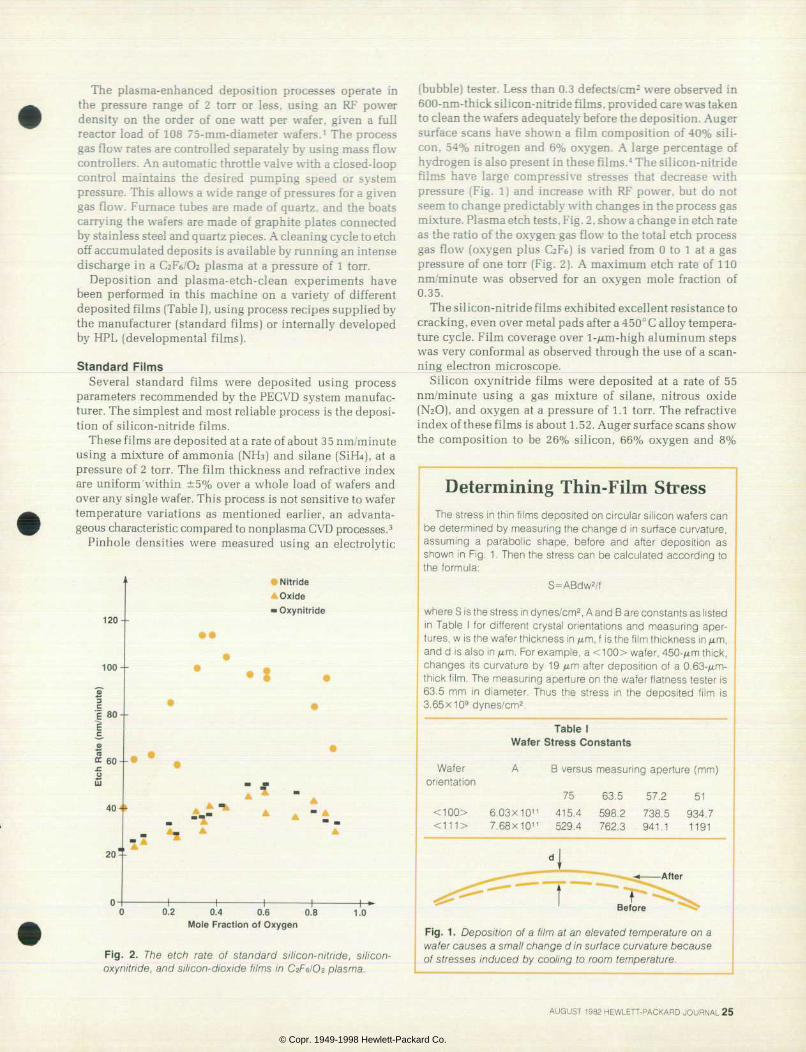
The plasma-enhanced deposition processes operate in the pressure range of 2 torr or less, using an RF power density on the order of one watt per wafer, given a full reactor load of 108 75-mm-diameter wafers.1 The process gas flow rates are controlled separately by using mass flow controllers. An automatic throttle valve with a closed-loop control maintains the desired pumping speed or system pressure. This allows a wide range of pressures for a given gas flow. Furnace tubes are made of quartz, and the boats carrying the wafers are made of graphite plates connected by stainless steel and quartz pieces. A cleaning cycle to etch off accumulated deposits is available by running an intense discharge in a CiFi/Oi plasma at a pressure of 1 torr.
Deposition and plasma-etch-clean experiments have been performed in this machine on a variety of different deposited films (Table I), using process recipes supplied by the manufacturer (standard films) or internally developed by HPL (developmental films).
Standard Fi lms Several standard films were deposited using process
parameters recommended by the PECVD system manufac turer. The simplest and most reliable process is the deposi tion of silicon-nitride films.
These films are deposited at a rate of about 3 5 nm/minute using a mixture of ammonia (NHa) and silane (SiFk), at a pressure of 2 torr. The film thickness and refractive index are uniform 'within ±5% over a whole load of wafers and over any single wafer. This process is not sensitive to wafer temperature variations as mentioned earlier, an advanta geous characteristic compared to nonplasma CVD processes.3
Pinhole densities were measured using an electrolytic
Nitride A Oxide • Oxynitride
120 - -
100 --
E 80 - -
6 0 - -
4 0 - -
2 0 - -
* ^
0 . 2 0 . 4 0 . 6 0 . 8 Mole Fract ion of Oxygen
1.0
(bubble) tester. Less than 0.3 defects/cm2 were observed in 600-nm-thick silicon-nitride films, provided care was taken to clean the wafers adequately before the deposition. Auger surface scans have shown a film composition of 40% sili con. 54% nitrogen and 6% oxygen. A large percentage of hydrogen is also present in these films.4 The silicon-nitride films have large compressive stresses that decrease with pressure (Fig. 1) and increase with RF power, but do not seem to change predictably with changes in the process gas mixture. Plasma etch tests, Fig. 2, show a change in etch rate as the ratio of the oxygen gas flow to the total etch process gas flow (oxygen plus CaFe) is varied from 0 to 1 at a gas pressure of one torr (Fig. 2). A maximum etch rate of 110 nm/minute was observed for an oxygen mole fraction of 0.35.
The silicon-nitride films exhibited excellent resistance to cracking, even over metal pads after a 450° C alloy tempera ture cycle. Film coverage over l-/«n-high aluminum steps was very conformal as observed through the use of a scan ning electron microscope.
Silicon oxynitride films were deposited at a rate of 55 nm/minute using a gas mixture of silane, nitrous oxide (N2O), and oxygen at a pressure of 1.1 torr. The refractive index of these films is about 1.52. Auger surface scans show the composition to be 26% silicon, 66% oxygen and 8%
Determining Thin-Film Stress The stress in thin f i lms deposited on circular si l icon wafers can
be determined by measur ing the change d in sur face curvature, a s s u m i n g a p a r a b o l i c s h a p e , b e f o r e a n d a f t e r d e p o s i t i o n a s shown to Fig. 1. Then the st ress can be calculated according to the formula:
S=ABdw2/ f
where S is the stress in dynes/cm2, A and B are constants as listed in Tab le I fo r d i f fe rent c rys ta l o r ien ta t ions and measur ing aper tures, w is the wafer thickness in /¿m, f is the film thickness in /urn, and d is also in /urn. For example, a <100> wafer, 450-j ixm thick, changes i ts curvature by 19 ¿im after deposit ion of a 0.63-ju.m- thick f i lm. The measuring aperture on the wafer f latness tester is 63 .5 mm in d iame te r . Thus the s t ress i n t he depos i t ed f i lm i s 3.65X10⁹ dynes/cm2.
Table I Wafer Stress Constants
Wafer orientation
B versus measur ing aper ture (mm)
A f t e r
F i g . 2 . T h e e t c h r a t e o f s t a n d a r d s i / i c o n - n i t r i d e , s i / i c o n - oxyni t r ide, and si l icon-dioxide f i lms in CzFslO? plasma.
Fig. 1 . Deposi t ion of a f i lm at an e levated temperature on a wafer causes a smal l change d in sur face curvature because o f s t resses induced by coo l ing to room temperature . of
AUGUST 1982 HEWLETT-PACKARD JOURNAL 25
© Copr. 1949-1998 Hewlett-Packard Co.

Thin Gate Dielectric Films for VLSI MOS ICs: Thermal Silicon Oxynitride
In sca l ing down the la tera l feature s izes o f in tegrated c i rcu i t dev ices to VLSI d imensions, the scal ing of the ver t ica l features must a lso be cons idered. In par t icu lar , the gate d ie lec t r ic th ick ness in MOS devices must be reduced substant ia l ly to mainta in constant power densi ty and increase c i rcu i t speed. As the chan n e l l e n g t h o f a n M O S t r a n s i s t o r i s r e d u c e d t o l e s s t h a n o n e mic rometer , the appropr ia te ga te d ie lec t r i c th ickness becomes as thin as 1 0 nanometers (approximately 30 to 40 atomic layers of material).
Severe demands wi l l be placed on this very thin gate dielectr ic f i lm. I t must demonstrate a h igh degree of uni formity and consis tency among its chemical, physical and electrical properties among devices, wafers and product ion runs. I t must remain e lect r ica l ly stable and relat ively nonconductive even when stressed with high electr ic f ields. I t must act as a strong di f fusion barr ier to contami nants the would otherwise diffuse from the gate electrode into the ac t i ve channe l reg ion and degrade t rans is to r pe r fo rmance . F i na l l y , t he f i lm mus t be i n t r i ns i ca l l y de fec t - f ree (on a pe r -a rea basis) and remain defect- f ree dur ing the r igors of 1C processing so that a h igh dev ice y ie ld can be main ta ined.
Tradit ional ly, thermal ly grown si l icon dioxide has been used as a v iable gate dielectr ic mater ia l at th icknesses down to about 25 to 30 nanometers. There is evidence, however, that when scaled down to 10 nanometers , thermal ox ide wi l l not meet the requi re ments of a good gate dielectr ic mater ial , part icular ly in the areas of intr insic defect density, durabi l i ty dur ing processing, and resis tance gate contaminant di f fusion. Therefore, other potent ia l gate d ie lect r ic mater ia ls have been invest igated as rep lacements for thermal ox ide in sca led dev ices.
The most p romis ing new gate d ie lec t r ic mater ia l i s thermal ly grown s i l icon oxyni t r ide, which is typical ly produced by react ing ammonia and oxygen with the si l icon substrate. A variety of chem ica l compos i t ions can be produced, pr imar i ly dependent on the rat io o f ammonia to oxygen. (Note: The oxygen is o f ten uninten t ional ly added because of a f in i te background level o f Oz in the reaction chamber. Oxygen is always observed in the grown f i lms.) Thermal oxyni t r ides have been produced in the th ickness range f rom of to 7.5 nanometers that do not show the shor tcomings of thin thermal oxides. The pr imary drawback of thermal oxynitr ides i s t he ex t reme the rma l cyc le requ i red to p roduce even the ex tremely thin f i lms mentioned above. Typical ly the f i lms are grown at temperatures above 1100°C for durat ions o f severa l hours . Such harsh condi t ions are not appropr iate for VLSI processing.
A u g e r C o m p o s i t i o n - D e p t h P r o f i l e L o w t e m p e r a t u r e s i l i c o n o x y n i t r i d e f i l m
100
8 0
6 0
4 0
2 0
O
S I L I C O N
N I T R O G E N
O X Y G E N
S i
S U B S T R A T E R E G I O N
2 0 4 0 6 0 8 0
Approx ima te Dep th (A°)
100
Fig. ob . Profi le of oxynitr ide f i lm composit ion versus depth ob tained by Auger analysis . Film was grown by plasma-enhanced nitridation at 400°C using NHsgas at 0. 5 torr and a power level of 400 W for 2 hours.
To reduce the temperature and t ime required for the production o f oxyn i t r i des , two approaches a re be ing s tud ied . The f i r s t i n vo lves p lasma act iva t ion o f the growth ambient by coupl ing RF energy in to the reac t ion chamber to induce a d ischarge a t the wafer si tes. A composit ion-versus-depth prof i le of a f i lm grown at 400°C using this technique is shown in Fig. 1 , demonstrating that a ni t r ide- l ike composit ion was achieved. The second approach per forms (10 relatively mild nitr idation on an already existing thin (10 nm) thermal oxide f i lm, thereby creating a very thin oxynitr ide cap on the ox ide . Subs tan t ia l improvement in d i f fus ion res is tance aga ins t impur i t ies has been observed in f i lms produced in th is manner . Fur ther invest igat ion is requ i red to ascer ta in wh ich o f these low-temperature oxyni t r ide schemes wi l l produce the most near ly opt imal gate die lectr ic mater ia l .
-Tom Ekstedt -Hugh Gr inolds
nitrogen (again probably containing a considerable quan tity of hydrogen). The film thickness uniformity is ±10%, somewhat worse than that observed for the silicon-nitride films. Stress measurements indicate a compressive stress of 109 dynes/cm2. Cracking, pinhole density, and step cover age measurements show values similar to those observed for the silicon-nitride films. Plasma-etch tests show a maximum etch rate of 51 nm/minute using an oxygen- C2pz gas mixture where the mole fraction of oxygen is 0.6 (Fig. 2).
A process for depositing a silicon-dioxide film with a refractive index of 1.46 was developed using a mixture of silane, oxygen, and argon at a pressure of about 0.85 torr.
The film thickness varies more than ±10%, and careful process control must be maintained to avoid particle gener ation. The equipment vendor offers an increased pumping speed option on the system for improving the quality of this film, but it has not been evaluated. Stress data is similar to that for oxynitride, as are cracking resistance, deposition rate, and plasma-etch data (Fig. 2).
Development Fi lms PECVD processes have been developed for depositing a
variety of films needed to meet different 1C fabrication re quirements. Among these films are: • Room-temperature silicon-nitride films
2 6 H E W L E T T - P A C K A R D J O U R N A L A U G U S T 1 9 8 2
© Copr. 1949-1998 Hewlett-Packard Co.
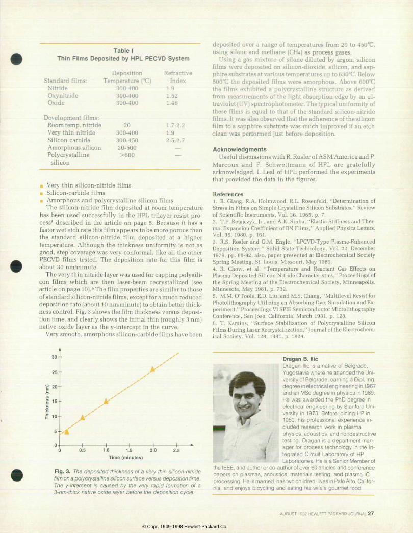
Table I Th in F i lms Deposi ted by HPL PECVD System
Standard films: Nitride Oxynitride Oxide
Deposition Temperature (°C)
300-400 300-400 300-400
Refractive Index
1.9 1.52 1.46
Very thin silicon-nitride films • Silicon-carbide films
Amorphous and polycrystalline silicon films The silicon-nitride film deposited at room temperature
has been used successfully in the HPL trilayer resist pro cess5 described in the article on page 5. Because it has a faster wet etch rate this film appears to be more porous than the standard silicon-nitride film deposited at a higher temperature. Although the thickness uniformity is not as good, step coverage was very conformal, like all the other PECVD films tested. The deposition rate for this film is about 30 nm/minute.
The very thin nitride layer was used for capping polysili- con films which are then laser-beam recrystallized (see article on page 10). 6 The film properties are similar to those of standard silicon-nitride films, except for a much reduced deposition rate (about 10 nm/minute) to obtain better thick ness control. Fig. 3 shows the film thickness versus deposi tion time, and clearly shows the initial thin (roughly 3 nm) native oxide layer as the y-intercept in the curve.
Very smooth, amorphous silicon-carbide films have been
0 . 5 1 . 0 1 . 5 2 . 0 Time (minutes)
2.5
Fig. 3 . The deposi ted th ickness of a very th in s i l icon-n i t r ide film time. a polycrystalline silicon surface versus deposition time. The y - i n te rcep t i s caused by the ve ry rap id fo rma t ion o f a 3-nm-th ick nat ive ox ide layer before the deposi t ion cyc le.
deposited over a range of temperatures from 20 to 450^. using silane and methane (CH») as process gases.
Using a gas mixture of silane diluted by argon, silicon films were deposited on silicon-dioxide, silicon, and sap phire substrates at various temperatures up to 630°C. Below 500°C the deposited films were amorphous. Above 600CC the films exhibited a polycrystalline structure as derived from measurements of the light absorption edge by an ul traviolet (UV) spectrophotometer. The typical uniformity of these films is equal to that of the standard silicon-nitride films. It was also observed that the adherence of the silicon film to a sapphire substrate was much improved if an etch clean was performed just before deposition.
Acknowledgments Useful discussions with R. Rosier of ASM/ America and P.
Marcoux and F. Schwettmann of HPL are gratefully acknowledged. I. Leal of HPL performed the experiments that provided the data in the figures.
References 1. R. of R.A. Holmwood, R.L. Rosenfeld, "Determinat ion of Stress in Films on Simple Crystalline Silicon Substrates," Review of Scientific Instruments, Vol. 36, 1965, p. 7. 2. T.F. Retajczyk, Jr., and A.K. Sinha, "Elastic Stiffness and Ther mal Expansion Coefficient of BN Films," Applied Physics Letters, Vol. 36, 1980, p. 161. 3. R.S. Rosier and G.M. Engle, "LPCVD-Type Plasma-Enhanced Deposition System," Solid State Technology, Vol. 22, December 1979, Society 88-92, also, paper presented at Electrochemical Society Spring Meeting, St. Louis, Missouri, May 1980. 4. R. Chow, et a l , "Temperature and Reactant Gas Effects on P lasma o f S i l i con Ni t r ide Charac te r i s t i c s , " P roceed ings o f the Spring Meeting of the Electrochemical Society, Minneapolis, Minnesota, May 1981, p. 732. 5. M.M. O'Toole, E.D. Liu, and M.S. Chang, "Multilevel Resist for Photolithography Utilizing an Absorbing Dye: Simulation and Ex periment," Proceedings VI SPIE Semiconductor Microlithography Conference, San Jose, California, March 1981, p. 128. 6. T. Kamins, "Surface Stabilization of Polycrystalline Silicon Films During Laser Recrystallization," Journal of the Electrochem ical Society, Vol. 128, 1981, p. 1824.
Dragan B. l l ic Dragan l l ic ¡s a native of Belgrade, Yugoslavia where he at tended the Uni versity of Belgrade, earning a Dipl. Ing. degree in electrical engineering in 1967 and an MSc degree in physics in 1969. He was awarded the PhD degree in e lect r ica l engineer ing by Stanford Uni versi ty in 1973. Before jo in ing HP in 1980, h is pro fess iona l exper ience in c luded research work in p lasma physics, acoust ics, and nondestruct ive tes t ing . Dragan i s a depar tment man ager fo r p rocess techno logy in the In tegrated Circui t Laboratory of HP Laboratories. He is a Senior Member of
the IEEE, and author or co-author of over 60 art icles and conference papers on p lasmas, acoust ics, mater ia ls test ing, and p lasma 1C processing. He is married, has two children, l ives in Palo Alto, Califor n ia , and en joys b icyc l ing and eat ing h is wi fe 's gourmet food.
AUGUST 1982 HEWLETT-PACKARD JOURNAL 27
© Copr. 1949-1998 Hewlett-Packard Co.
Electromigration: An Overview The l i fet ime of the very thin and narrow conductors used in VLSI circuits is largely determined by the operat ing current dens i ty and meta l l ic composi t ion. The pred ic ted l i fe t imes for var ious a l loys are d iscussed.
by Pau l P . Merchant
THE SHRINKAGE OF 1C DIMENSIONS places in creased loads on the current-carrying capability of metallization systems. At large current densities
electromigration damage can be a major reliability problem because this current-induced metal migration can lead to open-circuit failures in interconnect lines. Because elec tromigration resistance is a material-dependent property, the type of metallization system used in a particular 1C depends on interactions between processing, design and reliability considerations.
Although electromigration phenomena in bulk metals have been studied since the early part of this century, only in the past 15 years has attention been focused on thin polycrystalline metal films used for 1C conductors.1 Trans mission electron microscopy, radioactive tracer techniques and marker motion experiments have demonstrated that electromigration occurs because of a current-induced mi gration of metal atoms along a conductor. Models of the phenomenon begin with a calculation of the average force on a metal atom as the vector sum of an electrostatic force on a screened ion and a carrier "wind" effect resulting from carrier-atom scattering. In aluminum alloys the scattering term dominates and material transport proceeds from cathode to anode as shown in Fig. 1. Under conditions typically encountered in 1C metallization systems (103 to
106 A/cm2 current densities and temperatures much less than the melting temperature of the conductor) most metal atoms migrate along grain boundaries. If inhomogeneities exist in the conductor, arising for example from tempera ture gradients or grain-size divergences along the conduc tor, then the current-induced atom flow is nonuniform and material pile-up and voids occur in the conductor. As the current stressing continues, voids can coalesce to form cracks. This creates smaller cross-sectional areas of the conductor and thus leads to higher local current densities that accelerate the process. Eventually the cross-sectional area becomes so small that the conducting region melts and electrical continuity is lost. Regardless of whether the atom acted on by the current is a lattice atom neighboring a vacancy, or an interstitial or a solute impurity, this model predicts the same behavior for the time to failure (tf):1
tf = exp (Ea/kT)
where I is the current, A is the cross-sectional area of the conductor, Ea is an activation energy (typically close to that of grain-boundary diffusion) and T is the absolute tempera ture. B is a material-dependent proportionality constant which is a lumped parameter containing effects of other
Electron Scatter ing Force
T
T
Void Format ion
Crack Propagat ion
Continuity Fai lure
F i g . 1 . E l e c t r o m i g r a t i o n m e c h a n i s m s h o w i n g a n i d e a l i z e d c o n ductor (upper le f t ) wi th d i rect ions o f e lec t ron f l ux JE , e lec t ros ta t i c force eE and resul tant atomic f lux JA. Scanning electron microscope p h o t o g r a p h ( l o w e r l e f t ) o f v o i d fo rmat ion to the le f t o f the b reak a n d a c c u m u l a t i o n o f m a t e r i a l i n the form of hillocks to the right. The right half of this f igure outl ines the fai lure process.
2 8 H E W L E T T - P A C K A R D J O U R N A L A U G U S T 1 9 8 2
© Copr. 1949-1998 Hewlett-Packard Co.

Med ian T ime to Fa i l u re ( yea rs )
1 2 5 1 0 2 0 5 0 1 0 0 2 0 0 5 0 0 1 0 0 0 2 0 0 0 100.0
1 0 - 5 1 0 4 1 0 5 1 0 6 1 0 7
Median Time to Fai lure (hours)
parameters not explicitly included in the model. The parameter n depends on the type of inhomogeneity respon sible for atom flux divergences. For example, n = 3 for tem perature gradients and n = l for diffusion barriers or grain- size divergences. Typically, measured values for n are in the range of 2 to 3. Thus tf is very sensitive to linewidth, which is the principal problem when metallization dimen sions are scaled down.
While the more classical diffusion experiments are used in modeling electromigration, most reliability data in the semiconductor industry is obtained from accelerated life testing. A group of about 15 to 20 similar conductors is subjected to constant-current stressing at an elevated tem perature and the failure time of each conductor link is re corded. Usually the failure distribution is log-normal and is characterized by a median time to failure t50 (at which 50% of the lines have failed) and a parameter cr=log (t50/t16) that characterizes the spread of the distribution. When tests are done at several temperatures, with care taken to include corrections for joule heating at large current densities, Ar- rhenius plots of t50 versus link temperature yield the activa tion energy Ea. Testing at a fixed temperature, using various current densities, yields the exponent n. If tests are done using and with different grain structures, geometries, and substrate conditions, an empirical expression for B can be obtained. The scaling parameters Ea, n, and B are then used to predict the failure distribution for a similar group of conductors under normal operating conditions. Given the constraints of desired reliability, this data allows an 1C designer to set design rules for metallization systems with a fair degree of confidence. An example of design rule con straints for sputtered Al-Si(2%)-Cu(4%) metallization is given in Fig. 2.
Although gold is far superior to aluminum in its elec tromigration resistance, it is not compatible with silicon MOS devices. Aluminum, typically containing 1 to 2% silicon to prevent pitting of contact areas, is the industry standard for such devices. However, circuit dimensions have now reached the size where aluminum can no longer
Fig. 2 . Design ru les for sput tered AI-Si(2%)-Cu(4%) metal l izat ion al loyed at 450°C and operat ing at 90°C. The axes give median t ime t o f a / l u r e t 5 0 a n d c u r r e n t . C o n s tant -cur rent -dens i ty and conduc tor cross-sect ional -area contours a l l o w e a s y s e l e c t i o n o f d e s i r e d conductor s ize or current densi ty.
meet the reliability constraints placed on ICs. Several methods have been developed to extend the electromigra tion resistance of aluminum, such as passivating the surface of the metal with a hard dielectric overcoat or lightly dop ing the material with impurity metals. The coatings prevent material accumulation and cause stress-generated atom fluxes that oppose the current-driven atom flux, resulting in improvements in lifetime of about 10 times. Impurity dop ing with metals such as chromium, titanium, magnesium or copper tends to "plug up" the grain boundaries and can extend the lifetime of the metallization system by as much as 200 times with only about a 20% increase in the film's
10,000
0 . 5 1 2 5 1 0 2 0 3 0 5 0 7 0 8 0 9 0 9 5 9 8 9 9 . 5 Cumu la t i ve Fa i l u re (%)
F i g . 3 . A c c e l e r a t e d e l e c t r o m i g r a t i o n l i f e - t e s t p l o t s ( l o g - normal paper) of AI-Si(2%) al loys for di f ferent copper concen trat ions; (%) 0%, (m) 1%, and( l ) 4% Cu. Test done at 220°C and a current density of 106A/cm*. fso is found from the inter section of the 50% cumulative fai lure l ine and the straight- l ine f i t of the data points.
AUGUST 1982 HEWLETT-PACKARD JOURNAL 29
© Copr. 1949-1998 Hewlett-Packard Co.

resistivity. Copper is a common dopant in production pro cesses where wet chemical etching is used to pattern the metal. However, further development is still needed to ob tain a suitable dry etch process for narrow lines. At the present time, such development has generated considera ble interest in determining the effect of copper concentra tion of the electromigration resistance of aluminum alloys because dry etching processes can only successfully pattern aluminum films with less than 1% copper content. Com parative life-test data for sputtered Al-Si(2%) films having 0%, 1%, and 4% Cu added are shown in Fig. 3.
Another approach uses layered structures of aluminum with a transition element such as chromium or titanium, or with oxygen, which after heat treatment can form a hard layer within the metal that blocks crack propagation into neighboring layers.2 However, the intermetallic formation may in some cases (e.g., CrAl?) cause formation of voids and large and stresses that lead to increases in resistivity and lifting of narrow conductor lines.
Even more robust electromigration resistance can be ob tained by using refractory metals such as tungsten and molybdenum which are compatible with silicon 1C process ing and have fairly low resistivities and high melting tem peratures. The latter property results from a large activa tion energy for diffusion. Recent tests of sputtered tung sten films have yielded a t50 of 1200 hours under stress at a current density of 4 x 10⁶ A/cm2 and a link temperature of 415°C. (If the Al-Si(2%)-Cu(4%) film data is scaled to these stress conditions, the extrapolated t50 is only 1.7 hours.) Sputtered molybdenum films have also shown high electromigration resistance that is comparable to that of tungsten. However, the use of tungsten metallization does not allow a complete disregard of current-limit design rules, because at current densities of l.SxlO7 A/cm2 the same sputtered tungsten film glows yellow-white and fails
1 0 0 0 T
0.1
• 340 nm Oxide 34 nm Oxide Three 300-nm Oxide Steps
0 . 5 1 2 5 1 0 2 0 3 0 5 0 7 0 8 0 9 0 9 5 Cumulat ive Fai lure (%)
9 9
F ig . 4 . Acce le ra ted e lec t rom ig ra t i on l i f e - t es t p l o t s o f spu t tered Al-Si (2%) 2- turn2 conductors, TOO im long. The stress cond i t ions are a cur ren t dens i ty o f 1 x?o6 A/cm2 and a tem perature of 220°C. The different underlying substrate surfaces are (9) 34-nm-thick planar S/Oz, (- ) 340-nm-thick planar SiOz and (1 ) the same sur face as (m) w i th th ree ver t i ca l -wa l led , 300-nm-high S/Oz sfeps.
in less than 10 minutes as a result of severe self-heating effects.
Electromigration resistance is also affected by several processing and design parameters. Steps in the underlying topography can result in losses of cross-sectional area in metal lines. Either poor step coverage during metal deposi tion or a loss of linewidth control during subsequent photomasking can lead to early failures at step edges. Pro cessing goals should include gradual wall slopes and minimum step heights. Circuit layout should strive to minimize metal crossovers at severe steps. Planarization before metal deposition is desirable to prevent these effects. A tradeoff to be considered, however, is that as the underly ing insulator thickness is increased, the thermal sinking to the silicon substrate decreases, which leads to earlier fail ures as a result of the higher link temperature. Accelerated life-test plots illustrating these effects are shown in Fig. 4. If a diffusion barrier is not used, impurity dopants in the metal may also be driven into the substrate. This can result in semiconductor junction poisoning. Another design con sideration is the duty cycle, because between pulses, film stresses tend to relax electromigration effects. Obviously, symmetrical ac conditions are desirable for maximizing the lifetime of a given metallization system.
The final choice of a metallization system for a particular type of 1C depends on interactions between several con straints imposed by processing ease, and compatibility, circuit design, layout and reliability requirements. Accu rate can of a metallization system's reliability can only be made from accelerated test data on realistic simula tions of target vehicles. To achieve this goal it is important that all persons involved in processing and design be aware of the effects of their decisions on the reliability of the finished product.
Acknowledgments The test structures used in evaluating the electromigra
tion properties of candidate metallization systems are the result of the combined efforts of several persons in HP's 1C
Paul P . Merchant Paul Merchant was born in Bur l ington, Vermont, and attended the University of Vermont for a BS degree in phys ics (1972) and Brown Univers i ty for the ScM (1974) and PhD (1978) degrees, a lso in phys ics . He d id postdoctora l work in photoelectrolysis at Brown Uni versi ty for one year and in stoichiomet- r ic laser materials at Centre Nat' l de la Recherche Scient i f ique, Bordeaux, France, for one year. Paul then joined HP in 1 979 and has done R&D work related to e lect romigrat ion, dry etch ing, and suicide contacts and interconnects. His contr ibut ions have resul ted in several
papers on I I -VI compounds, t ransi t ion metal oxides, and laser mate rials. He is a memberof the American Physical Society, Sigma Xi, and the American Vacuum Society, and has taught c lasses on 1C metal l i zation technology. Paul is married, l ives in Menlo Park, California, and enjoys p lay ing Sof tbal l , racquetbal l , chess, keyboards, and gui tar .
3 0 H E W L E T T - P A C K A R D J O U R N A L A U G U S T 1 9 8 2
© Copr. 1949-1998 Hewlett-Packard Co.
Processing Lab (ICPL) for standard processing and Inte grated Circuits Lab (ICL) for unit processes currently under development. In particular. Joyce Sum of ICPL has provided the bulk of the metal depositions necessary for these studies. Assistance in testing and sample preparation and in metal film structural analysis was provided by Gladys Koke and Tom Cass, respectively, of ICL. The Systems Technology Operation at HP's Fort Collins. Colorado divi sion kindly supplied the sputtered tungsten films.
References 1 . P.M. D'Heurle and P.S. Ho. "Electromigration in Thin Films." in Thin FiJms Interdi/fusión 6- Reactions, edited by J.M. Poate, K.N. Tu and J.\V. Mayer. John Wiley and Sons. New York 1978, pp. 243-304. 2. J.K. Howard. J.F. White, and P.S. Ho. Journal of Applied Physics. Vol. 49. N!o. 7, 1978, p. 4083.
SWAMI: A Zero-Encroachment Local Oxidat ion Process Lateral oxidat ion l imits densi ty in oxide- isolated VLSI c i rcu i ts . This process removes th is l imi t by us ing a novel sequence of convent iona l process ing techn iques.
by Kuang Yi Chiu
AS DEVICE DIMENSIONS continue to shrink in the drive toward productivity and performance im provements, processing technology improvements
will be of major importance in achieving these goals. Elec tron beam and X-ray lithography, dry etching, and ion im plantation processes make it possible to fabricate devices with compatible interdependent requirements for image resolution, edge definition, step coverage, and functional ity at geometries at or below the one-micrometer level. However, the limits of certain aspects of the technology still exist. Device isolation is one of the major issues to consider for achieving high device packing density for VLSI. Local oxidation of silicon (LOCOS)1 has been widely used for the isolation of active components of silicon LSI circuits be cause it offers several advantages over other isolation tech nologies, such as surface planarity, improvement in pack ing density, and compatibility with existing LSI processing techniques. However, reducing LOCOS device dimensions for VLSI aplications is limited by severe encroachment re sulting from the lateral oxidation, or bird's beak (see Fig. 1), under the edge of the isolation mask and diffusion of the channel-stop doping into the active device area.
The channel narrowing resulting from the LOCOS pro cess, approximately two to three times the field oxide thickness, has been small enough that it has only a small effect at minimum widths of 4 to 5 /xm and is almost un- noticeable for channel widths greater than 5 /JLTTÃ. When devices are scaled down to micrometer and submicrometer levels, the field oxide has to scale down in thickness to control the lateral encroachment to an amount reasonable for dense layout ground rules. However, because of the
S W A M I L O C O S N i t r i d e I ( 1 5 0 n m ) - , S i 0 2 ( 4 5 n m )
(f)
F i g . 1 . C o m p a r i s o n o f S W A M I p r o c e s s w i t h c o n v e n t i o n a l LOCOS process, (a) Af ter is land pat tern ing and etch ing, (b) A f t e r I I I I d e p o s i t i o n ( S W A M I o n l y ) , ( c ) A f t e r n i t r i d e I I etching (SWAMI only), (d) After f ield oxidation, (e) After nitr ide removal and LPCVD oxide refi l l step (SWAMI only), (f) Finished isolat ion structure before gate oxidat ion.
AUGUST 1982 HEWLETT-PACKARD JOURNAL 31
© Copr. 1949-1998 Hewlett-Packard Co.
Table I SWAMI Process (see F ig . 1 )
Grow stress-relief oxide (SROI) Deposit silicon nitride (nitride I) Pattern island region (masking) Plasma etch SisN4 and SÃÃœ2 Plasma etch silicon step Grow stress-relief oxide (SROII) Deposit silicon nitride (nitride II) Plasma etch nitride II
9. Grow isolation field oxide 10. Strip nitride (wet etch) 11. Deposit and densify LPCVD SiCh 12. Etch back SiO2
reduced field oxide thickness, the interconnect capacitance increases proportionately and VLSI circuit performance is degraded. Experiments have been reported in which this undesirable feature caused by the LOCOS approach is minimized. However, either the bird's beak still exists (to a reduced degree) or the approach requires the use of com plex or unconventional processing techniques.
A side-wall-masked isolation (SWAMI) process using anisotropic plasma etching of silicon and silicon nitride/ oxide was developed to form a zero-encroachment and fully recessed isolation structure. The SWAMI process almost completely eliminates the reduction in effective channel width from defined mask dimensions. The process uses only conventional LSI processing techniques and no addi tional masking step is required. Table I outlines the se quence of steps in the fabrication process to form the isola tion structure. The process is similar to the conventional fully recessed oxidation process except that steps 6, 7, 8, 11, and 12 are needed to form this encroachment-free isolation scheme. Fig. 1 illustrates schematically the major process-
Fig. 2. Microphotograph of (a) SWAM! st ructure compared to (b) LOCOS st ructure before gate ox idat ion.
ing steps that deviate from the conventional LOCOS ap proach. The stress-relief oxide is thermally grown at 1000°C in a dry ambient followed by nitrogen annealing for 20 minutes. The silicon-nitride films are low-pressure chemical-vapor deposited (LPCVD) at 800°C in a 4: 1 volume ratio of NHsiSiFkCh. Positive photoresist and direct-step- on-wafer (DSW) projection were used throughout this study for pattern definition. The nitride and oxide are etched by C2p6 plasma2 and the silicon step is etched by CC14/C2F6 plasma.3 A boron channel-stop implant is performed after the silicon step etching. A second stress-relief oxide is grown and the nitride II layer is then deposited.
A strongly unidirectional plasma nitride etch is then used to remove the nitride II lying on the planar surface such that the edge of the island is covered by nitride II and the top island surface is protected by nitride I. The field oxide is then grown in a wet environment and the nitride films are stripped in boiling phosphoric acid. A layer of 500-nm-thick LPCVD oxide is deposited and etched back by plasma oxide etching such that a thin layer, approximately 50 nm thick, of oxide is left on the gate region. A short, wet oxide etch is then performed to remove the remaining thin oxide to prevent possible contamination of the gate region by the plasma and to avoid reformation of the notch at the edge of the silicon island. A comparison of conventional LOCOS and SWAMI isolation structures before gate oxida tion is illustrated in Fig. 2.
Experimental results and detailed analysis of MOSFET devices fabricated using this newly developed SWAMI process have been presented in other publications.4'5
References 1. J.A. Appels, etal, "Local oxidation of silicon and its application in semiconductor device technology," Phillips Research Reports, Vol. 25, no. 2, 1970, pp. 118-132. 2. G. Rankin, private communication. 3. M. Ben-Dor, private communication. 4. K.Y. Chiu, J. Moll, and J. Manoliu, "A Bird's-Beak Free Local Oxidation Technology Feasible for VLSI Circuits Fabrication," Special Joint Issue on VLSI of the IEEE Transactions on Electron Devices and IEEE Journal of Solid-State Circuits, April 1982. 5. T. lizuka, K.Y. Chiu, and J. Moll, "Double Threshold MOSFETs in a Bird's-Beak Free Structure," Proceedings of the IEEE Interna tional Electron Devices Meeting, paper no. 16.3, 1981.
Kuang Yi Chiu Kuang Chiu was born ¡n Taiwan and educated at the University of Sourthern Cal i fornia where he received a PhD de gree in mater ia l sc ience in 1974. He joined HP in 1979 with six years experi ence related to InSb infrared sensor ar rays and rad ia t ion ef fects on MOS de v ices. Kuang is current ly work ing on MOS/VLSI process development. He is a co-author of nine articles related to the areas he has worked in and is a member of the IEEE. Kuang enjoys f ish ing , camping, p lay ing br idge, and sports. He l ives in Palo Alto, California, is marr ied, and has a son and a daugh ter.
3 2 H E W L E T T - P A C K A R D J O U R N A L A U G U S T 1 9 8 2
© Copr. 1949-1998 Hewlett-Packard Co.

Trench Isolation Technology
I n r ecen t yea rs , t he re has been i nc reas ing i n te res t i n com p lementary meta l -ox ide-semiconductor (CMOS) techno logy fo r i t s l ow power d i ss ipa t ion , l a rge opera t ing vo l tage marg in and supe r io r no i se immun i t y . As the dens i t y o f i n teg ra ted c i r cu i t s con t i nues t o g row , t he power d i ss i pa t i on advan tage makes i t c lear that CMOS wil l be a major VLSI technology. However, there is one factor working against CMOS in scal ing device dimensions down, the la tch-up prob lem.
Fig. the il lustrates the cross section of a CMOS inverter with the two- t rans is to r (pnp and npn) equ iva len t c i r cu i t super imposed . Latch-up can be created in the parasit ic pnpn path by the posit ive feedback between two coup led b ipo lar t rans is tors , produc ing a regenerat ive swi tch ing and a l lowing large cur rents to f low. Cer t a i n i s s p a c i n g b e t w e e n n - a n d p - c h a n n e l t r a n s i s t o r s i s required to prevent th is la tch-up. Therefore, the spacing cannot be reduced as much as the t rans is tor d imensions.
The trench isolat ion technology provides a possible solut ion to this scal ing problem. As shown in Fig. 2, when a deep and narrow trench is etched into the si l icon substrate and ref i l led with dielec t r i c m a t e r i a l , t h e s p a c i n g b e t w e e n t w o t r a n s i s t o r s c a n b e minimized wi thout increasing the potent ia l for la tch-up.
B e s i d e s t h e C M O S l a t c h - u p p r e v e n t i o n , d i e l e c t r i c r e f i l l e d t renches can also be used for general device isolat ion in bipolar and MOS in tegrated c i rcu i ts .
For circuit density, the trenches need to be as narrow as possi ble. The current optical l i thography technology l imits their width to no less than 1 /¿m. The trench depth is approximately 5 to 8 /um, depend ing upon dev ice s t ruc tures and dop ing pro f i les .
To form such deep and narrow t renches, the e tch ing must be h i g h l y u n f o r m i n g v e r t i c a l s i d e w a l l s w i t h n o l a t e r a l u n dercuts . Th is character is t ic has been demonst ra ted by react ive ion e tch ing . The c ross sec t ion o f a re f i l led t rench taken w i th a scanning electron microscope (SEM) is shown in Fig. 3. The ref i l l technique depends upon two processes: conformal coat ing and e tch ing back an iso t rop ica l l y . The low-pressure chemica l -vapor deposit ion of the dielectr ic material results ¡n equivalent deposi t i o n r a t e s o n t h e t r e n c h s i d e w a l l s a n d t h e s i l i c o n s u r f a c e . Trenches 1 /xm wide can be sealed with a 0.5-/¿m-thick deposi t i on . The depos i t i on i s f o l l owed by an an i so t rop i c e t ch o f t he sur face-deposi ted layer . Thus, a reasonably p lanar sur face can be obta ined as shown by the SEM v iew.
VIN
n-Well p-Substrate
F ig . 1 . C ross sec t i on o f CMOS inve r te r s t r uc tu re w i t h t he two-transistor equivalent circuit superimposed. This transistor combination can act as a lateral SCR structure that wil l turn on when large cur rents are passed, i f the spac ing between the transistors is smal l enough to permit regenerat ive feedback.
P+ P +
n-Well
Trench-»-
Latch-Up Path
p-Substrate
Fig. 2. By etching a deep trench between the two transistors ¡n Fig. 1 and refi l l ing the trench with a dielectric material, the t rans is to rs can be spaced c loser toge ther , bu t the pa th fo r regenerat ive feedback wi l l st i l l remain long enough to prevent latch-up.
Poten t i a l p rob lems tha t may be i n t roduced by t renches a re t rench can i nve rs ion and su r face topography . The fo rmer can cause MOS transistors to be leaky or to short through the inversion path. The lat ter can cause a nonplanar surface on the top of the re f i l led t rench, c reat ing the potent ia l p rob lem of b reaks in any conduct ive l ines that run across the t rench.
Some MOS transistors surrounded by t renches have been suc cessful ly fabr icated. These devices have electr ical behavior very simi lar to devices without t renches, showing no residual leakage currents above the 1 -pA range. The yield was also about the same as for the nontrench devices after a large number of devices were tested.
-Shang-y i Chiang
Fig. 3. Cross-sect ional microphotograph of a ref i l led t rench.
AUGUST 1982 HEWLETT-PACKARD JOURNAL 33
© Copr. 1949-1998 Hewlett-Packard Co.
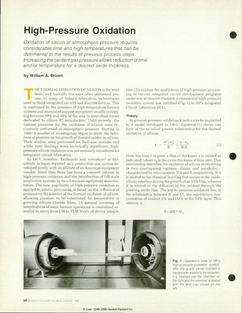
High-Pressure Oxidation Oxidat ion of s i l icon at a tmospher ic pressure requi res cons iderab le t ime and h igh tempera tures tha t can be detr imenta l to the resul ts of prev ious process s teps. Increasing the oxidant gas pressure al lows reduction of t ime and /or temperature for a desi red oxide th ickness.
by Wi l l iam A. Brown
THE THERMAL OXIDATION OF SILICON is the most basic, and typically the most often performed pro cess in many of today's fabrication technologies
used to build integrated circuits and discrete devices. This is confirmed by the presence of high-temperature furnace systems and associated support equipment usually occupy ing between 30% and 40% of the area in most clean rooms dedicated to silicon 1C manufacture. Until recently, the various processes for the oxidation of silicon were ex clusively performed at atmospheric pressure. Starting in I9601 a number of investigators began to study the influ ence of pressure on the growth of thermal oxides on silicon. Their studies were performed on R&D-size systems and while their findings were technically significant, high- pressure silicon oxidation was not seriously considered for integrated circuit fabrication.
In 1977, however, Tsubouchi and coworkers2 at Mit subishi in Japan reported on a production-size system de veloped jointly with an affiliate of an American equipment vendor. Since then there has been a renewed interest in high-pressure oxidation and the introduction of full-scale production systems by two American equipment manufac turers. The new popularity of high-pressure oxidation as applied to silicon processing is based on the influence of pressure on the kinetics of the thermal oxidation of silicon, allowing pressure to be substituted for temperature in growing silicon-dioxide films. (A general lowering of temperatures of most furnace operations is considered es sential to move from LSI to VLSI levels of device integra
tion.) To explore the application of high-pressure process ing to various integrated circuit development programs under way at Hewlett-Packard, a commercial high-pressure oxidation system was installed (Fig. 1) in HP's Integrated Circuit Laboratory (ICL).
Theory In general, pressure oxidation kinetics can be explained
by a model developed in 1965. 3 Equation (I) shows one form of the so-called general relationship for the thermal oxidation of silicon.
(1) B/A
Here, the time t to grow a film of thickness x is related as indicated, where x0 is the oxide thickness at time zero. This relationship describes the oxidation of silicon as occurring in two overlapping regimes — linear and parabolic — characterized by rate constants B/A and B, respectively. B/A is related to the chemical bonding that occurs at the oxide- silicon interface during the growth of an SiU2 film, whereas B is related to the diffusion of the oxidant through the growing oxide film. The key to pressure oxidation lies in the relationship between B and C*, the equilibrium con centration of oxidant (Oi and H2Ãœ) in the SÃÃœ2 layer. This relation is
B=2DC*/N¡
•*•
F i g . 1 . O p e r a t o r ' s v i e w o f H P ' s h igh -p ressu re ox ida t i on sys tem. After the quartz carr ier (center) is loaded with wafers to be oxidized, i t is inser ted in to the chamber on the right and the chamber is sealed w i t h t h e e n d c a p s h o w n o n t h e left.
3 4 H E W L E T T - P A C K A R D J O U R N A L A U G U S T 1 9 8 2
© Copr. 1949-1998 Hewlett-Packard Co.

where D is the diffusivity of the oxidant and N¡ is the number of oxidant molecules per unit volume of the oxide. C is directly proportional to the partial pressure pox of the oxidant in the surrounding ambient atmosphere: there fore as pox increases, so does C*.
An example of the effect of steam pressure on the parabolic rate constant B is shown in Fig. 2. It is seen that B can increase by 5 to 10 times its value at atmospheric pres sure, given a very moderate increase in the pressure of the oxidation ambient gases. As shown in Fig. 3, B/ A is likewise influenced by pressure. At 900°C, for example, B/A in creases by a factor of 20 when the pressure is increased from 1 atmosphere (1.033 kg/cm2) to 15 kg/cm2.
Applications What does high-pressure oxidation offer for integrated
circuit fabrication? Some features of this technology are itemized in Table I. An acceleration in the growth rate of the thermal oxide film provides the process designer two op tions. First, one can retain the temperature and time of an existing atmospheric-pressure process and take advantage of the enhanced growth rate associated with high pressure. It has been observed that, compared to atmospheric-oxida tion conditions, the growth rate at an elevated pressure P increases nearly linearly with P. Second, one may choose to lower the temperature of an existing oxidation process by performing it at elevated pressure while retaining the atmospheric pressure growth rate so as not to impact the throughput of a given operation. Typically, for every one-
4 - -
5 1 0
Steam Pressure (kg/cm2)
15
Fig. 2. Effect of steam pressure on the parabolic rate constant B for <100> s i l i con sur face or ienta t ion.
Table I Features of High-Pressure Oxidat ion
1. Accelerated oxidations 2. Low-temperature processing:
Less warping of large-diameter wafers Less effect on pn junction location
Xj (vertical and lateral) Fewer oxidation-induced stacking faults4 Denser oxides (higher refractive index) Reduced dopant segregation at the Si/SiCh interface
3. Offers a new dimension in silicon processing
atmosphere increase in pressure it is possible to lower the oxidation temperature by up to 30°C without changing an established oxidation. It is this latter option that has prompted the current interest in high-pressure oxidation.
Low-temperature oxidations provide the benefits out lined in item 2 of Table I. Of particular significance to circuit yields has been the reduction in various oxidation- induced stresses and structural defects in the underlying silicon that has been observed as a result of high-pressure oxidation.4 As device densities and chip size increase to ward VLSI levels of integration, structural perfection will be required of both the oxide and the silicon. Lastly, adding a third dimension to the oxidation process will permit the development of new device structures in the future.
Equipment The high-pressure oxidation system in HP's Integrated
Circuit Laboratory (Fig. 1) is capable of establishing operat ing pressures up to 25 atmospheres in a variety of ambients. For oxidation, either dry oxygen or water-injected steam environments may be established at any temperature be tween 500 and 1000°C. The system uses a quartz paddle for wafer t ransport (shown supported by an elevator mechanism in Fig. 1) attached to a quartz end cap inside a movable sealing door. Wafer oxidation takes place inside a quartz tube that resides within a heating element that is enclosed within a water-cooled pressure vessel. During processing the pressure in the quartz tube is always positive with respect to the vessel (to minimize wafer contamina tion) and gases continuously flow through both vessel and tube. A microcomputer is dedicated for control of all pro cess parameters as well as operation sequencing. Safety of operation is assured through hardwired alarms that can automatically abort a process and return the system to at mospheric pressure. The pressure vessel is outfitted with rupture discs to relieve any unintended overpressurization. The system is capable of processing up to 250 75- or 100- mm-diameter wafers.
Status In the last few years an increasing number of reports
dealing with various aspects of high-pressure silicon oxida tion have appeared in the technical literature. At present sufficient data on high-pressure oxides has been developed to permit their use at most of the oxide growth steps found in a typical integrated circuit process. In addition, some
AUGUST 1982 HEWLETT-PACKARD JOURNAL 35
© Copr. 1949-1998 Hewlett-Packard Co.

10
0.1- -
1200°C 1100°C 1000°C 900°C H 1 1 -t— I-
8 9
( 1 / T ) x 1 0 > ( K - 1 )
800°C 1
10
Fig. 3 . Ef fect o f temperature and pressure on the l inear ra te c o n s t a n t B / A f o r < 1 1 1 > a n d < 1 0 0 > s i l i c o n s u r f a c e o r i e n t a tions.
investigators have observed improved device performance when atmospheric-pressure-grown oxides are replaced by films grown in a high-pressure oxidation system. Several domestic semiconductor companies are already using a high-pressure oxide growth operation as the basis for their oxide-isolated bipolar 1C products.
At ICL the focus of current work is aimed at improve ments in device structures and density that can be realized by accelerated oxidations. Research into other applications of high-pressure silicon processing , such as implant activa tion, electronic charge neutralization, and novel film form ing processes, is being planned. It is clear that high- pressure oxidation will play a critical role in future inte grated circuit processing technology.
A c k n o w l e d g m e n t s Several people have contributed to establishing a high-
pressure oxidation capability in Hewlett-Packard Labora tories. They are, in random order, Rick Dalla, Armando Iturralde, Dave Thrasher, Dan Cropper, Conrad Dell'Oca, Eileen Murray, Bob Grimm, Pat Castro, and Fred Schwett- mann. Their ideas and support are gratefully acknowl edged.
References 1. J.R. Ligenza, "Oxidation of Silicon by High-Pressure Steam," Journal of the Electrochemical Society, Vol. 109, no. 2, March 1962, p 73. 2. N. Tsubouchi, et al, "Oxidation of Silicon by High-Pressure Steam," Japanese Journal of Applied Physics, Vol. 16, no. 5, May 1977, p 1055. 3. B. Deal and A. Grove, "General Relationship for the Thermal Oxidation of Silicon," Journal of Applied Physics, Vol. 36, no. 12, December 1965, p 3770. 4 . N . Tsubouch i , H . Miyosh i , and H. Abe , "Suppress ion o f Oxidation-Induced Stacking Fault Formation in Silicon by High- Pressure Steam Oxidation," Japanese Journal of Applied Physics, Vol. 17, no. 2, February 1978, p 227.
Wil l iam A. Brown Bi l l Brown is a product ion process en g ineer a t HP's In tegrated Ci rcu i t D iv i sion, Santa Clara, Cali fornia. He joined HP in 1975 with several years of product and process engineering experience in the commercial 1C business. His work at HP and e lsewhere has focused on high-temperature 1C processing, result ing in several papers and two patents. Born in Remsen, New York, he attended N iagara Un ivers i ty , earn ing a BS de gree in chemist ry in 1958, and Rens- se laer Poly technic Univers i ty , earn ing a master 's degree in meta l lurg ica l engineering in 1961 . Bi l l isamemberof
the American Vacuum Society, has taught courses in si l icon 1C pro cessing at HP and a local college, and recently spent three months in Korea helping the Korean Institute of Electronic Technology set up an 1C fabrication facility. Bill l ives in San Jose, California, is married, has two ch i ldren, and is in terested in personal computers and youth motocross racing.
H e w l e t t - P a c k a r d C o m p a n y , 3 0 0 0 H a n o v e r Street , Palo Al to, Cal i fornia 94304
H E W L E T T - P A C K A R D J O U R N A L
AUGUST 1982 Volume 33 • Number 8 T e c h n i c a l I n f o r m a t i o n f r o m t h e L a b o r a t o r i e s o f
H e w l e t t - P a c k a r d C o m p a n y Hewle t t -Packard Company, 3000 Hanover St reet
Palo Al to. Cal i forn ia 94304 U.S A. Hewlet t -Packard Centra l Mai l ing Depar tment
Van Heuven Goedhar t laan 121 1181 KK Amste lveen. The Nether lands
Yokogawa-Hewle t t -Packard L td . , Sug inami -Ku Tokyo 168 Japan Hewlet t -Packard (Canada) Ltd
6877 Goreway Dr ive . Miss issauga, Ontar io L4V 1M8 Canada
Bulk Rate U.S. Postage
Paid Hewlett-Packard
Company
FPCADÃVES CENTÈ*
C H A N G E O F A D D R E S S : To change Send address or delete your name f rom our mai l ing l is t p lease send us your o ld address label . Send c h a n g e s A l l o w d a y s . J o u r n a l . 3 0 0 0 H a n o v e r S t r e e t , P a l o A l t o , C a l i f o r n i a 9 4 3 0 4 U . S . A . A l l o w 6 0 d a y s .
5953-8502
© Copr. 1949-1998 Hewlett-Packard Co.