1 synchronous finite state machines; design and...
TRANSCRIPT

Prof. Dr. J. Reichardt Prof. Dr. B. Schwarz
Digital Systems © B. Schwarz 1-1
university of applied sciences hamburg DEPARTEMENT OF ELECTRICAL ENGINEERING
AND COMPUTER SCIENCE
1 Synchronous Finite State Machines; Design and Behaviour
1.1 Models for FSMs
Mealy machine
Combinational logic expressions for the Mealy FSM: S+ = f (I, S) and O = fMealy(I, S)
I
Feedback of the present state
external inputs
Mealy-FSM Next State Forming Logic
State Register Output
Forming Logic
O
CLK
S+ S
I

Prof. Dr. J. Reichardt Prof. Dr. B. Schwarz
Digital Systems © B. Schwarz 1-2
university of applied sciences hamburg DEPARTEMENT OF ELECTRICAL ENGINEERING
AND COMPUTER SCIENCE
S
external inputs
Medvedev-FSMNext State Forming Logic
State Register
O
CLK
S+
I
Moore- and Medvedev FSM Combinational logic expres-sions: S+ = f (I, S) and O = fMoore( S) The output signals of a Medvedev FSM are driven by the state flipflops : S+ = f (I, S) and O = S
Feedback of the present state
external inputs
Moore-FSM Next State Forming Logic
State Register Output
Forming Logic
O
CLK
S+ S
I

Prof. Dr. J. Reichardt Prof. Dr. B. Schwarz
Digital Systems © B. Schwarz 1-3
university of applied sciences hamburg DEPARTEMENT OF ELECTRICAL ENGINEERING
AND COMPUTER SCIENCE
1.2 Design Steps 1. Derivation of a state transition- and output-table with mnemonics. A state diagram can be
chosen as a graphical alternative. Usually the given problem is written in text form or can be described by a timing diagram.
2. Reduction of redundant states in order to simplify the handling of the solution and save
hardware resources. 3. Selection of appropriate state signals with binary representation and assign it to the reduced
number of mnemonic state names: state encoding. 4. Choose a flip-flop type for the state register implementation (usually D-FF with S+ = Q+ = D). 5. Derivation of a state transition table with additional output signal columns. 6. Derivation of logic equations for the flip-flop inputs and the outputs by K-maps.
7. Analysis of critical FSM state transitions after the state register has entered unused states.
8. Derivation of a logic design from the logic equations.

Prof. Dr. J. Reichardt Prof. Dr. B. Schwarz
Digital Systems © B. Schwarz 1-4
university of applied sciences hamburg DEPARTEMENT OF ELECTRICAL ENGINEERING
AND COMPUTER SCIENCE
Example: Sequence Detector
Assuming a synchronised 2 bit input stream, one should design the circuit such that a 1 is output whenever the desired sequence is recognised: I = ...,01,11,10,...
The output bit O of the synchronous FSM should be 1 just for one clock cycle. The leading bit combination 01 may appear for more than one clock cycle.
• All design steps will be explained (except state reduction which is not necessary with this
example). We will examine the Moore and Mealy FSM implementations. • For both FSM models a synthezisable VHDL code will be presented. • The timing of state transitions, next state calculations and output generation is presented
by VHDL simulations with symbolic signal propagation delays.

Prof. Dr. J. Reichardt Prof. Dr. B. Schwarz
Digital Systems © B. Schwarz 1-5
university of applied sciences hamburg DEPARTEMENT OF ELECTRICAL ENGINEERING
AND COMPUTER SCIENCE
Moore FSM Meaning of states: • S0 : start_state, wait on I="01".
State will be entered after reset. • S1: read_01, wait on "11" • S2: read_11, wait on "10" • S3: read_10, sequence recognised,
output O='1' • In each state 4 input combinations of in-
put signal I have to be answered with a next state calculation: 4 arcs have to placed.
• To each state an output value is assigned.
read_01
read_10 read_11
start_state
reset
Prof. Dr. J. Reichardt Prof. Dr. B. Schwarz
Digital Systems © B. Schwarz 1-6
university of applied sciences hamburg DEPARTEMENT OF ELECTRICAL ENGINEERING
AND COMPUTER SCIENCE
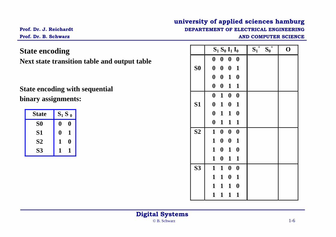
State encoding Next state transition table and output table State encoding with sequential binary assignments:
State S1 S 0 S0 S1 S2 S3
0 0 0 1 1 0 1 1
S1 S0 I1 I0 S1+ S0
+ O
S0 0 0 0 0 0 0 0 1 0 0 1 0 0 0 1 1
S1
0 1 0 0 0 1 0 1 0 1 1 0 0 1 1 1
S2 1 0 0 0 1 0 0 1 1 0 1 0 1 0 1 1
S3 1 1 0 0 1 1 0 1 1 1 1 0 1 1 1 1

Prof. Dr. J. Reichardt Prof. Dr. B. Schwarz
Digital Systems © B. Schwarz 1-7
university of applied sciences hamburg DEPARTEMENT OF ELECTRICAL ENGINEERING
AND COMPUTER SCIENCE
K-map representation for NS and output forming logic
S0+:
S0+= ...
S1+:
S1+= ...
O:
O= ...
Combinational logic expressions:

Prof. Dr. J. Reichardt Prof. Dr. B. Schwarz
Digital Systems © B. Schwarz 1-8
university of applied sciences hamburg DEPARTEMENT OF ELECTRICAL ENGINEERING
AND COMPUTER SCIENCE
VHDL code for the Moore FSM • Additional requirement: Execution of state transitions has to be controlled by an external enable in-
put signal ENABLE = '1' . • Straightforward approach: Separate the synchronous register from the combinational logic used for
computation of the next state and the output. FSM model is described by three processes. entity FSM_1_MOORE is port( CLK, RESET, ENABLE : in bit; -- secondary input signals I : in bit_vector(1 downto 0); -- input vector O : out bit ); -- output bit end FSM_1_MOORE; architecture SEQUENCE of FSM_1_MOORE is type STATES is (S0, S1, S2, S3); -- enumeration type signal STATE,NEXT_S: STATES ; -- process communication begin STATE_REGISTER: process(CLK, RESET) -- present state generation begin if RESET = '1' then STATE <= S0 after 20 ns; elsif CLK = '1' and CLK'event then -- positive edge controlled if ENABLE = '1' then STATE <= NEXT_S after 10 ns; -- synchronous control end if; end if; end process STATE_REGISTER; NS_D: process(I, STATE) -- next state forming logic for D-flip-flops begin

Prof. Dr. J. Reichardt Prof. Dr. B. Schwarz
Digital Systems © B. Schwarz 1-9
university of applied sciences hamburg DEPARTEMENT OF ELECTRICAL ENGINEERING
AND COMPUTER SCIENCE
case STATE is when S0 => if I = "01" then NEXT_S <= S1 after 20 ns; else NEXT_S <= S0 after 20 ns; end if; when S1 => if I = "11" then NEXT_S <= S2 after 20 ns; elsif I = "01" then NEXT_S <= S1 after 20 ns; else NEXT_S <= S0 after 20 ns; end if; when S2 => if I = "10" then NEXT_S <= S3 after 20 ns; elsif I = "01" then NEXT_S <= S1 after 20 ns; else NEXT_S <= S0 after 20 ns; end if; when S3 => if I = "01" then NEXT_S <= S1 after 20 ns; else NEXT_S <= S0 after 20 ns; end if; end case; end process NS_D; FSM_OUT: process(STATE) -- output forming logic of a Moore FSM begin
case STATE is when S3 => O <= '1' after 20 ns; when others => O <= '0' after 20 ns; end case; end process FSM_OUT; end SEQUENCE;

Prof. Dr. J. Reichardt Prof. Dr. B. Schwarz
Digital Systems © B. Schwarz 1-10
university of applied sciences hamburg DEPARTEMENT OF ELECTRICAL ENGINEERING
AND COMPUTER SCIENCE
Simulation results for the Moore FSM
Prof. Dr. J. Reichardt Prof. Dr. B. Schwarz
Digital Systems © B. Schwarz 1-11
university of applied sciences hamburg DEPARTEMENT OF ELECTRICAL ENGINEERING
AND COMPUTER SCIENCE
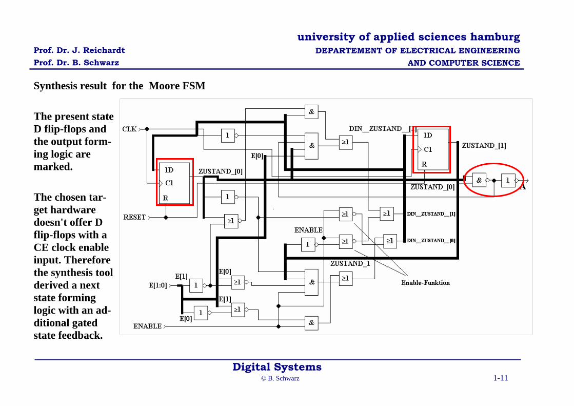
Synthesis result for the Moore FSM The present state D flip-flops and the output form-ing logic are marked. The chosen tar-get hardware doesn't offer D flip-flops with a CE clock enable input. Therefore the synthesis tool derived a next state forming logic with an ad-ditional gated state feedback.

Prof. Dr. J. Reichardt Prof. Dr. B. Schwarz
Digital Systems © B. Schwarz 1-12
university of applied sciences hamburg DEPARTEMENT OF ELECTRICAL ENGINEERING
AND COMPUTER SCIENCE
Sequence recognition by a Mealy FSM
The Mealy FSM implementa-tion uses only three states be-cause the output is under di-rect influence of the external input I. Therefore state S2 can supply both output levels.
We have to remember that the Mealy output reflects full asynchronous behaviour of external inputs.
I/O S
S1S0
S2
reset

Prof. Dr. J. Reichardt Prof. Dr. B. Schwarz
Digital Systems © B. Schwarz 1-13
university of applied sciences hamburg DEPARTEMENT OF ELECTRICAL ENGINEERING
AND COMPUTER SCIENCE
VHDL code for the Mealy FSM including a testbench entity TEST_B_1_ME is -- no external inputs end TEST_B_1_ME; architecture SEQUENCE of TEST_B_1_ME is signal CLK_I, RESET_I, ENABLE_I, O_I: bit; -- internal signals signal I_I: bit_vector(1 downto 0); type STATES is (S0, S1, S2); -- enumeration type signal STATE,NEXT_S: STATES ; begin STATE_REGISTER: process(CLK_I, RESET_I) -- present state flip-flops begin if RESET_I = '1' then STATE <= S0 after 20 ns; elsif CLK_I = '1' and CLK_I'event then if ENABLE_I = '1' then STATE <= NEXT_S after 20 ns; end if; end if; end process STATE_REGISTER; NS_D: process(I_I, STATE) -- next state forming logic begin
NEXT_S <= S0 after 20 ns; -- default assignment case STATE is when S0 => if I_I = "01" then NEXT_S <= S1 after 20 ns; end if;

Prof. Dr. J. Reichardt Prof. Dr. B. Schwarz
Digital Systems © B. Schwarz 1-14
university of applied sciences hamburg DEPARTEMENT OF ELECTRICAL ENGINEERING
AND COMPUTER SCIENCE
when S1 => if I_I = "11" then NEXT_S <= S2 after 20 ns; elsif I_I = "01" then NEXT_S <= S1 after 20 ns; end if; when S2 => if I_I = "01" then NEXT_S <= S1 after 20 ns; end if; when others => null; end case; end process NS_D; FSM_OUT: process(I_I, STATE) -- output under direct control of input begin I_I <= '0' after 20 ns; -- default assignment if (STATE = S2 and I_I = "10") then I_I <='1' after 20 ns; end if; end process FSM_OUT; --==================== testbench processes ================================== CLOCK: process -- clock cycle generator; not synthesizable begin CLK_I <= '0'; wait for 100 ns; CLK_I <= '1'; wait for 100 ns; end process CLOCK;

Prof. Dr. J. Reichardt Prof. Dr. B. Schwarz
Digital Systems © B. Schwarz 1-15
university of applied sciences hamburg DEPARTEMENT OF ELECTRICAL ENGINEERING
AND COMPUTER SCIENCE
STIMULUS: process -- stimulus sequence begin ENABLE_I <= '1'; RESET_I <= '1'; I_I <= "01"; wait for 270 ns; RESET_I <= '0'; wait for 100 ns; I_I <= "11"; wait for 200 ns; I_I <= "10"; wait for 40 ns; -- O_I <= '1' I_I <= "00"; wait for 60 ns; -- hazard in I I_I <= "10"; wait for 130 ns; -- O_I <= '1' I_I <= "01"; wait for 200 ns; ENABLE_I <= '0'; I_I <= "11"; wait for 200 ns; -- remain in S1 ENABLE_I <= '1'; wait for 100 ns; I_I <= "10"; wait for 250 ns; I_I <= "11"; wait for 200 ns; I_I <= "10"; wait for 250 ns;
-- wait; -- simulation stoped end process STIMULUS; end SEQUENCE;

Prof. Dr. J. Reichardt Prof. Dr. B. Schwarz
Digital Systems © B. Schwarz 1-16
university of applied sciences hamburg DEPARTEMENT OF ELECTRICAL ENGINEERING
AND COMPUTER SCIENCE
Simulation result for the Mealy FSM

Prof. Dr. J. Reichardt Prof. Dr. B. Schwarz
Digital Systems © B. Schwarz 1-17
university of applied sciences hamburg DEPARTEMENT OF ELECTRICAL ENGINEERING
AND COMPUTER SCIENCE
Synthesis results for the Mealy FSM The Mealy FSM im-plementation is smaller than the cor-responding Moore circuit. Synthesized expres-sions with ENABLE='1': Transformation with DeMorgan shows that the Mealy FSM out-put is erroneous if the state S = 11 is en-tered. A = ¬E(0) ∧ E(1) ∧ Z(1); Z(0)+ = ¬E(1) ∧ E(0); Z(1)+ = E(0) ∧ Z(0) ∧ ¬Z(1) ∧ {E(1) ∨ ¬E(0) }

Prof. Dr. J. Reichardt Prof. Dr. B. Schwarz
Digital Systems © B. Schwarz 1-18
university of applied sciences hamburg DEPARTEMENT OF ELECTRICAL ENGINEERING
AND COMPUTER SCIENCE
1.3 Recommended VHDL Coding Style
A reduced FSM model consists of only two blocks: • A synchronously clocked present state register. • The block C-Logic (combinational logic) con-
tains all the logic gates to derive the next state signals and the output signals.
• A direct coupling between the inputs I and the output O (red dotted arrow) characterises a Mealy FSM.
Correspondingly the FSM can be coded by two processes: One for the clocked process to update the state register and another combinational proc-ess for conditionally deriving the next machine state and to update the outputs. Medvedev FSMs can be described even with only one process.
Next
States
S +
States
S Present State
Register
Clock Reset Enable
C-Logic
Inputs
I O
Outputs

Prof. Dr. J. Reichardt Prof. Dr. B. Schwarz
Digital Systems © B. Schwarz 1-19
university of applied sciences hamburg DEPARTEMENT OF ELECTRICAL ENGINEERING
AND COMPUTER SCIENCE
Two process modelling of the Moore FSM for sequence recognition ( Timing is identical to results on p. 10)
-- FSM 2-processes: sequence detector (01,11,10) entity FSM_2p is port( CLK, RESET, ENABLE : in bit; I: in bit_vector(1 downto 0); O: out bit ); end FSM_2p; architecture SEQUENCE of FSM_2p is type STATES is (S0, S1, S2, S3); signal STATE,NEXT_S: STATES; begin REGISTER: process(CLK, RESET) -- present state D flip-flops begin if RESET = '1' then STATE <= S0 after 20 ns; elsif CLK = '1' and CLK'event then if ENABLE='1' then STATE <= NEXT_S after 20 ns; end if; end if; end process REGISTER;

Prof. Dr. J. Reichardt Prof. Dr. B. Schwarz
Digital Systems © B. Schwarz 1-20
university of applied sciences hamburg DEPARTEMENT OF ELECTRICAL ENGINEERING
AND COMPUTER SCIENCE
CL: process(I, STATE) -- combinational logic begin O <= '0' after 20 ns; NEXT_S <= S0 after 20 ns; -- default assignments case STATE is when S0 => if I = "01" then NEXT_S <= S1 after 20 ns; end if; when S1 => if I = "11" then NEXT_S <= S2 after 20 ns; elsif I = "01" then NEXT_S <= S1 after 20 ns; end if; when S2 => if I = "10" then NEXT_S <= S3 after 20 ns; elsif I = "01" then NEXT_S <= S1 after 20 ns; end if; when S3 => O <= '1'; -- Moore behaviour if I = "01" then NEXT_S <= S1 after 20 ns; end if; end case; end process CL; end SEQUENCE;

Prof. Dr. J. Reichardt Prof. Dr. B. Schwarz
Digital Systems © B. Schwarz 1-21
university of applied sciences hamburg DEPARTEMENT OF ELECTRICAL ENGINEERING
AND COMPUTER SCIENCE
1.4 Decoupling of FSMs
• The upper limit of the clock frequency which can be applied to a synchronous digital sys-tem is determined by the maximum signal delay through the combinational logic between two flip-flops (critical path).
• With coupled FSMs in large designs long combinational logic path may result. Namely the
output forming logic of a preceding FSM can be connected to the next state forming logic of a following FSM!
• Furthermore we have to be aware that Mealy FSMs which are coupled in a feedback loop may cause a so called combinational loop which will result in an oscillating circuit or will yield unwanted memory effects.
Combinational Logic

Prof. Dr. J. Reichardt Prof. Dr. B. Schwarz
Digital Systems © B. Schwarz 1-22
university of applied sciences hamburg DEPARTEMENT OF ELECTRICAL ENGINEERING
AND COMPUTER SCIENCE
Input and output signal synchronising
FSM 1 FSM 2
I I_S S+ S O
CLK
Synchr. D FF
CL 1
Tlogic Tlogic
State D FF
O_S Synchr. D FF
CL 2
CL 3
Maximum clock frequency:
• TPD : D flip-flop propagation delay (CLK edge → output transition Q). • Tlogic : signal delay on the combinational path including routing delay (critical path). • TSU : D flip-flop input signals must meet setup time requirements.

Prof. Dr. J. Reichardt Prof. Dr. B. Schwarz
Digital Systems © B. Schwarz 1-23
university of applied sciences hamburg DEPARTEMENT OF ELECTRICAL ENGINEERING
AND COMPUTER SCIENCE
Input and output signal synchronising
Implementation of additional input and output signal registers ensures that: • Combinational feedback loops will be avoided. • Critical combinational logic path will be split off.
entity FSM_SYNC is port( CLK, RESET : in bit; I: in bit_vector(1 downto 0); O_S: out bit ); -- synchronised output end FSM_SYNC; architecture SEQUENCE of FSM_SYNC is type STATES is (S0, S1, S2, S3); signal STATE,NEXT_S: STATES; signal I_S: bit_vector(1 downto 0); -- synchronised input signal O: bit; -- internal output begin SYNC: process(CLK, RESET) -- I/O synchronising begin if RESET = '1' then I_S <= (others=>'0') after 20 ns; O_S <= '0' after 20 ns; elsif CLK='1' and CLK'event then

Prof. Dr. J. Reichardt Prof. Dr. B. Schwarz
Digital Systems © B. Schwarz 1-24
university of applied sciences hamburg DEPARTEMENT OF ELECTRICAL ENGINEERING
AND COMPUTER SCIENCE
I_S <= I after 20 ns; O_S <= O after 20 ns; end if; end process SYNC; REGISTER: process(CLK, RESET) -- present state D flip-flops begin if RESET = '1' then STATE <= S0 after 20 ns; elsif CLK = '1' and CLK'event then STATE <= NEXT_S after 20 ns; end if; end process REGISTER; CL: process(I_S, STATE) -- combinational logic CL1, CL2 begin ... -- compare 2 process Moore model, but remind ... -- that I_S is an input of next state forming
-- logic CL 1 end process CL; end SEQUENCE;

Prof. Dr. J. Reichardt Prof. Dr. B. Schwarz
Digital Systems © B. Schwarz 1-25
university of applied sciences hamburg DEPARTEMENT OF ELECTRICAL ENGINEERING
AND COMPUTER SCIENCE
Simulation results for the Moore FSM with input and output synchroniser D FFs