1. number systemsieee.daiict.ac.in/ifest2012/pdf/part02.pdf · common number systems system base...
TRANSCRIPT
1. Number Systems
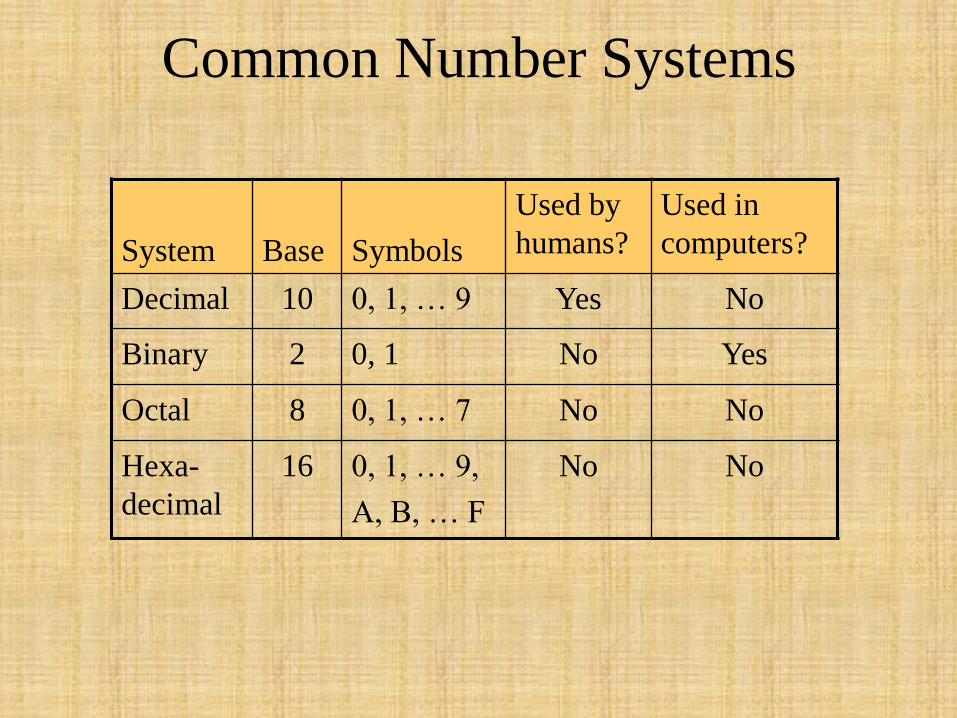
Common Number Systems
System
Base
Symbols
Used by
humans?
Used in
computers?
Decimal 10 0, 1, … 9 Yes No
Binary 2 0, 1 No Yes
Octal 8 0, 1, … 7 No No
Hexa-
decimal
16 0, 1, … 9,
A, B, … F
No No
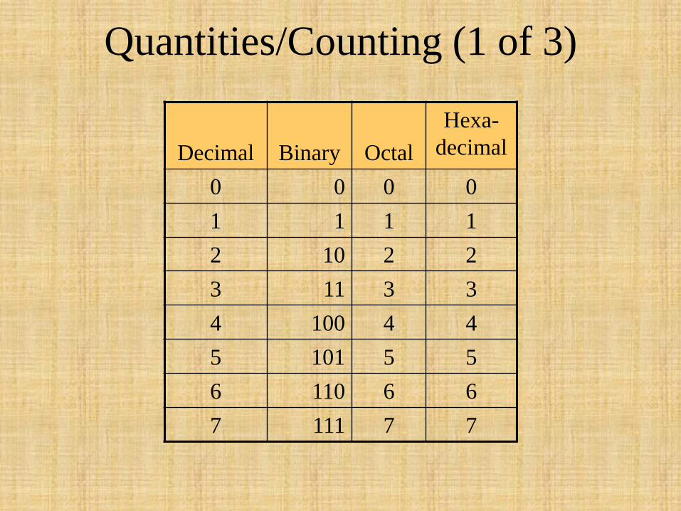
Quantities/Counting (1 of 3)
Decimal
Binary
Octal
Hexa-
decimal
0 0 0 0
1 1 1 1
2 10 2 2
3 11 3 3
4 100 4 4
5 101 5 5
6 110 6 6
7 111 7 7
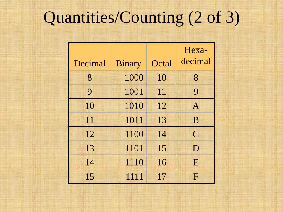
Quantities/Counting (2 of 3)
Decimal
Binary
Octal
Hexa-
decimal
8 1000 10 8
9 1001 11 9
10 1010 12 A
11 1011 13 B
12 1100 14 C
13 1101 15 D
14 1110 16 E
15 1111 17 F
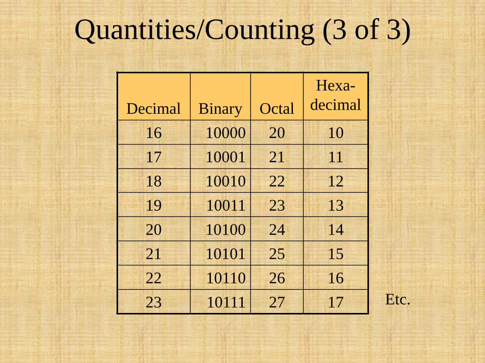
Quantities/Counting (3 of 3)
Decimal
Binary
Octal
Hexa-
decimal
16 10000 20 10
17 10001 21 11
18 10010 22 12
19 10011 23 13
20 10100 24 14
21 10101 25 15
22 10110 26 16
23 10111 27 17 Etc.
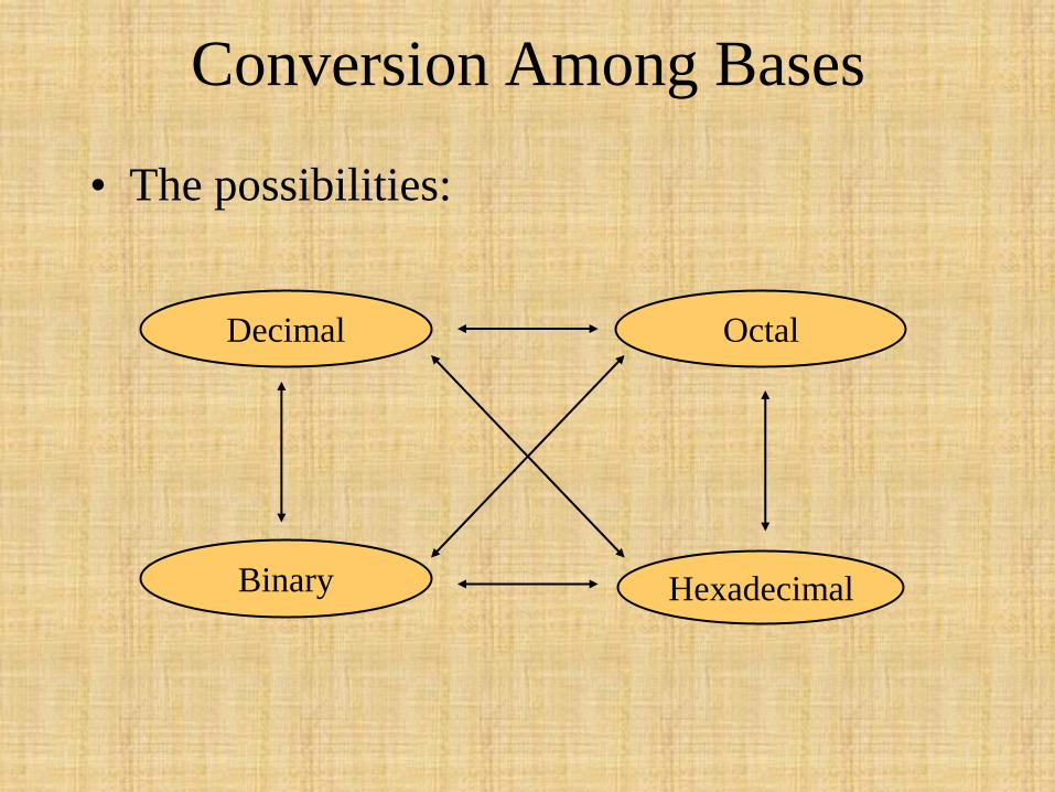
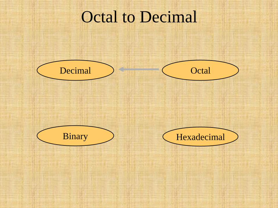
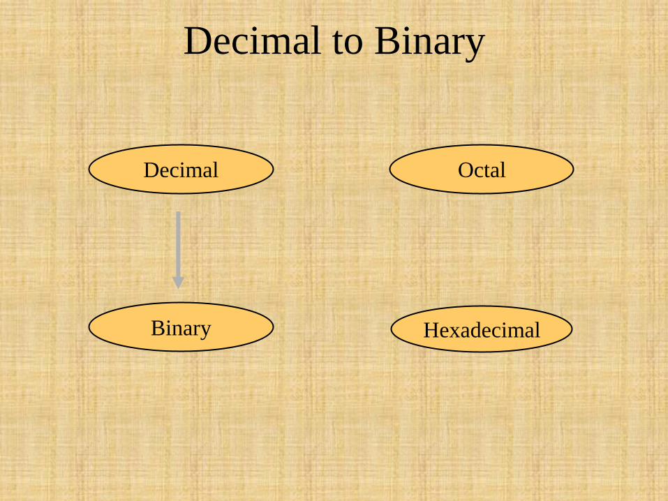
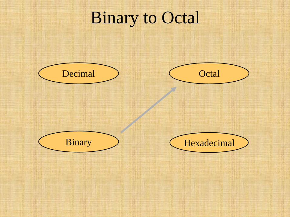
Conversion Among Bases
• The possibilities:
Hexadecimal
Decimal Octal
Binary
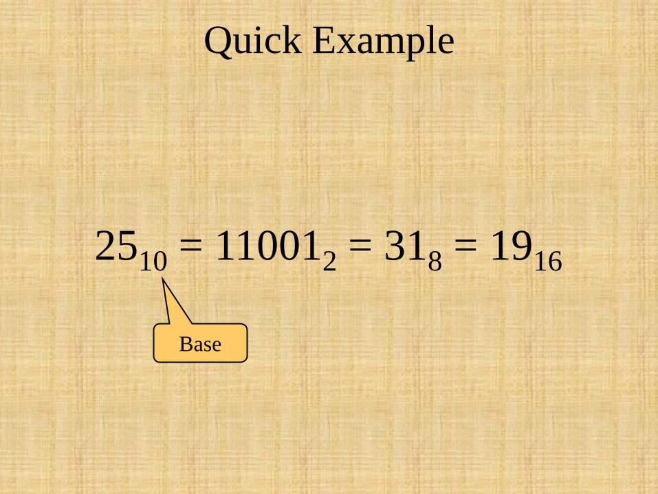
Quick Example
2510 = 110012 = 318 = 1916
Base

Decimal to Decimal (just for fun)
Hexadecimal
Decimal Octal
Binary

12510 => 5 x 100 = 5
2 x 101 = 20
1 x 102 = 100
125
Base
Weight
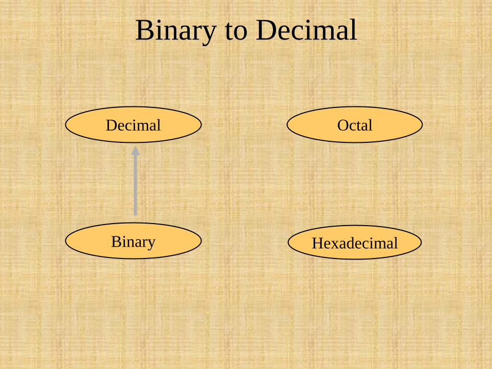
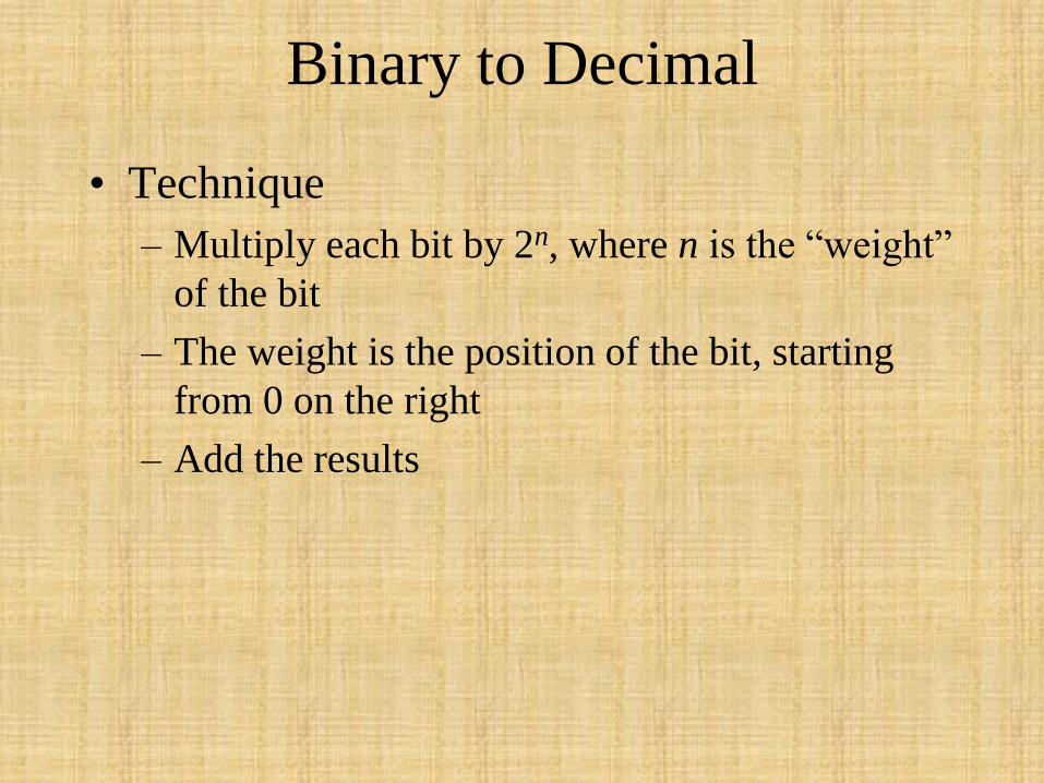
Binary to Decimal
Hexadecimal
Decimal Octal
Binary
Binary to Decimal
• Technique
– Multiply each bit by 2n, where n is the “weight”
of the bit
– The weight is the position of the bit, starting
from 0 on the right
– Add the results
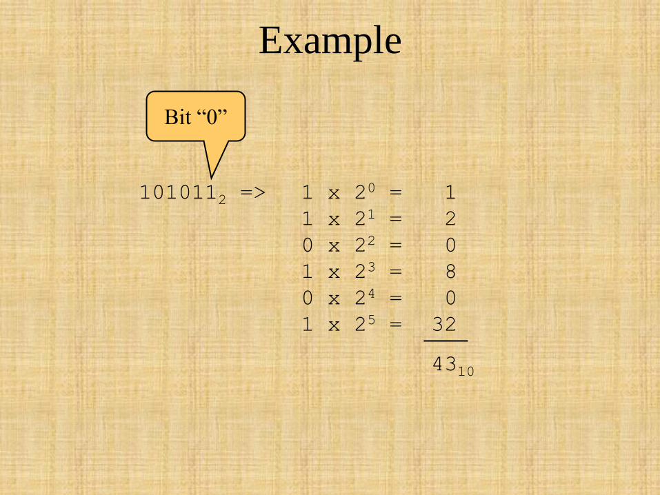
Example
1010112 => 1 x 20 = 1
1 x 21 = 2
0 x 22 = 0
1 x 23 = 8
0 x 24 = 0
1 x 25 = 32
4310
Bit “0”
Octal to Decimal
Hexadecimal
Decimal Octal
Binary
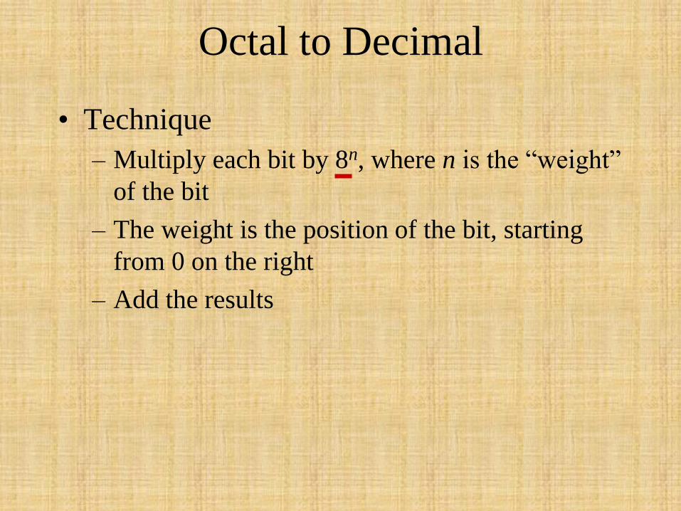
Octal to Decimal
• Technique
– Multiply each bit by 8n, where n is the “weight”
of the bit
– The weight is the position of the bit, starting
from 0 on the right
– Add the results
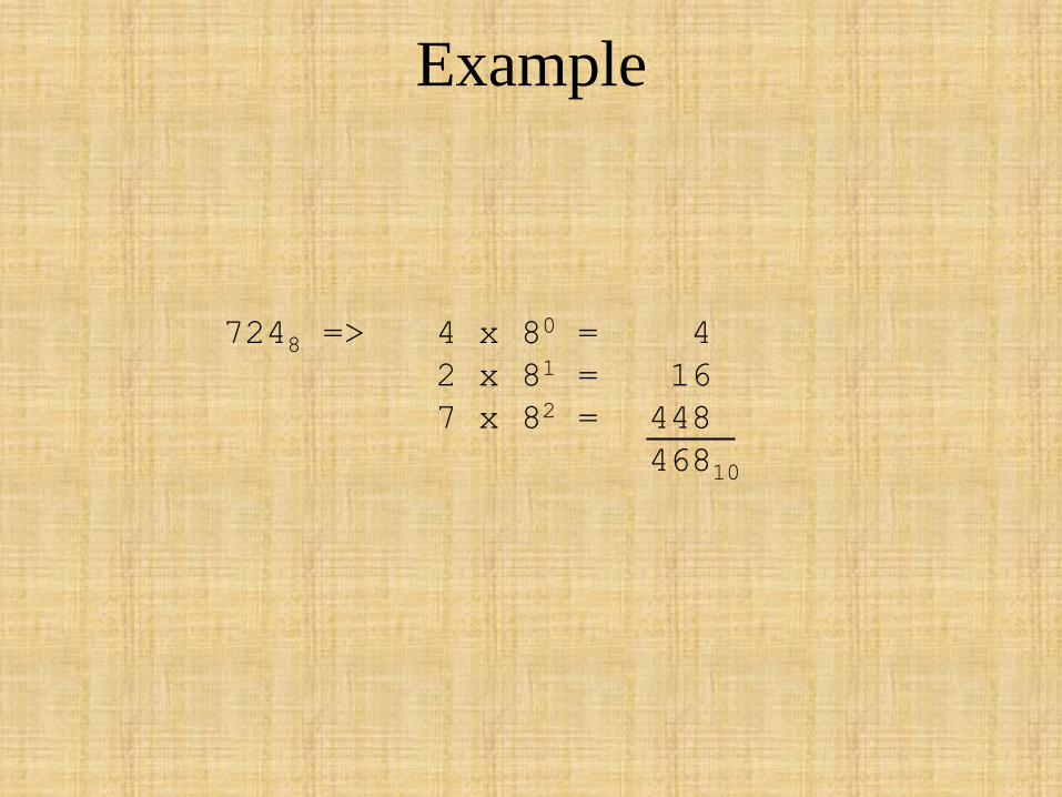
Example
7248 => 4 x 80 = 4
2 x 81 = 16
7 x 82 = 448
46810
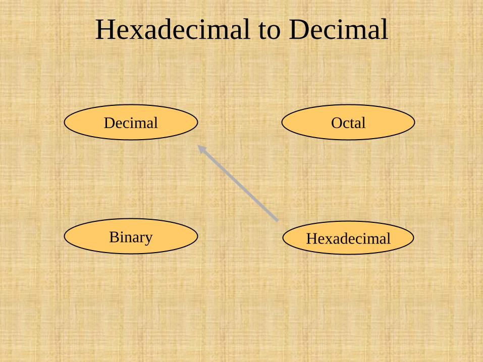
Hexadecimal to Decimal
Hexadecimal
Decimal Octal
Binary
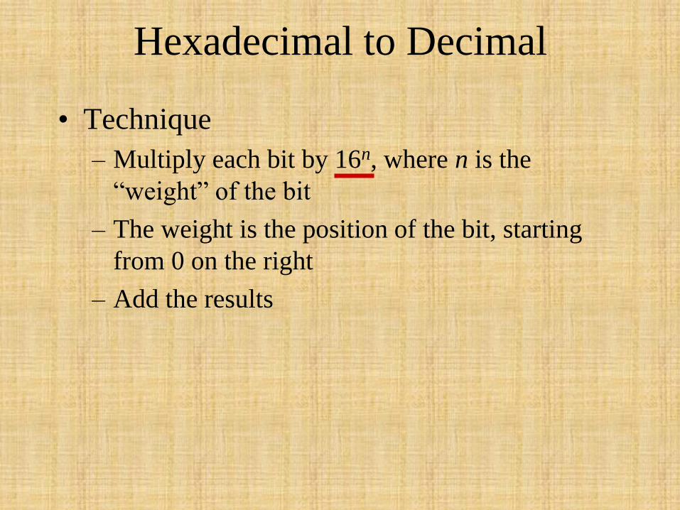
Hexadecimal to Decimal
• Technique
– Multiply each bit by 16n, where n is the
“weight” of the bit
– The weight is the position of the bit, starting
from 0 on the right
– Add the results
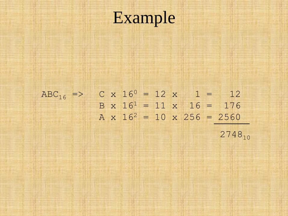
Example
ABC16 => C x 160 = 12 x 1 = 12
B x 161 = 11 x 16 = 176
A x 162 = 10 x 256 = 2560
274810
Decimal to Binary
Hexadecimal
Decimal Octal
Binary
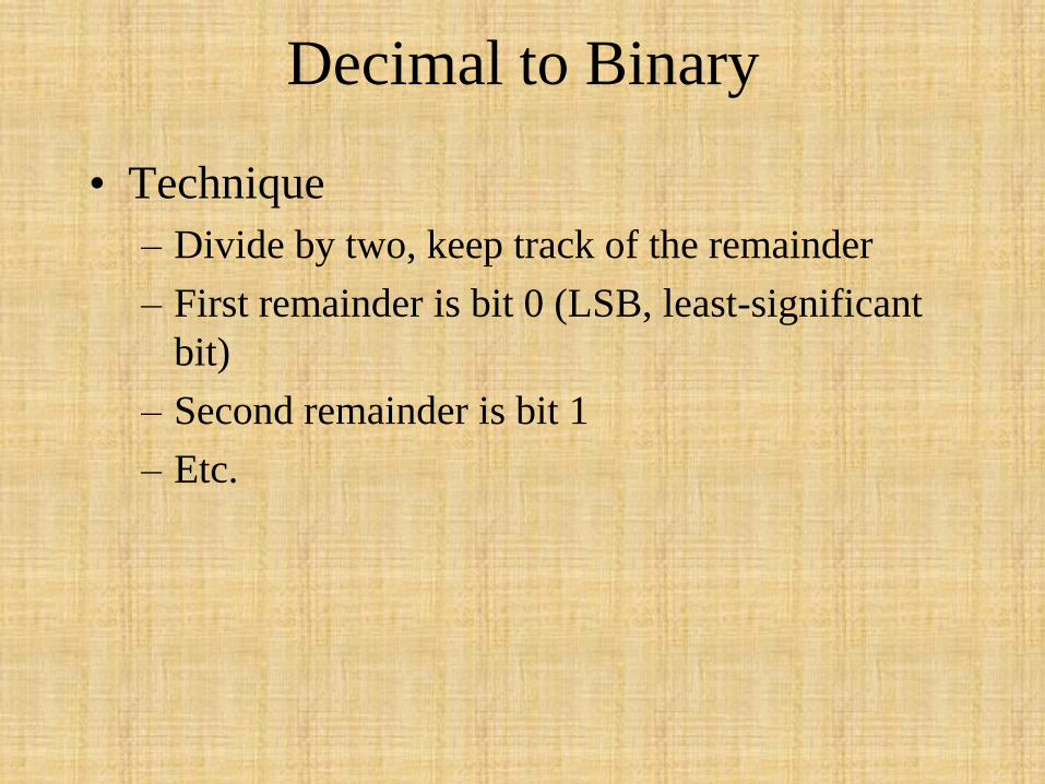
Decimal to Binary
• Technique
– Divide by two, keep track of the remainder
– First remainder is bit 0 (LSB, least-significant
bit)
– Second remainder is bit 1
– Etc.
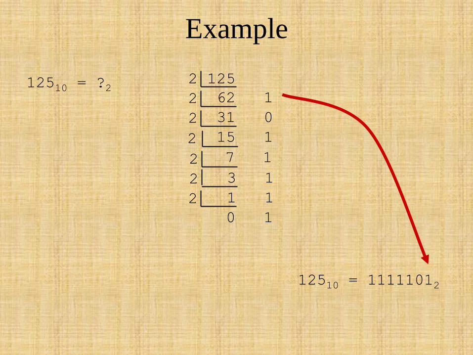
Example
12510 = ?2 2 125
62 1 2
31 0 2
15 1 2
7 1 2
3 1 2
1 1 2
0 1
12510 = 11111012
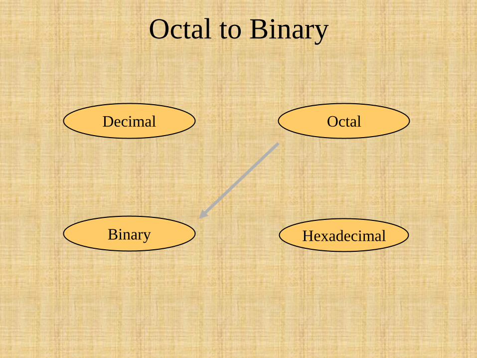
Octal to Binary
Hexadecimal
Decimal Octal
Binary

Octal to Binary
• Technique
– Convert each octal digit to a 3-bit equivalent
binary representation
Example
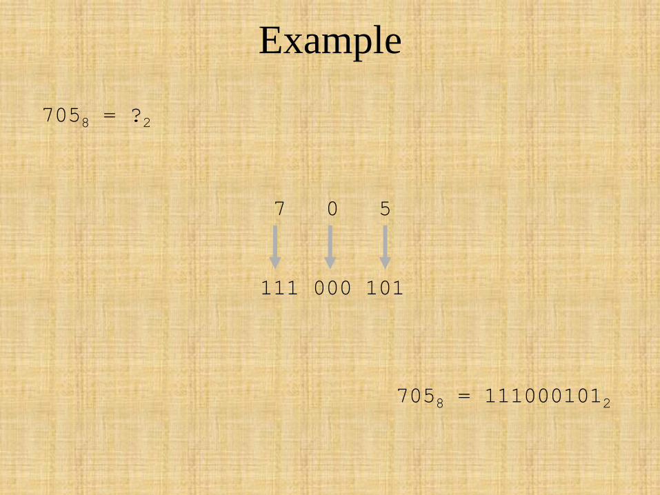
7058 = ?2
7 0 5
111 000 101
7058 = 1110001012

Hexadecimal to Binary
Hexadecimal
Decimal Octal
Binary
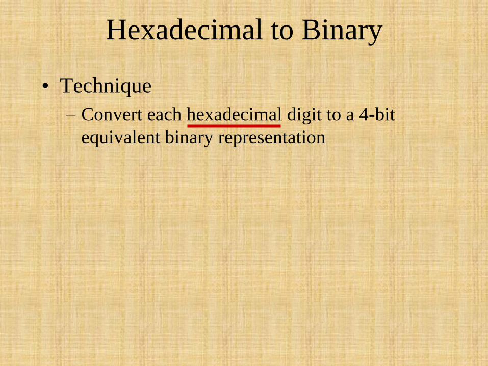
Hexadecimal to Binary
• Technique
– Convert each hexadecimal digit to a 4-bit
equivalent binary representation
Example
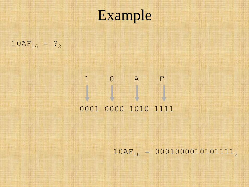
10AF16 = ?2
1 0 A F
0001 0000 1010 1111
10AF16 = 00010000101011112
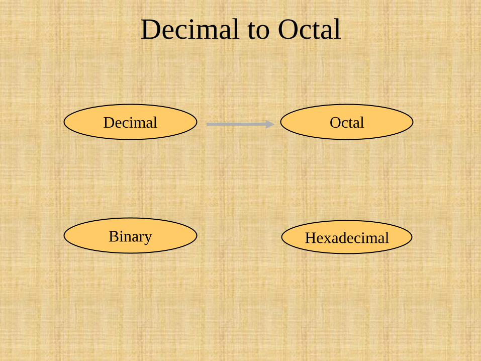
Decimal to Octal
Hexadecimal
Decimal Octal
Binary
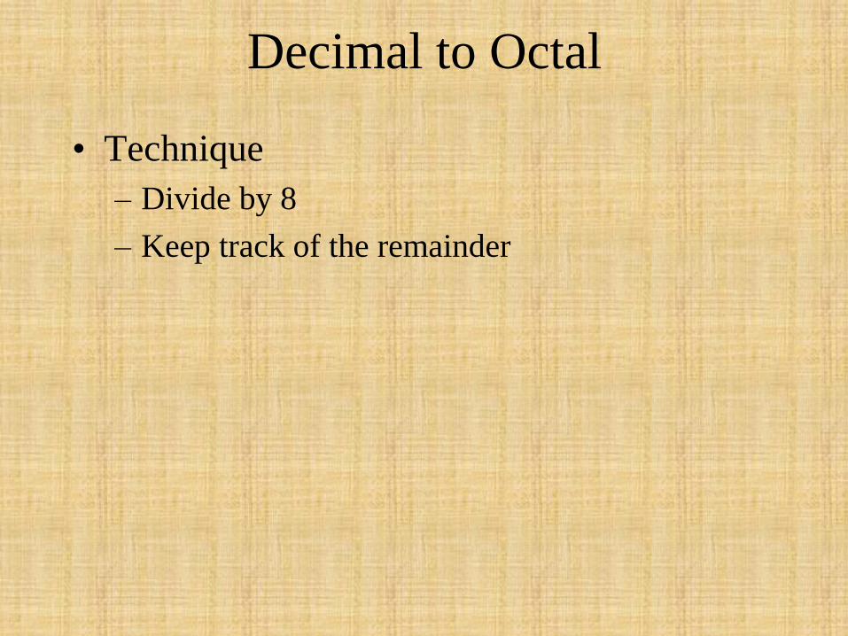
Decimal to Octal
• Technique
– Divide by 8
– Keep track of the remainder
Example
123410 = ?8
8 1234
154 2 8
19 2 8
2 3 8
0 2
123410 = 23228

Decimal to Hexadecimal
Hexadecimal
Decimal Octal
Binary
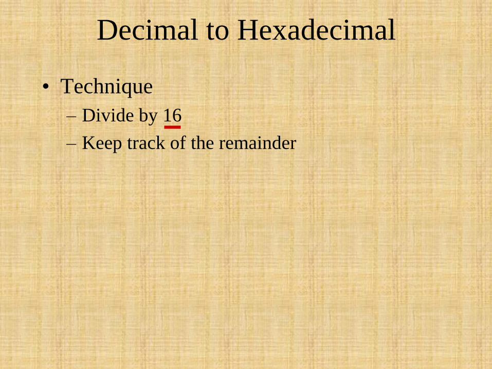
Decimal to Hexadecimal
• Technique
– Divide by 16
– Keep track of the remainder
Example
123410 = ?16
123410 = 4D216
16 1234
77 2 16
4 13 = D 16
0 4
Binary to Octal
Hexadecimal
Decimal Octal
Binary
Binary to Octal
• Technique
– Group bits in threes, starting on right
– Convert to octal digits

Example
10110101112 = ?8
1 011 010 111
1 3 2 7
10110101112 = 13278
Binary to Hexadecimal
Hexadecimal
Decimal Octal
Binary
Binary to Hexadecimal
• Technique
– Group bits in fours, starting on right
– Convert to hexadecimal digits
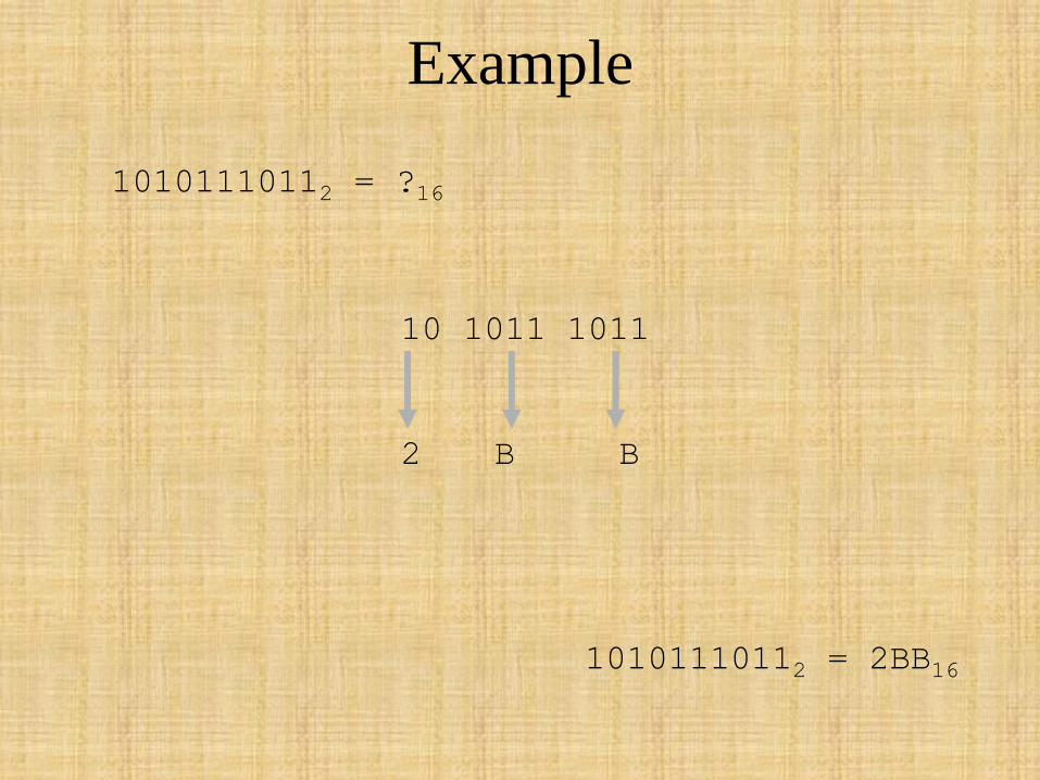
Example
10101110112 = ?16
10 1011 1011
2 B B
10101110112 = 2BB16
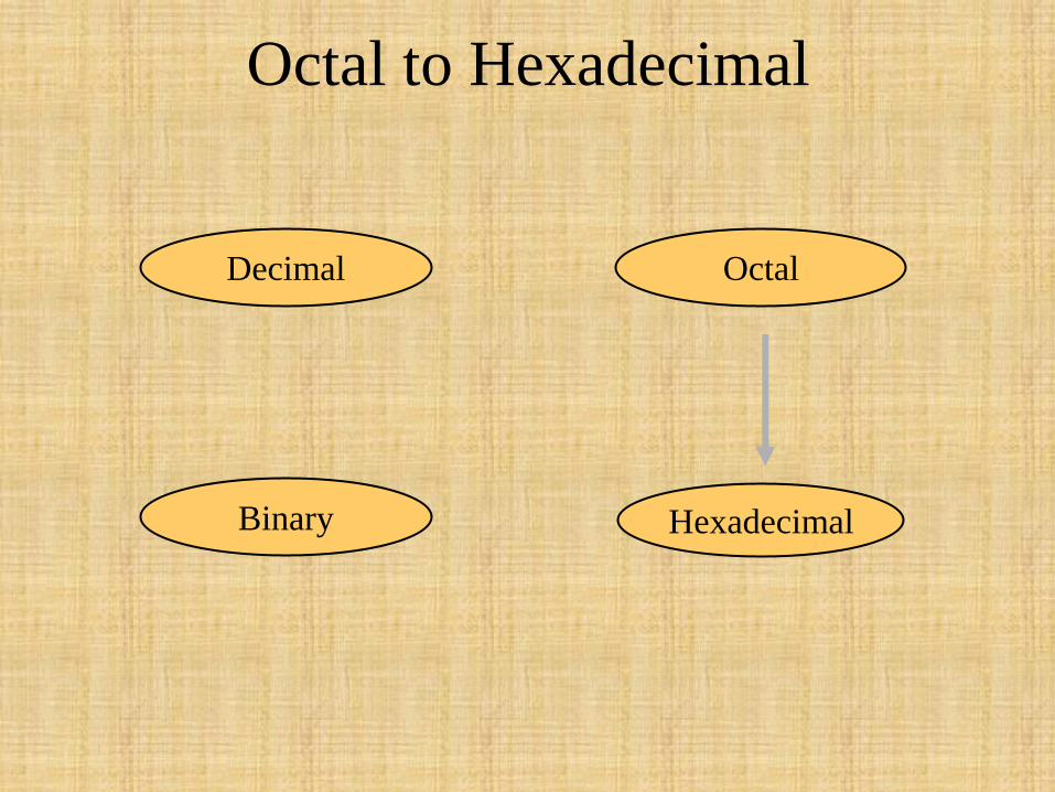
Octal to Hexadecimal
Hexadecimal
Decimal Octal
Binary

Octal to Hexadecimal
• Technique
– Use binary as an intermediary
Example
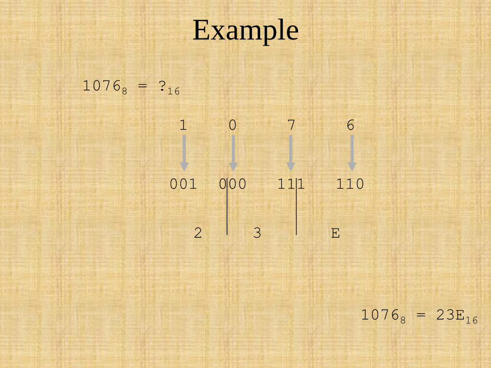
10768 = ?16
1 0 7 6
001 000 111 110
2 3 E
10768 = 23E16
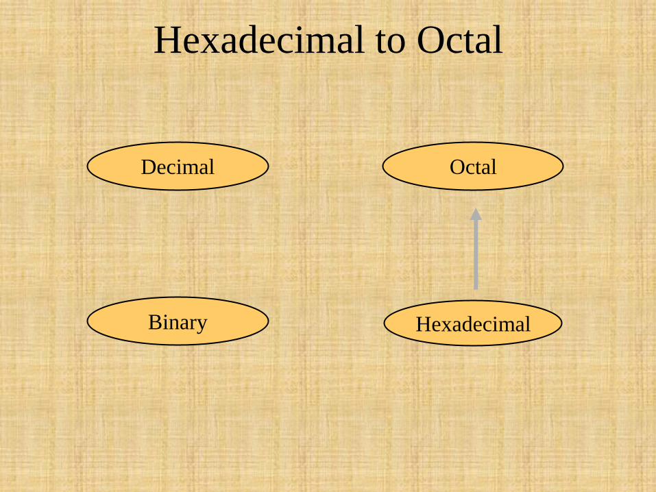
Hexadecimal to Octal
Hexadecimal
Decimal Octal
Binary
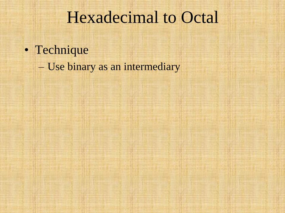
Hexadecimal to Octal
• Technique
– Use binary as an intermediary
Example
1F0C16 = ?8
1 F 0 C
0001 1111 0000 1100
1 7 4 1 4
1F0C16 = 174148
Exercise – Convert ...
Decimal
Binary
Octal
Hexa-
decimal
33
1110101
703
1AF
Exercise – Convert …
Decimal
Binary
Octal
Hexa-
decimal
33 100001 41 21
117 1110101 165 75
451 111000011 703 1C3
431 110101111 657 1AF
Answer
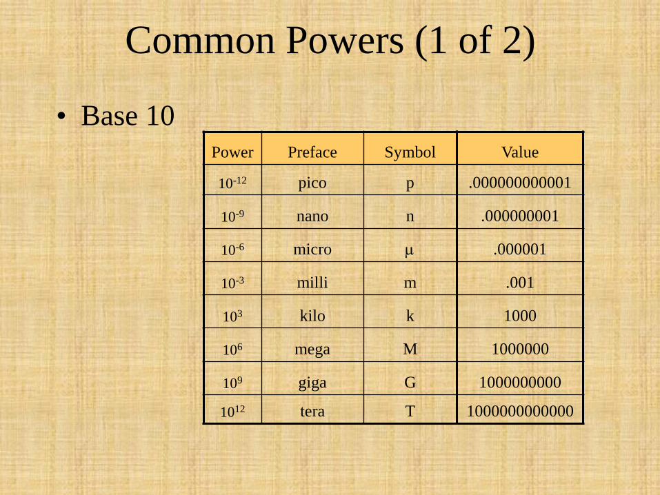
Common Powers (1 of 2)
• Base 10 Power Preface Symbol
10-12 pico p
10-9 nano n
10-6 micro
10-3 milli m
103 kilo k
106 mega M
109 giga G
1012 tera T
Value
.000000000001
.000000001
.000001
.001
1000
1000000
1000000000
1000000000000
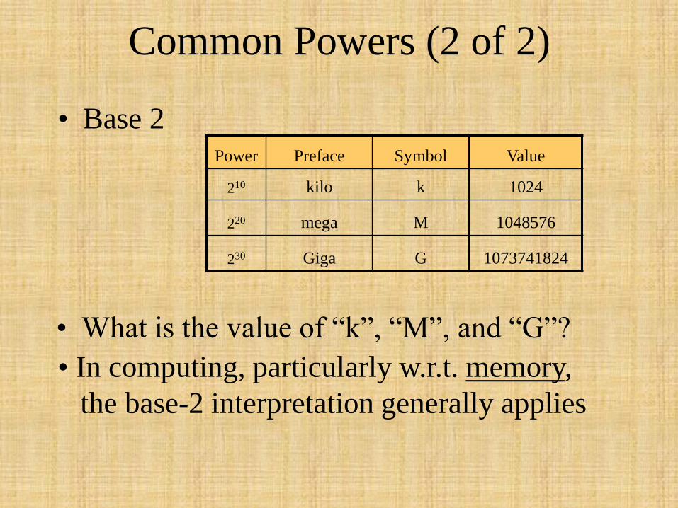
Common Powers (2 of 2)
• Base 2 Power Preface Symbol
210 kilo k
220 mega M
230 Giga G
Value
1024
1048576
1073741824
• What is the value of “k”, “M”, and “G”?
• In computing, particularly w.r.t. memory,
the base-2 interpretation generally applies
Example
/ 230 =
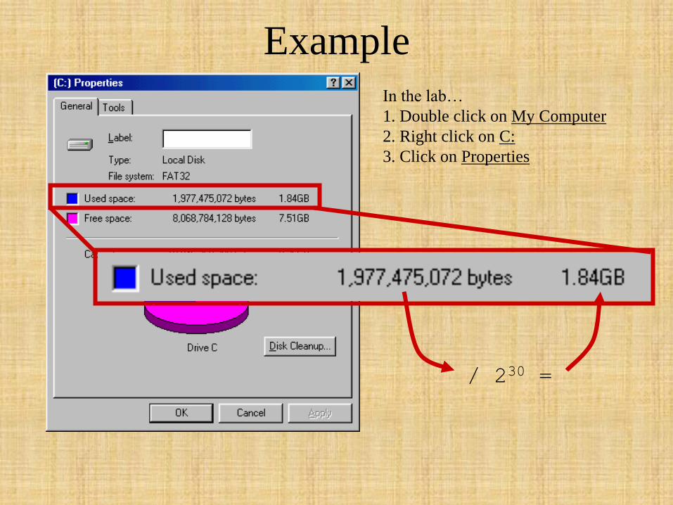
In the lab…
1. Double click on My Computer
2. Right click on C:
3. Click on Properties
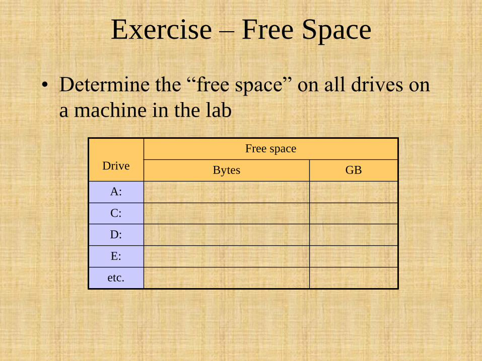
Exercise – Free Space
• Determine the “free space” on all drives on
a machine in the lab
Drive
Free space
Bytes GB
A:
C:
D:
E:
etc.
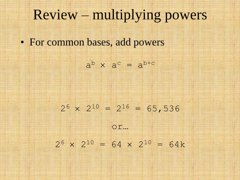
Review – multiplying powers
• For common bases, add powers
26 210 = 216 = 65,536
or…
26 210 = 64 210 = 64k
ab ac = ab+c
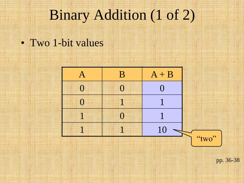
Binary Addition (1 of 2)
• Two 1-bit values
pp. 36-38
A B A + B
0 0 0
0 1 1
1 0 1
1 1 10 “two”
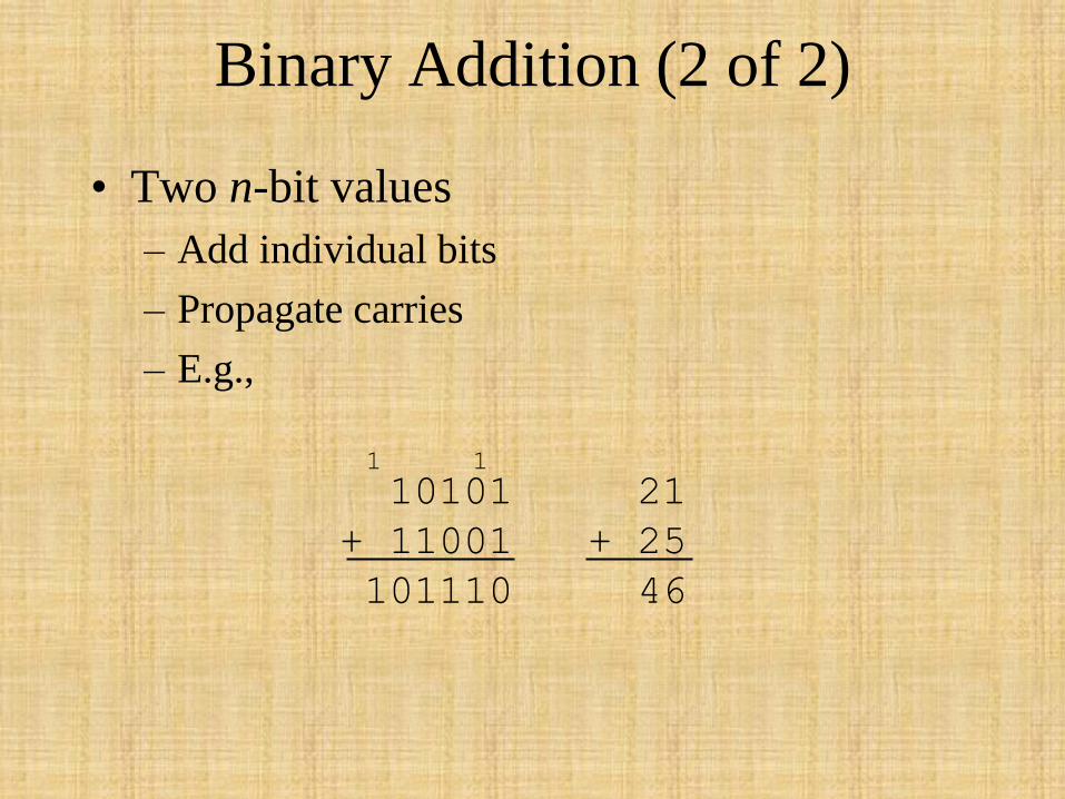
Binary Addition (2 of 2)
• Two n-bit values
– Add individual bits
– Propagate carries
– E.g.,
10101 21
+ 11001 + 25
101110 46
1 1
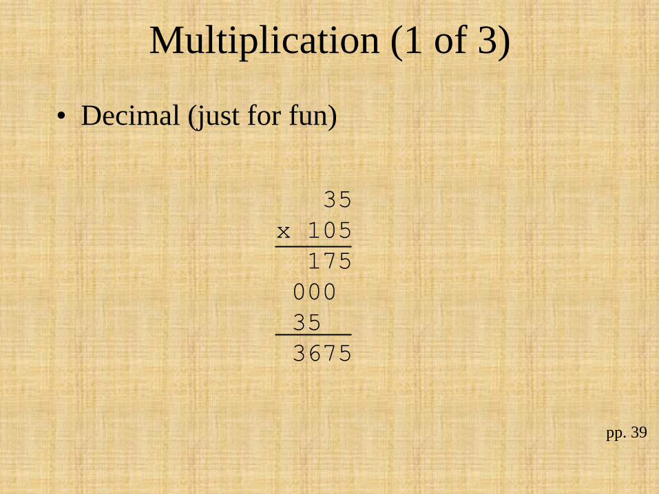
Multiplication (1 of 3)
• Decimal (just for fun)
pp. 39
35
x 105
175
000
35
3675
Multiplication (2 of 3)
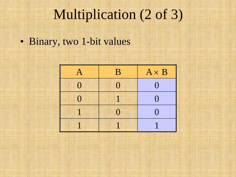
• Binary, two 1-bit values
A B A B
0 0 0
0 1 0
1 0 0
1 1 1
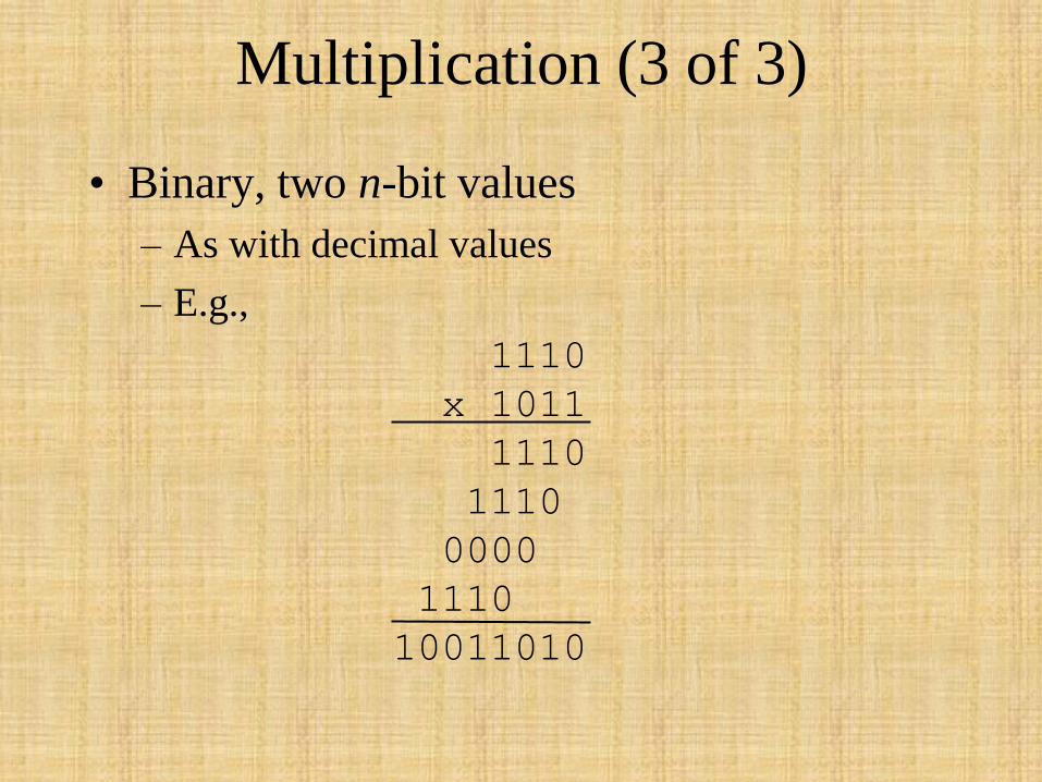
Multiplication (3 of 3)
• Binary, two n-bit values
– As with decimal values
– E.g.,
1110
x 1011
1110
1110
0000
1110
10011010
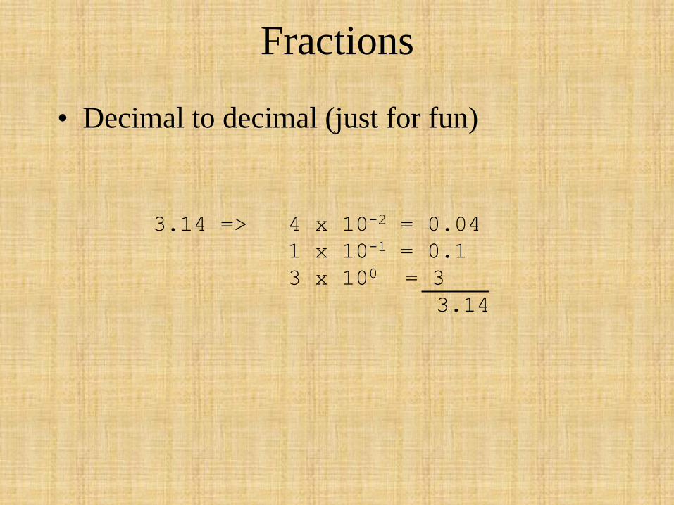
Fractions
• Decimal to decimal (just for fun)
3.14 => 4 x 10-2 = 0.04
1 x 10-1 = 0.1
3 x 100 = 3
3.14
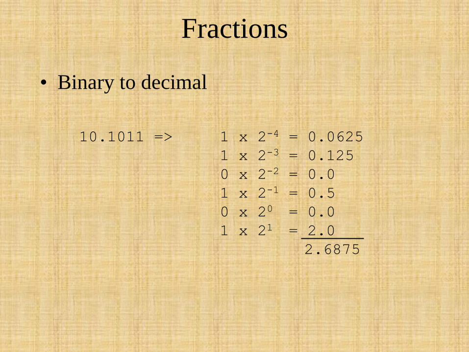
Fractions
• Binary to decimal
10.1011 => 1 x 2-4 = 0.0625
1 x 2-3 = 0.125
0 x 2-2 = 0.0
1 x 2-1 = 0.5
0 x 20 = 0.0
1 x 21 = 2.0
2.6875
Fractions
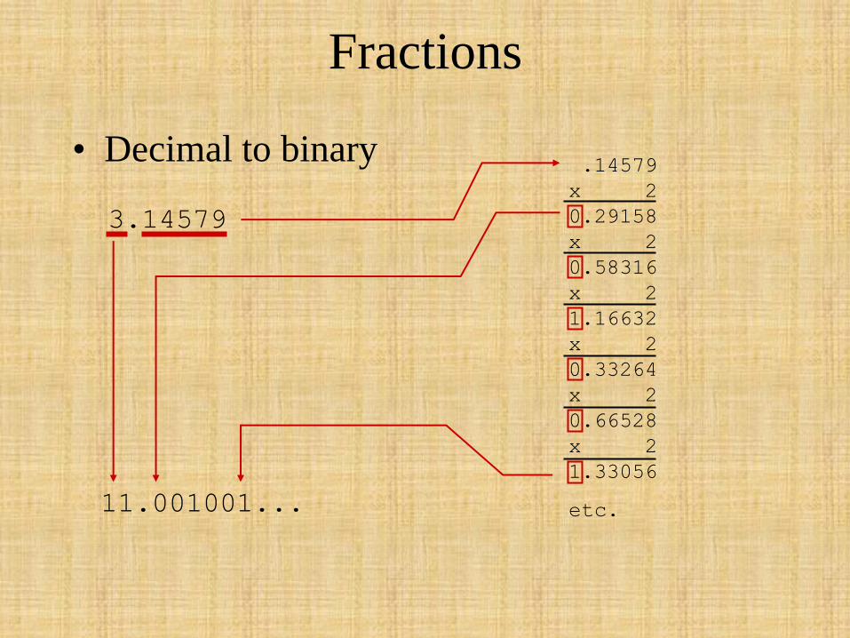
• Decimal to binary
3.14579
.14579
x 2
0.29158
x 2
0.58316
x 2
1.16632
x 2
0.33264
x 2
0.66528
x 2
1.33056
etc. 11.001001...
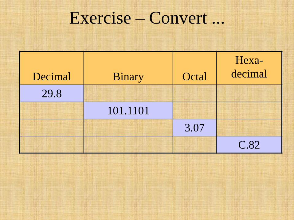
Exercise – Convert ...
Decimal
Binary
Octal
Hexa-
decimal
29.8
101.1101
3.07
C.82
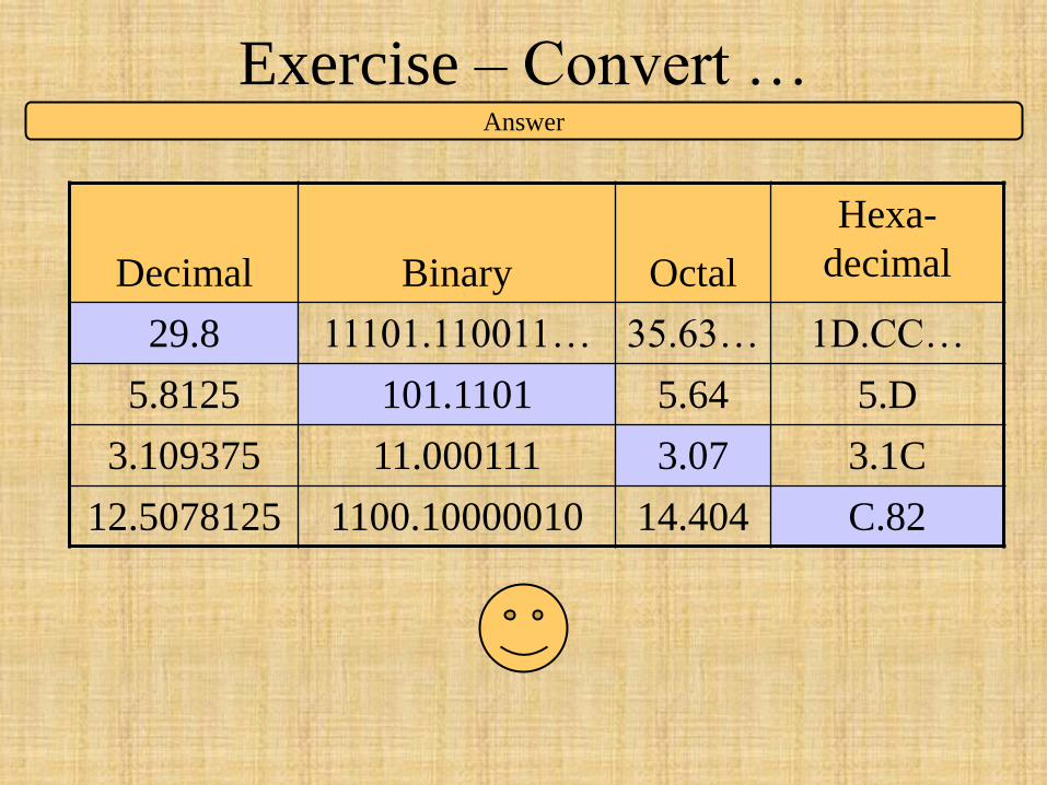
Exercise – Convert …
Decimal
Binary
Octal
Hexa-
decimal
29.8 11101.110011… 35.63… 1D.CC…
5.8125 101.1101 5.64 5.D
3.109375 11.000111 3.07 3.1C
12.5078125 1100.10000010 14.404 C.82
Answer

Thank you
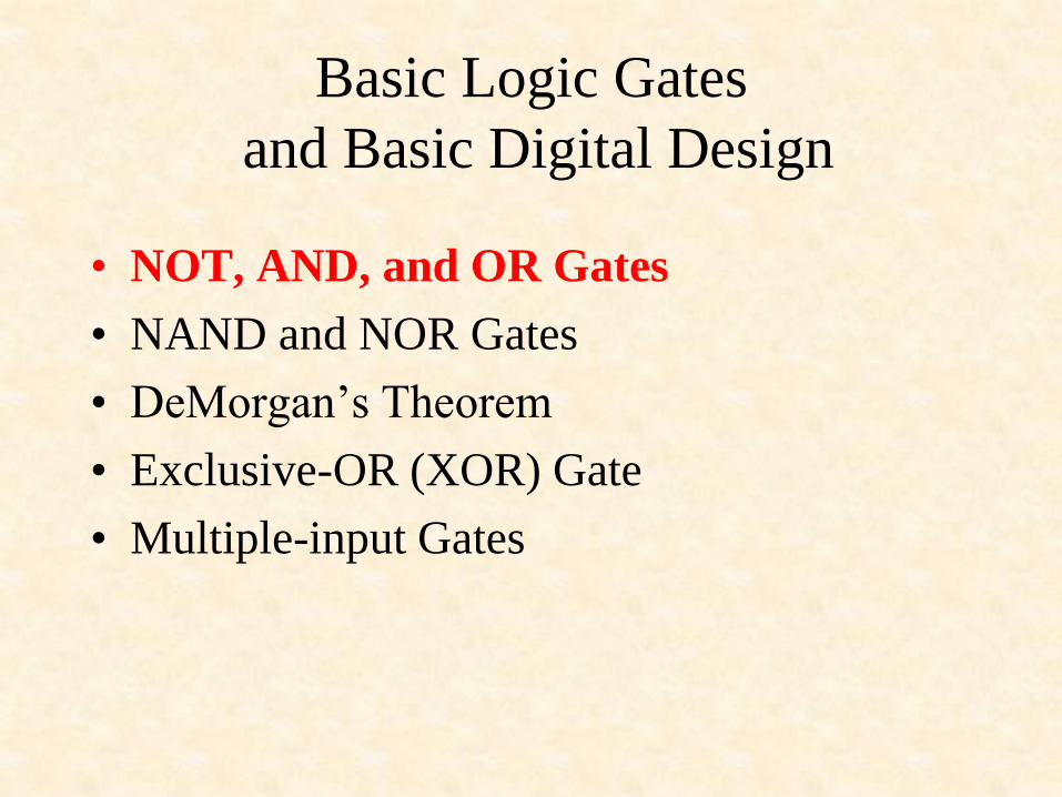
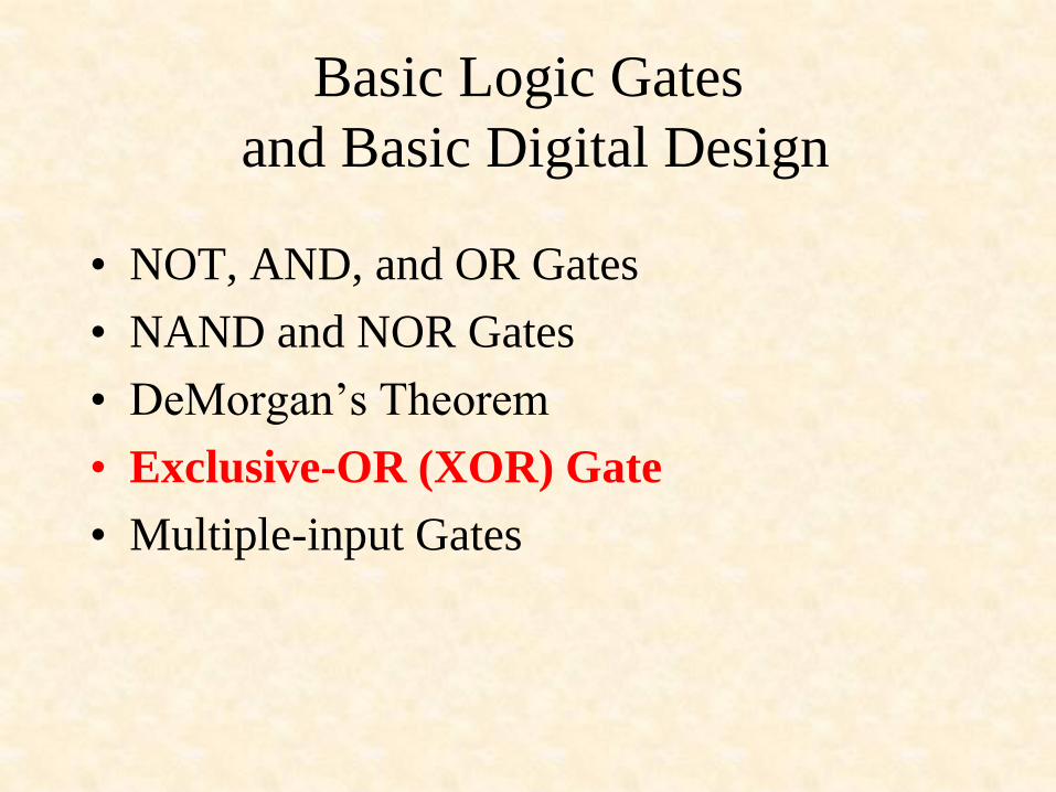
Basic Logic Gates
and Basic Digital Design
• NOT, AND, and OR Gates
• NAND and NOR Gates
• DeMorgan’s Theorem
• Exclusive-OR (XOR) Gate
• Multiple-input Gates
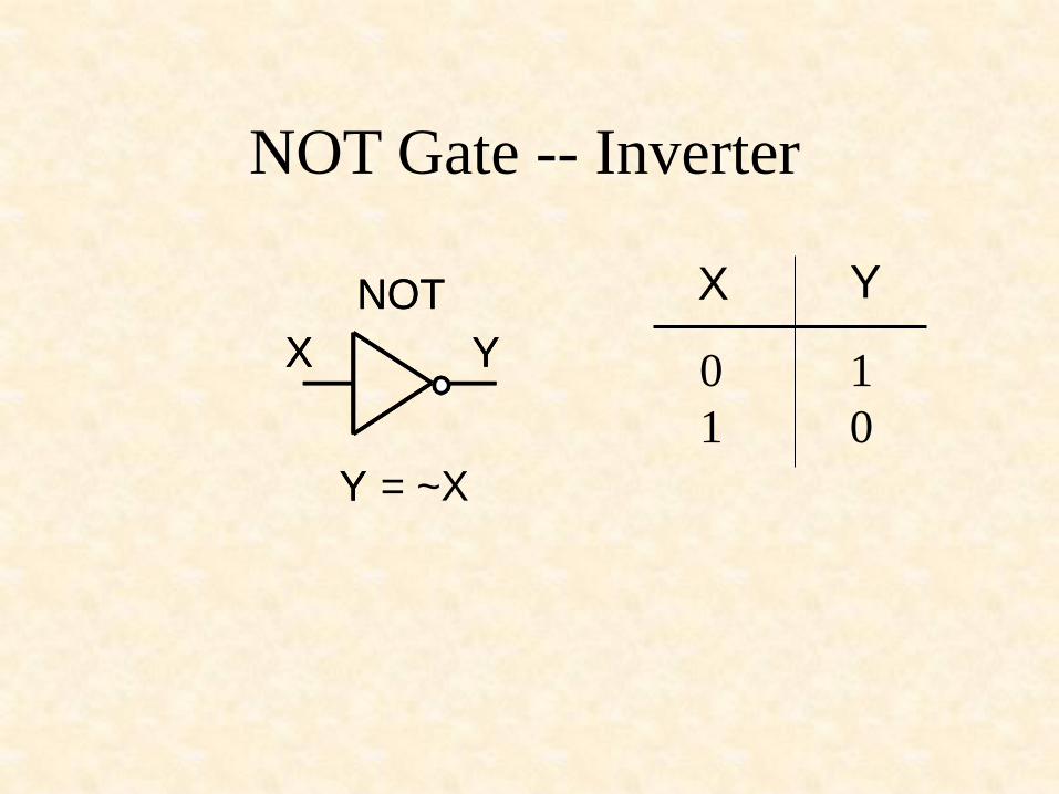
NOT Gate -- Inverter
X Y
0
1
1
0
X Y
Y
NOT
X Y
Y = ~X
NOT
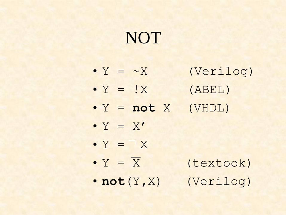
• Y = ~X (Verilog)
• Y = !X (ABEL)
• Y = not X (VHDL)
• Y = X’
• Y = X
• Y = X (textook)
• not(Y,X) (Verilog)
NOT
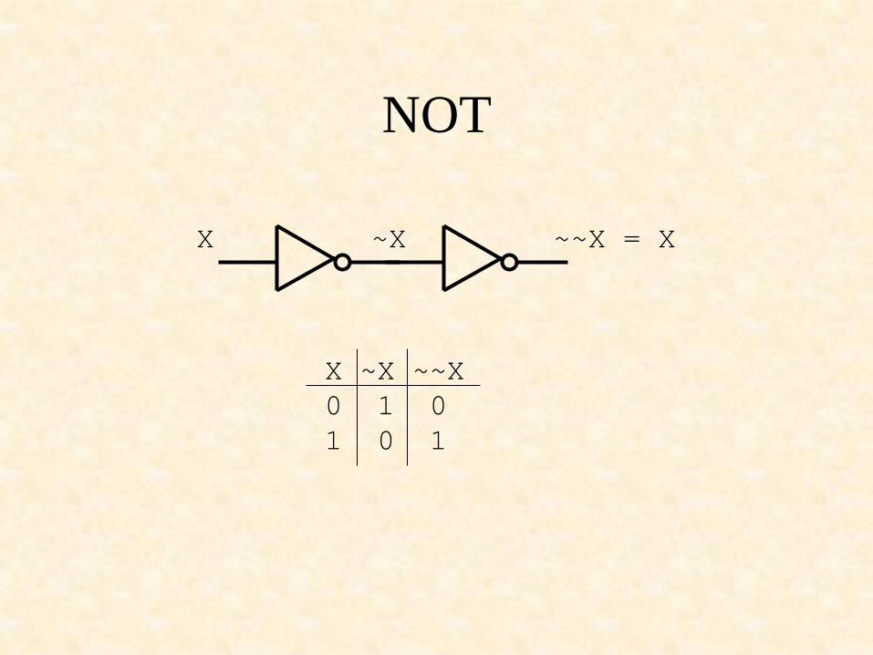
NOT
X ~X ~~X = X
X ~X ~~X
0 1 0
1 0 1
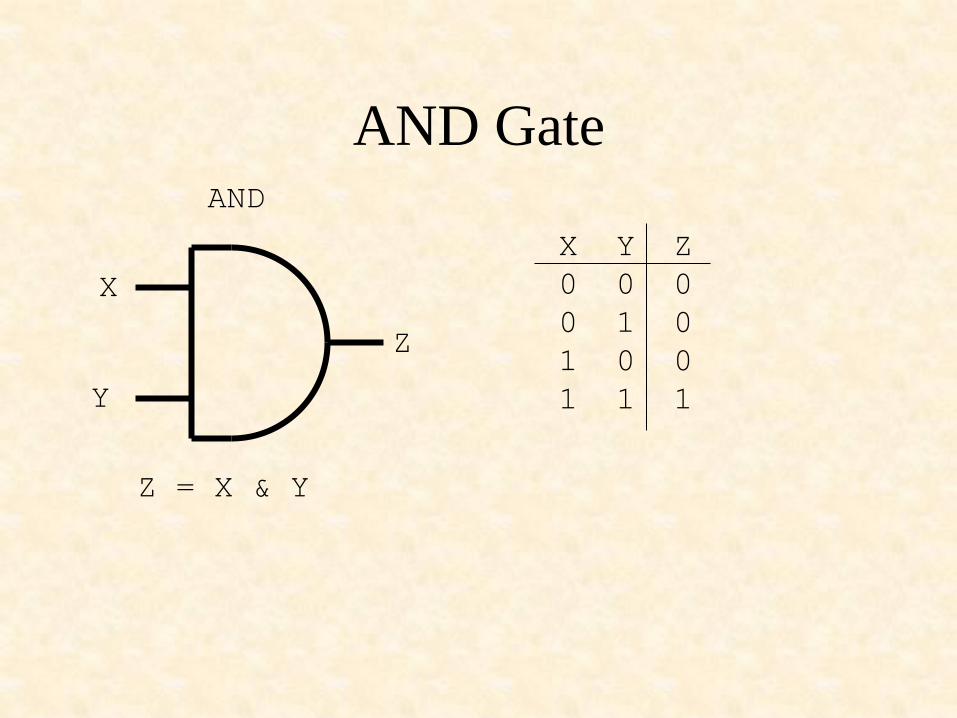
AND Gate AND
X
Y
Z
Z = X & Y
X Y Z
0 0 0
0 1 0
1 0 0
1 1 1
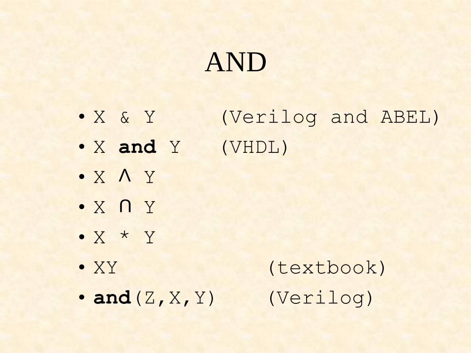
• X & Y (Verilog and ABEL)
• X and Y (VHDL)
• X Y
• X Y
• X * Y
• XY (textbook)
• and(Z,X,Y) (Verilog)
AND
U
V
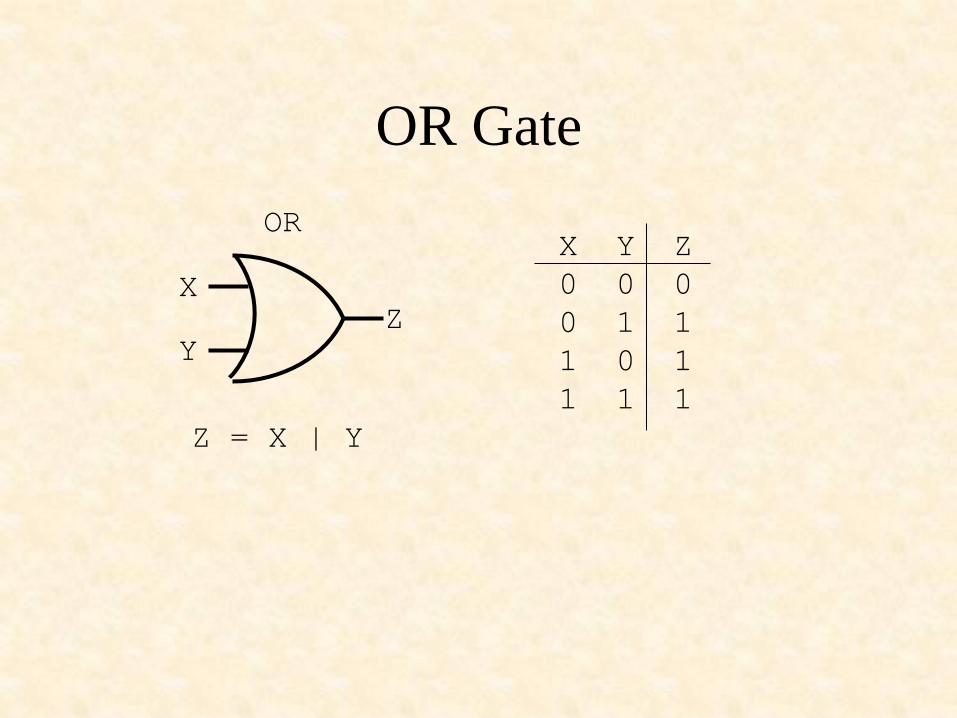
OR Gate
OR
X
Y Z
Z = X | Y
X Y Z
0 0 0
0 1 1
1 0 1
1 1 1
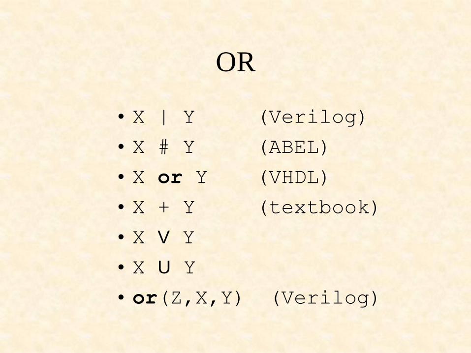
OR
• X | Y (Verilog)
• X # Y (ABEL)
• X or Y (VHDL)
• X + Y (textbook)
• X V Y
• X U Y
• or(Z,X,Y) (Verilog)
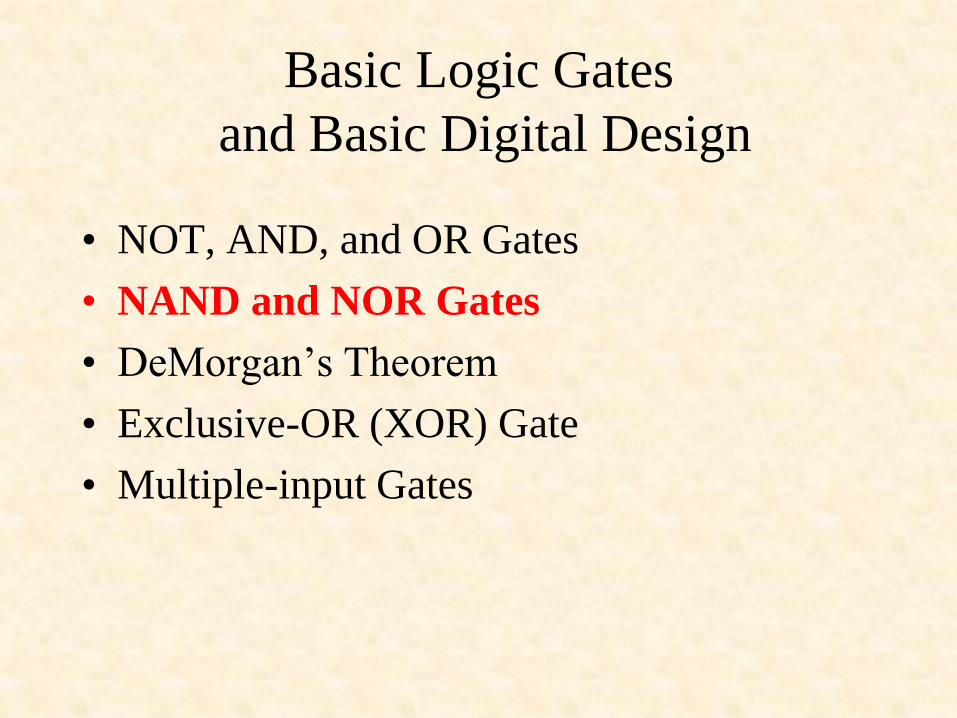
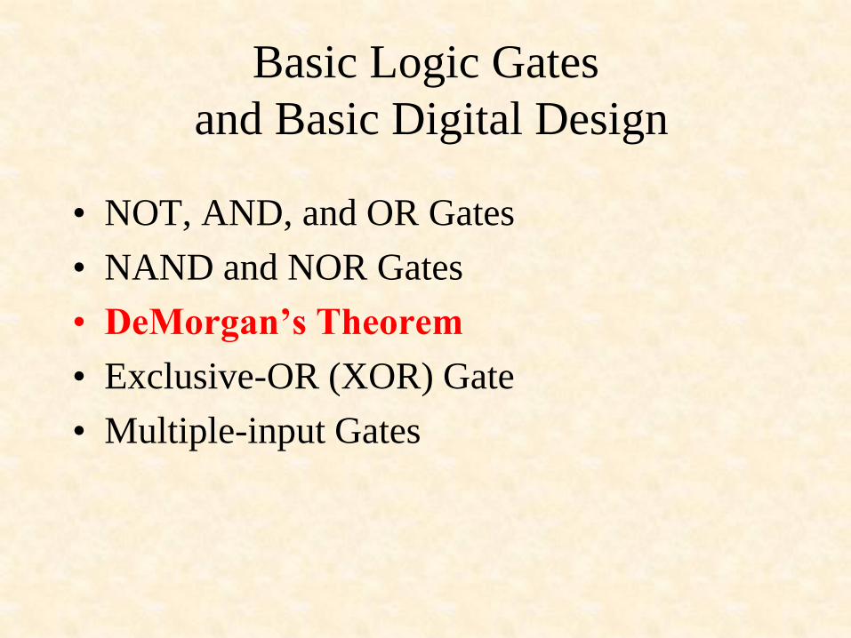
Basic Logic Gates
and Basic Digital Design
• NOT, AND, and OR Gates
• NAND and NOR Gates
• DeMorgan’s Theorem
• Exclusive-OR (XOR) Gate
• Multiple-input Gates

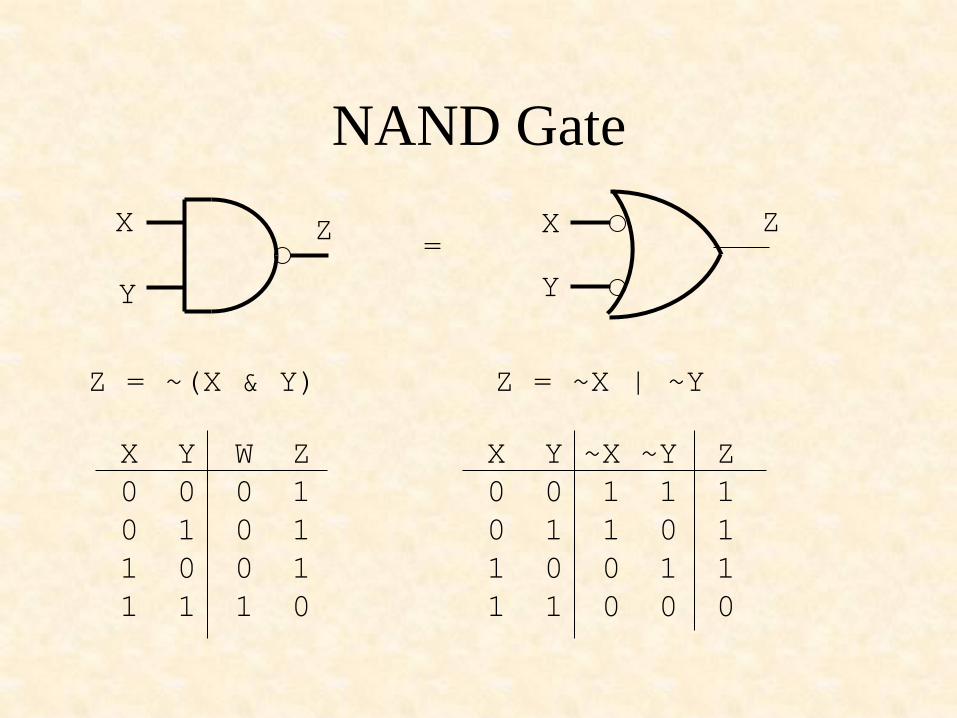
NAND Gate NAND
X
Y
Z
X Y Z
0 0 1
0 1 1
1 0 1
1 1 0
Z = ~(X & Y)
nand(Z,X,Y)
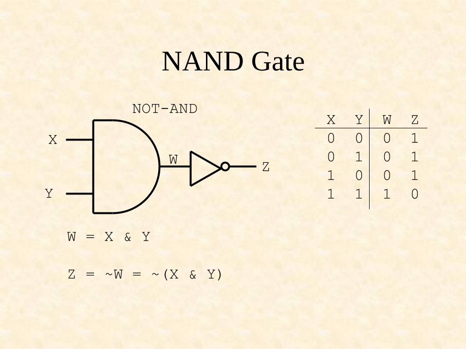
NAND Gate
NOT-AND
X
Y
Z
W = X & Y
Z = ~W = ~(X & Y)
X Y W Z
0 0 0 1
0 1 0 1
1 0 0 1
1 1 1 0
W
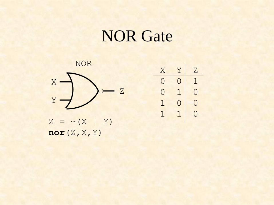
NOR Gate
NOR
X
Y Z
X Y Z
0 0 1
0 1 0
1 0 0
1 1 0 Z = ~(X | Y)
nor(Z,X,Y)
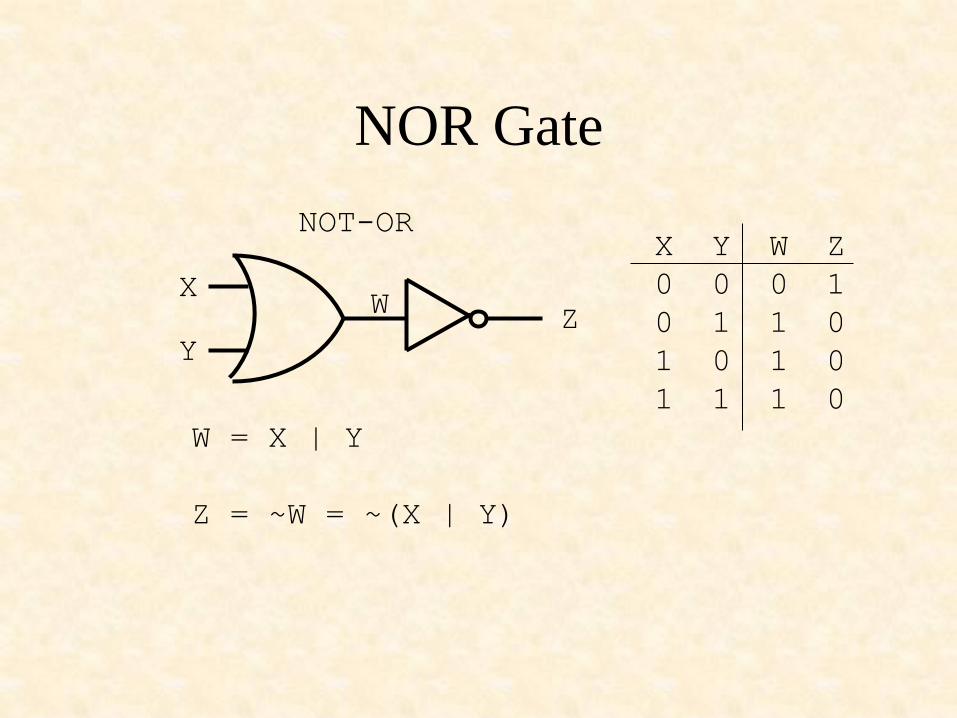
NOR Gate
NOT-OR
X
Y
W = X | Y
Z = ~W = ~(X | Y)
X Y W Z
0 0 0 1
0 1 1 0
1 0 1 0
1 1 1 0
Z W
Basic Logic Gates
and Basic Digital Design
• NOT, AND, and OR Gates
• NAND and NOR Gates
• DeMorgan’s Theorem
• Exclusive-OR (XOR) Gate
• Multiple-input Gates
NAND Gate
X
Y
X
Y
Z Z
Z = ~(X & Y) Z = ~X | ~Y
=
X Y W Z
0 0 0 1
0 1 0 1
1 0 0 1
1 1 1 0
X Y ~X ~Y Z
0 0 1 1 1
0 1 1 0 1
1 0 0 1 1
1 1 0 0 0
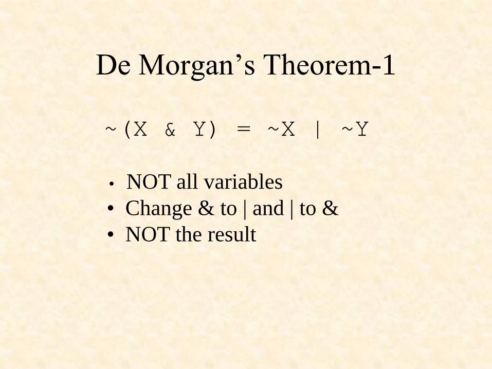
De Morgan’s Theorem-1
~(X & Y) = ~X | ~Y
• NOT all variables
• Change & to | and | to &
• NOT the result
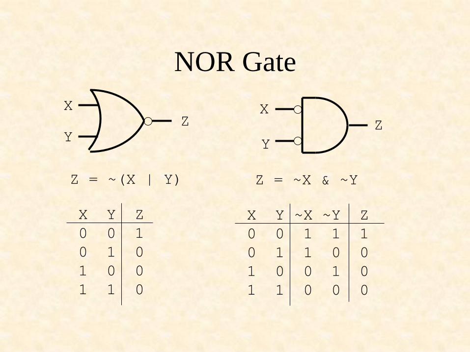
NOR Gate
X
Y Z
Z = ~(X | Y)
X Y Z
0 0 1
0 1 0
1 0 0
1 1 0
X
Y
Z
Z = ~X & ~Y
X Y ~X ~Y Z
0 0 1 1 1
0 1 1 0 0
1 0 0 1 0
1 1 0 0 0

De Morgan’s Theorem-2
~(X | Y) = ~X & ~Y
• NOT all variables
• Change & to | and | to &
• NOT the result
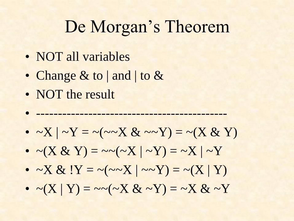
De Morgan’s Theorem
• NOT all variables
• Change & to | and | to &
• NOT the result
• --------------------------------------------
• ~X | ~Y = ~(~~X & ~~Y) = ~(X & Y)
• ~(X & Y) = ~~(~X | ~Y) = ~X | ~Y
• ~X & !Y = ~(~~X | ~~Y) = ~(X | Y)
• ~(X | Y) = ~~(~X & ~Y) = ~X & ~Y
Basic Logic Gates
and Basic Digital Design
• NOT, AND, and OR Gates
• NAND and NOR Gates
• DeMorgan’s Theorem
• Exclusive-OR (XOR) Gate
• Multiple-input Gates
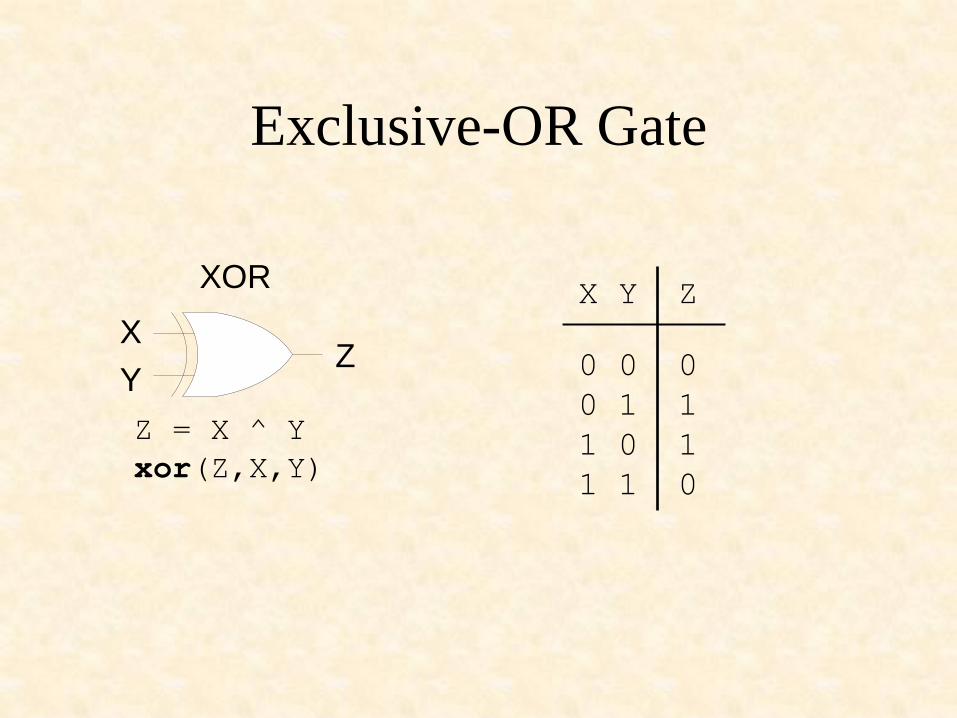
Exclusive-OR Gate
X Y Z XOR
X
Y Z 0 0 0
0 1 1
1 0 1
1 1 0
Z = X ^ Y
xor(Z,X,Y)
XOR
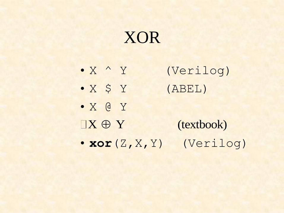
• X ^ Y (Verilog)
• X $ Y (ABEL)
• X @ Y
• xor(Z,X,Y) (Verilog)
X Y (textbook)
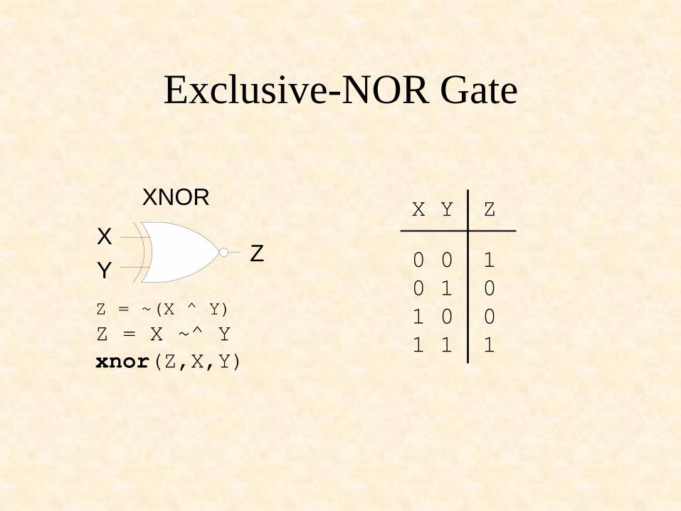
Exclusive-NOR Gate
X Y Z XNOR
X
Y Z 0 0 1
0 1 0
1 0 0
1 1 1
Z = ~(X ^ Y)
Z = X ~^ Y
xnor(Z,X,Y)
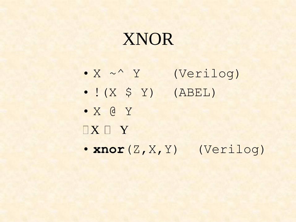
XNOR
• X ~^ Y (Verilog)
• !(X $ Y) (ABEL)
• X @ Y
• xnor(Z,X,Y) (Verilog)
X Y
Basic Logic Gates
and Basic Digital Design
• NOT, AND, and OR Gates
• NAND and NOR Gates
• DeMorgan’s Theorem
• Exclusive-OR (XOR) Gate
• Multiple-input Gates
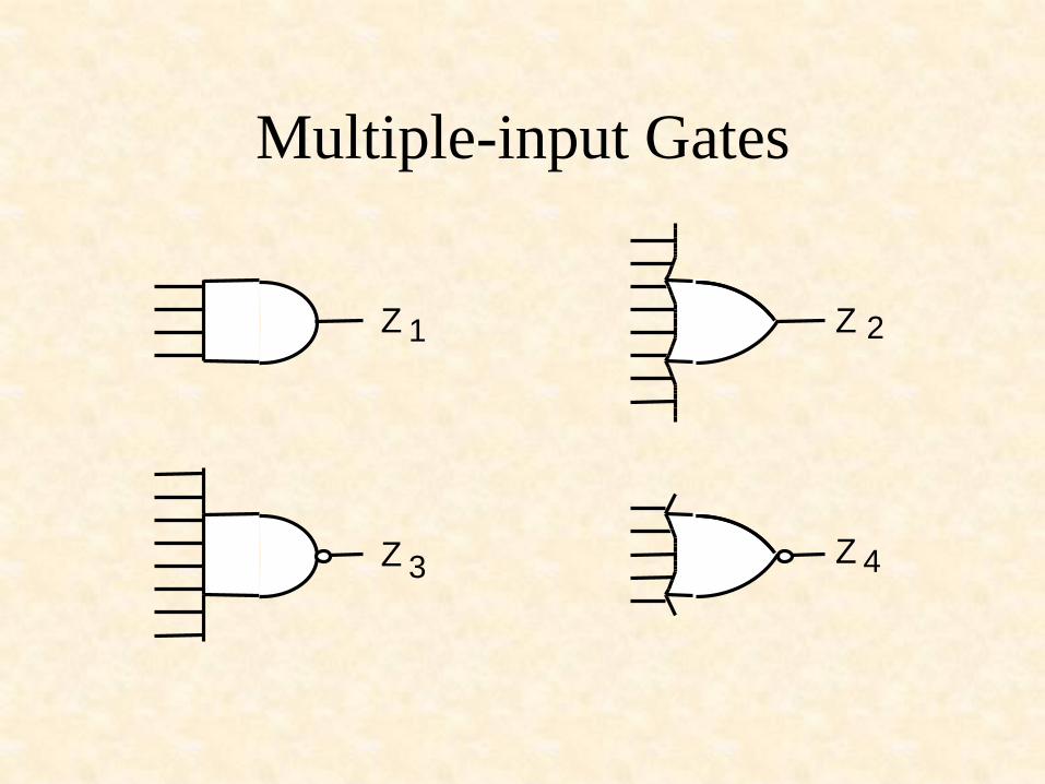
Multiple-input Gates
Z 1 2
3 4 Z Z
Z
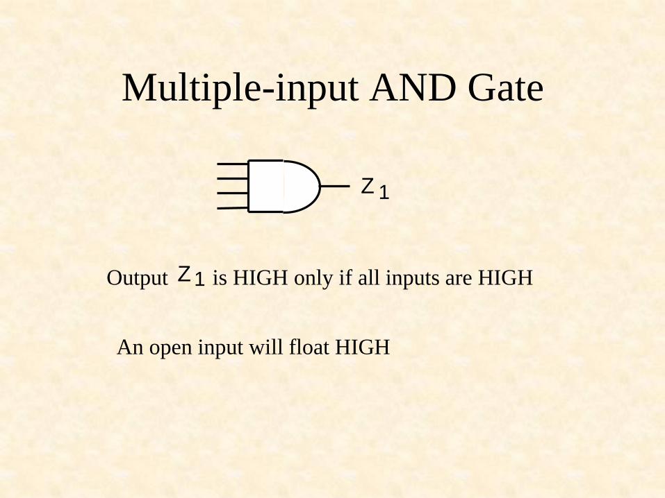
Multiple-input AND Gate
Z 1
Output is HIGH only if all inputs are HIGH Z 1
An open input will float HIGH
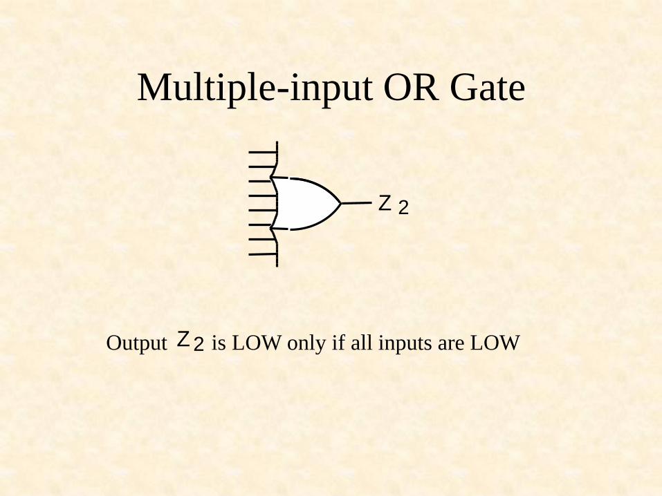
Multiple-input OR Gate
Output is LOW only if all inputs are LOW Z 2
2 Z
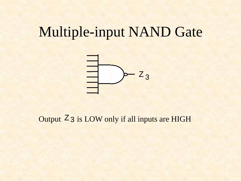
Multiple-input NAND Gate
Output is LOW only if all inputs are HIGH Z 3
3 Z
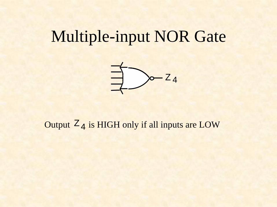
Multiple-input NOR Gate
Output is HIGH only if all inputs are LOW Z 4
4 Z
Additional Gates and Circuits – 1
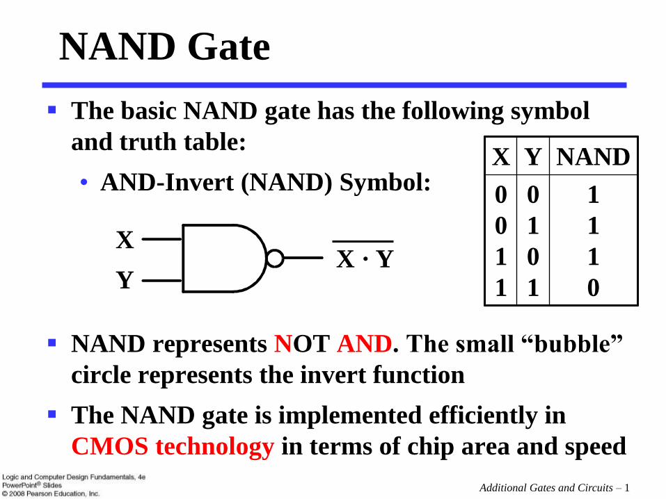
NAND Gate
The basic NAND gate has the following symbol
and truth table:
• AND-Invert (NAND) Symbol:
NAND represents NOT AND. The small “bubble”
circle represents the invert function
The NAND gate is implemented efficiently in
CMOS technology in terms of chip area and speed
X
Y X · Y
X Y NAND
0
0
1
1
0
1
0
1
1
1
1
0
Additional Gates and Circuits – 2
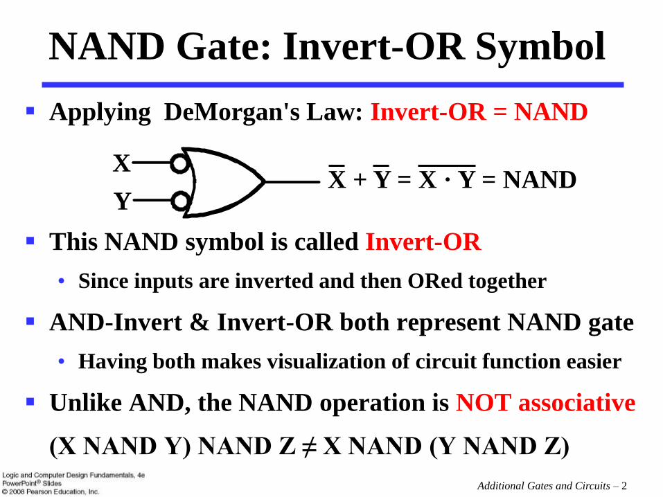
NAND Gate: Invert-OR Symbol
Applying DeMorgan's Law: Invert-OR = NAND
This NAND symbol is called Invert-OR
• Since inputs are inverted and then ORed together
AND-Invert & Invert-OR both represent NAND gate
• Having both makes visualization of circuit function easier
Unlike AND, the NAND operation is NOT associative
(X NAND Y) NAND Z ≠ X NAND (Y NAND Z)
X
Y X + Y = X · Y = NAND
Additional Gates and Circuits – 3
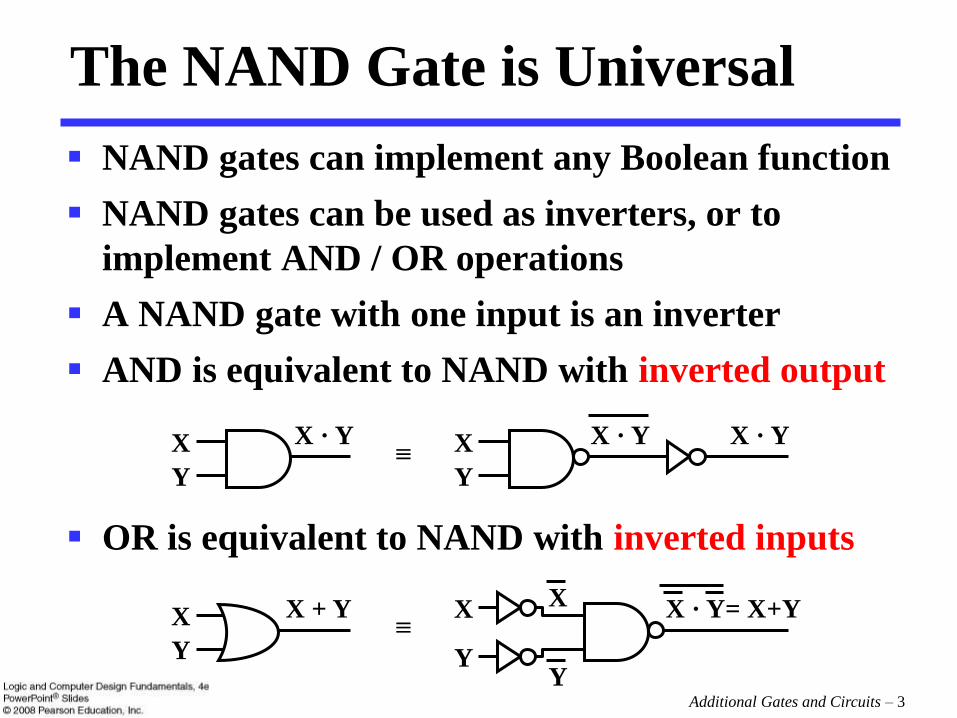
NAND gates can implement any Boolean function
NAND gates can be used as inverters, or to
implement AND / OR operations
A NAND gate with one input is an inverter
AND is equivalent to NAND with inverted output
OR is equivalent to NAND with inverted inputs
The NAND Gate is Universal
X
Y
X · Y X · Y X
Y
X · Y ≡
X · Y= X+Y X
Y
X + Y ≡
X
Y
X
Y
Additional Gates and Circuits – 4
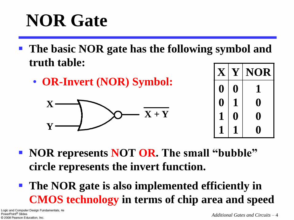
NOR Gate
The basic NOR gate has the following symbol and
truth table:
• OR-Invert (NOR) Symbol:
NOR represents NOT OR. The small “bubble”
circle represents the invert function.
The NOR gate is also implemented efficiently in
CMOS technology in terms of chip area and speed
X
Y
X + Y
X Y NOR
0
0
1
1
0
1
0
1
1
0
0
0
Additional Gates and Circuits – 5
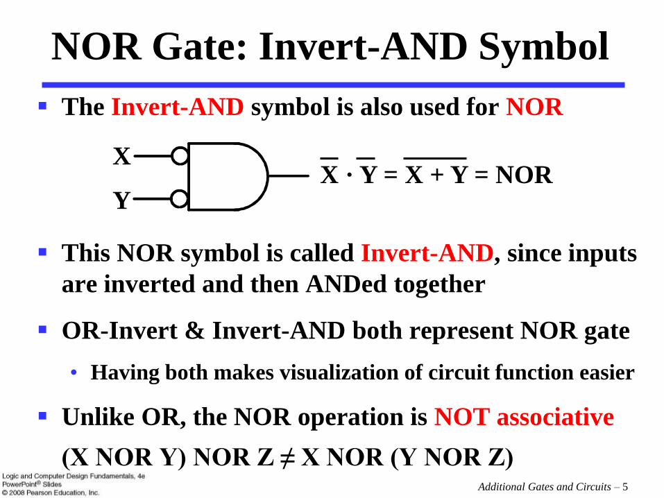
NOR Gate: Invert-AND Symbol
The Invert-AND symbol is also used for NOR
This NOR symbol is called Invert-AND, since inputs
are inverted and then ANDed together
OR-Invert & Invert-AND both represent NOR gate
• Having both makes visualization of circuit function easier
Unlike OR, the NOR operation is NOT associative
(X NOR Y) NOR Z ≠ X NOR (Y NOR Z)
X
Y X · Y = X + Y = NOR
Additional Gates and Circuits – 6
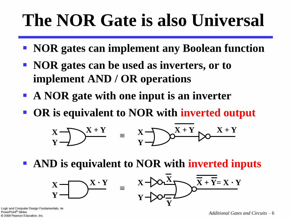
The NOR Gate is also Universal
NOR gates can implement any Boolean function
NOR gates can be used as inverters, or to
implement AND / OR operations
A NOR gate with one input is an inverter
OR is equivalent to NOR with inverted output
AND is equivalent to NOR with inverted inputs
X
Y
X + Y X + Y X
Y
X + Y ≡
X
Y
X
Y
X + Y= X · Y X
Y
X · Y ≡
Additional Gates and Circuits – 7
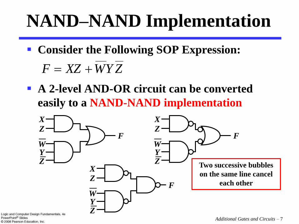
NAND–NAND Implementation
Consider the Following SOP Expression:
A 2-level AND-OR circuit can be converted
easily to a NAND-NAND implementation
ZYWXZF
X
Z
W
Z Y
F
X
Z
W
Z Y
F
Two successive bubbles
on the same line cancel
each other
X
Z
W
Z Y
F
Additional Gates and Circuits – 8
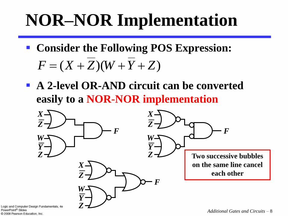
NOR–NOR Implementation
Consider the Following POS Expression:
A 2-level OR-AND circuit can be converted
easily to a NOR-NOR implementation
))(( ZYWZXF
Two successive bubbles
on the same line cancel
each other
X
Z
W
Z Y
F
X
Z
W
Z Y
F
X
Z
W
Z Y
F
Additional Gates and Circuits – 9
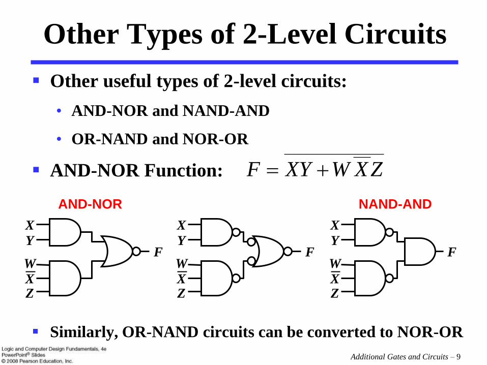
Other Types of 2-Level Circuits
Other useful types of 2-level circuits:
• AND-NOR and NAND-AND
• OR-NAND and NOR-OR
AND-NOR Function:
Similarly, OR-NAND circuits can be converted to NOR-OR
ZXWXYF
X
Y
W
Z X
F
X
Y
W
Z X
F
NAND-AND
X
Y
W
Z X
F
AND-NOR
Additional Gates and Circuits – 10
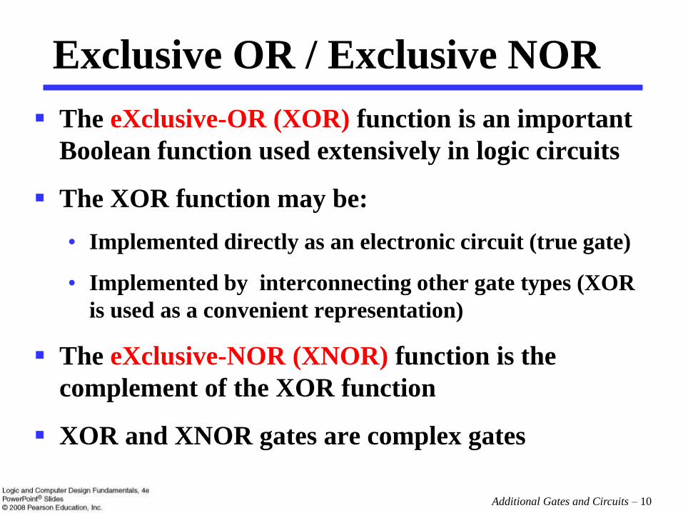
Exclusive OR / Exclusive NOR
The eXclusive-OR (XOR) function is an important
Boolean function used extensively in logic circuits
The XOR function may be:
• Implemented directly as an electronic circuit (true gate)
• Implemented by interconnecting other gate types (XOR
is used as a convenient representation)
The eXclusive-NOR (XNOR) function is the
complement of the XOR function
XOR and XNOR gates are complex gates
Additional Gates and Circuits – 11
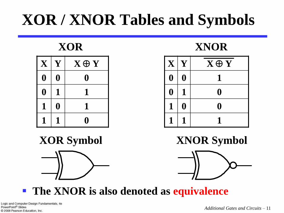
XOR / XNOR Tables and Symbols
The XNOR is also denoted as equivalence
XOR XNOR
X Y X Y
0 0 0
0 1 1
1 0 1
1 1 0
X Y X Y
0 0 1
0 1 0
1 0 0
1 1 1
XOR Symbol XNOR Symbol

Additional Gates and Circuits – 12
Uses for XOR / XNOR
SOP Expressions for XOR/XNOR:
• The XOR function is:
• The eXclusive NOR (XNOR) function, know also as
equivalence is:
Uses for the XOR and XNORs gate include:
• Adders/subtractors/multipliers
• Counters/incrementers/decrementers
• Parity generators/checkers
Strictly speaking, XOR and XNOR gates do no
exist for more that two inputs. Instead, they are
replaced by odd and even functions.
Y X Y X Y X
Y X Y X Y X
Additional Gates and Circuits – 13
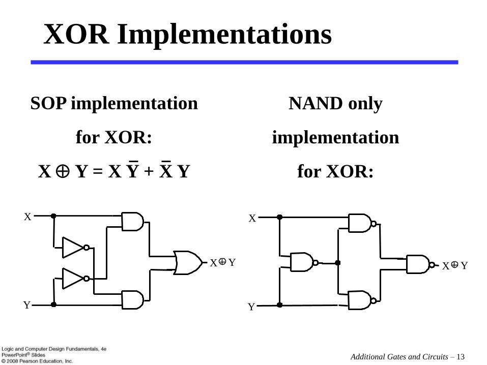
XOR Implementations
X Y
X
Y
X
Y
X Y
SOP implementation
for XOR:
X Y = X Y + X Y
NAND only
implementation
for XOR:
Additional Gates and Circuits – 14
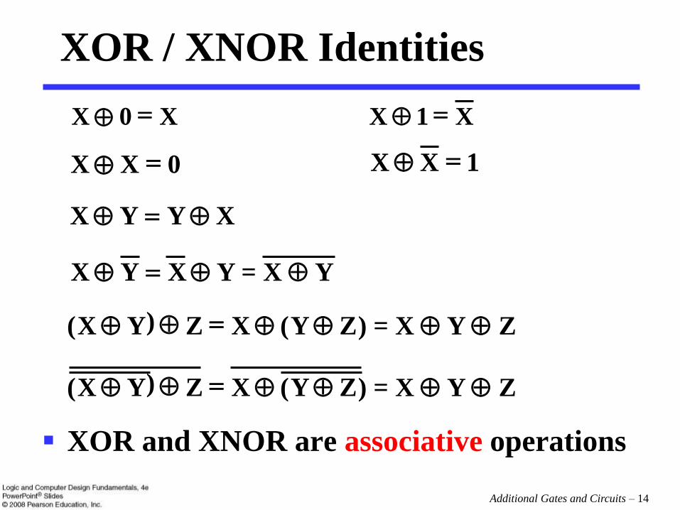
XOR / XNOR Identities
XOR and XNOR are associative operations
X 0 X X 1 X
1 X X 0 X X
X Y Y X
) = X Y Z Z Y ( X Z ) Y X (
Y = X Y X Y X
) = X Y Z Z Y ( X Z ) Y X (
Additional Gates and Circuits – 15
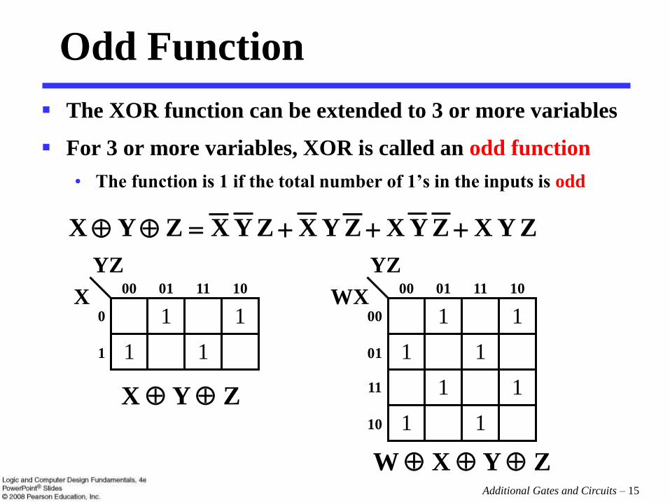
Odd Function
The XOR function can be extended to 3 or more variables
For 3 or more variables, XOR is called an odd function
• The function is 1 if the total number of 1’s in the inputs is odd
Z Y X Z Y X Z Y X Z Y X Z Y X
1 1
1 1
YZ
X 00 01 11 10
0
1
1 1
1 1
YZ
WX 00 01 11 10
00
01
1 1
1 1
11
10
X Y Z
W X Y Z
Additional Gates and Circuits – 16
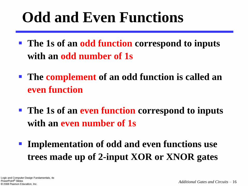
Odd and Even Functions
The 1s of an odd function correspond to inputs
with an odd number of 1s
The complement of an odd function is called an
even function
The 1s of an even function correspond to inputs
with an even number of 1s
Implementation of odd and even functions use
trees made up of 2-input XOR or XNOR gates
Additional Gates and Circuits – 17
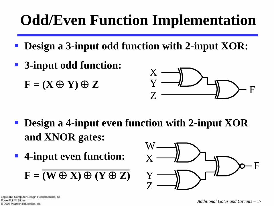
Odd/Even Function Implementation
Design a 3-input odd function with 2-input XOR:
3-input odd function:
F = (X Y) Z
Design a 4-input even function with 2-input XOR
and XNOR gates:
4-input even function:
F = (W X) (Y Z)
X Y
Z F
W
X
Y F
Z
Additional Gates and Circuits – 18
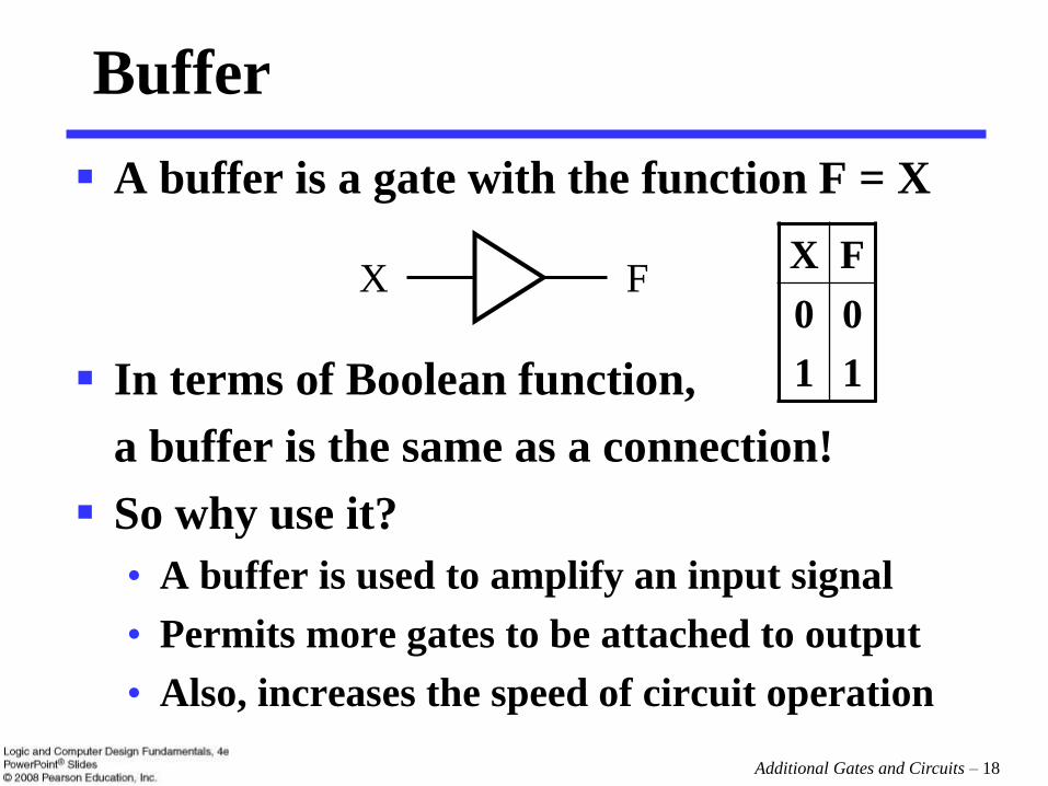
Buffer
A buffer is a gate with the function F = X
In terms of Boolean function,
a buffer is the same as a connection!
So why use it?
• A buffer is used to amplify an input signal
• Permits more gates to be attached to output
• Also, increases the speed of circuit operation
X F X F
0
1
0
1
SOP and POS Implementation
1
2
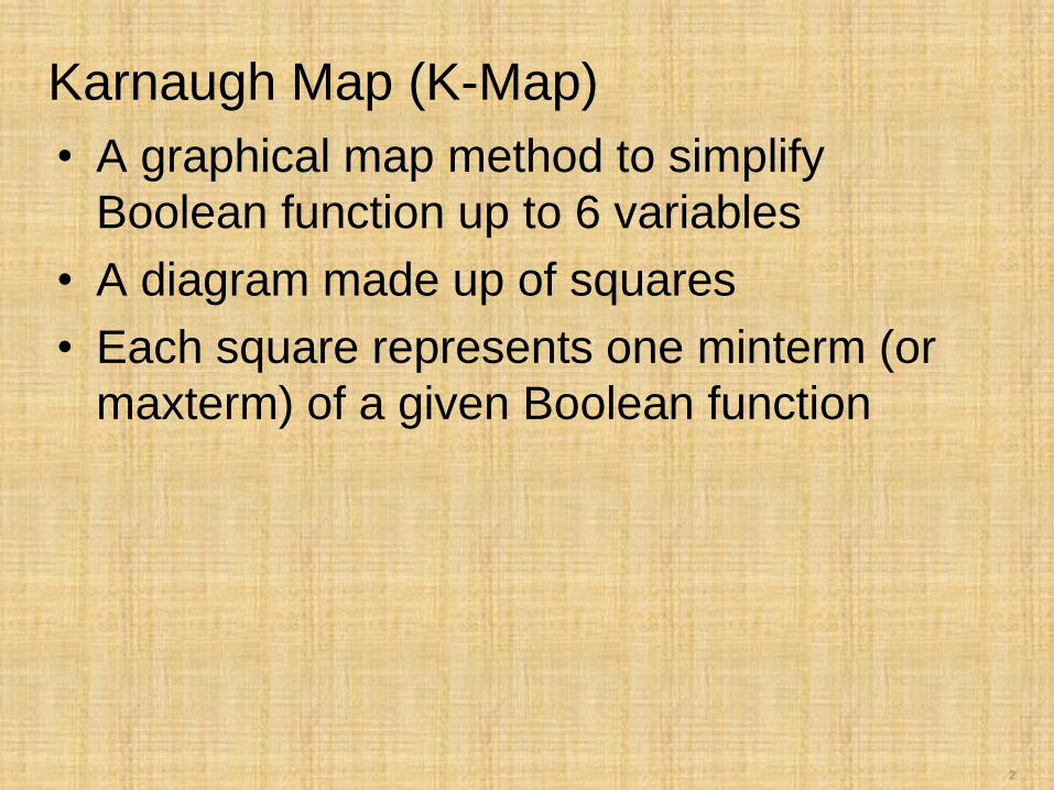
Karnaugh Map (K-Map)
• A graphical map method to simplify
Boolean function up to 6 variables
• A diagram made up of squares
• Each square represents one minterm (or
maxterm) of a given Boolean function
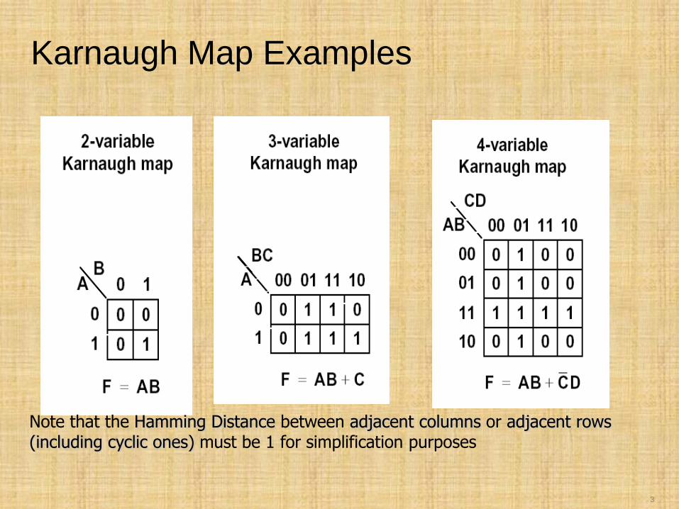
3
Karnaugh Map Examples
Note that the Hamming Distance between adjacent columns or adjacent rows (including cyclic ones) must be 1 for simplification purposes
4
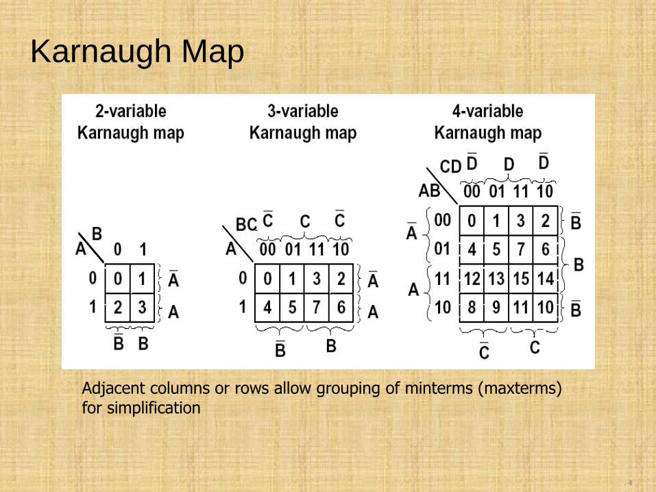
Karnaugh Map
Adjacent columns or rows allow grouping of minterms (maxterms) for simplification
5
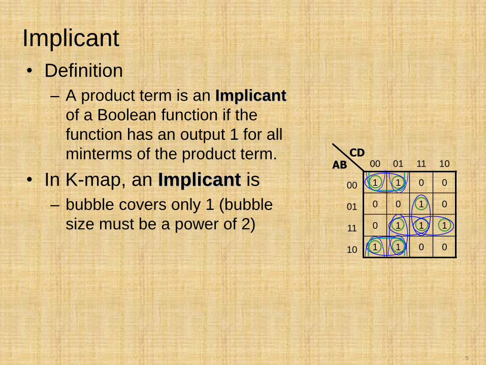
Implicant
• Definition
– A product term is an Implicant
of a Boolean function if the
function has an output 1 for all
minterms of the product term.
• In K-map, an Implicant is
– bubble covers only 1 (bubble
size must be a power of 2)
00 01 11 10
00 1 1 0 0
01 0 0 1 0
11 0 1 1 1
10 1 1 0 0
AB CD
6
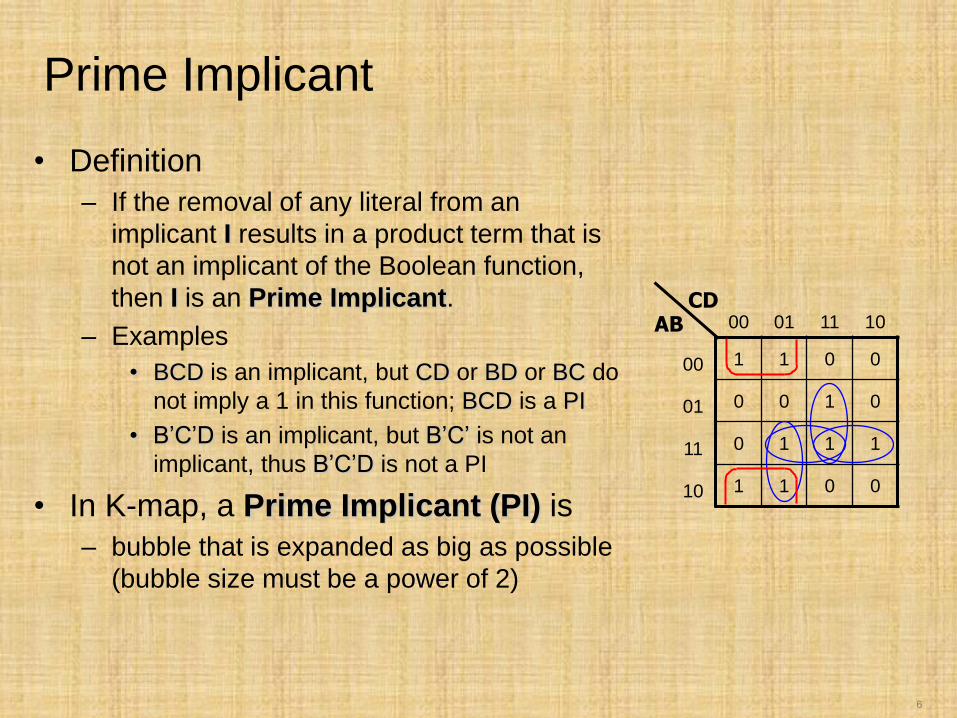
Prime Implicant
• Definition
– If the removal of any literal from an
implicant I results in a product term that is
not an implicant of the Boolean function,
then I is an Prime Implicant.
– Examples
• BCD is an implicant, but CD or BD or BC do
not imply a 1 in this function; BCD is a PI
• B’C’D is an implicant, but B’C’ is not an
implicant, thus B’C’D is not a PI
• In K-map, a Prime Implicant (PI) is
– bubble that is expanded as big as possible
(bubble size must be a power of 2)
00 01 11 10
00 1 1 0 0
01 0 0 1 0
11 0 1 1 1
10 1 1 0 0
AB CD
7
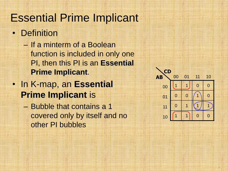
Essential Prime Implicant
• Definition
– If a minterm of a Boolean
function is included in only one
PI, then this PI is an Essential
Prime Implicant.
• In K-map, an Essential
Prime Implicant is
– Bubble that contains a 1
covered only by itself and no
other PI bubbles
00 01 11 10
00 1 1 0 0
01 0 0 1 0
11 0 1 1 1
10 1 1 0 0
AB CD
8
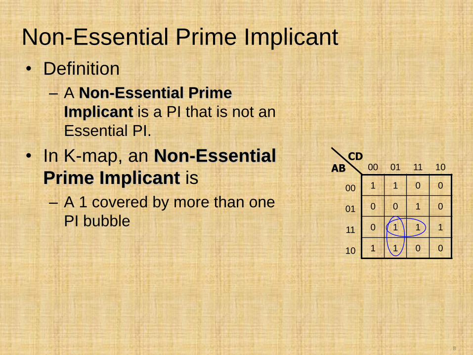
Non-Essential Prime Implicant
• Definition
– A Non-Essential Prime
Implicant is a PI that is not an
Essential PI.
• In K-map, an Non-Essential
Prime Implicant is
– A 1 covered by more than one
PI bubble
00 01 11 10
00 1 1 0 0
01 0 0 1 0
11 0 1 1 1
10 1 1 0 0
AB CD
9
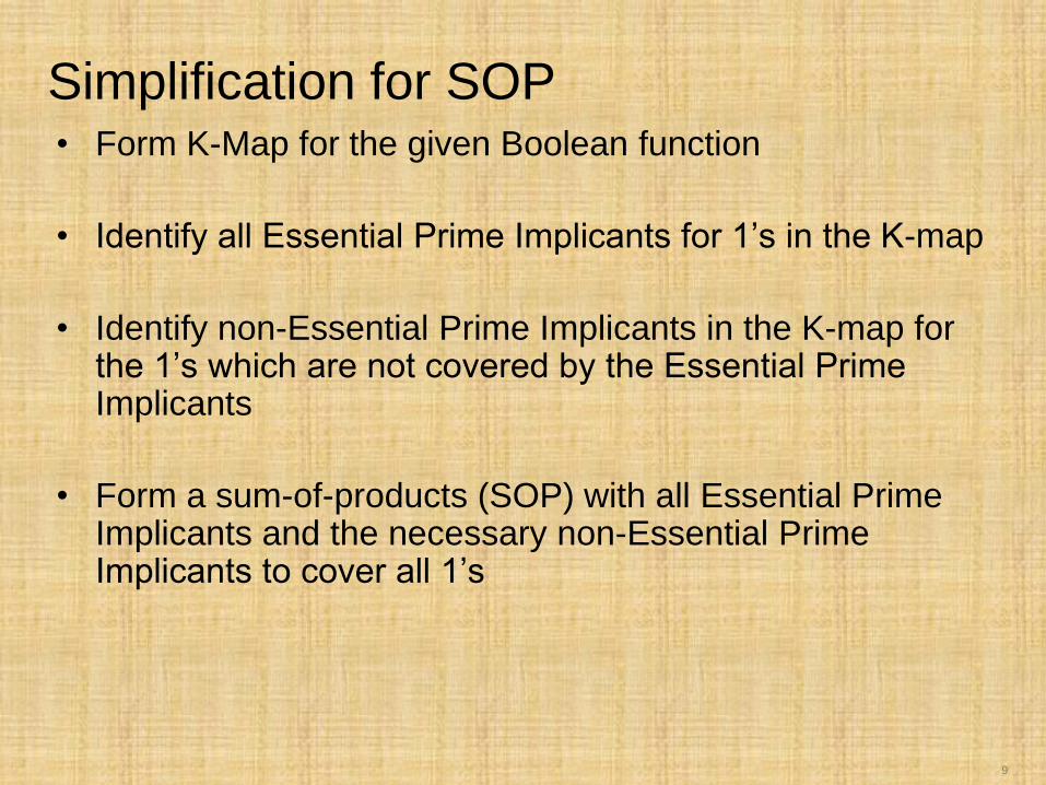
Simplification for SOP • Form K-Map for the given Boolean function
• Identify all Essential Prime Implicants for 1’s in the K-map
• Identify non-Essential Prime Implicants in the K-map for the 1’s which are not covered by the Essential Prime Implicants
• Form a sum-of-products (SOP) with all Essential Prime Implicants and the necessary non-Essential Prime Implicants to cover all 1’s
10
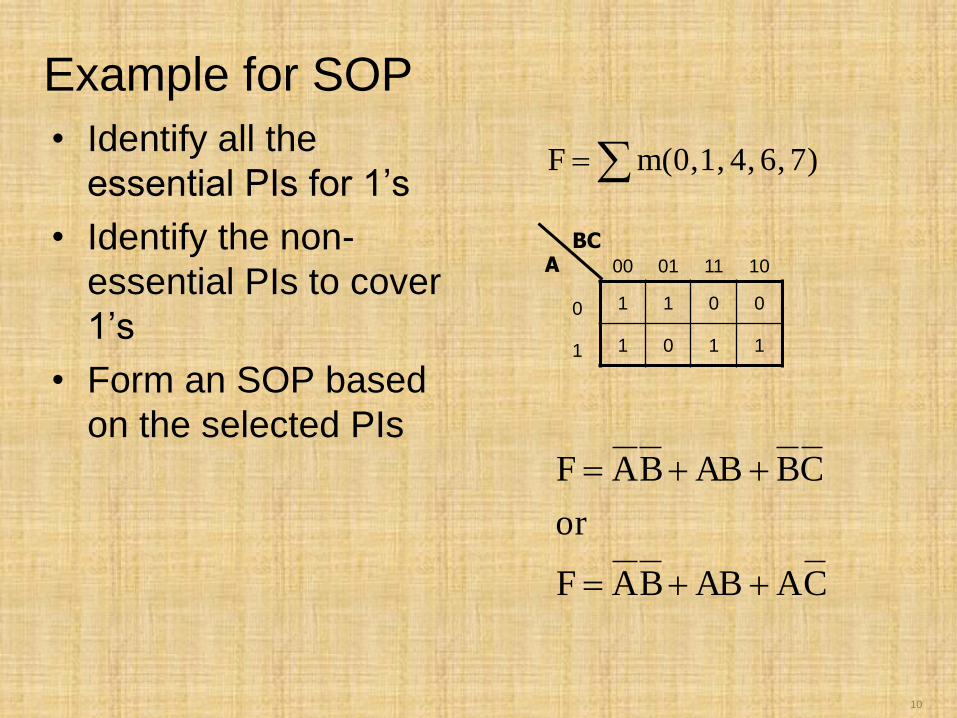
Example for SOP
• Identify all the
essential PIs for 1’s
• Identify the non-
essential PIs to cover
1’s
• Form an SOP based
on the selected PIs
7) 6, 4, 1, m(0,F
00 01 11 10
0 1 1 0 0
1 1 0 1 1
A BC
CAABBAF
or
CBABBAF
11
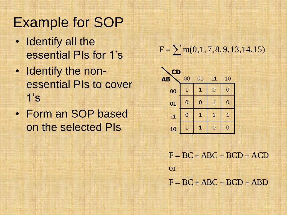
Example for SOP
• Identify all the
essential PIs for 1’s
• Identify the non-
essential PIs to cover
1’s
• Form an SOP based
on the selected PIs
15) 14, 13, 9, 8, 7, 1, m(0,F
00 01 11 10
00 1 1 0 0
01 0 0 1 0
11 0 1 1 1
10 1 1 0 0
AB CD
ABDBCDABCCBF
or
DCABCDABCCBF
12
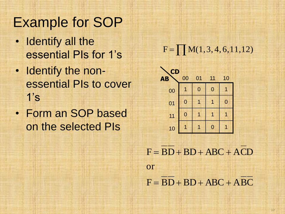
Example for SOP
• Identify all the
essential PIs for 1’s
• Identify the non-
essential PIs to cover
1’s
• Form an SOP based
on the selected PIs
12) 11, 6, 4, 3, M(1,F
00 01 11 10
00 1 0 0 1
01 0 1 1 0
11 0 1 1 1
10 1 1 0 1
AB CD
CBAABCBDDBF
or
DCAABCBDDBF
13
Prime Implicants
• All the prior definitions apply to ‘0’ (or
maxterm) as well
• Consider these implicants imply a ‘0’ output
14
Simplification for POS • Form K-Map for the given Boolean function
• Identify all Essential Prime Implicants for 0’s in the K-map
• Identify non-Essential Prime Implicants in the K-map for the 0’s which are not covered by the Essential Prime Implicants
• Form a product-of-sums (POS) with all Essential Prime Implicants and the necessary non-Essential Prime Implicants to cover all 0’s

15
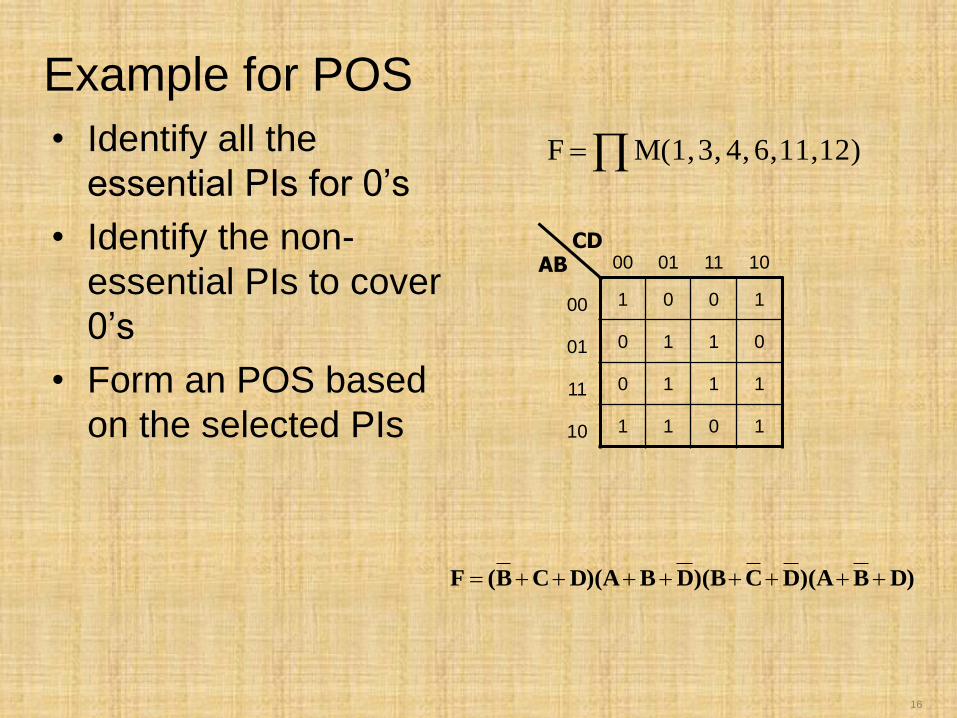
Example for POS
• Identify all the
essential PIs for 0’s
• Identify the non-
essential PIs to cover
0’s
• Form an POS based
on the selected PIs
)CBA)(B(AF
00 01 11 10
0 1 1 0 0
1 1 0 1 1
A BC
5) 3, M(2,F
16
Example for POS
• Identify all the
essential PIs for 0’s
• Identify the non-
essential PIs to cover
0’s
• Form an POS based
on the selected PIs
D)B)(ADC)(BDBD)(ACB(F
00 01 11 10
00 1 0 0 1
01 0 1 1 0
11 0 1 1 1
10 1 1 0 1
AB CD
12) 11, 6, 4, 3, M(1,F
17
Don’t Care Condition X
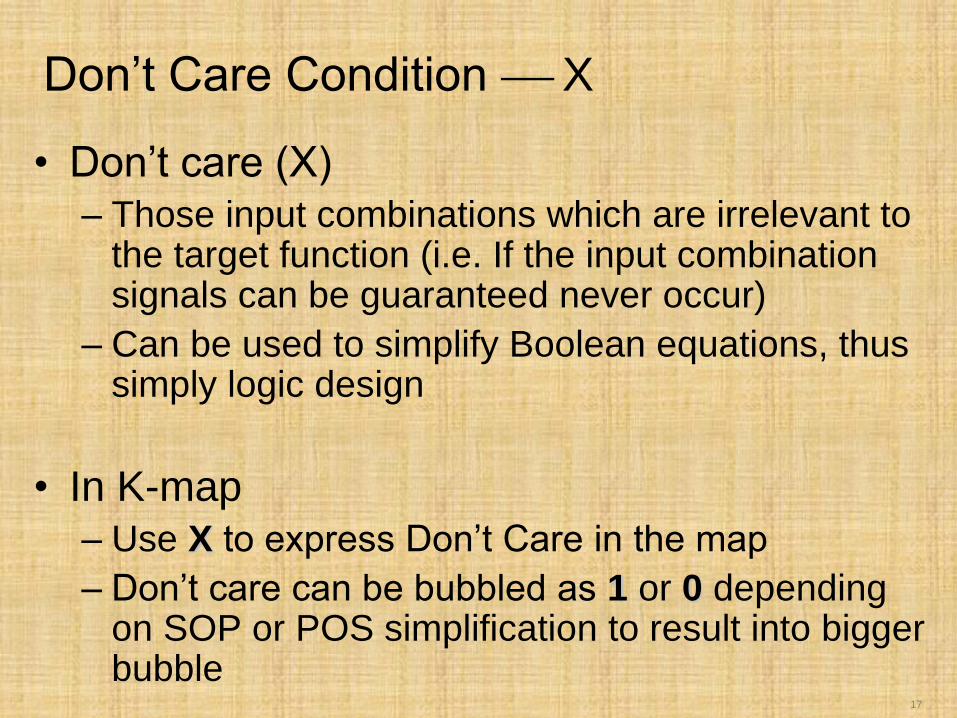
• Don’t care (X)
– Those input combinations which are irrelevant to the target function (i.e. If the input combination signals can be guaranteed never occur)
– Can be used to simplify Boolean equations, thus simply logic design
• In K-map
– Use X to express Don’t Care in the map
– Don’t care can be bubbled as 1 or 0 depending on SOP or POS simplification to result into bigger bubble
18
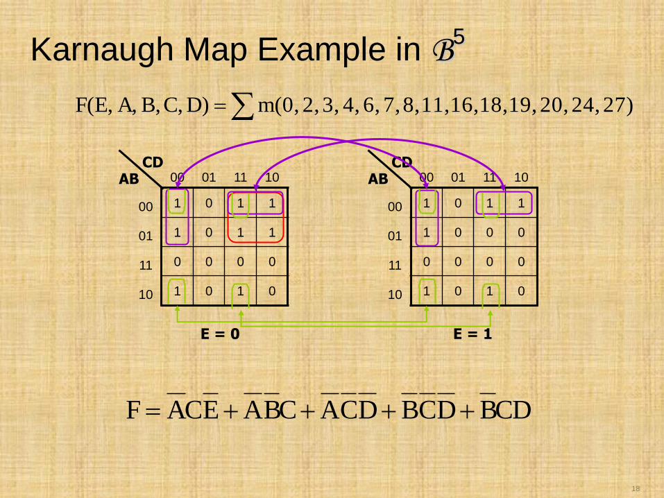
Karnaugh Map Example in B5
27) 24, 20, 19, 18, 16, 11, 8, 7, 6, 4, 3, 2, m(0,D)C,B,A, F(E,
00 01 11 10
00 1 0 1 1
01 1 0 1 1
11 0 0 0 0
10 1 0 1 0
AB CD
00 01 11 10
00 1 0 1 1
01 1 0 0 0
11 0 0 0 0
10 1 0 1 0
AB CD
E = 0 E = 1
CDBDCBDCACBAECAF
19
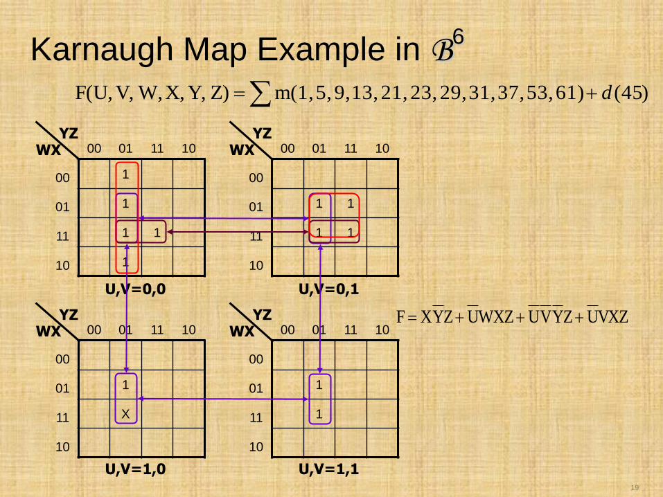
Karnaugh Map Example in B6
)45(61) 53, 37, 31, 29, 23, 21, 13, 9, 5, m(1,Z)Y,X,W,V,F(U, d
00 01 11 10
00 1
01 1
11 1 1
10 1
WX YZ
U,V=0,0
00 01 11 10
00
01 1
11 X
10
WX YZ
U,V=1,0
00 01 11 10
00
01 1 1
11 1 1
10
WX YZ
U,V=0,1
00 01 11 10
00
01 1
11 1
10
WX YZ
U,V=1,1
VXZUZYVUWXZUZYXF