1 base components of a computer 1.1 von neumann architecture€¦ · lehrstuhl für informatik 3 /...
TRANSCRIPT

Lehrstuhl für Informatik 3 / Professur für
Höchstleistungsrechnen - D. Fey / G.Wellein
Vorlesung CAMA - SS 2016
12.-26.4.2016
Department Computer Science –
Chair Computer Architecture
Dietmar Fey 1
1 Base Components of a Computer
1.1 Von Neumann Architecture
„Father“ of most computers is the classic universal computing
automaton
Basic idea postulated in a concept paper by John v.Neumann
• First Draft of a Report on the EDVAC. Moore School, University of Pennsylvania,
1945. Reprinted in IEEE Annals on the History of Computing, No. 4, 1993.
Implemented as IAS-(Institute of Advanced Studies)-Rechner
(Burks, Goldstine, John von Neumann at Princeton, 1946)
• Preliminary Discussion of the Logical Design of an Electronic computer
Instrument. Report prepared for U.S. Army Ordnance Dept., 1946, reprinted
1971.
Despite huge techological changes, the basic principle is still
found in modern microprocessors today
Lehrstuhl für Informatik 3 / Professur für
Höchstleistungsrechnen - D. Fey / G.Wellein
Vorlesung CAMA - SS 2016
12.-26.4.2016
Department Computer Science –
Chair Computer Architecture
Dietmar Fey 2
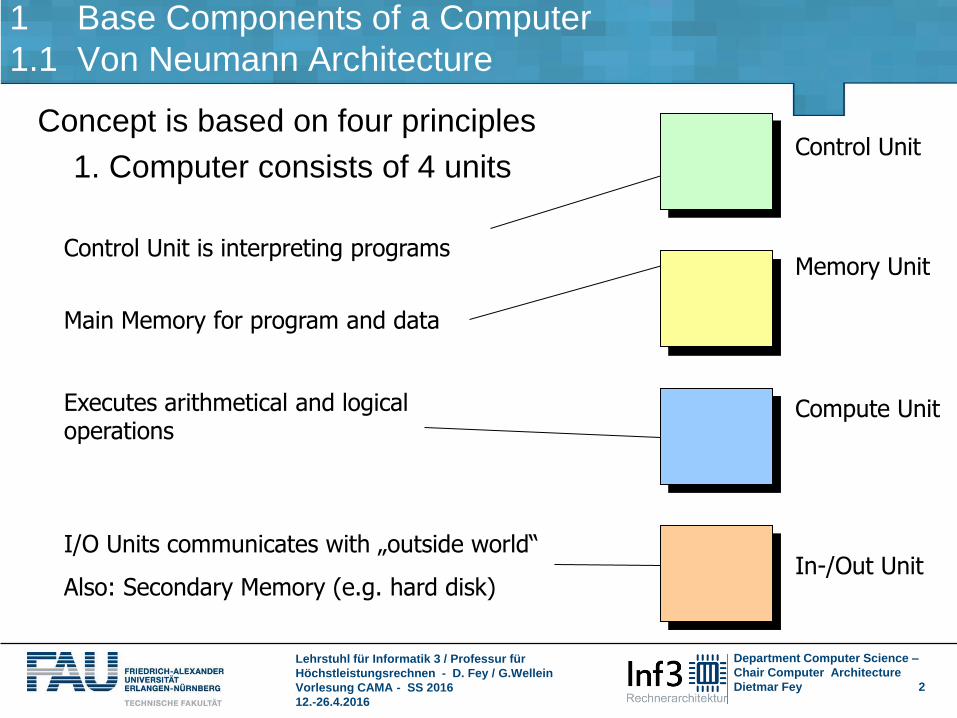
1 Base Components of a Computer
1.1 Von Neumann Architecture
Concept is based on four principles
1. Computer consists of 4 units
Compute Unit
Memory Unit
Control Unit
Control Unit is interpreting programs
Main Memory for program and data
Executes arithmetical and logical operations
I/O Units communicates with „outside world“
Also: Secondary Memory (e.g. hard disk) In-/Out Unit

Lehrstuhl für Informatik 3 / Professur für
Höchstleistungsrechnen - D. Fey / G.Wellein
Vorlesung CAMA - SS 2016
12.-26.4.2016
Department Computer Science –
Chair Computer Architecture
Dietmar Fey 3
1 Base Components of a Computer
1.1 Von Neumann Architecture
2. Computer is independent of the problem it is supposed to
solve: computer is controlled by programs
Data Result (fixed!) sequence
of arithmetical and
logical functions
HW-Programming
Controlled by program
Instruction
Interpreter
(Control Unit)
Instructions
Data Results General purpose
arithmetical and
logical functions
Control
Signals

Lehrstuhl für Informatik 3 / Professur für
Höchstleistungsrechnen - D. Fey / G.Wellein
Vorlesung CAMA - SS 2016
12.-26.4.2016
Department Computer Science –
Chair Computer Architecture
Dietmar Fey 4
1 Base Components of a Computer
1.1 Von Neumann Architecture
3. Program and data are located in the same memory. In
theory they can be modified by the computer (Note: it is
not common to modify program data during program
execution)
4. Main Memory is divided into cells of equal size and
sequentially numbered (memory address). Data and
instructions are referenced by memory addresses
5. A program consists of a sequence of instructions, which
are executed sequentially per default

Lehrstuhl für Informatik 3 / Professur für
Höchstleistungsrechnen - D. Fey / G.Wellein
Vorlesung CAMA - SS 2016
12.-26.4.2016
Department Computer Science –
Chair Computer Architecture
Dietmar Fey 5
1 Base Components of a Computer
1.1 Von Neumann Architecture
6. Exception from sequential execution of instructions by
means of conditional and unconditional branch (jump)
instructions
Causes jump to the addressed cell in main memory
Conditional branches depend on the result of arbitrary operations
7. The computer uses binary numbers

Lehrstuhl für Informatik 3 / Professur für
Höchstleistungsrechnen - D. Fey / G.Wellein
Vorlesung CAMA - SS 2016
12.-26.4.2016
Department Computer Science –
Chair Computer Architecture
Dietmar Fey 6
1 Base Components of a Computer
1.1 Components (1)
Control Unit
Microprogramming
ISA – Instruction Set Architectures
Memory and Register Addressing
Compute Unit (also: Arithmetical Logical Unit – ALU)
Integer and Floating Point Units
Memory Unit
Memory Hierarchy
Internal and External Memory Organization
I/O Unit
Communication via Networks/Busses

Lehrstuhl für Informatik 3 / Professur für
Höchstleistungsrechnen - D. Fey / G.Wellein
Vorlesung CAMA - SS 2016
12.-26.4.2016
Department Computer Science –
Chair Computer Architecture
Dietmar Fey 7
1 Base Components of a Computer
1.1.1 Microprogramming (1)
Microprogram
Mentioned for the first time by M.V. Wilkes (early 1950s)
Core of an von Neumann Architecture
Breakthrough 1964 (IBM System/360)
Why microprograms?
Semantic gap
Memory was rare and expensive in the early days
Flexibility
Microprograms
Sequence of micro instructions

Lehrstuhl für Informatik 3 / Professur für
Höchstleistungsrechnen - D. Fey / G.Wellein
Vorlesung CAMA - SS 2016
12.-26.4.2016
Department Computer Science –
Chair Computer Architecture
Dietmar Fey 8
1 Base Components of a Computer
1.1.1 Microprogramming (2)
Microprogram vs. computer program
To avoid confusion with nomenclature
• Programming of computer through Instructions
– Assembly instructions (add, sub, mul), to distinguish them from
microinstructions, we call call them macroinstructions
• Microprogramming of a computer via firmware
– Firmware = Set of all Microprograms
– Microprogram = Sequence of Microinstructions
• One assembly/(macro)instruction is mapped onto a microprogram,
which is made up of several microinstructions

Lehrstuhl für Informatik 3 / Professur für
Höchstleistungsrechnen - D. Fey / G.Wellein
Vorlesung CAMA - SS 2016
12.-26.4.2016
Department Computer Science –
Chair Computer Architecture
Dietmar Fey 9
1 Base Components of a Computer
1.1.1 Microprogramming (3)
Relation macroinstruction – microprogram/microinstruction
Macroinstruction is an entry into a microprogram
• A microprogram can also include branches
Microprogram
Microinstr. 1
Microinstr. 2
Microinstr. 3
Microinstr. n
…
(Macro-)
Instruction

Lehrstuhl für Informatik 3 / Professur für
Höchstleistungsrechnen - D. Fey / G.Wellein
Vorlesung CAMA - SS 2016
12.-26.4.2016
Department Computer Science –
Chair Computer Architecture
Dietmar Fey 10
1 Base Components of a Computer
1.1.1 Microprogramming (4)
Question: How is a (macro-)program mapped onto a
semantically equivalent series of microprograms?

Lehrstuhl für Informatik 3 / Professur für
Höchstleistungsrechnen - D. Fey / G.Wellein
Vorlesung CAMA - SS 2016
12.-26.4.2016
Department Computer Science –
Chair Computer Architecture
Dietmar Fey 11
Co
ntr
ol
Un
it
1 Base Components of a Computer
1.1.1 Microprogramming (5)
A control and a compute unit is required
Load B
Load A
0
1
A + B
A - B
B - A A
2
3
4
5
Load C
Select Adder
Select Input
Select Memory
Load D
6
7
8
9
10
Select C
Select D
12
13
From Memory
B
A
C
D
E
Adder
Input
To Memory
Output
14
Load E
Select Memory
Select Output
11
15

Lehrstuhl für Informatik 3 / Professur für
Höchstleistungsrechnen - D. Fey / G.Wellein
Vorlesung CAMA - SS 2016
12.-26.4.2016
Department Computer Science –
Chair Computer Architecture
Dietmar Fey 12
1 Base Components of a Computer
1.1.1 Microprogramming (6)
Execution of the following macroinstruction
Which microinstructions are necessary?
Which control signals must be set?
A – B → A
0 1 2 3 4 5 6 7 8 9 10 11 12 13 14 15
Lo
ad
B
Lo
ad
A
A+
B
A-B
B-A
A
Lo
ad
C
Se
lect A
dd
er
Se
let In
pu
t
Se
lect M
em
ory
Lo
ad
D
Lo
ad
E
Se
lect C
Se
ce
lt D
Se
lect M
em
ory
Se
lect O
utp
ut
0 0 0 1 0 0 1 0 0 0 0 0 0 0 0 0
0 1 0 0 0 0 0 0 0 0 0 0 1 0 0 0
Micro-
Instructions
Load A-B -> C; go to
Microinstruction 2
Load C -> A; go to
Microinstruction 3

Lehrstuhl für Informatik 3 / Professur für
Höchstleistungsrechnen - D. Fey / G.Wellein
Vorlesung CAMA - SS 2016
12.-26.4.2016
Department Computer Science –
Chair Computer Architecture
Dietmar Fey 13
1 Base Components of a Computer
1.1.1 Microprogramming (7)
What about branches?
cf. Slide 10; Instruction 19
Control unit has to be extended
Address of next instruction in F
Jump if C < 0
F
17 Sign bit of C
Adder
+1

Lehrstuhl für Informatik 3 / Professur für
Höchstleistungsrechnen - D. Fey / G.Wellein
Vorlesung CAMA - SS 2016
12.-26.4.2016
Department Computer Science –
Chair Computer Architecture
Dietmar Fey 14
1 Base Components of a Computer
1.1.1 Microprogramming (8)
Extention in detail:
C < 0 → sign bit C = ‚1‘
C ≥ 0 → sign bit C = ‚0‘
if (C < 0)
then F = F + 1 + 1
else F = F + 1 + 0 ;
Equivalent to
F = F + 1 + sign bit C
Jump
if C < 0
Address of next
micro instruction F
17
Sign bit of C
Adder
+1

Lehrstuhl für Informatik 3 / Professur für
Höchstleistungsrechnen - D. Fey / G.Wellein
Vorlesung CAMA - SS 2016
12.-26.4.2016
Department Computer Science –
Chair Computer Architecture
Dietmar Fey 15
1 Base Components of a Computer
1.1.1 Microprogramming (9)
Micro instruction sequence with branch
1 2 3 4 5 6 7 8 9 10 11 12 13 14 15 16 17
Lo
ad
B
Lo
ad
A
A+
B
A-B
B-A
A
Lo
ad
C
Se
lect A
dd
er
Se
lect In
pu
t
Se
lect M
em
ory
Lo
ad
D
Lo
ad
E
Se
lect C
Se
lect D
Se
lect M
em
ory
Se
lect O
utp
ut
Ju
mp
, if C <
0
0 0 0 1 0 0 1 1 0 0 1 0 0 0 0 0 0
0 0 0 0 0 0 0 0 0 0 0 0 0 0 0 0 1
0 0 0 0 0 0 0 0 0 0 0 1 0 1 0 0 0
A-B -> C and D;
goto microinstruction 2
if C < 0;
goto microinstruction 4
D -> E;
goto microinstruction 4
…
Micro
instruct-
tions
1
2
3
4
Lehrstuhl für Informatik 3 / Professur für
Höchstleistungsrechnen - D. Fey / G.Wellein
Vorlesung CAMA - SS 2016
12.-26.4.2016
Department Computer Science –
Chair Computer Architecture
Dietmar Fey 16
1 Base Components of a Computer
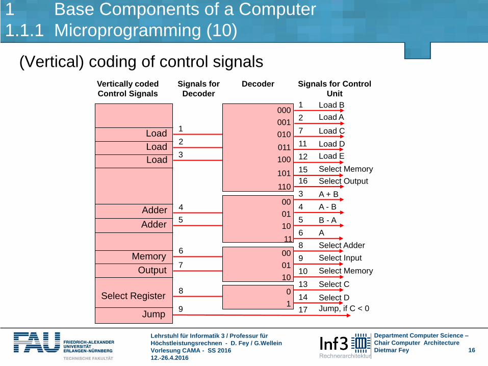
1.1.1 Microprogramming (10)
(Vertical) coding of control signals
Load
Load
Load
Adder
Adder
Memory
Output
Select Register
Jump
1
2
3
4
5
6
7
8
9
000
001
010
011
100
101
110
00
01
10
11
00
01
10
0
1
8
1
2
7
11
12
15
16
3
4
5
6
9
10
13
14
17
Load B
Load A
Load C
Load D
Load E
Select Memory
Select Output
A + B
A - B
B - A
A
Select Adder
Select Input
Select Memory
Select C
Select D
Jump, if C < 0
Vertically coded
Control Signals
Signals for
Decoder
Decoder Signals for Control
Unit
Lehrstuhl für Informatik 3 / Professur für
Höchstleistungsrechnen - D. Fey / G.Wellein
Vorlesung CAMA - SS 2016
12.-26.4.2016
Department Computer Science –
Chair Computer Architecture
Dietmar Fey 17
1 Base Components of a Computer
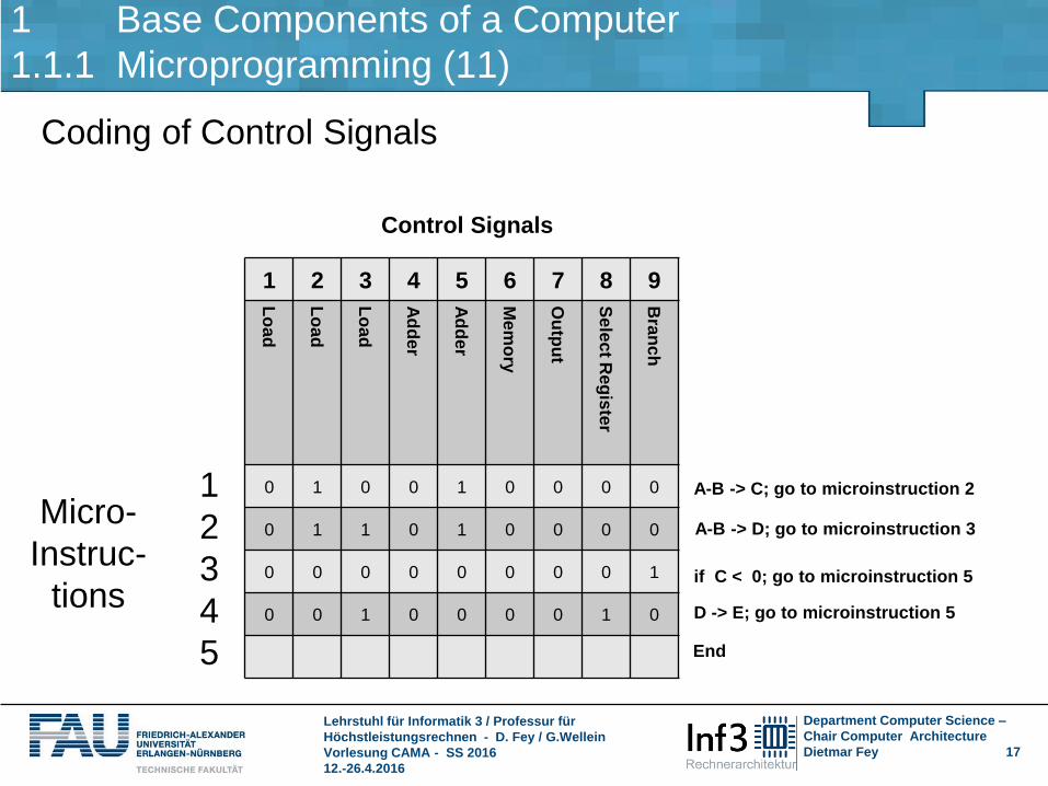
1.1.1 Microprogramming (11)
Coding of Control Signals
1 2 3 4 5 6 7 8 9
Lo
ad
Lo
ad
Lo
ad
Ad
der
Ad
der
Me
mo
ry
Ou
tpu
t
Se
lec
t Reg
iste
r
Bra
nc
h
0 1 0 0 1 0 0 0 0
0 1 1 0 1 0 0 0 0
0 0 0 0 0 0 0 0 1
0 0 1 0 0 0 0 1 0
Micro-
Instruc-
tions
A-B -> C; go to microinstruction 2
if C < 0; go to microinstruction 5
D -> E; go to microinstruction 5
1
2
3
4
5
Control Signals
End
A-B -> D; go to microinstruction 3

Lehrstuhl für Informatik 3 / Professur für
Höchstleistungsrechnen - D. Fey / G.Wellein
Vorlesung CAMA - SS 2016
12.-26.4.2016
Department Computer Science –
Chair Computer Architecture
Dietmar Fey 18
1 Base Components of a Computer
1.1.1 Microprogramming (12)
Structure of a micro-programmed architecture
(CAR) Control Address Register:
contains address of next instruction
(CBR) Control Buffer Register:
contains data from micro program
Sequencing Logic
• Generates Read Signals
• Decides from where to take
next address

Lehrstuhl für Informatik 3 / Professur für
Höchstleistungsrechnen - D. Fey / G.Wellein
Vorlesung CAMA - SS 2016
12.-26.4.2016
Department Computer Science –
Chair Computer Architecture
Dietmar Fey 19
1 Base Components of a Computer
1.1.1 Microprogramming (13)
Horizontal micro programming
Horizontal micro instruction extended with branch address
• System Bus: connects all components
• Internal CPU signals: wires that directly connect to the ALU and instruct
it to perform operations
• Indirect bit: indicates whether indirect addressing is used/not used

Lehrstuhl für Informatik 3 / Professur für
Höchstleistungsrechnen - D. Fey / G.Wellein
Vorlesung CAMA - SS 2016
12.-26.4.2016
Department Computer Science –
Chair Computer Architecture
Dietmar Fey 20
1 Base Components of a Computer
1.1.1 Microprogramming (14)
Vertical Microprogramming
Vertical Microinstruction with branch address
Instead of using control signals directly, a decoder, which creates
the actual micro instructions, is used
Advantage/Disadvantage
• More compact representation at the cost of additional decoder logic
Lehrstuhl für Informatik 3 / Professur für
Höchstleistungsrechnen - D. Fey / G.Wellein
Vorlesung CAMA - SS 2016
12.-26.4.2016
Department Computer Science –
Chair Computer Architecture
Dietmar Fey 21
1 Base Components of a Computer
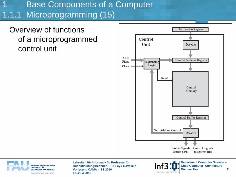
1.1.1 Microprogramming (15)
Overview of functions
of a microprogrammed
control unit

Lehrstuhl für Informatik 3 / Professur für
Höchstleistungsrechnen - D. Fey / G.Wellein
Vorlesung CAMA - SS 2016
12.-26.4.2016
Department Computer Science –
Chair Computer Architecture
Dietmar Fey 22
1 Base Components of a Computer
1.1.1 Microprogramming (16)
(External) Interrupt handling and indirect addressing
Modify instruction cycle
• Division in several states
– Fetch, Execute, Indirect Addressing, Interrupt

Lehrstuhl für Informatik 3 / Professur für
Höchstleistungsrechnen - D. Fey / G.Wellein
Vorlesung CAMA - SS 2016
12.-26.4.2016
Department Computer Science –
Chair Computer Architecture
Dietmar Fey 23
1 Base Components of a Computer
1.1.1 Microprogramming (17)
Instruction cycle (More detailed)
Takes indirect addressing and interrupts into account

Lehrstuhl für Informatik 3 / Professur für
Höchstleistungsrechnen - D. Fey / G.Wellein
Vorlesung CAMA - SS 2016
12.-26.4.2016
Department Computer Science –
Chair Computer Architecture
Dietmar Fey 24
1 Base Components of a Computer
1.1.1 Microprogramming (18)
Control unit memory
Fixed sequence of micro instruction,
which implement the previously
shown instruction cycle
• Tasks „Instruction Fetch“,
checking for „indirect addressing“
and „interrupt“ are implemented
as micro programs
• Fixed micro programs, that cannot
be changed
• Starting with AND micro program
are the instructions that implement
actual instruction
• New micro programs
(new macro instructions) can be
added by means of firmware update

Lehrstuhl für Informatik 3 / Professur für
Höchstleistungsrechnen - D. Fey / G.Wellein
Vorlesung CAMA - SS 2016
12.-26.4.2016
Department Computer Science –
Chair Computer Architecture
Dietmar Fey 25
1 Base Components of a Computer
1.1.1 Microprogramming (19)
Summary: Advantages micro programming
Micro program memory can be changed
• Leads to higher flexibility
Instruction (Set) Compatibility
• New processor can „understand“ old instructions (can be implemented
as different microprogram)
Instruction Emulation
• Processor can understand instruction set of another architecture
Idea: Don‘t use micro program memory for instruction „Translation“.
Use software instead
• Principal idea behind virtual machines

Lehrstuhl für Informatik 3 / Professur für
Höchstleistungsrechnen - D. Fey / G.Wellein
Vorlesung CAMA - SS 2016
12.-26.4.2016
Department Computer Science –
Chair Computer Architecture
Dietmar Fey 26
1 Base Components of a Computer
1.1.2 Interrupt Handling
Simplified interrupt handling
User (main) program is interrupted
and continued by another program (interrupt handler) that is excuted as
consequence of the occurred interrupt
After finishing this program
execution continues after the location where the interrupt took place

Lehrstuhl für Informatik 3 / Professur für
Höchstleistungsrechnen - D. Fey / G.Wellein
Vorlesung CAMA - SS 2016
12.-26.4.2016
Department Computer Science –
Chair Computer Architecture
Dietmar Fey 27
Re
Main Memory
CPU
P
Program
Data Register
Program Counter
A
B C
D
PC
Interrupt-Handler
Stack
0815 3141
4711 2718
Address
73
73
State before interrupt
1 Base Components of a Computer
1.1.2 Interrupt Handling

Lehrstuhl für Informatik 3 / Professur für
Höchstleistungsrechnen - D. Fey / G.Wellein
Vorlesung CAMA - SS 2016
12.-26.4.2016
Department Computer Science –
Chair Computer Architecture
Dietmar Fey 28
Re
Main Memory
CPU
P
Program
Data Register
Program Counter
A
B C
D
PC
Interrupt-Handler
Stack
0815 3141
4711 2718
Adresse
73
73
1. Incoming interrupt 2. Back up PC onto Stack 3. Load address of first instruction of interrupt handler to PC
Interrupt-Id = 158 = address
for instrcution of interrupt routine
158
1 Base Components of a Computer
1.1.2 Interrupt Handling

Lehrstuhl für Informatik 3 / Professur für
Höchstleistungsrechnen - D. Fey / G.Wellein
Vorlesung CAMA - SS 2016
12.-26.4.2016
Department Computer Science –
Chair Computer Architecture
Dietmar Fey 29
Re
CPU
Register
Program Counter
A
B C
D
PC
0815 3141
4711 2718
Adresse
158
Address of Interrupt Routine loaded into PC Main Memory
P
Program
Data
Interrupt-Handler
Stack
Adresse
73
158
1 Base Components of a Computer
1.1.2 Interrupt Handling

Lehrstuhl für Informatik 3 / Professur für
Höchstleistungsrechnen - D. Fey / G.Wellein
Vorlesung CAMA - SS 2016
12.-26.4.2016
Department Computer Science –
Chair Computer Architecture
Dietmar Fey 30
Re
Main Memory
CPU
P
Program
Data Register
Program Counter
A
B C
D
PC
Interrupt-Handler
Stack
0815 3141
4711 2718
Addresse
158
4. Back up contents of CPU registers onto stack
push B push A
push D push C
73
1 Base Components of a Computer
1.1.2 Interrupt Handling

Lehrstuhl für Informatik 3 / Professur für
Höchstleistungsrechnen - D. Fey / G.Wellein
Vorlesung CAMA - SS 2016
12.-26.4.2016
Department Computer Science –
Chair Computer Architecture
Dietmar Fey 31
Re
Main Memory
CPU
P
Program
Register
Program Counter
A B C D
PC
Interrupt-Handler
xxxx xxxx xxxx xxxx
Address 5. Complete Interrupt Routine
Data
Stack
3141 4711 2718 xxxx xxxx
… xxxx
1 Base Components of a Computer
1.1.2 Interrupt Handling

Lehrstuhl für Informatik 3 / Professur für
Höchstleistungsrechnen - D. Fey / G.Wellein
Vorlesung CAMA - SS 2016
12.-26.4.2016
Department Computer Science –
Chair Computer Architecture
Dietmar Fey 32
Re
CPU
Register
Program Counter
A
B C
D
PC
pop A
pop PC
pop C
pop B
pop D
Main Memory
P
Program
Interrupt-Handler
Data
Stack
0815 3141
4711 2718
73
1 Base Components of a Computer
1.1.2 Interrupt Handling

Lehrstuhl für Informatik 3 / Professur für
Höchstleistungsrechnen - D. Fey / G.Wellein
Vorlesung CAMA - SS 2016
12.-26.4.2016
Department Computer Science –
Chair Computer Architecture
Dietmar Fey 33
State is now the same as before interrupt
Re
Main Memory
CPU
P
Program
Data Register
Befehlszähler
A
B C
D
PC
Interrupt-Handler
Stack
0815 3141
4711 2718
Addresse
73
73
1 Base Components of a Computer
1.1.2 Interrupt Handling

Lehrstuhl für Informatik 3 / Professur für
Höchstleistungsrechnen - D. Fey / G.Wellein
Vorlesung CAMA - SS 2016
12.-26.4.2016
Department Computer Science –
Chair Computer Architecture
Dietmar Fey 34
Re
CPU
Register
Program Counter
A
B C
D
PC
0815 3141
4711 2718
74
74
7. Increment PC and continue program Main Memory
P
Program Data
Data
Interrupt-Handler
Stack
Addresse
73
1 Base Components of a Computer
1.1.2 Interrupt Handling

Lehrstuhl für Informatik 3 / Professur für
Höchstleistungsrechnen - D. Fey / G.Wellein
Vorlesung CAMA - SS 2016
12.-26.4.2016
Department Computer Science –
Chair Computer Architecture
Dietmar Fey 35
1 Base Components of a Computer
1.3 Memory (1)
Apart from the actual compute unit, the memory unit
in a computer is crucial in terms of
Performance and
Cost of a computer
Ideally
Sufficient capacity
Memory access time can keep up with processing speed of the
compute unit
Can‘t be realized due to economic and technological reasons
Solution: Memory hierarchy
Each memory level is smaller, faster, and more expensive (per byte)
than the next level
(Condition of inclusion: every memory in the hierarchy contains part
of the data from the next, higher hierarchy stage)

Lehrstuhl für Informatik 3 / Professur für
Höchstleistungsrechnen - D. Fey / G.Wellein
Vorlesung CAMA - SS 2016
12.-26.4.2016
Department Computer Science –
Chair Computer Architecture
Dietmar Fey 36
1 Base Components of a Computer
1.3.1 Memory Hierarchy (1)
Caching of data
• From main memory and registers in Cache by HW
• From background memory to main memory by SW (operating system)
Memory Acces time Capacity
Processor register 1 clock cycle 256 - 1024 Bytes
Primary cache (40:1 zu HS) 1-4 clock cycles 1 - 128 KBytes
Secondary cache (10:1 to main memory)
3-10 clock cycles 256 KB - 4 MBytes
Main memory 25-266 clock cycles ~ GBytes
Background memory 5 - 15 ms up to 5 TByte
Archive memory >> 50 ms several TBytes
Memory hierarchy and properties (approximate)

Lehrstuhl für Informatik 3 / Professur für
Höchstleistungsrechnen - D. Fey / G.Wellein
Vorlesung CAMA - SS 2016
12.-26.4.2016
Department Computer Science –
Chair Computer Architecture
Dietmar Fey 37
• Visualization of the condition of inclusion within the memory
hierarchy
Chassis
Processor
1 Base Components of a Computer
1.3.1 Memory Hierarchy (2)
Re
gis
ter
Ma
in M
em
ory
(D
RA
M)
On
-ch
ip
ca
ch
e
Primary Cache (1st level cache)
Magnedic, solid state,
optical drives
e.g. magnetic
tapes
Secondary and tertiary caches (2nd, 3rd level caches)
2nd & 3rd level
cache (SRAM)
Lehrstuhl für Informatik 3 / Professur für
Höchstleistungsrechnen - D. Fey / G.Wellein
Vorlesung CAMA - SS 2016
12.-26.4.2016
Department Computer Science –
Chair Computer Architecture
Dietmar Fey 38
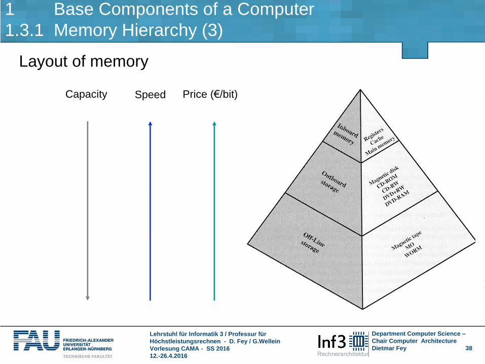
Layout of memory
Capacity Speed Price (€/bit))
1 Base Components of a Computer
1.3.1 Memory Hierarchy (3)

Lehrstuhl für Informatik 3 / Professur für
Höchstleistungsrechnen - D. Fey / G.Wellein
Vorlesung CAMA - SS 2016
12.-26.4.2016
Department Computer Science –
Chair Computer Architecture
Dietmar Fey 39
1 Base Components of a Computer
1.3.1 Memory Hierarchy (4)
Properties of memory types

Lehrstuhl für Informatik 3 / Professur für
Höchstleistungsrechnen - D. Fey / G.Wellein
Vorlesung CAMA - SS 2016
12.-26.4.2016
Department Computer Science –
Chair Computer Architecture
Dietmar Fey 40
1 Base Components of a Computer
1.3.2 Memory Structure (1)
Layout of Memory System
• Chipset (Explained later, c.f. Slide 65)

Lehrstuhl für Informatik 3 / Professur für
Höchstleistungsrechnen - D. Fey / G.Wellein
Vorlesung CAMA - SS 2016
12.-26.4.2016
Department Computer Science –
Chair Computer Architecture
Dietmar Fey 41
1 Base Components of a Computer
1.3.2 Memory Structure (2)
Processor mostly accesses fast memory (caches)
Possible due to the temporal and spatial locality of data and
instructions
0 2n - 1
Probability of
access over time
Address space

Lehrstuhl für Informatik 3 / Professur für
Höchstleistungsrechnen - D. Fey / G.Wellein
Vorlesung CAMA - SS 2016
12.-26.4.2016
Department Computer Science –
Chair Computer Architecture
Dietmar Fey 42
1 Base Components of a Computer
1.3.3 Basics of Caching (1)
Cache
Small and fast buffer memory between register file and main
memory
Purpose of a cache
Bridge the gap in performance of processor and main memory
• Processor computes data much faster than main memory delivers it
Cache organized in blocks (just like main memory)
Mostly cache lines of size 64B (Intel, AMD) or 128B (IBM POWER)

Lehrstuhl für Informatik 3 / Professur für
Höchstleistungsrechnen - D. Fey / G.Wellein
Vorlesung CAMA - SS 2016
12.-26.4.2016
Department Computer Science –
Chair Computer Architecture
Dietmar Fey 43
1 Base Components of a Computer
1.4 Main Memory Design
Main memory
Today typically made from DRAM (dynamic RAM)
Caches are typically built from SRAM (static RAM)
SRAM chips Memory cell: Flip-Flop
• Non-destructive reading possible
• Bigger than DRAM cell: 6-8 Transistors
• faster: ~ factor 8
• Lower capacity: ~ factor 8
Lehrstuhl für Informatik 3 / Professur für
Höchstleistungsrechnen - D. Fey / G.Wellein
Vorlesung CAMA - SS 2016
12.-26.4.2016
Department Computer Science –
Chair Computer Architecture
Dietmar Fey 44
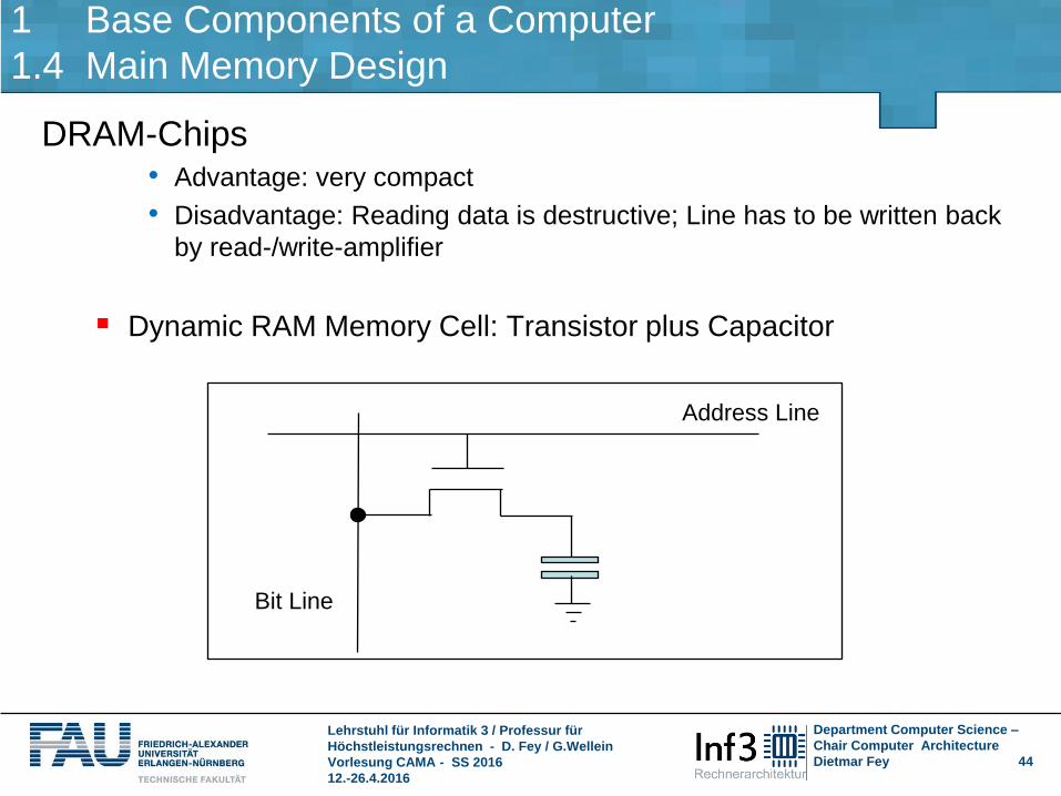
1 Base Components of a Computer
1.4 Main Memory Design
DRAM-Chips • Advantage: very compact
• Disadvantage: Reading data is destructive; Line has to be written back
by read-/write-amplifier
Dynamic RAM Memory Cell: Transistor plus Capacitor
Address Line
Bit Line

Lehrstuhl für Informatik 3 / Professur für
Höchstleistungsrechnen - D. Fey / G.Wellein
Vorlesung CAMA - SS 2016
12.-26.4.2016
Department Computer Science –
Chair Computer Architecture
Dietmar Fey 45
1 Base Components of a Computer
1.4 Main Memory Design
Main memory is made up of memory matrices
Memory matrix
with one or multiple 1-bit cells at nodes
Addressing via row and column multiplexing
• Read whole line via row address
• Addressing of bit/bits via column address
Due to leakage currents, every line has to be refreshed (rewritten) at
intervals of approximately 64 ms
• This is done by reading (and an implicit write back) of the line‘s contents
• Either block-wise, i.e. all line entries are refreshed simultaneously; or
• Entries are refreshed individually using a fixed address pattern between
the regular memory accesses
Lehrstuhl für Informatik 3 / Professur für
Höchstleistungsrechnen - D. Fey / G.Wellein
Vorlesung CAMA - SS 2016
12.-26.4.2016
Department Computer Science –
Chair Computer Architecture
Dietmar Fey 46
1 Base Components of a Computer
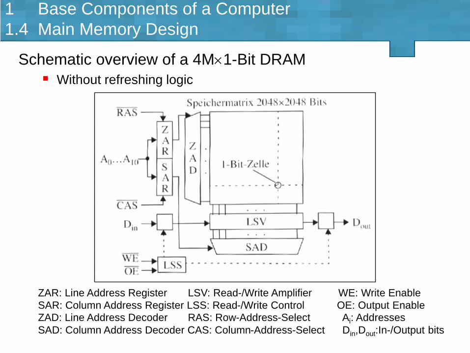
1.4 Main Memory Design
Schematic overview of a 4M1-Bit DRAM
Without refreshing logic
ZAR: Line Address Register LSV: Read-/Write Amplifier WE: Write Enable
SAR: Column Address Register LSS: Read-/Write Control OE: Output Enable
ZAD: Line Address Decoder RAS: Row-Address-Select Ai: Addresses
SAD: Column Address Decoder CAS: Column-Address-Select Din,Dout:In-/Output bits
Lehrstuhl für Informatik 3 / Professur für
Höchstleistungsrechnen - D. Fey / G.Wellein
Vorlesung CAMA - SS 2016
12.-26.4.2016
Department Computer Science –
Chair Computer Architecture
Dietmar Fey 47
1 Base Components of a Computer
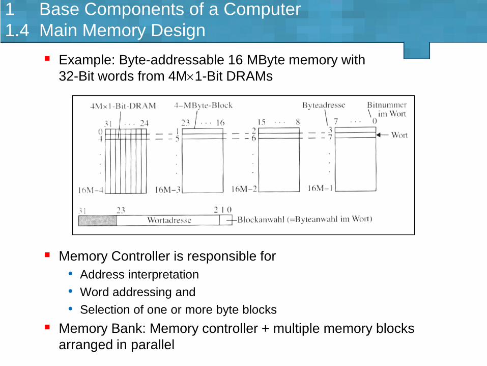
1.4 Main Memory Design
Example: Byte-addressable 16 MByte memory with
32-Bit words from 4M1-Bit DRAMs
Memory Controller is responsible for
• Address interpretation
• Word addressing and
• Selection of one or more byte blocks
Memory Bank: Memory controller + multiple memory blocks
arranged in parallel

Lehrstuhl für Informatik 3 / Professur für
Höchstleistungsrechnen - D. Fey / G.Wellein
Vorlesung CAMA - SS 2016
12.-26.4.2016
Department Computer Science –
Chair Computer Architecture
Dietmar Fey 48
1 Base Components of a Computer
1.4 Main Memory Design
Memory interleaving
Cycle time slowing down processor
• Example: 1 GHz processor and memory cycle time of 20 ns
Processor can access memory only every 20 clock cycles
Solution: Memory interleaving
• Adjacent words are located in different memory banks
• Memory access to different memory banks can overlap
Example: 4-way interleaved memory

Lehrstuhl für Informatik 3 / Professur für
Höchstleistungsrechnen - D. Fey / G.Wellein
Vorlesung CAMA - SS 2016
12.-26.4.2016
Department Computer Science –
Chair Computer Architecture
Dietmar Fey 49
1 Base Components of a Computer
1.4 Main Memory Design
Recent developments in technology
Latency of memory saw a yearly decrease of only 10%
• This is known as the memory gap

Lehrstuhl für Informatik 3 / Professur für
Höchstleistungsrechnen - D. Fey / G.Wellein
Vorlesung CAMA - SS 2016
12.-26.4.2016
Department Computer Science –
Chair Computer Architecture
Dietmar Fey 50
1 Base Components of a Computer
1.4 Main Memory Design
To decrease latency, improvements in memory design
were necessary
• Nibble-, Page- or Static Column-Mode: reading of multiple consecutive
bits in the active line at each memory access
– e.g. EDO-RAM
• EDRAM (enhanced DRAM) or CDRAM (cached DRAM)
– Cache integrated on memory chip
• SDRAM (synchronous DRAM)
– Is operated synchronous to processor- / memory bus
– In addition: more memory matrices memory interleaving
(to enable Burst Mode: fast transmission of whole blocks)
– At 100 MHz 10 ns for successive accesses
• DDR (double data rate) – RAM
– Data transmission at rising and falling edge

Lehrstuhl für Informatik 3 / Professur für
Höchstleistungsrechnen - D. Fey / G.Wellein
Vorlesung CAMA - SS 2016
12.-26.4.2016
Department Computer Science –
Chair Computer Architecture
Dietmar Fey 51
1 Base Components of a Computer
1.4 Main Memory Design
Burst Access in SDRAM
(in detail: Stallings, Chap. 5, 191-195, Synchronous DRAM)
• Read n (four in the example) consecutive addresses at once
– Latency: 2 cycles
– Burst Length: n = 4

Lehrstuhl für Informatik 3 / Professur für
Höchstleistungsrechnen - D. Fey / G.Wellein
Vorlesung CAMA - SS 2016
12.-26.4.2016
Department Computer Science –
Chair Computer Architecture
Dietmar Fey 52
1 Base Components of a Computer
1.4 Main Memory Design
Burst access and alternating access to different memory banks
http://www.hardwareecke.de/berichte/grundlagen/dram_1.php
• Access memory banks out of phase (Precharge, Active, Write/Read)

Lehrstuhl für Informatik 3 / Professur für
Höchstleistungsrechnen - D. Fey / G.Wellein
Vorlesung CAMA - SS 2016
12.-26.4.2016
Department Computer Science –
Chair Computer Architecture
Dietmar Fey 53
1 Base Components of a Computer
1.4 Main Memory Design
Today DDR technology is state of the art
Read data by rising and falling edge
Comparison of DDR-Technologies
• SDRAM – 1 Word
synchronous to bus frequency
• DDR1-400 – 2 Words
Prefetch during rising and
falling edge:
two successive addresses are read
• DDR2-533
Four words: rising and falling
edge, doubles I/O frequency

Lehrstuhl für Informatik 3 / Professur für
Höchstleistungsrechnen - D. Fey / G.Wellein
Vorlesung CAMA - SS 2016
12.-26.4.2016
Department Computer Science –
Chair Computer Architecture
Dietmar Fey 54
1 Base Components of a Computer
1.4 Main Memory Design
Technology overview [Source: Wikipedia]
Chip Module Memory
Frequency
I/O-
Frequency ²
Effective
Frequency ³
Bandwidth
per Module
Dual-
Channel
Bandwidth
DDR-200 PC-1600 100 MHz 100 MHz 200 MHz 1,6 GB/s 3,2 GB/s
DDR-266 PC-2100 133 MHz 133 MHz 266 MHz 2,1 GB/s 4,2 GB/s
DDR-333 PC-2700 166 MHz 166 MHz 333 MHz 2,7 GB/s 5,4 GB/s
DDR-400 PC-3200 200 MHz 200 MHz 400 MHz 3,2 GB/s 6,4 GB/s
Chip Module
Memory
Frequency
I/O-
Frequency ²
Effective
Frequency ³
Bandwidth
per Module
Dual-
Channel
Bandwidth
DDR2-400 PC2-3200 100 MHz 200 MHz 400 MHz 3,2 GB/s 6,4 GB/s
DDR2-533 PC2-4200 133 MHz 266 MHz 533 MHz 4,2 GB/s 8,4 GB/s
DDR2-667 PC2-5300 166 MHz 333 MHz 667 MHz 5,3 GB/s 10,6 GB/s
DDR2-800 PC2-6400 200 MHz 400 MHz 800 MHz 6,4 GB/s 12,8 GB/s
DDR2-1066 PC2-8500 266 MHz 533 MHz 1066 MHz 8,5 GB/s 17,0 GB/s
²) Frequency of bus between memory controller and RAM
³) Doubled effective frequency due to double accesses at rising and falling clock edge

Lehrstuhl für Informatik 3 / Professur für
Höchstleistungsrechnen - D. Fey / G.Wellein
Vorlesung CAMA - SS 2016
12.-26.4.2016
Department Computer Science –
Chair Computer Architecture
Dietmar Fey 55
1 Base Components of a Computer
1.5 I/O-Logic: Introduction to the bus
Schematic Overview of the bus in a PC
Connects Periphery, Memory, CPU together
Important: Bus-Arbiter (not shown) manages communication of
components on bus
Functional Classification
Spatial Classification

Lehrstuhl für Informatik 3 / Professur für
Höchstleistungsrechnen - D. Fey / G.Wellein
Vorlesung CAMA - SS 2016
12.-26.4.2016
Department Computer Science –
Chair Computer Architecture
Dietmar Fey 56
1 Base Components of a Computer
1.5 I/O-Logic: Introduction to the bus
Alternative to Bus?
Bus: in principle, all components are connected via a single line
Network with Point-to-Point (P2P) connections and router nodes
Router-
knoten

Lehrstuhl für Informatik 3 / Professur für
Höchstleistungsrechnen - D. Fey / G.Wellein
Vorlesung CAMA - SS 2016
12.-26.4.2016
Department Computer Science –
Chair Computer Architecture
Dietmar Fey 57
1 Base Components of a Computer
1.5.1 PCI-Bus
PCI-Bus (Peripheral Component Interface)
Developed as bus system by Intel for the Pentium processor
Bus frequency synchronous to CPU frequency (max. 33/66MHz)
Bus width of 32 or 64 bit
• For 32-bit bus maximum bandwidth of 44MB/s (read) or 66MB/s (write)
Capable Burst-Mode
• Peak bandwidth increases to 133 MB/s (32-bit bus) or 266 MB/s (64-bit
bus)
Use of bridges (in principle a chipset for the PCI-Bus)
• To connect the PCI-BUS to other bus systems (e.g. PCI-to-ISA-Bridge)

Lehrstuhl für Informatik 3 / Professur für
Höchstleistungsrechnen - D. Fey / G.Wellein
Vorlesung CAMA - SS 2016
12.-26.4.2016
Department Computer Science –
Chair Computer Architecture
Dietmar Fey 58
1 Base Components of a Computer
1.5.1 PCI-Bus
Bus-Master- und Slave-Principle
• A PCI-Master can read/write data from/to main memory without using
the CPU: Direct Memory Access (DMA)-Principle
• A Slave on the other side can only be a reveicer (e.g. PCI Graphics
Card)
• Automatic configuration of PCI cards
– Configuration via ROM-BIOS
– If there is a conflict, BIOS changes interrupt channels of hardware or
disables hardware in case of errors
Lehrstuhl für Informatik 3 / Professur für
Höchstleistungsrechnen - D. Fey / G.Wellein
Vorlesung CAMA - SS 2016
12.-26.4.2016
Department Computer Science –
Chair Computer Architecture
Dietmar Fey 59
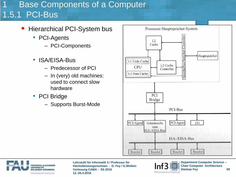
1 Base Components of a Computer
1.5.1 PCI-Bus
Hierarchical PCI-System bus
• PCI-Agents
– PCI-Components
• ISA/EISA-Bus
– Predecessor of PCI
– In (very) old machines:
used to connect slow
hardware
• PCI Bridge
– Supports Burst-Mode

Lehrstuhl für Informatik 3 / Professur für
Höchstleistungsrechnen - D. Fey / G.Wellein
Vorlesung CAMA - SS 2016
12.-26.4.2016
Department Computer Science –
Chair Computer Architecture
Dietmar Fey 60
1 Base Components of a Computer
1.5.1 PCI-Bus
Development PCI Bus

Lehrstuhl für Informatik 3 / Professur für
Höchstleistungsrechnen - D. Fey / G.Wellein
Vorlesung CAMA - SS 2016
12.-26.4.2016
Department Computer Science –
Chair Computer Architecture
Dietmar Fey 61
1 Base Components of a Computer
1.5.2 PCIe-Bus
State of the Art – PCI-Express
PCI-X bus a thing of the past
PCIe: New faster serial connections
From PCI over PCI-X to PCI-Express
• Higher Frequency
• Faster memory and slower I/O-Controller conected via data (memory)
buffer called bridge
• PCI-X had a large number of (slow) lines (82)
• PCI Express: fewer, but faster lines (P2P)
„Wir stehen vor dem radikalsten Redesign der PC-Plattform seit Einführung des PCI-Busses in den frühen 90er Jahren.“
P. Glasowsky, Microprocessor Report

Lehrstuhl für Informatik 3 / Professur für
Höchstleistungsrechnen - D. Fey / G.Wellein
Vorlesung CAMA - SS 2016
12.-26.4.2016
Department Computer Science –
Chair Computer Architecture
Dietmar Fey 62
1 Base Components of a Computer
1.5.2 PCIe-Bus
Difference PCI-(X) – PCI-Express

Lehrstuhl für Informatik 3 / Professur für
Höchstleistungsrechnen - D. Fey / G.Wellein
Vorlesung CAMA - SS 2016
12.-26.4.2016
Department Computer Science –
Chair Computer Architecture
Dietmar Fey 63
1 Base Components of a Computer
1.5.2 PCIe-Bus
Architecture – PCI-Express
Root, Switches
Links, Bridges
2,5-80 GBit/s
depending on number
of multiplexed lines

Lehrstuhl für Informatik 3 / Professur für
Höchstleistungsrechnen - D. Fey / G.Wellein
Vorlesung CAMA - SS 2016
12.-26.4.2016
Department Computer Science –
Chair Computer Architecture
Dietmar Fey 64
1 Base Components of a Computer
1.5.3 USB-Bus
USB (Universal Serial Bus)-Bus
Star-Topology
• Up to 127 devices
USB-Controller is in charge
• No direct connection between individual USB devices
• USB Controller works as host
• USB Controller is the only device that has to be assigned an interrupt line by the BIOS
Development
• In the beginning: 1,5 Mbit/s (USB 1.0) resp. 12 Mbit/s (USB 1.1)
• USB 2.0 with max. 480 MBit/s
• USB 3.0: 5.0 Gbit/s
„hot-plugging“
• Devices can be plugged in, reconnected while the computer is operating

Lehrstuhl für Informatik 3 / Professur für
Höchstleistungsrechnen - D. Fey / G.Wellein
Vorlesung CAMA - SS 2016
12.-26.4.2016
Department Computer Science –
Chair Computer Architecture
Dietmar Fey 65
1 Base Components of a Computer
1.5.3 Chipsets
Chipsets realise the interface of the
Processor-Memory-Periphery System

Lehrstuhl für Informatik 3 / Professur für
Höchstleistungsrechnen - D. Fey / G.Wellein
Vorlesung CAMA - SS 2016
12.-26.4.2016
Department Computer Science –
Chair Computer Architecture
Dietmar Fey 66
1 Base Components of a Computer
1.6 Coupling of Memory with I/O
Three fundamental modes of operation
Programmed Input/Output
Handled by the processor
Interrupt-Driven I/O
Handled by the processor when an interrupt occurs
DMA (Direct Memory Access)
• Only initiated by the processor
• DMA controller handles data transfer between main memory and
periphery without the processor

Lehrstuhl für Informatik 3 / Professur für
Höchstleistungsrechnen - D. Fey / G.Wellein
Vorlesung CAMA - SS 2016
12.-26.4.2016
Department Computer Science –
Chair Computer Architecture
Dietmar Fey 67
1 Base Components of a Computer
1.6 Coupling of Memory with I/O

Lehrstuhl für Informatik 3 / Professur für
Höchstleistungsrechnen - D. Fey / G.Wellein
Vorlesung CAMA - SS 2016
12.-26.4.2016
Department Computer Science –
Chair Computer Architecture
Dietmar Fey 68
1 Base Components of a Computer
1.6.1 Addressing of Peripheral Devices
Two addressing modes for
peripheral devices
• Mapped Memory
– Periphery is addressed via
normal memory
(the devices‘ control registers
are mapped onto addresses
in main memory)
• Isolated I/O
– Periphery is addressed by
separated instructions
(in, out vs. mov)
7 6 5 4 3 2 1 0
516 Keyboard input data register
7 6 5 4 3 2 1 0
517 Keyboard input status and
control register
(a) Example „Memory-mapped I/O
ADRESS INSTRCUTION OPERAND COMMENT
200 Load AC „1“ Load accumalator
201 Store AC 517 Initiate keyboard read
202 Load AC 517 Get status byte
203 Branch if sign = 0 202 Loop until ready
204 Load AC 516 Load data byte
(b) Example „Isolated I/O“
ADRESS INSTRCUTION OPERAND COMMENT
200 Load I/O 5 Initiate keyboard read
201 Test I/O 5 Check for completion
202 Branch Not Ready 201 Loop until ready
204 In 5 Load data byte

Lehrstuhl für Informatik 3 / Professur für
Höchstleistungsrechnen - D. Fey / G.Wellein
Vorlesung CAMA - SS 2016
12.-26.4.2016
Department Computer Science –
Chair Computer Architecture
Dietmar Fey 69
1 Base Components of a Computer
1.6.2 Interrup driven I/O
Control flow: Interrupt driven I/O
PSW: Program status word
PC: Program counter

Lehrstuhl für Informatik 3 / Professur für
Höchstleistungsrechnen - D. Fey / G.Wellein
Vorlesung CAMA - SS 2016
12.-26.4.2016
Department Computer Science –
Chair Computer Architecture
Dietmar Fey 70
1 Base Components of a Computer
1.6.3 Programmed I/O
Control flow: programmed I/O (PIO)
• CPU takes care of everything

Lehrstuhl für Informatik 3 / Professur für
Höchstleistungsrechnen - D. Fey / G.Wellein
Vorlesung CAMA - SS 2016
12.-26.4.2016
Department Computer Science –
Chair Computer Architecture
Dietmar Fey 71
1 Base Components of a Computer
1.6.4 Interrupt driven I/O vs. DMA
Interrupt driven I/O
• CPU is waiting for interrupt
• Fetches data itself
DMA
• CPU issues job to the DMA
controller
• DMA controller completes
memory transfer
• CPU is notified of completion via
interrupt by the DMA controller