08 epico2012 shibuya - icamicam-i2cam.org/images/uploads/08_epico2012_shibuya.pdf · electric...
TRANSCRIPT

Electric Pulsed Induced Changes in Oxides 2012
K. Shibuya
Phase control of bistable metal-insulator states in
vanadium dioxide
AIST

Electric Pulsed Induced Changes in Oxides 2012
Where is RIKEN and AIST?
RIKEN :the institute of physical and chemical research
Narita airport
City center
2
60km

Electric Pulsed Induced Changes in Oxides 2012
Background of vanadium dioxide
10-4
10-3
10-2
10-1
100
101
102
Res
istiv
ity (
cm
)
4003002001000
Temperature (K)
V0.91W0.09O2
VO2
Room temperature
Metal
Insulator
TMI above room temperature
Chemical substitution
Metal InsulatorTMI = 340 K
Rutile P42/mnm Monoclinic P21/C
~ 0.5 eV
3

Electric Pulsed Induced Changes in Oxides 2012
4
Sneak current TiO2
VO2
TiO2/VO2

Electric Pulsed Induced Changes in Oxides 2012
Background of vanadium dioxide
Insulator
Metal
Smart window
Tran
smitt
ance
Temperature
TMI
M. Soltani et al, J. Vac. Sci. Thechnol. A25, 971 (2005).
After AIST press lease (2005)
Photo switch
Thermochromic property
SapphireVO2
λ=1.55 µm
Thermal control Electric-field, photo, pressure control
Metal
PhotonElectric field
Winter Summer
Pressure
5

Electric Pulsed Induced Changes in Oxides 2012
Outline
1. Phase control by chemical substitution2. TiO2/VO2 superlattices3. VO2/Nb:TiO2 junctions4. Electric-field-induced phase transition5. X-ray photo-induced phase transition6. High-pressure-induced phase transition
6

Electric Pulsed Induced Changes in Oxides 2012
Overall supervisionRIKEN & U. Tokyo: M. Kawasaki & Y. Tokura
X-ray Diffraction RIKEN: D. Okuyama, Y. Taguchi, & T. ArimaKEK: Y. Yamasaki, K. Kobayashi, H. Nakao, R. Kumai, & Y. Murakami
Photoemission spectroscopyU. Tokyo: E. Sakai, K. Yoshimatsu, H. Kumigashira, & M. Oshima
Optical studyGIST: J. S. Lee
Electric Double Layer Transistor (ELDT)RIKEN: M. Nakano, T. Hatano, & Y. Iwasa
High pressure measurementRIKEN: C. Terakura
Acknowledgements
7

Electric Pulsed Induced Changes in Oxides 2012
1. Phase control by chemical substitution
8

Electric Pulsed Induced Changes in Oxides 2012
400
300
200
100
0
Tem
pera
ture
(K)
0.200.150.100.050.00
x in V1-xWxO2
-4
-2
0
2
Log(Resistivity/
cm)
Metal
Insulator Insulator
Electron-doping in VO2 thin films
K. Shibuya et al, APL 96, 022102 (2010)
Spin-singlet formation vs. kinetic energyThe dimerization is destabilized with electron-dopingV1-xWxO2 /TiO2(001)
Electron-doping can control the transition temperature and the metallic state is stabilized.
(Mott)
9

Electric Pulsed Induced Changes in Oxides 2012
Optical study for V1-xWxO2 thin films
Metal
Metal
Insulator
Insulator
Lower doping (x=0.05) Charge and lattice dynamics
J. S. Lee, K. Shibuya et al, PRB 85, 155110 (2012)
10

Electric Pulsed Induced Changes in Oxides 2012
Photoemission study for V1-xWxO2 thin films
E. Sakai, K. Shibuya et al, PRB 84, 195132 (2011)
Spin-Peierls
Mott insulator
Lower doping
Higher doping
Electron
V4+
V3+
Electron correlation
MetalInsulator
Electronic structure
W5d+O2p
11

Electric Pulsed Induced Changes in Oxides 2012
2. TiO2/VO2 superlattices
12

Electric Pulsed Induced Changes in Oxides 2012
TiO2/VO2 superlattices
3d1/3d0 interface
TiO2(001)VO2
TiO2
VO2
TiO2
VO2
TiO2
nmnmnm
Motivation:Interface properties in rutile
A superlattice of rutile-type layers (m=5)
PRL 102, 166803 (2009) Prediction:VO2 metallic ground state
13

Electric Pulsed Induced Changes in Oxides 2012
TiO2/VO2 superlattices
Structural change
Robust V-V dimerization
(TiO2)m/(VO2)n
Neither metallic nor ferromagnetic
Low temp
High temp
14

Electric Pulsed Induced Changes in Oxides 2012
Both W:VO2 and TiO2 layers are rutile.
TiO2/V0.92W0.08O2 superlattices
The revival of the insulating ground state was observed.
The inherently metallic electron-doped VO2 layer was alternatively utilized.
K. Shibuya et al, PPB 82, 205118 (2010).
15

Electric Pulsed Induced Changes in Oxides 2012
The bulk-like metallic phase is stabilized when the film thickness exceeds 6 ML.
SrVO3/SrTiO3
Photoemission study:K. Yoshimatsu et al., PRL 104, 147601 (2010).
In Perovskite
single layer
single layer
TiO2/VO2
TiO2/W:VO2
SrVO3/SrTiO3
Discussion
Spin-singlet state is favored at the interfaces due to strong electron-lattice interaction.
D. H. Kim et al., Solid State Commun. 114, 473 (2000).
16

Electric Pulsed Induced Changes in Oxides 2012
3. VO2/Nb:TiO2 junctions
17

Electric Pulsed Induced Changes in Oxides 2012
V1-xCrxO2 thin films400
350
300
250
200
150
Tem
pera
ture
(K)
0.300.250.200.150.100.050.00y in V1-yCryO2
-3
-2
-1
0
1
2
Log (Resistivity/ cm
)
Insulator
MetalThin film
Bulk
18Phys. Rev. B 8, 1323 (1973)

Electric Pulsed Induced Changes in Oxides 2012
1 2 1 1
21
′1
1
VO2/Nb:TiO2 junction
19
TiO2 VO2
No indication of depletion layer in VO2
Hole-dopingElectron-doping
Nb:0.05wt%

Electric Pulsed Induced Changes in Oxides 2012
VO2/Nb:TiO2 junction
20
VO2 work function∼ 5 eV
A. Sawa et al, APL 90, 252102 (2007)
Perovskite

Electric Pulsed Induced Changes in Oxides 2012
4. Electric-field-induced phase transition
21

Electric Pulsed Induced Changes in Oxides 2012
22
Electric-field induced phase transition
VO2
M. Nakano, K. Shibuya et al, Nature 487, 459 (2012)
a,b, A schematic (a) and an optical micrograph (b) of an EDLT with a coplanar gate electrode. A small droplet of an ionic liquid, DEME-TFSI, covers both a channel and a gate electrode so that ions can freely move between these areas back and forth depending on a gate voltage, enabling electrical switching.

Electric Pulsed Induced Changes in Oxides 2012
23
Electric-field induced phase transitionNon-volatile action
Insulator
MetalThe temperature dependence of the sheet resistivity under different VG. Once a positive gate bias is applied, the metal-insulator transition temperature decreases drastically. Above VG = 0.8 V, the sample shows almost metallic behavior.

Electric Pulsed Induced Changes in Oxides 2012
¥
Electric-field induced phase transition
M. Nakano, K. Shibuya et al, Nature 487, 459 (2012).
Gate voltage
Carrier injection by E
24

Electric Pulsed Induced Changes in Oxides 2012
5. X-ray photo-induced phase transition
25

Electric Pulsed Induced Changes in Oxides 2012PRL 87, 237401 (2001)
Optical phonon
Rutile
Monoclinic
VO2 single crystal at 300 K
Photo-induced phase transition at room temperatureBut not persistent
26
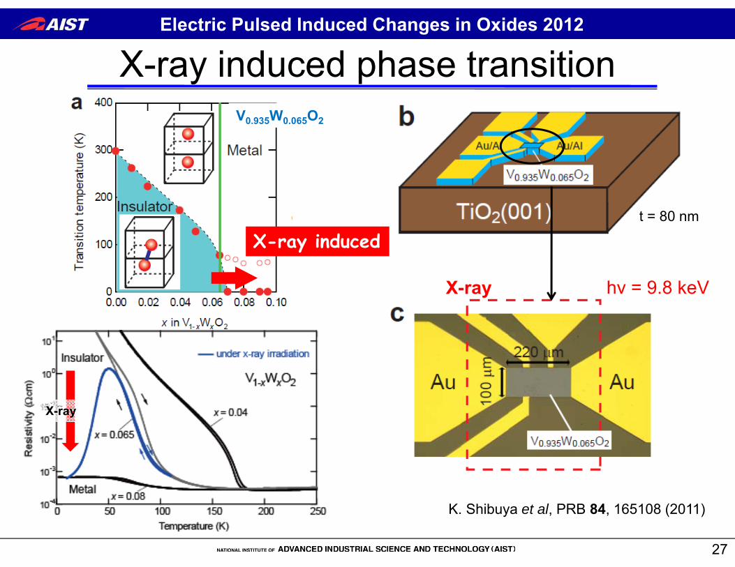
Electric Pulsed Induced Changes in Oxides 2012
X-ray induced phase transitionV0.935W0.065O2
X-ray
X-ray inducedt = 80 nm
hν = 9.8 keV
K. Shibuya et al, PRB 84, 165108 (2011)
X-ray
27

Electric Pulsed Induced Changes in Oxides 2012
A negligible relaxation process was seen without X-ray irradiation. The persistent phase transition was confirmed.
X-ray induced phase transition
XRD patterns during the phase transition
metal
insulator0 s
2000 s
Volu
me
frac
tion
of
the
met
al p
hase
Con
duct
ivity
(S/
cm)
Irradiation time (s)
T = 9 K
X-ray photon MetalInsulator
8.4 × 10¹¹ photon/cm2 s
30nm
28

Electric Pulsed Induced Changes in Oxides 2012
Flux dependence and scaling
Photon flux1012101310141015 Percolation
processfor t
he in
sula
ting
phas
e
Converted from
diffraction intensity data
scVV 0
29
The insulator-metal transition is well-scaled with the time-integrated photon density, independent of flux density.

Electric Pulsed Induced Changes in Oxides 2012
6. High-pressure-induced phase transition
30

Electric Pulsed Induced Changes in Oxides 2012
[100]M2 // [001]R
more insulating
Adv. Mater. 22, 5134 (2010).
31

Electric Pulsed Induced Changes in Oxides 2012
V0.94W0.06O2/TiO2(001)
High-pressure effect
Pressure cell
Cubic anvil systemHydrostatic pressure
t = 100 nm
0GPa
10GPa
Hydrostatic pressure induces an insulator‐metal transition.
32

Electric Pulsed Induced Changes in Oxides 2012
With use of DAC and synchrotron X-ray
X-ray diffraction under high pressure
V0.94W0.06O2/TiO2(001)
(101)Insulator
Metal
TMI
TMI
33

Electric Pulsed Induced Changes in Oxides 2012
High pressure induces a correlated metal.
Pressure
Pressure
Hall measurements for V0.933W0.067O2 under hydrostatic pressures
With use of a piston-type pressure cell
34

Electric Pulsed Induced Changes in Oxides 2012
3D phase diagram
MetalIns.
Pressure-induced insulator-metal transition was seen at the phase boundary.35

Electric Pulsed Induced Changes in Oxides 2012
Summary
MetalVO2
Structure change
Electron-doping
(External) Pressure
X-ray(Light)
YesYes
Electric field Structurestrain
Insulator
YesYes YesYes
No, so farNo, so far
The metallic state is stabilized by chemical substitution. The collective dimerization is robust even at the interfaces. Electronic phases of VO2 can be controlled by external stimuli such as electric field, X‐ray, and high‐pressure. The electronic state is closely interrelated with the lattice‐structural change. The electric‐field control is the most powerful perturbation for device application.
YesYes
36
Electron correlation&
Electron lattice coupling
Electron correlation&
Electron lattice coupling

Electric Pulsed Induced Changes in Oxides 2012
Back-up
37

Electric Pulsed Induced Changes in Oxides 2012
Y. Muraoka et al., APL 80, 583 (2002).
VO2
TiO2Lattice mismatch (%)
a (nm) c (nm)
0.45520.4593
0.28460.2959
‐0.89 ‐3.82
RutileRutile
Crystal
VO2(001)/TiO2(001)
-4
-2
0
2
c-ax
is la
ttice
mis
mat
ch (%
)
-4 -2 0 2 4
a-axis mismatch lattice (%)
VO2
V0.93W0.07O2
V0.80W0.20O2
TiO2
V0.67W0.33O2
All thin films were grown on TiO2(001) surfaces by PLD.38

Electric Pulsed Induced Changes in Oxides 2012
X-ray diffractionIn
tens
ity (a
rb. u
nits
)
6866646260
2theta (degrees)
x=0.20
x=0.13
x=0.09
x=0.07
x=0.04
x=0
TiO2(002)
x=0.33
V1-xWxO2
105
103
101
0.298
0.296
0.294
0.292
0.290
0.288
0.286
0.284
0.282
c-ax
is la
ttice
con
stan
t (nm
)
0.200.150.100.050.00
x in V1-xWxO2
Powder (Israelsson et al.) Thin films (this work)
TiO2
monoclinic
rutile
The out‐of‐plane lattice constants change linearly against W‐doping concentration.
thickness: 30 – 40 nm
Tetragonal
monoclinic
Tetragonal
monoclinic
Vegard’s law
39

Electric Pulsed Induced Changes in Oxides 2012
Optical study for V1-xWxO2
Larger mass of W
V-O stretching
The V-V dimerization is systematically weaken with W concentration.
J. S. Lee, K. Shibuya et al, PRB 85, 155110 (2012)40

Electric Pulsed Induced Changes in Oxides 2012
V4+ V3+V3.5+V3.8+ V3.3+
A. Perucchi et al.J. Phys.: Condens. Matter 21, 323202 (2009).
Comparing with V magnéli phases: VnO2n-1
Vanadium magnéli phases VO2 V2O3
A similar picture can be applied to W:VO2?
400
300
200
100
0
Tran
sitio
n te
mpe
ratu
re (K
)
0.300.250.200.150.100.050.00
x in V1-xWxO2
Metal
Insulator
n=3
n=2
n=4
n=5
n=6
V2n-1On TMI TN
PI
AFI
W:VO2
41

Electric Pulsed Induced Changes in Oxides 2012
S. Kachi, AIP Conf. Proc. 10, 714 (1973).42

Electric Pulsed Induced Changes in Oxides 2012
The magnetic inflection point corresponds to the metal‐insulator transition temperature.
101
102
103
104
105
106
Res
istiv
ity (O
hm c
m)
4003002001000
Temperature (K)
TMI
0.006
0.005
0.004
0.003
0.002
0.001
0.000
M/H
(em
u/m
ol)
3000 Oe
Antiferromagnetic?
43
V0.85W0.15O2 polycrystal

Electric Pulsed Induced Changes in Oxides 2012
TiO2/V1-xWxO2 (x = 0 or 0.08) superlattices
3d1/3d0 superlattices in Perovskite
- LaTiO3/SrTiO3 (metallic interface)A. Ohtomo and H. Y. Hwang, Nature 427, 423 (2004).
- SrVO3/SrTiO3 (metal-insulator transition)D. H. Kim et al., Solid State Commun. 114, 473 (2000).
3d1/3d0 interface
TiO2(001)VO2
TiO2
VO2
TiO2
VO2
TiO2
nmnmnm
Motivation:Interface properties in rutile
A superlattice of rutile-type layers(m=5)
Strong e-lattice coupling?44

Electric Pulsed Induced Changes in Oxides 2012
Robust V-V dimerization
Neither metallic nor ferromagnetic K. Shibuya et al, PPB 82, 205118 (2010)
(TiO2)m/(W:VO2)n
(TiO2)m/(VO2)n
TiO2/V1-xWxO2 (x = 0 or 0.08) superlattices
45

Electric Pulsed Induced Changes in Oxides 2012
46
Electric-field induced phase transition

Electric Pulsed Induced Changes in Oxides 2012
47
Electric-field induced phase transition

Electric Pulsed Induced Changes in Oxides 2012
48
Electric-field induced phase transition

Electric Pulsed Induced Changes in Oxides 2012
(1)
(2)
(3)
(4)
XRD patterns
The X-ray induced phase transition is accompanied with the revival of metallic conduction. The conductivity is strongly coupled with lattice.
X-ray was irradiated at 9 K,and off during heating.
rutile
monoclinic
Lattice constant and resistivityOn
Off
5.4 × 10¹⁴ photon/cm2 s
49

Electric Pulsed Induced Changes in Oxides 2012
Insulating phase
metal fraction
The metal volume fraction was estimated, assuming that two phases exist which form a nanoscale phase separation.
The threshold difference between conductivity and metal volume fraction was observed, indicating a percolative conduction.
80 nm
Threshold photon density
3DPercolation model
V
σ
50

Electric Pulsed Induced Changes in Oxides 2012
Possible mechanism
X-ray
Photo-excitation
Core-level excitation
The spin-singlet dimmer is deformed
Transiently d electron is removed.
The d electron comes back.
Or coupling with optical phonon?
Electronic change?Structural change?
51

Electric Pulsed Induced Changes in Oxides 2012
Previous studies on pressure effect on VO2
10 kbar=1 GPa
C. N. Berglund and A. Jayaraman, Phys. Rev. 185, 1034 (1969).
E. Arcangeletti et al., PRL 98, 196406 (2007).
VO2 single crystal
52

Electric Pulsed Induced Changes in Oxides 2012
10-4
10-3
10-2
10-1
100
101
Res
isiti
vity
( c
m)
320300280260240220200
Temperature (K)
VO2 0GPa 2GPa 4GPa 6GPa 8GPa
8GPa
2GPa
0 GPa
10-3
10-2
10-1
100
101
Res
istiv
ity (
cm
)
300250200150100
Temperature (K)
V0.98W0.02O2 0GPa 1GPa 2GPa 4GPa 6GPa 10GPa
Composition dependence
320
300
280
260
240
220
200
180
Tem
pera
ture
(K)
86420Pressure (GPa)
(a) x = 0
-3
-2
-1
0
1
Log(Resistivity/
cm)
300
250
200
150
100
Tem
pera
ture
(K)
1086420Pressure (GPa)
-3
-2
-1
0
1
Log(Resistivity/
cm)
(b) x = 0.02
The insulating phase remains in x = 0 and 0.02.
VO2/TiO2(001) V0.98W0.02O2/TiO2(001)
53

Electric Pulsed Induced Changes in Oxides 2012
MatteoMitrano∗,1 BeatriceMaroni,2 CarloMarini,3 MichaelHanfand,3 BobyJoseph,1 PaoloPostorino,1,† and Lorenzo Malavasi2
1 Dipartimento di Fisica, Universita di Roma ”LaSapienza”, Piazzale Aldo Moro 2, 00185 Roma, Italy2 Dipartimento di Chimica, Sezione Chimica Fisica, INSTM, Universita di Pavia, Viale Taramelli 16, 27100 Pavia, Italy
3 European Synchrotron Radiation Facility, 6 Rue Jules Horowitz, BP220, 38043 Grenoble Cedex, France
M1
M3
M2
M1
M1
M1
Mx
Mx
Mx
M1: P21/cMx: P21/c
M. Mitrano et al., Phys. Rev. B 85, 184108 (2012).54