03 bagian 1 arsitektur avr
TRANSCRIPT

Bab 3 bagian 1: Arsitektur Mikrokontroler AVRMikroprosesor dan Antarmuka
Oleh: Amin Suharjono
Mikroprosesor dan Antarmuka – [email protected]
Topics
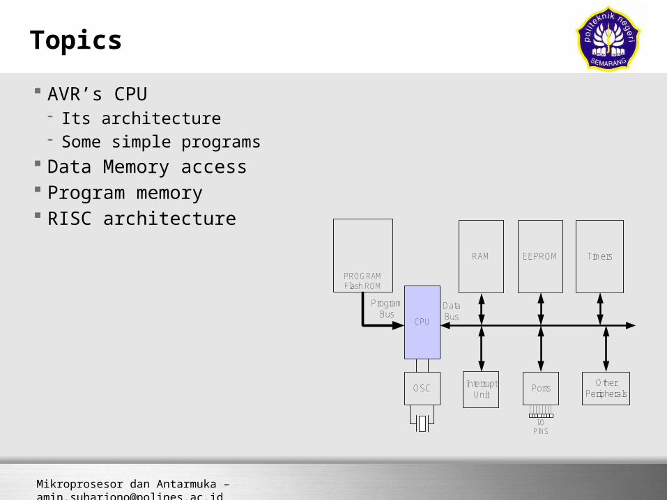
AVR’s CPU- Its architecture - Some simple programs
Data Memory access Program memory RISC architecture
PROGRAM Flash ROM
PortsOSC
CPU
Timers
OtherPeripherals
ProgramBus
Data Bus
RAM
I/O PINS
EEPROM
Interrupt Unit

Mikroprosesor dan Antarmuka – [email protected]
AVR’s CPU
AVR’s CPU- ALU- 32 General Purpose registers
(R0 to R31)- PC register- Instruction decoder- Status Register (SREG)
CPUPC
ALU
registers
R1
R0
R15
R2
…
R16
R17
…
R30
R31
Instruction Register
Instruction decoder
SREG: I T H S V N CZ
Mikroprosesor dan Antarmuka – [email protected]
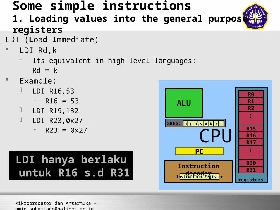
Some simple instructions1. Loading values into the general purpose registers
LDI (Load Immediate) LDI Rd,k
- Its equivalent in high level languages:
Rd = k Example:
- LDI R16,53- R16 = 53
- LDI R19,132- LDI R23,0x27
- R23 = 0x27 CPUPC
ALU
registers
R1R0
R15
R2
…
R16R17
…
R30R31
Instruction Register
Instruction decoder
SREG: I T H S V N CZ
LDI hanya berlaku untuk R16 s.d R31

Mikroprosesor dan Antarmuka – [email protected]
Some simple instructions 2. Arithmetic calculation
There are some instructions for doing Arithmetic and logic operations; such as:
ADD, SUB, MUL, AND, etc. ADD Rd,Rs
- Rd = Rd + Rs- Example:- ADD R25, R9
- R25 = R25 + R9- ADD R17,R30
- R17 = R17 + R30

Mikroprosesor dan Antarmuka – [email protected]
A simple program
Write a program that calculates 19 + 95
LDI R16, 19 ;R16 = 19
LDI R20, 95 ;R20 = 95
ADD R16, R20 ;R16 = R16 + R20
CPUPC
ALU
registers
R1R0
R15
R2
…
R16R17
…
R30R31
Instruction Register
Instruction decoder
SREG: I T H S V N CZ

Mikroprosesor dan Antarmuka – [email protected]
A simple program
Write a program that calculates 19 + 95 + 5
LDI R16, 19 ;R16 = 19
LDI R20, 95 ;R20 = 95
LDI R21, 5 ;R21 = 5
ADD R16, R20 ;R16 = R16 + R20
ADD R16, R21 ;R16 = R16 + R21
LDI R16, 19 ;R16 = 19
LDI R20, 95 ;R20 = 95
ADD R16, R20 ;R16 = R16 + R20
LDI R20, 5 ;R20 = 5
ADD R16, R20 ;R16 = R16 + R20

Mikroprosesor dan Antarmuka – [email protected]
Some simple instructions 2. Arithmetic calculation
SUB Rd,Rs- Rd = Rd - Rs
Example:- SUB R25, R9
- R25 = R25 - R9- SUB R17,R30
- R17 = R17 - R30
CPUPC
ALU
registers
R1R0
R15
R2
…
R16R17
…
R30R31
Instruction Register
Instruction decoder
SREG: I T H S V N CZ

Mikroprosesor dan Antarmuka – [email protected]
R0 thru R15
Only registers in the range R16 to R31 can be loaded immediate. We cannot load a constant into the registers R0 to R15 directly. It would have to be loaded into a valid register first then copied. To load the value of 10 into register zero (R0): Code:
LDI R16,10 ;Set R16 to value of 10 MOV R0,R16 ;Copy contents of R16 to R0

Mikroprosesor dan Antarmuka – [email protected]
Some simple instructions 2. Arithmetic calculation
INC Rd- Rd = Rd + 1
Example:- INC R25
- R25 = R25 + 1
DEC Rd- Rd = Rd - 1
Example:- DEC R23
- R23 = R23 - 1 CPUPC
ALU
registers
R1R0
R15
R2
…
R16R17
…
R30R31
Instruction Register
Instruction decoder
SREG: I T H S V N CZ

Mikroprosesor dan Antarmuka – [email protected]
Data Address Space
PROGRAM ROM
PortsOSC
Timers
OtherPeripherals
ProgramBus
Data Bus
RAM
I/O PINS
EEPROM
Interrupt Unit
General Purpose Registers
CPU
$0000$0001
$0020
General purpose
RAM(SRAM)
R0R1R2
$001F
$005F
R31
...
TWBRTWSR
SPHSREG
...
General Purpose Registers
Standard I/ORegisters
$00$01
$3E$3F
$0060
...
...
Data Address Space
I/O Address
...
8 bit
$FFFF
data busaddress bus
control busDataBus
LDS Rd, addr ;Rd = [addr]
Example:
LDS R1, 0x60
LDS (Load direct from data space)
STS addr,Rd ;[addr]=Rd
Example:
STS 0x60,R15 ; [0x60] = R15
STS (Store direct to data space)Example: Write a program that stores 55 into location 0x80 of RAM.
Solution: LDI R20, 55 ;R20 = 55
STS 0x80, R20 ;[0x80] = R20 = 55
Example: Write a program that copies the contents of location 0x80 of RAM into location 0x81.
Solution: LDS R20, 0x80 ;R20 = [0x80]
STS 0x81, R20 ;[0x81] = R20 = [0x80]
Example: Add contents of location 0x90 to contents of location 0x95 and store the result in location 0x313.
Solution: LDS R20, 0x90 ;R20 = [0x90]
LDS R21, 0x95 ;R21 = [0x95]
ADD R20, R21 ;R20 = R20 + R21
STS 0x313, R20 ;[0x313] = R20
Example: What does the following instruction do?
LDS R20,2
Answer:
It copies the contents of R2 into R20; as 2 is the address of R2.
Example: Store 0x53 into the SPH register. The address of SPH is 0x5E
Solution:
LDI R20, 0x53 ;R20 = 0x53
STS 0x5E, R20 ;SPH = R20


Mikroprosesor dan Antarmuka – [email protected]
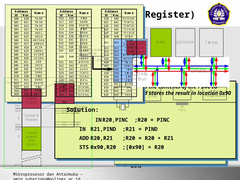
Data Address Space (I/O Register)
PROGRAM ROM
PortsOSC
Timers
OtherPeripherals
ProgramBus
Data Bus
RAM
I/O PINS
EEPROM
Interrupt Unit
General Purpose Registers
CPU
$0000$0001
$0020
General purpose
RAM(SRAM)
R0R1R2
$001F
$005F
R31
...
TWBRTWSR
SPHSREG
...
General Purpose Registers
Standard I/ORegisters
$00$01
$3E$3F
$0060
...
...
Data Address Space
I/O Address
...
8 bit
$FFFF
data busaddress bus
control busDataBus
IN Rd,IOaddress ;Rd = [addr]
Example:
IN R1, 0x3F ;R1 = SREG
IN R17,0x3E ;R17 = SPH
IN (IN from IO location)
OUT IOAddr,Rd ;[addr]=Rd
Example:
OUT 0x3F,R12 ;SREG = R12
OUT 0x3E,R15 ;SPH = R15
OUT (OUT to IO location)
Example:
OUT SPH,R12 ;OUT 0x3E,R12
IN R15,SREG ;IN R15,0x3F
Using Names of IO registers
Example: Write a program that adds the contents of the PINC IO register to the contents of PIND and stores the result in location 0x90 of the SRAM
Solution:
IN R20,PINC ;R20 = PINC
IN R21,PIND ;R21 = PIND
ADD R20,R21 ;R20 = R20 + R21
STS 0x90,R20 ;[0x90] = R20
NameAddressI/O Mem.$00 $20 TWBR$01 $21 TWSR
$04 $24 ADCL$05 $25 ADCH
$02 $22 TWAR$03 $23 TWDR
$06 $26 ADCSRA$07 $27 ADMUX$08 $28 ACSR$09 $29 UBRRL$0A $2A UCSRB$0B $2B UCSRA$0C $2C UDR$0D $2D SPCR$0E $2E SPSR$0F $2F
PIND$10 $30DDRD$11 $31
PORTD$12 $32PINC$13 $33DDRC$14 $34
PORTC$15 $35
PINB$16 $36DDRB$17 $37
PORTB$18 $38PINA$19 $39DDRA$1A $3A
PORTA$1B $3BEECR$1C $3C
EEDR$1D $3D
EEARL$1E $3EEEARH$1F $3F
SPDR
NameAddressI/O Mem.
NameAddressI/O Mem.
UBRRC$20 $40
UBRRH$21 $41 WDTCR$22 $42 ASSR$23 $43 OCR2$24 $44 TCNT2$25 $45 TCCR2$26 $46 ICR1L$27 $47 ICR1H$28 $48 OCR1BL$29 $49 OCR1BH
OCR1AH$2B $4B
SFIOR$30 $50
OCDR$31 $51
OSCCAL$32 $52
TCCR0$33 $53MCUCSR$34 $54MCUCR$35 $55TWCR$36 $56
SPMCR$37 $57TIFR$38 $58
TIMSK$39 $59
TCNT1L$2C $4CTCNT1H$2D $4DTCCR1B$2E $4ETCCR1A$2F $4F
TCNT0
$3A $5AGICR$3B $5BOCR0$3C $5CSPL$3D $5DSPH$3E $5E
GIFR
OCR1AL$2A $4A SREG$3E $5E


Mikroprosesor dan Antarmuka – [email protected]
Status Register (SREG)
CPUPC
ALU
registers
R1R0
R15
R2
…
R16R17
…R30R31
Instruction Register
Instruction decoder
SREG: I T H S V N CZ
$0000$0001
$0020
General purpose
RAM(SRAM)
$001F
$005F
TWBRTWSR
SPHSREG
...
General Purpose Registers
Standard IORegisters
$00$01
$3E$3F
$0060
...
...
Data Address Space
IO Address
...
$FFFF
SREG:
CarryZero
Negative
oVerflow
SignN+VHalf carry
Temporary
Interrupt
H S V N CZTI
Example: Show the status of the C, H, and Z flags after the addition of 0x38 and 0x2F in the following instructions:
LDI R16, 0x38 ;R16 = 0x38
LDI R17, 0x2F ;R17 = 0x2F
ADD R16, R17 ;add R17 to R16
Solution: 1 $38 0011 1000
+ $2F 0010 1111 $67 0110 0111 R16 = 0x67C = 0 because there is no carry beyond the D7 bit.H = 1 because there is a carry from the D3 to the D4 bit.Z = 0 because the R16 (the result) has a value other than 0 after the addition.
Example: Show the status of the C, H, and Z flags after the addition of 0x9C and 0x64 in the following instructions:
LDI R20, 0x9C
LDI R21, 0x64
ADD R20, R21 ;add R21 to R20
Solution: 1 $9C 1001 1100
+ $64 0110 0100 $100 1 0000 0000 R20 = 00C = 1 because there is a carry beyond the D7 bit.H = 1 because there is a carry from the D3 to the D4 bit.Z = 1 because the R20 (the result) has a value 0 in it after the addition.
Example: Show the status of the C, H, and Z flags after the subtraction of 0x23 from 0xA5 in the following instructions:
LDI R20, 0xA5
LDI R21, 0x23
SUB R20, R21 ;subtract R21 from R20
Solution: $A5 1010 0101
- $23 0010 0011$82 1000 0010 R20 = $82
C = 0 because R21 is not bigger than R20 and there is no borrow from D8 bit.Z = 0 because the R20 has a value other than 0 after the subtraction.H = 0 because there is no borrow from D4 to D3.
Example: Show the status of the C, H, and Z flags after the subtraction of 0x73 from 0x52 in the following instructions:
LDI R20, 0x52
LDI R21, 0x73
SUB R20, R21 ;subtract R21 from R20
Solution: $52 0101 0010
- $73 0111 0011$DF 1101 1111 R20 = $DF
C = 1 because R21 is bigger than R20 and there is a borrow from D8 bit.Z = 0 because the R20 has a value other than zero after the subtraction.H = 1 because there is a borrow from D4 to D3.
Example: Show the status of the C, H, and Z flags after the subtraction of 0x9C from 0x9C in the following instructions:
LDI R20, 0x9C
LDI R21, 0x9C
SUB R20, R21 ;subtract R21 from R20
Solution: $9C 1001 1100
- $9C 1001 1100$00 0000 0000 R20 = $00
C = 0 because R21 is not bigger than R20 and there is no borrow from D8 bit.Z = 1 because the R20 is zero after the subtraction.H = 0 because there is no borrow from D4 to D3.