00 cd loth annual solderin9/manufacturing seminar · pdf fileloth annual...
TRANSCRIPT

NWC-TP-. 6707
00
CDloth Annual
Solderin9/manufacturingSeminar Proceedings
Sponsored b•:Electronics manufacturing
Program Office and "T
Soldering Technology Branch DTICtZLECTE•19-20 Februory 1986 MAR 1. 8 1986j 1 5
NAVAL WEAPONS CENTERCHINA LAKE, CA 93555-6001
t N
C-) Approwo d for public relecse: distibution is unlimited.
UJi-_1sAIla C
73est Available Copy
Naval Weapons Center
FOREWORD
The proceedings contained herein are compiled and published by the EngineeringDepartment, Naval Weapons Center, as supporting documentation for the 10th AnnualSoldering/Manufacturing Seminar to be held on 19 and 20 February 1986 at NWC, ChinaLake, CA. This document is a compilation of information--some of it preliminary-that wasprovided by both nongovernment and government sources.
This document, which was prepared for timely prezntation, contains informationdeveloped primarily by sources outside the Naval Weapons Center. The Center assumes noresponsibility for technical or editorial accuracy.
Approved by Under authority ofD. J. RUSSELL, H(ead K. A. DICKERSONEngineering Department Capt., U.S. Navy4 February 1986 Commander
Released for publication byB. W. HAYSTechinical Director
Off-Center request:s for additional copies of these proceedings should beaddressed to the Defense Technical Information Center, Cameron Station,Alexandria, VA 22314-6145. Publications pertinent to the collection of DTICare, with few exceptions, available to authorized requesters.
Copies of specific articles should be requested from the individual authors.
NWC Technical Publication 6707
P iblished by .................................................. Engincering D epartm entCollation ........................................................ Cover, I1 S leavesF irst p rin ting . . . . . . . . . . . . . . . . . . . . . .. . . . . . . . . . . . . . . . . . . . . . . . . . . . . . . . . .. . . . 10 00 co p ies
Best Available CcPs

UNCLASSIFINDISECURITY CLASSIFICATION OF THIS PAGE IWhenBaaIMiat'ere~d) A4 D, A~ //&I: 7f,6.~
REPORT DOCUMENTATION PAGE 9
I.v 114 TIFT 1,11011011 C1AW~IFICA11004 lb HI SFRICTIVIF MAFFKINCA'
UNCLASSIFIED)J1 1,1CUIIUIYPCILAY.,9IAVION AUI111ORIIY 3. 1)g'. F 111W IONIAVAI A FIll FrY Fr RFFPORI
A Statement: Approved for public release: dlistrihution isJb DICI 416`6i ICA IINO'NAFN,~IIntcunli m ited.
4 P*0410RMIN(, ON(.ANNIA11ION ILL PORT1 NUM11 Ott%) S MONI I (FIINI, FFIFANI/A I ION hl POll I NIIMFI R(%)
NWC T11 6707
to.w P4AA I 09 1 RI' F ORVIN4. OIFANF/AF.IION bb OF FiCt llYMFBF) /I. NAM[ OF MONITOFFIN(, OFAtIl/A I iON
Naval Weapons Center ( pI~be
b( ADDRt.(I '.Sho&., '.'~ IP / .)1'(%..) lb 10F A('rSi. j, 1'F.
China Lake, CA 93555-6001
FLA P1MI Of Iql I INVICAPON'ORtINt OINANI/AFIION jKb OF1CId %NMROI qF F'FICUFF(MiNI INSTRIMI, N I 01~ NFFlI CATION NUMVRE R 1
Si ~fr I'((F.SIF.*,iIPF. 10 1.OUFFCF Of F tINPING N IMIFIRIF
FPROGRIAM PROIICI CFS WORl ~IK. UNITrri EMI NT NC NO. NO)N ~
FIt TOIL IF J- m S.'~rwfy 11b w i f.n
Proceedings of the Tenth Annual Solderi ng/M anufactu ring Seminar (U)
F.' PI RONAL AIJIIIFC)RýF)
F1 I. yP OF OttIPORT F lb FFMII COvI RIO) 14 itF OVFF POF T C1ci Poh ~~ FAI: COUN I
Annual From 85 Mar To861iFeh 1986 February 19 19916 .IPFIFIYNFFN
If COW 1F (ODFlI IS 119 IliFICl t I',',~,. I.~C R%' .'z .ild ,'I 1r , 5 ,.,4 nu~mb-),
fillF) VR19 IFFIFF Automated inspection Electronics manUfaturtllingC9 omponent leads Machine vision detection of defect-, rL
130/0 efect analysis (See back of form)7,9 AFI'RA(F IF, ...... 1.1d 1. "n 'AI.'
(U) Presented are the proceedings of the 10th Annual Soldointiig/Ma,,nu~faIcturing Semlinar, held onl 19 and 20Februarv 1986 at the Naval 11veapons Center, China L ake, CA. The proceedings include thle papers or abstrFactsof papers presented at thle Seminar and cover all aspects ol soldering technology and electronics manu~l1faIcturIing.The proceedings are at compilation or informiation-somle of* it prel Il minarv-provided In' bothi nongovernment andgovern mlerit 5911 revs. 14''l( proceed ilgs are Publ ished ill the in itervCst of full hlen ng" comnmun ication and hroo~deniil,awa reniess of' ctirrent activi ties atniiong soilderinog technology and electronics nra nti l'acturi ng spec inlists.
Q UNCLASSIFIED/UNLIMITED N~SAME AS RPT. OJDTIC USERS Lc~isfc
In kroICI ( ; 'f'ck ((;19) Cm939-3.1: oi'10
9 1 APNpFI o e(IIm My lie uwrld U~nti l,9!lFU',F SF CU9~I t' CLASSIII 1A,*T'L) OP T' w, 04(.FEDD FORM 1473, RNI ViAP AFFl~l w FiFV #,&1r, F'p' VF' NC ('As V1SS PII*; )
3est Available COPYmaim**'.

UNCLASSI"I'IF)
SECURl1 Y CLASSIFICATION OF THIS PAGE (Wheln Ihjt Enterldl
18, (Contd.)
Magnification aid/devicesPrinted wiring boardSolder connection inspectionSolder creamsSoldering technology
Soldering technology training programSolder joint failureSolder propertiesStatistical process controlSurface mounted devicesWave solderingWetting balance
'Ik
:':• l.JU NU'IASSI F11) I'
S,.I,.R SE- rI rY CLASS I I:IA T 1IN)lJ D) I l', PACJE t\W lu t Data 1-:titcrmd2' '6
NWC TP 6707 .-
CONTENTS
Introduction .................................................................... 3
Artificial Aging and Component Solderability ........................................ 5David L. Yenawine, Alan Burkett, David Spitz,W. Michael Wolverton, William R. Russell
* Texas InstrumentsDallas, Tex,
Enhancement of Component Lead Protective Finishes for Wave Soldering ............... 45Mark ShiremanHoneywell Inc.Hopkins, Minn, hX: .,
Wetting Balance Solderablity Testing of ElectronicComponents at Receiving Inspection ........................................ 59
J, Gordon DavyWestinghouse Electric Corp.Columbia, Md,
Component Lead Solderability Versus Artificial Steam-Aging .......................... 61R. N, WildIBM Corp,Owego, NY 13827
Q uality Through Training ....................... ................................ 63Joseph SylvesterOmni Training Corp,Covina, Calif.
Proposed Standard for "Magnifying Power" of VisualMagnification Aid/Devices and "Hughes Magnascope" VCalibration Instrument Description and Use ...................................... 71
Donald J. StrittmatterHughes Aircraft CompanyTucson, Ariz, ..
Surface Mounted Devices- Factors Affecting theAdhesive Properties of Synthetic and Rosin-BasedSolder C ream s ................................................................ 93
Norman MacLeod and Larry Hoover .,
Federated-Fry Metals, Inc. PAAltoona, Pa. f."
Automated Inspection of Suirface Mounted Solder" "'Connections-A Status Report on a First Installation .......................... .. 97
Mike Juha ". .. ...IRT Corp. Dlt lbutlo "San Diego. Calif. r
I ("7', Avalllitn Ci e,
"all`%and* .~..* ~* \,Dist

NWC TP 6707
Surface Mounted Technology--Issues and Answers .................................. 109Edmund J. WestcottAir Force Systems CommandAndrews Air Force Base, Md.
Solderability of Capacitor Lead W ires ............................................. 111Alan L. GeigerUnion Carbide Corp.Greenville, SC
Solderability Defect Analysis--Simplified ...................................... 131John A. DeVoreGeneral Electric Co.Syracuse, NY
Solder Defect Mode Analysis Under the "Zero" Defect Concept ........................ 143Frank ZadoAT&T TechnologiesPrinceton, NJ
Dynamic Mechanical Testing of Solder and Solder Joints .......................... 145 I,.Linda D. LauerMartin Marietta Orlando AerospaceOrlando, Fla.
Statistics, Designed Experiments, and Printed Wiring Board Assembly .................. 167Larry R. Lichtenberg, Meridith Sleiman,Mikel J. HarryMotorola Inc.Scottsdale, Ariz.
SReal Time Automated Inspection of SMD Solder Joints ................. ....... 183Todd LaMarcheNicolet Instrument Corp,Madison, Wise.
Circuit Card Assembly Inspection of Surface Mount ComponentsUtilizing a M achine Vision Controller ................................ .......... 187
M. G. (Mike) Buffa .9..
Machine Vision InternationalAnn Arbor, Mich,
* Navy Soldering Technology Training Program .................................. 197William E, SakeNaval Weapons CenterChina Lake, Calif. 1%V
,,,-,, 2
• t '. ,IS.'.
'4 5

NWC TP 6707
INTRODUCTION
The ever-changing, fast-paced technological advances being made today in soldering andelectronics manufacturing present a challenge to us all. To help meet this challenge, we mustwork together. This Seminar-the 10th Annual Soldering/Manufacturing Seminar-gives us anexcellent opportunity to do just that. This Seminar promotes an open exchange of informationon all issues of soldering technology and electronics manufacturing. It provides a forum for allpersons involved in this technology, whether from government, industry, or academia. Here wecan openly discuss these issues and share our ideas. Here we can work together toward ourcommon goal: to improve the U.S. electronics industrial base.
To help make this improvement we must work toward the goals of producibility andquality. We must maintain a concerted effort to resolve production-line problems. First, wemust work to understand these problems. Then, we must develop process controls and methodsto solve them. Because producibility and quality are inseparable, it is critical that our designerslearn from past problems and that they design for ease of manufacturing. The Navy, throughefforts at the Naval Weapons Center, is continuing to work with industry in the SolderingTechnology Branch and in the Electronics Manufacturing Program Office.
The Soldering Technology Branch is continually working to ensure that we meet the goalsof producibility and quality. We evaluate soldering requirements and provide these evaluationsto government and industry facilities. The Navy's work to consolidate its solderingrequirements has resulted in WS-6536E. We are continuing to work with DOD-STD-2000 andexpect a Navy transition to that specification by mid-1987.
Another approach we are taking to improve our electronics industrial base is coordinatedby the Electronics Manufacturing Productivity Facility (EMPF). The EMPF was established atthe Naval Weapons Center in 1984. We are chartered, through the Office of Naval AcquisitionSupport (ONAS), to lead a cooperative effort between electronic equipment manufacturers,product manufacturers, and government agencies to test, evaluate, and research electronicsmanufacturing processes and materials. The EMPF coordinates the cooperative work of thesegroups to develop high-quality processes and to demonstrate high-quality manufacturingdisciplines in a production environment. The EMPF documents this cooperative work anddevelops an accessible information source for electronics manufacturing productivity. Our goalis to gain information, share information, and use information to help produce high qualityproducts at lower cost in less time.
We are indeed looking forward to working with you to improve our electronics industrialbase.
Thank you for your interest in soldering technology and electronics manufacturing and forjoining us at this Seminar.
Chris Peterson Harold PeacockHead HeadSoldering Technology Branch Electronics ManufacturingCode 3681 Program Office
Code 3608

NWC TP 6707
ARTIFICIAL AGINGAND
COMPONENT SOLDERABILITY
BY
DAVID L. YENAWINE, Ph.D.ALAN BURKETTDAVID SPITZ
W. MICHAEL WOLVERTONWILLIAM R. RUSSELL
TEXAS INSTRUMENTSDEFENSE SYSTEMS AND ELECTRONICS GROUP
DALLAS, TEXAS
NLm

NWC TP 6707
INTRODUCT ION----
The NWC Conference has long been one of the most powerful forumson s•oldering and solderability in the country. Participants have .''~
concettrated heavily on the solderability of component leads, andhave had a great effect on how solderability is perceived andmeasured. As a result, numerous specifications have been tightened
to ensure good sollderability. o-.i n t
Our efforts have resulted in an overall industr.y awareness ofsolderability issues that is higher than ever before. But in order
.:" ~to help make further gains in lead solderability we will need to do•':.
more than just demand ever tighter specifications. To date, ourIview of soldering and solderability has been restricted to the:'':component lead, with a goal of making the lead itself more solder- !•
"able. We will need to take a broader view. For the lead is a systemof materials that is part of a larger system of materials making up
Q the component itself. The component is, in turn, part of a largergroup of components that comprise the end-product.
As such, the lead will be subjected to two completely different,manufacturing cycles: assembly into the component, followed by aperiod of storage, and then assembly into the end-product. Allmanufacturing steps, up to the final flow soldering into the printedwiring assembly (PWA), will have an effect on the solderability ofthe lead. Two good examples are axially leaded components and inte-grated circuits.
Axially leaded components can have leads that contain radicallydifferent plating systems. Tin, tin-lead, or gold can be plated overnickel, copper, or Kovar. Some may contain underplating or a barrierplate while others do not. After storage for an undetermined periodof time, the lead is cut, formed, and assembled onto a component .body. A housing or coating, such as epoxy, may be applied, followed"by a curing bake. The finished part may then be subjected to astabilizing bake, or one or more burn-in cycles. After another"undetermined storage period, it is shipped to the end-user.
Integrated circuits follow a similar manufacturing path. Thelead material typically consists of tin or tin-lead over Kovar orAlloy 42. Again after manufacture, the lead frame material is storedfor an unknown period of time. When assembled into a part, it isbonded to a layer of ceramic. once the silicon chip is installed,the lead frame is coated with glass frit and another layer of ceramicand fired. Any oxides resulting from the furnace bake are removedwith an acid bath. Finally, the last two steps involve reflow of theelectroplate or hot solder dip, and the burn-in cycle. The reflowstep may be before or after burn-in. This is then followed bystorage in the manufacturer's warehouse.
• .',4>11
%-N
NWC TP 6707
All of these parts are then shipped to the end-user where theyare stored. Since many companies have a first in, random outwarehouse, the parts could be stored for months or years before beingused in production. After assembly, the PWA may be baked for 6 to 24hours at 105 C to help remove moisture from the printed wiring board,preventing delamination during flow soldering. Finally, the PWA ispreheated and flow soldered.
From this description it is obvious that any effective incomingsolderability screen by the end-user on purchased parts must not onlygauge the state of the plating system following part manufactur-1, butmust also predict the effects of storage and assembly into the PWA.The test contained in MIL-STD-202F, Method 208E is intended to pro-vide the needed solderability screen. A steam aging step for onehour is included in this test to simulate accelerated aging.Recently, questions concerning the validity of the one hour agingstep have arisen. Proposals have been made to increase the time to 8or even 24 hours. (Ref. 1, 2, 3)
This conference has worked hard and has generated a powerful
force to make solderability testing what it wants it to be. We mightbe preparing to be too demanding. We cannot demand what is unattain-able, but must first determine what is needed. When the changes dooccur, both component manufacturers and users must be prepared inadvance. Otherwise, the price will be extensive yield losses andrework.
In order to evaluate the effects of varying amounts of steamaging on part solderability, a representative cross-section of manydifferent types of components contained in the warehouse at TI werechosen. The samples were then subjected to 1, 8, and 16 hours ofsteam aging, and the solderability test performed. The results ofthis testing are presented in Section I of this paper.
As a separate effort, Section II takes a more theoretical lookat the activation energy for intermetallic growth and oxidation of k""the Sn-Pb/Cu system. This section correlates storage time and steamagi ng.
Finally, Section III gives a brief description of TI's effortsto Improve the solderability of stranded wire purchased by thecompany.
7
2..

I
NWC TP 6707
I. AGING STUDY RESULTS
A study was undertaken to determine how the results ofMIL-STD-202F, Method 208E solderability testing would be impacted bysteam aging times of 1, 8, and 16 hours. The samples for the studyform a representative cross-section of the most common componentsused in TI systems and available in the warehouse. The sample matrixencompasses a variety of device types, plating systems, and manufact-urers. In total, 85 lots were included in the study. The method ofpackaging during warehouse storage was not considered. Five samplesper lot were tested at each of the three aging intervals.
Samples from each of the 85 lots were microsectioned in theas-received condition to determine the base metal and the platingsystem, as well as the platinq thickness. Solderability testing was
accomplished using a steam ager built to the MIL-STD-202F, Method208E guidelines, an Electrovert Model WDC flowing solder pot, and anHMP Model 1900 mechanical dipper. Both passing and failing partswere microsectioned following the test. The complete solderabilitytest results are included in the Appendix to this report.
The following tables will summarize the test results. Sixgeneral plating schemes, twelve device types, five date codes, andtwenty- four manufacturers were encompassed in this study. Table Isummarizes the various plating schemes tested, and Table II summar-izes the various device types tested.
Table I: Plating Systems
# Lots
Tin or Tin-Lead over Nickel, Kovar, or Alloy 42 11Gold over Nickel, Kovar, or Alloy 42 3Tin or Tin-Lead over Kovar or Alloy 42 (All DIP ICs) 32Tin or Tin-Lead over Copper over Nickel over Kovar or Alloy 42 3Tin or Tin-Lead over Copper or Copper-Clad-Steel (CCS) 27Gold over Nickel over CCS, Kovar or Alloy 42 9
Table II: Device Types
#I Lots # Lots
Tantalum Capacitor 4 DIP IC 32Polycarbonate Capacitor 3 IC (TO-39, TO-99) 9Ceramic Capacitor 2 IC (TO-3) 3Mica Capacitor 2 Transistor (TO-5) 2Resistor 15 Transistor 2Variable Resistor 3 Diode 8
., .4. .
* ,..";.":-

NWC TP 6707lo
Table III summarizes the overall solderability test results. Ona part basis, only 67% passed the existing MIL-STD-202F, Method 208Esolderability test. On a lot basis, that number falls to 48%. Thenumber of lots that could actually be used would be improved by tin-ning the components utilizing fluxes more active than those used intesting. However, routine tinning is not an attractive dlternative.
The test results appear to be date code independent since bothsample quantities and test failures were equally distributed betweenparts with 1984 and 1985 date codes. This was expected since leadsand lead frames are not assigned a date code and may be stored indef-initely before assembly into a component. Hence the date code as apurchasing parameter relating to solderability may never be of valuebecause of the lack of correlation between component date codes andthe date of lead manufacture. It must be re-emphasized, most ofthese parts have been in storage for 6 months to 1 1./2 years, andsome even longer.
V, .
Table III: Solderability Results By Lead Types
# of Percent PercentLead Type Lots Tested Parts Passing Lots Passin"
1 Hr 8 Hr 16 Hr I Hr 8 Hr 16 Hr
Sn or Sn/Pb over 32 55 23 18 41 13 3Kovar or Alloy 42
Sn or Sn/Pb over Cu 27 81 56 40 56 29 15or Cu-Clad-Steel
Au over Ni over 9 96 91 73 78 66 45Cu-Clad-Steel,Kovar or Alloy 42
Sn or Sn/Pb over Ni, 11 45 27 33 36 18 18Kovar, or Alloy 42
Sn or Sn/Pb over Cu 3 60 13 0 33 0 0
over Ni over Kovaror Alloy 42
Au over Ni, Kovar, 3 60 27 7 33 0 0or Alloy 42
Overall Average 85 67 41 32 48 24 13
9
V,
VS """ :" '- "%,'..--' •'j..•'•w' ,'• '- '°." w''." • '. •'w" .. '.,.•'-.''.," . -. ' ", .. •. •'' ." .' -. °' " ." •' ." •" ;. " ,

NWC TP 6707
Tables IV through IX show detailed test results for each platingsystem. The largest group of samples was DIP ICs, shown in Table IV,having tin or tin-lead coated Kovar or Alloy 42 leads. The resultsshow that 55% passed after one hour of steam aging. The i)ccurrenceof failures appeared to be independent of manufactv , but diddepend greatly on lead treatment. Electroplated and s. ier dippedleads were much more resistant to steam aging than were reflowedleads. Many of the failures were due to edge dewet in varyingdegrees. This can be expected since plating thickness is less neartie edges, especially on reflowed parts.
Parts having leads consisting of tin or tin-lead over copperwhich includes axially leaded capacitors, resistors, and diodesperformed relatively well at one hour. Table V shows that 81% ofthese parts passed. It is worth mentioning that lot numbers 25 and26, of which none passed, were wirewound resistors with stampedleads. Typically, these have performed poorly in our solderabilitytests because the lead forming process uses pre-plated leads. Otherfailures were attributed to thick, brittle Cu-Sn intermetallics andto Cu-Sn intermetallics forming on parts with thin plating; thelatter mechanism consuming all of the free tin. A similar problemarises in platings with high lead contents (70% - 90% wt). Even leads
with 400 microinches of plating become unsolderable because of tindepletion after 100 microinches of intermetallic formation.
Data for the parts having the best overall solderability appearin Table VI, where it is shown that 96% of the parts having gold overnickel passed the Mil-Std solderability test. This is particularlyinteresting when one notes that the gold thicknesses are between 12and 90 microinches. In contrast to this is the data in Table VII.Whereas the ICs in TO- packages performed well with a gold overplate,they performed poorly with a tin or tin-lead overplate. Unfortunate-ly, no determination could be made as to whether this was due to thebase metal preparation or to the overplate itself. !*.
Looking back at Table III it can be seen that 41% of the partspassed after 8 hours of steam aging. As the components are presentlymade, only two plating systems held up reasonably well after extendedaging. Superior was the gold over nickel system where 91% of theparts passed. Next was the tin or tin-lead over copper system with56% of the parts passing. All of the other platings fared badly.The 16 hour aging time results show a further reduction in thepercentage of passing parts to 32%,o, with the gold over nickel andtin or tin-lead over copper plating systems again performing best.
7,1
* 10
N.

NWC. TP 6707
Figures I through 14 show photographs of representative testsamples. They consist of parts which exhibited acceptablesolderability at each steam aging, as well as parts that f.iled ateach steam aging. Cross-sections of each part are also included.Figures 15 and 16 show cross-sections illustrating the variousconditions in which leads have been received at TI. Each ol theseparts had solderability problems either at Incoming or on the assem-bly line. Figure 17 shows a cross-section of a capacitor lead.These parts exhibited dewetting on the assembly line. Attempts weremade to tin the component lead so that they could be used. Figure 18shows another part from the same lot which has been tinned. Note the
Cu3Sn intermetallic compound has been completely removed. The tinnedparts were then solderability tested after extended steam agings. Inno cases did failures occur. This indicates that the effects ofcomponent manufacturing on the leads can be corrected in some cases.
In summary, these test results indicate that the one hour ofsteam aging does not adequately insure shelf lives beyond 6 months.A longer steam aging step should be included to insure not onlyadequate shelf life, but also to insure the parts will be able towithstand the PWA manufacturing cycle. The only reason these partsdo not present a greater problem during assembly is that the solderprocesses have been so finely tuned that compensations have been madefor many of these problems. Ary further increase in the producibility n%of these assemblies must involve an increase in lead solderabilityrather than simply more improvements in soldering techniques.Improvements in lead solderability must account for the effects ofall manufacturing steps, both for the component itself and the PWA.The solderability of the plating system can thereby be optimized, andany deleterious effects compensated for or corrected.
, .-
N
11e
I~t.

NWC TP 6707
TABLE IV: SOLDERABILITY RESULTS -SN OR SN/PB OVER KOVAR OR ALLOY 42 (DIPs)
SN OR SOLDERABILITY TESTINGSN/PB NUMBER PASSED/5 TESTED
ID PART TYPE TREATMENT DC I HR. 8 HR. 16 HR.---------- --------------------------------------- t------------30 DIP IC EP 8437 0 0 031 DIP IC SD 8511 5 3 232 DIP IC R 8448 0 1 034 DIP IC R 8505 2 0 035 DIP IC SD 8438 4 5 436 DIP IC SD 8519 1 0 037 DIP IC EP 8232 1 2 138 DIP IC EP 8311 0 0 039 DIP IC EP 8445 2 3 440 DIP IC R 8423 0 0 041 DIP IC EP 8442 5 3 442 DIP IC SD 8412 2 0 043 DIP IC SD 8516 5 0 044 DIP IC EP 8416 0 0 045 DIP IC R 8442 1 0 046 DIP IC R 8522 0 0 047 DIP IC EP 8436 5 0 248 DIP IC EP 8502 5 5 549 DIP IC EP 8429 5 2 050 DIP IC EP 8303 4 0 051 DIP IC SD 8505 5 0 052 DIP IC EP 8430 3 1 154 DIP IC SD 8520 2 0 055 DIP IC EP 8537 5 5 456 DIP IC R 8503 0 0 059 DIP IC EP ???? 5 2 180 1)I1P IC R 8425 5 0 081 DIP IC R 8504 1 0 082 DIP IC SD 8427 5 0 083 DIP IC SD 8534 5 5 084 DIP IC EP 8509 5 0 185 DIP IC R 8431 0 0 0
OVERALL TOTAL 88 37 29% PASSING 55 23 10
ELECTROPLATED (EP) TOTAL 45 23 23% PASSING 64 32 32
REFLOWED ELECTROPLATE (R) TOTAL 9 0 0% PASSING 20 0 0
HOT SOLDER DIPPED (SD) TOTAL 34 13 6% PASSING 76 32 15
12
, . ,.,.,
~ p p i - p ..•

,4<
NWC TP 6707
TABLE V: SOLOERABILITY RESULTS -SN OR SN/PB OVER CU OR CU-CLAD-STEEL
SOLDERABILITY TESTINGNUMBER PASSED/5 TESTED
ID PART TYPE DC I HR. 8 HR. 16 HR.3- -- CB------- CAPACITOR-------4-2-
3 POLYCARB CAPACITOR 8438 4 2 2A. POLYCARB CAPACITOR 8434 5 4 5
5 POLYCARB CAPACITOR 8438 3 2 18 CERAMIC CAPACITOR 8545 5 3 09 CERAMIC CAPACITOR 8518 4 0 114 MICA CAPACITOR 8523 5 3 015 MICA CAPACITOR 8542 5 2 56 RESISTOR 8449 5 4 27 RESISTOR 8505 5 4 410 RESISTOR 8530 5 5 011 RESISTOR 8325 5 5 512 RESISTOR 8401 5 3 013 RESISTOR 8343 3 3 018 RESISTOR ???? 0 0 119 RESISTOR 8414 4 5 223 RESISTOR 8503 5 0 524 RESISTOR 8443 5 2 325 RESISTOR 8446 0 0 026 RESISTOR 8327 0 0 028 RESISTOR 8416 5 0 229 RESISTOR 8439 4 0 0 .,:
69 DIODE 8520 5 4 470 DIODE 8444 5 5 472 DIODE 8516 5 5 3
73 DIODE ??? 4 5 074 DIODE 8525 4 5 475 DIODE 8407 4 5 1
"TOTAL 109 76 54% PASSING 81 56 40
13 .. 13
An -,

NWC TP 6707
TABLE VI: SOLDERABILITY RESULTS -
AU OVER NI OVER CCS, KOVAR, OR ALLOY 42
SOLDERABILITY TESTINGNUMBER PASSED/5 TESTED
ID PART TYPE DC I HR. 8 HR. 16 HR.
58 IC (TO-99) 8424 5 4 460 IC ýTO-391 8525 5 5 561 IC TO-99 8342 5 5 563 IC (TO-99) 8530 5 3 265 IC TO-39 8435 4 5 367 IC TO-99) 8510 5 5 571 TRANSISTOR 8428 5 4 176 DIODE 8441 5 5 577 DIODE 8525 4 5 3
TOTAL 43 41 33% PASSING 96 91 73
TABLE VII: SOLDERABILITY RESULTS -
SN OR SN/PB OVER NI, KOVAR, OR ALLOY 42
SOLDERABILITY TESTINGNUMBER PASSED/5 TESTED
ID PART TYPE DC 1 HR. 8 HR. 16 HR. a1 TANTALUM CAPACITOR 8320 5 5 42 TANTALUM CAPACITOR 8250 4 2 2
16 TANTALUM CAPACITOR 8516 5 1 517 TANTALUM CAPACITOR 8541 5 2 222 RESISTOR 8348 5 5 527 VAR. RESISTOR 8109 0 0 033 IC (10-3) 8216 0 0 057 IC (TO-99) 8009 0 0 062 IC (TO-3) 8505 0 0 066 IC (TO-99) 8315 1 0 068 TRANSISTOR 8509 0 0 0
TOTAL 25 15 18% PASSING 45 27 33
14

NWC TP 6707
TABLE VIII: SOLDERABILITY RESULTS -
SN OR SN/PB OVER CU OVER NI OVER KOVAROR ALLOY 42
SOLDERABILITY TESTINGNUMBER PASSED/5 TESTED
ID PART TYPE DC 1 HR. 8 HR. 16 HR.-- --------- - -----------53 IC (TO-3) 8526 3 0 0
78 TRANSISTOR (TO-5) 8505 5 2 079 TRANSISTOR (TO-5) 8445 1 0 0
TOTAL 9 2 0% PASSING 60 13 0
A6
TABLE IX: SOLDERABILITY RESULTS -AU OVER NI, KOVAR, OR ALLOY 42
SOLDERABILITY TESTINGNUMBER PASSED/5 TESTEDID PART TYPE DC 1 HR. 8 HR. 16 HR.-........ -- -- -
20 VAR. RESISTOR 8528 5 2 121 VAR. RESISTOR 8445 3 1 064 IC (TO-39) 8440 1 1 o0I, TOTAL 9 4 1
% PASSING 60 27 7
b *1o
15 , -
io' pW' L

NWC TP 6707
A 7"
1 16

3 "V.
NWC TP 6707
Fiue I andt2
." I2 'Y
14,
FIGURE 3 Crs-eto Rfth esistor lead exiitn poor sodrbltsoigdwtigafter 8 hour steam aging.,hspr a rmK
17~

NWC TP 6707
FIGURE 5 IC lead consisting of tin-lead over KovarK:; that exhibited good solderability afteroehour steam aging.
0.
FIGURE 6 -Cross-section of IC lead in Fig. 5 showingcondition of solder coat over Kovar basemlletalI. (500X)
18
1%X

NWC TP 6707
IiFIGURE 7 -IC lead consisting of tin-lead over Kovarexhibiting poor solderability after 8 hoursteam aging. This part was from same samplelot as the lead shown in figure 5.
FIGURE 8 C ross-section of IC lead shown in Fig. 7,
showing areas of dewet. (500X)
19

NWC TP 6707 1
71'
17 %
FIGURE 9 -A variable resistor lead consisting of goldover nickel, exhibiting poor solderabilityafter 8 hours.
4..
FIGURE 10 -IC leads consisting of solder over Kovar,exhibiting poor solderability after 8 hour
*steaM aging.
20
NWC TP 6707
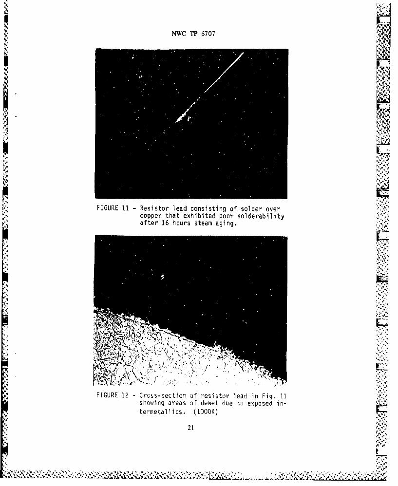
FIGURE 11 -Resistor lead consisting of solder overcopper that exhibited poor solderability .
after 16 hours steam aging.
temtlis (100 .)
'121

NWC Ti' 6707
qIUE1 Cla ossigo odroe oa
test.
21.'

NWC TP 6707
FIGURE 15 - These two photographs show opposite sidesof one cross-section on a copper clad steelcapacitor 'lead having a tin-lead coating.The capacitor manufacturing processes causeda thick build-up of intermetallics. Anattempt at rework was made, but the hotsolder dip did not completely dissolve theCu3Sn layer on one side of the lead. Thiscaused a subsequent dewet problem during'flow soldering. (1000X)
I.TI
23
eli

'1 NWC TP 6707
0,,
FIGURE 16 -Two photographs showing the varying con-ditions in which leads have been receivedon incoming parts. (1000X)
-w I
14H
24
=7--

QNWC TP 6707
I%
FIGURE 17 - Cross-section of a capacitor lead inas-received condition, showing thickintermetallic layer resulting from thecapacitor manufacturing processes. (iQOX)
V.4
FIGURE 18 - A cross-section of the other lead from thesame capacitor, after hot~-tin dip, showingthat the intermetallic layers were removed. '•
25,,; - A4
,•,,'..• " -' , , • 4 • • • " .'.,.-'•...,.., .,,. .. ,"... i,•,?,?':.•-'.'-•','r- V A',"-".':%, i ii i i i ' i ' i0A
NWC TP 6707
II. CORRELATION OF ACCELERATED AGING TESTS AND ROOM TEMPERATURE STORAGE
Component users want an incoming test that adequately screensout marginal components without being overly demanding of componentsuppliers. Therefore, experiments and calculations were carried outthat directly correlate accelerated aging times with room temperaturestorage times. Also determined were the aging mechanisms that occurin different aging environments. This first study focused on thetin-lead-on-copper system.
The two subsystems analyzed were 1) dry aging (i.e. oven baking)of 60/40 tin-lead plated copper leads and 2) 90-100% relative
humidity aging and dry aging of copper leads coated with 63/37tin-lead by the dipping procedure as described in MIL-STD-202F,Method 208E. It was suspected that the primary aging mechanism in thefirst subsystem would be solder consumption by copper-tinintermetallic compound (IMC) formation. The aging mechanism of thesecond subsystem was suspected to also include solder consumption byoxidation of the solder surface exposed to moisture in air as shownin Figure 18A. Therefore, we characterized the aged specimens withphotomicrographs to show IMC thicknesses, and with Auger spectroscopyto measure oxide thicknesses below the solder surface. Five samplesper test group were also redipped using an R flux and visuallyinspected at IOX to 20X magnification for solderability, using the
pass/fail criteria of MIL-STD-202F.
The electroplated copper leads were 22 gauge copper wire with440 microinches of plated solder. The solder was not fused. Figure19 shows how Cu3Sn and Cu6Sn5 intermetallics grew over time at 150 C. •
This figure implies IMC formation by Fickian diffusion, since thecurves are approximately parabolic, and from Fick's Law,
(1) D = L 2 / t,
where D is the diffusivity (i.e. diffusion constant), L is the diffu-sion length (i.e. the solder thickness consumed in aging), and t isdiffusion time. For a given aging environment, D is constant, and
(2) t c L.
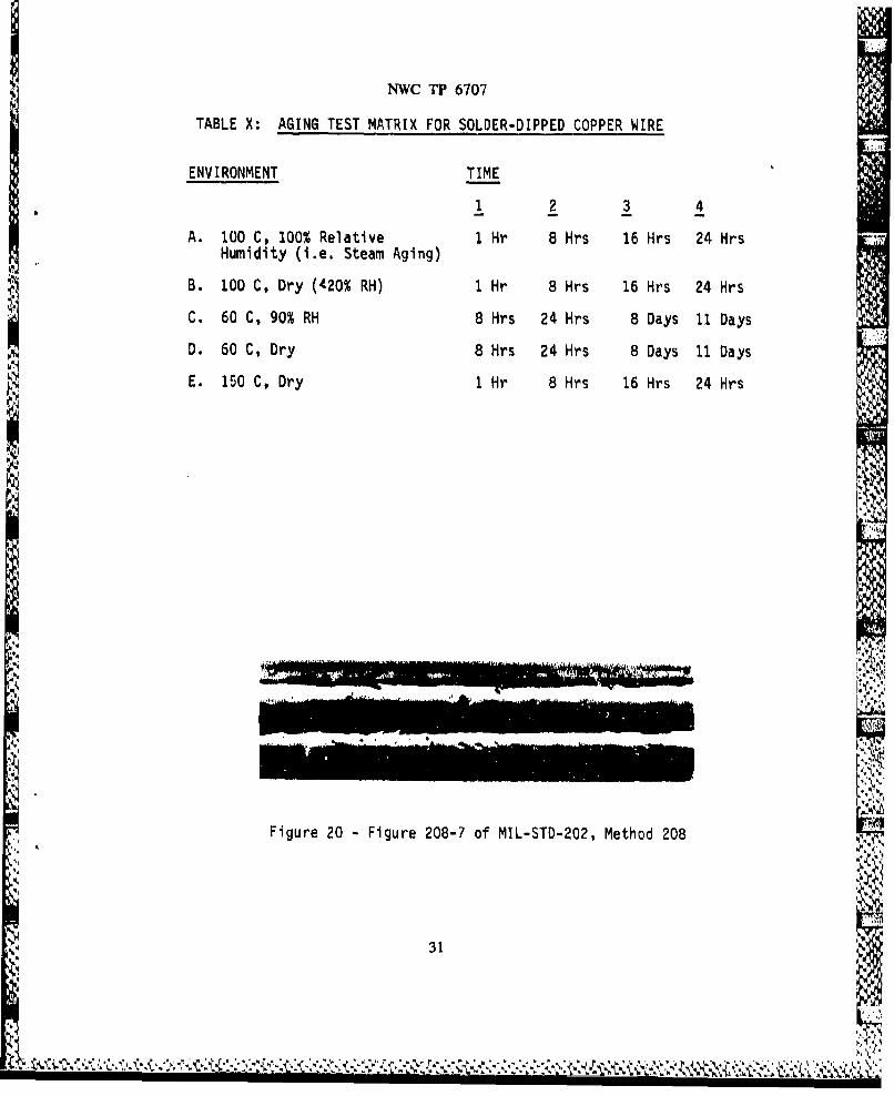
The solder-dipped copper leads were 20 gauge copper wire with
300 to 400 microinches of original solder thickness. The sampleswere aged per the test matrix of Table X. IMC data was measured intwelve places per test group. It was found that the control samples(i.e. unaged) and test groups A4 (i.e. 24 hours steam aging) and E4(i.e. 24 hours at 150 C oven baking) all had average IMC thicknessesof 70 to 75 microinches. The IMC in these groups was Cu6Sn5, None
26

NWC TP 6707
was Cu3Sn. It was concluded that solder-dipped copper has superiormetallurgical stability to solder-plated copper. A brief explanationfollows.
It is well known that Cu6Sn5 forms between the copper and thesolder during soldering, probably by an electrochemical reaction(Ref. 4), where the flux reacts with tin to form tin chloride in theflux, then tin from the tin chloride deposits onto the copper as anintermetallic (Ref. 5). Lead and copper do not form an IMG, so onlythe tin-copper IMC is formed. When Cu3Sn forms next to the Cu6 Sn5,the large lattice mismatch between these two brittle IMCs increasesthe likelihood of breakage on a microscopic scale. Twenty-four hoursof 150 C aging causes Cu3Sn to form in the electroplated material,but. not in the dipped material since the dipped material has arelatively diffusion-resistant microstructure.
There are two reasons for the relative metallurgical stabilityof dipped material. First, the concentration gradient (i.e. coppernext to Cu6Sns next to solder) is less, and thus the driving forcefor diffusion is less than in plated material (i.e. copper next tosolder). Secondly, less porous, larger and more tightly packedcrystals occur with solder dipping than with unfused solder plating(Ref. 6).
The test groups of Table X were solderability tested per thepass/fail standard of Figure 20. The results are shown in Table XI.Only the high humidity environments produced solderability failures.The failures occurred at 8 hours with 100 C aging, but not until 8days with 60 C aging.
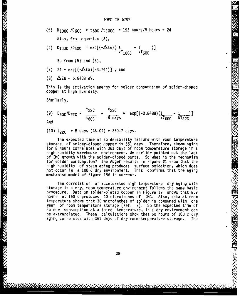
With data at these two temperatures, an extrapolation can bemade to obtain the expected time of solderability failure at a thirdtemperature, namely, room temperature (e.g. 22 C). This is possible,since the temperature-dependence of the diffusion constant, 0,generally follows an Arhennius-type relationship:
(3) D = D..exp (-&Ea/kT)
where D.. is a constant, AEa is the activation energy, k isBoltzmann's constant, and T is the absolute temperature of aging, indegrees Kelvin.
Solderability is lost when solder thickness, L, is consumed atany temperature. So from equation (1),
(4) Do1 I/t ,and
27.I r I r
9q.
NWC TP 6707
(5) DIOOC /D60C = t60C /tlOOC = 192 hours/8 hours = 24
Also, from equation (3),
(6) DIOOC /D60C = exp[(-AEa)( 1 - 1
'RTTO0C I"'60C
So from (5) and (6),
(7) 24 = exp[(-AEa)(-3.744)] , and
(8) AEa = 0.8488 eV.
This is the activation energy for solder consumption of solder-dippedcopper at high humidity.
Similarly,
t22c t2
(9) D60C/D22C = t 22C____ exp[(-0.8488)(1_ - 1 )1
And T60C 8a0C
(10) t 2 2C = 8 days (45.09) = 360.7 days.
The expected time of solderability failure with room temperaturestorage of solder-dipped copper is 361 days. Therefore, steam agingfor 8 hours correlates with 361 days of room temperature storage in ahigh humidity warehouse environment. We earlier pointed out the lackof IMC growth with the solder-dipped parts. So what is the mechanismfor solder consumption? The Auger results in Figure 21 show that thehigh humidity of steam aging produces surface oxidation, which doesnot occur in a 100 C dry environment. This confirms that the agingmechanism model of Figure 18A is correct.
The correlation of accelerated high temperature dry aging withstorage in a dry, room-temperature environment follows the same basic
procedure. Data on solder-plated copper in Figure 19 shows that 8.9hours at 150 C produces 40 microinches of IMC. Also, data at roomtemperature shows that 30 microinches of solder is consumed with oneyear of room temperature storage (Ref. 7). So the expected time ofsolder consumption at a third temperature, in a dry environment canbe extrapolated. These calculations show that 50 hours of 100 C dryaging correlates with 361 days of dry room-temperature storage. The
"A'
280,A
4,,IW

NWC TP 6707
AS DIPPED
Cu6 Sn 5 Intermetallic
Compound (IMC)
COPPER TIN-LEAD AIR
I ,W4- X-b__4
AGED
I 0COPPER M TIN- X AIR
C LEAD IDE
x-Ax
A X is the amount of solder thickness that isconsumed by solid-state-diffusion growth of inter-metallic and by oxidation.
t%•
FIGURE 18A: AGING MECHANISM MODEL
29

NWC Tl' 6707
Sleo TIN PLATING€.• 150S14,0
130S120
• eo
•- mO.•o / Cu3Sn ,/ -ooSBO • o
3O
• •o
o 2'4 4', 7'• ;, ,•o •44 I•----
TIME, HOURS
•'•L•
•.• 160-,- Iso TIN/LEAD PLATINGz 14o.,130
120
1101 O0
•: 9o
• 7oF- 80• so• 4o
• •o
o 0 2',• 4.8
TIME, HOURS
FIGURE 19: INTERMETALLIC GROWTH AT 150°C
w• •.•• , 30 """"4
'I 'J" °%""I•" ImZ
.,•
i•',k".'•'•,,'•,•",•i•'•,'2•,,.'r,;\%\•,'•'.,•2• ?•V•?,•.•',".v;•,'.•.•.','.V',,• ,., \ ', : ,.,, ,,' ,' 2. - ','.'.•," "e; ,' ".•','.','o','.' ",'; "•," .';.'2,';,.',.'g.'.'••. ,',.'•'....'. '•',.,' &'i. '•',.••'•'•.•.,
NWC TP 6707
TABLE X: AGING TEST MATRIX FOR SOLDER-DIPPED COPPER WIRE
ENVIRONMENT TIME
1 2 3.A. 100 C, 100% Relative 1 Hr 8 Hrs 16 Hrs 24 Hrs
Humidity (i.e. Steam Aging)
B. 100 C, Dry (420% RH) 1 Hr 8 Hrs 16 Hrs 24 Hrs
C. 60 C, 90% RH 8 Hrs 24 Hrs 8 Days 11 Days
D. 60 C, Dry 8 Hrs 24 Hrs 8 Days 11 Days
E. 150 C, Dry 1lHr 8 Hrs 16 Hrs 24 Hrs
Figure 20 -Figure 208-7 of MIL-STO-202, Method 208
31

NWC TP 6 7U7
TABLE XI: SOLDERABILITY TEST DATA
TEST GROUP(*) SAMPLES PASSED/SAMPLES TESTED
CONTROLS (NOT AGED) 5/5Al 5/5
A2 1/5A3 1/5A4 0/5
BI 5/5B2 5/5B3 5/5B4 5/5
Cl 5/5C2 5/5C3 3/5C4 3/5
D1 5/5D2 5/5D3 5/5D4 5/5
El 5/5E2 5/5E3 5/5E4 5/5
*Looking at Table X, C3 would be 60 C, 90% RH
for 8 days.
32
j -,,', ;
:K, '','.'

NWC TP 6707
OXYGEN ATOMIC PERC•NTAT A DEPTH OF
TEST GROUP 900 ANGSTROMS 1800 ANGSTROMS
CONTROL 0 0
Al 39.2 24.8
A2 25.4 9.0
A4 35.6 35.8
BI 0 0
B2 0 0
B4 0 0
FIGURE 21A: AUGER SPECTROSCOPY OXYGEN DATA SHOWING RELATIVEAMOUNTS OF SOLDER SURFACE OXIDATION
A ~~100. __
70
60
40-
WA 30-
20-
10
0 go0 1UO0 2700 3600
Sputter Dth from Surface sAniatromm)SuARBON + TFN O ENLAD
FIGURE 21B: TYPICAL AUGER DEPTH PROFILE
33
14ý N

NWC TP 6707
2-----
4.-4
2 .2 2.4 ...2.. 32 .4 3.,,
S......
FIUE2: AHNISPLTFRDYAIGO ECTOLAE SOLDER
ON C PPE * .. .. ... -
34x

NWC TP 6707
activation energy here is relatively low, 0.6266 eV, because it takesless energy to activate IMC growth in an electroplated part than in adipped part.
The diffusion constants, expressed in microinches squared perhour, for various temperatures are: 179 at 150 C, 17.9 at 100 C, 1.71at 60 C, and 0.103 at 22 C. An Arhennius plot, zhowing the diffusionconstant as a function of any temperature is shown in Figure 22.
This section has illustrated one method to correlate acceleratedaging tests with room temperature storage. Specific correlationshave been calculated, namely, 8 hours of steam aging corresponds tothe same loss of solderability as about one year of high-humidity,room- temperature storage, for solder-dipped copper leads. Thisinitial finding can be verified by experiments and calculationssimilar to those described in this section, as well as by long-termstorage tests.
III. STRANDED WIRE
In mid-1984, TI found itself rejecting 60% of the incoming tinplated, stranded wire because of solderability failures. Anextensive effort was undertaken to correct that situation by workingclosely with the wire manufacturers. As part of the larger TI vendorreduction plan, the number of wire vendors was cut, allowing for moreefficient communication with those vendors able to supply themajority of TI's wire requirements. Many lessons were learned. ,.,"
First, it was found that, like other components, stranded wireis made in several steps by two or three different companies.Second, it became apparent that the Mil-Specs governing stranded wirewere inadequate since they did not require a minimum platingthickness on tin plated wire and often did not require solderability
Ni testing. The final lesson learned applies well to the theme of thispaper. In visiting the vendors' facilities, insight was gained into
* what was or was not possible for them to do. In turn, it was thenpossible to offer suggestions and corrective actions. As a result ofthese efforts, the rejection rate is now only 6% at IncomingInspection.
SUMMARY
Solderability tests on a representative sample of the most com-
mon parts stored in the warehouse indicate that half would not passthe MIL-STD-202F, Method 208E test at this point. This indicates
35
S . .. .. • . mm l I I I i

NWC TP 6707
that the one hour steam aging test currently performed is not anadequate incoming solderability screen to allow storage times up to1 year in the warehouse. Leads having tin or tin-lead over copper, orgold over nickel performed best both at one and eight hour agingtimes. Again, finely tuned soldering processes, the tinning ofcomponents, and the use of more active fluxes prevent us from seeingproblems of this magnitude at the board assembly level.
In order to better explore what aging time would be adequate,another study was made to more closely examine the exact mechanismsthat occur in different aging environments. Dry aging of solder-plated copper produced intermetallic compound growth. High-humidityaging of solder-dipped copper produced solder surface oxidation.Solder consumption rates and activation energies were calculated fromexperimental data. These calculations show that 8 hours of steamaging corresponds to the same loss of solderability as about one yearof high-humidity, room-temperature storage, for solder-dipped copperleads. This conclusion is considered a preliminary, initial findingthat should be reconfirmed with extensive empirical data before it isgenerally applied.
Care must be taken not to prematurely insist on more stringentsolderability specifications. First, a determination must be made ofwhat is needed and what is possible. Improvements in lead solderabi-lity can only be made with a more detailed knowledge of the exactplating systems involved and by determining the exact effect thatall subsequent manufacturing steps will have on these materials; frominitial lead forming through component assembly, storage and assemblyinto the system. The solderability of the lead plating system canthen be optimized by compensating for or eliminating those processesthat cause deleterious effects.
Similar to the familiar situation with leaded components, 1 hourappears to be an insufficient steam aging time for incoming inspec-
tion of surface mounted components. Solderability is presently amajor problem with surface mounted components (Ref. 8). Another key
reliability factor for surface mounted electronic assemblies is the '
coefficient of thermal expansion (CTE), not just the different CTEs"- of the device and the substrate, but also of the solder itself (Ref.
9). The high solder CTE cart be the driving force for metallurgicalinstability of surface mounted assemblies.
Future tests are planned to correlate accelerated aging withroom temperature storage for plating systems other than tin-lead overcopper. Additionally, further aging studies on actual components areplanned, including surface mounted devices. Test plans will considerstorage conditions and the extent to which solderability test resultscorrelate with actual component-to-board solderability.
36
.,:2

NWC TP 6707
CONCLUSIONS
Extensive aging, lead charactorization, and solderability test-ing have shown that certain classes of parts would not solder well.We have studied component leads and how they are handled and havefound a considerable risk that large numbers of components will notpass 8 hour steam aging.
As the 8 hour requirement comes into force, there will be twoeffects. A sudden disruption of the industry may occur and wouldcontinue until the older, poorly solderable components are flushedout of the system. Next will begin the era we have worked toward foryears; the era in which no components will be sold that do riot solderwell as stored and used by industry.
This is the conference at which we should sound the clarion toalert component makers and users to the risk that faces them.Everyone should learn from the example set by the IC industry 4 yearsago when DESC changed Mil-M-38510 and required the reflow of all ICleads. The IC industry chose to ignore the impact of the DESC orderon component solderability. That action on the part of the ICindustry cost substantial amounts of money in terms of yield andrework. If the component makers and users do not prepare in advancefor 8 hours of steam aging, the results will be similar and we willhave no one to blame but ourselves. I
ACKNOWLEDGEMENTS.
The authors wish to thank Ne'la Strobel, Senior Metallographer, andDot Bell, Metallographer, for preparing the cross-sections and photo-micrographs in this paper, and Barbara Waller for her help in editingthe manuscript.
37
NWC TP 6707
REFERENCES
1. D.L. Yenawine et. al., "Component Lead and Wire Solderability,"Proceedings 9th Annual Soldering Technology Seminar, NavalWeapons Center, China Lake, California, February 19-20, 1985.
2. R.N. Wild, "Some Component Lead Soldering Issues Phase II",presented at 9th Annual Soldering Technology Seminar, NavalWeapons Center, China Lake, California, February 19-20, 1985, IBM85A80083.
"3. "Accelerated Aging for Solderability Evaluation", IPC report
IPC-,TR464, 1984.4. G.L.J. Bailey and H.C. Watkins, "The Flow of Liquid Metals on
Solid Metal Surfaces and Its Relation to Soldering, Brazing, andHot-Dip Coating," Journal of the Institute of Metals, Vol. 80,1951-52, p. 64.
5. N.K. Batra et. al., "Flux Reactions in Soldering," WeldingResearch Supplement to The Welding Journal, October, 1974, p.424.
6. Paul Davis, Tin Institute, comment in: "Minutes of the ThirdAnnual Joint Industry-Military Lead Solderability Conference,"Texas Inst-i'uments, 1985.
7. B.M. Cox, "Causes and Remedies for Poor Solderability ofComponent Leads", Proceedings 9th Annual Soldering TechnologySeminar, Naval Weapons Center, China Lake, California, February19-20, 1985, p. 10.
8. Surface Mount Technology, The International Society for HybridMicroelectronics, Silver Spring, Maryland, 1984, p. 269.
9. E.A. Wright and W.M. Wolverton, "The Effect of the Solder ReflowMethod and Joint Design on the Thermal Fatigue Life of LeadlessChip Carrier Solder Joints," Proceedings 34th Electronic Compon-ents Conference, IEEE 84CH2030-5, 1984, pg. 149.
3'.rq

NWC TP 6707APPENDIX
AGING STUDY TEST RESULTSTESTING DATA
SOLDERABILITY TESTINGDATE NUMBER PASSED/5 TESTED
ID PART TYPE MFR CODE 1 HR. 8 HR. 16 HR.-- -----------------------------------------
I TANTALUM CAPACITOR A 8320 5 5 42 TANTALUM CAPACITOR B 8250 4 2 23 POLYCARB CAPACITOR C 8438 4 2 24 POLYCARB CAPACITOR A 8434 5 4 55 POLYCARB CAPACITOR B 8438 3 2 16 RESISTOR D 8449 5 4 27 RESISTOR D 8505 5 4 4"8 CERAMIC CAPACITOR E 8545 5 3 09 CERAMIC CAPACITOR E 8518 4 0 110 RESISTOR F 8530 5 5 011 RESISTOR F 8325 5 5 512 RESISTOR G 8401 5 3 013 RESISTOR 8343 3 3 014 MICA CAPACITOR H 8523 5 3 015 MICA CAPACiTOR I 8542 5 2 516 TANTALUM CAPACITOR B 8516 5 1 517 TANTALUM CAPACITOR 8541 5 2 218 RESISTOR J 0 0 119 RESISTOR Y 8414 4 5 220 VAR. RESISTOR J 8528 5 2 121 VAR. RESISTOR J 8445 3 1 022 RESISTOR K 8348 5 5 523 RESISTOR F 8503 5 0 524 RESISTOR F 8443 5 2 325 RESISTOR F 8446 0 0 026 RESISTOR L 8327 0 0 027 VAR. RESISTOR M 8109? 0 0 0
29 RESISTOR F 8439 4 0 030 DIP IC N 8437 0 0 031 DIP IC 0 8511 5 3 232 DIP IC P 8448 0 1 0 1...33 IC (TO-3) P 8216 0 0 034 DIP IC P 8505 2 0 035 DIP IC 0 8438 4 5 436 DIP IC Q 8519 1 0 037 DIP IC N 8232 1 2 138 DIP IC 0 8311 0 0 039 DIP IC R 8446 2 3 440 DIP IC S 8423 0 0 041 DIP IC T 8442 5 3 442 DIP IC N 8412 2 0 0
39

NWC TP 6707
APPENDIX (CONT)
AGING STUDY TEST RESULTSTESTING DATA
SOLDERABILITY TESTINGDATE NUMBER PASSED/5 TESTED
ID PART TYPE MFR CODE 1 HR. 8 HR. 16 HR.------ --------------------- --- ----------------------
43 DIP IC 0 8516 5 0 044 DIP IC N 8416 0 0 045 DIP IC P 8442 1 0 046 DIP IC S 8522 0 0 047 DIP IC 0 8436 5 0 248 DIP IC 0 8502 5 5 549 DIP IC P 8429 5 2 050 DIP IC S 8303? 4 0 051 DIP IC 0 8505 5 0 052 DIP IC S 8430 3 1 153 IC (TO-3) P 8526 3 0 054 DIP IC N 8520 2 0 055 DIP IC U 8537 5 5 456 DIP IC V 8503 0 0 057 IC (TO-99) S 8009 0 0 058 IC (TO-99) N 8424 5 4 459 DIP IC 0 5 2 160 IC TO-39) N 8525 5 5 561 IC TO-39) N 8342 5 5 562 IC TO-3) N 8505 0 0 063 IC TO-99) W 8530 5 3 264 IC TO-39 P 8440 1 1 065 IC TO-39 P 8435 4 5 366 IC (TO-99) 8315 1 0 067 IC (TO-99) P 8510 5 5 568 TRANSISTOR X 8509 0 0 069 DIODE X 8520 5 4 470 DIODE X 8444 5 5 471 TRANSISTOR S 8428 5 4 172 DIODE 8516 5 5 373 DIODE X 4 5 074 DIODE X 8525 4 5 475 DIODE 84,07 4 5 176 DIODE S 8441 5 5 577 DIODE 5 8525 4 5 378 TRANSISTOR (TO-5) S 8505 5 2 079 TRANSISTOR (TO-S) S 8445 1 0 080 DIP IC P 8425 5 0 081 DIP IC P 8504 1 0 082 DIP IC N 8427 5 0 083 DIP IC W 8534 5 5 084 DIP IC W 8509 5 0 185 DIP IC P 8431 0 0 0
40

ImNWC TP 6707
APPENDIX (CONT)
AGING STUDY TEST RESULTS"PLATING DATA
SN OR SN ORBASE SN/PB SN/PB IM AU NI
ID PART TYPE MFR METAL AVE MIN AVE. AVE. AVE.
1 TANTALUM CAPACITOR A NI,42 284 2312 TANTALUM CAPACITOR B NI,42 332 3003 POLYCARB CAPACITOR C CCS 191 724 POLYCARB CAPACITOR A CCS 393 249 935 POLYCARB CAPACITOR B CCS 433 219 1506 RESISTOR D CU 835 735 597 RESISTOR D CU 769 702 788 CERAMIC CAPACITOR E CU 431 339 1069 CERAMIC CAPACITOR E CU 461 375 3910 RESISTOR F CCS 497 300 4311 RESISTOR F CCS 253 195 3312 RESISTOR G CU 525 315 9813 RESISTOR CU 338 246 13814 MICA CAPACITOR H CCS 407 255 *9815 MICA CAPACITOR I CCS 364 153 1716 TANTALUM CAPACITOR B NI,42 25
17 TANTALUM CAPACITOR NI,42 282 22518 RESISTOR J CU 197 9819 RESISTOR Y CU 247 189 7820 VAR. RESISTOR J NI,42 2821 VAR. RESISTOR J NI,42 2322 RESISTOR K NI,42 454 25523 RESISTOR F CU 401 369 11824 RESISTOR F CU 321 249 2825 RESISTOR F CU 958 69926 RESISTOR L CU 265 159 3727 VAR. RESISTOR M NI,42 200 9628 RESISTOR F CU 342 24629 RESISTOR F CU 493 396 2730 DIP IC N 42 232 20731 DIp IC 0 42 593 52532 DIP IC P 42 243 11833 IC (TO-3) P NI,42 540 30034 DIP IC p 42 181 7135 DIP IC 0 42 330 24736 DIP IC Q 42 1305 7737 DIP IC N 42 674 35938 DIP IC 0 42 181 10639 DIP IC R 42 726 64940 DIP IC S 42 100 5941 DIP IC T 42 386 357
41
lx

APPENDIX (CONT.)
AGING STUDY TEST RESULTSPLATING DATA
SN OR SN ORBASE SN/PB SN/PB IM AU NI
ID PART TYPE MFR METAL AVE MIN AVE. AVE. AVE.
42 DIP IC N 42 493 30743 DIP IC 0 42 327 18844 DIP IC N 42 148 12445 DIP IC 1 42 1118 79146 DIP IC S 42 2748 84347 DIP IC 0 42 445 21248 DIP IC 0 42 172 8349 DIP IC P 42 251 23650 DIP IC S 42 242 22451 DIP IC 0 42 316 12952 DIP IC S 42 386 34853 IC (TO-3) P 42 48 30 26354 DIP IC N 42 384 5355 DIP IC U 42 326 21256 DIP IC V 42 120 4757 IC (TO-99) S NI,42 21 1858 IC (TO-99) N 42 27 25259 DIP IC 0 42 637 59060 IC TO-39) N 42 66 26961 IC TO-99) N 42 88 21662 IC TO-3) N NI,42 38 1563 IC TO-99 W 42 44 18264 IC TO-39 P NI,42 2965 IC TO-39 P 42 71 34766 IC (TO-99 NI,42 177 14467 IC (TO-99 P 42 80 12068 TRANSISTOR X NI,42 29 2469 DIODE X CU 450 5770 DIODE X CU 575 546 7071 TRANSISTOR S 42 23 17672 DIODE CU 507 39073 DIODE X CU 442 41474 DIODE X CU 440 40875 DIODE CCS 602 54076 DIODE S CCS 23 19777 DIODE S 42 12 14678 TRANSISTOR (TO-5) S 42 774 711 125 18279 TRANSISTOR (TO-5) S 42 461 384 101 10280 DIP I C P 42 926 12981 DIP IC P 42 390 10682 DIP IC N 42 343 147
*183 DIP IC W 42 390 212*84 DIP IC W 42 490 413
85 DIP IC P 42 1489 18
42 REFERS TO EITHER KOVAR OR ALLOY 42CCS REFERS TO COPPER CLAD STEEL
42

NWC TP 6707
David L. (Roy) Yenawine is Manager of the Central QRALaboratories at Texas Instruments Defense Systems andElectronics Group, He has 20 years experience in manyareas of metallurgy, including surface treatments andmetal joining. For the last 14 years he has focused oncomponent and board solderability. Roy has severalpatents to his credit, and has given numerous papers onsolderability both in the U.S. and in Europe. Roy holds aBS degree in Ceramic Engineering from the Universityof Texas, an MS degree in Engineering Science fromRensselaer Polytechnic Institute, and a Ph.D. inMechanical Engineering, also from the University ofTexas, He is a member of the American Society forMetals, American Institute of Mechanical Engineers,American Ceramics Society, National Institute ofCeramics Engineers, as well as Phi Theta Kappa and PiTau Sigma.
Address: Texas Instruments, Inc.6000 Lemmon Ave. M/S 564Dallas, TX 75209
43
Kmu

NWC TP 6707
ENHANCEMENT OF COMPONENT LEAD PROTECTIVEFINISHES FOR WAVE SOLDERING
by
Mark ShiremanPrincipal Metallurgist
Materials and Process EngineeringHoneywell Inc.
Hopkins, Minnesota
ABSTRACT
Wave soldering process controls, often computerized, have evolved to the pointthat process variations are negligible. The key obstacle to achieving defect-freeassemblies is the wide variability in circuit board and component lead protective fin-ishes. Component lead materials, especially their coatings, are covered in detail.Three situations are discussed which have allowed the variabilities to continue until
S~now.
'• An intensive metallurgical effort was undertaker, to understand the roo3tcauses of good and bad solderability, to enable upgrading of the finish and
- solderability specifications, to provide feedback to the component suppliers, and -tobuild an automated system for providing standardized coatings in the interim. This
metallurgical effort used state-of-the-art techniques such as SEM/EDX, SEM lineprofiling, SEM digital color x-ray mapping, SAM surface analysis, SAM depth profil-ing, and taper microsectioning.
The results included identification of eight solderability failure modes, identi.'* fication of seven superior protective finishes, recommended improvements in ac-
"celerated aging and solderability testing, recommended incorporation of an up-graded Mil-Std-1276 by all component specifications, and the successful automationof a leadwire solder coating process for taped, spooled axial components,
S45
ppEIOSPAI

NWC TP 6707
INTRODUCTION
The early 1980s were marked by vigorous efforts in the defense electronics in-dustry to achieve zero-defect wave soldering. Honeywell, armed with solid technicalinformation presented at several NWC Soldering Technology Seminars plus our ownin-house experience, sought to reach that goal on one particular Navy contract.Eliminating defective wave solder joints was figured to save an average of 0.4 oentper joint made for that contract. Saviinpi in 1984 by eliminating touchup labor wascalculated to be $1.2 million just in the Minneapolis operations.
What the industry generall.v has done to reduce defects is to incorporate so-phisticated CAM wave soldering equipment to eliminate processing variations andto minimize human intervention. Ideal parameters are determined for each printedwiring assembly and stored in the computer so that each subsequent assembly ex-periences the identical process. Sensors, servo loops, and computer controls assure
that the process is controlled.
The result of improving the process at Honeywell's Underseas SystemsDivision, for example, has been a lowering of defective solder joints from the per-centage level to the parts per million level, Although the progress is striking, the ex-isting defect level shows the elusiveness of the zero defects goal. With optimized pro-
ceases on state-of-the-art equipment, the limiting factor in achieving perfect solder-ing is no longer the process but the raw materials (components and circuit boards)input into the wave soldering machine. In other words, the variability that allowsthe current level of defects exists in the materials and protective finishes of compo-nent leads and circuit boards. This paper addresses the finishes on leads only.
Materials and Process Engineering (M&PE) is a support group that serves all
Honeywell divisions. Due to production's emphasis on automated electronics assem-bly, our staffs chemists and metallurgists consult daily on electronic packaging ma-terials and processes. Also, our group is often involved in performing refereesolderability tests on component leads to give an impartial interpretation of thedegree of wetting. In almost every case, a failure analysis of wetting problems is per-formed in our labs to provide constructive feedback to the manufacturers. Processesto replate or hot solder dip critically needed components' leads are designed byM&PE as well.
46
*1 ';. * ~1 - ~ ~ . i*'• "_ - ,'.' -
vd.+"v, ,.'.

NWC TP 6707
CURRENT LEAD VARIABILITY
These many dozens of failure analyses have uncovered three problems that al-low the unacceptable variability in the protective finishes of leads to persist. Thesethree are: (1) the loophole problem, (2) the perishable coating problem, and (3) thesubjectivity problem.
The loophole problem is characterized by the wording of the component mili-tary specifications themselves. Inconsistent coating composition, quality, and thick-ness are allowed by these specifications. In a large majority of cases, any materialmay be the lead's basis metal and any coating may be the so-called "protective fin.
ish." For example, Mil-R.39008, covering composition resistors, allows anything tobe used so long as "a material is used which will enable the resistor to meet the per.formance requirements of this specification."
The perishable coating problem can best be illustrated by performing system.atic solderability tests every 120 days on a large number of component lots.Honeywell's experience on one contract has been ,the failure of 15% of the compo.nents at each test point. Therefore, solderability of component leads is a very per-ishable quality and the solderability test must take this into account. The normalpractice of putting lots into storage before assembly necessitates an accelerated ag-ing for simulating the storage time. Unfortunately, Mil.Std-202, Method 208 (thepremiere solderability test), has an inadequate aging cycle of 1 hour in steam, Thissuffices only for screening thin tin coatings directly over brass and that is not even anormal set of lead materials. Therefore, even when a component lot passes theMethod 20}8 te~st, it does not follow that the components will be solderable by thetime they roach the wave soldering equipment,
The subJectivity problem is caused by the judgmental nature of Method 208'sdiptand-inspect test. The subjectivity of deciding 95% coverage promotes confronta-tion between parts manufacturers and users. Many manufacturers do not acknowl.edge dewetting as a rejectable defect. This can be blamed in part on the lack of uni-form lighting and optics quality at solderability test stations across the country. Abright incandescent lamp masks many wetting defects as does poor quality 1OX op-tics, Lots failed by users usually fall into the loop of comparing supplier and usertest results until the lot becomes critical to production and it is refurbished by theuser. Solderability test subjectivity assures that nearly 100% of a manufacturer'slots are delivered, although some are actually in poorly solderable condition.
These three problems allow a tremendous variability in lead protective finishquality. Recent Honeywell R&D work has pointed out similar, perhaps more critical,variations on leadless chip component terminations. These variations are due to thesame three problems as listed above for leaded components.
"47
47 :::
~i I i .. ... i ... ... . .....i J, *i. * i i*
NWC TP 6707
METALLURGICAL STUDY OF LEAD FINISHES
With these problems in mind and NWC's Soldering Technology Branchpushing for a totally automated factory, Honeywell committed over $400,000 inR&D funds toward their resolution. In-depth scientific studies were performed atHoneywell to understand:
1) what protective finishes were being supplied routinely,2) what caused acceptable or rejectable solderability of these finishes,3) what the military specifications should require of protective finishes on
leads,4) how to upgrade Mil-Std-202, Method 208, aging and objectivity,5) what process could be automated to provide a standard, storable coating for
leads, and6) automation of said process. s. •
These studies keyed on understanding the root causes and effects ofsolderability so that we could improve our suppliers' processes as well as on auto-mating an in-house means of standardizing the leads input to the wave soldering op-o1 ration.
For the study, 129 component lots were randomly selected at receiving inspec.,tion. These lots were solderability tested without steam aging, Leads from each lotwere• microsectioned as-received and transverse to their axes to allow measurementsof the plating and reaction zone thicknesses. This provided important infermation ongood and bad finishes.
Thirty-nine (30%) of the lots failed this solderability test. All 39 failures wereanalyzed in detail by several of the following state-of-the-art techniques.
Taper (10J:) microsectioning was used to distinguish fine details and defects in
the plating and reaction zone layers. Figure 1 is an example of a taper micro-sectioned resistor leadwire with several problems, The layers from left to Iight are:(1) the copper wire, (2) the epsilon copper-tin intermetallic, CuaSn, (3) the nu primecopper-tin intermetallic, Cu 6Sn5, (4) a very lead-rich, tin-lead alloy, and (5) the cop-per overplate applied by our lab for edge retention. With such a thick, interdiffusedcopper-tin reaction zone, the original tin-lead alloy protective finish had drasticallythinned and had been depieted of tin. The remaining, unreacted coating was too thinto protect the surface of the eopper-tin layer and was too lead-rich to melt quickly atnormal wave soldering temperatures.
Figure 2 shows an integrated circuit load taper sectioned to study the porosity
in its thin tin plating. The tin's gross porosity and thinness allowed oxdation of theKovar lead material surface and degraded solderability.
"48
*4~~~~~~~ ****% * o4l* -- -

NWC TP 6707
IA
FIGUHE 1. Taper Microsectioned FIGURE 2. Taper MicrosectionedResistor Lead. IC Lead.
Another very useful tool in performing solderability failure analyses was thescanning electron microscope/microprobe (SEM/EDX). Both the line profiling modeand the digital color x-ray mapping proved to be invaluable in determining why afinish was inadequate for solderability retention. Figures 3, 4, 5 and 6 are SEM mi-crographs of a nonsolderable transistor lead overlaid with straight horizontal scanlines and jagged spectra showing relative levels of tin, nickel, phosphorus, and iron,respectively. This Kovar lead had been electroless nickel (Ni-P) coated and then %, ;._,
thinly tin plated. Solid-state interdiffusion of the tin and nickel was highlighted bythis line profiling technique. SEM/EDX spectra also identified high phosphoruslevels as contributors to the failure.
Figure 7 is an example of digital x-ray mapping done by the Kevex computerwith the SEM. A tin-lead solder joint between a leadless chip capacitor and a silvermetalized circuit pad is shown in cross-section. Of course, the black and white repro.duction cannot show that the areas composed of silver, nickel, tin-lead, and silver-tinintermetallic were each assigned different colors. However, the color-enhanced map, L.composed of pixels each made by an EDX scan at a point, allowed the labeling of thevarious phases in the joint. A thin, silver-tin intermetallic layer was observed be-tween the solder and the printed-wiring board metalization, which was expected.Unfortunately, some dissolution of the capacitor's silver termination was notedthrough pores in the nickel barrier plating, indicating the barrier's inadequatethickness or density.
49
........ ....

NWC TP 6707
02
0D 0
h.e
0.
U..
0 0
M~0.a Lo
A. 0.
w . "W
>~ 0i
oeL
50

NWC TP 6707
In.lirea
FIGURE 7. SEM Digital X-Ray Map of Solder Joint to Chip Capacitor.
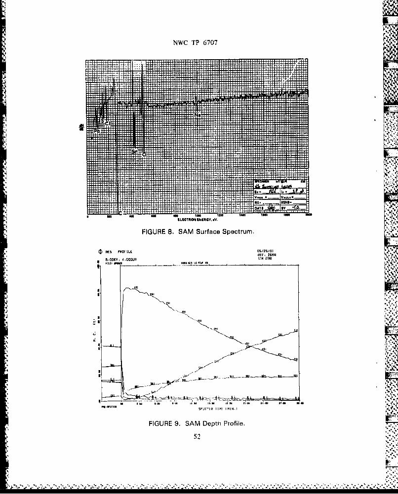
Scanning Auger Microscopy (SAM) is a sensitive surface analysis techniquewhich detects Auger electrons emitted from the outer 10 angstroms of a bombardedsurface. This allowed detection of surface contaminants such as unusually highlevels of organic material or oxides. Continuous elemental scans, coupled with siýmultaneous argon ion etching, provide informative depth profiles (composition ver-sus depth scans). Figure 8 represents a typical surface elemental scan whereas Fig-ure 9 shows atomic concentrations versus sputter time (depth). Depth profilingprovided information on the depth of diffusion and on contaminants within or underplated layers.
The first result of the metallurgical study was a listing (Table 1) of routinelysupplied, component lead protective finishes.
The mix of component lead finishes was no surprise once the applicable mili-tary specifications were studied. Table 2, which lists some of the capacitor, resistor, tA.and semiconductor specifications, highlights the fact that almost any coating can beused on a given device and certainly any quality of coating is allowed. Twonoteworthy exceptions to this lack of quality were discovered. They are Mil-M-38510for microelectronics and Mil-Std-1276 for electronic component leads. Mil-Std-1276 isparticularly attractive and M&PE will work toward upgrading this standard andhaving the improved version incorporated by more component specifications.
51 ,2.?
..... ~ ,...,.. ,., * .* . . -- ~* . . . *- .***~ *W* * * . *~ h~~
4'h'.,. .
NWC TP 6707
* tH ~4 ....... ... 3*~~~+- o mem em loe -1171mje
....A~ .............
FIGURE 8. AM.Surf.c.Sp.ctrum... ..........
.... . 1A0
+sus
~.OOKV.4.av4+. ~ ~ ~ ~ ~ ~ ~ U .I .I .1 . .. .... M N
*~~~~~9 S. IH _____
I ~ s.
low loKLCRM KROI W. I*.
FIUE8 A ufc pcrm
(D RE PRCILL 0626)0
".3U~KY 26149- H
FRO 0"
- C
1 O
I1A E WI I MIN.
FIGURE 9. SAM Depth Profile.
52

NWC TP 6707
TABLE 1. Protective Finishes As-Received from Manufarturers.
Thick tin or tin-lead (electrodepooited) over copper, nickel, (nickelsubstrates ranged from clectrodeposited to electroless to the wire itself, oriron-nickel.
Thin tin or tin-lead (electrodeposited) over copper, nickel, or iron-nickel.
Thick tin or tin-lead (hot dip or reflowed) over copper, nickel, or iron-nickel.
Thin tin or tin-lead (hot dip or reflowed) over copper, nickel, or iron-nickel,
Gold flash (leas than 8 microinches thick) over nickel or iron-nickel.
Thin gold (less than 50 microinches thick) over nickel or iron-nickel alloy. *
Gold (more than 50 microinches thick) over nickel or iron-nickel.
Silver over copper, nickel, or iron-nickel.
Lead over copper, nickel, or iron-nickel.
Zinc over copper,
Results from the 39 failure analyses combined with M&PE's experience allow-ed solderability failures to be categorized into the eight causes or modes listed inTable 3. Recommended general techniques for enhancing solderability are alsolisted. Failure analysis for solderability is now a very routine operation inHoneywell's M&PE labs.
These failure modes highlight the perishable nature of normal coatings. A ma-jority of the problems were due to solid state diffusion between the coating and thesubstrate or environmental degradation of the coating's exterior,
As an additional benefit from the metallurgical study, M&PE was able to de-termine the superior protective finishes for providing long-term solderability. Thefinishes in Table 4 have become the basis for callouts on Honeywell purchase orders.
M&PE plated numerous test pieces and tested various accelerated aging and -instrumented solderability techniques. The results of accelerated aging allowed usto rate Mil-Std-331 temperature and humidity cycling (28 days) as most severe, dryheat aging (16 hours at 1560C) as severe, IPC's 20- to 24-hour steam aging as op-timum, and Mil-Std-202, Method 208, as insufficient. It was obvious that the mili-tary's move toward increasing Method 208's aging length to 16 hours will be an im-provement. The results of using a laboratory-built surface wetting balance showedthe promise of objective solderability testing but also revealed several shortcomingsin both our in-house and the commercial instrumentation.
53
$3 ',12

NWC TP 6707
TABLE 2. Military-Specified "Protective Finishes."
Terminal Material Finish Spec/Component Type/Spec and Finish Callouta Thickness Requirements
Ceramic capacitor:Mil-C*20 None None/NoneMil-C-20/35 None None/NoneMil.C.39014 None None/NoneMil-C-39014/24 None None/NoneMil-C*11015 "Terminals shall be coated with None/None
solder having a 40 to 70% tincontent."
Mil-C.1101519 None None/NoneI Plastic capacitor:Mil-C -55514 "Terminals: Solid conductor None/None
suitably treated to f'ncilltatesoldering. When i,..oatingcontaining tin is ubad, the tinshall range between 40 and70%."
Mil-C-55514/2 None None/None
Supermetalized plastic film capacitor:Mil-C-83421 None None/None
Sm--841 alle oases: CSofdrcotd None/None
Variable,-ca stmersislr
Mil.R.94/47 Nonn Nnhson e/Nothne5Fixedd ion resistor:iche
%MSmall cses: None C fNone/None
Mil-R-.990/4 None None/None
Fixed, film resistor: 'I
Mil.R-89017 "Type C of Mil.Std.1276. Leads Nons/"Maximum coatingfree of non-conductive and thickness loes than twiceforeign materials." the minimum thickness ofr
any cross mection."Mil-R-89017/2 None None/None
Variable, wire-wound resistor:Mit-R.27208 "Terminals protected by a None/None
corrosion-resistant metalliccoating and suitably treated tofacilitate soldering."
Mil.R-27208/10 None None/NoneMil-R-39015 "Terminals suitably coated ta Nonie/None
meet solderabilityrequirements."
Mil-K-39015/1 None None/None %
54
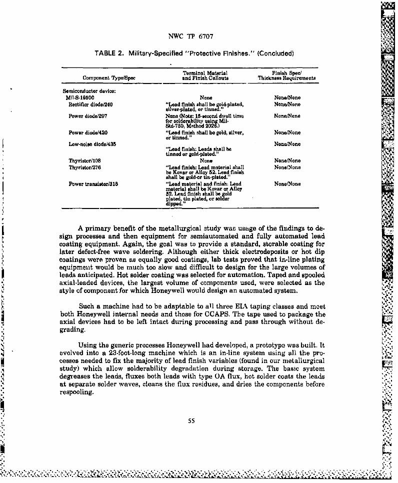
NWC TP 6707
TABLE 2. Military-Specified "Protective Finishes." (Concluded)
Terminal Material Finish SpedComponent Type/Spec and Finish Callouts Thickness Requirements
Semiconductor device:MRi-S-19500 None None/NoneRectifier diode/240 "Lead finish shall be gold.plated, None/None
silver-plated, or tinned."Power diode/297 None (Note: 15-second dwell time None/None
for oolderability using Mi1*Std.750, Method 2026.)
Power diode/420 "Lead finish shall be gold, silver, None/Noneor tinned."
Low-noise diode/435 None/None"Lead finish: Leads shall betinned or gold.plated."
Thyristor/108 None None/NoneThyristor/276 "Lead finish: Lead material shall None/None
be Kovar or Alloy 52, Lead finishshall be gold-or tin-plated,"
Power transistor/Si5 "Lead material and finishi Lead None/Nonematerial shall be Kovar or Alloy52, Lead finish shall be goldplated, tin plated, or aolderdipped."
A primary benefit of the metallurgical study was usage of the findings to de-sign processes and then equipment for semiautomated and fully automated leadcoating equipment. Again, the goal was to provide a standard, storable coating forlater defect-free wave soldering. Although either thick electrodeposits or hot dipcoatings were proven as equally good coatings, lab tests proved that in-line platingequipmeut would be much too slow and difficult to design for the large volumes ofleads anticipated. Hot solder coating was selected for automation. Taped and spooledaxial-leaded devices, the largest volume of components used, were selected as thestyle of component for which Honeywell would design an automated system.
Such a machine had to be adaptable to all three EIA taping classes and meetboth Honeywell internal needs and those for CCAPS. The tape used to package theaxial devices had to be left intact during processing and pass through without de-grading.
Using the generic processes Honeywell had developed, a prototype was built. Itevolved into a 23-foot-long machine which is an in-line system using all the pro-cesses needed to fix the majority of lead finish variables (found in our metallurgicalstudy) which allow solderability degradation during storage. The basic systemdegreases the leads, fluxes both leads with type OA flux, hot solder coats the leadsat separate solder waves, cleans the flux residues, and dries the components before ., .
respooling.
55

NWC TP 6707
TABLE 3. Soldering Failure Modes and Techniques for Restoration.
Failure Mode Restoration Technique
1) Mold release compound, oil, Surface cleaning; solvent, alkaline,grease, soil at surface fluorocarbon, or aqueous.
2) Zinc, lead, or lead-rich Strip or dissolve in molter, soldercoatings at high temperatures.
3) Contaminated tin or tin-lead Strip, overplate or hot solder dip.
4) Surface oxidation of tin or Brighten or hot solder dip.tin-lead
5) Thin, porous gold with Brighten, overplate, or hot solder dip.oxidized substrate
6) Thin, porous tin or tin-lead Brighten, overplate, or hot solder dip.with oxidized substrate
7) Thin tin or tin-lead with Strip, overplate, or hot colder dip.substrate diffused too nearsurface
8) Soluble plating over Strip and activate or overplate.S, nonsoldsrable substrate
TABLE 4. Component Lead Finish Requirements.
Resistor Family (copper or copper alloy leads)
Finish I: Matte tin.lead 300 to 600 microinches.
Finish II: Hot dip tin-lead (Sn60.63) 60 microinches minimum andwell wet with minimal time at temperature.
Finish MI: Matte tin o00 to 600 microinches.
Transistor/Diode/IC Family (iron-nickel alloy or Kovar leads)
Finish IV: Pure gold 50 to 100 microinches over 100 microinchesnickel minimum.
Finish V: Matte tin 300 to 600 microinches over 100 microinchesnickel minimum (tin must be reflowed if Mil.M-38510part).
Finish VI: Matte tin-lead 800 to 600 microinches over 100 micro-inches nickel minimi,m.
Finish VII: Hot dip tin-lead (Sn6u-68) 60 microinches minimum andwell wet over nickel 100 microinchas minimum. Minimaltime at temperature during hot dipping,
56
S~..

NWC TP 6707
To assure Honeywell and the NWC's Soldering Technology Branch that com-ponents were not degraded by the process, an electrical and cleanliness test plan wasdevised jointly. Honeywell performed the testing which proved that our specific ma-chine yielded an acceptable product and that our quality control testing was ade-quate for Honeywell use. This was finished in December 1985 and the machine hasprocessed over 1.25 million components for a production contract at up to 20,000components per hour. The theoretical limitation of a single type of component is -
32,000 units per hour. *
This process provides a standard, repeatable finish for EIA classes I, II, and IIItaped components. It provides in-line cleaning and drying in an optimized timeframe. It eliminates costly, error-prone, and sometimes dangerous, manual dipping.Thus, Honeywell has achieved its goal of providing a standardized, storable lead fin-ish on the largest group of components (axial, taped styles) to our optimized wavesoldering process. Coupled with M&PE's efforts in circuit board solderability, thiswill allow wave soldering using type R or RMA fluxes and generation of zero defects.
Fundamental to the success of wave soldering at Honeywell is M&PE's in-depth metallurgical and chemical knowledge of the root causes of good and badsolderability. Because of this knowledge, Honeywell's procurement and qualitydepartments now have real specifications on protective finishes. M&PE can worktoward incorporating real requirements into the component specifications, ac-celerated aging can be upgraded, solderability test objectivity can be improved, andconstructive and detailed corrective actions can be provided to our suppliers. A realbonus has been the automation of a system to standardize finishes on our largestgroup of components.
* Tests ut NWC have niot yet been completed.
57
'. j ¶
I I I -- I i I " I [ " I" ' .. .. .. ..
NWC TP 6707
Murk Shireman is the Principal Metallurgist/Materialsand Process Engineer (Soldering Technologist) withHoneywell, lie earned a BS degree in Material Sciencefrom Northwestern University in 1977 and since thattime has been deeply involved in scientific studios of thecauses of good and bad soldering, electronic packaging,and vendor interfacing. His work earned him the
Honeywell Special Achievement Award in 1984 forsolving hand-soldering problems, and Honeywell's topscientific award-also in 1984 for soldering technology.He was the Honeywell Engineering Club's nominee for1985 "Young Engineer of the Year in Minnesota." In1985 he was allowed a U.S. patent for co-inventing anAutomatic Lead Tinner, which was selected as erie of the"Seven Engineering Wonders in Minnesota" in 1986.Mark is a member of the American Society for Metalsand is Membership Chairman for the InternationalMetallographic Society.
Address: lHoneywell, Inc.Defense Systems DivisionMN 11-1812, 600 Second St. N.E.Hopkins, MN 56343 .'•
58
1.A

WETTING BALANCE SOLDERABILITY TESTING OF ELECTRONICCOMPONENTS AT RECEIVING INSPECTION
byJ. Gordon Davy
Westinghouse Electric Corp.Columbia, MD
For a copy of this paper, please contact
J.Gordon Davy
Westinghouse Manufacturing Systemsand Technology Center
9200 Berger Rd,Columbia, MD 21045
59
¾

NWC TP 6707
J. Gordon Davy is Senior Manufacturing Engineer at theWestinghouse Manufacturing Systems and TechnologyCenter. His specialty areas since 1979 include Solderingand lIermiticity and ljoak Testing for electronicpackaging soldering. IIls goal of reaching routine, defect-free soldering of printed wiring assemblies involvesensuring good solderability, ensuring good processcontrol (including SQC), and providing good training forinspectors, In May of this year he will chair a symposiumon Finish, Solderability, and Shelf-Life of FE'lectronicComponent Leads for the Semiconductor Equipment and
Materials Institute, which will be held in San Mateo,California,
Address: Westinghouse Manufacturing Systemsand Technology Center9200 Berger Rd.Columbia, MD 21045
,'V
60

NWC TP 6707
COMPONENT LEAD SOLDERABILITY VERSUSARTIFICIAL STEAM-AGING
byR,. Wild
IBM CorporationFederal Systems Division
For a copy of this paper, please contact
R. N. WildIBM CorporationFederal Systems DivisionBodle Hill Rd.Owego, NY 13827
61
.~ ,',NA

IINWC TF 6707
QUALITY THROUGH TRAINING
by
Joseph SylvesterOrmi Training CorpCovina, California
ABSTRACT
Controlling the electronic manufacturing process is the "QualityInsurance Program." Factors to be considered are:
ProductPersonnelProcess
This paper addresses the training requirements for operatingpersonnel assigned to the manufacturing area. Having properlytrained operators will ensure producing reliable quality productsat a competitive cost. To effectively and efficiently train opera-tors, there are basic requirements which must be satisfied. Theyare:
1. Course Curriculum
2. Training Area Design
3. Instructor Selection
4. Training Program
5. Student Pre-screening
6. Student Stress Control
7. Recertification
8. Special Courses
COURSE CURRICULUM
The course curriculum can only be designed after a thoroughbasic skills needs assessment study has been conducted. Thisstudy will establish and answer the question, "What skills andknowledge must operators have to efficiently produce quality products?"
"Basic skills should be separated from the special skillstraining requirements to ensure having each student trained andtested to an accepted basic skills level.
63
PRMVOUU PAGEIS I.LANK bi
y•'• b" .

NWC TP 6707
Special skills training can be scheduled when student hasreceived job assignments on the production floor.
Basic skills requirements:
a) Mechanical assembly
b) Tool use and care
c) Hand wiring and soldering
d) Wave soldering
e) Inspection
f) Touch-up and rework
g) Electro-static discharge (ESD)
h) Orientation and good housekeeping
Some special skills requirements:
a) Cable fabrication
b) Jumper wires
c) Component identificationd) Engineering design changes
e) Printed wiring board repair
f) Surface mount technology
g) Process sheet reading
TRAINING AREA DESIGN
The training area should be designed to provide the studentwith "a feel" of what an actual production position will be like.The training area position should mirror the actual productionposition. Ergonomics, bicmechanics and human factors are primeconsiderations in the design of the training area.
Design factors:
a) Work station
b) Seating
c) Lighting
d) Heating/air conditioning
e) Tools and equipment
f) Audio/visuals
g) Materials
h) Quality documentation
64
"W7

NWC TP 6707
The training area should be isolated from regular productionnoise and pressures to allow the student to learn properly. Theconcept of quality can be taught much more effectively in a propertraining environment.
INSTRUCTOR SELECTION
The selection of the instructor is of primary importance as he
is the keystone to the success of the training program. The instruc-tor must have excellent communication skills to ensure havingeach student understand the information being presented. Theold adage still prevails -- "If a student hasn't learned, theteacher hasn't taught." The instructor must also have the re-quired manual skills allowing him to demonstrate the proper wiringand soldering methods and techniques.
TRAINING PROGRAM
A teaching plan must be developed from the course curriculum.The instructor must schedule his time to provide:
a) Lecture/AV presentations
b) Demonstration of methods and techniques
c) Students practicing methods and techniques
d) Students producing workmanship samples
Effective teaching has been predicated on the following axiomfor many years.
I HEAR ...... AND I FORGET.
I SEE. . . ... AND I REMEMBER.
I DO . . . . . AND I UNDERSTAND.
The course must be segmented into training modules, Thisallows students to learn skills in a build-on manner. The studentmust produce workmanship samples for each segment/module. Pro-ducing of workmanship samples can be used to promote decision
', making by the student. The instructor will evaluate the firstsamples and offer corrective recomnendations for the student'sbenefit. Al. subsequent samples will be evaluated by the student,who will compare the sample to a workmanship manual and make a work-manship assessment. The instructor then evaluates the student'squality assessment. He can then accept the sample or offer cor-rective recommendations. This student decision/instructor inter-face will prepare the student for actual quality decis.ons onthe production floor. This practice will definitely reduce touch-up and operator/inspection indecision on the production floor.
65
p, . .

NWC TP 6707
The practice of having students produce workmanship samplesfor each segment/module taught will provide the instructor/companya visible record of student's comprehension/skill level. Thecontinual assessment provides necessary data for determining stu-dent's progress. This data permits deciding whether:
a) Student's performance is satisfactory
b) Additional training is recommended
c) Student is not capable of performing assigned taskand should be reassigned or terminated
At the end of the course, each student must have a packageof approved workmanship samples for each module/segment.
A written test must also be taken by each student to measurecomprehension level of course material presented. The workmanshipsamples and the written test eventually become a permanent partof the student's employee file/record. Satisfactory completionof the training course should culminate in a formal presentationof completion certificate and a certification card duly authorizedby the instructor.
EMPLOYEE/STUDENT PRE-SCREENING
Pre-ocreening and testing of prospective applicants has be-come increasingly inportant. The "new electronics" utilizingmicro/macro componentry and high density packaging has introducednew requirements into our labor force.
Basic pre-screening requirements are:
a) Eyesight examinations
b) Language understanding
c) Comprehension testing
d) Acceptable manual dexteritye) Attitude (sparkle-in-the-eye)
STUDENT STRESS CONTROL
The instructor's primary concern is the transfer of knowledgeto the students. The best way to reduce stress in the trainingroom is to know your students. The more you know about them,the more you can understand the stresses they may be experiencing.The person may be out in the work force for the first time, outof necessity, or just wanting to work.
66

NWC TP 6707
You must consider the environment the student is coming fromand the new experiences the student is undergoing. The more under-standing given the student, the greater the response, resultingin a better employee.
Some factors the instructor should consider are the student's:
a) Background -- previous experience and training
b) Education
c) Present skills level
Stress considerations are also very important during thestudent's first interface with the production area. The studentnow interfaces with a new environment, actual production material,production effort (schedule), other employees (peers), and firstline supervision.
In spite of all of the above, it must be repeatedly conveyedto the student, as a prospective new employee, that performingquality work at the assigned tasks is an integral part of theoverall company work effort. Quality is a state of mind, not
just a production objective.
RECERTIFICATION
Recertification, or continual skills assessment on the manu-facturing floor, must be scheduled and controlled. The recerti-fication schedule must be established based on factors such as:
a) Quality level
b) Complexity
c) Criticalness
d) Cost
Recertification is a mandatory process in that operatorsquickly develop work shortcuts on the manufacturing floor that,in many instances, are in contradiction with time proven methodstaught in the classroom.
SPECIAL COURSES
INSPECTION TRAINING
Inspectors must be thoroughly familiar with the company'sworkmanship specification and workmanship manual. The reasonfor rejection of any solder connection or electronic hardwaremust be substantiated by the documents. This technique promotesrecognition of' all classic rejects by sight and thorough under-standing of the written criteria in the specification. This will
67
• •,r

NWC TP 6707
reduce touch-up and rework. The doctrine of acceptance basedon functionality, not aesthetics, must be pursued to reduce touch-up.
Inspectors must be trained by using actual samples or colorphotography criteýria showing exactly what is required. This meanspositive establishment of preferred, minimum, and maximum accep-tance criteria.
A formal inspection testing program must be designed andimplemented. Recertification of inspectors must be done on aregular basis to ensure uniformity of the insp7ction function.Continual retraining and assessment of inspection skills throughrecertification must be scheduled. This process will reduce inde-cision and opinion calls by inspectors which could result in costlyrework and/or possible scrapping of expensive electronic hardware.
Most successful companies have made the satisfactory comple-tion of the hand wiring and soldering course a prerequisite ofthe inspection course.
CONCLUSION
Cost effective production of quality products can only beachieved by proper selection and training of operators by quali-fied instrucro-r"sing industry accepted methods and trv: i~imaterials.
Additional information can be obtained from the author,
Joseph SylvesterOuii Training Corp20628 Arrow Highway, Suite 5Covina, CA 91724
J.
68
V.,______ . - . - * . . ' ., ~ ~ . * i •
, . . -i1 i -* • ! r I -,p-R - -•.-,prJ,__-______-__-_-.___. . l i l a - •_ _._m z i _. __ _ • l_/-.'• /,*... *.•a .. u •., • •~ d ,*

NWC TP 6707
Joseph Sylvester is President of OMNI Training Corp., atraining and consulting firm in Covina, California,where all phases of electronic assembly are taught. Hehas served as Director of the Technology LearningCenter in Garden Grove, and as Vice President ofResearch and Development and Technical Director ofboth Solder Removal Co. and Hexacon Electric Co.Previously he was a Staff Industrial Engineer for AllenB. Dumont Labs and Bendix Corp. Joe holds manypatents on tools and technical processes and has writtenfor the American Welding Society and Institute ofPrinted Circuits Handbooks, l-e received a degree inIndustrial Management from Fairleigh Dickinson
University and is a senior member of the Society ofManufacturing Engineers and the American Institute ofIndustrial Engineers, as well as a member of theAmerican Society for Training and Development.
Address: OMNI Training Corp.20628 Arrow Highway, Suite 5
I,
4,.!
4i
69
I.'.

NWC TP 6707
PROPOSED STANDARD FOR"MAGNIFYING POWER"
OF VISUAL MAGNIFICATION AID/DEVICESAND'
"HUGHES MAGNASCOPE"CALIBRATION INSTRUMENT DESCRIPTION AND USE
by
Donald J. StrittmatterAssistant Manager, Design & Analysis Operations
Missile Operations Division, Hughes Aircraft CompanyTucson, Arizona
'I'
ABSTRACT
PROBLEM: Many magnification aids have magnifying power values advertised, specified,and stamped on them, but it seems that almost everything but standard microscopes are incorrectlymarked and do not conform to any recognized optical equation for determining magnifying power.We found almost all 4X inspection devices ran from 0.8X to 3X, and 10X devices ran from 5.6Xto 11X; also three very complex, very expensive instruments were all about one-half their markedvalue.
HAND HELD SOLUTION: Because of this, Hughes has designed and built special wide-angle, low distortion, high resolution, long-working distance, 4X and 10X magnifiers mounted inthe center of fiber optics ring lights which are hand held or mounted on a swivel-swing arm stand.
ADVANCED INSTRUMENT SOLUTION: Hughes has also designed and is building aspecial "Optical Semiautomatic Inspection Station." This new system utilizes a stereo head-up displaywith large pupils, long eye relief, wide field, high resolution, coplanar objects, optimized toe-inand eye focus distance, is computer driven, and features low fatigue, and fast operating concepts.
UNIVERSAL STANDARD DEFINITION: The magnification aid industry has not usedrecognized, truly universal definition or method of measuring magnifying power that works with .
any type of simple or complex magnification device. Hughes has selected and herein proposes astandard definition which allows a fast and easy method of measuring quickly and on-the-spot themagnifying power (MP) of any visual magnification aid as a device.
HUGHES MAGNASCGPE: To work in conjunction with the standard definition of MP,Hughes has developed the "HUGHES MAGNASCOPE," This instrument's selection, calibration,and use is described in detail.
71 •
PREIv'OUS PAG-E,_IS 1LA.'K
*""i",'%-

NWC TP 6707
PROBLEM
Magnification aids have magnifying power values advertised, specified, and stamped on them,
but it seems that almost everything but standard and zoom micvoscopes are incorrectly markedand do not conform to any recognized optical equation for determining magnifying power.
MAGNIFYING DEVICES SURVEY
We found that, after testing over 10 different 4X devices, almost all of them ran from O.AXto 3X, and that 1OX devices ran from 5.6X to lX. Also three very complex, very expensive in-struments were all about one-half their stated values. Because of these results, it is recommendedthat the inspection community should measure and certify all magnifying inspection devices inuse and before placing any new ones in use.
Quick Hardware Solution At Hughes
Since the only devices that measured cnrtectly had very small fields of view and poor resolu-tion, Hughes designed and built special wide-angle, low distortion, high resolution, long-workingdistance, 4X and 10X magnifiers mounted in the center of fiber optics ring lights which can behand held or mounted on a swivel-swing arm stand. Figures I and 2 show this inspection station.
V, ,.
FIGURE 1. Hughes 4X/1OX Swivel-Swing Arm or Handhe!d Magnlf~erwith Fiber Optics Ring Light Inspection Station
72
-J%

NWC TP 6707
737
ý'L* -A N-
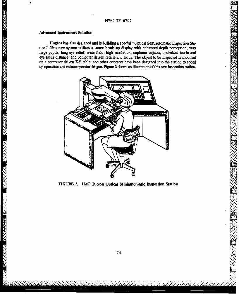
NWC TP 6707
Advanced Instrument Solution
Hughes has also designed and is building a special "Optical Semiautomatic Inspection Sta-tion"' This new system utilizes a stereo heads-up display with enhanced depth perception, verylarge pupils, long eye relief, wide field, high resolution, coplanar objects, optimized toe.in andeye focus distance, and computer driven reticle and focus. The object to be inspected is mountedon a computer driven X-Y table, and other concepts have been designed into the station to speedup operation and reduce operator fatigue. Figure 3 shows an illustration of this new inspection station.
FIGURE 3. HAC Tucson Optical Semiautomatic Inspection Station
, 774 ¢:
J''E.*.4.,;*'.* ' ,-. .-. , ... i I .. * . .

NWC TP 6707
UNIVERSAL DEFINITION NEED
The magnification aid industry has not used a recognized, truly universal equation, defini-tion, or method of measuring magnifying power that works with all types of simple or complexmagnification devices. Also, the more complex the magnifying device, the more difficult it is tomeasure real magnifying power. There are many equations and many ways to interpret their use.The more general equations use eye relief, lens spacings, and user's eye near or far focus condi-tions. The operator's contribution to system magnification is zero if his eye is focused at its far-point, infinity; however, if the operator's eye is 'bcused at its near point of 10 inches, system magnifica-tion is one plus the magnifier aid's value, This leads to confusion about whether the magnifyingpower should be measured for the device or ar. system magnifying power that includes the operator'scontribution to magnification.
Since it is desirable to define one standard method and since the condition of the operator'seye focus is not easily controllable or certifiable, its effects should be eliminated from definitionsor measurements of magnifying power. Therefore, when defining magnifying power, the operator'seye should be defined as focused at infinity so it has no effect on measuring the magnifying powerof the device. This can result in magnification device specifications that are measurable and certifiable.
In order to end confusion and give one standard definition with a simple method of using 4..it, this paper proposes a single standard definition with relative tolerances and an example of afast and easy method of measuring on-the-spot magnifyiag power (MP) of any type of visual aiddevice.
75 ," ,'I

NWC TP 6707
PROPOSED STANDARD DEFINITION FOR MAGNIFYING POWER (MP)
The apparent size of an objet viewed with the eye is dependent upon the size of image formedinside the eye on the retina. This Image size is directly related to the angle subtended by the objectat the eye (see Figure 4),
C B A
FIGURE 4. Image Size Increase vs Object Closeness
As an object is brought closer to the eye, it subtends a larger angle and forms a lareger' image
on the retina. The eye, however, is limited in its ability to focus on near objects. The "average"observer cannot focus sharply on objects closer than 10 inches from the eye. This is referred toas the near point of the eye and defined as unity magnifying power.
If a magnifier (positive or convex lens) is placed in front of the eye, the effective near point
is moved closer to the eye, thus increasing the subtended angle and therefore the size of the retinalimage (see Figure 5). The size of this "magnified" image is compared to the size of the imagewhen viewed at the near point with the unaided eye to give the "magnifying power" of the magnifier
device.
0 AXI S V
10 INCHES
CL AXIS _
S'.- I0 INCHES
FIGURE 5. Image Size Increase with Magnifier Use
76

NWC TP 6707
For example, if the image is two times the size of the image with the unaided eye viewedat 10 inches distance, the power is "2X."
The height of the retinal image is proportional to the tangent of the angle subtended and,in general, magnification or magnifying power is definod as the ratio of these retinal image heights.
.The following is a proposed universal standard definition for magnifying power of any typeof visual aid device. It was derived by combining equations and definitions from Section 7 of MIL-HDBK-141, MILITARY STANDARDIZATION HANDBOOK/OPTICAL DESIGN.
MAGNIFYING POWER (MP)
The magnifying power "MP" for a visual magnification aid/device shall be determined withthe device focused so its image appears at infinity and by using the equation
MP- Tangent 6lMP- -- ngent• 0
where 6 shall be one-half the angle subtended by the image H' of an object H as seen throughand centered in the field of view of the magnification aid!device, Q shall be one-half the anglesubtended by the object H as seen at 10 inches by the unaided eye, and Tangent 1: equals 1/2 Hmeasured in inches divided by 10.
Figure 6 illustrates the relationship between B, 0, and H', and H.
0 2H OBJECTHUNAIDED
10 INCHES --
CENTERED IMAGEOF THE OBJECTSEEN THROUG4IH
/ - AIDg/DEVICE
.MAGNIFICATION AID/DEVICEFOCUSED AT INFINITY
FIGURE 6. ir
77•. *%-*2*% .k
NWC TP 6707
With magnifying power (MP) defined, a functional, realistic MP tolerance should also beconsidered. This will allow manufacturers of magnifier devices, specification writers, and qualitycalibration activities to all work toward a common functional goal.
The following realistic functional tolerances are proposed:
1) Magnifiers with a MP of 4X to 25X should be manufactured such that MP is controlledto ±10%.
2) Specifications that call out MP requirements that have to be measured and certified shouldspecify the required MP with a tolerance of -ý 15%. For example, "Solder joints shall
be inspect'-4 with a device that produces a magnifying power of 10 ± 15%.
3) Calibration instrumentation and procedures used to measure MP of a magnifier shall becapable of accuracies better than ± 4%.
4) For magnifiers with an MP of less than 4.00, the above tolerances should be doubled.
78
. I . . . .. .

NWC TP 6707
MEASURING METHOD
This paper proposes a simple method that is fasL to use once a reference angle measuringinstrument is constructed and calibrated. The following describes how to choose this instrument,how to calibrate it, and how to use it to measure magnifying power of any visual aid used to addmagnification to the naked eye.
For the rest of this discussion, this magnifying power measuring instrument shall be refer-red to as the "HUGHES Magnascope."
Basically, the "HUGHES Magnascope" is a telescope that is focused at Infinity and that
contains a calibrated 1/2 field angle reticle. When used to view through a magnifier device undertest, an observer can make a reading of a measuring scale and perform a simple calculation todetermine magnifying power. The "HUGHES Magnascope" may also be used in conjunction withspecially calibrated "Object Target Scale" and measure magnifying power with a direct reading.
SELECTION OF MEASURING INSTRUMENT TO BE MADE INTO A "HUGHESMAGNASCOPE"
An instrument must be made or selected that can be calibrated and can be easily used tomeasure 8 (the 1/2-angle subtended by the image of an object seen through the magnifier). Selecta small low-power telescope with a symmetrical reticle target pattern that can be calibrated fora 1/2-field angle. The telescope eyepiece must be focusable to the reticle, and the telescope objec-tive lens must be focused at infinity, or focusable to infinity so that the "HUGHES Magnascope•'will be used to measure the magnifier's infinity-tbcused image. Also, the objective lens of the telescopemust be capable of being apertured down to 4 to 5 mm diameter to simulate the eye's pupil size.
Telescopes of this type are called alignment telescopes, or autocollimators. A very compact,reasonably priced, and handy-to-use telescopc that might be considered is the "#14 Walters 8 x30 Monocular With Grid" that comes with a usable target reticle already focused at infinity,
S. Walters, Inc.32208 Oakshore Drive .,.
Westlake Village, CA 91361 .
Phone (818) 706-2202 7--"71
* . CALIBRATION FOR TANGENT (13 MAGNASCOPE)
After selection of the telescope to be made into a "HUGHES Magnascope," standard op-tical instrumentation methods of autocollornating may be used to position the reticle at the infinityfocus of the objective. If this is not convenient, a telescope already fbcused at infinity may bepurchased.
79
. , ......- ............

NWC TP 6707
Next, a 4 to 5 mm diameter aperture must be placed in front of the telescope's objectivelens. This simulates ýhe observer's eye pupil size when measuring magnifiers later and also reducesparallax errors when calibrating the "HUGHES Magnascope:' If using the Walters monocular,the lens cap for the objective that comes with the monocular may be used by placing a hole inits center and placing it on the monocular.
With the telescope objective lens focused at infinity, the eyepiece shall be focused on itsreticle while viewing a yardstick 2000 inches away from the objective lens of the telescope, Measure(1/2 H Magnascope) the distance subtended from the center of the reticle of the telescope to themark chosen on the reticle pattern you want to calibrate for lTngent (B Magnascope). An easyway to measure this distance is to use two light-colored pencils as markers for the yardstick thatis placed against a dark-colored background. Place one pencil perpendicular to and at the startof the yardstick. Position the telescope so the center of its (B Magnascope) reticle pattern is alignedwith the pencil at the start of the yardstick. Then move the second pencil out along the yardstickuntil it .3 in alignment with the mark on the (B Magnascope) reticle pattern to be calibrated. Thisdistance is (1/2 H Magnascope) measured in inches, See Figure 7.
..-- YARDSTICK 2000 INCHESFROM HUGHES MAGNASCOPE -PENCIL
""(I/H MAGNASCOPE)
S( ,BMAGNASCOPE)
(H MACNASCOPE)
HUCHES MAGNASCOPEFOCUSED AT INFINITY--
(B MAGNASCOPE) RETICLEPATTERN TO BE CALIBRATED
FIGURE 7.
80
III lie

NWC TP 6707
If you arc using the Waiters 8 x 30 monocular for your "HUGHES Magnascope," measurethe distance from the center of the reticle to the mark defined by #1 which defines the locationof the tenth mark from the center (see Figure 8),
2I I 2
(. 2H MAGNASCOPE)SUBTENDED ANGLE AND
(J MAGNASCOPE) RETICLE PATTERN
FIGURE Walters Monocular Reticle
As a rough guide, the distance (1/2 H Magnascope) for the Walters monocular is about 25
inches. However, remember, because of manufacturing tolerance for reticles and for objective lensfocal length of the monocular, each Walters monocular has to be calibrated individually for (1/2H MaSnascope). Values in this paper should only be used as reference examples.
Now that (1/2 H Magnascope) is known, Tangent (B Magnascope) can be calculated usingthe following equation:
(1/2 H Magnascope) (2)Tangent (B Magnascope) = H
Magnascope to Object Distance
Tangent (II Magnascope) = (1/2 H Magnascope) measured in inches2000
iLe.: Tangent (8 Magnascope-Walters Monocular) 2 00 0.01252000."
This finishes calibration of the "HUGHES Magnascope" for Tangent (B Magnascope). Now ,?.'..'the magnascope can be used to measure (1/2 H Magnifier) that is needed to calculate Tangent aused in calculating magnifying power of a magnifier device.
814:::::

NWC TP 6707
DETERMINING (TANGENT a) USINGTHE CALIBRATED "HUGHES MAGNASCOPE"
Recall from the definition of magnifying power, B equals 1/2 the angle subtended by the
image H' of the object H as seen through the magnifier and a equals 1/2 the angle subtendedby the object H as seen at 10 inches by the unaided eye. Also recall
Taingent a = 1/2 H measured in inches10
or
(1/2 H magnifier) measured in inches (3)Tangent C7 ffi
where (1/2 H magnifier) is defined as the object size subtended by the (8 magnascope) reticle pat-
tern when looking through a magnifier under test with the "HUGHES Magnascope,"
To measure (1/2 H magnifier) the following steps should be performed:
1) The calibrated "HUGHES Magnascope" should have its eyepiece focused so that the reticleimage is sharp. The 4 to 5 mm diameter aperture should be in front of the telescope'sobjective lens to simulate the observer's eye pupil size,
2) Using the magnification aid to be tested, a finely divided ruler or scale is observed andfocused on with its edge in the center of the magnifier's field of view,
Note: A 0.1 inch linear scale geaticule with 100 divisions of 0.001 inch increments workswell with the Walters Monocular. This scale is stocked as part number 11-8703 by Ealing,Pleasant Street, South Natick, MA 01760, phone (617) 655-7000 or by part number 70.0166by Rolyn Optics Company, 738 Arrow Grand Circle, Covina, CA 91722-2199, phone (818)915-570"7, '
3) The location of the user's eye relative to the magnifier aid in use should be noted. The"HUGHES" Magnascope's" objective lens should be located in the same relative loca- ..tion with respect to the magnifier aid as that which the eye was in while using the magnifieraid. It is desirable to use a holding fixture to keep the "HUGHES Magnascope" firmlypositioned relative to the magnifier under test.
4) The Magnifier Aid and the "HUGHES Magnascope's" relative spacing must be fixedand focused on the scale by moving them as one, together, toward and away from thescale. Again, a holding fixture is desirable to accomplish this focus.
5) With the "HUGHES Magnascope's" reticle center aligned at the starting edge of the scale,measure (1/2 H Magnifier) the distance subtended on the scale by the (I1 Magnascope)reticle pattern calibrated earlier.
82
'S6S4*~

NWC TP 6707
When measuring a 10 power magnifier using the Walters monocular, the (B Magnascope)reticle pattern calibrated was 10 units firom center and that mark subtends a (1/2 H Magnifier) scaledistance of approximately 0.0125 inches.
Now that (1/2 H Magnifier) is known, Tangent a can be determined from equation (3).
T (1/2 H Magnifier) mcasured in inchesTangent (a Walters mc'iocular) 1010
0.0125- 10 = 000125
I-
, o..•..o
101
83

NWC TP 6707
CALCULATION OF MAGNIFYING POWER
Now that Tangent (15 Magnascope), (1/2 H Magnifier), and Tahngent a are known, magnify-ing power of the mag'fication aid can be calculated using equations I and 3.
MP =Tangent 0Tangent a
MP Tangent (B Magnascope) (4)(1/2 H Magnifier)
10With the Waiters monocular calibrated "HUGHES Magnascope" measuring a 10 power
magnifier aid/device, MP calculates to be the following:
¢.v 25-- 2000
MP 0.0125
MP - 10
Now that this calculation has been made to show how MP is calculated, and a "HUGHESMagnascope" has been made by calibrating the Walters monocular for Tangent (B Magnascope),equation 4 for the calibrated instrument can be simplified as follows.
MP aTangent (8 Magnascope)(1/2 H Magnifier)
10
MP 10 x Tangent (B Magnascope) (5) ,'
(1/2 H Magnifier)
i.e.: 10 x 2""MP 712 H Magnifier)
MP= 0.125 (6) II(1/2 H Magnifier)
Therefore, now that the "HUGHES Mcgnascope" Walters Monocular is calibrated to get•m magnifying power, all that is required is to divide the scale distance reading seen through any visual
magnifier device that is defined by the collimated reticle marks into 0.125. Remember, each instru-nment must be calibrated and these are only reference values in the paper.
84
'." * f ., C W ,
.7

NWC TP 6707 ,•'
DIRECT READING MP MEASURING INSTRUMENT
A direct reading MP measuring "HUGHES Magnascope" can be made that requires nocalculations. This can be done if a special reticle is designed and made for the "HUGHESMagnascope" to compliment a specially made "Object Target Scale" to be looked at through theMagnifier Aid.
A telescope similar to the #14 Waiters 8 x 30 Monocular with Grid could again be usedfor the direct reading "HUGHES Magnascope."
If the #14 Walters monocular is used, its reticle has a center mark with 25 markings goingout from each side of center. Define each unit of these 25 divisions as one power. This will allowmeasurement of up to 25 MP with this reticle. Tb use this reticle pattern, (1/2 H Magnascope)is nmeasured for the reticle distance from the center to the 10 mark and Tangent (B Magnascope)is calculated the same way as described in the Measuring Methods section of this paper.
Recall from equation 2 that Thngent (BI Magnascope) for the Walters monocular calibrated"HUGHES Magnascope" was the tollowing;
Tangent (B Magnascope-Walters Monocular) = 0,0125
To define the spacings for construction of the special "Object Target Scale" that will be used,',for viewing at through the magnifier aid under test, equation 4 is used:
MP = 'bhngent (3 Magnascope)(1/2 H Magnifier)
10
Now solving for (1/2 H Magnifier)
10 x 'fhngent (11 Magnascope) (7)(1/2 H Magnifier) = MP
For the Walters monocular calibrated "HUGHES Magnascope" looking through a 10 powermagnifier aid:
25 (8)10 x, ',
(1/2 I-I Magnifier-Walters Monocular) = 0.0125I0
85'. .
.. . . . .. . * .~*a ,*..

NWC TP 6707
Note: (1/2 H Magnifier-Walters Monocular) comes out to be the same "Object Target Scale"size for use with all MP values. Therefore, all that is necessary is to make one special "ObjectThrget Scale" for use in measuring any device up to 25 MP when using the Walters Monocular.Figure 9 shows a typical "Object Target Scale:'
I-I
p.' 7 -(V 2 H MAGNASCOPE)
FIGURE 9. Direct Reading NP Special Object Target Scale
In use, the center of the "HUGHES Magnascope's" reticle is aligned with one edge markon the special "Object Target Scale." Then the MP is read from the "HUGHES Magnascope"reticle's intersection with the opposite end mark of the "Object Target Scale."
Figure 10 shows what would be seen when measuring a 10X magnifier aid/device.
2
FIGURE 10. Direct Reading HUGHES Magnascope of a 10X Device
86
A. 1 I°r.
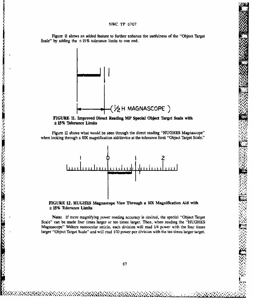
NWC TP 6707
Figure 11 shows an added feature to further enhance the usefulness of the "Object TargetScale" by adding the + 15 % tolerance limits to one end.
._.a.
FUV. H MAGNASCOPE ?FIGURE 1% . Improved Direct Reading MP Special Object Target Scale withE 15% Tolerance Limits
Figure 12 shows what would be seen through the direct reading "HUGHES Magnascope"when looking through a lOX magnification aid/device at the tolerance limit "Object Target Scale."
4,I I
FIGURE 12. HUGHES Magnascope View Through a 10X Magnification Aid with+t 15% Tolerance Limits :
Note: If more magnifying power reading accuracy is desired, the special "Object Target ::*
Scale" can be made four times larger or ten times larger. Then, when reading the "HUGHESMagnascope" Walters monocular reticle, each division will read 1/4 power with the four timeslarger "Object Target Scale" and will read 1/10 power per division with the ten times larger target.
87 ""
4, .'-5'...• £
i•, . ".:_'.(.'•.,•.:(•'•,'•. ... ,, ., ,,• • ,o."• ,, ,.',,•,•,.•.: : ,..•,.% ,,.,.:., •. .. •, .•,... . "'

AVV
4 NWC TP 6707
Figure 13, 14, and 15 show the "HUGHES Magnascope" in use on a fluorescent ring light
magnifier, a bench magnifier, and the HUGHES swivel 4X/1OX Inspection Station.
I,N
A'~' 4,0
....... ......
j A44%
FIUE1."UHSMgacoeITsigAIorsen igLgtMgiir.
,., p. 88

4,'4�
NWC TP 6707 it
'� S.(4my
I *'�§�'
we
wL
L..S FIGURE 14. "HUGHES Magnascope" 'kiting A Bench Magnifier .
li I,'I'
.4,'
N.'
N->
I..,,
4'4
894.I!.
U,
* 4e '.�.L *��.'h*-". �,� . . . . C C. *P,. - C 4
4. * .C

NWC TP 6707
FIGURE 15. "HUGHES Magnascope" Te~sting A Hughes 4XtIO Swivel-Am Magnifer Station
90a
NWC TP 6707
Donald Strittmetter has 27 yeara experience in Electro-Optics
and Optical
Instrumnentation design.
with Hughos
Aircraft Co. where he is Assistant Manager of Designand Analysis Operations.
Address: Hughes Aircraft Co.Bldg. 802, Mail Station 1P.O. Box 11337
*Tucson, AZ 85734
7%
m!
91
W '
S...
''
n
n
i
n I
II
i4

NWC TP 6707
SURFACE MOUNTED DEVICES-FACTORSAFFECTING THE ADHESIVE PROPERTIES OF
SYNTHETIC AND ROSIN-BASED SOLDER CREAMS
Norman MabLeod
andLarry Hoover
Federated-Fry Metals, Inc.6th Avenue and 41st StreetAltoona, PA 16602
For a copy of this paper, please contact
Norman MacLeodFederated-Fry Metals, Inc,6th Avenue and 41st StreetAltoona, PA 16602
r
S.. ..,
VIOUS PAGE
93 ,S BLANK
, %
S'k

NWC TP 6707
Surface Mounted Devices.
Factors Affecting The Adhesive PropertiesOf Synthetic And Rosin-Based Solder Creams
Solder creams are mixtures of solder powder, flux, solvents andvarious other compounds blended in varying proportions to givethe properties required for different end-uses. As with mostproducts, the final result is a balance of properties, some beingobtained at the expense of others.
In many creams, it has been apparent that good screen printingor dispensing characteristics have been obtained at the expenseof tackiness. However, in many operations involving surfacemount technology, no adhesive is used, the tackiness of the creambeing ,he a,-ee- means of holding devices in place, in accurate align-ment, between the assembly and the solder reflow arbas.
To measure the adhesive properties of creams, a simple device hasbeen developed from equipment available in most laboratories. Thishas been used to assess the effects of film thickness, solvent com-position, rosin content, metal loading and other factors on deviceadhesion and other properties such as drying time. The interdepen-dence of these factors has also been assessed to ullow for betteroptimisation of the compet!., prformance requirements.
().j
NWC TP 6707
Norman MacLeod, a Scotsman born in England, holds anhonours degree in Organic Chemistry from the Universityof Nottingham. He has worked on a variety of subjects forthe British Petroleum Company Research Centre, and hasdone extensive R&D in polymers for the Cookaon Group.His work with the Research Department of Fry's Metals inLondon was on photosensitive coatings for printing plates,with an Interest in flux chemistry and particularly the clean-ing of flux residues. His work with Federated-Fry Metalshas him commuting between the USA and England.
Address: Federated-Fry Metals Inc.6th Avenue and 41st StreetAltoona, PA 16602
95%
95 '.,. -'
,- .'. •v
• a '-i° %

NWC TP 6707
Larry Hoover was graduated from the Williamsport Area
Community College with an associate degree inElectrical Technology. He attended the University ofPittsburgh studying Electrical Engineering whileemployed by Bethlehem Steel and later U.S. Steel. Since1982 he has been Department Head and TechnicalRepresentative for the manufacture of solder powdersand flux.
Address: Federated-Fry Metals Inc.6th Avenure and 41st StreetAltoona, PA 16602
9.
96 """-
LI

NWC TP 6707AUTOMATED INSPECTION OF SURFACE MOUNTED SOLDER CONNECTIONS
A STATUS REPORT ON A FIRST INSTALLATION
byMike Juha
Manager of ProductsIRT Corporation
San Diego, California
ABSTRACT
The acceptance of surface mounting in the electronics industry hasbeen slowed by problems with component availability, electricaltesting, and inspection.. Industry suppliers and users have beenworking to solve these problems, and these problems are easing.Component manufacturers are offering substantially more devices in
surface mountable packages.. Automated test equipment vendors areoffering test fixtures for surface mount circuit boards. And justrecently, solder connection inspection has been automated through a"partnership" effort with a major electronics manufacturer. The resultachieved in this successful first installation is the subject of thispaper$
THE NEED FOR SOLDER QUALITY INSPECTION
Surface mounted devices are held in place on the circuit board bytheir solder connections. The same situation occurs onplated-thru-hole circuit boards. However, with surface mounting, thereis no solder plug surrounding a pin thru a hole in the circuit board togive the connection added strength. Instead, the solder alone bondsthe device to the circuit board, as shown in Exhibit 1. The electricalintegrity of the circuit board is totally dependent upon the structuralintegrity of the solder connection. This issue of structuralintegrity, plus the large numbers of solder connections on each circuitboard, are the impetus for automating solder connection inspection.
Surface mounting makes more electronic products man-portable ormobile in vehicles. With this portability or vehicular mobility comesshook, vibration, and extremes of temperature. Shook, vibration, andtemperature approach or exceed levels that were previously associatedonly with military electronics. These higher stress levels must besustained by the smaller solder connections characteristic of surfacemounting. Numerous experts have cited how surface mounted solderconnections are disposed to fatigue and creep failure.
97
N..J

NWC TP 6707
STRESS AND ELECTRICAL TESTING
The structural integrity of solder connections can be assessed tosome degree with "shake and bake" stress testing. However, this typeof testing confronts the risk of wearing out the product before it everreaches the custorer. Further, the electrical testing that is used
with "shake and bake", as well as that usually performed in regularmanufacturing quality assurance, detects only the "open" or "short"conditions. Stress testing typically does not expose the structurallymarginal connections that still conduct, but are long term candidates 4
for failure, such as: 'U"
o Insufficient solder; I•o poor wetting;o excess solder or lead projection;o device or lead off position;o unwanted solder balls or splashes;o device tilted relative to the board;o porosity in the solder connection..'•
VISUAL INSPECTION
Visual inspection can detect gross defects, such as missingdevices, bridges outside the devices, the absence of solder fillets,and non-wetting, However, visual inspection is qualitative rather thanquantitative---it does not measure the extent to which a defect exists.Also, visual inspection relies upon the external appearance of thesolder connection to infer its internal structural integrity. And withsurface mounting, the solder connections are partially or fullyunderneath the devices, making visual inspection impractical.
STRUCTURAL INSPECTION
Structural inspection is not a new problem. For years, aerospace*" and casting manufacturers have used X-ray inspection to examine the
structural integrity of castings for airframes, engines, andtransmissions. Since solder connections are a "casting" formed by thesurface tension of the molten solder and the surfaces of the device andthe circuit board, X-ray techniques will work for solder connections.The keys to making X-ray techniques viable for solder connectioninspection are to:
1speed up the X-ray imaging process,2 radiation from damaging electronic components,3 improve X-ray imaging to resolve 0.001 inch features,3 automate inspection to achieve fast, accurate results, and4 make the techniques usable in the production line.
98St.%
S r ,. - . - 4 4

NWC TP 6707
DEVELOPING A SOLDER QUALITY INSPECTION MACHINE
In 1984, we became aware of the need for structural inspection of'solder connections in surface mounted electronics thru a customer, anddeveloped the machine shown in Exhibit 2 specifically for solderconnection inspection. This machine took "flash" X-ray images of eachdevice on the circuit board to keep radiation from damaging the device,and automatically inspected the "structure" of each solder connectionaccording to a "rule set" that took into consideration:
o the type of device (PLCC, SOT, LOC, etc.);o the shape of the pad on the circuit board;o the amount of misalignment allowed between the
device and the circuit board; t e lo the range of solder connection thickness allowed;o the range of solder connection shape allowed; :
o the amount of porosity allowed.
This first machine administered a maximum d.se of 5 RAD(Si) toeach circuit board, was designed to "see" features ss small as 0.002inch in size, and used images like the one shown in Exhibit 3 toinspect each solder connection. A schematic for this first machine is
shown in Exhibit 4. In operation, the machine used an electrical X-raysource to project a collimated beam of X-rays up through a I" by 1""area of the circuit board. The X-ray shadow image of the solderconnections was projected onto a fluorescent screen just above thecircuit board. This screen converted the X-ray image into a visible .light image, which was viewed by a high resolution video camera througha first surface mirror to keep the camera and optics out of the X-raybeam. The video image of the solder conmections was input to a digitalimage processor, that performed the actual inspection under the
direction of a set of programs in an IBM Personal Computer.
RESULTS ACHIEVED WITH THE FIRST MACHINE
In mid-1985, this first machine was installed in a surface mountproduction line to inspect 1000 circuit boards pur day with J-leadedsurface mounted ICs. Each circuit board had 252 solder connections,and inspection time per circuit board was 30 seconds. Since thecustomer's production line operated seven days per week, this firstmachine and its software have inspected more than 200,000 circuitboards. This large production volume has forced us to make ourinspection programs effective for the wide variations found inproduction solder connections made with vapor phase reflow.
The defects identified by this first machine have been:
o void (absence of solder joining lead to pad);o insufficient solder (including porosity);
99

NWC TP 6707o o bent lead (off position from pad);o o leads touching (producing a short without a bridge);
o solder bridge;,I o device off position (skewed or shifted);
o device missing from board.
These defects are identified accurately and repeatably, and our
customer is pleased with the performance of the machine (particularlysince it has already paid for itself). However, there are some caveatson inspection accuracies.
Solder bridges and missing devices are practically always found,since they represent extreme conditions. Insufficients, bent leads,voids, and off positions are questions of the degree to which thedefect is present. Through manual re-screening of automaticallyinspected circuit boards, we have learned that these defects are foundroughly 95% to 99% of the time. The range from 95% to 99% is largelyattributable to the variability of the human inspectors used to performthe re-screening. Inspectors do make "bad" calls on occasion. A moreimportant facet is the relationship we found between increased defectdetection and increased "false rejects", product rejected as bad whenit is truly good.
THE IMPORTANCE OF ACCEPT/REJECT THRESHHOLDS
Exhibit 5 shows two overlapping distributions that help explainthis relationship. The horizontal axis is a "measure of quality" thatis a composite of many measurements of the size and thickness of eachsolder connection. The vertical axis is the number of solderconnections with that measure of quality in a batch of boards. Theaccept/reject threshhold determines whether a solder connection isaccepted as good or rejected as bad.. Solder connections to the left ofthe threshhold are rejected as bad. Solder connections to the right ofthe threshhold are accepted as good.
This relationship between defect detection and false rejects can "
be seen In Exhibit 5. As the accept/reject threshhold is moved to theright, more and more defects are detected until practically none escape
inspection., However, as defect detection grows in effectiveness, sodoes the number of good connections (the left "tail" of the "good"distribution) that will be falsely rejected as defective, This resultsfrom the overlap of the "good" and "bad" solder connectiondistributions, and reflects reality. We have found that thecharacteristics of marginally good solder connections significantlyoverlap those of marginally bad solder connections.
As a. result of the relationship between the accept/rejectthreshholds and the economics of our customer, the accept/rejectthreshholds for the first machine have been set up to detect roughly 2
100
k4 '

NWC TP 6707
97% of all defects while making fewer than 5% false rejects. Theseperformance levels are far better than those achievable with inspectionpersonnel. Note that inspection by our machine is done beforeelectrical testing to increase the effectiveness of electrical tests,For other customers with a different manufacturing process, anddifferent costs for inspection, rework, scrap, and escape of defects,different accept/reject threshholds would be necessary to achieve thebest economic return for their circumstances.
THE "STRUCTURAL" SOLDER qUALITY STANDARDS PROBLEM
Ao an aside comment, the requirement for flexible accept/rejectthreshholds, when coupled with the wide variations found in productionsolder connections, and the absence of complete information about whata good solder connection "looked like", almost prevented us fromdelivering a satisfactory working machine. Fortunately, our customerwas willing to spend considerable time and money developing their ownstructural standards for what made solder connections good versus bad..This required stress cycling hundreds of circuit boards, analyzing eachfailure to establish causes, and then proceeding with production whilemonitoring production items for in-the-field failures on an on-goingbasis. All this work entailed considerable investment, and resulted instandards that are not consistent with present visual inspectionstandards. When structural standards are developed for other products, 'i*,'
such as avionics, we feel these standards will not agree with existing V'•r
visual inspection standards. Since a substantial beneficiary of thesenew structural standards would be the military, funding for standardsdevelopment should be allocated as soon as possible, particularly inview of the increasing concerns over the structural viability of
"Jý1 01 leadless surface mounted devices. Based on the experience of ourcustomer, where practically no field failures now occur, these newstandards would clearly help reduce in-service failures. And, ourcustomer's product environment is 3+ G's of shock and vibration,ambient temperature from -40 F to +125 F, and humidity from 0% to 100%.
CONCLUSION
In concluding, it is difficult to extrapolate general savingsrules from a single installation.. However, we have shown with our. .1first installation that automated X-ray inspection can dramaticallyreduce:
o the costs of inspection,o the incidence of unnecessary rework on good boards,o the recycling of boards thru rework as additional
defects are cited,o the costs of scrap by minimizing rework,o the escape of defective boards
101
,'ý:
NWC TP 6707o the incidence of defects.
This last point is an often overlooked major benefit area. With the
quantitative quality data that is a by-product of automated X-rayinspection, you can control your manufacturing process to make betterproduct. Our first machine was installed in a new manufacturing linewith completely new equipment. During process start-up, it wasdiscovered that our machine could help set up the solder paste screenprinter and reduce the incidence of voids, bridges and insufficients.During production, our machine continues to monitor paste printerperformance by noting the incidence of bridges and insufficients. When '•our on-line defect reports show an increase *n bridges or
insufficients, the customer's personnel know how to adjust the process
back Into control. As a result, our customer has been able to achievea sinifcan inceas inyield..
10 I2,
102 .,.,l-5,
, . . . . • . . . .-. - , . .. . ,, . . ,,. .. , . ,. . , .• .•) .

NWC TP 6707
.4
I'.
4 **�� 4
L� 4.
I.. 4%�
'4.kg
4.
.4
EXHIBIT 1. VISUAL IMAGE OF BLOC ON A CIRCUIT BOARD.I.'.,
.44
'V.'V
,P'4.4
4%� 103"'C.
4'
4,
� * *. � - �4' � Sb.' *

NWC TP 6707 I
LOONG COON ORNPCTW NM&
SH19LD90
FIT-24625
EXHIBIT 2 LINE DRAWING OF FIRS3T INSPECTION MACHINE.
S4
104
%-
*1 %

NWC TP 6707
"10*
•. *0.' L, k
ell I, I-..m,
* v+, . l ju rb WS+
EXHIBIT X-RAY IMAGE OF PLCC.
A OiSe .ttr-
, .0.
k..A
I X-RA IM-AL

NWC TP 6707
IVIDOO I
SCREEN
011,111CpLWT BIO4-IARD A
O~PTICTO S*MVIO
EXIIonSHNTC O IS INSPECTION MCIE
KAG~iC TPE FLTE/ COLIOA TO

NWC TP 6707
DEFECT SIGNAL ACPAL TMACCEPTABLEITS
MEJECTABLE
UNITS
REAECT
FALSE REJECTALAC*T
~T-adIA MEASURE OF 0IUALrTY
EXHIBIT 5DISTRIBUTIONS SHOWING SOLDER CONNECTION QUALITY.
107

NWC TP 6707
Mike Juha is Manager of Products at the IRT Corp. andhas been automating industry for 20 years. He received a
%!, BA degree in Engineering Science so many years agothat he doesn't want to admit when, and is a member ofthe Society of Manufacturing Engineers.
Address: IRT Corp.P.O. Box 85317San Diego, CA 92138
108-
4SY..
•u'~
4-h
108 •.'-.,
NWC TP 6707
SURFACE MOUNTED TECHNOLOGYISSUES AND ANSWERS
byEdmund J. Westcott
Air Force Systems Command
For a copy of this paper, please contact
Edmund J. WestcottTechnical DirectorDeputy Chief of StaffProduct Assurance end Acquisition LogisticsHeadquarters, Air Force Systems CommandAndrews Air Force Base, MD 20334-5000 •.u
'.' 109
m %1.
I.
•,: .,'. ', ", ' ", "•i'-•',•• ;-2, ',",'-''- '."" .' .'-2";-'."V .''-''-''-''.,''",• ' . • .'' "" ° .'.'"-' ' '' " -' " . " ". " •" " . . .. .. . ..
-_ _. -• . . . | | | • | • ., !_. 109i
NWC TP 8707
Edmund J. Westcott is Technical Director, Deputy Chiefof Staff for Product Assurance and Acquisition Logisticsof the Air Force Systems Command, and is responsiblefor establishing and implementing AFSC reliability,maintainability, producibility, quality, and logisticssupport policy for research and development, acquisitionand fielding of AFSC weapon systems. He providestechnical ý].u'ction to the Product AssuranceEngineering; Embedded Computer Resources;Manufacturing, Integrated Logistics Support, andProgram Planning Directorates. Prior to thisassignment, he had been the Technical Director of theReliability and Compatibility Division, Rome AirDevelopment Center, Griffiss Air Force Base, NY. Hehas more than 30 years experience in the fields ofreliability, maintainability, quality assurance, humanfactors, logistics supportability, and electromagneticcompatibility. He holds both BS and MS degrees inElectrical Engineering and is a member of IEEE,American Society for Quality Control, and Society ofLogistics Engineers,
Address: Headquarters, Air Force Systems CommandAndrews Air Force Base, MD 20334-5000
• , rt,m
a.. ".
IIt
110ý

NWC TP 6707
SOLDERABILITY OF CAPACITOR LEADj WIRES
by
Alan L. Geiger
Union Carbide Corporation, Components DepartmentGreenville, South Carolina
ABSTRACT
Solder-coated wire materials and capacitor lead wireshave been studied using a wetting balance and examination ofsurface coverage after hot dipping. Effects of soldercoating thickness, composition and microstructure, and ofcore metal composition were examined, as well as the effectsof capacitor fabrication, burn-in testing, and steam aging.For the materials examined, the principal factor affectingwetting speed is the microstructure of the solder coating.Wires having coarse-structured coatings wet relativelyslowly and are degraded by steam aging. Wires plated with afine-structured coating by GTE Products Corporation wet veryrapidly and are unaffected by steam aging. Lead wireshot-dipped after fabrication show intermediate wettingtimes which increase rapidly with steam aging. Forcomponents which utilize fabrication processes which do notmodify the structure of the lead-wire coatings, such ashermetically sealed tantalum and film capacitors, optimumsolderability is achieved using wire having fine-grainedelectroplated, or reflowed, coatings.
INTRODUCTION
Solderability of electronic components has receivedincreased emphasis recently. To try to assure acceptablelead-wire solderability, component users are consideringrequirements more demanding than the present version of TM208 of MIL-STD 202, such as wetting balance (meniscograph)tests similar to TM 2022 of MIL-STD 883-C and an increasedsteam aging duration before testing. Some users arespecifying processing requirements, such as hot dipping ofleads following fabrication and testing, in addition toperformance requirements.
IN
NWC TP 6707
Leads on Kemet capacitors made by Union CarbideCorporation are made using wire of several different corematerials coated with 7.6 to 12.7 wn (300 ;.o 500 Lin.) ofsolder. These wires, which include copper, nickel,copper-clad steel (CCS), nickel-clad steel (NCS), and
Snickel-clad copper (NCC), are purchased from a number ofvendors. In order to assess the quality of these lead-wirematerials, a program was undertaken to characterize theirsolderability using a wetting balance and surface coverageinspection. Lead wires on finished parts were examinedalong with incoming wire to determine the effects offabrication and testing, and steam aging was used tosimulate extended storage. Techniques for measuring thecomposition, thickness, and microstructure uf soldercoatings on wires were also evaluated so that theseparameters, as well as base metal composition andintermetallic layer thickness could be related tosolderability.
CHARACTERIZATION OF SOLDER COATINGS
COMPOSITION
* * Several different methods were used to measure thecomposition of solder coatings on wires.
., Wet Chemical Techniques
"Two methods of composition measurement whichinvolve dissolving wire samples in acid followed byanalysis of the acid solution were used to determinethe concentrations of lead, tin, and elements presentin the wire core. Methods used to analyze the solutionwere
(1) induction coupled plasma (ICP)
(2) atomic absorption (AA)
X-Ray Techniques
"Three X-ray methods were used to measure soldercomposition: .
(1) a Philips "XRF" X-ray fluorescence .spectrometer,
(2) a Seiko SFT 157 XRF coating analyzer,
112
4Z:

K
NWC TP 6707
(3) a Tracor Northern TN5500 energy-dispersiveX-ray spectrometer connected to an ETECscanning electron microscope.
Differential Scanning Colorimeter (DSC) Technique
A technique described bý R. L. Fryans (Reference1) requiring measurement of heat of fusion on solderremoved from a wire was carried out on a Perkin-ElmerDSC-2 in our laboratory by T. Su.
Coating composition measurements on the eight differentwire materials given in Table I were measured by each of theabove techniques. A plot of the weight percent tin measuredfor each sample is shown in Figure 1, using the ICP wetchemical method as the standard for comparison. The otherwet chemical technique (AA) agrees well with ICP. The X-raytechniques give tin concentrations lower than the wet .chemical methods. The Seiko SFT 157 is closest, givingresults consistently 3 to 4% too low. The EDS method givesvery scattered results, generally much lower than the othertechniques. Segregation of lead to the free surface of thesolder (Reference 2) may be the cause of the low tinmeasurements obtained using X-ray techniques. The DSCmethod is generally in good agreement with ICP.
THICKNESS
Four techniques for measuring solder coating thicknesswere evaluated.
Wet Chemical
Determination of the relative concentrations oflead/tin and core metals for a wire sample allows thecoating thickness to be calculated. The techniquesused for composition measurements (ICP and AA) werealso used to determine coating thickness.
X-Ray Fluorescence
The Seiko XFT 157, which is designed to measurecoating thickness by X-ray absorption, was usedfollowing calibration with standards of knownthickness. .
Microscope Examination
Scanning electron microscope examination of cross-sectioned and polished wire specimens was used to
113 I13 ,...•
V"-'

NWC TP 6707
4J
V n n 'n.nL
""We' ~ U
0 c kn . nQ~U cokl
ww~
IV~ u; .o* *o
i mp 0
co Go "
ww V.4 .
LAIA
-j Blqa.
""M 6M cc4n, en
*u z . aL) M4) fuL) f
CLC C 16 6 b L C
4j 4 44-OU1 91 4 )a)= m 0 0
a, kc W~ %V -
.9- 114' ~ ~
U, I I
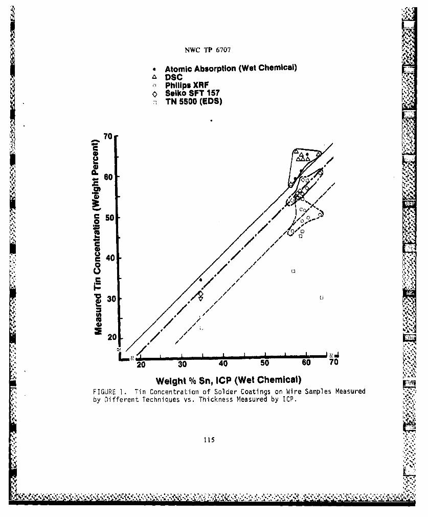
NWC TP 6707
• Atomic Absorption (Wet Chemical)ADSC
Philips XRF< Seiko SFT 157TN 5500 (EDS)
70
*II
C 50
"K 84 / ,",
/ 40-401* ~ 30 :I / ,"/
4) 20 / /
20 30 40 50 60 70
Weight % Sn, ICP (Wet Chemical) ___• FIGURE 1. Tin Concentration of Solder Coatings on Wire Samples Measured
by Different Techniques vs. Thickness Measured by ICP.
11544)•
,•. , 4" 4
* )"

NWC TP 6707
directly measure coating thickness, generally on 2000Xbackscattered electron images.
Coating thickness measurements on the same eightmaterials used in the composition study (Table 1) aregraphed in Figure 2, again using ICP measurements as thestandard of comparison. The Seiko SFT 157 and atomicabsorption measurements are 0.5 to 1.5 =n (20 tO 60 4in)higher. Cross sectional measurements are very scattered,prcbably due to problems with smearing and edge retentionduring mounting and polishing. Improved metallographicprocedures have reduced the scatter since these data werecollected, but cross-section measurement is still consideredless accurate than the other methods.IThe above results show that the Seiko SFT 157 providescoating thickness and composition measurements in'closeagreement with the more time-consuming wet chemical methods.Because of its speed and convenience, the Seiko instrumenthas been chosen for routine characterization of soldercoatings on wire materials.
MICROSTRUCTURE
The microstructure of solder coatings was characterizedusing SEM backscattered electron images, on which lead-richphases appear light and tin-rich phases appear dark. Theaverage size of individual tin-and-lead-rich regions in thesolders was approximated using a lineal intercept procedure,similar to the Heyn method used to determine the grain sizeof materials (Reference 3). The average intercept distancebetween tin-lead phase boundaries is measured by countingthe number of phase boundary intersections on a line ofknown length.
SOLDERABILITY TESTING
Solderability of wire materials and capacitor leads wasmeasured using TM 208 of MIL-STD 202 with variable steam 07Aaging times, and by a wetting balance. The wetting balance 9used is a Multicore Universal Solderability Tester ½.intertaced to a Hewlett Packard 85B computer through an H-P3478A multimeter. The system automatically measures andstores wetting furce approximately 70 times per secondbeginning with electrical corLtact between the wire sampleand the solder bath. The instrument settings used in thisstudy are given below.
Balance Range: 0.75 gImmersion Speed: 20 mm/s
116
Z4

NWC TP 6707
. Atomic Absorption (Wet Chemical)0 Seiko SIT 15746- Cross-Section (SEM)
Solder Thickness, ICP (Mm)0 2 4 6 a 10 1
5 00
1012
;. I,',. 4... .. ,- ,...
400
*1, 300 00
.44
1017
0 100 20030040
Solder Thickness, iCP (Wet Chemical) (XAl n) ::FIGURE 2. Thickness of Solder Coatings Measured by Different w-•Techniques vs. Thickness Measured by ICP. Vertical Lines ConlnectReplicate Cross-Section Measurements on One Material .
117 , ''
"k K
S 4 .I i.;. I - I • • . .I ~ "• * 4 ... - ; • "'-4 l ". i , I

NWC TP 6707Depth: 2.5 mmDuration: 5 sTemperature: 245 deg.CSolder Alloy: 60 Sn-40 PbFlux: Type R (Alpha 100)
After completion of a test, a graph of wetting force vs.time is drawn and parameters, such as time to reach zero Vforce, maximum wetting force (corrected for buoyancy), andtime to reach 0.67 maximum wetting force, are determined andprinted out. Five specimans of each wire sample were F>generally tested to characterize it.
Test method 2022 of MIL-STD 883-C specifies that thetime to reach zero force be less than 0.6 second and that K.the time to reach 0.67 maximum force be less than 1 second.Nearly all of the samples tested satisfy the zero force time h•-
requirement. A much smaller faction satisfied the 0.67maximum force requirement. The time to reach 0.67 maximumwetting force was found to be the wetting-balance parametermost sensitive to differences in wire materials and is usedas the principal solderability parameter in this paper.
The effects of core-metal composition and soldercomposition, thickness, and microstructure on solderabilitywere examined for incoming wires. Samples of various wireswere also studied after exposure to burn-in test thermalcycles (85 deg.C for 40 hours for tantalum capacitors, 125deg.C for 100 hours for ceramic and film capacitors) whichproduce an intermetallic layer at the solder-core interface,and after steam aging at approximately 100 deg.C, 100%relative humidity for various times.
SOLDER COATING PROPERTIES
Within the range of coating thickness examined (7.1 to10.9 iim (280 to 430 4in.)) no effect of thickness onsolderability was found. Solder composition, which variedfrom 30 to 64% tin, also did not show a systematic effect onsolderability. Major differences in solderability, however,were seen for solders having different microstructures. Twogeneral types of electroplated solder coatings were found:fine structured solders (mean intercept distance :0.5=u• (204in.)) plated on some wires by GTE Products Corporation andcoarse-structured solders (mean intercept distance of 3 to4.5 Ium (120 to 175 4in.)) found on all other electroplatedwires. Examples of these coatings for 60 Sn-40 Pb and 30Sn-70 Pb solders are illustrated in Figure 3. Wires withfine-grained coatings exhibit very rapid wetting (t0.67MF
118
Q %k:Z

NWC TrP 6707 .
I INL-GRAINLD COARSE-GRAINED
00-40on NI60-40 an Cu
30-70 onl CCS 30-70 on COS
99FIGURE 3 ,IBackscattered Electron Imiagjes of Polished Cross Sectionsof Solder-Coated WNires. Lead-Rich Phase Appears Light, Tin-Rich
Phadse Dark
119

NWC TP 6707
50.5 sec) as illustrated in the wetting curves shown inFigure 4. The wetting curves for these wires are notsignificantly changed by burn-in testing or steam aging upto 24 hours. Some of the fine-grained solder-coated wiresshow a decrease in wetting force after achieving a maximumvalue, as seen in the copper-clad steel specimen in Figure4. The cause of this and its effect on solder-joint qualityare not known. Complete solder coverage is always seenafter hot dipping on these wires, with no visible dewetting.
Wires coated with coarse-grained solder generallyrequire longer times to reach 0.67 maximum %,etting force.Steam aging increases this wetting time fur.qer for mostcoarse-grained solder-coated wires. Examples of wettingcurves for a coarse-grained, solder-coated wire before andafter steam aging are shown in Figure 5. The dependence ofwetting time before and after steam aging on the coarsenessof the solder coating is shown in Figure 6. The variabilityin wetting times seen for as-received, coarse-grainedsolder-coated wires may be due in part to a variable storagetime after plating before the wire was tested. After 24hours of steam aging, nearly all of the wire coated withcoarse-grained solders require more than 2 seconds to reach0.67 maximum wetting force. The change in wetting time withsteam aging duration is shown in more detail in Figures 7and 8. Most of the increase in wetting times for wires withcoarse-structured coatings is seen to occur in the first 8hours of steam aging.
Reflowed solder coatings have been produced on nickelwire by GTE Products Corporation. For wire originallycoated with fine-grained solder, a coarsening of the soldermicrostructure occurs during reflow (mean intercept distance2 to 3 = after reflow). The thickness of the soldercoating after reflow is specified by GTE to be 1.5 to 12.7urn (60 to 500 4 in.); samples tested in this study generallyhad coating thicknesses from 5 to 10 =m (200 to 400 4 in.).The time to reach 0.67 maximum wetting force is slightlygreater than the original plated wire. As is the case forthe original fine-grained, electroplated wire, no increasein wetting time is seen with steam aging for these wires
(Figure 8).
Wire dipped in molten 60 tin - 40 lead solder afterburn-in was of intermediate grain size (Figure 9) and had acoating thickness ranging from 1.5 to 6.3 rn (60 to 250 w.in.). Significant thickness variation was seen atdifferent regions of a given sample. The time to reach 0.67maximum wetting force varied from 0.5 to 1.9 seconds shortlyafter dipping and increased to 2 to 2.5 seconds after 24
120
%' .'.°

NWC TP 6707 5%
S60-40 on CCS
I d 1 .5112
Zero-4orce time' .27 zt67% of Fmax time! .38 z•*Max. Force! 86 mN
% of Fhx , ti•m2 %
z 80-40 on NI
e
E force time: 27 s 771167%: rax time; .41 s
Ma>.. Force, 77 m'% theoretical, 83 %
FIGURE 4. Typical Wetting Curves of GTE ProductsCorporation Wires Coated with Fine-Structured Solder
121
9
121
S. .
SI•,',, , . J .. •. • • ".• .. " , ,". • . . •'. .: ••i•.". .'• . -' . .".". . •".'..'•'.... ' ' . " ' ''" .

NWC TP 6707 ,, .
a As-recleved
2erofor(-time! 7 1 Z"
Ni
7%' of Fmax time;' ,1 2. 5Mo x, Force: .5,7 mN
% of Fth~eor 7:
t C Steam-aged 24 hra o "C")
122.;'
lL di\I=,s ,
Z2ero-force time, .3,4 ,...67 of Fm•>,x time .:'e'• S' .. ,
Max. Force• .57' mN ••,, o4 Fthec r: 73• ..
FIGURE 5. Typical Wetting Curves for Wires Coated ••
With Coarse-Structured Solder (60 Sn-40 Pb on CCS)...
122 :,-!
I[ ,.-,

NWC TP 6707
0 Reflowed Nlas-recelved
* Reflowed NI, steam-aged 24 hrs.o Cu or CCS, as-recelved* C u or CCS, steam-aged 24 hrs.a NI or NCC, as-recleved
NI or NCC, steam-aged 24 hr..SRedipped Cu or CCS£ Redipped Cu or CCS, ateam-aged 24 hr..S• Redipped NCC
3.5 v Redipped NCC, steam-aged 24 hrs.
S3.0,
0 U..
C V
7 T
) II I. "
'.4 ~ 2.0 I I
.4.
0 o 2 3 4 5
Mean Intercept Distance (Qrn)FIGURE 6. Wetting of 60 Sn 40 Pb Solder-Coated WiresBefore and After Steamn Aging vs. Coarseness of SolderCoatings.
123 ''"

NWC TP 6707
3.5
•,3.0
T T Coarse-grained- -- -- -- 3 on CCS 60/40~2.5 0
aL //0C/
SHot dipped 60/40 on CCS
-1,'. - .- m -/
34.0
E Coarse-grainod2 60/40 on CCS
"0.5
Fino-grainod 80/40 on CCS •••
p p , I I "
5 10 15 20 25Steam Aging Duration (Hours)
FIGURE 7. Effect of Steam Aging Duration on Wetting Time ofSolder Coated Copper-Clad Steel Wires.
124
'xc...'. * .*.* i**~".... *.x

NWC TP 67073.5- • I
'• ,-,.3.0 I
L•_,,I
IL 1 "21: i',i•
"• Hot-dipped 60/40 on Ni " .•i•
z° /'i '/" r:+
' :EI.S ,/
•1.0
.• _1" Reflowed fine-grained 60/40 on Ni .•__
I"0.5 L i ,'r•'-- I"" %`
SFine-grained 60/40 on NCC or Ni•,;!":1•"
E+'+•_
% i% 'oI
• •m i,
0 5 10 15 20 25Steam Aging Duration (Hours) i
,,•,, FIGURE 8, Effect of Steam Aging Duration on ',.letting Time of Solder,, Coated Nickel and Nickel-Clad Wires." i
;I1I
125 ,•;I
la,, o
I I' " I I I i I I I I I I ! i

NWC TP 6707
hours steam aging (Figures 7 and 8). Examples of wettingcurves on hot-dipped wire samples before and after steamaging are shown in Figure 10. The superior performanceclaimed for hot dipped coatings (References 4 and 5) were,thus, not found in this study. The thinner coatingsproduced by hot-dipping may be responsible for theirrelatively slow wetting after steam aging.
0on NI
k'..
FIGURE 9. Backscattered Electron Image of PolishedCross-Section of Wire Dipped in Molten 60 Sn-40 PbSolder
All wire samples examined had at least 95% coverageafter immersion in 60 tin-40 lead solder at 245 deg.C for 5seconds, even after 24 hours steam aging.
V-i-
CORE COMPOSITION AND INTERMETALLIC COMPOUND GROWTH
No differences in solderability of copper and nickelwire coated with equivalent solder coatings was detectable.Burn-in testing at 85 deg.C for 40 hours does not
126

NWC TP 6707
As hot-dipped
V d i =& 5
Zero-force time: ,24 z67% of Fmax time: .38z
.Mx, P'orceL .66 mN% of Ftheor, so %
Steam aged 24 hre
II
•- ,
I d i v'= 51'.
Zero,-f,:rre time: ,.3,2 •
67 of Fm,:, tm irm e 3 :,9 z *,"
Ma*x. Force: 9 m* N, of Ftheor: E:4 %,
FIGURE 10. Typical Wetting Curves for Lead WireHot Dipped in Molten 60 Sn-40 Pb Solder (CCS)
127

NWC TP 6707
significantly change the wetting characteristics of any ofthe wires. Burn-in testing at 125 deg.C for 100 hours,which produces a 1 wm (40 u in.) thick intermetalliccompound layer in nickel wire and a 2 um (80 4 in.)intermetallic layer in copper wire, results in a moderatedecrease in wetting speed for some wires and has no effecton others. Effects of burn-in appear to be similar forcopper and nickel core wires and are generally less severethan the effects of steam aging. This implies that theincrease in wetting times seen with elevated temperatureexposure is due primarily to oxidation rather than growth ofintermetallic compounds. The plating method used by GTE tomanufacture fine-structured solders apparently produces acoating less permeable to oxygen than plating methods usedin the manufacture of coarse-structured coatings.
CAPACITOR FABRICATION
Lead wires on Kemet tantalum and film capacitors areattached using near-eutectic solders at about 200 deg.C.These processes do not have any detectable effects on thesolder coatings of the lead wires in regions where they aresoldered to circuit boards (25mm (0.2 in) from the capacitorcase). Lead wires on hermetically sealed (canned) tantalumand film capacitors have wetting characteristics identicalto the original wire materials. Molded parts are"deflashed" by an abrasive process after molding, whichremoves some of the solder coating near the case. Thiscauses some decrease in wetting speed of the leads. Wireswith fine-grained solder coatings retain a significantadvantage in wetting speed over wires with coarse-grainedcoatings on molded parts, however, and still generally reach0.67 maximum wetting force in less than 1 second.
Ceramic capacitors are required to survive soldering attemperatures up to 250 deg.C, so high melting point soldersare used for lead attachment. These lead-attach processescause some melting of the solder coatings on the lead wires,modifying their thickness and microstructure. The effect ofthis on lead-wire solderability is under investigation.
CONCLUSIONS
1. The wetting speed of solder-coated wire is correlatedwith the microstructure of the solder coating. Wirescoated with coarse-grained solders wet relativelyslowly and are degraded by steam aging. Wires coatedwith fine-grained solders wet very rapidly and areunaffected by steam aging.
128
x"f A ~ \ V ;

NJNWC TP 6707
2. For wires with coarse-grained and hot dipped soldercoatings, time to reach 0.67 maximum wetting forceincreases with steam aging duration up to about 8hours; after 8 hours, little change is seen withadditional steam aging.
3. Hermetically-sealed tantalum capacitors made using wirecoated with fine-grained, electroplated solder, orreflowed, fine-grained solder have lead wires whichexhibit wetting characteristics superior to those ofleads hot-dipped after fabrication, particularly aftersteam aging.
REFERENCES
1. R. L. Fryans, "Determination of the Phase Behavior ofAlloys by Differential Scanning Colorimetry", PerkinElmer Instrument News, Volume 21, No. 1, 1975.
2. D. A. Stout and B. M. Lacy, "The Characterization ofComposite Copper, Nickel and Solder Coatings on SteelWires by Scanning Auger Analysis", Thin Solid Films,Volume 95, 1982, pp. 167-173.
3. ASTM 112-82, "Standard Methods for Determining AverageGrain Size", 1985 Annual Book of Standards, AmericanSociety for Testing and Materials, Philadelphia.
4. Paul E. Davis, Malcom E. Warwick, and Stephen J.Muckett, "Intermetallic Compound Growth andSolderability of Reflowed Tin and Tin-Lead Coatings",Plating and Surface Finishing, Volume 70, 1983, pp.49-53.
5. Roger Wild, "A Review of Component Lead SolderabilityIssues II", Soldering Technology, 9th Annual SeminarProceedings, 1985, p. 49.
2 *"
129 '"'

NWC TP 6707
Alan Geiger is Manager of Materials Technology atUnion Carbide Corp. He has been in Metallurgy for 12years, Ceramics for almost 2 years, and in Solid StatePhysics for 6 years. He received a PhD. in Physics fromCase Western Reserve University in 1969 and is amember of the American Society for Metals and theAmerican Chemical Society.
Address; Union Carbide Corp.Components Dept,P.O, Box 5928Greenville, SC 29606
130
p w
V' 130:

NWC TP 6707
SOLDERABILITY DEFECT ANALYSIS
-SIMPLIFIED
by
John A. DeVoreGeneral Electric CompanyElectronics Laboratory
Syracuse, New York
November 1985
131
NWC TP 6707
ABSTRACT
In 1982, a failure analysis technique known as solderability defect
analysis was formalized and published. The technique was fairlycomplex and required a number of analytical steps to complete. Thepurpose was to define exactly the cause of poor solderability on acomponent part or printed wiring board. This information could then beused to correct the problem through rework or to provide information tovendors to help them correct their processes.
In the past three years an effort has been made to simplify the tech-nique in order to promote a more widespread use. We are now able toprovide an adequate answer within one-half hour of receipt of thesamples.
The simplification process has been achieved through the use of thewetting balance solderability test. It has been found that test curvefine structure will provide a generic answer to the cause of poorsolderability. When this is coupled with the information from thescanning electron microscope/electron microprobe analysis, an exactcause can be determined.
This paper describes the details of the technique, the samples requiredand the basic important details of the wetting balance curves needed tomake determinations. Also included will be a number of case historieswhich show practical use of the technique.
132

NWC TP 6707
Introduction
Approximately two years ago, a method was developedl which we called"Solderability Defect Analysis." The purpose was to provide accurateinformation on the cause of poor solderability of a particular compo-nent lead. This information could then be used to inform the componentvendor where the problem had occurred in his process. The success ofthe method was dependent upon good SEM and chemical analysis informa-tion. This did not detract from the usefulness of the method but didlimit the ability to use it frequently. This was due to the limitedavailability of equipment and the cost associated with it.
Since 1982, we have continually worked to upgrade solderability defectanalysis techniques. These efforts were mainly directed at reducingthe time and cost of analysis, as well as improving its accuracy. Theremainder of this paper describes our latest techniques. Case histo-ries are shown to illustrate technique application.
Basic Technique
The technique of solderability defect analysis is now based on the use
of the wetting balance. In our work to fully identify the mechanismsof solderabillty2 , it was found tht the fine structure in the resultantwetting balance curve gave extremely useful information as to thenature of a solderability problem. Correlating what we saw in thewetting balance with the physical evidence obtained using scanningelectron microscope/electron microprobe techniques, it was foundpossible to fairly accurately define the cause of poor solderbility.
Interpretation of wetting balance curves can give the following Infor-mation.
1) The mechanism of solderability operating.
2) The depth at which a defect resides.
3) The general nature of the defect.
In many cases, this is sufficient information to get a vendor back ontrack to providing parts with good solderability. The technique hasbeen applied to both component leads and larger but fully wettableterminations.
The data from the wetting balance can then be supplemented with bothoptical inspection and SEM/EMA analysis if the equipment is available.
133
0. A
.+ t'..,

NWC TP 6707
Interpretation of Wetting Balance Curves
Since the technique of solderability defect analysis is reliant onwetting balance curves, the generation and interpretation of them isall important.
The basic factor in the generation of the curve is the ability todetect fine structure. Therefore, the physical size of the curvegenerated must be large enough to read. The vertical sensitivity mustbe high enough to detect differences of 2-3 dynes (Nm). The horizontalscale must be such that a 10 sec test time is stretched to 4-5 inches.If a chart recorder is used, then the sensitivity should be 50 mv/secor better and the chart drive (or pen drive) should be 15-20 inches/minor faster. If a computer is used, the important factor is samplingrate. The sample rate should be at least 30 times/sec.
Once the curve is generated, the next step is interpretation. The
following is a list of important indications to look for in a curve.
1) Wetting time (time for the curve to cross the zero axis).
2) Wetting rate.
3) Changes in wetting rate and where they occur.
4) Wetting force at 1 and 2 seconds, at equilibrium, and attest completion.
5) Lack of smoothness in the curve and where it occurs.
6) Withdrawal force.
7) Solderability number 3 .
8) Identification of artifacts in the curve.
For good solderability, wetting times should be short; characteristi-cally, well under 1 second. Longer wetting times indicate a non-reducible film has been encountered. Typically, this is usually anoxide or a stable organic film.
The wetting rate is the indicator of how rapidly the metallurgicalreaction at the surface is taking place. This should be very rapid forgood solderability; characteristically, it should be 300 dynes/sec orfaster. Slow wetting rates indicate a fairly stable oxide is beingreduced or removed slowly.
Changes in wetting rate are a very important indicator. By use of thisinformation, a defects location may be determined. Typically, one
134 ... -
.4ta

NWC TP 6707 I
notices this effect on plated parts. The most common effect is to seea very fast initial wetting rate which suddenly changes to a slowerwetting rate. This shows that the surface plating is very wettable or•-
alloyable. Once the solder reaches the interface between the surfaceplate and the metal underneath, the wptting rate of that surface willbe seen. If it is "clean", no change in rate will be noted. However,if it is "dirty", the wetting rate will slow down. This usually indi-cates poor cleaning prior to final plating. By noting the time betweeninitial wetting and the change in rate, the location of the defect canbe estimated.
Wetting force evaluation is the next important indicator. The wettingforce is an indicator of the quality of metallurgical wetting. Com-plete and uniform wetting will give high wetting forces; usually over,.1275 dynes/cm. Less then this will indicate incomplete or non-uniformwetting. Since most of our production soldering processes are operatedon the basis of 1-5 seconds contact time with the molten solder, it isimportant that maximum wetting takes place in this time. Based onthis, we prefer to see nearly maximum wetting in 2 seconds or less.Therefore, we like to see the wetting force above 250 d~ynes/cm at 2seconds. Less than this indicates non-reducible materials at thesolder bond which could affect joint strength or life (i.e., fatigue).Lack of smoothness in the curve most often indicates gas evolution. As
the bubbles of gas are released and interface with the meniscus, thewetting force goes up and down. Since the evolution of gas is part ofthe dewetting mechanism, this is an important factor to note. Itshould be said that not all gases cause dewetting but they can intro-duce voids into a solder joint. The lack of smoothness in the curve Ismrost often noted at the knee.
The most reliable indicator of dewetting we have found to date is thewithdrawal force. This force is measured from the maximum wettingforce. Typically, we like to see this force less than 100 dynes/cm.Greater than this indicates significant dewetting has occurred. Typi-cal defects causing dewetting are organics in plated coatings• andwater of hydration in inorganics (i.e., hydrated oxide). Many timesthe gas evolution indicators and the dewetting indicator can be cor-related to estimate defect location. This is not quantitative andtakes some experience.
Effects of artifacts on the curve must be subtracted during the curveevaluation. Artifacts can come from obvious sources such as impacts orexcessive vibration during test, poor recording equipment or testermalfunction. One artifact often not recognized as such is a drop inthe curve after the knee. This, in reality, is most often a fluxfunction not related to the sample under test. Since all testing forsolderability defect analysis should be done with type "R" flux, thedrop most often occurs when too much flux is used. Physically, what
135
I

NWC TP 6707
happens is that the excess flux runs away from the area of the sample.This draws much of the flux away from the area of the meniscus allowingsurface tension to rise and wetting force to drop. When such a drop isnoted, always look at the surface of the solder pot near the sample.To prevent this problem from occurring, always use a thin film of fluxand make sure that there is not a droplet of flux on the end of thelead.
Supplementary Techniques
The major supplementary technique is solderability defect analysis isscanning electron microscopy and electron microprobe analyses (SEM/EMA). The details of this technique may be found in my previouspaper'. The major advantge of using SEM/EMA is to more accuratelydefine the cause of the defect.
Optical microscopy is also useful and generally available to everyone.Both the low power stereo microscopes and the higher power metallurgi-cal microscopes fall into this category. As a minimum, the samplewhich had been wetting balance tested should always be examined with astereo microscope. Much useful information can be collected this way.An excellent example is shown in the case histories.
Relations with Vendors
The rules in dealing with vendors are fairly simple but quite rigid.
The first rule is to deal on the technical level only. This requiresgetting past the purchasing/marketing organizations. The second ruleis having hard technical data in your hand. This what "SolderbilityDefect..Analysis" is all about. The third rule is to inspire coopera- o:tion rather than conflict. Obeying rule two goes a long way towardthis objective. As a corollary, it should be instilled that it is toboth parties benefit to solve the problem.
Case Histories
I.Transistor Leads ,
The leads on transistors from this vendor had a history of poor
solderability as evidenced by a high solder joint touchup rate.The leads are tin plate over alloy 42. Figure 1 shows the wettingbalance trace. The major features seen in the curve are a changeof wetting rate and a high withdrawal force. The analysis of wet-ting rate shows that the tin plate wet very fast. As soon as itwas alloyed off, wetting rate slowed down dramatically indicatingthe problem was at the tin plate/base metal interface. The high
136
%. 1

NWC TP 6707
Figure 1
withdrawal force showed dewetting to be the problem. In otherwords, dirty base metal prior to plating. Discussions with thevendor located the exact problem. The lead frame is processed inmachinery using a die lubricant of silicones.
2. Copper Lugs
Tin plated copper lugs from one vendor were found to be hard tosolder. When soldered, the Joints had very low strength. Figure 2 ''Mshows the wetting balance trace.
, -o 1ý ,
'.4,
Figure 2137
.4 :. ~ ~ ." . . C •=

NWC TP 6707
The curve shows slow wetting (5.2 seconds), wetting rate change,low wetting force and high withdrawal force. The analysis of thecurve indicated a non-wetable material at the tin plate/base metalinterface. This same material caused significant dewetting.SEM/EMA analysis located the exact problem. Figure 3 shows thesolderability tested surface. Microprobe analysis showed the"rocks" were aluminum oxide and were embedded in the copper. Theconclusion was that tumbling media used for deburring of thestamped tabs was being embedded and not removed prior to plating.
Figure 3
3. IC Flatpack .
The leads of a flatpack package were to be evaluated for soldera-bility. These were gold plated over 42 alloy base metal. Figure 4shows the wetting balance trace taken. The main feature is thatthe trace never rose above the zero axis when tested for 5 seconds-
.,P
This indicated something on the surface of the gold plate was non-A I.
wettable. SEM examination showed a very stable organic on thesurface. This was in two forms as shown in Figure 5. The worst
was the heavy deposit which caused non-wetting. The second wasmore stain-like which caused dewetting. Optical examination of the
solderability tested samples showed the spots were in distinct
lines across the leads. This can be seen in Figure 6. The conclu-sion was contaminated test fixtures used by the package manufac-turer.
138
V' .• -. ' ' -' ' '''''., .,- -:•. \ .,•, \.,.,'-'v )'.,,,•,.,,•• - -• .,.,...,.,.,.,,•,-• ''. ,.-.
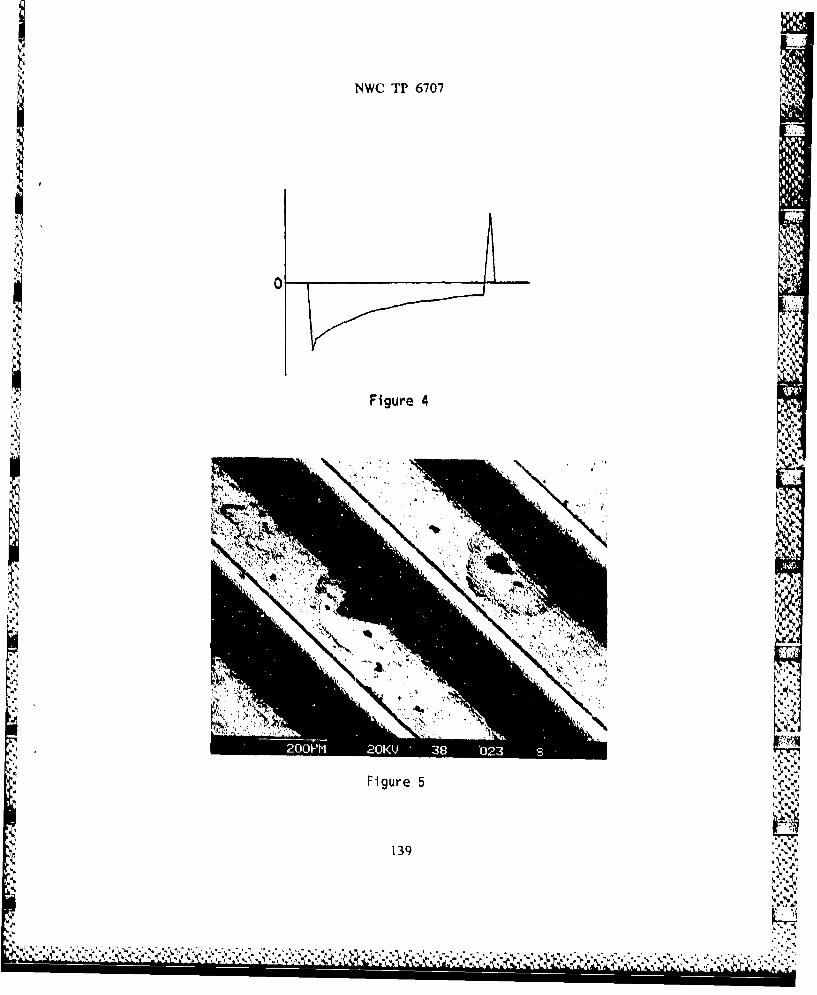
NWC TP 6707
A"A
Figure 5
139

ipNWC TP 6707/
Figure 6
Summary
1. "Solderability Defect Analysis" is a very useful technique insolving problems of solderability "up front."
2. Through the use of the wetting balance, the technique is availableto both users and vendors. It can be performed on a routine basisat low cost.
3. The technique can now be used to identify the generic nature of adefect causing bad solderability very rapidly (often in less thanone-half hour).
4. For complete identification of a defect, it is necessary to use thesupplementary analysis techniques of SEM/EMA, cross-section andoptical microscopy.
4"1.
References
1. "Solderability Defect Analysis," J. A. DeVore, Sixth AnnualSoldering Technology Seminar, China Lake CA. February 1987.
2. "The Mechanisms of Solderability and Solderability-RelatedFailures," J. A. DeVore, Proceedings of Printed Circuit WorldConvention III, May 1984.
"140
m.p.

NWC TP 6707
3. "Solderability," J. A. DeVore, Journal of Metals, July 1984.
4. "Co-Deposited Organics in Plated Coatings - A Problem," J. A.DeVore, Fifth Annual Soldering Technology Seminar, China Lake CA,February 198I.
ýp.
.fll
141
41
vI C,

NWC TP 6707
John DeVore, Senior Metallurgist with the ReliabilityEngineering Subsection of the Electronics Laboratory atthe General Electric Co., received his BS degree inMetallurgical Engineering from the Michigan College ofMining and Technology in 1959. An active member of theAmerican Society for Metals, John was also elected tomembership in Alpha Sigma Mu, the national honoraryfraternity. A significant portion of his time is spentworking in the area of soldering and solderability, hismost recent work being in the refinement of wettingbalance solderability testing, He is co-author of the firstSolder and Solder Joint Properties Handbook, and isactive in the development of government, national, andinternational standardization in soldering and printedwiring boards,
Address: General Electric Co.3-21 Electronics ParkSyracuse, NY 13221
142
NWC TP 6707
SOLDER DEFECT MODE ANALYSIS UNDER THE"ZERO" DEFECT CONCEPT
byF. Zado
AT&T Technologies
For a copy of this paper, please contact
Frank ZadoAT&T TechnologiesP. O. Box 900Princeton, NJ 08440
143
NWC PP 6707
DYNAMIC MECHANICAL TESTING OF SOLDERAND SOLDER JOINTS
by
Linda D. LauerMartin Marietta Orlando Aerospace
Orlando, Florida
ABSTRACT
Successful use of solder joints to attach surface mounted
devices to printed wiring board substrates requires knowledge of thestress-strain properties of solder as function, of temperature, time,and loading conditions. in addition, the relatively high operatingtemperature of solder in comparison to its absolute melting tempera-
ture introduces a requirement for an understanding of the influenceof creep effects on the mechanical properties of solder under cycli-cal loading conditions. In the past, studies of these solder proper-ties have been limited by the need to use relatively large bulksolder samples that may or may not be representative of actual solderjoints in a printed wiring board-chip carrier environment.
A previously unreported test method for the evaluation of thedynamic mechanical properties of solder and solder joints has beendeveloped. The method is uased upon the use of a Rheometrics Dynamic
Spectrometer, which has been shown to be capable of determining boththe elastic and plastic responses of solder joints during cyclicalloading under a variety of imposed strains, strain rates, and temper-atures that are within the range of anticipated service conditions.In addition, stress relaxation properties of solder joints may bestudied.
INTRODUCTION
Solder joint reliability continues to be one of the most criti-cal technical issues in surface mount technology development, sincethe solder joint serves as both the mechanical and the electricallink between the component and the printed wiring board. Although avariety of factors may cause solder joint failures, it is generallyrecognized that the primary source of failure is low cycle-strain-controlled fatigue that arises when the assembly is subjected totemperature variations (References 1-6). Such conditions as ambienttemperature changes, power dissipation in chip carriers, and poweron/off will, when combined with the unequal thermal properties of thecomponent and the printed wiring board materiais, result in stressesand strains that can ultimately result in solder joint failure.Q 1985 Martin Marietta Corporation. Reprinted by permission.
PREVIOUS PAGR
145
*j.q.*.. ... , , . . .. . .. . .. . ... . . . . . .. . , . . . . . . '.. *2..y

NWC TP 6707
Cyclic fatigue damage in solder joints has been related to creepor stress relaxation effects that occur when solder is subjected to astrain at normal service conditions (Reference 7). The presence ofsignificant creep effects is, in turn, due to the relatively highservice temperature of solder in comparison to its reflow tempera-ture. The amount of damage that occurs in a given cycle is bothtime- and temperature-dependent. These characteristics can havesignificant consequences for any attempt to design eithcr an analyti-cal or an experime,'tal progrew. to investigate solder joint reliabil-ity. It is thereforu necessary to address both the elastic and theinelastic (creep or stress relaxation) responses of solder in orderto fully understand Uie mechanical behavior of solder joints undercyclical loading !rcoditions.
EXPERIMENTAL
DYNAMIC MECHANICAL ANALYSIS OVERVIEW
Dynamic mechanical analysis is a technique that may be used tomeasure the ability of a material to store and dissipate (throughrelaxation processes) mechanical energy. When a material such assolder is subjected to a sinusoidally varying strain, the resultantstress will also change in a sinusoidal manner. However, the stresswill not be in phase with the strain due to the presence of stressrelaxation processes in the solder, but instead is shifted in phase Oby an angle 8 . This is illustrated in Figure 1A. The stressresponse can be mathematically described as the combination of twoseparate sinusoidal waves, one of which is in phase with the strain,and the other of which is exactly ninety degrees out of phase with
the strain. The relative amplitudes of these two waves are dependentupon the value of S. This is illustrated in Figure 1B. It can beshown, through arguments too complex to discuss in this brief over-view, that the amplitude of the in-phase component of the stressresponse is related to the amount of energy that is stored elastical-ly in the sample, and that the amplitude of the 90 degree out-of-
phase component of the stress response is related to the amount ofenergy that is lost through an inelastic or plastic response, such as .creep or stress relaxation (Reference 8).
Figure 2 shows a block diagram of a Rheometrics Dynamic Spectro-meter (RDS-7700, manufactured by Rheometrics, Inc., Piscataway,N.J.), which is designed for dynamic mechanical testing of a widerange of materials. This diagram shows the signal flow and intercon-nection of major components. In operating the system, the user firstclamps the sample between two fixtures, one of which is driven by amotor, and the other of which is rigidly mounted to a transducer.The user then selects the deformation that is to be applied to thesample by specifying both the strain and the strain rate (or sinu-
soidaL test frequency) that is to be used. Samples may I <
146

NWC TP 6707
%
I I Strain
/ strestI I
Figure IA. The strain and resultant stress for a viscoelasticmaterial are offset during dynamic mechanical testing.
Time 10
Stress In Phase
with Strain
_%/ % Stress ResponseS % % "%• S/ tress ,O'
I Out of PhaseI Iwith Strain:•\ ! /u \ \ I,
.0//
Figure 1B. The stress response in Figure 1A can be mathematicallydescribed as the sum of two stress components: one In phase withthe strain, and the other 900 out of phase with the strain.
147
*. ,.K~* ~ I

NWC TP 6707
X.2CLC
ý4puewujU
0 uiejs CL -
*r=
c o 0
4a)
o 00
0
cn oo
- ~0)
m) 4)
Z,. 0 > 0OU7U'n m 0
0H

NWC TP 6707be tested in shear or tension-compression. Alternatively, stepstrains may be applied for direct stress relaxation studies. Aprecision motor controlled by a position servomechanism applies a
deformation to the material, with the frequency and amplitude of thedeformation controlled by the central processor. The actual strainis measured using a position transducer that is coupled directly to
the motor shaft. This eliminates possible errors due to servodynamics.
The torque and the normal force that are generated in response
to this imposed motion are measured by the transducer. For the work
reported in this paper, a temperature-controlled transducer with a
maximum normal force load of 2000 grams was used. The deformation ,
force signals, plus the strain signal, are amplified and input to thecentral processor. The central processor contains a sampling sine
wave correlator which rejects both harmonics and noise, and calcu-
lates the values of the elastic and inelastic components of thedeformation process based upon the peak magnitude of the force and
the phase angle shift between the stress and the strain. The temper-
ature Is controlled throughout the test using convected gas in an
environmental chamber that surrounds the sample.
BULK SOLDER TESTS
Tests on bulk solder were conducted with 1.1" x 0.2" x 0.065"
cast solder bars. Each solder bar was polished to a 600 grit finish,
with polishing performed in the longitudinal direction to avoid pro-
mature crack nucleation during testing. The solder bars were direct-
ly loaded into the RDS-7700 and were tested in a tension-compression
mode.
SOLDER JOINT TESTS
Several types of fixtures were designed, fabricated, and evalu-
ated for solder joint testing. The final test fixture design isshown in Figure 3. The test fixture, which was fabricated fromstainless steel, is composed fo two identical halves. In use, a
single chip carrier-solder joint-substrate assembly is attachedbetween the two fixture halves by using a rigid epoxy adhesive on the
back of the substrate and on top of the chip carrier. The two fix- 7Z
ture halves, with the solder joint assembly between them, are then
mounted in the tension-compression fixture of the RDS.
The chip carrier-solder joint-substrate sample that is used inthe test procedure is shown in Figure 4. Note than the chip carrier
and the substrate are attached by only two solder joints that aredirectly opposite one another. These solder joints carry the entire
applied load during the test. The imaginary line between the two
149
%U'. '"
NWC TP 6707
X
o0 c
CL
.~E to
.0 0- c
m0p
SE ii0 C
U.
.) 4-4
4--
Ci~ 4-i
0~ 0
I.-.
0V)
0 C0
0 o2
.0
o- m w l
0 U)
0 5

NWC TP 6707
t-,4 i. L* U,
S8 .'.2...
• • ']
0.9•
SI I 'dT0
-QL ,,Ntr -
a 151,'-
p V.. 9,
,d:
"U, , • .,. •" - ,•, . x , , . -• •. ,".,, .", ••.,.,,.. ,• • , • • .% \ ••., ." '. "', ' ."'''," % ,••/ " ",': , .••• • , • t •'"'¢ - •3' J • •

NWC TP 6707 INsolder joints is placed parallel to the direction of movement of thetension-compression fixture during testing. When Loading the testfixture, the torque and normal loads on the transducer are carefullymonitored to ensure that the solder joints are not subjected tostresses prior to test initiation.
RESULTS AND DISCUSSION
DYNAMIC MECHANICAL TESTING OF SOLDER BARS
Figures 5 and 6 show the results of frequency sweeps onSn63-Pb37 and Sn62-Pb36-Ag2 solder bars, resper.LiveLy. In this modeof testing, the frequency of the sinusoidal deformation that isapplied to the solder is varied, while the strain remains constant.Note that this is equivalent to studying the response of solder tovarying strain rates. The tests results that are shown in Figures 5and 6 were obtained at 30 degrees C with a strain of 0.25%.
Examination of the test data shows that the elastic modulus ofsolder, while dependent upon solder composition, is fairly indepen-dent of strain rate at room temperature. The loss modulus, which isa measure of the extent of inelastic or plastic response of thematerial, is, however, dependent upon strain rate. Two distinctmaxima are present in the loss modulus curves. The first of theseoccurs at or below a frequency of 0.01 radians per second (the mini-mum attainable frequency on the RDS), and the second occurs at afrequency between I and 10 radians per second. The higher values ofthe Loss moduli in these two regions are indicative of the presenceof two separate and strain-rate-dependent plastic response mechanismsin solder. This is consistent with slip (at high strain rates) andgrain boundary sliding (at low strain rates) deformation modes.
In comparing the data in Figures 5 and 6, it can be seen that
dynamic mechanical analysis is quite sensitive to changes in solderalloy compositLon. The presence fo 2% silver in a tin-lead alloyresults in a Large increase in the elastic modulus and a dramaticdecrease in the loss modulus of the solder. The Latter observationis particularly interesting, since a decrease in loss modulus is con-sistent with a decreased tendency toward inelastic deformation ofsolder in response to an imposed strain. Cyclic damage accumulationin solders has been related to the amount of grain boundary slidingthat occurs in the alloy structure. The lower loss modulus of the
Sn62-Pb36-Ag2 solder in comparison to the Sn63-Pb37 solder is consis-tent with Less grain boundary sliding, and thus improved fatigueresistance, in the silver-containing alloy. This is consistent withresults of actual thermal fatigue tests on surface-mountedcomponents.
152
.1- ZL

R'.
NWC TP 6707
1.O E 11
Figure 5. Sn 63-Pb37 solder bar
I%
1.0 E 11 Frequency (rad/sec)10 1Figure 6. Sn 62-Pb 36- Ag 2 solder bar
vt
Frequency Sweep at 0.25% Strain E -Elastic ModulusTemperature =30 Deg C E =Lose Modulus
1.0iE 100Frequency (rad/icc)
153
.6.

NWC TP 6707
The stress-strain response of solder bars as a function ofapplied strain at constant test frequency was also measured. Figure7 shows the results of a strain sweep of Sn62-Pb36-Ag2 solder at 100degrees C. The elastic modulus was found to be relatively indepen-dent of the strain. The loss modulus, however, was found to bestrain-dependent under the same test conditions. In general, the
value of the loss modulus was high at Low strain levels, decreased asthe strain was increased, and then began to increase as the strainwas further increased. This behavior is once again consistent withthe presence of two separate deformation mechanisms that are strain-rate dependent. •
Stress relaxation tests wre also performed on solder bars.Figure 8 shows the results for stress relaxation tests for Sn63-Pb37solder at -65 and 100 degrees C, respectively. Two interesting
observations can be made from this data. First, stress relaxation insolder is a very lengthy process. Changes in the relaxation modulus(the ratio of streds to st a.in) were still occurting aftr 1000seconds at both temperatures that were examined. This is consistentwith the fact that the thermal cycling behavior of solder isdependent not only upon the rate and extent of temperature change,but also upon the hold time at the upper and lower temperaturelimits. In addition, it is interesting to note that, although stressrelaxation is much more extensive at elevated temperatures,considerable stress relaxation can occur in solder even at -65degrees C.
Figure 9 shows the effect of solder composition on the stressrelaxation properties of Sn40-Pb60, Sn63-Pb37, and Sn62-Pb36-Ag2solder alloys at 100 degrees C. Note that the two tin-lead soldersare very similar in their stress relaxation behavior. The Sn62-Pb36-Ag2 solder, however, shows relatively little stress relaxation incomparison to the tin-lead solders. This is consistent with thesuperior fatigue resistance properties of the silver-containingalloy.
DYNAMIC MECHANICAL TESTING OF SOLDER JOINTS
During the initial evaluation of the dynamic mechanical proper-ties of solder joints, two types of solder were tested. The firstseries of solder joints were prepared from a standard Sn62-Pb36-Ag2solder paste. The other series of solder joints was also preparedfrom Sn62-Pb36-Ag2 solder. However, the alloy reportedly containedgrain refiners for improved fatigue life.
Dynamic mechanical properties of the two types of solder jointswere first examined by conducting frequency sweeps at 30 degrees Cand strain of 0.5%. Test results for the two solders are compared in'" 01
154
., ,"".
44A

NWC TP 67071.0 EI
I0
E -Elastic ModulusE" Lose Modulus
Figure 7. Sn 62 Pb 36 Ag 2 strain sweep, 0.1 rad/see, 100 deg.
10K %tralnOP0761 -7
w 11001C
1.0 E 90 100 200 300 400 500 600 700 Soo 900 1000
Time (*so)Figure 8. The effect of temperature on the stress relaxation of Sn63-Pb 37 solder bars. Test mode: 0.1% step strain in tension.
155
'y(.: ~. ... ,.. - ~ c~ *.-, .~**v** * N

1.0 ~ ¶0NWC TP 6707
1, F1
100 00 00 40 SO 60 70 *aNo0 1000
0 Time teeC)
Figure 9. The effect Of solder colAPOsitif ntesrs eaaiT
of solder bars-test mode% o.1% step strain in tension at 100*CC
Figue 10. Sn 62 -Pb 36 - g 2 solder Joint
II
s tandard SoWt"f- l3iMdUU
-Loss Modulus
0.01 Frequomoy (rid/seo)
156
.57
*5K

NWC TP 6707Figure 10. Note that in Figure 10, as in other data that was
obtained on solder joints, only relative mudulus values are reported.
This is a result of the fact that, in order to calculate true modulus
values, sample dimensions must be known. In the case of solder bars,the measurements of length, width, and thickness were straight-
forward. The complex shape of a solder joint, however, cannot be
described by only three values. Therefore, a decision was made to
input "ballpark" dimensional values into the RDS computer and to
closely monitor solder joint geometries in order to ensure that valid
comparisons could be made between different experiments. Particular
attention was paid to ensuring that the stand-off height of the comp-
orients was consistent from sample to sample by using small, removable
shims under the component during the soldering process.
Examination of the data in Figure 10 shows that the dynamic
mechanical properties of solder joints formed from the two different
types of Sn62-Pb36-Ag2 solder are very similar at room temperature,with the elastic moduli being almost identical. The loss modulus of
the standard solder is slightly lower that the loss modulus of the
fatigue-resistant solder, particularly at Low strain rates (Low testfrequencies).
The two solders were also compared at -65 and 100 degrees C. At
-65 degrees C, the two solders have identical elastic moduli. The
V, loss moduli for the two solders are below the detection limit of the
RDS. At 100 degrees C, the elastic moduli of the two solders are
again very similar. The loss modulus of the standard solder is some-
what lower than the loss modulus of the fatigue-resistant solder at
low strain rates, with the differences between the two solders
virtually disappearing as the strain rate is increased. This data is
shown in Figure 11.
% Based upon previous arguments, a relatively Low loss modulus
implies that only a small amount of grain boundary sliding occurs
during deformation, and the solder would thus show less cyclicalfatigue resistance than a solder with a higher loss modulus. The
"data in Figures 10 and 11 do not support the claim that the addition
of grain refiners improves the fatigue life of Sn62-Pb36-Ag! solder.
Thermal cycling tests that were conducted on surface-mounted compon-
ents subsequently confirmed thaL there was no significant difference
in the fatigue behavior of the two solders.
Stress relaxation tests were performed on solder joints preparedfrom the standard Sn62-Pb36-Ag2 solder paste. Typical test resultsare shown in Figure 12. Note that the stress relaxation properties
that were observed for solder joints varied from the results that
were obtained for bulk solder bars (shown in Figure 9) in terms of
[ %4
4 A157l'
•, ".,,". ',," ".". .. ", ." .. ," ".". .x, " ,,, ",. • ,.' •Y > '• • '••," "i',"," •.• • b''.'"b"•%' " "' ,,• ,"'•',,,X.",,,'.

NWC TP 67071.0 E 13
Prequency Sweeps at 0.50% StrainTemperature - 100 Degrees C
Iu
" - "O Standard Solder E' .. Elatio ModulusA-4 Grain-Refinod Solder E" - Lose Modulus
100Frequency (red/moO) I
Figure 11. Sn 62 - Pb 36 - Ag 2 solder joint
9.0 E 11-
Figure 12. Stress relaxation of Sn 62 - Pb 36 - Ag 2 solderjoints following a 0.5Z step strain in tension at 1000C.
0 100 200 300 400 500 600 700 800 900 1000Time (sea)IL,*-.
158
• ' , ,, , I II I I2
NWC TP 6707the extent of relaxation that occurred. This may represent theeffect of a compliant resin layer in the printed wiring board sub-strate to which the solder joints were attached. Such a resin layercould contribute to the observed stress relaxation properties of thesolder joint assembly.
The effect of repeated mechanical cycling on the dynamic mechan-S. ical properties of solder joints was investigated at -65, 30, and 100
degrees C. Samples were subjected to sinusoidal oscillations with atest frequency of 0.01 radians per second (approximately 10 minutesper cycle) and a test strain of 0.5%. Dynamic mechanical propertieswere periodically measured during the test.
Initial tests were conducted at 30 dgrees C, with the hopes thatthe mechanical strain induced by the Rheometrics Dynamic Spectometerwould mimic the effects of thermal expansion and contraction of aprinted wiring board substrate on a solder joint. Repeated tests,however, failed to reveal a change in dynamic mechanical propertiesof solder joints as a function of time (or number of cycles). Forexample, a sample that was prepared from standard Sn62-Pb36-Ag2solder showed no significant change in either the elastic modulus orthe loss modulus after 575 cycles. Upon removal from the RDS, bothsolder joints were intact. Examination of the solder surface byscanning electronc microscopy showed that, at a magnification of
500K, small cracks could be seen in the solder surface (Figure 13). V,
However, no evidence of cracks in the solder could be seen in asolder joint cross-section thaL was examined at 100X.
Efforts to conduct time sweeps on solder joints at -65 degrees Cwere complicated by the fact that the loss modulus of solder at thistemperature is too low to be detected. Preliminary tests showed that
after 40 cycles at -65 degrees C, no change in the elastic modulus ofthe solder could be seen. Scanning electronc microscopy examinationof the solder surface revealed the presence of numerous small cracks.Microscopic examination of a cross-section of the joint, however,showed that these cracks did not extend into the solder for an appre- k
ciable distance.
Major changes in the dynamic mechanical properties of solderjoints were seen during time sweeps at 100 degrees C. Figure 14shows the dynamic mechanical property changes that occurred in aSn62-Pb36-Ag2 solder joint sample that was subjected to 50 mechanicalcycles. The elastic modulus of the solder showed a significantdecrease, and the loss modulus showed a significant increase, duringthe test. In spite of these large dynamic mechanical propertychanges, both solder joints were intact upon completion of the test.Scanning electron microscopy examination of the solder joint surfacesand cross-sections at magnifications up to lO0OX showed no evidenceof structural damage to the solder joints.
159
S. *'*- ,, *- . .. . ,..'. .-. .*, .. v .... ',-* ..
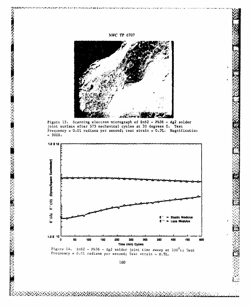
INWC Tr 6707
t f
Figure 13. Scanning electron micrograph of~ Sn62 -Pb36 -A&2 solder
joint surface after 575 mechanical cycles at 30 degrees C. TesLFrequency 0.01. radians per second; test strain 0.5%,. Magnification
500X,
.9 ~~1.0 E 13 A
E ElsticModulus9 Lose Moduluei
aA 50O 100 ISOf 200A 26 10 36 00 4 o
Time (mini) CyclesFigure 14 n2- Pb36 - Ag2 solder joint time sweep at 1000c; Test
Freuecy .0. rdins arsecond; Test strain 0.%
1601

NWC TP 6707Repeated experiments on Sn62-Pb36-Ag2 solder joints showed the
same trend; i.e., at 100 degrees C, repeated mechanical cyclingresults in a large decrease in the elastic modulus and a significant
increase in the loss modulus. However, the rate of increase and
decrease of these properties was found to vary somewhat from sample
to sample. For example, one solder joint sample reached a point
where the elastic modulus was only slightly higher than the loss
modulus after only 11 cycles. Mechanical cycling of the sample was
"stopped at this point, and the solder joints were examined. Both
solder joints were found to be intact.
When mechanical cycling was continued beyond the point when the
elastic and loss moduli became equal in value, or until the loss
modulus had a higher value than the elastic modulus, one or both of
the sample solder joints were found to be broken at the conclusion of
the test. For example, tests on one Sn62-Pb36-Ag2 solder joint
sample showed that the loss modulus and the elastic modulus became
equal in value after only nine cycles. After 15 cycles, when the
test was stopped, the loss modulus had a higher value than the elas-
tic modulus. This data is shown in Figure 15. Both solder joints in
the sample were found to be broken at the conclusion of the test.
Examination of the surface of one of the fractured solder joints
showed numerous voids that may have contributed to premature faLlure
of the sample (Figure 16). At higher magnifications, the solder
.4surface showed a typical topography associated with fatigue failureA(Figure 17). The second solder joint from the sample, while showing
fewer voids than the first solder joint, also showed evidence of
fatigue failure.
CONCLUSIONS
Based upon the results of work that has been conducted to date,it has been shown that dynamic mechanical analysis io a viable method
for invesLigating the mechanical properties of solder and solder
joints under cyclical loading conditions. One major advantage of the
test technique is that both the elastic and inelastic responses ofsolder are simultaneously measured.
Dynamic mechanical analysis has been ahown to he sensitive to
the well-known strain-rate sensitivity of solder. In addition, the
ability of the technique to provide information regarding the stress
relaxation properties of solder has been established. The potential
ability of the technique to assist in the evaluation of the relative
fatigue resistance properties of different solder alloys has beenshown not only by the fact that dynamic mechanical test data were
consistent with known fatigue resistance characteristics of two dif-,
ferent solder alloys, but also by the fact that the technique was
successfuly used to predict that two solders that reportedly differed
in fatigue resistance would in fact perform almost identically.
161I,:'

NWC TP 6707
1.0 E 13
w
E' Elastic ModulusE " - Loss Modulus
1.0 E 100 20 40 60 s0 100 120 140 160 160 200
Time (mrn) Cycles
Figure 15. Dynamic mechanical property changes of 5n62 - Pb36 - Ag 2solder joint sample as a Function of time at 100 0C. Test frequencywas 0.01 radians per second; test strain was 0.5%. Both solder jointswere broken as a result of this test.
*1,
Figure 16. Scanning electron microscope of a Fractured surface of aSn62 - Pb36 - Ag2 solder joint that broke during mechanical testing.Numeroits voids are visible. Magnification 50X.
162

NWC TP 6707
Figure 1.7. Solder joint surface from Figure 16 at a magnification of200X.
163
~ No.

NWC TP 6707
REFERENCES
1. R.N. Wild, "Some Fatigue Properties of Solder and SolderJoints," NEPCON, pp. 105-117 (1974).
2. E. Levine, J. Ordonez, "Analysis of Thermal Cycle Fatigue Damagein Microsocket Solder Joints," IEEE Tr. Camp., Hybrids, Mfg.Tech., Vol. CHMT-4(4), pp. 515-519, Dec. 1981.
3. J.T. Lynch, M.R. Ford, A. Boetti, "The Effect of HighDissipation Components on the Solder Joints of Ceramic ChipCarriers Attached to Thick Film Alumina Substrates," IEEE Tr.Comp., Hybrids, Mfg. Tech., Vol. CHMT-6(3), pp. 237-245, Sep.1983.
4. D.L. Walker. L.R. Fox, R.J. Hannemann, "Analysis of SurfaceMount Thermal and Thermal Stress Performance," IEEE Tr. Comp.,Hybrids, Mfg. Tech., Vol. CHMT-6(3), Sep. 1983.
5. J.F. Burgess, R.O. Carlson, H.H. Glascock, C.A. Neugebauer, H.F.Webster, "Solder Fatigue Problems in Power Packages," IEEE Proc.34th Elec. Comp. Conf,, pp. 144-148 (1984).
6. J.M. Smeby, "Solder Joint Behavior in HCC/PWB Interconnects,"IIEEE Proc. 34th Elec. Comp. Conf., pp. 117-124 (1984).
7. W. Engelmair, "Functional Cycling and Surface MountingAttachment Reliability," Surface Mount Technology, Tech.Monograph Series 6984-02, ISHM, Silver Springs, Maryland, 1984.
8. J.D. Ferry, "Viscoelastic Properties of Polymers," 3rd Ed., JohnWiley & Sons, Inc., New York, NY, 1980.
I
164
I,4 'A
NWC TP 6707
Linda Lauer has a Ph.D in Inorganic Chemistry fromDuquesne University (1975) and was a chemistryinstructor at the U.S. Naval Academy before joiningMartin Marietta in 1980. As a Staff Engineer with theOrlando Aerospace group, she is responsible for processsupport and advanced material testing in the areas ofprinted wiring board and structural composite resinsystems. Linda is also involved in applications ofdynamic mechanical testing in the study of non-resin
systems, including solder. She is a member of theAmerican Chemical Society and is past Senior NationalDirector for the Central Florida Chapter of the Societyfor the Advancement of Material and ProcessEngineering.
Address: Martin Marietta AerospaceP.O. Box 5837, MP 88Orlando, FL 32855
IIV165 ~
V??

NWC TP 6707
1>, STATISTICS, DESIGNED EXPERIMENTS, ANDPRINTED WIRING BOARD ASSEMBLY
I byLarry R. Lichtenberg, Meridith Sleiman, and Mikel J. Harry, Ph.D.
Motorola Inc. Government Electronics Group,Scottsdale, Arizona
ABSTRACT
During the past few years, statistical process control and experiment design concepts have ,,i• ~~taken a prominent place within the industry. The use of such tools within the Motorola, GEG ;',
manufacturing environment, has grown to the point where reflow and wave solder process devel-opment and optimization has significantly benefited.
The ability to statistically evaluate and model various known and unknown phenomena, hasprovided GEG's manufacturing technology with a series of very powerful tools to aid in processcontrol and development. The primary purpose of this paper is to present the various approachesused by GEG to implement the previously mentioned statistical tools, with respect to the devel-opment of infrared (IR) reflow solder processes and enhancement of certain quality characteris-tics associated with wave soldered printed wiring boards (PWB's). Beyond specific GEGapplications, the paper discuses the role of statistically designed experiments and process controlmethods as a vehicle for providing answers to complex manufacturing problems, In addition, adiscussion of the mathematical and graphical methods underlying the interpretation of quanti- -•:.• ~ tative data is presented. •!
Perhaps the most important benefit derived from the use of statistics to solve manufactur-
ing and quality problems is related to decision making, When experiments are conducted to iso-late unwanted sources of process and product variation, decisions must be made to determinewhether or not certain experimental effects are important, Through the application of statistics,the researcher can ascertain the mathematical probability associated with the random chance
,- occurrence of' various experimental effects. With this knowledge, the researcher can make deci-sions with known degrees of risk and confidence. Without such knowledge, an organization mightpossibly expend valuable resources and derive no direct benefit.
Ultimately, the principle reason for applying statistical methods and procedures is to increasequality and yield, while simultaneously reducing costs.
INTRODUCTION
To many individuals the words statistics and probability evoke a mental image of a mathe-matician hunched over a calculator or computer, crunching out long lists of meaningless numbers,It is unfortunate that such a mental image exists, as this tends to blind them to the power of sta-tistics used for process control.
From a historical perspective, it is interesting to note that statistics had their origins in gain-bling. Famous mathematicians such as Pascal, Fermat, and de Mere noted over three hundred"years ago that there were distinct mathematical relationships which could help explain the "odds"or chances of winning a given game. (Reference 1) The principles that were formulated to servethe desires of these early mathematicians have been refined to provide a means to model almost
--.',' any manufacturing process.,2 Today, process engineers are constantly involved in complex manufacturing environments
which have a multitude of hidden factors that can influence product parameters. The work per-formed in the development of statistics and designed experiment concepts over the past 50 years,has given the process engineer significant tools to develop and control such processes.
167 PREVIoUs PAE-I.. . BLANK.-:" ,'"
te k q e x, A..

NWC TP 6707
The power and importance of Statistical Process Control (SPC) is steadily coming intobroader recognition as a philosophy for structuring manufacturing processes. As an example, con-sider the impact that the concept of "just in time"delivery has had on the quality of productsmanufactured in Japan. The advantages provided by the "just in time" concept of product deliv-ery have been widely publicized and, as a result, are now beginning to come into vogue within theUnited States. In order to effectively implement such procedures it is extremely important to havethe process under statistical control. If the processes are not under statistical control, then costlybottlenecks can form. It should be noted here, that the root of this conccpt is a dedicated appli-cation of statistics to optimize quality.
The narrative portion of this paper does not center its thrust on the "just in time"concept,rather, it will examine some of the statistical principles that are a part of that concept. As a result,the reader is highly encouraged to extend the concepts and methods presented in this paper tothe "just in time" environment. Furthermore, it is not the intent of this paper to provide a math-ematical derivation of the statistics presented or the techniques used to develop designed exper-iments, but rather, a discussion related to the application of the concepts as used at the GEGfacility. The bibliography contains a series of works which can serve as a cornerstone to get onestarted in the field of statistics and experiment design. The examples presented in this paper havebeen drawn from a wide array of manufacturing processes, ranging from hybrid circuit productionto printed wiring board (PWB) assembly.
ORGANIZATIONAL CONSIDERATIONSThe implementation of statistical concepts in a facility will usually involve changing the
organizations problem solving culture. This is not a matter that can be initiated without a coor-dinated plan, supported and communicated from the highest levels of corporate offices. TheMotorola Corporation made a sign'ificant commitment to establish statistical concepts through-out its engineering staff through a carefully planned and executed effort. To facilitate this task,formal training modules were developed for on site delivery to the general engineering populationthroughout the corporation. One of the initial objectives of this plan was to create an awareness
* of the power and utility provided by statistical analysis. Examples provided in the training mod-ules are drawn from widely varying applications collected from the various Motorola facilities.The examples serve as excellent models to show the how, what, and why of a particular concept,and help initiate individuals into the actual "on line"applications. As personnel work with theforming and running experiments on a working production line, two things will happen: a growingconfidence of individuals in the statistical experiments credibility and: a realization that there areapplications beyond those that exist inside our facilities. The logical extension of these principles,beyond that of a specific in-plant product line, is toward improving the quality of componentsincoming from suppliers. Thus, it may be seen that the circles of applications for these statisticalprinciples are, in reality, ever expanding.
INTRODUCTORY CONCEPTS
Starting with the fundamentals of central tendency and variability, the statistical base evolvesto higher order concepts. One of the concepts likely to be encountered very early in an assertedeffort to apply statistics to manufacturing processes, is that of the statistical control chart. Gen-erally speaking, these charts are used to monitor the behavior of a process. Such charts are devel-oped by recording sample measurements taken at discrete periods during production and thenplotting the resultant data on a standardized chart. (Reference 2 and 3) In essence, the chart canreveal much information about the basic nature and behavior of the process. In many instances,a statistical process control chart is all that is needed to solve many types of manufacturing andquality related problems.
168
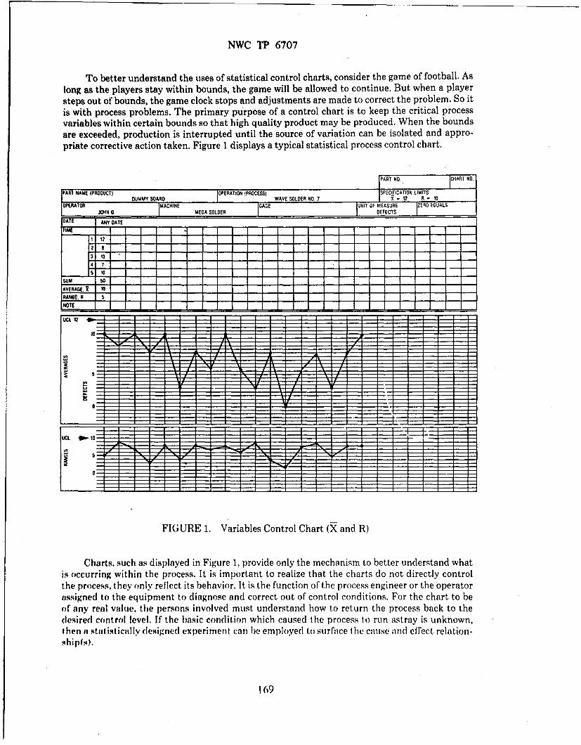
NWC TP 6707
To better understand the uses of statistical control charts, consider the game of football. Aslong as the players stay within bounds, the game will be allowed to continue. But when a playersteps out of bounds, the game clock stops and adjustments are made to correct the problem. So itis with process problems. The primary purpose of a control chart is to keep the critical processvariables within certain bounds so that high quality product may be produced. When the boundsare exceeded, production is interrupted until the source of variation can be isolated and appro-priate corrective action taken. Figure 1 displays a typical statistical process control chart.
PART NO. CHART NO.
PART NAME (PRODUCT) OPERATION ýPROCESS) SPECIFICATION LIMITSDUMMY BOARD I WAVE SOLDER NO. 7 0 -12 R - 10
OPERATOR MACHINE GAGE UNIT OF MEASURE ZERO EGUALS
DATE ANY DATE
TIME
4 1?
SUM 50
AVERAGE. J 10RANGE.R 5
NOTE
UCL 12
0
FIGURE 1. Variables Control Chart (K and R)
Charts. such as displayed in Figure 1, provide only the mechanism to better understand whatis occurring within the process. It is important to realize that the charts do not directly controlthe process, they only reflect its behavior. It is the function of the process engineer or the operatorassigned to the equipment to diagnose and correct out of control conditions. For the chart to beof any real value, the persons involved must understand how to return the process back to thedesired control level. If the basic condition which caused the process to run astray is unknown,then a statistically designed experiment can 1)0 employed to surface thle cause and efrect relation-shipifs).
169
NWC TP 6707II
PROCESS CHARACTERIZATIONProcess characterization is central to the derivation of yield and quality improvements. Before
a yield enhancement program can be initiated it is necessary to first understand what a particularprocess is actually capable of producing. Only after characterizing the process in this manner cana reasonable estimate be made of what and how many changes need to occur.
As an example, consider a wave solder process. With this particular application, it may benecessary to run 20 to 40 PWB's to develop the yield characteristics for a given set of material andequipment parameters. Resultant data should be recorded, analyzed, and graphed to provide anunderstanding of the process behavior and capability. The records generated from this effort canthen be used as a frame of reference for future process development work. The following outlinepresents the basic steps involved with process characterization efforts. 2i.General Step-Wise Progression:
a) Select the operating conditions considered best for wave soldering the PWB's.b) Run characterization study (20 to 40 PWB's). Inspect and record data.c) Construct X and R charts from the data.d) Select factors that are suspected of influencing yields, e.g. pre-heat, conveyor speed, flux type,
conveyor angle, component preparation, etc.e) Prepare a full factorial experiment to study effects of varying experimental factors. Run
duplicates for each experiment block.f) Run the experiment after randomizing the experiment sequence. Inspect the PWB's and
record the results.g) Analyze the data after the experiment is finished. This may be done either graphically, by
tabulation, or by using statistical analytical programs such as ANOVA. (Reference 4)h) Evaluate experiment results by running a confirmation test. If the results indicate that a
certain configuration of parameters provides the best results, then this configuration shouldbe tested to determine if the results are reproducible. If the results are less than desired,then additional process development is required using Evolutionary Operational Proce-dures (EVOP). (Reference 5)
EXAMPLES OF PROCESS DEVELOPMENTMany applications of statistical process development techniques have been employed at
Motorola GEG. Such applications range from evaluating PWB's from various suppliers to devel-oping wave solder parameters related to IR reflow soldering. In each of these applications GEGhas used process characterization techniques similar to that presented in the step-wise progres-sion.
STATISTICALLY DESIGNED EXPERIMENTSLet us examine the steps associated with a wave solder process optimization study. The fol-
lowing example illustrates how it is possible to differentiate between the effects of pre-solder pro-cessing, wave solder machine parameters, circuit board influences, and solder inspector differences.
In this example a new facility is just starting production with now equipment and PWB's,,"The first production test runs produced poor inspection yields with abnormally high defeots. The"primary problem involved determining how to identify the major source(s) of variation which wereresponsible for the undesirably low solder yields.
To resolve the problem, an experiment was designed, In this particular study three wave sol- rder machine variables, and two PWB in-house processing parameters were evaluated. A full fac- e kitorial experiment was employed to structure the critical variables for testing purposes. (Reference6) Each of the variables, was studied at two levels. In this particular case there were 32 different
170
_ t."2_. V-

NWC TP 6707
treatment combinations. Each of the treatment combinations or "experiments"was repeated. Thiswas done to determine the amount of experimental error associated with the tests. The experi-ment used the following parameters and levels:
Parameters Levels
Conveyor speed 2.4 and 4.2 feet/minutePreheat temperature 240 and 277 degrees F.Solder temperature 500 and 520 degrees F.Cleaning of board Clean and noncleanedBaking of board Bake and nonbaked
The matrix displayed in Figure 2 illustrates the concept of a iull factorial experiment design.It, should be noted that the matrix allowed the levels of' the variables to be crossed in such a man-ner as to allow all possible combinations of variables and levels to be explored. Herein lies thepower of the full factorial experiment.
CLEAN CLEAN NO CLEANBAKE NO BAKE BAKE NO BAKE 'BAKE
SPEED SPEED fpm SPEED pmroSOLDER PREHEAT 2.4 4,2 2,4 4,2 2.4 4.2 2,4 4,2
2771F 7021 760 762 719 716 753 718 7125201 711 751 707 714 726 703 759 724
750 708 737 721 755 744 736 7462401 742 732 741 729 783 739 728 749
9771F 725 710 706 70E 757 704 748 7646007F 781 743 758 722 747 727 717 733
2401F 745 709 701 715 731 740 723 738738 756 730 734 713 754 720 752
WHERE THE NUMBER IN THE CELLS REPRESENTS THE PANEL SERIAL NUMBER
FIGURE2. Designof'eExperiments/Full Factorialr
more.It wits determined that 95 percent cofidence would be required to justify any changes maderto the process on tile basis of the experimental findings. Consequently, an alpha risk of`5 percent'"was selected as the primary decision criteria; i.e., itf the outcomesi of the experiment stood more ..than a 5 percent. pi ,hability of being due to random chance, then the effect under consideration ,.,would he classified as statistically insignificant, '''
The outcomes of the experiment, are displayed in Figure ;3, This form of tabular data pres- .,,entation can be used to analyze the data visually for trends or outstanding results. In addition, •'suchi a cursory, examination requires no mathematical calculations. Often this method will reveal , A t%"significant information that may he used t~o direct future invest igations. The data has been pre-I isented in this format as a means of'simplifying the narrative portion of' this particular section of',,,:thle paper. I t is ant icipated t hat thle reader wi 11 recogn ize Ilie Ifact Ithat Iti~e actuLal stat ist ical analy--",ses were more than Just visuafl interpretations of the experimental data, ."
Ar.4
1additi1n,
2r"vealheen pre-0
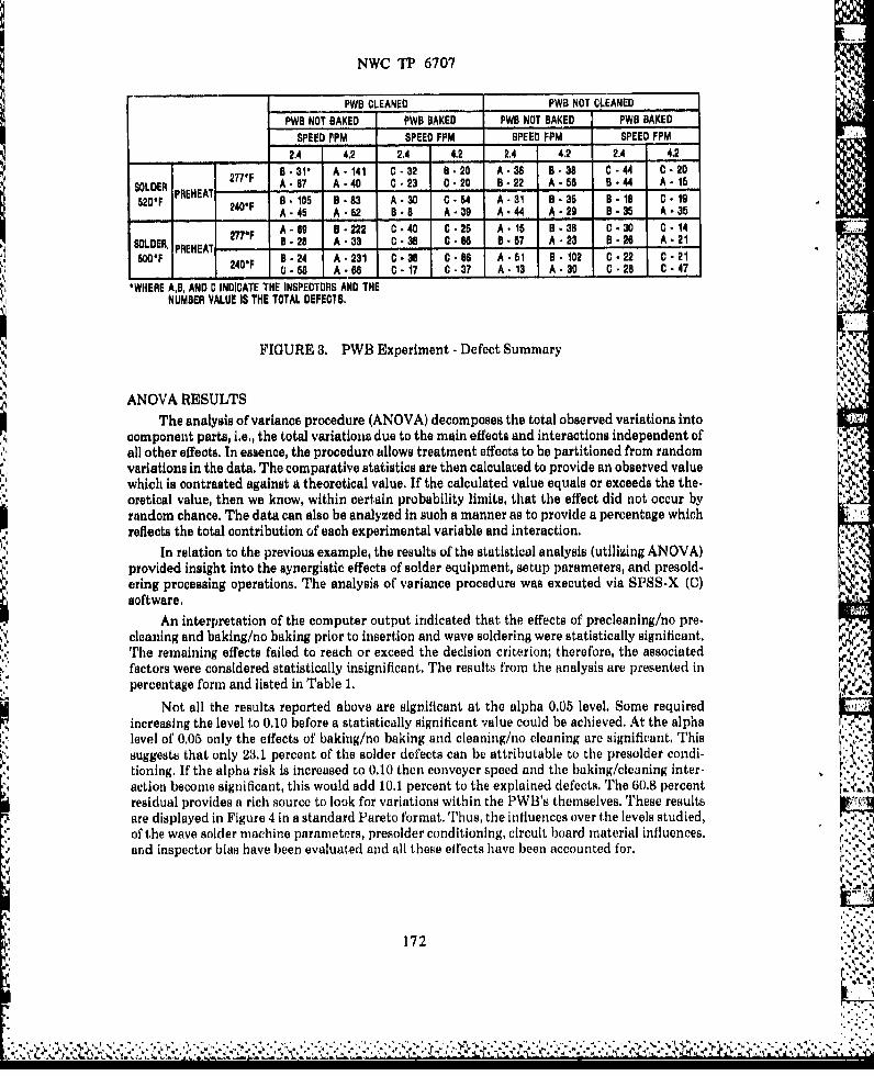
NWC TP 6707
PWB CLEANED PWB NOT CLEANED
PWB NOT BAKED PWB BAKED PWB NOT BAKED PWB BAKED
SPEED PPM SPEED FPM SPEED FPM SPEED FPM
2.4 4.2 2,4 4,2 2.4 4.2 2.4 4,2
2771.. . 31' A- 141 C- 32 9. 20 A- 36 B- 38 0 -44 C- 20SOLDER 277F A- 87 A -40 C 23 C- 20 B -22 A- 65 B -44 A - 15SOD R •EHEAT -.-- ..--.
52BP . 105 B -83 A- 30 C- 54 A- 31 B- 35 B- 18 C- 19240"F A -45 A -62 B- B A- 39 A- 44 A- 29 B- 35 A -35
A - 69 B-222 C. 40 C. 25 A- 15 0. 38 0-30 C- 14
SOLDER, PREHEA 277F B -28 A -33 0-30 C -86 B- 57 A- 23 5-26 A- 21
OO*F240F . 24 A-231 C- 3 C- 86 9. 51 B. 102 C -22 C-.21I - - A-68 0-17 C-37 A-13 A-30 .-28 C-47
L*WHERE A,B, AND 0 INDICATE THE INSPECTORS AND THENUMBER VALUE IS THE TOTAL DEFECTS.
FIGURE 3, PWB Experiment - Defect Summary
ANOVA RESULTS
The analysis of variance procedure (ANOVA) decomposes the total observed variations intocomponent parts, i.e., the total variations due to the main effects and interactions independent ofall other effectsIn essence, the procedure allows treatment effects to be partitioned from randomvariations in the data. The comparative statistics are then calculated to provide an observed valuewhich is contrasted against a theoretical value. If the calculated value equals or exceeds the the-oretical value, then we know, within certain probability limits, that the effect did not occur byrandom chance, The data can also be analyzed in such a manner as to provide a percentage whichreflects the total contribution of each experimental variable and interaction.
In relation to the previous example, the results of the statistical analysis (utilizing ANOVA)provided insight into the synergistic effects of solder equipment, setup parameters, and presold-ering processing operations. The analysis of variance procedure was executed via SPSS-X (C)software.
An interpretation of the computer output indicated that the effects of precleaning/no pre-cleaning and baking/no baking prior to insertion and wave soldering were statistically significant.The remaining effects failed to reach or exceed the decision criterion; therefore, the associatedfactors were considered statistically insignificant. The results from the analysis are presented inpercentage form and listed in Table 1.
Not all the results reported above are significant at the alpha 0.05 level. Some requiredincreasing the level to 0.10 before a statistically significant value could be achieved. At the alphalevel of 0,05 only the effects of baking/no baking and cleaning/no cleaning are significant, Thissuggests that only 23,1 percent of the solder dc'ects can be attributable to the presolder condi-tioning. If the alpha risk is increased to 0.10 then conveyer speed and the baking/cleaning inter-action become significant, this would add 10.1 percent to the explained defects. The 60.8 percentresidual provides a rich source to look for variations within the PWB's themselves. These resultsare displayed in Figure 4 in a standard Pareto format. Thus, the influences over the levels studied,of the wave solder machine parameters, presolder conditioning, circuit board material influences,and inspector bias have been evaluated and all these effects have been accounted for.
172

NWC TP 6707
TABLE 1. Results from ANOVA Analysis
Effect Analyzed Percent Variation4 in Solder Yields
Baking/no baking ................................................... 12.9%Cleaning/no cleaning ................................................ 10. 2Conveyor speed.....................................................56.1%Solder temperature .................................................. 1.7%WBoard preheat temperature............................................. 0. 2Interaction between baking and cleaning.................................... 5.0%Interaction between conveyor speed and cleaning ............................. 4.1 %Inspectors......................................................... 0.5%All other effects.................................................... 60.8%91
13 7
11 ~ % OF TOTAL VARIATION EXPLAINED
10 "IMlt
7 7
44
6 :t3 ,:;,.::*'
44 K/NO BK OLN/NO CLN SPEED BK/CLN SPDICLN SOLDER PREHEAT
44,VARIABLES 53580-6
FIGURE 4. PWB Solder Analysis .*.
173
4) ~.%

NWC TP 6707
GRAPHICAL INTERPRETATION OF RESULTSThe results from designed experiments can be examined graphically to aid in the under-
standing of the effects of the experimental factors. (Reference 7) The principle advantage ofgraphical analysis techniques is that the graphs allow a visual presentation of the effects of var-ious combinations of factors and levels. Sometimes the graphical methods offer a much clearerunderstanding of these combined effects than just pure numbers can provide, The graphical pres-entation is limited to three dimensions at a time, therefore the four factor and above graphicalpresentations of simultaneous interactions are not possible, However, the graphical analysis is avery fist tool to determine interactions and provide an overall sense of output property direction.Examples of graphical presentations are show in several applications in this paper. Two level onefactor, two level two factor, and three level two factor analysis are shown later in this presentation.Each of these graphic forms provides a different source of information. As an example of a twolevel one factor analysis, Figure 5 provides the data to assess the effects of a single factor maineffect at two levels, The example in Figure 5 is a very simple plot of the dependent variable, whichis the total number of defects obtained from the independent variable of two different conveyorspeeds across a wave solder machine,
219
200
143
100
1.0 2,0 3.0 4.0 5.0FEET/MINUTE •%
CONwVEOR SPEED
FIGURE 5, Main Effects of Conveyor Speed
FRACTIONAL FACTORIAL EXPERIMENTSFractional factorial experiments are another useful concept found in the statistical tool bag,
(Reference 8) Somewhat like a full factorial in its original structure in setting up the factors andlevels, the fractional factorial experiment differs in the number of' experiments required and theamount of data captured. The fractional factorial experiment has an advantage when used in ascreening application, and is a very useful concept when faced with a large experiment matrix,
174 ft
-L,.

NWC TP 6707
such as a seven factor at three levels. This type of experiment would result in a full factorial of
2187 different experiments, which is a rather large undertaking in any facility. But the same
experiment could be screened with 81 experiments or less to determine if the combinations selected
were providing results close to those desired. From this it can be seen that when faced with a large
range of factors and levels to evaluate, the fractional factorial experiment will save time, money,and resources, and still provide a good screening of those factors. The fractional factorial experi-
ment is developed from a specific sampling format taken from the full factorial format. The pat-
tern generated from the levels and factors provides a statistically valid sampling plan that can be
analyzed using, among others, ANOVA techniques. One of the areas of complication that tends to
arise in fractional factorial experiments is the aspect of interaction beyond the main effects. That
is, what are the contributions to the total level of effects that are attributable to the second and
third order interactions'? These interaction effects are difficult to calculate above the third order
interaction, and because of this, the higher order effects usually do not provide significant influ-
ences and therefore are considered to be negligible.
As an example of the use of a fractional factorial experiment, let us examine the followingexperiment run to minimize solder defects through optimizing wave solder machine parameters.This experiment utilizes results obtained from previous work run to determine the main factors
effecting yields from the wave solder equipment. It is from this preliminary work that the factors
and levels for this study were derived, This experiment examines six factors. Five factors exam-
ined at two levels, and one factor examined at three levels. These factors all relate to the wavesolder equipment operating parameters, The experiment matrix is shown in Figure 6.
SOLDER TEMPERATURE
4751F 6101F1
FLUX DENSITY FLUX DENSITY
0,886 0,906 0,888 0,90
SPEED FPM SPEED FPM SPEED FPM SPEED FPM
-2- 5.0-- 2,2 - .0 21 2 5.0 2.2 510'10 ' ' =o 34, lee 62 68 s
51 100 90 38
50l0o 132 57 190 44 -
32 141 38 so 88S100 27 174 128 72
- 50 73 33 52 23
" so 58 951_ 128 416"- 0 98 186 ' 85" 88
PWB PANEL SERIAL NUMBER
FIGURE 6. Fractional Factorial ExperimentWave Solder Experimentation Parameter Settings
175
.'.., ...
,
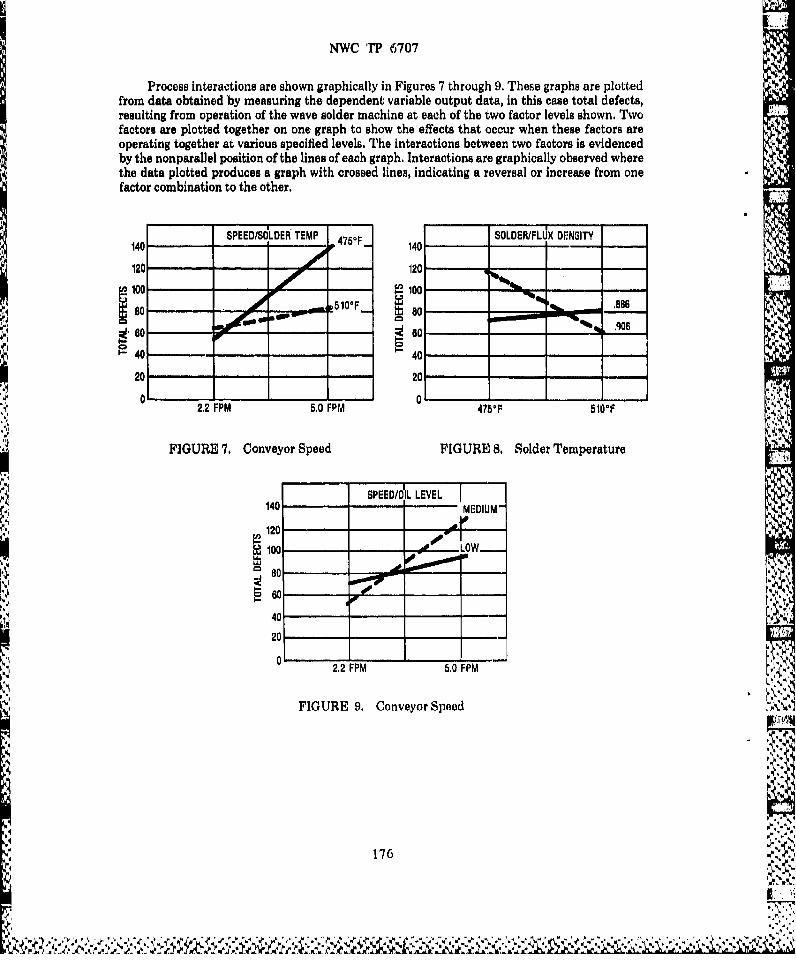
NWC TP 6707
Process interactions are shown graphically in Figures 7 through 9. These graphs are plottedfrom data obtained by measuring the dependent variable output data, in this case total defects,resulting from operation of the wave solder machine at each of the two factor levels shown. Twofactors are plotted together on one graph to show the effects that occur when these factors areoperating together at various specified levels. The interactions between two factors is evidencedby the nonparallel position of the lines of each graph. Interactions are graphically observed wherethe data plotted produces a graph with crossed lines, indicating a reversal or increase from onefactor combination to the other.
SPEEDLDE TEMP 1SOLDER/FLUX DENSITY140 475' 140 - q• l
120 120-"• 100 10. ..
so 4 -"a 510°F 80 a886
660 _-- 60 ". .906
•40 40,
20 20
2.2 FPM 5.0 FPM 475OF 5101
FIGURE 7. Conveyor Speed FIGURE 8. Solder Temperature
1SPEED/IL LEVEL I140 MEDIUM"
120 - - -7 .OW100- LOW-''U0 _
40
20(
S2.2 FPM 5.0 FPM
FIGURE 9. Conveyor Speed
176

NWC TP 6707
PROCESS CAPABILITIES PREDICTIONAn application used at Motorola, GEG, involved monitoring the gold plating on PWB's to
achieve a wire bond of consistent quality. The circuit utilized an assembly technique where sev-eral integrated circuits (IC's) were used as a part of the circuit assembly. The initial problem wasone of developing consistent wire bond pull strengths with acceptable standard deviations. Thecircuit board manufacturer had set uip a gold plating process specifically to supply wire bondable,gold plated PWB's for this design. The supplier's previous gold plating experience had been inplating edge contacts on PWB's with hard gold, which is a totally different requirement than thatof a wire bondable gold.
To solve this problem, and to help reduce the product rejects at incoming inspection,Motorola worked with the supplier to develop a process characterization of the plating process asit related to the wire bondability of the resultant plating. Samples were plated and wire bonded.These were then subjected to wire pull testing, and the data was evaluated to determine the pro-jected process capability. A computer program was generated to analyze the results of the wirepull tests. Wire pull data was entered into the computer and the resultant statistical informationprinted out the projected wire bond limits that could be expected from the circuits in that lot,based on a 95 percent confidence limit. This printout also provided an accessment with a known
probability of what percent of the product that would fall below the lower acceptance limit, shouldthere be any in that category, Figure 10 is a graphical presentation of the range of wire bond pullstrength values derived from a normal distribution, based on the infbrmation obtained in lot sam-ple testing. In this particular case there is a 95 percent probability that 1,1 percent of the productwill be below the 2.0 gram limit, therefore rejecting the test lot. Figure 11 is a close-up of the tailof the lower limit of the distribution as shown in Figure 10.
The examples shown in Figures 10 and 11 were very instrumental in measuring the overallimprovements in the development of the plating processes. Thase concepts are not new, they sim-ply illustrate the power and information that is resident in statistical procedures that already exist.Statistical calculations may provide meaningful data from even the simplest of formulas.
PROCESS AVE:RAGE 7T6 QMS
-,-'' ~~SPECIFICATION •,'LOWER LIMIT /• -,
S~,.*.;
3y7.8 GMSbLOWER AVERAGELIMIT1.5 GMS
FIGURE 10. Distribution of Wire Pull Strengths
177
.t'
w,..

NWC TP 6707
1.1% OF PRODUCTCOULD BE FOUNDIN THIS ,
• , PROCESS LOWERA I' SPECIFICATION
LIMITLOWERLIMIT1,6 GMS
FIGURE 11, Detail of Lower Limit Tail
Another example of the use of comparative statistics is the application where one wishes todetermine if there are significant differences between groups of data. Let us consider a wave sol-
der line that has been producing yields that appear to be quite variable, There is an unfoundedsuspicion that the variation In wave solder quality is caused by wave solder machine set up param-eters varying during the production run. This is a good example of how raw results can be quitedeceiving, for as we shall see, it takes more than a casual examination to obtain the facts. Uponlooking into this problem, mixed lot date codes were found on the PWB's used in the wave solderproduction runs. The lot to lot variation in the PWB's indicated a potential for a significant con-tribution to this variation in wave solder yields. To check this hypothesis, a series of wave soldertests was run on sample PWB's selected from one supplier's lot of date code boards. If the wavesolder equipment was randomly varying from its operational parameters, then these effects shouldbe found in the solder quality of boards from a known "good"lot. The experiment was set up toevaluate wave solder machine operating parameters on three different days during a weeks pro-duction operation. These three days would also be separated from one another by at least onedays production. This allowed the worse case conditions to occur, in that it also included anequipment tear down and set up. 16 PWB's were scheduled for this experiment; six used for thefirst day, four for the second, and six for the third day. All the PWB's were run using a given setof operating parameters. With the daily changes in set-up that happen as a normal occurrence, 7.there would be ample opportunity for the effects of nonreproducibility of equipment set-up tooccur if it indeed was the significant contributing factor to the solder yield variations. To coun- ,teract time related effects, all the circuit boards were run within a specific time period each time.The boards were inspected by the same inspector after cleaning, and the defects were recorded,After all three groups were inspected the results were examined. At first glance it appeared as ,'4j
though there was a significant difference in the results, for one days group "clearly looked bet-ter"than the others. But upon statistically examining the results with a Student t analysis, it wasshown that there was no statistically significant difference between the three groups of data. (Ref-erence 9) The results of this experiment are shown in Table 3. The analysis of the results from,.
178 ".t
4'.

KW TF 7U
this experiment indicated that the equipment was not the single source of the problem of varyingyields, and that the production groups with the mixed lot date codes should be examined to deter-mine their effect on yields.
TABLE 3. Results From Solder Inspection
Group 1 Group 2 Group 3
Sample size -- PWB's 6 4 6Insufficient solder 2 0 0Excess solder 2 6 9Poor Wetting 27 13 15Blowholes/depressions 37 16 26Shorts 5 0 1
RANDOMLY SELECTED TEST COMBINATIONSThis experimental design method was used to examine the effects of inert gas flow rates in a
six zone IR reflow furnace. The effects of gas flow on the zone temperatures was an unknown fac-tor in setting up the IR reflow equipment. To resolve this question an experiment utilizing a ran-domly selected test combination technique was initiated. (Reference 10) This experiment designis a screening tool used in cases where there is a large number of factors and levels in an experi-ment matrix. This test method generates the experiment matrix from a balanced combination oftest factors. The resulting total number of experiments is usually less than a fractional factorial,although this is not a fixed rule. Normally, the sample size is 1 to 5 percent of the size that wouldresult from the full factorial experiment. This experiment design has an inherent disadvantage inthat the confidence levels cannot be established in estimating the effects of factors. This is due tothe fact that the data generated from the experiment can only be analyzed graphically for trends.The main effects produced in the experiment are observed as the steepest slope plotted. The effectsof the most significant factor(s) can be removed mathematically to reveal the next most signifi-cant factor. This may continue until all the significant factors have been tagged. This process canvery quickly provide information that will allow a more appropriate selection of factors and levelsto be run in a follow on experiment, thus enhancing an optimized result.
In the case of the IR reflow experiment there were eight factors at three levels that wouldresult in 6561 experiments in a full factorial format. This experiment used only 99 samples to screenall factors. The results from this experiment are being evaluated at this time. The initial findingsappear to suggest that the inert gas flow rate is not a significant factor and the reflow zone tem-peratures are not effected by varying flow rates. The most significant factor appears to be con-veyor speed.
Figure 12 is shown as a demonstration of the graphics analysis to show the interrelationshipsof independent factors. The independent variables shown on the X and Z axis in this example arethe inert gas flows into the reflow zones and conveyor speed. The dependent variable in the Y axisis the resultant temperature in the reflow zones. This graph shows a two factor three level resultof the effects of inert gas flowing through the reflow zones of an IR reflow machine.
179

NWC TP 6707
~'-270-C
"-220-0 PEAK TEMPERATURES INREFLOW ZONEDEGREES C
*.00CUBIC EET PE
1-80
I' .. *'S 4' *..I .* **~ .. . ..~~'* '" '* *'~ . * .\.'¶.~ **" ' *0 ~.,0 Z*

NWC TP 6707
CONCLUSIONS
The applications presented in this paper represent only a few of the experiments that havebeen run at Motorola, GEG. The results obtained from these experiments have provided valuableinsights into many complex problems,
The statistical methods presented in this paper have greatly benefited Motorola's under-standing of the complexities of inter- related factors effecting PWB wave soldering. Prior to theimplementation of statistical analytical methods the combined effects of materials, pre-processconditionings, and process induced interactions, created a confusing array of possible solutions,and required considerable time and resources to find an appropriate solution. Through the use ofthese analytical and statistical principles, complex problems can now be resolved in a timely man-ner with moderate usage of resources, Wave solder process characteristics can now be formallydocumented to provide a meaningful assessment of process changes,
The techniques presented in this paper are not intended to represent the only analysismethods that may be used, rather they are only a small sampling presented to show the applica-tion variety. There are many other methods that may be used to provide answers to process relatedquestions. The examples shown in this presentation have been some what limited to PWB appli-cations and wave solder evaluations, However, this does not mean that these are the only appli-cations for these principles. The statistical design concepts and analytical techniques pre43entedhere could be used to make significant contributions in design engineering applications withreduced development time, potentially lower overall development cost, and optimized designs asan output of their use.
The concepts of statistical process control continue to be pressed into more extensive appli-cation as the training spreads throughout the GEG facility. These techniques will ultimatelybecome the order of the day, rather than the exception, for the daily operation of all Motorola,GEG, Tactical Electronics Division (TED) projects.
Bibliography
1,-Irving Adler, Probability and Statistics for Everyman, First Edition. The New Amer.icon Library, New York, N. Y., 1966
2,- D, W, Thomas Chairman, Statistical Quality Control Handbook, Ninth Printing, Del-mar Printing Co., Charlotte, N,C., 1984
3,- Ford Motor Company, Continuing Process Control and Process Capability Improve-mnent, Ford Motor Company, 1983
4.- Douglas C, Montgomery, Design and Analysis of Experiments, Second Edition, JohnWiley and Sons, New York, NMY., 1984
5.- Douglas C. Montgomery, ibid.
6,- Charles R, Hicks, "Fundamental Concepts in the Design of Experiments," ThirdEdition, Holt, Rinehart, and Winston, New York, N. Y., 1982
7,- Douglas C. Montgomery, ibid.8.- Charles R. Hicks, ibid. * ."p.9.- Norman R. Kurtz, Introduction to Social Statistics, Mc (Graw-Hill Book Company,
New York, N, Y., 1983
10.- Charles Lipson and Narendra.J, Sheth, Statistical Design and Analysis of Engineer-ing Experiments, Mc GrawHill Book Company, New York, N.Y., 1973
%\
181
"" ".

NWC TP 6707 II Larry Lichtenberg is Senior Product Engineer with
Motorola's Government Electronics Group. He has 18years experience with Hybrid and Printed Wiring BoardAssembly, and is involved in all phases of soldertechnology-from research projects to processdevelopment. He is a member of the American ChemicalSociety and the Inteenational Society for Hybrid MicroElecti onics. He holds a BS degree in Chemistry, which hereceived in 1982 from Northeast Missouri State ~ .
8220 E. Roosevelt Rd.
ScottsdAle, AZ 85252
t. ."41
182

NWC TP 6707
REAL TIME AUTOMATED INSPECTION
OF SMD) SOLDER JOINTS
by
Todd LaMarcheMarketing A lications Specialist
Nicolet Instrument Corporation/Mikrox GroupMadison, Wisconsin •,
ABSTRACT
The historic dilema of Process and Quality Control lies in the balance between yield
loss and customer rejections vs time, consumables, and extra personnel required fortesting. How much time can be gained from a given investment in additional equipmentand operating expenses?
The new process control tool, micro-focus real-time radiography, addresses all ofthe traditional drawbacks of testing while providing more information. Testing isaccomplished, non-dastructively, with no sample preparation, on the production floor withproduction personnel.
Thus, process deviations am detected, quantified, and appropriate adjustments aremade or unsalvageable problems are rejected early in the process. Applications span allaspects of the electronic industry; semi-conductor, hybrid circuit, discrete component, •,multi-layer PCB and surface mount technology. The ability to see high atomic numbered
structures as small as .001" encapsulated in lower density materials are preferredapplications. Nicolet Instruments Mikrox system addresses these inspection needs.
THE X-RAY PROCESS
A mixture of technology is required to develop real-time x-ray imaging. TheNicolet Mikrox system has the ability to magnify from 20 to 50 times like a microscope andpeer inside objects like and x-ray machine. The X-ray tube operation consists of electronsbeing boiled off the filament of the cathode and striking a tungsten target on the anode,thereby creating x-radiation. The penetrating power of the x-rays is determined by thekilovoltage applied to the potential difference between the anode and cathode.
To complete the x-ray process at least a portion of the radiation must pass through asample in order to create an image on film or on an x-ray sensitive camera ( used for real-
183
I..
A,... - ,- .4 ¾ *
.. .,..44. :,, .1
4,.. *, • . ,I *%•., . *..• -, , .. .. .,. .. ,, ', . ,; ' :/ .- ' '." ., ' .' ... " , ' . .... ,..'......*..,. .... , ., ., .. *-. -..

LawNWC TP 6707
time viewing). More radiation will pass through a void (flaw) or lack of material and willshow as a lighter area on a video display. Areas that are more dense and absorb moreradiation will appear darker.
The unique resolution characteristics of Mikrox are partially attributed to the finitesize of the focal point from which the x-rays are generated. This focal spot measuresapproximately 10 microns.
SMT INSPECTION REQUIREMENTS
The ability to establish and monitor SMT process parameters is absolutely retardedwithout the ability to visualize the condition of the solder connections beneath the surface-mounted component. Five specific problems which are most common during the surfacemount process can be detected with x-ray imaging.
- Solder BallsSolder BridgingSolder Voids
- Lack of Solder & Poor Fillet- Component Misregistration
REAL-TIME X-RAY APPLICATIONS
Generally four levels of inspection are addressed through x-ray imaging.
- Failure analysis for laboratory use in establishing quality parameters andmonitoring at a research an development level. Rotational capabilities allow formultiple viewing angles of the specimen.
- Medium .poduction level and on-line process control. A manually controlledsystem with x-y movement and large area of view for monitoring all levelsdiring the manufacturing process.
Automated with x-y programmability. A system requiring operator judgementcan be networked with other intelligent equipment such as rework and repairsituations and drill equipment.
Automatic with image recognition. Computer aided decision maidng isintegrated to the automatic system with x-y programmability.
AUTMATED INSPECTION
There are many reasons for needing an automated system, (high volume, 100%inspection, programmability, repeatability, networking), but it all boils down to one issue:the need for an effective, accurate means of controlling the manufacturing process.
An automated system with the above features can accomplish this task, but still
requires human judgement.
184
.'f:- Zr Wý

r t rNWC TP 6707
Through the integration of automatic image recognition, the on-line operatorrequirement is eliminated. By taking the electrical output of the x-ray sensitive camer, acomputer evaluation can be made.
Driven by a 68010 microprocessor, the vision system can inspect appro.'.ately 1"square of populated every 4 seconds. Problems detected are quan. led, x-y position isdefined and the reporting cycle is completed through hard copy printouts, or electnicstorage of the data. Thus, an automated system provides continuous, closed loop feedbackto pre and post manufacturing processes.
V.
iL
5 .I:4'
,5 •.a
•" r• ,'41
•'U•
A' [ •..*~
-:,:. .*i . * h 'i

NWC TP 6707
Todd LaMarche is Marketing Applications Specialistwith Nicolet Instruments. He has 15 years experience inmanufacturing engineering and process engineeringsupport, spscializing in circuit board assembly processes.
Address: Nicolet Instruments Corp.5226-5 Verona Rd,P.O. Box 4370Madison, WI 53711-0508
186...S
L.o
186 """
• .• . . . .. 'I o'
NWC TP 6707
CIRCUIT CARD ASSEMBLY INSPECTIONOF SURFACE MOUNT COMPONENTS
UTILIZING A MACHINE VISION CONTROLLER
by
M. G. (Mike) Buffa
Vice President, Electronics Systems DivisionMachine Vision International
Ann Arbor, Michigan
January 5, 1986
ABSTRACT !.N.
This paper describes the benefits and operation of amachine vision controller for surface mount technologyprocess control. The paper outlines economic benefitswith an example of savings realized by machine visiondetection of defective assemblies before they reach thefield. A description of the vision controller's functionat each step of the assembly process shows how feedbackto process control provides short process correctiontime, reduction in repair and labor costs, increasedyield and improved quality control.
187
"."•,.er
'-I" "-b
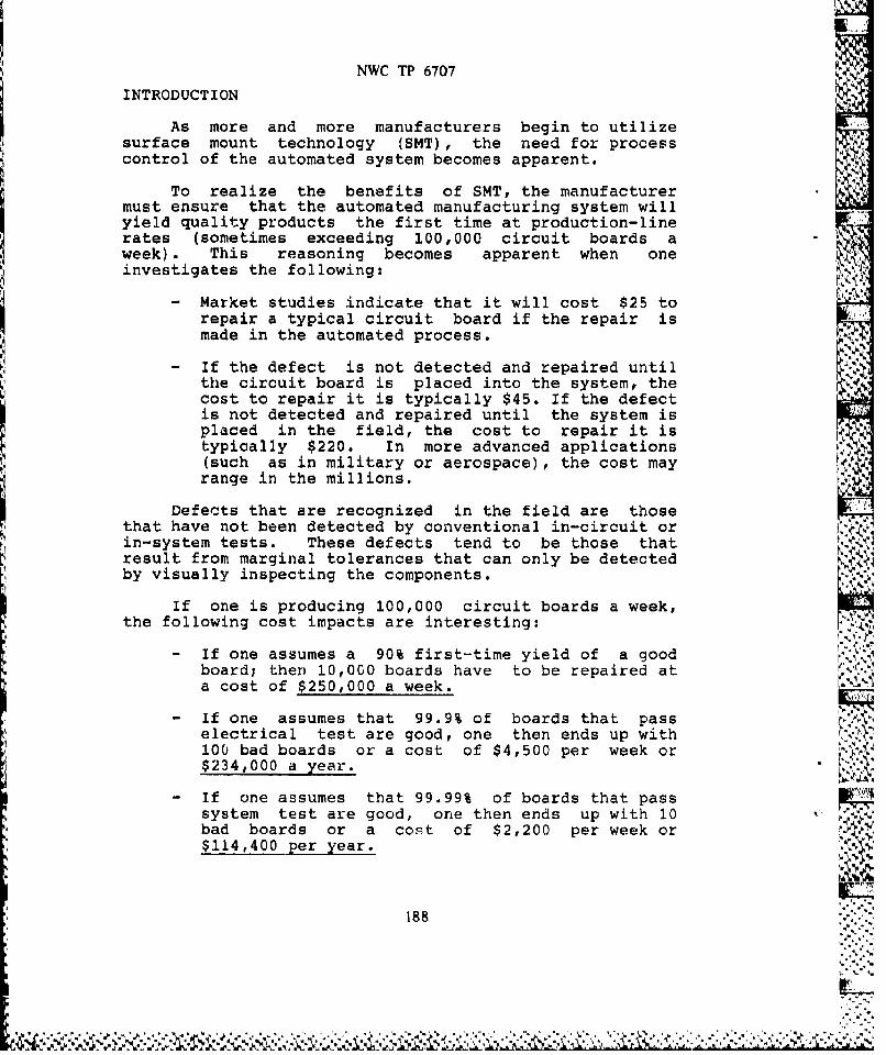
NWC TP 6707
INTRODUCTION
As more and more manufacturers begin to utilizesurface mount technology (SMT), the need for processcontrol of the automated system becomes apparent.
To realize the benefits of SMT, the manufacturermust ensure that the automated manufacturing system willyield quality products the first time at production-linerates (sometimes exceeding 100,000 circuit boards aweek). This reasoning becomes apparent when oneinvestigates the following:
- Market studies indicate that it will cost $25 torepair a typical circuit board if the repair ismade in the automated process.
- If the defect is not detected and repaired untilthe circuit board is placed into the system, thecost to repair it is typically $45. If the defectis not detected and repaired until the system isplaced in the field, the cost to repair it istypically $220. In more advanced applications(such as in military or aerospace), the cost mayrange in the millions.
Defects that are recognized in the field are thosethat have not been detected by conventional in-circuit orin-system tests. These defects tend to be those thatresult from marginal tolerances that can only be detectedby visually inspecting the components.
If one is producing 100,000 circuit boards a week,the following cost impacts are interesting:
If one assumes a 90% first-time yield of a good . .•
board; then 10,000 boards have to be repaired ata cost of $250,000 a week.
electrical test are good, one then ends up with
100 bad boards or a cost of $4,500 per week or$234,000 a year.
If one assumes that 99.99% of boards that passsystem test are good, one then ends up with 10 , .bad boards or a cost of $2,200 per week or$114,400 per year.
188

NWC TP 6707
From this analysis, it becomes apparent that themost important aspect of manufacturing the product is toensure maximum first-time yields and to minimize the highcost associated with repairing the circuit board later.
Utilization of machine vision controllers in theprocess will ensure a major decrease in production andrepair costs by:
* °- Dramatically improving first-time yields
- Dramatically reducing the overall defects notdetected by electrical testing
SYSTEM OVERVIEW
FIGURES 1 and 2 outline the typical SMTmanufacturing process and associated process controlissues.
The overall system utilizes a host computer and aseries of distributed machine vision controllers (MVC)that incorporate an Image Flow Computer, personalcomputer, camera positioner, and man/machine interface.The MVC is used to monitor and control each majorsubsystem in the overall process. These subsystemstypically are:
- Solder Paste Deposition •'!..
- Component Placement (sometimes multiple) -.
- Solder Reflow ,. ,A
HOST SYSTEM
The host system monitors and controls the overall
performance of the system.
The host performs the initial line setup whereby the
circuit board set-points are sent to the MVC. Suchset-points would include:
- Solder Paste Amount and Location
"- Component Types and Locations- Final Solder Amounts- Final Component Locations .- Set-Point Alarm Tolerances- Alarm Limits
189
.4'.:
.A -A *

NWC TP 6707
SMO Board Coordinate System
iComponents
Flow Work It
FIGURE I "
190
L• qi 4
-F-i<
Flow'of Work
) l"FIG-RE "

NWC TP 6707
'a. j4JOIs
.5- C,
E. E
*1 *0
M~O
C,4u~ I 9i

NWC TP 6707
The host would also monitor trends in the process sodynamic corrections may be made to the process if systemvariables are reaching alarm limits. In extreme cases,the host may decide to shut down individual pieces ofequipment if they exceed critical tolerances. Such anexample may be an in-line process where there is no humaninvolvement.
SOLDER PASTE DEPOSITION
The MVC would inspect the circuit board to ensure:
That pattern registration is withinspecification, precisely measuring offsets toreference locations so pads can be located forlater use in the process.
That the solder paste is located properly and is.'.i ~~the right amount.[i'•
If deviations are noted from set-point tolerances,corrective action can be taken by the host or the screenprinter.
If board registration is out of specification, the
board would be diverted out of the process.
COMPONENT PLACEMENT
The MVC will be utilized to inspect each circuit
located properly.
In the case of chip capacitors, chip resistors oractive devices that are placed by high-speed pick andplace units (3-6 parts per second) the MVC will inspectto tolerances of 3-10 mils to ensure that the componentis positioned properly on the pad.
The MVC utilizes high-speed morphological grayscaleoperations to ensure that the leads are covering a givenpercentage of the pad. It should be noted that thesystem will have an accurate position for each pad as fedforward from the initial MVC. Likewise, it can beassumed that the solder paste is positioned properly andthat the position of the solder paste is known relativeto the pad.
192
...... . *'..* .... * .. f

NWC TP 6707
If a component is positioned improperly on the pad,the precise location of the centroid of the component canbe measured utilizing a high-speed "connected component"algorithm. This positional data can then be fed back tothe pick and place unit and to the system host.
For active components (usually 50 mil lead spacingor less) placed by robots (1-2 parts per second) or otherpick and place units, the MVC will do a high-resolutioninspection (1 mil tolerance) to ensure that individualleads are precisely located on pads.
For components with leads that have very finespacing (25 - 40 mils), it would be recommended that theleads be inspected for coplanarity and spacing beforebeing placed.
The location of the pads and solder paste is fedforward from the initial MVC such that the inspectiontask becomes that of locating the individual leads to agiven board (system) reference. If the device has beeninspected for coplanarity and spacing before placement,the system will not be required to inspect all of theleads on a given device.
It is also noted that a more detailed inspection ofthese active devices is necessary to ensure that partnumbers and polarities are correct.
If system tolerances are violated, then correctiveaction can be taken.
FINAL INSPECTION
The MVC will be utilized to ensure that components didnot shift during the reflow process and violate givenset-points.
The system will inspect individual pad locations toensure that the proper amount of solder is present andthat there is no excessive bridging between pads.
As before, the individual pad locations are known and canbe used in this analysis.
193
,,, , , • •"" •i '"", .. W" " '/ ' " i": "f • :>

NWC TP 6707
The MVC also can be integrated with an X-ray unit toprovide grayscale images of individual solder, joints inorder to do a detailed inspection of individual solderjoint for:
- Shape- De Wetting- Internal Voids
LEAD-nTHRU-THE-HOLE INSPECTION
"lead-thru-the-hole" (LTH) technologies with the SMTprocess.fpso
In such processes, the SMT devices will be mountedon the same side of the board as the leads before wavesoldering.
In this process, the MVC would also inspect theleads for: M
- Absence or Presence- Length- Clinch Angle
Individual repair loops can be provided at each
subsystem so defective boards can be isolated andrepaired quickly.
Quick identification of errors can be done bydirecting a light beam to the defect or by providing agraphical output to the repair person indicating thelocation of the defect.
Component misplacement or absence will beaccomplished utilizing robotics with feedback from theMVC.
194
.4194 " "
U- ;k

NWC TP 6707
JUSTIFICATION
If one assumes that this process control systemimproves the first time yield to 95%, the weekly cost isreduced $125,000, notwithstanding the other cost benefitsassociated with:
- Faster Correction Time in Process- Reduction in Repair Costs
S- Reduction in Labor Costs
The operators safety would also be improved because theywould be removed from the manufacturing process.
4'
195
4',%,,
A.I ,(
*,4
K ,* 4 * ~ ** ~ ~ A , ~ A ~ jA~ A * *,*' *A,
A~~A~'A :A A A*A A A.~AA ~:~. ~ A ~ A. A* * A -4 ' ~ ,*** A 4 * A * A * A A, A *

I
NW TP 6707-
Mike Buffa attended West Point and received a BSEEdegree from West Virginia University in 1968. Duringhis 10-year career with General Electric and Honeywell,he worked in the field of industrial automation, Hisactivities included control system design programming,project management, and management of a technicalsupport group for the Honeywell Corp, in Europe. Hisengineering experience involved the automation of
refineries, steel mills, nuclear power plants, pulp andpaper mills, and chemical plants, As Vice President ofthe Electronics Systems Division for Machine VisionInternational, he is pioneering machine visiontechnology for various applications in the electronicsindustry.
Address: Machine Vision International325 E. EisenhowerAnn Arbor, MI 48104
I.,,
I0
196
' ?i-L4*. . . . .- - -: - . - • .. .; - - " • " ; .. •. .. . ] ~ - 'I-,: u a
: - • u u• I I I r • I I l • !I ,I ,

NWC TP 6707
I ~'U
NAVY SOLDERING TECHNOLOGY TRAINING PROGRAM
by :WM. E. SAKE
Training DirectorNaval Weapons Center
Soldering Technology BranchCode 3681
China Lake, CA 93555-6001
ABSTRACT
Many changes have taken place recently and are continuing to takeplace in the field of electronic assembly and production. Key changesaffecting manufacturers of Government hardware include the issuing ofnew and revised Standards and Specifications pertaining to electronicassembly, fabrication and soldering processes. The new Standards and ."Specifications necessitate revisions within the Soldering TechnologyTraining Program to incorporate the changes. This presentation will
4 •provide a status report on current and planned revisions Lo the trainingprogram. A detailed discussion of new training courses, new certifica-tion levels and additional training sites will be provided. Implementa-tion plans and schedule for the field recertification of instructor/"examiner personnel will also be covered in detail.
197
", "' , , , " .,.'L . •,..',,.• ' •,• • , . . " "*", 4•. -' ".""". ",.. .""". . '•"" . ,-" ". , "."." ". , .-.". ''' "

NWC TP 6707
TRAINING PROGRAM STATUS OUTLINE
NAVAL WEAPONS CENTER ROLE
SOLDERING TECHNOLOGY ORGANIZATION
SOLD'ERING TECHNOLOGY TRAINING
TRAINING COURSES
Courses Offered
Course Revisions
New Courses
CERTIFICATION/RECLERTIFICATION
New Certification Levels
Operator/Inspector Recertification
Field Recertification Implementation
TRAINING PLAN REVIEWS
NEW/REVISED SPECIFICATIONS
NAVMAT Instruction 4855.10
WS-6536 Revision "E"
DOD-STD-2000
NEW TRAINING SCHOOLS
198
Best Available Copy

NWC TID 6707
William E. (Bill) Sake, NWC's own Director of SolderingTechnology Training, has 25 years experience inelectronics, with 16 years in education and productassurance for electronic assembly and solderingprocesses. Bill developed and authored the training andcertification program used by all naval aviation militaryactivities for electronic assembly soldering and repairprocesses.
Address: Code 36814Naval Weapons CenterChina Lake, CA 93555-6001
S est Available Copy