0:; ' # '8& *#0 & 9 - intechcdn.intechopen.com/pdfs-wm/40170.pdf · chapter 0...
TRANSCRIPT

3,350+OPEN ACCESS BOOKS
108,000+INTERNATIONAL
AUTHORS AND EDITORS114+ MILLION
DOWNLOADS
BOOKSDELIVERED TO
151 COUNTRIES
AUTHORS AMONG
TOP 1%MOST CITED SCIENTIST
12.2%AUTHORS AND EDITORS
FROM TOP 500 UNIVERSITIES
Selection of our books indexed in theBook Citation Index in Web of Science™
Core Collection (BKCI)
Chapter from the book Simulated Annealing - Single and Multiple Objective ProblemsDownloaded from: http://www.intechopen.com/books/s imulated-annealing-s ingle-and-multiple-objective-problems
PUBLISHED BY
World's largest Science,Technology & Medicine
Open Access book publisher
Interested in publishing with IntechOpen?Contact us at [email protected]

Chapter 0
Simulated Annealing to Improve AnalogIntegrated Circuit Design: Trade-Offs andImplementation Issues
Lucas Compassi Severo, Alessandro Girardi, Alessandro Bof de Oliveira,Fabio N. Kepler and Marcia C. Cera
Additional information is available at the end of the chapter
http://dx.doi.org/10.5772//45872
1. Introduction
The design of analog integrated circuits is complex because it involves several aspectsof device modeling, computational methodologies, and human experience. Nowadays,the well-stablished CMOS (Complementary Metal-Oxide-Semiconductor) technology ismandatory in most of the integrated circuits. The basic devices are MOS transistors, whosemanufacturing process is well understood and constantly updated in the design of smalldevices. Detailed knowledge of the devices technology is needed for modeling all aspectsof analog design, since there is a strong dependency between the circuit behavior and themanufacturing process.
Contrary to digital circuits, which are composed by millions (or even billions) of transistorswith equal dimensions, analog circuits are formed by tens of transistors, but each one witha particular geometric feature and bias operation point. Digital design is characterized bythe high degree of automation, in which the designer has low influence on the resultingphysical circuit. The quality of the CAD (Computer-Aided Design) tools used for circuitsynthesis is much more important than the designer experience. These tools are able to dealwith a large number of devices and interconnections. Digital binary circuits have robustnesscharacteristics in which the influence of non-linearities and non-idealities are not a majorconcern. Furthermore, mathematical models of devices for digital circuits are relaxed andcomputationally very efficient.
On the other hand, analog design still lacks from design automation. This is a consequenceof the problem features and the difficulty of implementing generic tools with high designaccuracy. Thus, the complex relations between design objectives and design variables resultin a highly non-linear n-dimensional system. Technology dependency limits the designautomation, since electrical behavior is directly related to physical implementation. In
©2012 Girardi et al., licensee InTech. This is an open access chapter distributed under the terms of theCreative Commons Attribution License (http://creativecommons.org/licenses/by/3.0), which permitsunrestricted use, distribution, and reproduction in any medium, provided the original work is properlycited.
Chapter 13

2 Will-be-set-by-IN-TECH
addition, the large number of different circuit topologies, each one with unique details, makesmodeling a very difficult task.
In general, the traditional analog design flow is based on the repetition of manual optimizationand SPICE (Simulation Program with Integrated Circuit Emphasis) electrical simulations.For a given specification, a circuit topology is captured in a netlist containing devices andinterconnections. Devices sizes, such as transistors width and length, or resistors andcapacitors values, are calculated manually. The verification is performed with the aid of SPICEmodels and technology parameters in order to predict the final performance in silicon. Specificdesign goals such as dissipated power, voltage gain, or phase margin are achieved by manualcalculation and then re-verified in simulation. Once the final performance is met, the designis passed on to a physical design engineer to complete the layout, perform design rule checks,and layout versus schematic verification. The layout engineer passes the extracted physicaldesign information back to the circuit designer to recheck the circuit operation on the electricallevel. When physical effects cause the circuit to miss specifications, several more iterations ofthis circuit-to-layout loop may be required. This process is repeated for each analog block inthe circuit, even for making any relatively simple specification change. The amount of timeand human resources used can vary, depending on the design complexity and the designerexperience. However, even for a large and most skilled design team, the short time-to-marketand strict design objectives are key issues of analog designs. Improvements in the analogdesign automation can save design time and effort.
In this chapter we analyze the Simulated Annealing (SA) meta-heuristic applied to adjustcircuit parameters in transistor sizing automation procedure at electrical level. Previous workshave been done in the field of analog design automation to enable fast design at the blocklevel. Different strategies and approaches have been proposed during the evolution of analogdesign automation, such as simulation-based optimization [5, 9, 17], symbolic simulation [10],artificial intelligence [6], manually derived design equations [4, 21], hierarchy and topologyselection [11], geometric programming [12, 16] and memetic algorithms [15]. The maindifficulty encountered for wide spread usage of these tools is that they require appropriatemodeling of both devices (technology dependent) and circuit topologies in order to achievethe design objectives in a reasonable processing time.
Moreover, the option of choosing different circuit topologies is also difficult to implement ina design methodology or tool, since most approaches work with topology-based equations,limiting the application range. The possibility of adding new block topologies must also beincluded in the methodology, since it is critical to the design. The usage of optimizationalgorithms combined with design techniques seems to be a good solution when applied tospecific applications. This is because a general solution most often proves to have shortcomings for fully exploiting the capabilities of the analog CMOS technology. The keyrequirements of an analog synthesis tool are: interactivity with the user, flexibility for multipletopologies and reasonable response time. The interface with an electrical simulator and witha layout editor is also convenient [8].
The remaining of this chapter is organized as follows. Section 2 explains the SimulatedAnnealing meta-heuristic, its parameters, and functions. Circuit modeling, as well as theparameters and functions involved, are described in Sec. 3. Afterward, Sec. 4 presents a basiccircuit used to explain the usage of SA, how the searches occur, and the results achieved. InSec. 5, Simulated Annealing is used to seek solutions to a more complex circuit, in whichwe could analyze the impact of SA parameters and functions as a mean to automate circuitdesign. Finally, Sec. 6 conclude this chapter with our final remarks and future works.
262 Simulated Annealing – Single and Multiple Objective Problems

Simulated Annealing to Improve Analog Integrated Circuit Design: Trade-Offs and Implementation Issues 3
2. Simulated annealingThe Simulated Annealing (SA) is a well known random-search technique that exploits ananalogy with the way a metal heat and slowly freezes into a minimum energy crystallinestructure, the so called annealing process. In a more general system, like an optimizationproblem, it is used for searching the minimum value of a cost function, avoiding gettingtrapped in local minima. The algorithm employs random searches which, besides acceptingsolutions that decrease (i.e. minimize) the objective cost function, may also accept some thatincrease it. The latter are called “indirect steps”, and are allowed in order to escape from localoptima.
The SA algorithm uses a cooling function T(t), which maps a time instant t to a temperatureT, decreasing T as t increases. At each iteration, new steps are randomly taken, based on aprobabilistic state generation function g(X), leading to new states in the solution space. In thiscontext X is a vector of d parameters, where d is the dimensionality of the solution space. Ifa step leads to a state with a worse solution, it is only effectively taken, i.e. the new state isaccepted, with a probability less than 1. States with better solutions are always accepted. Thisprobability is given by an acceptance function h(ΔF):
h(ΔF) =1
1 + exp(ΔF/T)(1)
Here, ΔF = Ft+1− Ft represents the variation of the cost function calculated at two consecutivetimes steps Ft+1 and Ft.
The algorithm is able to reach an optimal solution on the choice of the cooling function andprobabilistic state generation function. If the temperature in cooling function decreases too fast,the search will run faster, but the SA algorithm is not guaranteed to find the global optimumanymore [13]. This may be acceptable if a solution is needed in a small amount of time andthe solution space is well-know or presents high dimensionality. This is called SimulatedQuenching (SQ) [1], and is useful when an approximate solution is sufficient. There aresome common sets of options to choose from when implementing an SA algorithm. Theyare described below.
2.1. Boltzmann annealing
The Boltzmann annealing is the classical simulated annealing algorithm, using physicsprinciples to choose the probabilistic state generation function in order to ensure convergenceto a global minimum. It employs a Gaussian distribution for generating new states:
gBoltz(X) =1
(2πT(t))d/2 exp (− (ΔX)2
2T(t)) (2)
Here, ΔX = X− X0 and d is the number of dimensionality of the search space. The Boltzmancooling function is described as:
TBoltz(t) =T0
log (t)(3)
where T0 is the initial temperature, and t is the time step.
Geman and Geman in the classical paper [7] have proved that using Gaussian distributionto generate new states (Eq. 3) with the Boltzman cooling function (Eq. 2) is sufficient to reachglobal minimum of an optimization function at infinite time.
263Simulated Annealing to Improve Analog Integrated Circuit Design: Trade-Off s and Implementation Issues

4 Will-be-set-by-IN-TECH
2.2. Fast annealing
Fast Annealing is a variant of the Boltzmann Annealing [20] that uses as probabilistic stategeneration function the Cauchy distribution:
gFast(X) =T
(ΔX2 + T(t))(d+1)/2(4)
One advantage of the Cauchy distribution over the Gaussian distribution is its fatter tail.When the temperature decreases, the Cauchy distribution generates new states with a lowerdispersion than states generated by a Gaussian distribution. In this way the converge usingCauchy distribution becomes faster.
However, in order to guarantee that the algorithm reaches the global minimum, a specialcooling function is used:
TFast(t) =T0t
(5)
Where T0 is the initial temperature, and t is the time step. It is important to show that thecooling function used in Boltzmann Annealing (equation 3) decreases more slowly than thecooling function used in Fast Annealing (equation 5). This characteristic turns the convergenceof Fast annealing faster than Boltzmann annealing.
2.3. Reannealing
The reannealing method [14] raises the temperature periodically after the algorithm accepts acertain number of new states or after a given number of iterations. Then the search is restartedwith a new annealing temperature. The reannealing objective is to avoid local minima, whichpresents interesting results when applied in nonlinear optimization problems.
2.4. Simulated Quenching
Simulated Quenching (SQ) [1], described before, is useful when an approximated solution issufficient and there is a need of faster execution time. An example of the function that can beused to decrease the temperature faster is the exponential cooling function shown below.
TExp(t) = T0 · 0.95t (6)
Using this cooling function with Boltzmann state generation function (Eq. 2) or Fast stategeneration function (Eq. 4) will turn the optimization faster, but without convergence guarantee.
3. Circuit modeling
In order to design an analog integrated circuit with Simulated Annealing optimizations it isnecessary to develop a cost function describing the analog circuit behavior. There are twoways to analyze a circuit behavior. One is based on simplified equations as cost functions,which represent the circuit. This is the faster alternative, but has low precision and limitsthe solutions in some regions of circuit operation. The other way is to use an external SPICEelectrical simulator to evaluate the circuit with a complete model. This alternative providesbetter accuracy, but demands more computational power.
264 Simulated Annealing – Single and Multiple Objective Problems

Simulated Annealing to Improve Analog Integrated Circuit Design: Trade-Offs and Implementation Issues 5
In this work the second alternative is used, with the electrical simulation performed bySynopsys HSpice ®. In the optimization procedure of analog integrated circuit design, theheuristic parameters are the MOSFET transistor sizes W (channel width) and L (channellength), voltage and current sources bias, and capacitors and resistor values. The design flowusing Simulated Annealing proposed in this chapter is shown in Figure 1 .
The proposed methodology has three specification structures as inputs:
• Design constraints that represent all functions of circuit specifications and variable bounds;• A technology file containing simulation model parameters for the MOSFET transistors; and• SA Options for the configuration of the SA heuristic, such as temperature function,
annealing function and stop condition.
The methodology starts with the initial solution generation that is provided by randomgenerated numbers according to the variables bounds values. The circuit specifications of thegenerated solution are then evaluated by the cost function, which uses the external electricalSPICE simulator. Thereafter, the SA temperature parameter is initialized with the valuespecified in the SA options.
Thereafter, a new solution is generated by the SA state generation function (see Section 2),and evaluated by the cost function by means of electrical simulations. The new solution iscompared with the current solution and, if it has a lower cost function value, it replaces thecurrent solution. Otherwise, a random number is generated and compared with a probabilityparameter: if it is greater, the current solution is replaced by the new solution; if smaller, thenew solution is rejected.
Finally, the stopping conditions are verified and, if satisfied, the optimization process ends. Ifnot satisfied, the temperature parameter is reduced by the cooling function and the procedurecontinues. The stopping conditions usually include a minimum value of temperature, aminimum cost function variation, and a maximum number of iterations.
For analog design automation, a multi-objective cost function is necessary to aggregatedifferent - and sometimes conflicting - circuit specifications. A typical multi-objective costfunction can be:
fc(X) =n
∑i=1
Si(X) +m
∑j=1
Rj(X) (7)
In this function, the first sum represents optimization specifications (design objectives) andthe second one the design constraints. Si(X) is the ith circuit specification value and Rj(X))
is the jth constraint function. Both are functions of the vector X of design parameters and arenormalized and tuned according to the desired circuit performance.
Rj(X) is a function that is dependent on the specification type: minimum required value(Rmin(X)) or maximum required value (Rmax(X)) [3]. These functions are shown in Fig. 2,where a is the maximum or minimum required value and b is the bound value betweenacceptable and unacceptable performance values. Acceptable but non-feasible performancevalues are that points between a and b. They return intermediate values for the constraintsfunctions in order to allow the exploration of disconnect feasible design space regions. Thesefunctions return additional cost for the cost function if the performance is outside the desiredrange. Otherwise, the additional cost is zero.
265Simulated Annealing to Improve Analog Integrated Circuit Design: Trade-Off s and Implementation Issues

6 Will-be-set-by-IN-TECH
DesignConstraints
TechnologyFile
SA Options
RandomInitial Solution
Generation
InitializeTemperature
Nest SolutionGeneration
TemperatureReduction
AcceptanceTesting
Stopconditionsatisfied?
Cost FunctionEvaluation
ElectricalSimulation
End: CircuitDesigned
SimulatedAnneling
core
No
Yes
Figure 1. Analog integrated circuit sizing with Simulated Annealing flow.
4. Basic analysis of the search spaceThis section presents a simple case study, a differential amplifier, to introduce and explain theusage of Simulated Annealing to automate the design of analog integrated circuit. Section 4.1describes the features of the differential amplifier. Sec. 4.2 explains the modeling of thedifferential amplifier that allows its simulation and the usage of the SA. Finally, to improvethe automation process, some optimization options on SA are applied and their results arediscussed in Sec. 4.3 .
4.1. Case study: Differential amplifier
A differential amplifier is a basic analog building block used in general as the inputstage of operational amplifiers. Perhaps its simplicity, it is very useful as a first voltage
266 Simulated Annealing – Single and Multiple Objective Problems

Simulated Annealing to Improve Analog Integrated Circuit Design: Trade-Offs and Implementation Issues 7
f(Sj)
fMAX
a bFeasible
Acceptable Unacceptable
f(Sj)
fMAX
abFeasible
AcceptableUnacceptable
(a) (b)
Figure 2. Cost function performance metrics: (a) minimum required value specifications and (b)maximum required value specifications.
amplification stage of many electronic devices and has become the dominant choice in today’shigh-performance analog and mixed-signal circuits [19]. Ideally, it amplifies the differencebetween two voltages but does not amplify the common-mode voltages. An implementationof the differential amplifier with CMOS transistors and active load is shown in Fig. 3 . Itis composed by a differential pair formed by two input transistors (M1 and M2), an activecurrent mirror (M3 and M4) and an ideal tail current source Ire f . The output voltage Voutdepends on the difference between the input voltages Vin1 and Vin2. For a small differencebetween Vin1 and Vin2, both M2 and M4 are saturated, providing a high gain. Otherwise, if|Vin1 − Vin2| is large enough, M1 or M2 will be off and the output will be stuck at 0V or atVDD.
The output voltage of the differential amplifier can be expressed in terms of itsdifferential-mode and common-mode input voltages as
Vout = AVD(Vin1 −Vin2)± AVC
(Vin1 + Vin2
2
)(8)
where AVD is the differential-mode voltage gain and AVC is the common-mode voltagegain. An ideal operational amplifier has an infinite AVD and zero AVC. Although practicalimplementations try to find an approximation to these values, the implementation of physicalcircuits insert some non-idealities that limit AVD and AVC.
Another important characteristic of a differential amplifier is the input common-mode range(ICMR). We can estimate ICMR by setting Vin1 = Vin2 and vary input common-mode voltage(DC component of Vin1 and Vin2) until one of the transistors in the circuit is no longer saturated[2]. The highest common-mode input voltage (ICMR+) is
ICMR+ = VDD −VSG3 + VTN1 (9)
Here, VSG3 is the source-voltage of transistor M3 and VTN1 is the threshold voltage of M1. Thelowest input voltage at the gate of M1 (or M2) is found to be
ICMR− = VSS + V1 + VGS2 (10)
The voltage at node 1 (V1) is determined by the physical implementation of the current sourceIre f , which in general is a single transistor whose drain current is controlled by its gate voltage.VGS2 is the gate-source voltage of transistor M2.
267Simulated Annealing to Improve Analog Integrated Circuit Design: Trade-Off s and Implementation Issues

8 Will-be-set-by-IN-TECH
The small-signal properties of the differential amplifier can be accomplished with theassistance of the simplified model shown in Fig. 4, which ignores body effect. In this figure,gm is the gate transconductance given by the derivative of the drain current in relation togate-source voltage:
gm =∂ID
∂VGS(11)
The series resistance rds is the inverse of the output conductance gds and can be estimated insmall-signal analysis as
1rds
= gds =∂ID
∂VDS(12)
M4M3
M1 M2
2
Vin1 Vin2
3 Vout
1
Ire f
VSS
VDD
Figure 3. Schematics of a CMOS differential amplifier.
gm1 · vgs1 rds1 rds3 1/gm3 C1
C3
gm1 · vgs1
I3 rds2 rds4 C2
G1
+
vgs1 vgs2
+vin1 − vin2−G2
+
D1 = G3 = D3 = G4
S1 = S2 = S3 = S4
Vout
− −
Figure 4. Simplified small-signal model for the CMOS differential amplifier.
The small-signal voltage gain Avo, i.e., the relationship between Vout and the differential inputvoltage Vin1 −Vin2, can be estimated in low frequencies by
Avo =gm1
gds2 + gds4(13)
For higher frequencies, the voltage gain is modified due to the various parasitic capacitors ateach node of the circuits, modeled by C1, C2 and C3, which are calculated as follows:
268 Simulated Annealing – Single and Multiple Objective Problems

Simulated Annealing to Improve Analog Integrated Circuit Design: Trade-Offs and Implementation Issues 9
C1 = Cgd1 + Cbd1 + Cbd3 + Cgs3 + Cgs4 (14)
C2 = Cbd2 + Cbd4 + Cgd2 + CL (15)
C3 = Cgd4 (16)
Considering C3 approximately zero, the voltage-transfer function can be written as
Vout(s) ∼= gm1gds2 + gds4
[(gm3
gm3 + sC1
)Vgs1(s)−Vgs2(s)
]ω2
s + ω2(17)
where ω2 is given as
ω2 =gds2 + gds4
C2(18)
The pole ω2 determines the cut-off frequency of the amplifier and is also called as ω−3dB.Assuming that
gm3C1
� gds2 + gds4C2
(19)
then the frequency response of the differential amplifier reduces to
Vout(s)Vin1(s)−Vin2(s)
∼=(
gm1gds2 + gds4
)(ω2
s + ω2
)(20)
This first-order analysis leads to a single pole at the output given by −(gds2 + gds4)/C2.Some zeroes occur due to Cgd1, Cgd2 and Cgd4, but they can be ignored in this analysis.The gain-bandwidth product (GBW), which is the equal to the unity-gain frequency, can beexpressed as
GBW = Avo ·ω−3dB (21)
The slew-rate (SR) performance of the CMOS differential amplifier depends the value of Ire fand the capacitance from the output node to ac ground and is given by
SR =Ire f
C(22)
where C is the total capacitance connected to the output node (approximated by C2 in ouranalysis).
Other important specifications for the electrical behavior of the differential amplifier includespower dissipation Pdiss = Ire f · (VDD − VSS) and total gate area, calculated as the sum of theproduct of gate width and lenght of all transistors that compose the circuit:
Area = ∑i
Wi · Li (23)
All analog design has a target fabrication technology and a device type, in which theset of transistor model parameters is unique. These parameters determines the electricalcharacteristics - such as drain current, gate transconductance and output conductance - of theactive devices that are part of the circuit. The specifications described before are function ofthese parameters, together with W and L. Since the parameters are fixed for a given fabrication
269Simulated Annealing to Improve Analog Integrated Circuit Design: Trade-Off s and Implementation Issues
10 Will-be-set-by-IN-TECH
technology, the designer has as free variables only the gate sizes. Gate sizing is, in effect, thetask of analog design.
4.2. Modeling the differential amplifier for automatic synthesis
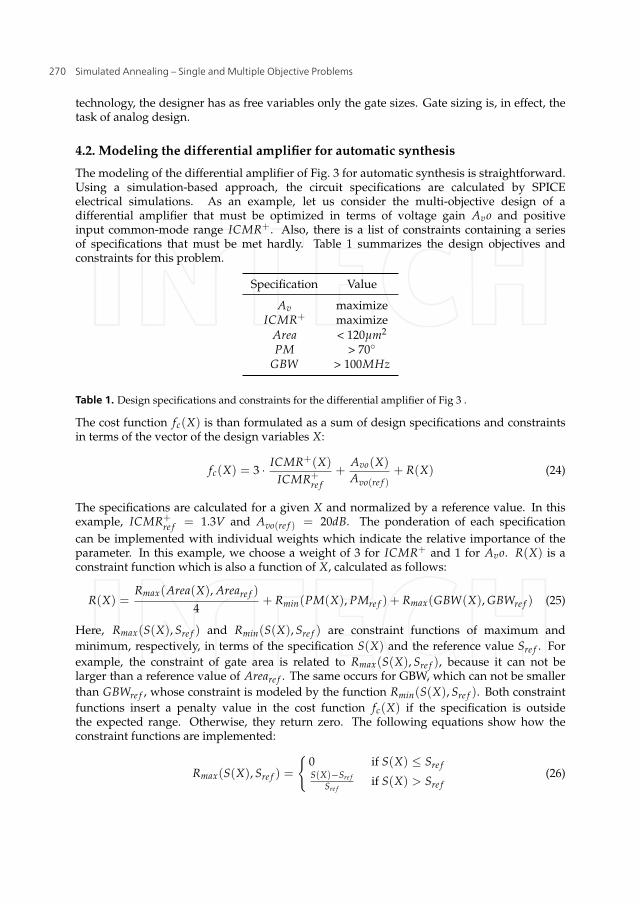
The modeling of the differential amplifier of Fig. 3 for automatic synthesis is straightforward.Using a simulation-based approach, the circuit specifications are calculated by SPICEelectrical simulations. As an example, let us consider the multi-objective design of adifferential amplifier that must be optimized in terms of voltage gain Avo and positiveinput common-mode range ICMR+. Also, there is a list of constraints containing a seriesof specifications that must be met hardly. Table 1 summarizes the design objectives andconstraints for this problem.
Specification Value
Av maximizeICMR+ maximize
Area < 120μm2
PM > 70◦GBW > 100MHz
Table 1. Design specifications and constraints for the differential amplifier of Fig 3 .
The cost function fc(X) is than formulated as a sum of design specifications and constraintsin terms of the vector of the design variables X:
fc(X) = 3 · ICMR+(X)
ICMR+re f
+Avo(X)
Avo(re f )+ R(X) (24)
The specifications are calculated for a given X and normalized by a reference value. In thisexample, ICMR+
re f = 1.3V and Avo(re f ) = 20dB. The ponderation of each specificationcan be implemented with individual weights which indicate the relative importance of theparameter. In this example, we choose a weight of 3 for ICMR+ and 1 for Avo. R(X) is aconstraint function which is also a function of X, calculated as follows:
R(X) =Rmax(Area(X), Areare f )
4+ Rmin(PM(X), PMre f ) + Rmax(GBW(X), GBWre f ) (25)
Here, Rmax(S(X), Sre f ) and Rmin(S(X), Sre f ) are constraint functions of maximum andminimum, respectively, in terms of the specification S(X) and the reference value Sre f . Forexample, the constraint of gate area is related to Rmax(S(X), Sre f ), because it can not belarger than a reference value of Areare f . The same occurs for GBW, which can not be smallerthan GBWre f , whose constraint is modeled by the function Rmin(S(X), Sre f ). Both constraintfunctions insert a penalty value in the cost function fc(X) if the specification is outsidethe expected range. Otherwise, they return zero. The following equations show how theconstraint functions are implemented:
Rmax(S(X), Sre f ) =
{0 if S(X) ≤ Sre fS(X)−Sre f
Sre fif S(X) > Sre f
(26)
270 Simulated Annealing – Single and Multiple Objective Problems

Simulated Annealing to Improve Analog Integrated Circuit Design: Trade-Offs and Implementation Issues 11
Rmin(S(X), Sre f ) =
{0 if S(X) ≥ Sre fS(X)−Sre f
Sre fif S(X) < Sre f
(27)
We used in this example the constraint reference values shown in Tab. 1 . In order to simplifythe analysis, we consider that all transistors of the circuit are of the same size. It is not apractical approach, since transistor M1 must be equal to M2, but not necessarily equal to M3and M4. However, this simplification allows the 2-D visualization of the problem and can beused to explain design trade-offs and automatic optimal search, providing an intuitive notionof the problem. So, we will consider in this analysis two free variables: L = L1 = L2 = L3 =L4 and W = W1 = W2 = W3 = W4. In this case, X = [W L].
The design space for Eq. 24 was fully mapped by electrical simulation varying W and L from1μm to 100μm with a step of 1μm. The target technology node was 0.35μm 3.3V CMOS. Fig.5 shows the plotted design space as a function of W and L. It is possible to note the highlynon-linear nature of the generated function and the existence of a valley in which is localizeda minimum value. The optimal solution for this sizing problem, i.e., the minimum value ofthe design space, is known exactly in this case and is located at W = 8μm and L = 20μm, withthe value of −1.9623.
0
20
40
60
80
100
0
20
40
60
80
100−2
−1.5
−1
−0.5
0
0.5
1
1.5
2
2.5
3
W (um)
Differential Amplifier − cost function
L (um)
Figure 5. Two-variables design space for a differential amplifier. The minimum is at W = 8μm andL = 20μm, with the value of −1.9623.
271Simulated Annealing to Improve Analog Integrated Circuit Design: Trade-Off s and Implementation Issues

12 Will-be-set-by-IN-TECH
4.3. Optimization of a differential amplifier
For the analysis of Simulated Annealing options and the influence over the automatic sizingprocedure of analog basic blocks, we will explore different configurations of temperatureschedule, state generation function and reannealing for global optimization and further localoptimization. Due to the random nature of some parameters of SA, an statistic analysis isneeded to understand the search behavior. We performed 1000 optimization runs for eachtemperature schedule function described before: Boltzman, Exponential and Fast. The stategeneration function was kept fixed as gBoltz(X) (Eq. 2). Each execution started with a differentseed for the random number generator function. The same parameters were used for the threefunctions, including the same random number vector for a fair comparison. A MATLAB scriptwas implemented and the native SA method (simulannealbnd) was used as the main boundconstrained optimization function.
4.3.1. Global optimization
Table 2 shows the mean of the optimal cost function found after 1000 executions of theoptimization procedure for each temperature schedule function. The Boltzman scheduleachieved the best values, with a mean final cost f ∗c of −1.960306, right near the optimalglobal solution of −1.9623. It means that most of the solutions provided by the procedurewith Boltzman are near the global optimum. Exponential and Fast temperature schedulesdemonstrate worst results in terms of cost. Boltzman result was obtained at expense of ahigher execution time and total number of iterators.
Temperature schedule f ∗c Execution time (s) Iterations
Boltzman -1.960306 16.32 1777.44Exponential -1.834720 9.57 1043.89
Fast -1.579269 12.99 1416.36
Table 2. Mean values of differential amplifier global optimization procedure for different temperatureschedule functions after 1000 executions.
The free variables W and L found by the three temperature schedule functions are shown inTab. 3. Again, Boltzman demonstrates the best results, with the mean values near the optimalsolution. Fast schedule presents the worst results in this configuration.
Temperature schedule W (μm) L (μm)
Boltzman 8.07 20.57Exponential 11.47 23.00
Fast 34.46 26.32
Optimum value 8.00 20.00
Table 3. Mean W and L values achieved by global optimization procedure of the differential amplifierafter 1000 runs for each different temperature schedule function.
272 Simulated Annealing – Single and Multiple Objective Problems

Simulated Annealing to Improve Analog Integrated Circuit Design: Trade-Offs and Implementation Issues 13
Fig. 6 shows a graph comparing the 3 temperature schedules, considering only the optimumsolutions obtained in relation to the optimization time. It is possible to notice the veryattractive results for Boltzman, which achieved 400 optimum solutions (over a set of 1000executions) in about 25 seconds of execution time. After this time, the number of optimalsolutions does not grow considerably, saturating in 430 at 37 seconds. The same saturationbehavior happens with Exponential and Fast temperature schedules, but with a very lowernumber of optimal solutions and at early execution time.
0 5 10 15 20 25 30 35 400
50
100
150
200
250
300
350
400
450
Time (s)
Opt
imal
Res
ults
Optimal Results versus Execution Time
TBoltz
TExp
TFast
Figure 6. Optimal results versus execution time for the global optimization of a differential amplifier,considering 3 different temperature schedule functions.
4.3.2. Global followed by local optimization
In order to improve the results obtained by global optimization with Simulated Annealing, weapply a local optimization algorithm over the previous set of solutions generated by SA withthe three temperature schedule functions. We choose the interior point algorithm [18], whichis suitable for linear and non-linear convex design spaces. We suppose that the design spaceregion near the solution provided by the global optimization and evolving the global optimumsolution is convex and can be explored by this method. The algorithm was implemented byusing the MATLAB native function fmincon. The results can be seen in Tab. 4 . It is clear theimprovement obtained by the local optimization. The mean final cost of the 1000 executionsfor the three temperature schedules are close to the known global optimum of−1.960306. Thetotal execution time (including global followed by local execution times) was increased byabout 50%, but it is still in a reasonable value, near 20 seconds.
273Simulated Annealing to Improve Analog Integrated Circuit Design: Trade-Off s and Implementation Issues

14 Will-be-set-by-IN-TECH
Temperature schedule f ∗c Execution time (s)
Boltzman -1.961759 24.40Exponential -1.927647 18.51
Fast -1.786238 22.43
Table 4. Mean values of differential amplifier after local optimization over the results obtained by globaloptimization shown in Tab. 2.
The mean values found for the free variables after the local search are shown in Tab. 5 .Comparing to the previous values provided by the global optimization, it is possible tonote the great improvement of the Exponential temperature schedule, whose mean W andL approached very near to the global optimum.
Temperature schedule W (μm) L (μm)
Boltzman 8.07 19.99Exponential 9.68 20.30
Fast 20.12 21.59
Optimum value 8.00 20.00
Table 5. Mean W and L values achieved by local optimization procedure of the differential amplifierover the results obtained by global optimization shown in tab. 3.
0 5 10 15 20 25 30 35 40 45 500
100
200
300
400
500
600
700
800
900
Time (s)
Opt
imal
Res
ults
Optimal Results versus Execution Time
T
Boltz
TExp
TFast
TBoltz
+ Local
TExp
+ Local
TFast
+ Local
Figure 7. Optimal results versus execution time for the global optimization of a differential amplifier,considering 3 different temperature schedule functions - global and local.
274 Simulated Annealing – Single and Multiple Objective Problems
Simulated Annealing to Improve Analog Integrated Circuit Design: Trade-Offs and Implementation Issues 15
In terms of the number of optimal solutions found over the 1000 executions, the local searchalso demonstrate an improvement. Fig. 7 shows the results obtained, in which we can seethat, for Boltzman schedule, almost 90% of the final solutions are optimal, an improvementof more than 50% over the global optimization. The same occurs for the other temperatureschedules.
We can observe the improvement in the number of optimal solutions with local search in Fig. 8,which presents the frequency histogram of the resulting final cost provided by global search(Fig. 8(a)) and global search followed by local search (Fig. 8(b)) for the 3 different temperatureschedules. Besides the increase in the number of optimal solutions found, the inclusion oflocal search after global search also approximated the remaining non-optimal solutions in thedirection to the best known value.
4.3.3. Global optimization with reannealing
For the analysis of the influence of reannealing in the optimization process, we performedsome experiments executing Simulated Annealing with reannealing intervals of 200, 450,700 and 950 iterations. Again, 1000 executions were done in order to guarantee a statisticalanalysis for the three temperature schedule functions described before.
Fig. 9 shows the relation between the number of optimal solutions found by Boltzmanschedule function versus the execution time for reannealing intervals from 200 to infinite (i.e.,no reannealing). Reannealing interval affects the number of optimal solutions in this case. Asthe interval decrease, the number of optimal solutions decrease too. The best configuration iswith no reannealing, demonstrating that it is not interesting to use reannealing with TBoltz. Ithappens because the temperature decreases slowly at the beginning of the annealing process.With the reannealing, the temperature increases for higher values before the search in thedesign space reaches a path trending to the optimal solution.
When the temperature schedule function is modified to Exponential, the behavior is opposite.As the reannealing interval decreases, more optimal solutions are found. Fig. 10 shows therelation between optimal solutions found and execution time for this temperature scheduleconfiguration.
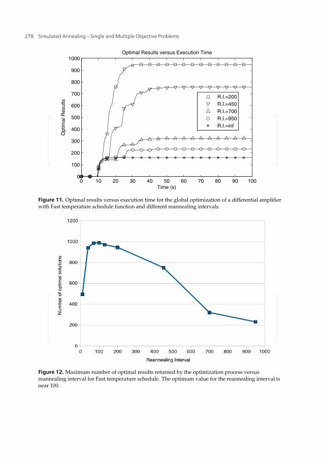
The same occurs for the Fast temperature schedule function, shown in Fig. 11. As thereannealing interval diminishes, the number of optimal solutions increases. This behavior ismaintained for ever small intervals. A high improvement in the number of optimal solutionsis obtained for reannealing intervals in the order of 100 iterations, as shown in Fig. 12. Asthe temperature decreases very fast, the reannealing allows to avoid local minima. Thus,it increases the chances of finding the correct path to the optimum solution. Also, we canobserve the existence of an optimum value for the reannealing interval which returns themaximum number of optimal solutions.
4.3.4. Analysis of state generation function
The variation of the state generation function is also a factor that can change the convergenceof the Simulated Annealing algorithm. Two of these functions are analyzed here: Boltzmanand Fast. The combinations of temperature schedule function and state generation functionproduce distinct results for the synthesis of the differential amplifier. Fig. 13 shows
275Simulated Annealing to Improve Analog Integrated Circuit Design: Trade-Off s and Implementation Issues

16 Will-be-set-by-IN-TECH
−1.96 −1.95 −1.94 −1.930
100
200
300
400
500
600
700
800
900
1000
TBoltz
Cost Function (fc)
Fre
quen
cy
−2 −1.8 −1.6 −1.4 −1.20
100
200
300
400
500
600
700
800
900
1000
TExp
Cost Function (fc)
Fre
quen
cy
−2 −1.5 −10
100
200
300
400
500
600
700
800
900
1000
TFast
Cost Function (Fc)
Fre
quen
cy
(a) Global search with Simulated Annealing.
−1.96 −1.95 −1.94 −1.930
100
200
300
400
500
600
700
800
900
1000
TBoltz
+ Local
Cost Function (fc)
Fre
quen
cy
−2 −1.8 −1.6 −1.4 −1.20
100
200
300
400
500
600
700
800
900
1000
TExp
+ Local
Cost Function (fc)
Fre
quen
cy
−2 −1.5 −10
100
200
300
400
500
600
700
800
900
1000
TFast
+ Local
Cost Function (fc)
Fre
quen
cy
(b) Global search with Simulated Annealing followed by local search with Interior Point Algorithm.
Figure 8. Frequency histograms of the final cost found by the optimization process for three differenttemperature schedule functions: Boltzman, Exponential and Fast. Obs.: x-scales are different in eachchart for better visualization purpose.
the number of optimal solutions returned by the algorithm after 1000 executions for 6combinations.
We can notice that there are a great improvement in the quality of the solutions using Boltzmantemperature schedule together with Boltzman state generation function. This is the bestcombination, according to that was theoretical predicted in Section 2.
276 Simulated Annealing – Single and Multiple Objective Problems

Simulated Annealing to Improve Analog Integrated Circuit Design: Trade-Offs and Implementation Issues 17
0 10 20 30 40 50 60 70 80 90 1000
50
100
150
200
250
300
350
400
450
Time (s)
Opt
imal
Res
ults
Optimal Results versus Execution Time
R.I.=200R.I.=450R.I.=700R.I.=950R.I.=inf
Figure 9. Optimal results versus execution time for the global optimization of a differential amplifierwith Boltzman temperature schedule function and different reannealing intervals.
0 20 40 60 80 1000
50
100
150
200
250
300
350
Time (s)
Opt
imal
Res
ults
Optimal Results versus Execution Time
R.I.=200R.I.=450R.I.=700R.I.=950R.I.=inf
Figure 10. Optimal results versus execution time for the global optimization of a differential amplifierwith Exponential temperature schedule function and different reannealing intervals.
277Simulated Annealing to Improve Analog Integrated Circuit Design: Trade-Off s and Implementation Issues
18 Will-be-set-by-IN-TECH
0 10 20 30 40 50 60 70 80 90 1000
100
200
300
400
500
600
700
800
900
1000
Time (s)
Opt
imal
Res
ults
Optimal Results versus Execution Time
R.I.=200R.I.=450R.I.=700R.I.=950R.I.=inf
Figure 11. Optimal results versus execution time for the global optimization of a differential amplifierwith Fast temperature schedule function and different reannealing intervals.
Figure 12. Maximum number of optimal results returned by the optimization process versusreannealing interval for Fast temperature schedule. The optimum value for the reannealing interval isnear 100.
278 Simulated Annealing – Single and Multiple Objective Problems

Simulated Annealing to Improve Analog Integrated Circuit Design: Trade-Offs and Implementation Issues 19
0 5 10 15 20 25 30 35 400
100
200
300
400
500
600
700
800
900
1000
Time(s)
Opt
imal
Res
ults
Optimal Results versus Execution Time
T
Boltz − G
Fast
TExp
− GFast
TFast
− GFast
TBoltz
− GBoltz
TExp
− GBoltz
TFast
− GBoltz
Figure 13. Number of optimal results returned by the optimization process for the differential amplifierfor different annealing functions and temperature function schedules.
4.3.5. Analysis of best SA options for the differential amplifier
Results presented before allow us to suppose that the temperature schedule function affectsdirectly the quality of the solutions generated by the global optimization algorithm. TheBoltzman schedule, followed by a post-processing with a local search algorithm, demonstratebest convergence to the optimal point, at the expenses of a larger execution time. Thisadditional time, however, is not a problem if we consider that the chances of finding theoptimal (or near the optimal) solution are increased. For our 2-variables problem, thisadditional time is irrelevant (about 10s for 1000 executions). For more complex circuits withdozens of variables, the execution time can be a factor of concern. It is increased exponentiallywith the number of free variables, since the design space grows fast with the number of freevariables. We can estimate the design space size Ds(X) as:
Ds(X) = ∏i
xi(ub) − xi(lb)
xi(step)(28)
where xi(ub) and xi(lb) are upper an lower bounds of variable xi, respectively, and xi(step) isthe minimum step allowed for variable xi. It is clear that the exploration of the entire designspace is hard for a problem with several free variables. An alternative, in this case, is to usethe Fast temperature schedule with reannealing, which is also efficient in the design spaceexploration. Both Boltzman followed by local search and Fast with reannealing achieved theoptimal solution in about 90% of the cases. These configurations are candidates to be testedin a larger circuit.
279Simulated Annealing to Improve Analog Integrated Circuit Design: Trade-Off s and Implementation Issues

20 Will-be-set-by-IN-TECH
5. Operational amplifier designIn order to apply simulated annealing in a more realistic and practical operational amplifier,we syntesized a folded cascode in CMOS IBM 0.18μm, regular Vt, 1.8V technology node. Theschematics of this amplifier is shown in Fig. 14.
ib
ibM1 M2
M4
M5 M6
M7 M8
M9 M10
M11 M12Mbn
Mbp
VSS
VDD
W1, L1 W1, L1
W4, L4W4, L4 W11, L11 W11, L11
W9, L9 W9, L9
W7, L7 W7, L7
W5, L5 W5, L5
vbpc
vbncVin+ Vin−
Vout
Figure 14. Schematics of a CMOS folded cascode amplifier.
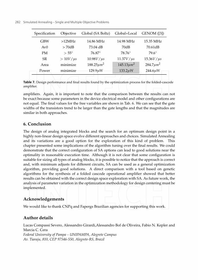
The modeling of this circuit for the proposed optimization process is simple and similar to theprevious described modeling of the differential amplifier. The SPICE netlist and the testbenchare the information necessary to describe the circuit and bias. The specifications are simulatedby an external electrical simulator (HSpice), which returns, for a given set of variables, theelectrical characteristics of the circuit. In our design there are 15 free variables, summarized inTab. 6. It leads to a very large 15-dimensional design space, which is difficult to explore andfind the minimum cost value. It is possible to limit the design space inserting constraints in thecost function related to the operation region of each transistor, forcing the devices to operateat saturation (VDS > VGS − VT) and strong inversion (VGS > VT) regions. The specificationsand design goals for this circuit are shown in Tab. 7. In the output is connected a capacitiveload of 3pF. We expect to size the circuit optimizing gate area and power dissipation whilemaintaining the constraints of GBW, low-voltage gain, phase margin and slew rate inside agiven range.
Using Boltzman for both temperature schedule function and state generation function,followed by local search with interior point algorithm, we find the final results shown inthe third and fourth columns of Tab. 7 for global and global followed by local searches,respectively. It is possible to note that all design objectives were reached, while keeping alldevices in the specified operation region. There is an improvement in the multi-objectivedesign goal with the post-processing local search. The final gate area is 145.13μm2 and
280 Simulated Annealing – Single and Multiple Objective Problems

Simulated Annealing to Improve Analog Integrated Circuit Design: Trade-Offs and Implementation Issues 21
Variable Final values (our work) Final values - GENOM ([3])
W1 11.58 μm 14.91 μm
W4 22.39 μm 6.99 μm
W5 14.13 μm 36.78 μm
W7 30.72 μm 63.04 μm
W9 7.16 μm 31.45 μm
W11 6.58 μm 7.32 μm
L1 0.73 μm 1.38 μm
L4 0.71 μm 1.94 μm
L5 0.29 μm 0.37 μm
L7 0.52 μm 0.91 μm
L9 0.87 μm 0.89 μm
L11 4.54 μm 2.19 μm
vbnc 0.0579 V 0.001 V
vbpc -0.0408 V -0,0449 V
ib 36.78 μA 48.51 μA
Table 6. Free variables and final results found for the folded-cascode amplifier optimization.
dissipated power is 133.2μW. The advantages of this approach is that the resulting circuit isalready validated by electrical simulations and does not need to be verified in another designstage.
We can make a direct comparison of the results obtained by this work using SA with otherapproaches, such as the tools that use genetic algorithms as main optimization heuristic.Although it is difficult to perform a fair comparison with other works in the literature,mainly because the experimental setup in general can not be reproduced with the providedinformation and there is no standard benchmarks in analog design automation, it is stillinteresting to compare the general performance of our methodology with other results oversimilar circuits and design objectives.
In this sense, the results presented by [3] with the GENOM tool are passible to comparison,because the same experimental setup can be reproduced - although some implementationdetails are not available, such as the parameters of the electrical model. This tool is based ona variation of genetic algorithm as the main optimization heuristic. The folded cascode wasimplemented in UMC 0.18μm technology. The final results obtained by GENOM for the samecircuit synthesized by our approach are summarized in the fiftieth column of Tab. 7.
We can see that both methodologies present similar results for the design constraints. By theother side, both power dissipation and gate area depicted by our approach using SimulatedAnnealing are about half the final values provided by GENOM. Power dissipation wasdecreased in 45.5% and gate area in 49%, a great improvement in circuit performance. Theseresults prove that SA is a powerful heuristic for the design of micro-power operational
281Simulated Annealing to Improve Analog Integrated Circuit Design: Trade-Off s and Implementation Issues
22 Will-be-set-by-IN-TECH
Specification Objective Global (SA Boltz) Global+Local GENOM ([3])
GBW >12MHz 14.86 MHz 14.98 MHz 15.35 MHz
Av0 > 70dB 73.04 dB 70dB 70.61dB
PM > 55◦ 76.87◦ 78.76◦ 79.6◦
SR > 10V/μs 10.98V/μs 11.37V/μs 15.36V/μs
Area minimize 188.25μm2 145.13μm2 284.7μm2
Power minimize 129.9μW 133.2μW 244.6μW
Table 7. Design performance and final results found by the optimization process for the folded-cascodeamplifier.
amplifiers. Again, it is important to note that the comparison between the results can notbe exact because some parameters in the device electrical model and other configurations arenot equal. The final values for the free variables are shown in Tab. 6. We can see that the gatewidths of the transistors trend to be larger than the gate lengths and that the magnitudes aresimilar in both approaches.
6. Conclusion
The design of analog integrated blocks and the search for an optimum design point in ahighly non-linear design space evolve different approaches and choices. Simulated Annealingand its variations are a good option for the exploration of this kind of problem. Thischapter presented some implications of the algorithm tuning over the final results. We coulddemonstrate that the correct configuration of SA options can lead to good solutions near theoptimality in reasonable execution time. Although it is not clear that some configuration issuitable for sizing all types of analog blocks, it is possible to notice that the approach is correctand, with minimum adjusts for different circuits, SA can be used as a general optimizationalgorithm, providing good solutions. A direct comparison with a tool based on geneticalgorithms for the synthesis of a folded cascode operational amplifier showed that betterresults can be obtained with the correct design space exploration with SA. As future work, theanalysis of parameter variation in the optimization methodology for design centering must beimplemented.
Acknowledgements
We would like to thank CNPq and Fapergs Brazilian agencies for supporting this work.
Author details
Lucas Compassi Severo, Alessandro Girardi,Alessandro Bof de Oliveira, Fabio N. Kepler andMarcia C. CeraFederal University of Pampa – UNIPAMPA, Alegrete CampusAv. Tiaraju, 810, CEP 97546-550, Alegrete-RS, Brazil
282 Simulated Annealing – Single and Multiple Objective Problems

Simulated Annealing to Improve Analog Integrated Circuit Design: Trade-Offs and Implementation Issues 23
7. References
[1] Aguiar, H., Junior, O., Ingber, L., Petraglia, A., Petraglia, M. R. & Machado, M. A. S.[2012]. Adaptive Simulated Annealing, Vol. 35 of Intelligent Systems Reference Library,Springer, pp. 33–62.
[2] Allen, P. E. & Holberg, D. R. [2011]. CMOS Analog Circuit Design, The Oxford Series inElectrical and Computer Engineering, 3rd edn, Oxford.
[3] Barros, M., Guilherme, J. & Horta, N. [2010]. Analog Circuits and Systems Optimizationbased on Evolutionary Computation Techniques, Vol. 294 of Studies in ComputationalIntelligence, 1st edn, Springer.
[4] Degrauwe, M., Nys, ., Dukstra, E., Rijmenants, J., Bitz, S., Gofart, B. L. A. G., Vitoz,E. A., Cserveny, S., Meixenberger, C., Stappen, G. V. & Oguey, H. J. [1987]. Idac:An interactive design tool for analog cmos circuits, IEEE Journal of Solid-State CircuitsSC-22(6): 1106–1116.
[5] der Plas, G. V., Gielen, G. & Sansen, W. M. C. [2002]. A Computer-Aided Design andSynthesis Environment for Analog Integrated Circuits, Vol. 672 of The Springer InternationalSeries in Engineering and Computer Science, Springer.
[6] El-Turky, F. M. & Perry, E. E. [1989]. BLADES: an artificial intelligence approach to analogcircuit design, IEEE Trans. on CAD of Integrated Circuits and Systems 8(6): 680–692.URL: http://doi.ieeecomputersociety.org/10.1109/43.31523
[7] Geman, S. & Geman, D. [1984]. Stochastic relaxation, gibbs distributions, and thebayesian restoration of images, IEEE Transactions on Pattern Analysis and MachineIntelligence PAMI-6(6): 721–741.
[8] Girardi, A. & Bampi, S. [2003]. LIT - an automatic layout generation tool for trapezoidalassociation of transistors for basic analog building blocks, DATE, IEEE Computer Society,pp. 11106–11107.URL: http://doi.ieeecomputersociety.org/10.1109/DATE.2003.10028
[9] Girardi, A. & Bampi, S. [2007]. Power constrained design optimization of analog circuitsbased on physical gm/id characteristics, Journal of Integrated Circuits and Systems 2: 22=28.
[10] Glelen, G., Walscharts, H. & Sansen, W. [1989]. Isaac: A symbolic simulator for analogcircuits, IEEE Journal of Solid-State Circuits 24(6): 1587–1597.
[11] Harjani, R., Rutenbar, R. A. & Carley, L. R. [1989]. OASYS: a framework for analog circuitsynthesis, IEEE Trans. on CAD of Integrated Circuits and Systems 8(12): 1247–1266.URL: http://doi.ieeecomputersociety.org/10.1109/43.44506
[12] Hershenson, M., Boyd, S. P. & Lee, T. H. [2001]. Optimal design of a CMOS op-amp viageometric programming, IEEE Transactions on Computer-Aided Design 20(1): 1–21.URL: http://www.stanford.edu/ boyd/opamp.html
[13] Ingber, L. [1996]. Adaptive simulated annealing (asa): Lessons learned, Control andCybernetics 25(1): 33 – 54.
[14] Ingber, L. [1989]. Very fast simulated re-annealing, Mathematical Computer Modelling12(8): 967 – 973.
[15] Liu, B., Fernandez, F. V., Gielen, G., Castro-Lopez, R. & Roca, E. [2009]. A memeticapproach to the automatic design of high-performance analog integrated circuits, ACMTransactions on Design Automation of Electronic Systems 14.
[16] Mandal, P. & Visvanathan, V. [2001]. CMOS op-amp sizing using a geometricprogramming formulation, IEEE Trans. on CAD of Integrated Circuits and Systems20(1): 22–38.URL: http://doi.ieeecomputersociety.org/10.1109/43.905672
283Simulated Annealing to Improve Analog Integrated Circuit Design: Trade-Off s and Implementation Issues

24 Will-be-set-by-IN-TECH
[17] Nye, W., Riley, D. C., Sangiovanni-Vincentelli, A. L. & Tits, A. L. [1988]. DELIGHT.SPICE:an optimization-based system for the design of integrated circuits, IEEE Trans. on CAD ofIntegrated Circuits and Systems 7(4): 501–519.URL: http://doi.ieeecomputersociety.org/10.1109/43.3185
[18] Press, W., Teukolsky, S., Vetterling, W. & Flannery, B. [2007]. Numerical Recipes: The Artof Scientific Computing, 3rd edn, Cambridge University Press, New York, chapter Section10.11. Linear Programming: Interior-Point Methods.
[19] Razavi, B. [2000]. Design of Analog CMOS Integrated Circuits, 1st edn, McGraw-Hil.[20] Szu, H. & Hartley, R. [1987]. Fast simulated annealing, Physical Letters A 122: 157–162.[21] Vytyaz, I., Lee, D. C., Hanumolu, P. K., Moon, U.-K. & Mayaram, K. [2009]. Automated
design and optimization of low-noise oscillators, Transactions on Computer-Aided Designof Integrated Circuits and Systems 28(5): 609–622.
284 Simulated Annealing – Single and Multiple Objective Problems