˘ ˇ - ti.com · slvs216b − june 1999 − june 2008 ... c2+ 15 positive terminal of the...
TRANSCRIPT

SLVS216B − JUNE 1999 − JUNE 2008
1POST OFFICE BOX 655303 • DALLAS, TEXAS 75265
features
Up to 150-mA Output Current
Less Than 10-mV pp Output Voltage Ripple
No Inductors Required/Low EMI
Regulated 5-V ±4% Output
Only Four External Components Required
Up to 90% Efficiency
2.7-V to 5.4-V Input Voltage Range
60-µA Quiescent Supply Current
0.05-µA Shutdown Current
Load Isolated in Shutdown
Space-Saving Thermally-Enhanced TSSOPPowerPAD Package
Evaluation Module Available(TPS60110EVM−132)
applications
Replaces DC/DC Converters W ith Inductors in− Battery-Powered Applications− Li-Ion Battery to 5-V Conversion− Portable Instruments− Battery-Powered Microprocessor
Systems− Miniature Equipment− Backup-Battery Boost Converters− PDAs− Laptops− Handheld Instrumentation− Medical Instruments
description
The TPS60111 step-up, regulated charge pumpgenerates a 5-V ±4% output voltage from a 2.7-Vto 5.4-V input voltage (three alkaline, NiCd, orNiMH batteries; or, one lithium or lithium ionbattery). Output current is 150 mA from a 3-Vinput. Only four external capacitors are needed tobuild a complete low-noise dc/dc converter. Thepush-pull operating mode of two single-endedcharge pumps assures the low output voltageripple as current is continuously transferred to theoutput. From a 3-V input, the TPS60111 can startinto full load with loads as low as 33 Ω.
The TPS60111 features either constant frequencymode to minimize noise and output voltage rippleor the power-saving pulse-skip mode to extendbattery life at light loads. The TPS60111 switchingfrequency is 300 kHz. The logic shutdown functionreduces the supply current to 1-µA (max) anddisconnects the load from the input. Specialcurrent-control circuitry prevents excessive cur-rent from being drawn from the battery duringstart-up. This dc/dc converter requires noinductors and has low EMI. It is available in thesmall 20-pin TSSOP PowerPAD package(PWP).
Copyright 1999 − 2008, Texas Instruments Incorporated ! " #$%! " &$'(#! )!%*)$#!" # ! "&%##!" &% !+% !%" %," "!$%!""!)) -!.* )$#! &#%""/ )%" ! %#%""(. #($)%!%"!/ (( &%!%"*
Please be aware that an important notice concerning availability, standard warranty, and use in critical applications ofTexas Instruments semiconductor products and disclaimers thereto appears at the end of this data sheet.
PowerPAD is a trademark of Texas Instruments Incorporated.
output voltage ripple
typical operating circuit
Figure 1
SKIP =COM = CLK = 0 VVIN = 3.6 VIO = 150 mACO = 22 µF + 10 µF
X5R Ceramic
5.2
5
5.05
5.1
5.15
4.8
4.85
4.9
4.95
− O
utpu
t Vol
tage
− V
VO
52.50 0.5 1 1.5 2 3 3.5 4 4.5
t − Time − µs
ININ
C1+
C1−
ENABLE
OUTOUT
FB
C2+
C2−
SYNC
SKIP COM CLK
PGND GND
INPUT2.7 V to
5.4 V
CIN 4.7 µF
OUTPUT5 V150 mA
CO15 µF
C2F1 µF
C1F1 µF
+
OFF/ON
TPS60110+

SLVS216B − JUNE 1999 − JUNE 2008
2 POST OFFICE BOX 655303 • DALLAS, TEXAS 75265
1
2
3
4
5
6
78
9
10
20
19
18
17
16
15
1413
12
11
GNDSYNC
ENABLEFB
OUTC1+
INC1−
PGNDPGND
GNDCLKCOMSKIPOUTC2+INC2−PGNDPGND
PWP PACKAGE(TOP VIEW)
Figure 2. Bottom View of PWP Package,Showing the Thermal Pad
ThermalPad
AVAILABLE OPTIONS
PACKAGE
TSSOP†
(PWP)
TPS60111PWP† This package is available taped and reeled. To order this packaging
option, add an R suffix to the part number (e.g., TPS60111PWPR).
Terminal Functions
TERMINALI/O DESCRIPTION
NAME NO.I/O DESCRIPTION
CLK 19 I Input for external clock signal. If the internal clock is used, connect this terminal to GND.
C1+ 6 Positive terminal of the charge-pump capacitor C1F
C1− 8 Negative terminal of the charge-pump capacitor C1F
C2+ 15 Positive terminal of the charge-pump capacitor C2F
C2− 13 Negative terminal of the charge-pump capacitor C2F
COM 18 I Mode selection.When COM is logic low the charge pump operates in push-pull mode to minimize output ripple. When COM isconnected to IN the regulator operates in single-ended mode requiring only one flying capacitor.
ENABLE 3 I ENABLE Input. The device turns off, the output disconnects from the input, and the supply current decreases to0.05 µA when ENABLE is a logic low. ENABLE high may only be applied when VIN is inside the recommendedoperating range.
FB 4 I FEEDBACK input. Connect FB to OUT as close to the load as possible to achieve best regulation. Resistive divideris on-chip to match internal reference voltage of 1.22 V.
GND 1, 20 GROUND. Analog ground for internal reference and control circuitry. Connect to PGND through a short trace.
IN 7, 14 I Supply Input. Connect to an input supply in the 2.7-V to 5.4-V range. Bypass IN to GND with a (CO/2) µF capacitor.Connect both INs through a short trace.
OUT 5, 16 O Regulated 5-V power output. Connect both OUTs through a short trace and bypass OUT to GND with the outputfilter capacitor CO.
PGND 9−12 PGND power ground. Charge-pump current flows through this pin. Connect all PGNDs together.
SKIP 17 I Mode selection. When SKIP is logic low the charge pump operates in constant-frequency mode. Thus output rippleand noise are minimized. When SKIP is connected to IN, the regulator operates in low-quiescent-currentpulse-skip mode.
SYNC 2 I Selection for external clock signal. Connect to GND to use the internally generated clock signal. Connect to INfor external synchronization. In this case, the clock signal needs to be fed through CLK.

SLVS216B − JUNE 1999 − JUNE 2008
3POST OFFICE BOX 655303 • DALLAS, TEXAS 75265
absolute maximum ratings (unless otherwise noted) †‡
Input voltage range, VI (IN, OUT, ENABLE, SKIP, COM, CLK, FB, SYNC) −0.3 V to 5.5 V. . . . . . . . . . . . . . . . Differential input voltage, VID (C1+, C2+ to GND) −0.3 V to (VO + 0.3 V). . . . . . . . . . . . . . . . . . . . . . . . . . . . . . Differential input voltage, VID (C1−, C2− to GND) −0.3 V to (VIN + 0.3 V). . . . . . . . . . . . . . . . . . . . . . . . . . . . . . Continuous total power dissipation See Dissipation Rating Tables. . . . . . . . . . . . . . . . . . . . . . . . . . . . . . . . . . . . Continuous output current 200 mA. . . . . . . . . . . . . . . . . . . . . . . . . . . . . . . . . . . . . . . . . . . . . . . . . . . . . . . . . . . . . . . . Storage temperature range, Tstg −55°C to 150°C. . . . . . . . . . . . . . . . . . . . . . . . . . . . . . . . . . . . . . . . . . . . . . . . . . . Lead temperature 1,6 mm (1/16 inch) from case for 10s 260°C. . . . . . . . . . . . . . . . . . . . . . . . . . . . . . . . . . . . . . . Maximum junction temperature, TJ 150°C. . . . . . . . . . . . . . . . . . . . . . . . . . . . . . . . . . . . . . . . . . . . . . . . . . . . . . . . .
† Stresses beyond those listed under “absolute maximum ratings” may cause permanent damage to the device. These are stress ratings only, andfunctional operation of the device at these or any other conditions beyond those indicated under “recommended operating conditions” is notimplied. Exposure to absolute-maximum-rated conditions for extended periods may affect device reliability.
‡ VENABLE, VSKIP, VCOM, VCLK and VSYNC can exceed VIN up to the maximum rated voltage without increasing the leakage currentdrawn by these mode select inputs.
DISSIPATION RATING TABLE 1 − FREE-AIR TEMPERATURE (see Figure 3)
PACKAGETA ≤ 25°C DERATING FACTOR TA = 70°C TA = 85°C
PACKAGETA ≤ 25 C
POWER RATINGDERATING FACTORABOVE TA = 25°C
TA = 70 CPOWER RATING
TA = 85 CPOWER RATING
PWP 700 mW 5.6 mW/°C 448 mW 364 mW
DISSIPATION RATING TABLE 2 − CASE TEMPERATURE (see Figure 4)
PACKAGETC ≤ 62.5°C DERATING FACTOR TC = 70°C TC = 85°C
PACKAGETC ≤ 62.5 C
POWER RATINGDERATING FACTORABOVE TC = 62.5°C
TC = 70 CPOWER RATING
TC = 85 CPOWER RATING
PWP 25 W 285.7 mW/°C 22.9 W 18.5 W
Figure 3
1200
800
400
025 50 75 100
− M
axim
um C
ontin
uous
Dis
sipa
tion
− m
W
DISSIPATION DERATING CURVE§
vsFREE-AIR TEMPERATURE
125 150
1400
1000
600
200
PWP PackageRθJA = 178°C/W
PD
TA − Free-Air Temperature − °C
Figure 4
MAXIMUM CONTINUOUS DISSIPATION§
vsCASE TEMPERATURE
TC − Case Temperature − °C
15
10
5
025 50 75 100
20
25
30
125 150
Measured with the exposed thermal padcoupled to an infinite heat sink with athermally conductive compound (thethermal conductivity of the compoundis 0.815 W/m ⋅ °C). The RθJC is 3.5°C/W.
PWP Package
− M
axim
um C
ontin
uous
Dis
sipa
tion
− W
PD
§ Dissipation rating tables and figures are provided for maintenance of junction temperature at or below absolute maximum temperature of 150°C.It is recommended not to exceed a junction temperature of 125°C.

SLVS216B − JUNE 1999 − JUNE 2008
4 POST OFFICE BOX 655303 • DALLAS, TEXAS 75265
electrical characteristics at C IN = 15 µF, C1F = C2F = 2.2 µF†, CO = 33 µF, TC = −40°C to 85°C, VIN = 3 V, VFB = VO, VENABLE = VIN, VSKIP = VIN or 0 V and V COM = VCLK = VSYNC = 0 V (unless otherwisenoted)
PARAMETER TEST CONDITIONS MIN TYP MAX UNIT
VIN Input voltage 2.7 5.4 V
IO(MAX) Maximum output current 150 mA
VO Output voltage
2.7 V < VIN < 3 V, 0 < IO < 75 mA,VO(Start-Up) = 5 V, TC = 25°C 4.8 5 5.2
VVO Output voltage3 V < VIN < 5 V, 0 < IO < 150 mA 4.8 5 5.2
V
5 V < VIN < 5.4 V, 0 < IO < 150 mA 4.8 5 5.25
VO(RIP) Output voltage ripple IO = 150 mA, VSKIP = 0 V 10‡ mVPP
IO(LEAK) Output leakage current VIN = 3.6 V, VENABLE = 0 V 1 µA
IQQuiescent current VSKIP = VIN = 3.6 V 60 90 µA
IQQuiescent current(no-load input current) VSKIP = 0 V, VIN = 3.6 V 2.8 mA
IDD(SDN) Shutdown supply current VIN = 3.6 V, VENABLE = 0 V 0.05 1 µA
fOSC(int) Internal switching frequency VIN = 3.6 V 200 300 400 kHz
fOSC(ext) External clock frequency VSYNC = VIN, VIN = 2.7 V to 5.4 V 400 600 800 kHz
External clock duty cycle VSYNC = VIN, VIN= 2.7V to 5.4 V 20% 80%
Efficiency IO = 75 mA 80%
VINLInput voltage low,ENABLE, SKIP, COM, CLK, SYNC
VIN = 2.7 V0.3 ×VIN
V
VINHInput voltage high,ENABLE, SKIP, COM, CLK, SYNC
VIN = 5.4 V0.7 ×VIN
V
II(LEAK)Input leakage current,ENABLE, SKIP, COM, CLK, SYNC
VENABLE = VSKIP = VCOM = VCLK =VSYNC = VGND or VIN
0.01 0.1 µA
Output load regulationVO = 5 V, 1 mA < IO < 150 mATC = 25°C 0.002 %/mA
Output line regulation3 V < VIN < 5 V, VO = 5 V,IO = 75 mA, TC = 25°C 0.6 %/V
Short circuit currentVIN = 3.6 V VO = 0 V,TC = 25°C 150 mA
† Use only ceramic capacitors with X5R or X7R dielectric as flying capacitors.‡ Achieved with CO = 22 µF + 10 µF X5R dielectric ceramic capacitor
SLVS216B − JUNE 1999 − JUNE 2008
5POST OFFICE BOX 655303 • DALLAS, TEXAS 75265
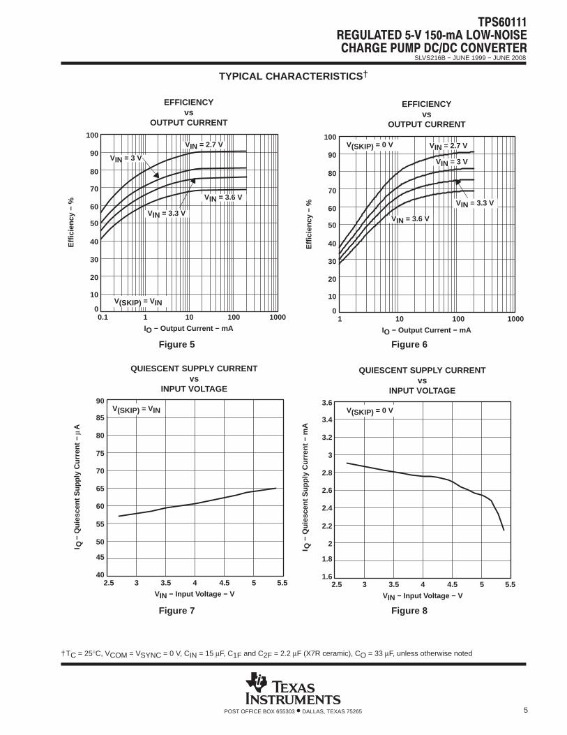
TYPICAL CHARACTERISTICS †
Figure 5
50
40
20
00.1 1 10
Effi
cien
cy −
%
70
90
EFFICIENCYvs
OUTPUT CURRENT100
100 1000
80
60
30
10
IO − Output Current − mA
V(SKIP) = VIN
VIN = 3 V
VIN = 3.3 V
VIN = 3.6 V
VIN = 2.7 V
Figure 6
50
40
20
01 10
Effi
cien
cy −
%
70
90
EFFICIENCYvs
OUTPUT CURRENT100
100 1000
80
60
30
10
IO − Output Current − mA
V(SKIP) = 0 V VIN = 2.7 V
VIN = 3 V
VIN = 3.3 V
VIN = 3.6 V
Figure 7
60
50
402.5 3 3.5 4
− Q
uies
cent
Sup
ply
Cur
rent
−
80
QUIESCENT SUPPLY CURRENTvs
INPUT VOLTAGE90
4.5 5.5
70
VIN − Input Voltage − V
I QA
µ
V(SKIP) = VIN
5
65
55
45
85
75
Figure 8
− Q
uies
cent
Sup
ply
Cur
rent
− m
A
QUIESCENT SUPPLY CURRENTvs
INPUT VOLTAGE
VIN − Input Voltage − V
I Q
2.5 3 3.5 4 4.5 5.55
V(SKIP) = 0 V
2.4
2
1.6
3.2
3.6
2.8
2.6
2.2
1.8
3.4
3
†TC = 25°C, VCOM = VSYNC = 0 V, CIN = 15 µF, C1F and C2F = 2.2 µF (X7R ceramic), CO = 33 µF, unless otherwise noted

SLVS216B − JUNE 1999 − JUNE 2008
6 POST OFFICE BOX 655303 • DALLAS, TEXAS 75265
TYPICAL CHARACTERISTICS †
Figure 9
IO − Output Current − mA
5
4.9
4.8
4.71 10
− O
utpu
t Vol
tage
− V
5.1
5.2
OUTPUT VOLTAGEvs
OUTPUT CURRENT5.3
100 1000
VO
V(SKIP) = 0 V
VIN = 4 V
VIN = 3.6 V
VIN = 3 V
VIN = 2.7 V
VIN = 5.4 V
Figure 10
IO − Output Current − mA
5
4.9
4.8
4.71 10
− O
utpu
t Vol
tage
− V
5.1
5.2
OUTPUT VOLTAGEvs
OUTPUT CURRENT5.3
100 1000
VO
V(SKIP) = VIN
VIN = 4 VVIN = 3.6 V
VIN = 3 V
VIN = 2.7 V
VIN = 5.4 V
Figure 11
5.04
4.98
4.94
4.9
− O
utpu
t Vol
tage
− V
5.06
5.08
OUTPUT VOLTAGEvs
INPUT VOLTAGE5.1
5.02
5
4.96
4.92
VIN − Input Voltage − V
VO
V(SKIP) = 0 V
2.5 3 3.5 4 4.5 5.55
IO = 1 mA to 10 mA
IO = 150 mA
Figure 12
5.04
4.98
4.94
4.9
− O
utpu
t Vol
tage
− V
5.06
5.08
OUTPUT VOLTAGEvs
INPUT VOLTAGE5.1
5.02
5
4.96
4.92
VIN − Input Voltage − V
VO
2.5 3 3.5 4 4.5 5.55
V(SKIP) = VINIO = 1 mA to 150 mA
†TC = 25°C, VCOM = VSYNC = 0 V, CIN = 15 µF, C1F and C2F = 2.2 µF (X7R ceramic), CO = 33 µF, unless otherwise noted

SLVS216B − JUNE 1999 − JUNE 2008
7POST OFFICE BOX 655303 • DALLAS, TEXAS 75265
TYPICAL CHARACTERISTICS †
Figure 13
5.03
5.02
5.010 2 4
5.04
OUTPUT VOLTAGEvs
TIME5.05
6 10
t − Time − µs
V(SKIP) = 0 VVIN = 3.6 VIO = 150 mACO = 22 µF + 10 µF X5R ceramic
ConstantFrequencyMode
− O
utpu
t Vol
tage
− V
VO
8
Figure 14
5.03
5.01
4.990 10 20 30
5.05
OUTPUT VOLTAGEvs
TIME5.07
40 50
t − Time − µs
V(SKIP) = VINVIN = 3.6 VIO = 150 mA
Pulse-Skip Mode
− O
utpu
t Vol
tage
− V
VO
Figure 15
5.01
200
100
00 2 4 6 8 10 12
− O
utpu
t Vol
tage
− V
5.02
5.04
t − Time − ms
LOAD TRANSIENT RESPONSE5.05
14 16 18 20
300
5.03
VO
− O
utpu
t Cur
rent
− m
AI O
V(SKIP) = 0 VIO = 10 mA to 150 mAVIN = 3.6 V
ConstantFrequencyMode
Figure 16
5
200
100
00 2 4 6 8 10 12
5.02
5.06
t − Time − ms
LOAD TRANSIENT RESPONSE
5.08
14 16 18 20
300
5.04
V(SKIP) = VIN = 3.6 VIO = 10 mA to 150 mA
Pulse-Skip Mode
− O
utpu
t Vol
tage
− V
VO
− O
utpu
t Cur
rent
− m
AI O
†TC = 25°C, VCOM = VSYNC = 0 V, CIN = 15 µF, C1F and C2F = 2.2 µF (X7R ceramic), CO = 33 µF, unless otherwise noted

SLVS216B − JUNE 1999 − JUNE 2008
8 POST OFFICE BOX 655303 • DALLAS, TEXAS 75265
TYPICAL CHARACTERISTICS †
Figure 17
5
4
3
20 1 2 3 4 5 6
− O
utpu
t Vol
tage
− V
5.02
5.06
t − Time − ms
LINE TRANSIENT RESPONSE5.08
7 8 9 10
5
5.04
VO
− In
put V
olta
ge −
VV
IN
V(SKIP) = 0 VIO = 150 mA
ConstantFrequencyMode
Figure 18
5
4
3
20 1 2 3 4 5 6
5.02
5.06
t − Time − ms
LINE TRANSIENT RESPONSE
5.08
7 8 9 10
5
5.04
V(SKIP) = VINIO = 150 mA
Pulse-Skip Mode
− O
utpu
t Vol
tage
− V
VO
− In
put V
olta
ge −
VV
IN
Figure 19
50
40
20
00 2.5 5
Out
put −
dB
60
80
f − Frequency − MHz
FREQUENCY SPECTRUMCONSTANT FREQUENCY MODE‡
90
7.5 10
70
30
10
Vµ
V(SKIP) = 0 VVIN = 3 VIO = 150 mARBW = 300 Hz
Figure 20
40
20
00 2.5 5
Out
put −
dB
60
100
f − Frequency − MHz
FREQUENCY SPECTRUMPULSE-SKIP MODE‡
7.5 10
Vµ
V(SKIP) = VINVIN = 3 VIO = 150 mARBW = 300 Hz80
†TC = 25°C, VCOM = VSYNC = 0 V, CIN = 15 µF, C1F and C2F = 2.2 µF (X7R ceramic), CO = 33 µF, unless otherwise noted‡Test circuit: TPS60110EVM−132 with TPS60111

SLVS216B − JUNE 1999 − JUNE 2008
9POST OFFICE BOX 655303 • DALLAS, TEXAS 75265
TYPICAL CHARACTERISTICS †
Figure 21
50
20
10
00 2.5 5
60
70
f − Frequency − MHz
FREQUENCY SPECTRUMCONSTANT FREQUENCY MODE‡
90
7.5 10
30
40
80
Out
put −
dB
Vµ
V(SKIP) = 0 VVIN = 3 VIO = 10 mARBW = 300 Hz
Figure 22
50
40
20
00 2.5 5
Out
put −
dB
60
80
f − Frequency − MHz
FREQUENCY SPECTRUMPULSE-SKIP MODE‡
90
7.5 10
70
30
10
Vµ
V(SKIP) = VINVIN = 3 VIO = 10 mARBW = 300 Hz
Figure 23
Skip = High
Skip = Low
50
30
20
02.5 3 3.5 4
Effi
cien
cy −
%
70
80
EFFICIENCYvs
INPUT VOLTAGE100
4.5 5.5
10
40
60
90
VIN − Input Voltage − V
5
IO = 150 mA
Figure 24
t − Time − µs
3
2
1
0
− O
utpu
t Vol
tage
− V 4
5
START-UP TIMING6
200
VO
R0 = 33.3 ΩVIN = 3 V
Enable
OUTPUT
−1400 1200
0
600 800 1000
†TC = 25°C, VCOM = VSYNC = 0 V, CIN = 15 µF, C1F and C2F = 2.2 µF (X7R ceramic), CO = 33 µF, unless otherwise noted‡Test circuit: TPS60110EVM−132 with TPS60111
SLVS216B − JUNE 1999 − JUNE 2008
10 POST OFFICE BOX 655303 • DALLAS, TEXAS 75265
detailed description
operating principle
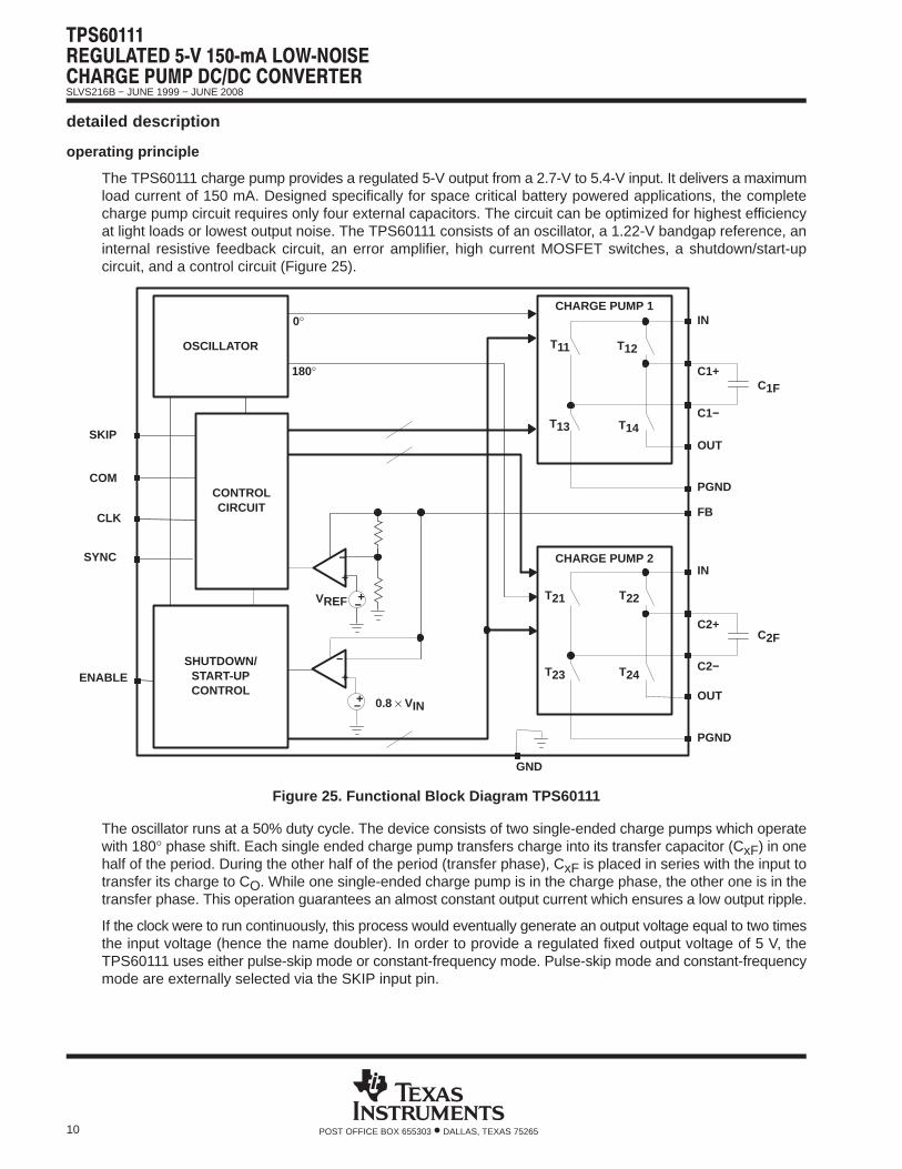
The TPS60111 charge pump provides a regulated 5-V output from a 2.7-V to 5.4-V input. It delivers a maximumload current of 150 mA. Designed specifically for space critical battery powered applications, the completecharge pump circuit requires only four external capacitors. The circuit can be optimized for highest efficiencyat light loads or lowest output noise. The TPS60111 consists of an oscillator, a 1.22-V bandgap reference, aninternal resistive feedback circuit, an error amplifier, high current MOSFET switches, a shutdown/start-upcircuit, and a control circuit (Figure 25).
C1+
C1−
ENABLE
OUT
FB
0°
180°
PGND
C1F
IN
CHARGE PUMP 2
C2+
C2−
OUT
PGND
C2F
IN
T22T21
OSCILLATOR
GND
SKIP
COM
CLK
VREF −+
−
+
CONTROLCIRCUIT
0.8 × VIN−+
−
+SHUTDOWN/
START-UPCONTROL
SYNC
T11 T12
T13 T14
T24T23
CHARGE PUMP 1
Figure 25. Functional Block Diagram TPS60111
The oscillator runs at a 50% duty cycle. The device consists of two single-ended charge pumps which operatewith 180° phase shift. Each single ended charge pump transfers charge into its transfer capacitor (CxF) in onehalf of the period. During the other half of the period (transfer phase), CxF is placed in series with the input totransfer its charge to CO. While one single-ended charge pump is in the charge phase, the other one is in thetransfer phase. This operation guarantees an almost constant output current which ensures a low output ripple.
If the clock were to run continuously, this process would eventually generate an output voltage equal to two timesthe input voltage (hence the name doubler). In order to provide a regulated fixed output voltage of 5 V, theTPS60111 uses either pulse-skip mode or constant-frequency mode. Pulse-skip mode and constant-frequencymode are externally selected via the SKIP input pin.

SLVS216B − JUNE 1999 − JUNE 2008
11POST OFFICE BOX 655303 • DALLAS, TEXAS 75265
detailed description (continued)
start-up procedure
During start-up, i.e. when ENABLE is set from logic low to logic high, the switches T12 and T14 (charge pump1), and the switches T22 and T24 (charge pump 2) are conducting to charge up the output capacitor until theoutput voltage VO reaches 0.8×VIN. When the start-up comparator detects this limit, the IC begins to operatein the mode selected with SKIP and COM. This start-up charging of the output capacitor guarantees a shortstart-up time and eliminates the need for a Schottky diode between IN and OUT.
pulse-skip mode
In pulse-skip mode (SKIP = high), the error amplifier disables switching of the power stages when it detects anoutput higher than 5 V. The oscillator halts. The IC then skips switching cycles until the output voltage dropsbelow 5 V. Then the error amplifier reactivates the oscillator and switching of the power stages starts again. Thepulse-skip regulation mode minimizes operating current because it does not switch continuously anddeactivates all functions except bandgap reference and error amplifier when the output is higher than 5 V. Whenswitching is disabled from the error amplifier, the load is also isolated from the input. SKIP is a logic input andshould not remain floating. The typical operating circuit of the TPS60111 in pulse skip mode is shown in Figure1.
constant-frequency mode
When SKIP is low, the charge pump runs continuously at the frequency fOSC. The control circuit, fed from theerror amplifier, controls the charge on C1F and C2F by driving the gates of the FETs T12/T13 and T22/T23,respectively. When the output voltage falls, the gate drive increases, resulting in a larger voltage across C1Fand C2F. This regulation scheme minimizes output ripple. Since the device switches continuously, the outputnoise contains well-defined frequency components, and the circuit requires smaller external capacitors for agiven output ripple. However, constant-frequency mode, due to higher operating current, is less efficient at lightloads than pulse-skip mode.
ININ
C1+
C1−
ENABLE
OUTOUT
FB
C2+
C2−
SYNC
SKIP COM CLK
PGND GND
INPUT2.7 V to 5.4 V
CIN 4.7 µF
OUTPUT5 V 150 mA
CO = 33 µF
C2F1 µF
C1F1 µF
+
OFF/ON
TPS60111+
Figure 26. Typical Operating Circuit TPS60111 in Constant Frequency Mode
Table 1. Tradeoffs Between Operating Modes
FEATURE PULSE-SKIP MODE(SKIP = High)
CONSTANT-FREQUENCY MODE(SKIP = Low)
Best light-load efficiency X
Smallest external component size for a given output ripple X
Output ripple amplitude Small amplitude Very small amplitude
Output ripple frequency Variable Constant
Load regulation Very good Good
NOTE: Even in pulse-skip mode the output ripple amplitude is small if the push-pull operating mode is selected via COM.

SLVS216B − JUNE 1999 − JUNE 2008
12 POST OFFICE BOX 655303 • DALLAS, TEXAS 75265
detailed description (continued)
push-pull operating mode
In push-pull operating mode (COM = low), the two single-ended charge pumps operate with 180° phase shift.The oscillator signal has a 50% duty cycle. Each single-ended charge pump transfers charge into its transfercapacitor (CxF) in one-half of the period. During the other half of the period (transfer phase), CxF is placed inseries with the input to transfer its charge to CO. While one single-ended charge pump is in the charge phase,the other one is in the transfer phase. This operation guarantees an almost constant output current whichensures a low output ripple. COM is a logic input and should not remain floating. The typical operating circuitof the TPS60111 in push-pull mode is shown in Figure 1 and Figure 26.
single-ended operating mode
When COM is high, the device runs in single-ended operating mode. The two single-ended charge pumpsoperate in parallel without phase shift. They transfer charge into the transfer capacitor (CF) in one half of theperiod. During the other half of the period (transfer phase), CF is placed in series with the input to transfer itscharge to CO. In single-ended operating mode only one transfer capacitor (CF = C1F + C2F) is required, resultingin less board space.
ININ
C1+
C1−
ENABLE
OUTOUT
FB
C2+
C2−
SYNC
SKIP COM CLK
PGND GND
INPUT2.7 V to 5.4 V
CIN 4.7 µF
OUTPUT5 V 150 mA
CO = 15 µF
CF = 2.2 µF
+
OFF/ON
TPS60111+
Figure 27. Typical Operating Circuit TPS60111 in Single-Ended Operating Mode
Table 2. Tradeoffs Between Operating Modes
FEATURE PUSH-PULL MODE(COM = Low)
SINGLE-ENDED MODE(COM = High)
Output ripple amplitude Small amplitude Large amplitude
Smallest board space X

SLVS216B − JUNE 1999 − JUNE 2008
13POST OFFICE BOX 655303 • DALLAS, TEXAS 75265
detailed description (continued)
shutdown
Driving ENABLE low places the device in shutdown mode. This disables all switches, the oscillator, and controllogic. The device typically draws 0.05-µA (1-µA max) of supply current in this mode. Leakage current drawn fromthe output is as low as 1 µA max. The device exits shutdown once ENABLE is set high level. The typical no-loadshutdown exit time is 20 µs. When the device is in shutdown, the load is isolated from the input and the outputis high impedance.
external clock signal
If the device operates at a user-defined frequency, an external clock signal can be used. Therefore, SYNC needsto be connected to IN and the external oscillator signal can drive CLK. The maximum external frequency islimited to 800 kHz. The switching frequency of the converter is half of the external oscillator frequency. It isrecommended to operate the charge pump in constant-frequency mode if an external clock signal is used sothat the output noise contains only well-defined frequency components.
ININ
C1+
C1−
ENABLE
OUTOUT
FB
C2+
C2−
SYNC
SKIP COM CLK
PGND GND
INPUT2.7 V to 5.4 V
CIN 4.7 µF
OUTPUT5 V 150 mA
CO = 33 µF
C2F1 µF
C1F1 µF
+
OFF/ON
TPS60111+
External Clock
Figure 28. Typical Operating Circuit TPS60111 With External Synchronization

SLVS216B − JUNE 1999 − JUNE 2008
14 POST OFFICE BOX 655303 • DALLAS, TEXAS 75265
APPLICATION INFORMATION
capacitor selection
The TPS60111 requires only four external capacitors as shown in the basic application circuit. Their values areclosely linked to the output current capacity, output noise requirements, and mode of operation. Generally, thetransfer capacitors (CxF) will be the smallest.
The input capacitor improves system efficiency by reducing the input impedance and stabilizes the input current.CIN is recommended to be about two to four times as large as CxF.
The output capacitor (CO) can be selected from 8-times to 50-times larger than CxF, depending on the modeof operation and ripple tolerance†. Tables 3 and 4 show capacitor values recommended for lowquiescent-current operation (pulse-skip mode) and for low output voltage ripple operation (constant-frequencymode). A recommendation is given for smallest size.
Table 3. Recommended Capacitor Values for Low Quiescent-Current Operation †(pulse-skip mode)
VIN [V]
IO [mA]
CIN[µF] CxF
[µF]
CO[µF]
OUTPUTVOLTAGE
RIPPLE VPPIN
[V]IO [mA]
TANTALUM CERAMIC
xF[µF]
TANTALUM CERAMICRIPPLE VPP
[mV]
3.6 75 4.7 1 15 150
3.6 75 4.7 (X7R) 1 10 (X5R) 105
3.6 150 4.7 1 15 150
3.6 150 4.7 (X7R) 1 10 (X5R) 105† All measurements are done with additional 1-µF X7R ceramic capacitors at input and output.
Table 4. Recommended Capacitor Values for Low Output Voltage Ripple Operation †(constant-frequency mode)
VIN [V]
IO[mA]
CIN[µF] CxF
[µF]
CO[µF]
OUTPUTVOLTAGE
RIPPLE VPPIN
[V]O
[mA]TANTALUM CERAMIC
xF[µF]
TANTALUM CERAMICRIPPLE VPP
[mV]
3.6 75 4.7 1 33 10
3.6 75 4.7 (X7R) 1 22 + 10, (X5R) 6
3.6 150 4.7 1 33 17
3.6 150 4.7 (X7R) 1 22 + 10, (X5R) 10† All measurements are done with additional 1-µF X7R ceramic capacitors at input and output.
† In constant-frequency mode always select CO ≥ 33 µF

SLVS216B − JUNE 1999 − JUNE 2008
15POST OFFICE BOX 655303 • DALLAS, TEXAS 75265
APPLICATION INFORMATION
For the TPS60111, the smallest board space size can be achieved using Sprague’s 595D-series tantalumcapacitors for input and output. However, with the trend towards high capacitance ceramic capacitors in smallersize packages, these type of capacitors might soon become competitive in size.
Table 5. Recommended Capacitors
MANUFACTURER PART NUMBER CAPACITANCE TYPE
Taiyo Yuden LMK212BJ105KG−TLMK212BJ225MG−TLMK316BJ475KL−TJMK316BJ106ML−TLMK432BJ226MM−T
1 µF2.2 µF4.7 µF10 µF22 µF
CeramicCeramicCeramicCeramicCeramic
AVX 0805ZC105KAT2A1206ZC225KAT2A
TPSC475K035R0600TPSC156K020R0450TPSC336K010R0375
1 µF2.2 µF4.7 µF15 µF33 µF
CeramicCeramicTantalumTantalumTantalum
Sprague 595D475X0016A2T595D156X06R3A2T595D156X0016B2T595D336X06R3A2T595D336X0016B2T595D336X0016C2T
4.7 µF15 µF15 µF33 µF33 µF33 µF
TantalumTantalumTantalumTantalumTantalumTantalum
Kemet T494B475M010AST494C156K010AST494C336K010AS
4.7 µF15 µF33 µF
TantalumTantalumTantalum
Table 6 lists the manufacturers of recommended capacitors. In most applications surface-mount tantalumcapacitors will be the right choice. However, ceramic capacitors will provide the lowest output voltage ripple dueto their typically lower ESR.
Table 6. Recommended Capacitor Manufacturers
MANUFACTURER CAPACITOR TYPE INTERNET
Taiyo Yuden X7R/X5R ceramic www.t−yuden.com
AVX X7R/X5R ceramicTPS−series tantalum
www.avxcorp.com
Sprague 595D−series tantalum593D−series tantalum
www.vishay.com
Kemet T494−series tantalum www.kemet.com
power dissipation
The power dissipated in the TPS60111 depends on output current and is approximated by:
PDISS IO 2 VIN VO for IQ IO
PDISS must be less than that allowed by the package rating. See the ratings for 20-PowerPAD packagepower-dissipation limits and deratings.
SLVS216B − JUNE 1999 − JUNE 2008
16 POST OFFICE BOX 655303 • DALLAS, TEXAS 75265
APPLICATION INFORMATION
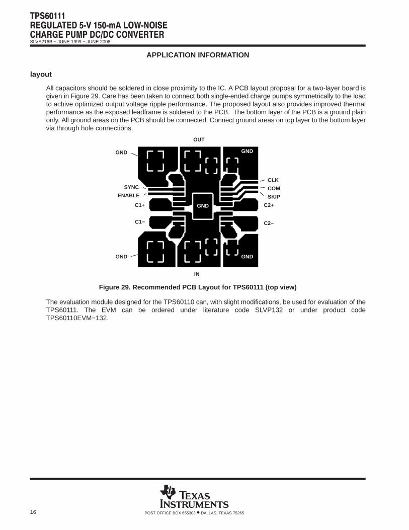
layout
All capacitors should be soldered in close proximity to the IC. A PCB layout proposal for a two-layer board isgiven in Figure 29. Care has been taken to connect both single-ended charge pumps symmetrically to the loadto achive optimized output voltage ripple performance. The proposed layout also provides improved thermalperformance as the exposed leadframe is soldered to the PCB. The bottom layer of the PCB is a ground plainonly. All ground areas on the PCB should be connected. Connect ground areas on top layer to the bottom layervia through hole connections.
GND
GND
GND
ENABLE
SYNC
C1+
C1−
GND
GND
OUT
IN
CLK
COM
SKIP
C2+
C2−
Figure 29. Recommended PCB Layout for TPS60111 (top view)
The evaluation module designed for the TPS60110 can, with slight modifications, be used for evaluation of theTPS60111. The EVM can be ordered under literature code SLVP132 or under product codeTPS60110EVM−132.

SLVS216B − JUNE 1999 − JUNE 2008
17POST OFFICE BOX 655303 • DALLAS, TEXAS 75265
APPLICATION INFORMATION
applications proposals
TPS60111 with LC output filter for ultra low ripple
For applications where extremely low output ripple is required, a small LC filter is recommended. This is shownin Figure 30. The addition of a small inductor and filter capacitor will reduce the output ripple well below whatcould be achieved with capacitors alone. The corner frequency of 500 kHz was chosen above the 300 kHzswitching frequency to avoid loop stability issues in case the feedback is taken from the output of the LC filter.Leaving the feedback (FB) connection point before the LC filter, the filter capacitance value can be increasedto achieve even higher ripple attenuation without affecting stability margin.
ININ
C1+
C1−
ENABLE
OUTOUT
FB
C2+
C2−
SYNC
SKIP COM CLK
PGND GND
INPUT2.7 V to 5.4 V
CIN 4.7 µF
OUTPUT5 V 150 mA
CO = 33 µF
C2F1 µF
C1F1 µF
+
OFF/ON
TPS60111
+ 1 µF+
0.1 µH
Figure 30. TPS60111 With LC Filter for Ultra Low Output Ripple Applications
related information
application reports
For more application information see:
PowerPAD Application Report (Literature Number: SLMA002)
TPS6010x/TPS6011x Charge Pump Application Report (Literature Number: SLVA070)
device family products
Other devices in this family are:
PART NUMBERLITERATURE
NUMBER DESCRIPTION
TPS60100 SLVS213 Regulated 3.3-V, 200-mA Low-Noise Charge Pump DC/DC Converter
TPS60101 SLVS214 Regulated 3.3-V, 100-mA Low-Noise Charge Pump DC/DC Converter
TPS60110 SLVS215 Regulated 5-V, 300-mA Low-Noise Charge Pump DC/DC Converter

PACKAGE OPTION ADDENDUM
www.ti.com 10-Jun-2014
Addendum-Page 1
PACKAGING INFORMATION
Orderable Device Status(1)
Package Type PackageDrawing
Pins PackageQty
Eco Plan(2)
Lead/Ball Finish(6)
MSL Peak Temp(3)
Op Temp (°C) Device Marking(4/5)
Samples
TPS60111PWP ACTIVE HTSSOP PWP 20 70 Green (RoHS& no Sb/Br)
CU NIPDAU Level-2-260C-1 YEAR -40 to 85 TPS60111
TPS60111PWPG4 ACTIVE HTSSOP PWP 20 70 Green (RoHS& no Sb/Br)
CU NIPDAU Level-2-260C-1 YEAR -40 to 85 TPS60111
TPS60111PWPR ACTIVE HTSSOP PWP 20 2000 Green (RoHS& no Sb/Br)
CU NIPDAU Level-2-260C-1 YEAR -40 to 85 TPS60111
(1) The marketing status values are defined as follows:ACTIVE: Product device recommended for new designs.LIFEBUY: TI has announced that the device will be discontinued, and a lifetime-buy period is in effect.NRND: Not recommended for new designs. Device is in production to support existing customers, but TI does not recommend using this part in a new design.PREVIEW: Device has been announced but is not in production. Samples may or may not be available.OBSOLETE: TI has discontinued the production of the device.
(2) Eco Plan - The planned eco-friendly classification: Pb-Free (RoHS), Pb-Free (RoHS Exempt), or Green (RoHS & no Sb/Br) - please check http://www.ti.com/productcontent for the latest availabilityinformation and additional product content details.TBD: The Pb-Free/Green conversion plan has not been defined.Pb-Free (RoHS): TI's terms "Lead-Free" or "Pb-Free" mean semiconductor products that are compatible with the current RoHS requirements for all 6 substances, including the requirement thatlead not exceed 0.1% by weight in homogeneous materials. Where designed to be soldered at high temperatures, TI Pb-Free products are suitable for use in specified lead-free processes.Pb-Free (RoHS Exempt): This component has a RoHS exemption for either 1) lead-based flip-chip solder bumps used between the die and package, or 2) lead-based die adhesive used betweenthe die and leadframe. The component is otherwise considered Pb-Free (RoHS compatible) as defined above.Green (RoHS & no Sb/Br): TI defines "Green" to mean Pb-Free (RoHS compatible), and free of Bromine (Br) and Antimony (Sb) based flame retardants (Br or Sb do not exceed 0.1% by weightin homogeneous material)
(3) MSL, Peak Temp. - The Moisture Sensitivity Level rating according to the JEDEC industry standard classifications, and peak solder temperature.
(4) There may be additional marking, which relates to the logo, the lot trace code information, or the environmental category on the device.
(5) Multiple Device Markings will be inside parentheses. Only one Device Marking contained in parentheses and separated by a "~" will appear on a device. If a line is indented then it is a continuationof the previous line and the two combined represent the entire Device Marking for that device.
(6) Lead/Ball Finish - Orderable Devices may have multiple material finish options. Finish options are separated by a vertical ruled line. Lead/Ball Finish values may wrap to two lines if the finishvalue exceeds the maximum column width.
Important Information and Disclaimer:The information provided on this page represents TI's knowledge and belief as of the date that it is provided. TI bases its knowledge and belief on informationprovided by third parties, and makes no representation or warranty as to the accuracy of such information. Efforts are underway to better integrate information from third parties. TI has taken and
PACKAGE OPTION ADDENDUM
www.ti.com 10-Jun-2014
Addendum-Page 2
continues to take reasonable steps to provide representative and accurate information but may not have conducted destructive testing or chemical analysis on incoming materials and chemicals.TI and TI suppliers consider certain information to be proprietary, and thus CAS numbers and other limited information may not be available for release.
In no event shall TI's liability arising out of such information exceed the total purchase price of the TI part(s) at issue in this document sold by TI to Customer on an annual basis.

TAPE AND REEL INFORMATION
*All dimensions are nominal
Device PackageType
PackageDrawing
Pins SPQ ReelDiameter
(mm)
ReelWidth
W1 (mm)
A0(mm)
B0(mm)
K0(mm)
P1(mm)
W(mm)
Pin1Quadrant
TPS60111PWPR HTSSOP PWP 20 2000 330.0 16.4 6.95 7.1 1.6 8.0 16.0 Q1
PACKAGE MATERIALS INFORMATION
www.ti.com 26-Jan-2013
Pack Materials-Page 1

*All dimensions are nominal
Device Package Type Package Drawing Pins SPQ Length (mm) Width (mm) Height (mm)
TPS60111PWPR HTSSOP PWP 20 2000 367.0 367.0 38.0
PACKAGE MATERIALS INFORMATION
www.ti.com 26-Jan-2013
Pack Materials-Page 2


IMPORTANT NOTICE
Texas Instruments Incorporated and its subsidiaries (TI) reserve the right to make corrections, enhancements, improvements and otherchanges to its semiconductor products and services per JESD46, latest issue, and to discontinue any product or service per JESD48, latestissue. Buyers should obtain the latest relevant information before placing orders and should verify that such information is current andcomplete. All semiconductor products (also referred to herein as “components”) are sold subject to TI’s terms and conditions of salesupplied at the time of order acknowledgment.TI warrants performance of its components to the specifications applicable at the time of sale, in accordance with the warranty in TI’s termsand conditions of sale of semiconductor products. Testing and other quality control techniques are used to the extent TI deems necessaryto support this warranty. Except where mandated by applicable law, testing of all parameters of each component is not necessarilyperformed.TI assumes no liability for applications assistance or the design of Buyers’ products. Buyers are responsible for their products andapplications using TI components. To minimize the risks associated with Buyers’ products and applications, Buyers should provideadequate design and operating safeguards.TI does not warrant or represent that any license, either express or implied, is granted under any patent right, copyright, mask work right, orother intellectual property right relating to any combination, machine, or process in which TI components or services are used. Informationpublished by TI regarding third-party products or services does not constitute a license to use such products or services or a warranty orendorsement thereof. Use of such information may require a license from a third party under the patents or other intellectual property of thethird party, or a license from TI under the patents or other intellectual property of TI.Reproduction of significant portions of TI information in TI data books or data sheets is permissible only if reproduction is without alterationand is accompanied by all associated warranties, conditions, limitations, and notices. TI is not responsible or liable for such altereddocumentation. Information of third parties may be subject to additional restrictions.Resale of TI components or services with statements different from or beyond the parameters stated by TI for that component or servicevoids all express and any implied warranties for the associated TI component or service and is an unfair and deceptive business practice.TI is not responsible or liable for any such statements.Buyer acknowledges and agrees that it is solely responsible for compliance with all legal, regulatory and safety-related requirementsconcerning its products, and any use of TI components in its applications, notwithstanding any applications-related information or supportthat may be provided by TI. Buyer represents and agrees that it has all the necessary expertise to create and implement safeguards whichanticipate dangerous consequences of failures, monitor failures and their consequences, lessen the likelihood of failures that might causeharm and take appropriate remedial actions. Buyer will fully indemnify TI and its representatives against any damages arising out of the useof any TI components in safety-critical applications.In some cases, TI components may be promoted specifically to facilitate safety-related applications. With such components, TI’s goal is tohelp enable customers to design and create their own end-product solutions that meet applicable functional safety standards andrequirements. Nonetheless, such components are subject to these terms.No TI components are authorized for use in FDA Class III (or similar life-critical medical equipment) unless authorized officers of the partieshave executed a special agreement specifically governing such use.Only those TI components which TI has specifically designated as military grade or “enhanced plastic” are designed and intended for use inmilitary/aerospace applications or environments. Buyer acknowledges and agrees that any military or aerospace use of TI componentswhich have not been so designated is solely at the Buyer's risk, and that Buyer is solely responsible for compliance with all legal andregulatory requirements in connection with such use.TI has specifically designated certain components as meeting ISO/TS16949 requirements, mainly for automotive use. In any case of use ofnon-designated products, TI will not be responsible for any failure to meet ISO/TS16949.
Products ApplicationsAudio www.ti.com/audio Automotive and Transportation www.ti.com/automotiveAmplifiers amplifier.ti.com Communications and Telecom www.ti.com/communicationsData Converters dataconverter.ti.com Computers and Peripherals www.ti.com/computersDLP® Products www.dlp.com Consumer Electronics www.ti.com/consumer-appsDSP dsp.ti.com Energy and Lighting www.ti.com/energyClocks and Timers www.ti.com/clocks Industrial www.ti.com/industrialInterface interface.ti.com Medical www.ti.com/medicalLogic logic.ti.com Security www.ti.com/securityPower Mgmt power.ti.com Space, Avionics and Defense www.ti.com/space-avionics-defenseMicrocontrollers microcontroller.ti.com Video and Imaging www.ti.com/videoRFID www.ti-rfid.comOMAP Applications Processors www.ti.com/omap TI E2E Community e2e.ti.comWireless Connectivity www.ti.com/wirelessconnectivity
Mailing Address: Texas Instruments, Post Office Box 655303, Dallas, Texas 75265Copyright © 2016, Texas Instruments Incorporated