snosbq7c – june 1999– revised may 2013 …
TRANSCRIPT

LM7905, LM7912, LM7915
www.ti.com SNOSBQ7C –JUNE 1999–REVISED MAY 2013
LM79XX Series 3-Terminal Negative RegulatorsCheck for Samples: LM7905, LM7912, LM7915
1FEATURESConnection Diagram
2• Thermal, Short Circuit and Safe AreaProtection
• High Ripple Rejection• 1.5A Output Current• 4% Tolerance on Preset Output Voltage
space
DESCRIPTIONFigure 1. TO-220 PackageThe LM79XX series of 3-terminal regulators is
Front Viewavailable with fixed output voltages of −5V, −12V, and See Package Number NDE0003B−15V. These devices need only one externalcomponent—a compensation capacitor at the output.The LM79XX series is packaged in the TO-220 power Typical Applicationspackage and is capable of supplying 1.5A of outputcurrent.
These regulators employ internal current limiting safearea protection and thermal shutdown for protectionagainst virtually all overload conditions.
Low ground pin current of the LM79XX series allowsoutput voltage to be easily boosted above the presetvalue with a resistor divider. The low quiescent
*Required if regulator is separated fromcurrent drain of these devices with a specified filter capacitor by more than 3″. For valuemaximum change with line and load ensures good given, capacitor must be solid tantalum.regulation in the voltage boosted mode. 25μF aluminum electrolytic may be
substituted.For applications requiring other voltages, see LM137†Required for stability. For value given,datasheet.capacitor must be solid tantalum. 25μFaluminum electrolytic may be substituted.Values given may be increased withoutlimit.
For output capacitance in excess of 100μF,a high current diode from input to output(1N4001, etc.) will protect the regulatorfrom momentary input shorts.
Figure 2. Fixed Regulator
1
Please be aware that an important notice concerning availability, standard warranty, and use in critical applications ofTexas Instruments semiconductor products and disclaimers thereto appears at the end of this data sheet.
2All trademarks are the property of their respective owners.
PRODUCTION DATA information is current as of publication date. Copyright © 1999–2013, Texas Instruments IncorporatedProducts conform to specifications per the terms of the TexasInstruments standard warranty. Production processing does notnecessarily include testing of all parameters.

LM7905, LM7912, LM7915
SNOSBQ7C –JUNE 1999–REVISED MAY 2013 www.ti.com
These devices have limited built-in ESD protection. The leads should be shorted together or the device placed in conductive foamduring storage or handling to prevent electrostatic damage to the MOS gates.
ABSOLUTE MAXIMUM RATINGS (1)
Input Voltage
(Vo = −5V) −25V
(Vo = −12V and −15V) −35V
Input-Output Differential
(Vo = −5V) 25V
(Vo = −12V and −15V) 30V
Power Dissipation (2) Internally Limited
Operating Junction Temperature Range 0°C to +125°C
Storage Temperature Range −65°C to +150°C
Lead Temperature (Soldering, 10 sec.) 230°C
(1) Absolute Maximum Ratings indicate limits beyond which damage to the device may occur. Operating Ratings indicate conditions forwhich the device is intended to be functional, but do not ensure Specific Performance limits. For ensured specifications and testconditions, see the Electrical Characteristics.
(2) Refer to DESIGN CONSIDERATIONS for details.
ELECTRICAL CHARACTERISTICSConditions unless otherwise noted: IOUT = 500mA, CIN = 2.2μF, COUT = 1μF, 0°C ≤ TJ ≤ +125°C, Power Dissipation ≤ 1.5W.
Part Number LM7905C Units
Output Voltage −5V
Input Voltage (unless otherwise specified) −10V
Symbol Parameter Conditions Min Typ Max
VO Output Voltage TJ = 25°C −4.8 −5.0 −5.2 V
5mA ≤ IOUT ≤ 1A, −4.75 −5.25 V
P ≤ 15W (−20 ≤ VIN ≤ −7) V
ΔVO Line Regulation TJ = 25°C, (1) 8 50 mV
(−25 ≤ VIN ≤ −7) V
2 15 mV
(−12 ≤ VIN ≤ −8) V
ΔVO Load Regulation TJ = 25°C, (1)
5mA ≤ IOUT ≤ 1.5A 15 100 mV
250mA ≤ IOUT ≤ 750mA 5 50 mV
IQ Quiescent Current TJ = 25°C 1 2 mA
ΔIQ Quiescent Current With Line 0.5 mA
Change (−25 ≤ VIN ≤ −7) V
With Load, 5mA ≤ IOUT ≤ 1A 0.5 mA
Vn Output Noise Voltage TA = 25°C, 10Hz ≤ f ≤ 100Hz 125 μV
Ripple Rejection f = 120Hz 54 66 dB
(−18 ≤ VIN ≤ −8) V
Dropout Voltage TJ = 25°C, IOUT = 1A 1.1 V
IOMAX Peak Output Current TJ = 25°C 2.2 A
Average Temperature IOUT = 5mA, 0.4 mV/°C
Coefficient of 0 C ≤ TJ ≤ 100°C
Output Voltage
(1) Regulation is measured at a constant junction temperature by pulse testing with a low duty cycle. Changes in output voltage due toheating effects must be taken into account.
2 Submit Documentation Feedback Copyright © 1999–2013, Texas Instruments Incorporated
Product Folder Links: LM7905 LM7912 LM7915

LM7905, LM7912, LM7915
www.ti.com SNOSBQ7C –JUNE 1999–REVISED MAY 2013
ELECTRICAL CHARACTERISTICSConditions unless otherwise noted: IOUT = 500mA, CIN = 2.2μF, COUT = 1μF, 0°C ≤ TJ ≤ +125°C, Power Dissipation ≤ 1.5W.
Part Number LM7912C LM7915C Units
Output Voltage −12V −15V
Input Voltage (unless otherwise specified) −19V −23V
Symbol Parameter Conditions Min Typ Max Min Typ Max
VO Output Voltage TJ = 25°C −11.5 −12.0 −12.5 −14.4 −15.0 −15.6 V
5mA ≤ IOUT ≤ 1A, −11.4 −12.6 −14.25 −15.75 V
P ≤ 15W (−27 ≤ VIN ≤ −14.5) (−30 ≤ VIN ≤ −17.5) V
ΔVO Line Regulation TJ = 25°C, (1) 5 80 5 100 mV
(−30 ≤ VIN ≤ −14.5) (−30 ≤ VIN≤ −17.5) V
3 30 3 50 mV
(−22 ≤ VIN ≤ −16) (−26 ≤ VIN ≤−20) V
ΔVO Load Regulation TJ = 25°C, (1)
5mA ≤ IOUT ≤ 1.5A 15 200 15 200 mV
250mA ≤ IOUT ≤ 750mA 5 75 5 75 mV
IQ Quiescent Current TJ = 25°C 1.5 3 1.5 3 mA
ΔIQ Quiescent Current With Line 0.5 0.5 mA
Change (−30 ≤ VIN ≤ −14.5) (−30 ≤VIN ≤ −17.5) V
With Load, 5mA ≤ IOUT ≤ 1A 0.5 0.5 mA
Vn Output Noise Voltage TA = 25°C, 10Hz ≤ f ≤ 100Hz 300 375 μV
Ripple Rejection f = 120 Hz 54 70 54 70 dB
(−25 ≤ VIN ≤ −15) (−30 ≤ VIN≤ −17.5) V
Dropout Voltage TJ = 25°C, IOUT = 1A 1.1 1.1 V
IOMAX Peak Output Current TJ = 25°C 2.2 2.2 A
Average Temperature IOUT = 5mA, −0.8 −1.0 mV/°C
Coefficient of 0 C ≤ TJ ≤ 100°C
Output Voltage
(1) Regulation is measured at a constant junction temperature by pulse testing with a low duty cycle. Changes in output voltage due toheating effects must be taken into account.
Copyright © 1999–2013, Texas Instruments Incorporated Submit Documentation Feedback 3
Product Folder Links: LM7905 LM7912 LM7915

LM7905, LM7912, LM7915
SNOSBQ7C –JUNE 1999–REVISED MAY 2013 www.ti.com
DESIGN CONSIDERATIONS
The LM79XX fixed voltage regulator series has thermal overload protection from excessive power dissipation,internal short circuit protection which limits the circuit's maximum current, and output transistor safe-areacompensation for reducing the output current as the voltage across the pass transistor is increased.
Although the internal power dissipation is limited, the junction temperature must be kept below the maximumspecified temperature (125°C) in order to meet data sheet specifications. To calculate the maximum junctiontemperature or heat sink required, the following thermal resistance values should be used:
Typ Max Typ Max
Package θJC θJC θJA θJA
°C/W °C/W °C/W °C/W
TO-220 3.0 5.0 60 40
(1)
Solving for TJ:TJ = TA + PD (θJC + θCA)
or= TA + PDθJA (without heat sink)
where• TJ = Junction Temperature• TA = Ambient Temperature• PD = Power Dissipation• θJA = Junction-to-Ambient Thermal Resistance• θJC = Junction-to-Case Thermal Resistance• θCA = Case-to-Ambient Thermal Resistance• θCS = Case-to-Heat Sink Thermal Resistance• θSA = Heat Sink-to-Ambient Thermal Resistance
Typical Applications
Bypass capacitors are necessary for stable operation of the LM79XX series of regulators over the input voltageand output current ranges. Output bypass capacitors will improve the transient response by the regulator.
The bypass capacitors, (2.2μF on the input, 1.0μF on the output) should be ceramic or solid tantalum which havegood high frequency characteristics. If aluminum electrolytics are used, their values should be 10μF or larger.The bypass capacitors should be mounted with the shortest leads, and if possible, directly across the regulatorterminals.
4 Submit Documentation Feedback Copyright © 1999–2013, Texas Instruments Incorporated
Product Folder Links: LM7905 LM7912 LM7915

LM7905, LM7912, LM7915
www.ti.com SNOSBQ7C –JUNE 1999–REVISED MAY 2013
Load and line regulation < 0.01% temperature stability ≤ 0.2%
†Determine Zener current
††Solid tantalum
*Select resistors to set output voltage. 2 ppm/°C tracking suggested
Figure 3. High Stability 1 Amp Regulator
Figure 4. Current Source
*Lamp brightness increase until iI= iQ (≈ 1 mA) + 5V/R1.
†Necessary only if raw supply filter capacitor is more that 2″ from LM7905CT
Figure 5. Light Controller Using Silicon Photo Cell
Copyright © 1999–2013, Texas Instruments Incorporated Submit Documentation Feedback 5
Product Folder Links: LM7905 LM7912 LM7915

LM7905, LM7912, LM7915
SNOSBQ7C –JUNE 1999–REVISED MAY 2013 www.ti.com
*Lamp brightness increases until ii = 5V/R1 (Ii can be set as low as 1 μA)
†Necessary only if raw supply filter capacitor is more that 2″ from LM7905
Figure 6. High-Sensitivity Light Controller
*Improves transient response and ripple rejection. Do not increase beyond 50 μF.
Select R2 as follows:LM7905CT 300ΩLM7912CT 750ΩLM7915CT 1k
Figure 7. Variable Output
6 Submit Documentation Feedback Copyright © 1999–2013, Texas Instruments Incorporated
Product Folder Links: LM7905 LM7912 LM7915
LM7905, LM7912, LM7915
www.ti.com SNOSBQ7C –JUNE 1999–REVISED MAY 2013
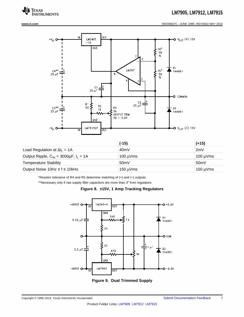
(-15) (+15)
Load Regulation at ΔIL = 1A 40mV 2mV
Output Ripple, CIN = 3000µF, IL = 1A 100 µVms 100 µVms
Temperature Stability 50mV 50mV
Output Noise 10Hz ≤ f ≤ 10kHz 150 µVms 150 µVms
*Resistor tolerance of R4 and R5 determine matching of (+) and (−) outputs.
**Necessary only if raw supply filter capacitors are more than 3″ from regulators.
Figure 8. ±15V, 1 Amp Tracking Regulators
Figure 9. Dual Trimmed Supply
Copyright © 1999–2013, Texas Instruments Incorporated Submit Documentation Feedback 7
Product Folder Links: LM7905 LM7912 LM7915

LM7905, LM7912, LM7915
SNOSBQ7C –JUNE 1999–REVISED MAY 2013 www.ti.com
Schematic Diagrams
Figure 10. −5V
Figure 11. −12V and −15V
8 Submit Documentation Feedback Copyright © 1999–2013, Texas Instruments Incorporated
Product Folder Links: LM7905 LM7912 LM7915

LM7905, LM7912, LM7915
www.ti.com SNOSBQ7C –JUNE 1999–REVISED MAY 2013
REVISION HISTORY
Changes from Revision B (May 2013) to Revision C Page
• Changed layout of National Data Sheet to TI format. ........................................................................................................... 8
Copyright © 1999–2013, Texas Instruments Incorporated Submit Documentation Feedback 9
Product Folder Links: LM7905 LM7912 LM7915

PACKAGE OPTION ADDENDUM
www.ti.com 30-Sep-2021
Addendum-Page 1
PACKAGING INFORMATION
Orderable Device Status(1)
Package Type PackageDrawing
Pins PackageQty
Eco Plan(2)
Lead finish/Ball material
(6)
MSL Peak Temp(3)
Op Temp (°C) Device Marking(4/5)
Samples
LM7905CT NRND TO-220 NDE 3 45 Non-RoHS& Green
Call TI Level-1-NA-UNLIM 0 to 125 LM7905CT
LM7905CT/NOPB ACTIVE TO-220 NDE 3 45 RoHS & Green SN Level-1-NA-UNLIM 0 to 125 LM7905CT
LM7912CT NRND TO-220 NDE 3 45 Non-RoHS& Green
Call TI Level-1-NA-UNLIM 0 to 125 LM7912CT
LM7912CT/NOPB ACTIVE TO-220 NDE 3 45 RoHS & Green SN Level-1-NA-UNLIM 0 to 125 LM7912CT
LM7915CT NRND TO-220 NDE 3 45 Non-RoHS& Green
Call TI Level-1-NA-UNLIM 0 to 125 LM7915CT
LM7915CT/NOPB ACTIVE TO-220 NDE 3 45 RoHS & Green SN Level-1-NA-UNLIM 0 to 125 LM7915CT
(1) The marketing status values are defined as follows:ACTIVE: Product device recommended for new designs.LIFEBUY: TI has announced that the device will be discontinued, and a lifetime-buy period is in effect.NRND: Not recommended for new designs. Device is in production to support existing customers, but TI does not recommend using this part in a new design.PREVIEW: Device has been announced but is not in production. Samples may or may not be available.OBSOLETE: TI has discontinued the production of the device.
(2) RoHS: TI defines "RoHS" to mean semiconductor products that are compliant with the current EU RoHS requirements for all 10 RoHS substances, including the requirement that RoHS substancedo not exceed 0.1% by weight in homogeneous materials. Where designed to be soldered at high temperatures, "RoHS" products are suitable for use in specified lead-free processes. TI mayreference these types of products as "Pb-Free".RoHS Exempt: TI defines "RoHS Exempt" to mean products that contain lead but are compliant with EU RoHS pursuant to a specific EU RoHS exemption.Green: TI defines "Green" to mean the content of Chlorine (Cl) and Bromine (Br) based flame retardants meet JS709B low halogen requirements of <=1000ppm threshold. Antimony trioxide basedflame retardants must also meet the <=1000ppm threshold requirement.
(3) MSL, Peak Temp. - The Moisture Sensitivity Level rating according to the JEDEC industry standard classifications, and peak solder temperature.
(4) There may be additional marking, which relates to the logo, the lot trace code information, or the environmental category on the device.
(5) Multiple Device Markings will be inside parentheses. Only one Device Marking contained in parentheses and separated by a "~" will appear on a device. If a line is indented then it is a continuationof the previous line and the two combined represent the entire Device Marking for that device.

PACKAGE OPTION ADDENDUM
www.ti.com 30-Sep-2021
Addendum-Page 2
(6) Lead finish/Ball material - Orderable Devices may have multiple material finish options. Finish options are separated by a vertical ruled line. Lead finish/Ball material values may wrap to twolines if the finish value exceeds the maximum column width.
Important Information and Disclaimer:The information provided on this page represents TI's knowledge and belief as of the date that it is provided. TI bases its knowledge and belief on informationprovided by third parties, and makes no representation or warranty as to the accuracy of such information. Efforts are underway to better integrate information from third parties. TI has taken andcontinues to take reasonable steps to provide representative and accurate information but may not have conducted destructive testing or chemical analysis on incoming materials and chemicals.TI and TI suppliers consider certain information to be proprietary, and thus CAS numbers and other limited information may not be available for release.
In no event shall TI's liability arising out of such information exceed the total purchase price of the TI part(s) at issue in this document sold by TI to Customer on an annual basis.

TUBE
*All dimensions are nominal
Device Package Name Package Type Pins SPQ L (mm) W (mm) T (µm) B (mm)
LM7905CT NDE TO-220 3 45 502 33 6985 4.06
LM7905CT NDE TO-220 3 45 502 33 6985 4.06
LM7905CT/NOPB NDE TO-220 3 45 502 33 6985 4.06
LM7912CT NDE TO-220 3 45 502 33 6985 4.06
LM7912CT NDE TO-220 3 45 502 33 6985 4.06
LM7912CT/NOPB NDE TO-220 3 45 502 33 6985 4.06
LM7915CT NDE TO-220 3 45 502 33 6985 4.06
LM7915CT NDE TO-220 3 45 502 33 6985 4.06
LM7915CT/NOPB NDE TO-220 3 45 502 33 6985 4.06
PACKAGE MATERIALS INFORMATION
www.ti.com 5-Jan-2022
Pack Materials-Page 1

MECHANICAL DATA
NDE0003B
www.ti.com

IMPORTANT NOTICE AND DISCLAIMERTI PROVIDES TECHNICAL AND RELIABILITY DATA (INCLUDING DATA SHEETS), DESIGN RESOURCES (INCLUDING REFERENCE DESIGNS), APPLICATION OR OTHER DESIGN ADVICE, WEB TOOLS, SAFETY INFORMATION, AND OTHER RESOURCES “AS IS” AND WITH ALL FAULTS, AND DISCLAIMS ALL WARRANTIES, EXPRESS AND IMPLIED, INCLUDING WITHOUT LIMITATION ANY IMPLIED WARRANTIES OF MERCHANTABILITY, FITNESS FOR A PARTICULAR PURPOSE OR NON-INFRINGEMENT OF THIRD PARTY INTELLECTUAL PROPERTY RIGHTS.These resources are intended for skilled developers designing with TI products. You are solely responsible for (1) selecting the appropriate TI products for your application, (2) designing, validating and testing your application, and (3) ensuring your application meets applicable standards, and any other safety, security, regulatory or other requirements.These resources are subject to change without notice. TI grants you permission to use these resources only for development of an application that uses the TI products described in the resource. Other reproduction and display of these resources is prohibited. No license is granted to any other TI intellectual property right or to any third party intellectual property right. TI disclaims responsibility for, and you will fully indemnify TI and its representatives against, any claims, damages, costs, losses, and liabilities arising out of your use of these resources.TI’s products are provided subject to TI’s Terms of Sale or other applicable terms available either on ti.com or provided in conjunction with such TI products. TI’s provision of these resources does not expand or otherwise alter TI’s applicable warranties or warranty disclaimers for TI products.TI objects to and rejects any additional or different terms you may have proposed. IMPORTANT NOTICE
Mailing Address: Texas Instruments, Post Office Box 655303, Dallas, Texas 75265Copyright © 2022, Texas Instruments Incorporated