… absorption properties of semiconducting nanostructures with different shapes hilal cansizoglu ,*...
TRANSCRIPT

158
FULL
PAPER
www.MaterialsViews.comwww.advopticalmat.de
Optical Absorption Properties of Semiconducting Nanostructures with Different Shapes
Hilal Cansizoglu ,* Mehmet F. Cansizoglu , Miria Finckenor , and Tansel Karabacak
In this study, a detailed experimental and theoretical investigation of optical absorption properties of indium sulfi de (In 2 S 3 ) nanostructure arrays in differ-ent shapes are presented. Zigzags, springs, screws, tilted rods, and vertical rods of In 2 S 3 are grown using a glancing angle deposition (GLAD) technique. Nanostructured coatings are of similar material volume and porosity, yet with different shapes. Total optical refl ection, transmission, and absorption profi les of In 2 S 3 nanostructures are obtained by UV-vis-NIR spectroscopy using an integrating sphere. Measurements reveal that optical absorption of semiconducting nanostructures can strongly depend on their shapes. Under normal incidence of light, 3D geometries such as springs, screws, and verti-cal rods can provide enhanced absorption compared to zigzags, and tilted rods. Results of fi nite difference time domain (FDTD) simulations predict that spring, screw, and tapered-rod shapes can introduce a uniform distribution of diffracted light intensity and stronger absorption within the nanostruc-tured layer, indicating an enhanced diffuse light scattering and light trapping. Zigzags and tilted rods show a relatively weaker absorption, similar to the experimental results. Experimental and simulation results are also compared to the predictions of effective medium theory. Current effective medium ap-proximations are not suffi cient to explain the high optical absorption of the nanostructures.
1 . Introduction
Over the past decades, utilization of nanostructured semicon-ductors in photovoltaics (PV) and photonics has mainly aimed to overcome problems associated with high fabrication costs, insuffi cient light absorption, and low conversion effi ciencies in conventional bulk and thin fi lm materials. [ 1,2 ] For instance, ZnO nanostructures as anti-refl ection layers, [ 3 ] anode TiO 2 nanostructures in dye-sensitized solar cells, [ 4 ] buffer layer of CdS nanowires in CdTe solar cells, [ 5 ] coaxial silicon nanowires for power sources in nanoelectronics, [ 6 ] In 2 S 3 nanoparticle photodetectors [ 7 ] are a few of the prominent examples of using
© 2013 WILEY-VCH Verlag GmbH & Co. KGaA, Weinheiwileyonlinelibrary.com
H. Cansizoglu, Dr. M. F. Cansizoglu, Dr. T. KarabacakDepartment of Applied Science University of Arkansas at Little Rock Little Rock , Arkansas , 72204 , USA E-mail: [email protected] M. Finckenor NASA Marshall Space Flight Center Alabama , 35812 , USA
DOI: 10.1002/adom.201200018
semiconductor nanostructures in phot-onics and photovoltaics due to their supe-rior optical and electrical properties. One of the most important characteristics of nanostructures for such applications is the optical absorption, which fundamen-tally depends on electronic band gap of the semiconductor material. However, in contrast to their thin fi lm counterparts, nanostructures can have different optical absorption spectra depending on their size, shape, and density. This has attracted the interest of researchers in recent years. These studies mainly focused on nanowire arrays of different diameter, length, and porosity. [ 8–13 ] Such physical parameters are of great importance due to their infl u-ence on light trapping and absorption. [ 8–13 ] In order to develop an effi cient light trap-ping, and therefore enhanced optical absorption, morphology and density of nanostructures need to be designed to provide low refl ection [ 14 ] and suffi cient dif-fuse light scattering. [ 9 ] In addition to diam-eter, [ 11,12 ] length, [ 8,12 ] and layer porosity, [ 13 ] which are known to affect surface refl ec-tion and light scattering properties, shape
of semiconducting nanostructures can also be of great impor-tance for enhanced light trapping and optical absorption. [ 15 ] However, to the best of our knowledge, effect of nanostructure shape on optical absorption has not been investigated in the literature extensively, which will be the focus of this work pre-sented here.
In this study, indium sulfi de (In 2 S 3 ) is chosen as the material of choice due to its advantageous properties in PV solar cell and photonic applications. In 2 S 3 is an n-type semiconducting mate-rial [ 16,17 ] with a relatively wide bandgap energy ranging between 1.9 eV and 3.3 eV depending on the details of fabrication method used [ 18–20 ] ∼ 2.0 eV being the most commonly reported band gap value for stoichiometric In 2 S 3 . Indium sulfi de thin fi lms are used as an environmental friendly alternative buffer layer to CdS in CuInSe 2 (CIS) and Cu(In,Ga)Se 2 (CIGS) solar cells, which avoids the need for heavily toxic Cd. [ 21 ] Besides its use in photovoltaics, In 2 S 3 is also a promising material in photo-detection applications. [ 7,22 ]
Arrays of In 2 S 3 nanostructures of this work were grown by glancing angle deposition (GLAD, also named oblique angle deposition) method. [ 22–25 ] GLAD offers the unique capability of controlling nanostructure shape through a physical self-assembly growth process. Nanostructured arrays in shapes
m Adv. Optical Mater. 2013, 1, 158–166

FULL P
APER
FULL P
APER
FULL P
APER
www.MaterialsViews.comwww.advopticalmat.de
Figure 1. (a) Glancing angle deposition (GLAD) method. Formation of tilted (b) and vertical (c) arrays of nanorods during GLAD are illustrated .
such as zigzags, springs, screws, vertical and tilted rods [ 26 ] can be easily produced by GLAD. [ 27 ] Another advantage of this growth method is to form well-aligned and well-separated nanostructures of a wide range of materials on almost any type of substrate.
GLAD is a physical vapor deposition method that utilizes a substrate modulator with axial tilt and radial rotation features. As illustrated in Figure 1 (a), axial rotation allows the ability to tilt the substrate with respect to the source-axis providing an obliquely incident fl ux of atoms on the substrate; while radial rotation determines the azimuthal direction at which atoms will approach on the substrate surface. GLAD uses high tilt (deposition) angles typically above 70°. At initial stages of the growth, there is random nucleation of islands. However, due to the oblique angle of the incident fl ux, islands of higher height shadow the neighboring surface locations and other smaller islands. Growth of shadowed regions becomes hindered, while on the other hand, islands of higher height grow faster. This so-called ‘shadowing effect’ introduces a physical self-assembly mechanism that leads to the growth of isolated nanostructure arrays.
For example, in the case of a stationary tilted substrate, nanostructures grow towards the incident fl ux resulting in arrays of tilted nanorods (Figure 1 (b)). When the substrate is radially rotated with 180° steps, fl ux successively coming from right and left sides of the substrate lead to the formation of zigzag shapes. If a continuous slow radial rotation is introduced, then nanostructures try to grow in a tilted way but at the same time follow the azimuthal change in the fl ux direction, which
© 2013 WILEY-VCH Verlag GAdv. Optical Mater. 2013, 1, 158–166
produces nanosprings or nanoscrews for slow and relatively faster rotation speeds, respectively. However, when the rotation speed exceeds a critical limit, which depends on the material and deposition rate, nanostructures cannot grow in sideways, resulting in the formation of vertical nanorods (Figure 1 (c)).
Previous studies on the optical properties of GLAD nanos-tructures focused mainly on the anti-refl ection properties [ 14,28 ] and optical transmission [ 29,30 ] characteristics of non-semicon-ducting materials. Recent work on GLAD semiconductor mate-rials [ 22,31–33 ] did not report on the optical absorption properties of nanostructures in different shapes.
Therefore, there has been a need for an in-depth investiga-tion of the effect of nanostructure shape on the optical absorp-tion of semiconducting materials. For this purpose, we present a detailed experimental and theoretical investigation of optical absorption properties of GLAD indium sulfi de (In 2 S 3 ) nanos-tructure arrays. Total optical refl ection and transmission pro-fi les were measured to extract and compare optical absorption of In 2 S 3 nanostructures of different shapes. Theoretical calcula-tions included numerical solutions of Maxwell’s equations and were performed with a commercial simulation tool (Lumerical Solutions) that uses a fi nite difference time domain (FDTD) approach. FDTD method has been proven to be an effi cient way of analyzing interaction of light with thin fi lm and nanos-tructured materials used in photovoltaics and photonics appli-cations. [ 34–37 ] In addition, we compare our experimental and numerical results to the predictions of effective medium theory, which has been another widely used theoretical method of mod-eling optical properties of porous or composite materials. [ 38,39 ]
159wileyonlinelibrary.commbH & Co. KGaA, Weinheim

160
FULL
PAPER
FULL
PAPER
FULL
PAPER
www.MaterialsViews.comwww.advopticalmat.de
Figure 2. Cross-sectional SEM images of GLAD indium sulfi de (In 2 S 3 ) (a) vertical nanorods, (b) nanoscrews, (c) nanosprings, (d) nanozigzags, and (e) tilted nanorods are illustrated .
2 . Results and Discussion
2.1 . Morphological Characterization
As-deposited thin fi lm and GLAD nano-structures of indium sulfi de were found to be stoichiometric In 2 S 3 , yet with an amorphous structure. [ 22 ] Independent of their shapes, the porosity of GLAD In 2 S 3 nanostructured layers (i.e. portion of gaps among nanostruc-tures wrt nominal thickness volume) was similar and estimated to be about 30% from the analysis of SEM images with a commer-cial computer software package (SPIP). This calculated porosity is in good agreement with our previous results. [ 22 ]
Figure 2 shows scanning electron micro-scopy (SEM) images of GLAD In 2 S 3 nanos-
tructure arrays of different shapes. Some of the SEM images look blurry due to sample charging, which arises from the relatively low electrical conductivity of nanostructured indium sulfi de, where isolated geometry further hinders the fl ow of charge.As can be seen in Figure 2 , morphology of nanostructure arrays is apparently different from each other. Nanorods, nanoscrews and nanosprings are vertically aligned due to continuous radial rotation. The fi ne structures of nanoscrews at the side walls and helical structure of nanosprings are formed as a result of relatively slow substrate rotation during deposition, as described before. On the other hand, nanozig-zags and tilted nanorods followed the fl ux direction leading to a ∼ 32° inclination angle (the angle between the tilted rod/zigzag arm and the surface). Height of the rods, springs, and screws is measured to be 250 nm, 240 nm, and 315 nm, respectively. The diameters vary between 70–90 nm for these three morphologies. Tilted rods and zigzags are about 250 nm thick, and have diameters of around 30 nm. All these nanos-tructure coatings have similar porosity and amount of mate-rial, except nanoscrew sample was slightly thicker than the others.
2.2 . Optical Characterization
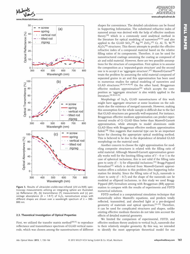
Figure 3 (a), (b) and (c) show wavelength dependent refl ect-ance (R), transmittance (T), and absorptance (A) spectra, respectively. A is calculated with the help of refl ectance and transmittance data through the relation A = 1-T-R. If the refl ection profi le of In 2 S 3 nanostructures of different shapes in Figure 3(a) is compared, one can see that they all show sim-ilar low refl ectance values over the entire spectrum. Especially at wavelengths shorter than 500 nm, the refl ectance is about 5%, which is signifi cantly lower compared to the 20–30% value of conventional smooth In 2 S 3 thin fi lms. [ 22 ] Suppression of refl ection gives GLAD nanostructures capability of acting as an antirefl ection layer. At shorter wavelengths, refl ectance is further reduced down to as low as 3%, which makes the absorptance values approaching about 97%. This is signifi -cantly higher than the optical absorption of much thicker and
wileyonlinelibrary.com © 2013 WILEY-VCH Verlag
denser fl at In 2 S 3 thin fi lms (e.g. maximum absorptance being ∼ 70% for a dense 730 nm thick In 2 S 3 fi lm grown at similar deposition conditions. [ 22 ] While refl ectivity does not seem to signifi cantly depend on nanostructure shape, transmission and absorption spectra may differ among nanostructure of different shapes considerably (Figure 3 (b),(c)). For example, zigzags, tilted rods, vertical rods, springs, and screws reach 50% absorption at wavelengths of 456, 472, 498, 502, and 516 nm, respectively. When we compare their average response over the entire spectrum, nanoscrews, nanorods, and nano-springs transmit less, and thus absorb more of the incident light compared to nanozigzags and tilted nanorods. Interest-ingly, nanoscrews had a similar absorption profi le to those of nanorods and nanosprings, although screws were about 30% longer than the later ones. This suggests that screws would show lower absorption if they had similar lengths with other samples.
Different profi les of optical absorption spectrum among nanostructures could be argued to be a result of change in their band gap values, since indium sulfi de’s band gap might vary depending on the deposition method. [ 18–20 ] However, we used identical deposition conditions to fabricate all of the In 2 S 3 sam-ples, and therefore we expect them to have similar band gap values. In addition, feature sizes of In 2 S 3 nanorods, nanoscrews and nanosprings that vary in the range of 70–90 nm (diameter) are not small enough to introduce any possible quantum-size effects, which typically occur at dimensions lower than Bohr exciton radius (33.8 nm for In 2 S 3 ). [ 40 ] Quantum-size effects might be considered for nanozigzags and tilted nanorods, which have diameters of approximately 30 nm, which is slightly lower than indium sulfi de’s Bohr exciton radius. However, nei-ther nanozigzags nor tilted nanorods show higher absorption at smaller wavelengths (which is a result of widening of band gap due to size effects); hence, this indicates that no measur-able quantum-size effect exists. Thus, shape of nanostructures is believed to be the main reason that leads to difference in optical absorption properties. In order to investigate the pos-sible effects of nanostructure shape on the optical absorption of semiconducting materials, below we will present the results from our theoretical studies that include numerical and analyt-ical modeling methods.
GmbH & Co. KGaA, Weinheim Adv. Optical Mater. 2013, 1, 158–166
FULL P
APER
FULL P
APER
FULL P
APER
www.MaterialsViews.comwww.advopticalmat.de
Figure 3. Results of ultraviolet–visible-near-infrared (UV-vis-NIR) spec-troscopy measurements utilizing an integrating sphere are illustrated. (a) Refl ectance (R), (b) transmittance (T) measurements and (c) per-centage absorptance (A = 1-R-T) of In 2 S 3 nanostructure arrays with different shapes are shown over a wavelength spectrum of λ = 300–800 nm .
300 400 500 600 700 8000
10
20
30
40
50O
ptic
al R
efle
ctan
ce (
%)
Wavelength (nm)
screw spring vertical rod tilted rod zigzag
(a)
300 400 500 600 700 800
0
20
40
60
80
100 (b)
Opt
ical
Tra
nsm
ittan
ce (
%)
Wavelength (nm)
screw spring vertical rod tilted rod zigzag
300 400 500 600 700 800
0
20
40
60
80
100 (c)
Opt
ical
Abs
orpt
ance
(%
)
Wavelength (nm)
screw spring vertical rod tilted rod zigzag
2.3 . Theoretical Investigation of Optical Properties
First, we utilized the transfer matrix method [ 38,41 ] to reproduce refl ectance and transmittance spectrum of GLAD vertical nano-rods, which was chosen among the nanostructures of different
© 2013 WILEY-VCH Verlag GmAdv. Optical Mater. 2013, 1, 158–166
shapes for convenience. The detailed calculations can be found in Supporting Information. The substituted refractive index of nanorod arrays was derived with the help of effective medium theory, [ 39 ] which is a commonly used analytical method in the literature for optical modeling of nanowires [ 42,43 ] and also applied to the GLAD SiO 2 , [ 28 ] Ag, [ 44 ] ZrO 2 , [ 45 ] Cr, Al, Ti, W, [ 38 ] Al 2 O 3 [ 46 ] structures. This theory attempts to predict the effective refractive index of a compound material based on the relative fi lling ratios of its components. Therefore, it can be used for nanostructured coatings assuming the coating as composed of air and solid material. However, there are two possible assump-tions for the structure of composition. First option is to assume the composition as a ‘separated-grain structure’ and the second one is to accept it as ‘aggregate structure’. [ 47 ] Maxwell-Garnet [ 48 ] treats the problem by assuming the solid material composed of separated grains in air and this approximation has been used in numerous studies for optical modeling of nanowires and GLAD structures. [ 28,43,44,46,49 ] On the other hand, Bruggeman effective medium approximation [ 50 ] which accepts the com-position as ‘aggregate structure’ is also widely applied in the literature. [ 30,38,42,45 ]
Morphology of In 2 S 3 GLAD nanostructures of this work might have aggregate structure at some locations on the sub-strate due the existence of merged nanorods. However, making this assumption for the whole sample is diffi cult due to the fact that GLAD structures are generally well-separated. For instance, Bruggeman effective medium approximation can predict exper-imental results of Cr GLAD fi lms better than Maxwell-Garnett approximation, while attempts to model aluminum oxide GLAD fi lms with Bruggeman effective medium approximation failed. [ 38 ] This suggests that material type can be an important factor for choosing the appropriate optical modeling method. This is believed to be due to the dependence of detailed GLAD morphology on the material used.
Another concern to choose the right approximation for mod-eling composite structures is related with the fi lling ratio of solid material. Although Maxwell-Garnett approximation gener-ally works well for the limiting fi lling ratios of f ∼ 0 or 1 in the case of spherical inclusions, this is not valid if the fi lling ratio goes to unity (f ∼ 1) for ellipsoidal inclusions. [ 51 ] Bragg-Pippard formalism [ 52 ] which is derived from Maxwell-Garnett approxi-mation offers a solution to this problem (See Supporting Infor-mation for details). Since the fi lling ratio of In 2 S 3 nanorods is closer to unity (f ∼ 0.7) and the shape of the nanorods can be modeled as ellipsoid inclusions, in this study we used Bragg-Pippard (BP) formalism among with Bruggeman (BR) approxi-mation to compare with the results of experiments and FDTD numerical solutions.
FDTD method is a computational simulation technique that numerically solves Maxwell’s equations, and predicts totally refl ected, transmitted, and absorbed light at a pre-designed geometry of materials and optical spectrum. [ 53–55 ] Therefore, it can be used for complicated structures and shapes, unlike existing effective medium theories do not take into account the effects of detailed material geometry.
We limited the comparison of experimental, FDTD, and effective medium theory analysis to vertical In 2 S 3 nanorods due to their relatively simpler geometry. By this way, we intended to identify the most appropriate theoretical model for our
161wileyonlinelibrary.combH & Co. KGaA, Weinheim
162
FULL
PAPER
FULL
PAPER
FULL
PAPER
www.MaterialsViews.comwww.advopticalmat.de
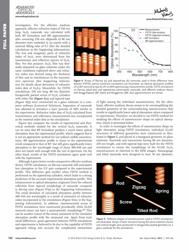
Figure 4. Arrays of fl at-top (a) and tapered-top (b) nanorods used in fi nite difference time domain (FDTD) optical numerical simulations are illustrated. (c) Optical absorption profi les of GLAD nanorod arrays by UV-vis-NIR spectroscopy measurements (solid), FDTD simulations on fl at-top (dash-dot) and tapered-top (short-dash) nanorods, and effective medium theory with Bragg-Pippard (BP, dash) and Bruggeman (BR, dot) approximations are shown.
300 400 500 600 700 800
0
20
40
60
80
100
Opt
ical
Abs
orpt
ance
(%
)
Wavelength (nm)
Measurement FDTD (flat surface) FDTD (tapered surface) BP formalism BR approximation
(c)
investigation. For the effective medium approach, effective refractive index of 250 nm long In 2 S 3 nanorods was calculated with both BP formalism and BR approximation after assuming 250 nm ellipsoids of 80 nm diameter were embeded in air matrix with a material fi lling ratio of 0.7 (See the detailed calculations in the Supporting Information). The real and imaginary parts of refractive index of In 2 S 3 were determined from the transmission and refl ection spectra of In 2 S 3 fi lm. For this purpose, In 2 S 3 fi lm was ther-mally deposited on glass substrate under the same conditions explained above and refrac-tive index was derived using the thickness of fi lm and its interferences in the transmis-sion spectrum (See Supporting Informa-tion for details about derivation of refractive index data of In 2 S 3 ). Meanwhile, for FDTD simulations, 250 nm long, 80 nm diameter hexagonally packed arrays of In 2 S 3 cylinders with either fl at ( Figure 4 (a)) and tapered topsFigure 5. Different shapes of nanostructures used in FDTD simulations are illustrated. Arrays of each structure having the same material volume and vertical length were positioned in hexagonally packed geometry on a glass substrate for the simulations.
(Figure 4(b)) were constructed on a glass substrate in a com-puter software (Lumerical Solutions). Separation of nanorods was adjusted to introduce a layer porosity of 30% similar to the experiments. Refractive index data of In 2 S 3 -calculated from transmittance and refl ectance measurements-was incorporated as the material index data in the simulations.
Figure 4 (c) compares the results of experimental and theo-retical methods studied for the vertical In 2 S 3 nanorods. It can be seen that BP formalism predicts a much lower optical absorption than the experimental profi le, which suggests that it is not an appropriate method for our indium sulfi de nanostruc-tures. BR approximation profi le is closer to the experimental result compared to that of BP, but still gives signifi cantly lower absorption in the wavelength range of about 300–450 nm and does not match well enough with the rest of spectrum. On the other hand, results of the FDTD simulations agree quite well with the experiments.
Although it gives better results compared to effective medium theory, FDTD calculations on fl at-top nanorods still anticipates less absorption in the UV part compared to the experimental profi le. This difference gets smaller when FDTD method is performed on the tapered-top cylinders, which leads to a strong prediction of the accurate experimental absorption profi le. This enhancement in optical absorption originates from the reduced refl ection from tapered morphology of nanorods compared to fl at-top ones (Figure S7(a) in the Supporting Information). The small deviation of calculated absorption profi le between 400–450 nm wavelengths is a result of mismatch of refractive index incorporated in the simulations (Figure S4(c) in the Sup-porting Information). In addition, nanostructured arrays of FDTD simulations were constructed periodically, while GLAD nanorod arrays can have a quasi-periodic morphology. [ 56 ] This can be another reason of the minor mismatch of the simulated absorption profi le with the measured one. Apart from such small differences, good agreement between FDTD simulations and experiments is believed to be due to the capability of FDTD approach taking into account the complicated interactions
wileyonlinelibrary.com © 2013 WILEY-VCH Verlag G
of light among the individual nanostructures. On the other hand, effective medium theory seems to be oversimplifying the detailed geometry of the semiconducting nanostructures that results in signifi cantly lower optical absorption values compared to experiments. Therefore, we decided to use FDTD method for studying the effects of nanostructure shape on optical absorp-tion, which is presented below.
In order to investigate the effects of nanostructure shape on light absorption using FDTD simulations, individual GLAD structures of different geometries were constructed as illus-trated in Figure 5 , and placed in a hexagonal geometry on glass substrate. Nanorods and nanoscrews having 80 nm diameter, 250 nm length, and with tapered tops were built for the FDTD simulations to mimic the morphology of the GLAD In 2 S 3 nanostructures as observed in the SEM images. Nanozigzags and tilted nanorods were designed to have 30 nm diameter,
mbH & Co. KGaA, Weinheim Adv. Optical Mater. 2013, 1, 158–166

FULL P
APER
FULL P
APER
FULL P
APER
www.MaterialsViews.comwww.advopticalmat.de
Figure 6. Results of FDTD simulations are illustrated. (a) Refl ectance (R), (b) transmittance (T), and (c) percentage absorptance (A = 1-R-T) of In 2 S 3 nanostructure arrays in different shapes are shown over a wavelength spectrum of λ = 300–800 nm . .
300 400 500 600 700 8000
5
10
15
20
25
30
35
40
45
50
)
%( ecnatc elfeR lac itp
O
Wavelength (nm)
screw spring vertical rod tilted rod zigzag
(a)
300 400 500 600 700 800
0
20
40
60
80
100
)%( ecnatti
msnarT lacitp
O
Wavelength (nm)
screw spring vertical rod tilted rod zigzag
(b)
300 400 500 600 700 800
0
20
40
60
80
100
Opt
ical
Abs
orpt
ance
(%
)
Wavelength (nm)
screw spring vertical rod tilted rod zigzag
(c)
250 nm vertical length, and were positioned at a 32° inclination angle.
To eliminate the effects of material volume (i.e. weight loading) and length on optical absorption, arrays of nanostruc-tures were designed to have the same porosity value of 30% and same length of 250 nm. Numerical calculations were per-formed using p-polarized and s-polarized plane-wave sources, followed by taking the average of their optical power refl ectance, transmittance, and absorptance values in order to simulate the unpolarized light in experiments. Simulations were held under normal incidence light.
Figure 6 summarizes the results of FDTD calculations for nanostructure arrays in different shapes. As shown in Figure 6 (a), all of the structures refl ect around 5–10% of inci-dent light in UV part of the spectrum, which agrees well with the experimental profi les shown in Figure 3 (a). However, at longer wavelengths, interference peaks of FDTD profi les in Figure 6 (a) fl uctuate around 5–35%, while experimental pro-fi les showed a weaker interference pattern at similar wave-lengths and refl ectance peaks were within ∼ 5–15%. Reduced refl ection fl uctuations appeared in the experimental spectrum (Figure 3 (a)) is believed to be due to quasi-periodic structure of GLAD arrays, which disrupts the constructive/destructive inter-ference patterns. [ 13,56,57 ] However, spectrum-average refl ect-ance values of nanostructures of different shapes are all within 10–15%, which are quite close to the measured ones that range between 5–10%.
Although average refl ectance does not seem to have a strong dependence on the detailed geometry of nanostructures, trans-mittance and optical absorptance show a different trend as can be seen in Figure 6 (b) and (c). Nanorods, nanoscrews, and nanosprings transmit less and thus absorb more light compared to nanozigzags and tilted nanorods similar to the experimental results (Figure 3 (b) and (c)). When compared in more detail, FDTD simulations predict that nanostructures of different shapes will have optical absorption in the order: ver-tical-rods > screws > springs > zigzags > tilted-rods. In experi-mental results, nanoscrews had an absorption profi le slightly higher than that of vertical nanorods, while on the other hand, opposite was observed in simulation results. Higher absorption of screws in experiments is believed to be due to their slightly longer height.
Since the material loading, vertical length, and therefore layer porosity of the nanostructures were kept constant during simulations, the difference in their absorption spectrum is believed to be arisen from the shape effect. Refl ectance is expected to be more dependent on the top morphology of the layer where light primarily interacts. However, once light pen-etrates into the coating, detailed 3D geometry of the nanostruc-tures can strongly affect the interference, diffuse scattering, transmittance, and therefore light trapping of the layer. [ 13,15 ] For example, nanoscrews in FDTD simulations show a relatively higher refl ectance compared to other shapes (Figure 3 (a)), yet it shows the lowest transmittance among all (Figure 3 (b)) leading to a high optical absorption. In other words, our theoretical cal-culations suggest that high refl ectance from a nanostructured fi lm does not necessary mean that optical absorption will be low. One should consider the detailed geometry of nanostruc-tures and perform optical absorption calculations through total
© 2013 WILEY-VCH Verlag GAdv. Optical Mater. 2013, 1, 158–166
refl ectance and transmittance measurements ( e.g. using an integrating sphere as in our experiments), which will take into account both specular and diffuse refl ected/transmitted light. We note that these results and observations are believed to be valid for other semiconducting and light absorbing materials in general; however, might not apply to high refl ective and trans-parent coatings.
163wileyonlinelibrary.commbH & Co. KGaA, Weinheim

164
FULL
PAPER
FULL
PAPER
FULL
PAPER
www.MaterialsViews.comwww.advopticalmat.de
Figure 7. Cross sectional optical power intensity and absorption-per-unit-volume profi les of GLAD nanostructures of different shapes were calculated by FDTD simulations for wavelengths λ = 300, 400, 500 nm .
In order to obtain a more detailed understanding of interac-tion of light with the nanostructured material, we calculated the distribution of optical power intensity and absorption-per-unit-volume within the 3D geometry of the nanostructured layer of different shapes using FDTD simulations. Results are presented in Figure 7 . Power intensity can be helpful to better under-stand where light is mainly confi ned, while absorption-per-unit-volume is an indication of local optical absorption at a given sec-tion of the material. Therefore, these plots can provide detailed information on the light trapping and absorption behavior of a nanostructured coating. FDTD calculations shown in Figure 7 were performed for three different wavelengths of 300, 400, 500 nm. Figure 7 also lists the total absorptance percentages at given wavelengths for each different nanostructure shape.
Figure 7 shows that distribution of power intensity and absorption profi les within the nanostructured layer strongly depends on the nanostructure geometry. Overall, zigzag and
wileyonlinelibrary.com © 2013 WILEY-VCH Verlag
tilted nanostructures absorb more towards at their top surface, and therefore behave more like a fi lm. On the other hand, ver-tical rods, screws, and springs “guide” light deeper into the coating and results in enhanced absorption at the sidewalls and the interior of the nanostructures. Especially at longer wave-lengths such as λ = 500 nm in Figure 7 , this difference is more visible. Regular interference patterns of high/low intensity and absorption are apparent in zigzag and tilted geometries. How-ever, it is disrupted for the others, more notably in springs and screws, and also in vertical rods to some extent. This can be due to more complicated 3D geometry of shapes such as springs, screws, and rods (tapered), which can break down the interfer-ence patterns and leads to a more uniform distribution of light in the layer. In other words, this indicates an enhanced diffuse light scattering behavior of springs, screws, and tapered rods.
Results in Figure 7 also suggest that depending on the wave-length of interest and nanostructure geometry, a proper coating
GmbH & Co. KGaA, Weinheim Adv. Optical Mater. 2013, 1, 158–166

FULL P
APER
FULL P
APER
FULL P
APER
www.MaterialsViews.comwww.advopticalmat.de
thickness can be designed. For example, at shorter wavelengths such as λ = 300 nm, indium sulfi de nanostructures absorb most of the light at the upper ∼ 100 nm region, so nanostructures longer than this value might not be needed. However, when a more uniform distribution of light intensity and absorption in the coating is desired, as in the case of radial p–n junction nanostructured solar cells, shapes of springs, screws, and ver-tical tapered-rods would be a better choice even at short wave-lengths. If total absorption is more of a concern, vertical tapered-rods would be preferable. Briefl y, introducing 3D geometries can signifi cantly enhance the light trapping and optical absorp-tion properties of semiconducting nanostructures.
3 . Conclusion
In conclusion, we showed through our experimental and theoretical studies that optical absorption of semiconducting nanostructured materials can strongly depend on the detailed nanostructure shape. 3D geometries such as nanosprings, nanoscrews, and tapered vertical nanorods can provide an enhanced light trapping and absorption property compared to nanozigzags, and tilted nanorods under normal incidence of light. We also compared results of analytical calculations of effective medium theory with our experimental measurements and results of numerical calculations by FDTD simulations. Our detailed analysis shows that existing effective medium approxi-mations are not suffi cient enough to explain the higher optical absorption of nanostructures, especially at shorter wavelengths. On the other hand, FDTD simulations successfully predicted the experimental results. In addition, detailed calculations of FDTD simulations reveal that spring, screw, and tapered-rod shapes can introduce a uniform distribution of light intensity and absorption within the nanostructured layer, indicating the properties of enhanced diffuse light scattering and light trap-ping. On the other hand, zigzag and tilted structures absorb mainly at top portions of the coating, behaving more like a conventional thin fi lm. Optical absorption properties of these nanostructures under off-normal angle incidence of light are currently under investigation.
4 . Experimental Section Fabrication of Indium Sulfi de Nanostructures : In 2 S 3 nanostructures
in different shapes were deposited on glass substrates in a custom designed vacuum thermal evaporation GLAD system. 99.99% purity In 2 S 3 powder (from CERAC) was used as the evaporation source material. GLAD experiments were carried out at room temperature under 7.5 × 10 −6 torr base pressure with a deposition rate of 0.2 nm/s (i.e. nanostructure length/deposition time), which was measured by quartz crystal microbalance (QCM) and confi rmed by the analysis of cross-sectional scanning electron microscopy (SEM, JEOL 7000F) images. Samples were positioned at an 85 ° incidence angle measured between the incident fl ux and the substrate normal. In addition, a continuous rotation around the substrate normal axis was applied at a speed of 4, 1, and 0.2 rotation-per-minute (RPM) to form vertical nanorods, nanoscrews and nonosprings, respectively. For zig-zags, sample was rotated three times with steps of 180 ° at equal time intervals during the deposition, and no rotation was used for the growth of tilted nanorods.
© 2013 WILEY-VCH Verlag GAdv. Optical Mater. 2013, 1, 158–166
Morphological Characterization: Morphological characterization of In 2 S 3 nanostructures in different shapes were done by Scanning Electron Microscopy (SEM, JEOL 7000F).
Refl ection and Transmission Measurements: Total optical refl ection and transmission profi les of In 2 S 3 nanostructures were obtained by UV-vis-NIR spectroscopy measurements utilizing an integrating sphere (Shimadzu UV-3600). Light source was incident at a near-normal angle of 8° on the samples for refl ectance measurements.
Supporting Information Supporting Information is available from the Wiley Online Library or from the author.
Acknowledgements This work was supported by NASA under the grant number NNX09AW22A. The authors thank Dr.Yang Xu and UALR Center for Integrative Nanotechnology Sciences for helping with SEM and UV-vis-NIR spectroscopy measurements .
Received: October 21, 2012Revised: December 5, 2012
Published online: February 12, 2013
[1] H. Tsubomura , H. Kobayashi , Crit. Rev. Solid State 1993 , 18 , 261 . [2] G. Q. Zhang , S. Finefrock , D. X. Liang , G. G. Yadav , H. R. Yang ,
H. Y. Fang , Y. Wu , Nanoscale 2011 , 3 , 2430 . [3] Y. J. Lee , D. S. Ruby , D. W. Peters , B. B. McKenzie , J. W. P. Hsu ,
Nano Lett. 2008 , 8 , 1501 . [4] B. Oregan , M. Gratzel , Nature 1991 , 353 , 737 . [5] Z. Y. Fan , H. Razavi , J. W. Do , A. Moriwaki , O. Ergen , Y. L. Chueh ,
P. W. Leu , J. C. Ho , T. Takahashi , L. A. Reichertz , S. Neale , K. Yu , M. Wu , J. W. Ager , A. Javey , Nat. Mater. 2009 , 8 , 648 .
[6] B. Z. Tian , X. L. Zheng , T. J. Kempa , Y. Fang , N. F. Yu , G. H. Yu , J. L. Huang , C. M. Lieber , Nature 2007 , 449 , 885 .
[7] J. Tang , G. Konstantatos , S. Hinds , S. Myrskog , A. G. Pattantyus-Abraham , J. Clifford , E. H. Sargent , ACS Nano 2009 , 3 , 331 .
[8] L. Hu , G. Chen , Nano Lett. 2007 , 7 , 3249 . [9] E. Garnett , P. D. Yang , Nano Lett. 2010 , 10 , 1082 . [10] O. L. Muskens , J. G. Rivas , R. E. Algra , E. P. A. M. Bakkers ,
A. Lagendijk , Nano Lett. 2008 , 8 , 2638 . [11] Z. Y. Fan , R. Kapadia , P. W. Leu , X. B. Zhang , Y. L. Chueh , K. Takei ,
K. Yu , A. Jamshidi , A. A. Rathore , D. J. Ruebusch , M. Wu , A. Javey , Nano Lett. 2010 , 10 , 3823 .
[12] R. Tena-Zaera , J. Elias , C. Levy-Clement , Appl. Phys. Lett. 2008 , 93 , 233119.
[13] M. D. Kelzenberg , S. W. Boettcher , J. A. Petykiewicz , D. B. Turner-Evans , M. C. Putnam , E. L. Warren , J. M. Spurgeon , R. M. Briggs , N. S. Lewis , H. A. Atwater , Nat. Mater. 2010 , 9 , 368 .
[14] J. Q. Xi , M. F. Schubert , J. K. Kim , E. F. Schubert , M. F. Chen , S. Y. Lin , W. Liu , J. A. Smart , Nat. Photonics 2007 , 1 , 176 .
[15] S. L. Diedenhofen , O. T. A. Janssen , G. Grzela , E. P. A. M. Bakkers , J. G. Rivas , ACS Nano 2011 , 5 , 2316 .
[16] R. Yoosuf , M. K. Jayaraj , Sol. Energ. Mat. Sol. C 2005 , 89 , 85 . [17] H. M. Pathan , C. D. Lokhande , S. S. Kulkarni , D. P. Amalnerkar ,
T. Seth , S. H. Han , Mater. Res. Bull. 2005 , 40 , 1018 . [18] W. T. Kim , W. S. Lee , C. S. Chung , C. D. Kim , J. Appl. Phys. 1988 , 63 ,
5472 .
165wileyonlinelibrary.commbH & Co. KGaA, Weinheim

166
FULL
PAPER
FULL
PAPER
FULL
PAPER
www.MaterialsViews.comwww.advopticalmat.de
[19] P. M. R. Kumar , T. T. John , C. S. Kartha , K. P. Vijayakumar , T. Abe , Y. Kashiwaba , J. Mater. Sci. 2006 , 41 , 5519 .
[20] A. Timoumi , H. Bouzouita , R. Brini , M. Kanzari , B. Rezig , Appl. Surf. Sci. 2006 , 253 , 306 .
[21] N. Naghavi , D. Abou-Ras , N. Allsop , N. Barreau , S. Bucheler , A. Ennaoui , C. H. Fischer , C. Guillen , D. Hariskos , J. Herrero , R. Klenk , K. Kushiya , D. Lincot , R. Menner , T. Nakada , C. Platzer-Bjorkman , S. Spiering , A. N. Tiwari , T. Torndahl , Prog. Photovoltaics 2010 , 18 , 411 .
[22] M. F. Cansizoglu , R. Engelken , H. W. Seo , T. Karabacak , ACS Nano 2010 , 4 , 733 .
[23] N. O. Young , J. Kowal , Nature 1959 , 183 , 104 . [24] K. Robbie , M. J. Brett , A. Lakhtakia , Nature 1996 , 384 , 616 . [25] T. Karabacak , T. M. Lu, Handbook of Theoretical and Computational
Nanotechnology (Eds: M. Rieth , W. Schommers ), Scientifi c Pub-lishers , Stevenson Ranch, CA 2005 , p. 729 .
[26] C. Patzig , A. Miessler , T. Karabacak , B. Rauschenbach , Phys. Status Solidi B 2010 , 247 , 1310 .
[27] T. Karabacak , G. C. Wang , T. M. Lu , J. Vac. Sci. Technol. A 2004 , 22 , 1778 .
[28] S. R. Kennedy , M. J. Brett , Appl. Optics 2003 , 42 , 4573 . [29] A. C. van Popta , J. C. Sit , M. J. Brett , Appl. Optics 2004 , 43 ,
3632 . [30] G. W. Mbise , G. A. Niklasson , C. G. Granqvist , S. Palmer , J. Appl.
Phys. 1996 , 80 , 5361 . [31] K. Kaminska , T. Brown , G. Beydaghyan , K. Robbie , Appl. Optics 2003 ,
42 , 4212 . [32] F. C. Akkari , M. Kanzari , B. Rezig , Physica E 2008 , 40 , 2577 . [33] W. K. Choi , L. Li , H. G. Chew , F. Zheng , Nanotechnology 2007 , 18 ,
385302. [34] K. G. Ong , O. K. Varghese , G. K. Mor , K. Shankar , C. A. Grimes , Sol.
Energ. Mat. Sol. C 2007 , 91 , 250 .
wileyonlinelibrary.com © 2013 WILEY-VCH Verlag
[35] V. E. Ferry , A. Polman , H. A. Atwater , ACS Nano 2011 , 5 , 10055 . [36] J. Y. Tang , Z. Y. Huo , S. Brittman , H. W. Gao , P. D. Yang , Nat. Nano-
technol. 2011 , 6 , 568 . [37] J. K. Hyun , L. J. Lauhon , Nano Lett. 2011 , 11 , 2731 . [38] G. W. Mbise , D. LeBellac , G. A. Niklasson , C. G. Granqvist , J. Phys.
D Appl. Phys. 1997 , 30 , 2103 . [39] D. E. Aspnes , Thin Solid Films 1982 , 89 , 249 . [40] P. T. Zhao , T. Huang , K. X. Huang , J. Phys. Chem. C 2007 , 111 ,
12890 . [41] G. B. Smith , Appl. Optics 1990 , 29 , 3685 . [42] J. B. Baxter , C. A. Schmuttenmaer , J. Phys. Chem. B 2006 , 110 ,
25229 . [43] M. R. Black , Y. M. Lin , S. B. Cronin , O. Rabin , M. S. Dresselhaus ,
Phys. Rev. B 2002 , 65 , 195417. [44] Q. Zhou , Y. P. He , J. Abell , Z. J. Zhang , Y. P. Zhao , J. Phys. Chem. C
2011 , 115 , 14131 . [45] J. G. Wang , H. Shao , Z. X. Fan , Opt. Commun. 2005 , 247 , 107 . [46] D. Lebellac , G. A. Niklasson , C. G. Granqvist , J. Appl. Phys. 1995 , 78 ,
2894 . [47] G. A. Niklasson , C. G. Granqvist , O. Hunderi , Appl. Optics 1981 , 20 ,
26 . [48] J. C. Maxwell-Garnett , Philos. Trans. R. Soc. London A 1904 , 203 ,
385 . [49] M. Suzuki , Y. Taga , J. Appl. Phys. 1992 , 71 , 2848 . [50] D. A. G. Bruggeman , Ann. Phys. 1935 , 24 , 636 . [51] J. A. Sherwin , A. Lakhtakia , Microw. Opt. Techn. Lett. 2002 , 33 , 40 . [52] W. L. Bragg , A. B. Pippard , Acta Cryst. 1953 , 6 , 865 . [53] K. S. Yee , IEEE T. Antenn. Propag. 1966 , Ap14 , 302 . [54] A. Tafl ove , Wave Motion 1988 , 10 , 547 . [55] A. Tafl ove , IEEE T. Electromagn. C 1980 , 22 , 191 . [56] T. Karabacak , G. C. Wang , T. M. Lu , J. Appl. Phys. 2003 , 94 , 7723 . [57] H. Bao , X. L. Ruan , Opt Lett. 2010 , 35 , 3378 .
GmbH & Co. KGaA, Weinheim Adv. Optical Mater. 2013, 1, 158–166