zynq ultrascale+ rfsoc rf data converter v2.0 … · chapter 1 i p f a c t s the xilinx®...
TRANSCRIPT

Zynq UltraScale+ RFSoC RFData Converter 2.0
LogiCORE IP Product GuideVivado Design Suite
PG269 (v2.0) April 17, 2018

Table of ContentsChapter 1: IP Facts......................................................................................................... 4
Features........................................................................................................................................4IP Facts..........................................................................................................................................5
Chapter 2: Overview......................................................................................................6RF-ADC.......................................................................................................................................... 8RF-DAC........................................................................................................................................ 11Licensing and Ordering............................................................................................................ 13
Chapter 3: Product Specification......................................................................... 14Performance.............................................................................................................................. 16Resource Use............................................................................................................................. 16Port Descriptions.......................................................................................................................16Register Space........................................................................................................................... 21
Chapter 4: Designing with the Core................................................................... 32IP Core Configuration in Vivado Design Suite....................................................................... 32Software Driver..........................................................................................................................32RF-ADC........................................................................................................................................ 32RF-DAC........................................................................................................................................ 65Quadrature Modulator Correction .........................................................................................91Dynamic Update Events........................................................................................................... 94PLL...............................................................................................................................................95Interrupt Handling.................................................................................................................... 97Clocking.................................................................................................................................... 100Resets........................................................................................................................................105Power-up Sequence................................................................................................................ 106Interfacing to the AXI4-Stream Interface.............................................................................108Applications..............................................................................................................................109
Chapter 5: Design Flow Steps...............................................................................122Customizing and Generating the Core.................................................................................122
PG269 (v2.0) April 17, 2018 www.xilinx.com [placeholder text]Zynq UltraScale+ RFSoC RF Data Converter 2Send Feedback
Simulation................................................................................................................................ 134Synthesis and Implementation............................................................................................. 134
Chapter 6: Example Design................................................................................... 135RF-ADC Sink..............................................................................................................................136RF-DAC Source......................................................................................................................... 136Digital Data Format.................................................................................................................138
Chapter 7: Test Bench...............................................................................................139Analog Signaling..................................................................................................................... 140
Appendix A: Upgrading........................................................................................... 142Changes from V1.2 to V2.0..................................................................................................... 142Changes from V1.1 to V1.2..................................................................................................... 142
Appendix B: Debugging...........................................................................................144Finding Help on Xilinx.com.................................................................................................... 144Debug Tools............................................................................................................................. 145Hardware Debug..................................................................................................................... 146Interface Debug...................................................................................................................... 146
Appendix C: Zynq UltraScale+ RFSoC Data Converter Bare-metal/Linux Driver................................................................................................ 148Overview...................................................................................................................................148Data Structures........................................................................................................................149User API Functions.................................................................................................................. 163Interrupt Handling.................................................................................................................. 194In-line Functions......................................................................................................................199
Appendix D: Additional Resources and Legal Notices........................... 209Xilinx Resources.......................................................................................................................209Documentation Navigator and Design Hubs...................................................................... 209References................................................................................................................................210Training Resources..................................................................................................................210Revision History.......................................................................................................................210Please Read: Important Legal Notices................................................................................. 211
PG269 (v2.0) April 17, 2018 www.xilinx.com [placeholder text]Zynq UltraScale+ RFSoC RF Data Converter 3Send Feedback

Chapter 1
IP FactsThe Xilinx® LogiCORE™ IP Zynq® UltraScale+™ RFSoC RF Data Converter IP core provides aconfigurable wrapper to allow the RF-DAC and RF-ADC blocks to be used in IP integratordesigns.
Features• Up to 16 14-bit 6.5 GSPS RF-DACs
• Eight 12-bit 4 GSPS RF-ADCs, or 16 12-bit 2 GSPS RF-ADCs, depending on device
• Supports alignment between multiple converters
• Pre-programs RF-DAC and RF-ADC with key user-defined parameters
• Multiple AXI4-Stream data interfaces for RF-ADCs and RF-DACs
• Single AXI4-Lite configuration interface
• 1x (bypass), 2x, 4x, 8x interpolation
• 1x (bypass), 2x, 4x, 8x decimation
• Digital complex mixers
• Numerical Controlled Oscillator (NCO)
• Quadrature Modulation Correction (QMC)
In this guide reference is made to the 2 GSPS RF-ADC, the 4 GSPS RF-ADC, and the 6.5 G RF-DAC; for the actual sampling rate specifications, see the Zynq UltraScale+ RFSoC Data Sheet: DCand AC Switching Characteristics (DS926)
Chapter 1: IP Facts
PG269 (v2.0) April 17, 2018 www.xilinx.com [placeholder text]Zynq UltraScale+ RFSoC RF Data Converter 4Send Feedback

IP Facts
LogiCORE IP Facts TableCore Specifics
Supported Device Family1 Zynq® UltraScale+™ RFSoC
Supported User Interfaces AXI4-Stream, AXI4-Lite Control/Status
Resources Performance and Resource Use web page
Provided with Core
Design Files RTL
Example Design Verilog
Test Bench Verilog
Constraints File Xilinx Design Contstraints (XDC)
Simulation Model Verilog
Supported S/W Driver Standalone and Linux
Tested Design Flows2
Design Entry Vivado® IP Integrator
Simulation For supported simulators, see the Xilinx Design Tools:Release Notes Guide.
Synthesis Vivado Synthesis
Support
Provided by Xilinx at the Xilinx Support web page
Notes:
1. For a complete list of supported devices, see the Vivado® IP catalog.2. For the supported versions of the tools, see the Xilinx Design Tools: Release Notes Guide.
Chapter 1: IP Facts
PG269 (v2.0) April 17, 2018 www.xilinx.com [placeholder text]Zynq UltraScale+ RFSoC RF Data Converter 5
Send Feedback

Chapter 2
OverviewThe Xilinx® Zynq® UltraScale+™ RFSoC family integrates the key subsystems required toimplement a complete software-defined radio including direct RF sampling data converters,enabling CPRI and Gigabit Ethernet-to-RF on a single, highly programmable SoC.
Each RFSoC offers multiple RF-sampling analog-to-digital (RF-ADC) and RF-sampling digital-to-analog (RF-DAC) data converters. The data converters are high-precision, high-speed and power-efficient. Both are highly configurable and tightly integrated with the programmable logic (PL)resources of the Zynq UltraScale+ RFSoC.
The RF-ADC supports a sample rate of over 4 GSPS (see the Zynq UltraScale+ RFSoC Data Sheet:DC and AC Switching Characteristics (DS926) for the exact sample rate) and input signalfrequencies up to 4 GHz, with excellent noise spectral density. The RF-DAC generates outputcarrier frequencies up to 4 GHz while operating in the second Nyquist zone with excellent noisespectral density at a sample rate of over 6.5 GSPS (see the Zynq UltraScale+ RFSoC Data Sheet: DCand AC Switching Characteristics (DS926) for the exact sample rate). The RF data converters alsoinclude power efficient digital down converters (DDCs) and digital up converters (DUCs) thatinclude programmable interpolation and decimation rates, a numerically controlled oscillator(NCO), and a complex mixer. The DDCs and DUCs can also support dual-band operation. Thefollowing figure shows the block diagram of the Zynq® UltraScale+™ RFSoC RF Data Converter.
The RF-ADCs and RF-DACs are organized into tiles, each containing four RF-DACs or two orfour RF-ADCs. Multiple tiles are available in each Zynq® UltraScale+™ RFSoC (see the specificdevice data sheet for the number of tiles and converters per device). Each tile also includes ablock with a PLL and all the necessary clock handling logic and distribution routing for the analogand digital logic.
This guide describes the Zynq® UltraScale+™ RFSoC RF Data Converter IP core and softwaredrivers that are used to configure the data converters and instantiate them for use in a design. Inthis guide, reference is made to the 2 GSPS RF-ADC RF-ADC, the 4 GSPS RF-ADC, and the 6.5 GRF-DAC; for the actual sampling rate specifications see the Zynq UltraScale+ RFSoC Data Sheet:DC and AC Switching Characteristics (DS926)
For device specifications and additional information, see:
• Zynq UltraScale+ RFSoC Data Sheet: Overview (DS889)
• Zynq UltraScale+ RFSoC Data Sheet: DC and AC Switching Characteristics (DS926)
• Zynq UltraScale+ Device Technical Reference Manual (UG1085).
Chapter 2: Overview
PG269 (v2.0) April 17, 2018 www.xilinx.com [placeholder text]Zynq UltraScale+ RFSoC RF Data Converter 6Send Feedback

Figure 1: Zynq® UltraScale+™ RFSoC RF Data Converter IP Core in Zynq UltraScale+RFSoC
Zynq UltraScale+ RFSoC
Control and Configuration
Data Converter IP Core
Processing SystemQuad ARM Cortex-A53Dual ARM Cortex-R5
GTY SerialTransceivers
ProgrammableLogic
DUC
AXI4-Stream
DUC
AXI4-Stream
8 to 16 TX Channels
DDC
AXI4-Stream
DDC
AXI4-Stream8 to 16 RX Channels
AXI4-Lite
DAC
DAC
ADC
ADC
X19532-032718
Figure 2: Converter Tile Structure
DAC_X0Y0
Data Path 2 DAC2
Data Path 3 DAC3
Data Path 1 DAC1
Data Path 0 DAC0
IP StateMachine
s03_axis
s02_axis
s01_axis
s00_axis
6.5 GSPS RF-DAC Tile
ADC_X0Y1
Data Path 2 ADC2
Data Path 3 ADC3
Data Path 1 ADC1
Data Path 0 ADC0
m13_axis
m12_axis
m11_axis
m10_axis
2 GSPS RF-ADC Tile
ADC_X0Y0
Data Path 1(23)
ADC1(23)
Data Path 0(01)
ADC0(01)
m03_axis
m02_axis
m01_axis
m00_axis
4 GSPS RF-ADC Tile
IP StateMachine
IP StateMachine
X19519-032718
Chapter 2: Overview
PG269 (v2.0) April 17, 2018 www.xilinx.com [placeholder text]Zynq UltraScale+ RFSoC RF Data Converter 7Send Feedback
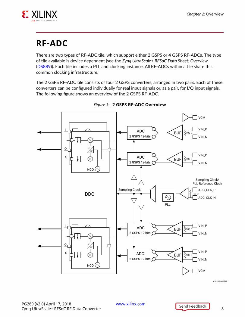
RF-ADCThere are two types of RF-ADC tile, which support either 2 GSPS or 4 GSPS RF-ADCs. The typeof tile available is device dependent (see the Zynq UltraScale+ RFSoC Data Sheet: Overview(DS889)). Each tile includes a PLL and clocking instance. All RF-ADCs within a tile share thiscommon clocking infrastructure.
The 2 GSPS RF-ADC tile consists of four 2 GSPS converters, arranged in two pairs. Each of theseconverters can be configured individually for real input signals or, as a pair, for I/Q input signals.The following figure shows an overview of the 2 GSPS RF-ADC.
Figure 3: 2 GSPS RF-ADC Overview
0°
90°
NCOQ
Q
I VIN_PADC2 GSPS 12-bits VIN_N
VIN_PADC2 GSPS 12-bits VIN_N
VCM
VIN_PADC2 GSPS 12-bits VIN_N
VIN_PADC2 GSPS 12-bits VIN_N
VCM
DDCADC_CLK_P
ADC_CLK_N
PLL
BUF 100 Ω
100 Ω BUF
100 Ω BUF
100 Ω BUF
Sampling Clock
NCO
0°
90°
NCOQ
Q
I
NCO
0°
90°
0°
90°
100 Ω
Sampling Clock/PLL Reference Clock
X18282-040518
Chapter 2: Overview
PG269 (v2.0) April 17, 2018 www.xilinx.com [placeholder text]Zynq UltraScale+ RFSoC RF Data Converter 8Send Feedback

The 4 GSPS RF-ADC tile consists of two 4 GSPS converters. These converters can be configuredindividually for real input signals or, as a pair, for I/Q input signals. The following figure shows anoverview of the 4 GSPS RF-ADC.
Figure 4: 4 GSPS RF-ADC Overview
RF ADC4GS/s 12-bits
RF ADC4GS/s 12-bits
Q
I
VIN_PADC4 GSPS 12-bits VIN_N
VCM
VIN_PADC4 GSPS 12-bits VIN_N
VCM
DDCADC_CLK_P
ADC_CLK_N
PLL
BUF 100 Ω
100 Ω BUF
Sampling Clock
0°
90°
NCO
Q
0°
90°
NCO
I
100 Ω
Sampling Clock/PLL Reference Clock
X18283-040518
RF-ADC Features• Tile configuration
Four RF-ADCs and one PLL per tile
12-bit RF-ADC resolution, with 16-bit digital signal processing datapath
Chapter 2: Overview
PG269 (v2.0) April 17, 2018 www.xilinx.com [placeholder text]Zynq UltraScale+ RFSoC RF Data Converter 9Send Feedback

Implemented as either four channels of 2 GSPS, or two channels of 4 GSPS (devicedependent; for the actual sampling rate specifications, see the Zynq UltraScale+ RFSoC DataSheet: DC and AC Switching Characteristics (DS926))
• Decimation filters
1x (bypass filter), 2x, 4x, 8x
80% of Nyquist bandwidth, 89 dB stop-band attenuation
• Digital Complex Mixers
Full complex mixers support real or I/Q inputs from the RF-ADC
48-bit Numeric Controlled Oscillator (NCO) per RF-ADC
Fixed Fs/4, Fs/2 low power frequency mixing mode, where Fs is the sample frequency
I/Q and real input signals supported
• Single/multi-band flexibility
2x bands per 2 GSPS RF-ADC pair
Can be configured for real or I/Q inputs
• Full bandwidth of the RF-ADC at 4 GSPS can be accessed in bypass mode
• Input signal amplitude threshold: Two programmable threshold flags per RF-ADC
• Built-in digital correction for external analog quadrature modulators:
Supports gain, phase, and offset correction for an I/Q input pair (two RF-ADCs)
• SYSREF input signal for multi-channel synchronization
• Flexible AXI4-Stream interface supports a wide range of programmable logic clock rates andconverter sample rates
• Per tile current-mode logic (CML) clock input buffer with on-chip calibrated 100 Ωtermination; supplies the RF-ADC sampling clocks or provides a reference clock for the on-chip PLL
• Dedicated high-speed, high-performance, differential input buffer per RF-ADC with on-chipcalibrated 100 Ω termination (on-die termination)
• Output common mode reference voltage for DC coupling RF-ADC inputs
Chapter 2: Overview
PG269 (v2.0) April 17, 2018 www.xilinx.com [placeholder text]Zynq UltraScale+ RFSoC RF Data Converter 10Send Feedback

RF-DACEach RF-DAC tile consists of four RF-DACs that can be configured individually for real outputsignals or, as a pair, for I/Q output signal generation. Each RF-DAC runs at a data rate of up to6.5 GSPS. The RF-DAC tile has one PLL and a clocking instance. The following figure shows anoverview of the RF-DAC.
Figure 5: RF-DAC Overview
0°
90°
NCO
Σ
0°
90°
NCO
Σ
Q
Q
IVOUT_PDAC
6.5 GSPS 14-bitsVOUT_N
VOUT_PDAC6.5 GSPS 14-bits
VOUT_N
DAC_AVTT50 Ω 50 Ω
0°
90°
NCO
Σ
0°
90°
NCO
Σ
Q
Q
I
VOUT_PDAC6.5 GSPS 14-bits
VOUT_N
VOUT_PDAC6.5 GSPS 14-bits
VOUT_N
DAC_AVTT50 Ω 50 Ω
DUCDAC_CLK_P
DAC_CLK_N
PLL
100 Ω
Sampling Clock/PLL Reference Clock
X18281-032618
RF-DAC Features• Tile configuration
Chapter 2: Overview
PG269 (v2.0) April 17, 2018 www.xilinx.com [placeholder text]Zynq UltraScale+ RFSoC RF Data Converter 11Send Feedback

Four RF-DACs and one PLL per tile
14-bit RF-DAC resolution with 16-bit digital signal processing path
Sampling speed of 6.5 GSPS per RF-DAC (see the Zynq UltraScale+ RFSoC Data Sheet: DCand AC Switching Characteristics (DS926) for the exact sampling rate)
4 GHz full power output bandwidth
• Interpolation
1x (bypass filter), 2x, 4x, 8x
80% pass band, 89 dB stop band attenuation
• Digital Complex Mixers
Full complex mixers support real or I/Q output signals to the DACs
48-bit NCO per RF-DAC
Fixed Fs/4, Fs/2 low-power frequency mixing mode
Supports mixed mode RF-DAC functionality which maximizes RF-DAC power in the secondNyquist zone
• Single/multi-band flexibility
2x bands per RF-DAC pair
Can be configured for real or I/Q outputs
• Full bandwidth in bypass mode
• Digital Correction for external analog quadrature modulators:
Supports gain, phase, and offset correction for an I/Q output pair (two RF-DACs)
• sinx/x correction for first Nyquist zone
• External input signal (SYSREF) for multi-channel synchronization of data converter channels
• Per tile current mode logic (CML) clock input buffer with on-chip calibrated 100 Ωtermination; supplies the RF-DAC sampling clocks or provides a reference clock for the on-chip PLL
• Supports 20 mA or 32 mA output power mode
For the RF-ADC and RF-DAC operating and absolute maximum/minimum parameters see:
• Zynq UltraScale+ RFSoC Data Sheet: Overview (DS889)
• Zynq UltraScale+ RFSoC Data Sheet: DC and AC Switching Characteristics (DS926)
Chapter 2: Overview
PG269 (v2.0) April 17, 2018 www.xilinx.com [placeholder text]Zynq UltraScale+ RFSoC RF Data Converter 12Send Feedback

Applications
• Multi-band, multi-mode 3G, 4G, and 5G cellular radios
• Cable infrastructure (DOCSIS 3.0 and DOCSIS 3.1)
• Software defined radios
• Microwave and millimeter wave radios
• Test and measurement applications
Related InformationApplications
Licensing and OrderingThis Xilinx® LogiCORE™ IP module is provided at no additional cost with the Xilinx® Vivado®
under the terms of the Xilinx End User License.
Information about other Xilinx® LogiCORE™ IP modules is available at the Xilinx IntellectualProperty page. For information about pricing and availability of other Xilinx LogiCORE IP modulesand tools, contact your local Xilinx sales representative.
Chapter 2: Overview
PG269 (v2.0) April 17, 2018 www.xilinx.com [placeholder text]Zynq UltraScale+ RFSoC RF Data Converter 13Send Feedback

Chapter 3
Product SpecificationThe Zynq® UltraScale+™ RFSoC RF Data Converter IP core provides a way of instantiating all theRF-DAC and RF-ADC blocks in Zynq UltraScale+ RFSoCs in IP integrator. A single IP coreinstance allows access to all converters in the device.
Chapter 3: Product Specification
PG269 (v2.0) April 17, 2018 www.xilinx.com [placeholder text]Zynq UltraScale+ RFSoC RF Data Converter 14Send Feedback
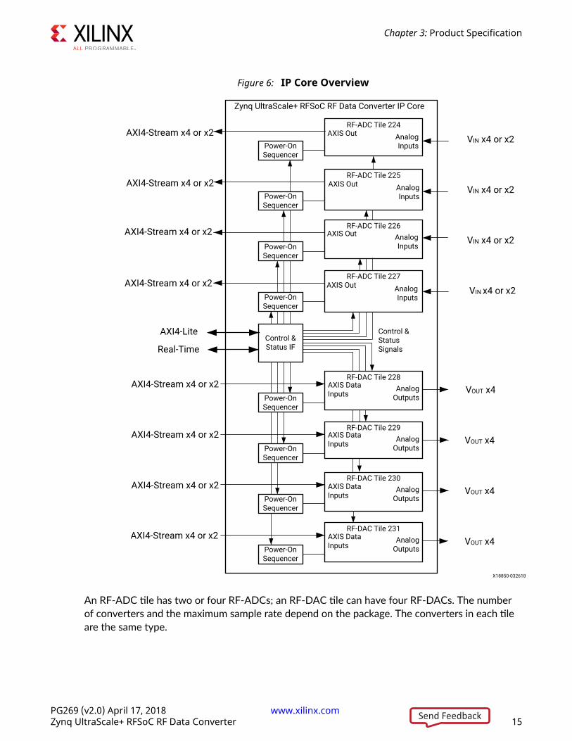
Figure 6: IP Core Overview
RF-ADC Tile 224
Zynq UltraScale+ RFSoC RF Data Converter IP Core
AXIS Out Analog InputsPower-On
Sequencer
RF-ADC Tile 225
Power-OnSequencer
RF-ADC Tile 226
Power-OnSequencer
RF-ADC Tile 227
Power-OnSequencer
Control & Status IF
RF-DAC Tile 228Analog
Outputs
AXIS Data InputsPower-On
Sequencer
RF-DAC Tile 229Analog
Outputs
AXIS Data InputsPower-On
Sequencer
RF-DAC Tile 230Analog
OutputsAXIS Data InputsPower-On
Sequencer
RF-DAC Tile 231Analog
OutputsAXIS Data InputsPower-On
Sequencer
Control & Status Signals
AXI4-Lite
VIN x4 or x2
VIN x4 or x2
VIN x4 or x2
VIN x4 or x2
AXI4-Stream x4 or x2
AXI4-Stream x4 or x2
AXI4-Stream x4 or x2
AXI4-Stream x4 or x2
VOUT x4
VOUT x4
VOUT x4
VOUT x4
AXI4-Stream x4 or x2
AXI4-Stream x4 or x2
AXI4-Stream x4 or x2
AXI4-Stream x4 or x2
AXIS Out Analog Inputs
AXIS Out Analog Inputs
AXIS Out Analog Inputs
Real-Time
X18850-032618
An RF-ADC tile has two or four RF-ADCs; an RF-DAC tile can have four RF-DACs. The numberof converters and the maximum sample rate depend on the package. The converters in each tileare the same type.
Chapter 3: Product Specification
PG269 (v2.0) April 17, 2018 www.xilinx.com [placeholder text]Zynq UltraScale+ RFSoC RF Data Converter 15Send Feedback

PerformanceTo see the performance of the RF-ADC and RF-DAC blocks, see the Zynq UltraScale+ RFSoC DataSheet: DC and AC Switching Characteristics (DS926).
Maximum Frequencies
The s_axi_aclk is limited to between 10 MHz and 200 MHz. All other maximum clockfrequencies are per the Zynq UltraScale+ RFSoC Data Sheet: DC and AC Switching Characteristics(DS926).
Latency
No latency is added by the core. See the Zynq UltraScale+ RFSoC Data Sheet: DC and AC SwitchingCharacteristics (DS926) for latencies through the RF-DAC and RF-ADC.
Related InformationClocking
Resource UseFor full details about performance and resource utilization, visit the Performance and ResourceUtilization web page (registration required).
Port DescriptionsConfiguration Interface PortsTable 1: Configuration Interface Ports
Port Name I/O Clock Descriptions_axi_aclk In N/A AXI clock input. This is a continuous clock.
s_axi_aresetn In N/A Asynchronous reset for the aclk domain
s_axi_awaddr[17:0] In s_axi_aclk Write Address
s_axi_awvalid In s_axi_aclk Write Address Valid
s_axi_awready Out s_axi_aclk Write Address Ready
s_axi_wdata[31:0] In s_axi_aclk Write Data
Chapter 3: Product Specification
PG269 (v2.0) April 17, 2018 www.xilinx.com [placeholder text]Zynq UltraScale+ RFSoC RF Data Converter 16Send Feedback

Table 1: Configuration Interface Ports (cont'd)
Port Name I/O Clock Descriptions_axi_wstrb[3:0] In s_axi_aclk Write Data Byte Strobe
s_axi_wvalid In s_axi_aclk Write Data Valid
s_axi_wready Out s_axi_aclk Write Data Ready
s_axi_bresp[1:0] Out s_axi_aclk Write Response
s_axi_bvalid Out s_axi_aclk Write Response Valid
s_axi_bready In s_axi_aclk Write Response Ready
s_axi_araddr[17:0] In s_axi_aclk Read Address
s_axi_arvalid In s_axi_aclk Read Address Valid
s_axi_arready Out s_axi_aclk Read Address Ready
s_axi_rdata[31:0] Out s_axi_aclk Read Data
s_axi_rresp[1:0] Out s_axi_aclk Read Response
s_axi_rvalid Out s_axi_aclk Read Data Valid
s_axi_rready In s_axi_aclk Read Data Ready
irq Out s_axi_aclk Interrupt output
Multi Converter Synchronization PortsTable 2: Multi Converter Synchronization Ports
Port Name I/O Clock Description1
sysref_in_p In N/A External analog SYSREF input
sysref_in_n In N/A External analog SYSREF input
user_sysref_adc In m0_axis_aclk RF-ADC SYSREF input from programmable logic(PL)/ user design; synchronous to RF-ADC tile 0 PLclock
user_sysref_dac In s0_axis_aclk RF-DAC SYSREF input from programmable logic(PL)/user design; synchronous to RF-DAC tile 0 PLclock
Notes:
1. Please see Multi-converter synchronization section in the aplications sub-section for more information.
Clock Ports Common to RF-DAC TileTable 3: Clock Ports Common to RF-DAC Tile
Port Name1 I/O Clock Description
dacX_clk_p In N/A RF-DAC on-chip PLL reference clock or samplingclock input
dacX_clk_n In N/A RF-DAC on-chip PLL reference clock or samplingclock input
Chapter 3: Product Specification
PG269 (v2.0) April 17, 2018 www.xilinx.com [placeholder text]Zynq UltraScale+ RFSoC RF Data Converter 17Send Feedback

Table 3: Clock Ports Common to RF-DAC Tile (cont'd)
Port Name1 I/O Clock Descriptionclk_dacX Out N/A Output clock to user logic
Notes:
1. X refers to the location of the tile in the converter column.
AXI4-Stream Input Ports for RF-DACsTable 4: AXI4-Stream Input Ports for RF-DACs
Port Name1 I/O Clock DescriptionsX_axis_aclk In N/A Clock input for RF-DAC data input
sXY_axis_aresetn In N/A Synchronous reset for the sX_axis_aclk domain.This should be held low until sX_axis_aclk is stable.
sXY_axis_tdata[M:0] In sX_axis_aclk AXI4-Stream data input
sXY_axis_tvalid In sX_axis_aclk AXI4-Stream valid
sXY_axis_tready Out sX_axis_aclk AXI4-Stream ready
voutXZ_p Out N/A Analog output
voutXZ_n Out N/A Analog output
Notes:
1. X refers to the location of the tile in the converter column. Y refers to the location of the DUC block in the tile (0 to 3).Z refers to the location of the RF-DAC in the tile (0 to 3). M is the number of samples per AXI4-Stream word * 16 forconverter XY.
Real-Time Signal Interface Ports for RF-DACsTable 5: Real-Time Signal Interface Ports for RF-DACs
Port Name1 I/O Clock Description
dacXZ_fast_shutdown[2:0] In N/A
RF-DAC fast shutdown001 - Scale output data by 0.5011 - Scale output data by 0.25111 - Scale output data by 0Others - Normal operation
dacXY_pl_event In clk_dacXRF-DAC PL eventAssert to update RF-DAC settings from the PL
Notes:
1. X refers to the location of the tile in the converter column. Y refers to the location of the DUC block in the tile (0 to 3).Z refers to the location of the RF-DAC in the tile (0 to 3).
Chapter 3: Product Specification
PG269 (v2.0) April 17, 2018 www.xilinx.com [placeholder text]Zynq UltraScale+ RFSoC RF Data Converter 18Send Feedback

Clock Ports Common to RF-ADC TileTable 6: Clock Ports Common to RF-ADC Tile
Port Name1 I/O Clock Description
adcX_clk_p In N/A RF-ADC on-chip PLL reference clock or samplingclock input
adcX_clk_n In N/A RF-ADC on-chip PLL reference clock or samplingclock input
clk_adcX Out N/A Output clock to user logic
Notes:
1. X refers to the location of the tile in the converter column.
AXI4-Stream Input Ports for RF-ADCsTable 7: AXI4-Stream Input Ports for RF-ADCs
Port Name1 I/O Clock DescriptionmX_axis_aclk In N/A Clock input for RF-ADC data output
mXY_axis_aresetn In N/A Synchronous reset for the sX_axis_aclk domain.This should be held low until mX_axis_aclk is stable.
mXY_axis_tdata[M:0] Out mX_axis_aclk AXI4-Stream data output
mXY_axis_tvalid Out mX_axis_aclk AXI4-Stream valid
mXY_axis_tready In mX_axis_aclk AXI4-Stream ready
2 GSPSvinXZ_p In N/A Analog input
vinXZ_n In N/A Analog input
4 GSPSvinX_ZZ_p In N/A Analog input
vinX_ZZ_n In N/A Analog input
Notes:
1. X refers to the location of the tile in the converter column. Y refers to the location of the DDC block in the tile (0 to 3).In 2 GSPS devices, Z refers to the location of the RF-ADC in the tile (0 to 3). In 4 GSPS devices, ZZ is either 01 (the lowerRF-ADC in the tile) or 23 (the upper RF-ADC in the tile). M is the number of samples per AXI4-Stream word * 16 forconverter XY.
Real-Time Signal Interface Ports for 2 GSPS RF-ADCsTable 8: Real-Time Signal Interface Ports for 2 GSPS RF-ADCs
Port Name1,2 I/O Clock Description
adcXY_pl_event In clk_adcXRF-ADC PL eventAssert to update RF-ADC settings from the PL
Chapter 3: Product Specification
PG269 (v2.0) April 17, 2018 www.xilinx.com [placeholder text]Zynq UltraScale+ RFSoC RF Data Converter 19Send Feedback

Table 8: Real-Time Signal Interface Ports for 2 GSPS RF-ADCs (cont'd)
Port Name1,2 I/O Clock Description
adcXZ_over_range Out AsyncOver range output. A High on this output indicatesthat the signal exceeds the full-scale input of theRF-ADC.
adcXZ_over_threshold1 Out mX_axis_aclkOver threshold1 outputSignal amplitude level is above programmablethreshold 1
adcXZ_over_threshold2 Out mX_axis_aclkOver threshold2 outputSignal amplitude level is above programmablethreshold 2
adcXZ_over_voltage Out AsyncOver voltage outputAn Over Voltage condition occurs when a signal farexceeds the normal operating input-range.
Notes:
1. X refers to the location of the tile in the converter column. Y refers to the location of the DDC block in the tile (0 to 3).Z refers to the location of the RF-ADC in the tile (0 to 3).
2. See RF-ADC Threshold and Over Range Settings for details on the real-time signals.
Related InformationRF-ADC Threshold and Over Range Settings
Real-Time Signal Interface Ports for 4 GSPS RF-ADCsTable 9: Real-Time Signal Interface Ports for 4 GSPS RF-ADCs
Port Name1,2 I/O Clock Description
adcXY_pl_event In clk_adcXRF-ADC PL eventAssert to update RF-ADC settings from the PL
adcX_ZZ_over_range Out AsyncOver range output. A High on this output indicatesthat the signal exceeds the full-scale input of theRF-ADC.
adcX_ZZ_over_threshold1 Out mX_axis_aclkOver threshold1 outputSignal amplitude level is above programmablethreshold 1
adcX_ZZ_over_threshold2 Out mX_axis_aclkOver threshold2 outputSignal amplitude level is above programmablethreshold 2
adcX_ZZ_over_voltage Out AsyncOver voltage outputAn Over Voltage condition occurs when a signal farexceeds the normal operating input-range.
Notes:
1. X refers to the location of the tile in the converter column. Y refers to the location of the DDC block in the tile (0 to 3).ZZ is either 01 (the lower RF-ADC in the tile) or 23 (the upper RF-ADC in the tile)
2. See RF-ADC Threshold and Over Range Settings for details on the real-time signals.
Chapter 3: Product Specification
PG269 (v2.0) April 17, 2018 www.xilinx.com [placeholder text]Zynq UltraScale+ RFSoC RF Data Converter 20Send Feedback

Related InformationRF-ADC Threshold and Over Range Settings
Calibration Freeze Ports for 2 GSPS RF-ADCsTable 10: Calibration Freeze Ports for 2 GSPS RF-ADCs
Port Name1 I/O Clock DescriptionadcXY_int_cal_freeze In s_axi_aclk Signal from the PL to indicate that IP should freeze
the calibration. This is typically asserted when theRF-ADC output is below a certain threshold.
adcXY_cal_frozen Out s_axi_aclk Asserted when the calibration is frozen.
Notes:
1. X refers to the location of the tile in the converter column. Y refers to the converter location in the tile (0 to 3).
Calibration Freeze Ports for 4 GSPS RF-ADCsTable 11: Calibration Freeze Ports for 4 GSPS RF-ADCs
Port Name1 I/O Clock DescriptionadcX_ZZ_int_cal_freeze In s_axi_aclk Signal from the PL to indicate that IP should freeze
the calibration. This is typically asserted when theRF-ADC output is below a certain threshold.
adcX_ZZ_cal_frozen Out s_axi_aclk Asserted when the calibration is frozen.
Notes:
1. X refers to the location of the tile in the converter column. ZZ is either 01 (the lower RF-ADC in the tile) or 23 (theupper RF-ADC in the tile).
Register SpaceThe address map, shown in the following table, is split on a per-tile basis. All banks are 8 KB. Thefirst bank contains the functions common to all tiles. Each tile has a bank for control and status.
Table 12: Address Space
AXI4-Lite Address Range ADDR[17:0] Function0x00000 - 0x03FFF IP Common Control and Status
0x04000 - 0x07FFF RF-DAC Tile 0 registers (Tile <n> Registers)
0x08000 - 0x0BFFF RF-DAC Tile 1 registers (Tile <n> Registers)
0x0C000 - 0x0FFFF RF-DAC Tile 2 registers (Tile <n> Registers)
Chapter 3: Product Specification
PG269 (v2.0) April 17, 2018 www.xilinx.com [placeholder text]Zynq UltraScale+ RFSoC RF Data Converter 21Send Feedback

Table 12: Address Space (cont'd)
AXI4-Lite Address Range ADDR[17:0] Function0x10000 - 0x13FFF RF-DAC Tile 3 registers (Tile <n> Registers)
0x14000 - 0x17FFF RF-ADC Tile 0 registers (Tile <n> Registers)
0x18000 - 0x1BFFF RF-ADC Tile 1 registers (Tile <n> Registers)
0x1C000 - 0x1FFFF RF-ADC Tile 2 registers (Tile <n> Registers)
0x20000 - 0x23FFF RF-ADC Tile 3 registers (Tile <n> Registers)
0x24000 - 0x3FFFF Reserved
IP Common Control and StatusTable 13: IP Common Control and Status
Address Range ADDR[13:0] Function0x0000 IP Versioning Information
0x0004 Master Reset Register
0x0100 Common Interrupt Status Register
0x0104 Common Interrupt Enable Register
IP Version Information (0x0000)Table 14: IP Version Information (0x0000)
Bit DefaultValue
AccessType Description
31:24 02
RO
Major
23:16 00 Minor
15:8 00 Revision
7:0 00 Reserved
Master Reset Register (0x0004)Table 15: Master Reset Register (0x0004)
Bit DefaultValue
AccessType Description
31:1 - - Reserved
Chapter 3: Product Specification
PG269 (v2.0) April 17, 2018 www.xilinx.com [placeholder text]Zynq UltraScale+ RFSoC RF Data Converter 22Send Feedback

Table 15: Master Reset Register (0x0004) (cont'd)
Bit DefaultValue
AccessType Description
0 0 R/W AutoClear
Reset All Tiles. Write 1 to this bit to reset all logic in the core and restart thepower-on sequence of all converters in the core.Each converter is configured as per the settings chosen during core generation.The AXI4-Lite registers are unaffected by this reset with the exception of bits 15:8in the Reset State Register for each tile which is set to 0 automatically. The endstate (bits 7:0) is not affected by this reset so the power-up sequence for each tilestarts from state 0 and runs to the value programmed in bits 7:0 of the RestartState register for each tile (the default end state is 0x0F).
Related InformationRestart State Register (0x0008)
Common Interrupt Status Register (0x0100)Table 16: Common Interrupt Status Register (0x0100)
Bit DefaultValue
AccessType Description
31 0 RO, Clearon Read AXI timeout interrupt
30:8 -
RO
Reserved (read 0)
7 0 RF-ADC Tile 3 interrupt
6 RF-ADC Tile 2 interrupt
5 RF-ADC Tile 1 interrupt
4 RF-ADC Tile 0 interrupt
3 RF-DAC Tile 3 interrupt
2 0 RF-DAC Tile 2 interrupt
1 0 RF-DAC Tile 1 interrupt
0 0 RF-DAC Tile 0 interrupt
Chapter 3: Product Specification
PG269 (v2.0) April 17, 2018 www.xilinx.com [placeholder text]Zynq UltraScale+ RFSoC RF Data Converter 23Send Feedback

Common Interrupt Enable Register (0x0104)Table 17: Common Interrupt Enable Register (0x0104)
Bit DefaultValue
AccessType Description
31 0
R/W
AXI timeout interrupt enable
30:8 - Reserved
7 0 RF-ADC Tile 3 interrupt enable
6 0 RF-ADC Tile 2 interrupt enable
5 0 RF-ADC Tile 1 interrupt enable
4 0 RF-ADC Tile 0 interrupt enable
3 0 RF-DAC Tile 3 interrupt enable
2 0 RF-DAC Tile 2 interrupt enable
1 0 RF-DAC Tile 1 interrupt enable
0 0 RF-DAC Tile 0 interrupt enable
Tile <n> RegistersDo not attempt to write to any tile specific registers while the power-on state machine isoperating. To ensure the power-on state machine is not running prior to any register access, pollthe Restart Power-On State Machine register (for tile <n>) and wait for it to read all zeros.
Table 18: Tile <n> Registers
ADDR[12:0] Function0x0000 Reserved
0x0004 Restart Power-On State Machine Register
0x0008 Restart State Register
0x000C Current State Register
0x0010 - 0x00FC Reserved
0x0100 Post-Implementation Simulation Speedup Register
0x0104 - 0x01FC Reserved
0x0200 Interrupt Status Register
0x0204 Interrupt Enable Register
0x0208 Converter 0 Interrupt Register
0x020C Converter 0 Interrupt Enable Register
0x0210 Converter 1 Interrupt Register
0x0214 Converter 1 Interrupt Enable Register
0x0218 Converter 2 Interrupt Register1
0x021C Converter 2 Interrupt Enable Register1
0x0220 Converter 3 Interrupt Register1
Chapter 3: Product Specification
PG269 (v2.0) April 17, 2018 www.xilinx.com [placeholder text]Zynq UltraScale+ RFSoC RF Data Converter 24Send Feedback

Table 18: Tile <n> Registers (cont'd)
ADDR[12:0] Function0x0224 Converter 3 Interrupt Enable Register1
0x0228 RF-DAC/RF-ADC Tile <n> Common Status Register
0x022C Reserved
0x0230 RF-DAC/RF-ADC Tile <n> Disable Register
0x0234-0x3FFF Reserved
Notes:
1. Converter 2 and 3 registers are not applicable for tiles with 4 GS/s RF-ADCs.
Restart Power-On State Machine Register (0x0004)Table 19: Restart Power-On State Machine Register (0x0004)
Bit DefaultValue
AccessType Description
31:1 - - Reserved
0 0 R/W AutoClear
Write 1 to this bit to start the power-on state machine. The state machine startsand stops at the stages programmed in the Restart State Register. This bit staysHigh until the state machine has reached the chosen end state.
Related InformationRestart State Register (0x0008)
Restart State Register (0x0008)Table 20: Restart State Register (0x0008)
Bit DefaultValue
AccessType Description
31:16 - - Reserved
15:8 00 R/W Start Enabled tiles only. Start and End states for the power-on sequence.The default start state of 0x00 and end state of 0x0F should beused to enable the converters and a start state of 0x00 and an endstate of 0x03 should be used to stop the converters. When a 1 iswritten to the bit in the Restart Power-on State Machine Registerfor tile<n>, the power-on state machine is started from the startstate and runs to the end of the end state specified in this register.See Power-up Sequence for details about restarting and power-down.
7:0 0F R/W End
Related InformationPower-up Sequence
Chapter 3: Product Specification
PG269 (v2.0) April 17, 2018 www.xilinx.com [placeholder text]Zynq UltraScale+ RFSoC RF Data Converter 25Send Feedback

Current State Register (0x000C)Table 21: Current State Register (0x000C)
Bit DefaultValue
AccessType Description
31:8 - - Reserved
7:0 00 RO Current state of Power-on state machine. See Power-on Sequence Steps.
Related InformationPower-on Sequence Steps
Post-Implementation Simulation Speedup Register(0x0100)Table 22: Post-Implementation Simulation Speedup Register (0x0100)
Bit DefaultValue
AccessType Description
31:1 - - Reserved
0 0 RW Simulation speed-up for post-implementation simulations. Set High to speed uppost-implementation simulations. This register must not be set in hardware.
Interrupt Status Register (0x0200)Table 23: Interrupt Status Register (0x0200)
Bit DefaultValue
AccessType Description
31:4 - - Reserved (read back 0)
3 0
RO
Converter 3 interrupt bit
2 0 Converter 2 interrupt bit
1 0 Converter 1 interrupt bit
0 0 Converter 0 interrupt bit
Interrupt Enable Register (0x0204)Table 24: Interrupt Enable Register (0x0204)
Bit DefaultValue
AccessType Description
31:4 - - Reserved Enable Read back 0
Chapter 3: Product Specification
PG269 (v2.0) April 17, 2018 www.xilinx.com [placeholder text]Zynq UltraScale+ RFSoC RF Data Converter 26Send Feedback

Table 24: Interrupt Enable Register (0x0204) (cont'd)
Bit DefaultValue
AccessType Description
3 1
R/W
Converter 3 interrupt enable bit
2 1 Converter 2 interrupt enable bit
1 1 Converter 1 interrupt enable bit
0 1 Converter 0 interrupt enable bit
Converter 0 Interrupt Register (0x0208)
Bit DefaultValue
AccessType Description
31:16 - - Reserved Enable Read back 0
15 0 RO Clear onReset
Flags a FIFO overflow in converter when High
14 0 Flags a datapath overflow in converter when High1
13:4 - - Reserved (read back 0)
3 0 RO Clear onReset Flags an Over Range interrupt in converter2
2 0 RO Clear onRead Flags an Over Voltage interrupt in converter2
1:0 N/A Reserved (read back 0)
Notes:
1. A datapath overflow indicates one of the following conditions has occurred:
• Interpolation filter overflow in the RF-DAC• Decimation filter overflow in the RF-ADC• Overflow in the Quadrature Modulation Correction block• Overflow in the RF-DAC Inverse Sinc filter
2. RF-ADC only.
Converter 0 Interrupt Enable Register (0x020C)Table 25: Converter 0 Interrupt Enable Register (0x020C)
Bit DefaultValue
AccessType Description
31:16 - - Reserved (read back 0)
15 1R/W
Enable FIFO overflow interrupt in converter
14 1 Enable datapath overflow interrupt in converter
13:4 - - Reserved (read back 0)
3 1R/W
Enable Over Range interrupt in converter1
2 1 Enable Over Voltage interrupt in converter1
Chapter 3: Product Specification
PG269 (v2.0) April 17, 2018 www.xilinx.com [placeholder text]Zynq UltraScale+ RFSoC RF Data Converter 27Send Feedback

Table 25: Converter 0 Interrupt Enable Register (0x020C) (cont'd)
Bit DefaultValue
AccessType Description
1:0 - - Reserved (read back 0)
Notes:
1. RF-ADC only.
Converter 1 Interrupt Register (0x0210)Table 26: Converter 1 Interrupt Register (0x0210)
Bit DefaultValue
AccessType Description
31:16 - - Reserved (read back 0)
15 0 RO Clear onReset
Flags a FIFO overflow in converter when High
14 0 Flags a datapath overflow in converter when High
13:4 - - Reserved (read back 0)
3 0 RO Clear onReset Flags an Over Range interrupt in converter1
2 0 RO Clear onRead Flags an Over Voltage interrupt in converter1
1:0 - - Reserved (read back 0)
Notes:
1. RF-ADC only.
Converter 1 Interrupt Enable Register (0x0214)Table 27: Converter 1 Interrupt Enable Register (0x0214)
Bit DefaultValue
AccessType Description
31:16 - - Reserved (read back 0)
15 1R/W
Enable FIFO overflow interrupt in converter
14 1 Enable datapath overflow interrupt in converter
13:4 - - Reserved (read back 0)
3 1R/W
Enable Over Range interrupt in converter1
2 1 Enable Over Voltage interrupt in converter1
1:0 - - Reserved (read back 0)
Notes:
1. RF-ADC only.
Chapter 3: Product Specification
PG269 (v2.0) April 17, 2018 www.xilinx.com [placeholder text]Zynq UltraScale+ RFSoC RF Data Converter 28Send Feedback

Converter 2 Interrupt Register (0x0218)Table 28: Converter 2 Interrupt Register (0x0218)
Bit DefaultValue
AccessType Description
31:16 - - Reserved (read back 0)
15 0 RO Clear onReset
Flags a FIFO overflow in converter when High
14 0 Flags a datapath overflow in converter when High
13:4 - - Reserved (read back 0)
3 0 RO Clear onReset Flags an Over Range interrupt in converter1
2 0 RO Clear onRead Flags an Over Voltage interrupt in converter1
1:0 - - Reserved (read back 0)
Notes:
1. RF-ADC only.
Converter 2 Interrupt Enable Register (0x021C)Table 29: Converter 2 Interrupt Enable Register (0x021C)
Bit DefaultValue
AccessType Description
31:16 - - Reserved (read back 0)
15 1R/W
Enable FIFO overflow interrupt in converter
14 1 Enable datapath overflow interrupt in converter
13:4 - - Reserved (read back 0)
3 1R/W
Enable Over Range interrupt in converter1
2 1 Enable Over Voltage interrupt in converter1
1:0 - - Reserved (read back 0)
Notes:
1. RF-ADC only.
Converter 3 Interrupt Register (0x0220)Table 30: Converter 3 Interrupt Register (0x0220)
Bit DefaultValue
AccessType Description
31:16 - - Reserved (read back 0)
Chapter 3: Product Specification
PG269 (v2.0) April 17, 2018 www.xilinx.com [placeholder text]Zynq UltraScale+ RFSoC RF Data Converter 29Send Feedback

Table 30: Converter 3 Interrupt Register (0x0220) (cont'd)
Bit DefaultValue
AccessType Description
15 0 RO Clear onReset
Flags a FIFO overflow in converter when High
14 0 Flags a datapath overflow in converter when High
13:4 - - Reserved (read back 0)
3 0 RO Clear onReset Flags an Over Range interrupt in converter1
2 0 RO Clear onRead Flags an Over Voltage interrupt in converter1
1:0 - - Reserved (read back 0)
Notes:
1. RF-ADC only.
Converter 3 Interrupt Enable Register (0x0224)Table 31: Converter 3 Interrupt Enable Register (0x0224)
Bit DefaultValue
AccessType Description
31:16 - - Reserved (read back 0)
15 1R/W
Enable FIFO overflow interrupt in Converter
14 1 Enable datapath overflow interrupt in Converter
13:4 - - Reserved (read back 0)
3 1R/W
Enable Over Range interrupt in converter1
2 1 Enable Over Voltage interrupt in converter1
1:0 - - Reserved (read back 0)
Notes:
1. RF-ADC only.
Chapter 3: Product Specification
PG269 (v2.0) April 17, 2018 www.xilinx.com [placeholder text]Zynq UltraScale+ RFSoC RF Data Converter 30Send Feedback

RF-DAC/RF-ADC Tile <n> Common Status Register(0x0228)Table 32: RF-DAC/RF-ADC Tile <n> Common Status Register (0x0228)
Bit DefaultValue
AccessType Description1,2
31:4
- RO
Reserved
3 PLL locked. Asserted when the tile PLL has achieved lock.
2 Power-up state. Asserted when the tile is in operation.
1 Supplies up. Asserted when the external supplies to the tile are stable.
0 Clock present. Asserted when the reference clock for the tile is present.
Notes:
1. <n> is 0 to 3.2. See Register Space for register <n> address.
Related InformationRegister Space
RF-DAC/RF-ADC Tile <n> FIFO Disable Register(0x0230)Table 33: RF-DAC/RF-ADC Tile <n> FIFO Disable Register (0x0230)
Bit DefaultValue
AccessType Description1,2
31:1 - - Reserved
0 0 R/W Disable the interface FIFO for converter <n>
Notes:
1. <n> is 0 to 32. See Register Space for register <n> address.
Related InformationRegister Space
Chapter 3: Product Specification
PG269 (v2.0) April 17, 2018 www.xilinx.com [placeholder text]Zynq UltraScale+ RFSoC RF Data Converter 31Send Feedback

Chapter 4
Designing with the CoreThe RF Data Converter solution consists of the Zynq® UltraScale+™ RFSoC RF Data Converter IPcore configuration in the Vivado® Integrated Design Environment (IDE) and the RF dataconverter (RFdc) driver Application Programming Interface (API).
IP Core Configuration in Vivado DesignSuiteThe Zynq® UltraScale+™ RFSoC RF Data Converter IP core configuration screen in the Vivado®
IDE sets up the physical configuration of the RF-ADCs and RF-DACs in the RFSoC. Theconfiguration screen is used to enable tiles, configure decimation, interpolation, and mixing, setup converter sample rates, the Programmable Logic (PL) interface word widths and data types,and enables the optional interface ports. The IP core also handles the configuration and power-up of the data converters. This ensures that the settings specified in the Vivado IDE are appliedto the RF-ADCs and RF-DACs immediately after the PL configuration completes.
Software DriverThe RFdc driver API provides runtime interaction and monitoring of the data converters. Thisincludes responding to interrupts, changing some settings, such as mixer frequency, and alsointeracting with the IP core to power up or down RF-ADC or RF-DAC tiles. The RFdc driver APIis available as a bare-metal or Linux driver validated on both MicroBlaze™ and RFSoC ProcessingSystem (PS) APU or RPU processors.
RF-ADCEvery RF-ADC in a tile has its own dedicated high-performance input buffer and includesfeatures optimized for direct conversion applications including quadrature modulator correction(QMC), full complex mixers, and decimation filters.
Chapter 4: Designing with the Core
PG269 (v2.0) April 17, 2018 www.xilinx.com [placeholder text]Zynq UltraScale+ RFSoC RF Data Converter 32Send Feedback

Figure 7: RF-ADC Functionality Block Diagram (Simplified)
ADCVIN0_NVIN0_P DATA_ADC0[127:0]
STATUS_ADC0[15:0]
CONTROL_ADC0[15:0]
Threshold Detect
I Decimation
Q DecimationG
earboxFIFO
QMCGain/Phase
Crossbar
I and Q Mixer
X18254-091117
Certain functions can only be executed when the RF-ADCs in a tile are paired. The even-numbered RF-ADCs are used for I datapaths and the odd-numbered RF-ADCs are used for Qdatapaths. All of the available built-in functionality of a tile and each of the RF-ADCs within a tileare configured with the supporting RFdc driver API and/or core configuration screen in theVivado® IDE.
Related InformationQuadrature Modulator Correction
RF-ADC Analog InputEvery RF-ADC in a tile has its own differential analog input buffer. This input is optimized forperformance and requires source impedance matching for best dynamic performance.
Figure 8: RF-ADC Analog Input
packagedie
ADCPair
12 bits 50 Ω 50 Ω
BUFDigital
GND
VCCINT_AMS (0.85) ADC_AVCCAUX (1.8V)
VP
VN
VCM1.2V
ADC_GND
ADC_AVCC (0.925V)
Z0=100 Ω
Vin
250 mV
VP-VN = 1V pk-pk
VCM1.2V
X19533-040518
There are several ways to drive an RF-ADC in a tile. Driving the RF-ADC can be either active orpassive. However, optimum performance is achieved by driving the analog input differentially.Using a differential amplifier, AC or DC coupled, to drive the RF-ADC provides a flexible interfacewith excellent performance. For AC coupled mode, the input signals should be AC coupled inusing capacitors. For DC coupled mode, the output VCM buffer is enabled as shown in the figureabove. This buffer is only enabled when DC coupled mode is selected. This VCM buffer allows
Chapter 4: Designing with the Core
PG269 (v2.0) April 17, 2018 www.xilinx.com [placeholder text]Zynq UltraScale+ RFSoC RF Data Converter 33Send Feedback

the user to align the common mode of the external active driving circuit with the ADC internalcommon requirements. Two VCM buffers (VCM01,VCM23) are available for each tile. For allapplications where the signal-to-noise ratio (SNR) is a key parameter, Xilinx recommends using adifferential transformer or balun configuration. See the UltraScale Architecture PCB Design UserGuide (UG583) for details on how to design the input networks and PCB.
RF-ADC Digital DatapathAn RF-ADC component in a tile has integrated DSP features which can be enabled by the user topre-process the sampled data from the RF-ADC device before it is passed to the PL. The differentDSP function blocks are as follows:
• Detection functionality—containing a dual level programmable threshold that provides twoflags to the internal interconnect logic, and is asserted when the absolute value of the RF-ADC is greater or smaller than the programmed threshold values.
• Compensation functionality—containing a quadrature modulator correction (QMC) block witha coarse delay adjustment block
• Digital down converter (DDC)—consists of mixing followed by decimation
• Mixer—coarse (quarter and half rate) and fine (NCO with 48-bit frequency resolution)
• Signal decimation functionality—decimation by 2, 4, or 8 is supported
Single, multiple, or all DSP functions can be used or bypassed. Some functions, such as the QMC,require activation of the same function in both I and Q RF-ADCs. Even numbered RF-ADCs arealways used for I datapaths, and odd numbered RF-ADCs are used for Q datapaths. You canimplement, configure, or modify the functionality of one or multiple functions using the IP core.The following figure shows the available functions in an RF-ADC and the functions are describedin this section.
Chapter 4: Designing with the Core
PG269 (v2.0) April 17, 2018 www.xilinx.com [placeholder text]Zynq UltraScale+ RFSoC RF Data Converter 34Send Feedback
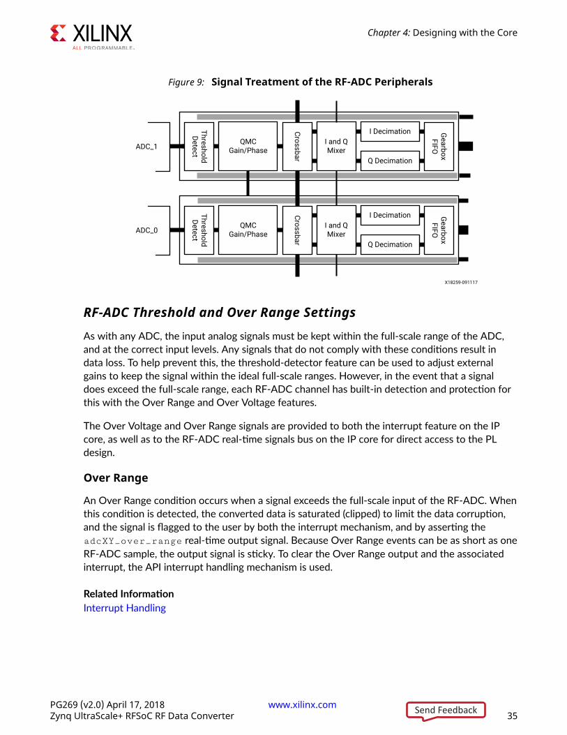
Figure 9: Signal Treatment of the RF-ADC Peripherals
ADC_1HSADC
Threshold Detect
QMCGain/Phase
I Decimation
Q Decimation
GearboxFIFO
I and Q Mixer
ADC_0HSADC
Threshold Detect
QMCGain/Phase
I Decimation
Q Decimation
Gearbox FIFO
CrossbarCrossbar
I and Q Mixer
X18259-091117
RF-ADC Threshold and Over Range Settings
As with any ADC, the input analog signals must be kept within the full-scale range of the ADC,and at the correct input levels. Any signals that do not comply with these conditions result indata loss. To help prevent this, the threshold-detector feature can be used to adjust externalgains to keep the signal within the ideal full-scale ranges. However, in the event that a signaldoes exceed the full-scale range, each RF-ADC channel has built-in detection and protection forthis with the Over Range and Over Voltage features.
The Over Voltage and Over Range signals are provided to both the interrupt feature on the IPcore, as well as to the RF-ADC real-time signals bus on the IP core for direct access to the PLdesign.
Over Range
An Over Range condition occurs when a signal exceeds the full-scale input of the RF-ADC. Whenthis condition is detected, the converted data is saturated (clipped) to limit the data corruption,and the signal is flagged to the user by both the interrupt mechanism, and by asserting theadcXY_over_range real-time output signal. Because Over Range events can be as short as oneRF-ADC sample, the output signal is sticky. To clear the Over Range output and the associatedinterrupt, the API interrupt handling mechanism is used.
Related InformationInterrupt Handling
Chapter 4: Designing with the Core
PG269 (v2.0) April 17, 2018 www.xilinx.com [placeholder text]Zynq UltraScale+ RFSoC RF Data Converter 35Send Feedback

Over Voltage
An Over Voltage condition occurs when a signal far exceeds the normal operating input range.Because an excessive voltage on the inputs can damage the input buffers, an Over Voltage eventresults in the automatic shutdown of the input buffer to protect it. The Over Voltage circuitmonitors each of the signals of the differential inputs independently, and flags the conditionwhen any individual input signal exceeds the maximum input voltage or is less than the minimuminput voltage of the RF-ADC input buffer.
The Over Voltage feature offers protection for signals in the range defined in the Zynq UltraScale+RFSoC Data Sheet: DC and AC Switching Characteristics (DS926). Signals exceeding this maximumare not permitted, and care must be taken externally to ensure that such voltages are notpresented to the RF-ADC inputs.
When an Over Voltage condition is detected the signal is flagged to the user by both theinterrupt mechanism, and by asserting the adcXY_over_voltage real-time output signal. TheOver Voltage real-time output is asserted and deasserted asynchronously, and providesimmediate notification of the event. As a result, the Over Voltage output self-clears when theOver Voltage condition is no longer present. The associated interrupt is sticky, so requiresclearing by the API interrupt handling routines.
After an Over Voltage event, the input buffer automatically re-enables, and the RF-ADC resumesoperation as before. Because the data produced by the RF-ADC must pass through the digitaldatapath, there is a latency of 20 ns + the datapath latency, before valid RF-ADC data isgenerated after the deassertion of the adcXY_over_voltage output.
The following figure illustrates the Threshold, Over Range, and Over Voltage levels and theresponse of these with an increasing input analog signal.
Chapter 4: Designing with the Core
PG269 (v2.0) April 17, 2018 www.xilinx.com [placeholder text]Zynq UltraScale+ RFSoC RF Data Converter 36Send Feedback

Figure 10: Threshold, Over Range, and Over Voltage Levels
2.10V
1.80V
Normal Range
0.00V
-0.30V
Over Range
Over Range
Over Voltage
Over Voltage
Max. voltage rating
Min. voltage rating
Over Range Flag
Over Voltage Flag
Nominal supply voltage
VCMFully
reliable range
Not supported
Not supported
Over Range Flag interrupt
clear
VCM-0.25V
VCM+0.25V
VCM-0.45V
X20472-032118
VCM+0.45V
Related InformationInterrupt Handling
Threshold Settings
Instead of waiting for a signal to propagate through the signal processing blocks, the thresholdfeature provides an early indication of the incoming signal level. This early indication of the signallevel can be used by the automatic gain control (AGC) implemented in the PL. Threshold levelsused to indicate the input signal level are set using the RFdc driver API.
Threshold monitoring occurs when the RF-ADC sampled data enters the datapath. This data iscompared to a user-defined threshold. A threshold status signal is sent to the outputs on the IPcore, to indicate that a user-defined threshold has been exceeded. The outputs are calledadcXY_over_threshold1 and adcXY_over_threshold2. The modes of the thresholdmonitoring circuit are listed in the following table.
Table 34: Threshold Signaling Modes
Mode DescriptionOff The threshold circuit is disabled and the status outputs are Low.
Sticky over The threshold status signal is High when the data from the RF-ADC exceeds the programmedupper threshold value. The status is kept until a clear action is sent.1
Chapter 4: Designing with the Core
PG269 (v2.0) April 17, 2018 www.xilinx.com [placeholder text]Zynq UltraScale+ RFSoC RF Data Converter 37Send Feedback

Table 34: Threshold Signaling Modes (cont'd)
Mode Description
Sticky under
The threshold status signal is High when the data from the RF-ADC remains below theprogrammed lower threshold value for the duration of a user-specified time or delay. The statusis kept until a clear action is sent1. This delay value for the lower threshold is defined by a 32-bitcounter. The counter is set using the RFdc driver API. Using this mechanism prevents shortduration excursions triggering a threshold event.
Hysteresis
The status output is set when the programmed upper threshold value is exceeded, and is clearedwhen the signal remains below the lower threshold value for the duration of a user-specifieddelay value. This delay value for the lower threshold is defined by a 32-bit counter. The counter isset using the RFdc driver API. The delay adds hysteresis to the threshold detection to preventshort duration excursions triggering a threshold event.
Notes:
1. To clear see Clearing Threshold Flags.
Threshold levels are set as 14-bit unsigned values, with any value from 0 to 16383 allowed. Themaximum value, 16383 represents the absolute value of the full-scale input of the RF-ADC. The32-bit programmable delay counts RF-ADC samples. To relate this count to a specific time, thefollowing formulas can be used:
Clearing Threshold Flags
After the threshold values assert in the Sticky Over and Sticky Under modes, the flags can becleared in two ways; by issuing the clear command directly, or by using the AutoClear feature.The AutoClear mode clears the threshold whenever the QMC Gain value associated with thatRF-ADC is updated.
Threshold Operation Example
The following figure illustrates the threshold unit operation. The diagram shows three thresholds,a, b, and c, each configured in a different threshold mode. In hardware all threshold units haveindependent threshold levels and delay values. In this example the threshold levels are indicatedby the dashed horizontal lines, and all units use the same levels for the purpose of illustration.The delay value is set to 5, and the sticky thresholds have been set up to be cleared by differentclear modes. The behavior is described in the following sections.
Chapter 4: Designing with the Core
PG269 (v2.0) April 17, 2018 www.xilinx.com [placeholder text]Zynq UltraScale+ RFSoC RF Data Converter 38Send Feedback
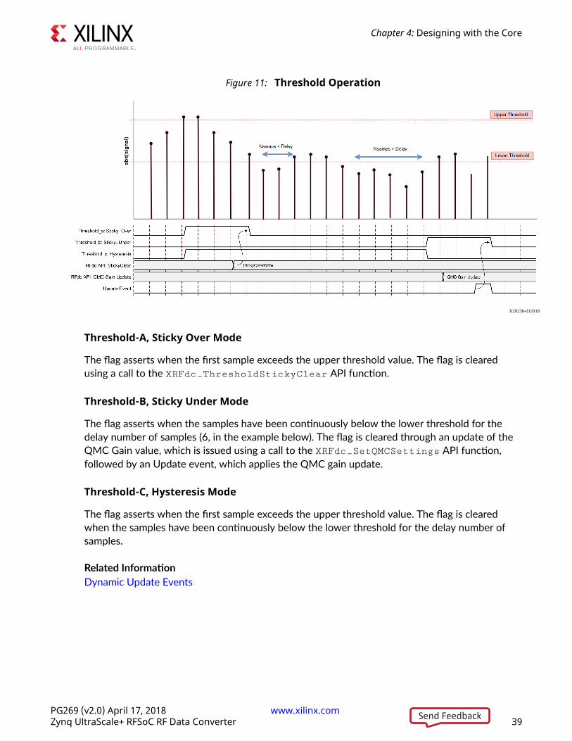
Figure 11: Threshold Operation
X20238-012918
Threshold-A, Sticky Over Mode
The flag asserts when the first sample exceeds the upper threshold value. The flag is clearedusing a call to the XRFdc_ThresholdStickyClear API function.
Threshold-B, Sticky Under Mode
The flag asserts when the samples have been continuously below the lower threshold for thedelay number of samples (6, in the example below). The flag is cleared through an update of theQMC Gain value, which is issued using a call to the XRFdc_SetQMCSettings API function,followed by an Update event, which applies the QMC gain update.
Threshold-C, Hysteresis Mode
The flag asserts when the first sample exceeds the upper threshold value. The flag is clearedwhen the samples have been continuously below the lower threshold for the delay number ofsamples.
Related InformationDynamic Update Events
Chapter 4: Designing with the Core
PG269 (v2.0) April 17, 2018 www.xilinx.com [placeholder text]Zynq UltraScale+ RFSoC RF Data Converter 39Send Feedback
Threshold RFdc Driver API Commands
The threshold levels and delay values are configured using the RFdc driver API.
// Initial Setup
XRFdc_Threshold_Settings Threshold_Settings;Threshold_Settings.UpdateThreshold = XRFDC_UPDATE_THRESHOLD_BOTH; // Setup values for threshold 0 and 1Threshold_Settings.ThresholdMode[0] = XRFDC_TRSHD_STICKY_UNDER; // Set threshold0 mode to Sticky UnderThreshold_Settings.ThresholdUnderVal[0] = 1000; // Measured in 14-bit unsigned LSBsThreshold_Settings.ThresholdAvgVal[0] = 10; // Data must be below lower threshold for 10*8 4 GSPS RF-ADC samples
// Write threshold values to the selected Tile / RF-ADC
XRFdc_SetThresholdSettings(ptr, Tile, Block, &Threshold_Settings);
The threshold clear operation is shown in the following code examples.
• Clear the thresholds by writing directly using the RFdc driver API:
// Initial Setup
XRFdc_SetThresholdClrMode(ptr, Tile, Block, Threshold#, XRFDC_THRESHOLD_CLRMD_MANUAL_CLR);....// During application run-time (after a threshold asserts)
XRFdc_ThresholdStickyClear(ptr, Tile, Block, Threshold#);
• Clear the thresholds using the AutoClear function; the threshold clears with the QMC GainUpdate:
// Initial Setup
XRFdc_QMC_Settings QMC_Settings;XRFdc_SetThresholdClrMode(ptr, Tile, Block, Threshold#, XRFDC_THRESHOLD_CLRMD_AUTO_CLR);....// During application run-time (after a threshold asserts - update t)
QMC_Settings.GainCorrectionFactor = new_gain_value;XRFdc_SetQMCSettings(ptr, XRFDC_ADC_TILE, Tile, Block, &QMC_Settings);...// QMC Gain applied by an Update Event
Chapter 4: Designing with the Core
PG269 (v2.0) April 17, 2018 www.xilinx.com [placeholder text]Zynq UltraScale+ RFSoC RF Data Converter 40Send Feedback
Related InformationXRFdc_SetThresholdSettingsXRFdc_SetThresholdClrModeXRFdc_ThresholdStickyClearXRFdc_SetQMCSettings
Threshold Applications
A common use for threshold detectors is in Automatic Gain Control (AGC) applications.
Related InformationAutomatic Gain Control Systems
Over Range Settings
There are two types of Over Range signals available as status outputs to the programmable logic,Over Voltage and Over Range. The IP core exposes these signals using the interrupt mechanism,so any violation is immediately flagged to the user application. These are triggered when normalor expected operating levels are exceeded.
Over Voltage Signal
An Over Voltage signal is detected whenever the input signal exceeds a safe input range from theRF-ADC input buffers.
Over Range Signal
• When the input signal exceeds the ± digital full-scale range of an RF-ADC, an Over Rangesignal is detected.
• An Over Range signal is measured at the raw digital output of the RF-ADC.
Chapter 4: Designing with the Core
PG269 (v2.0) April 17, 2018 www.xilinx.com [placeholder text]Zynq UltraScale+ RFSoC RF Data Converter 41Send Feedback

RF-ADC Mixer with Numerical Controlled Oscillator
The mixer function has three modes: bypass (no mixing), coarse mixing or fine mixing. Fine mixingautomatically enables the NCO which is used to generate the carrier frequency. The mixersupports full quadrature mixing, with both real to I/Q and I/Q to I/Q modes supported.
Figure 12: RF-ADC Mixer with NCO DSP Block
NCO
Fine Mixer
Coarse MixerN0, Fs/4, Fs/2, or -Fs/4
QIN
IINIOUT
QOUT
3 dB
3 dB
X18261-032318
Coarse Mixer:
• The coarse mixer allows the data to be mixed with a carrier of 0, Fs/2, Fs/4, or –Fs/4.
• Mixing with a 0 carrier bypasses the mixer component.
Fine Mixer:
• The fine mixer allows the data to be shifted up or down in frequency by an arbitrary amount.
• The frequency shift amount is obtained by programming the mixer frequency generated in theNCO. The fine mixer also supports 18-bit phase adjustment.
Chapter 4: Designing with the Core
PG269 (v2.0) April 17, 2018 www.xilinx.com [placeholder text]Zynq UltraScale+ RFSoC RF Data Converter 42Send Feedback

• The NCO phase can be synchronized within a tile using XRFdc_UpdateEvent.
• The NCO phase can be synchronized across tiles using an external event signal (SYSREF orMARKER).
• To manage potential overflow, the fine mixer output includes 3 dBV attenuation, as shown inthe figure above. This attenuation is not relevant in R2C mode, so the automatic modeselection from the API selects the correct attenuation level following the RF-ADC mixerscaling output factor (see the table below). A manual selection is also possible, allowing 0 dBVor -3 dBV.
Table 35: RF-ADC Mixer Scaling Output Factor
Tile Usage Coarse Mixer Auto Fine MixerIQ (C2C) 1 (0 dBV) 0.707 (-3 dBV)
Real (R2C) 1 (0 dBV) 0.997 (~0 dBV)
The mixer settings can be configured in the core, or by using the RFdc driver API. The core isused to set the initial mixer settings (for example, mixer type and mixer mode), and the RFdcdriver API is used to adjust the settings at runtime. Both the RFdc driver API and the corecompute the required register settings based on the supplied sample rates and desiredfrequencies. A sample configuration screen is shown in the following figure. See the RF-ADCConverter Configuration section for information on the settings.
Chapter 4: Designing with the Core
PG269 (v2.0) April 17, 2018 www.xilinx.com [placeholder text]Zynq UltraScale+ RFSoC RF Data Converter 43Send Feedback

Figure 13: RF-ADC Mixer Settings Configuration
Related InformationXRFdc_UpdateEventRF-ADC Converter Configuration
Chapter 4: Designing with the Core
PG269 (v2.0) April 17, 2018 www.xilinx.com [placeholder text]Zynq UltraScale+ RFSoC RF Data Converter 44Send Feedback
RF-ADC Mixer RFdc API Example
Related RFdc driver API functions are shown in the following code. This code illustrates the useof the NCO Phase reset function. This function must be used at startup to initialize the phase ofthe fine mixer to a valid state. Note that the following code resets the NCOs in all tiles.
XRFdc_Mixer_Settings Mixer_Settings;
for(tile=0;tile<4; tile++) // Make sure the mixer settings update use the Tile event for(block=0; block<2; block++) XRFdc_GetMixerSettings (ptr, XRFDC_ADC_TILE, tile, block, &Mixer_Settings); Mixer_Settings.EventSource = XRFDC_EVNT_SRC_TILE; //Mixer Settings are updated with a tile event XRFdc_SetMixerSettings (ptr, XRFDC_ADC_TILE, tile, block, &Mixer_Settings);
// Reset NCO phase of both DDCs in Tile0 (assuming both are active) XRFdc_ResetNCOPhase(ptr, XRFDC_ADC_TILE, tile, 0); // DDC Block0 XRFdc_ResetNCOPhase(ptr, XRFDC_ADC_TILE, tile, 1); // DDC Block1
XRFds_UpdateEvent(ptr, XRFDC_ADC_TILE, tile, 1, XRFDC_EVENT_MIXER); //Generate a Tile Event
Related InformationXRFdc_GetMixerSettingsXRFdc_SetMixerSettingsXRFdc_ResetNCOPhase
RF-ADC Decimation Filters
Decimation filters are required to implement the down-sampling and filtering part of the digital-down conversion (DDC) process. The overall filter response is determined by the number ofdecimation stages used. The decimation chain consists of three FIR filter stages which can becombined to implement variable decimation rates. When a FIR stage is not used it isautomatically powered down. The decimation filters allow for the creation of the following:
• 1x: All filter stages are bypassed
• 2x: Decimation filtering using a single stage
• 4x: Decimation filtering using two stages
• 8x: Decimation filtering using all three available stages
Each decimation filter element has a different number of taps and the stop-band attenuation andripple are shown in Decimation Filter Details. The decimation filter chains can operate on eitherI/Q data or real data. Unused filter chains are powered down.
Chapter 4: Designing with the Core
PG269 (v2.0) April 17, 2018 www.xilinx.com [placeholder text]Zynq UltraScale+ RFSoC RF Data Converter 45Send Feedback

Each of the filter stages can overflow given the step-response of a FIR filter, especially when full-scale data is on the input. To detect and protect the datapath from overflow, each filter stage andsub-phase has a signed overflow status signal and saturation at the output. When a filter stage isnot used, the flag is forced zero. These flags are connected to the datapath interrupt mechanismwhich is described in Interrupt Handling. The multiplexer in the following figure shows thedecimation level selected in the IP configuration with the corresponding selection of decimationfilter blocks.
Figure 14: RF-ADC Decimation Filter
Data InFIR2 FIR1
DataOut
FIR2 FIR1 FIR0
FIR2
X18267-112717
Table 36: Decimation Filter Operating Modes
Mode Description2 GSPS
OFF The entire filter is disabled/powered down (applies when RF-ADC is disabled)
1x The entire filter is bypassed
2x 2x decimation, 80% Nyquist passband1
4x 4x decimation, 80% Nyquist passband
8x 8x decimation, 80% Nyquist passband
4 GSPS
OFF The entire filter is disabled/powered down (applies when RF-ADC is disabled)
1x The entire filter is bypassed
2x 2x decimation, 80% Nyquist passband
4x 4x decimation, 80% Nyquist passband
8x 8x decimation, 80% Nyquist passband
Notes:
1. 80% Nyquist passband is 0.4*Fs
Chapter 4: Designing with the Core
PG269 (v2.0) April 17, 2018 www.xilinx.com [placeholder text]Zynq UltraScale+ RFSoC RF Data Converter 46Send Feedback

Related InformationInterrupt HandlingDecimation Filter Details
Decimation Filter Use
The IP core is used to set the decimation rate. This is set in the Vivado® IDE because changingthe decimation rate directly affects the physical interface as the bandwidth to the PL changes.The filters that are enabled are as shown in the following figure. Enable the RF-ADC by checkingthe Enable ADC checkbox. See RF-ADC Converter Configuration for information on the settings.
Figure 15: RF-ADC Decimation Filter Configuration
Related InformationRF-ADC Converter Configuration
Related API Commands
The RFdc driver API can be used to get the decimation rate set in the IP core using the followingcode.
// Get Decimation factor for Tile0, DDC Block1
int Tile = 0;u32 Block = 1;u32 Decimation_Factor;if( XRFdc_GetDecimationFactor (ptr, Tile, Block, &DecimationFactor) == XST_SUCCESS) xil_printf("ADC Tile%1d,%1d Decimation Factor is: %d", Tile, Block, Decimation_Factor);
Chapter 4: Designing with the Core
PG269 (v2.0) April 17, 2018 www.xilinx.com [placeholder text]Zynq UltraScale+ RFSoC RF Data Converter 47Send Feedback

Decimation Filter Details
The decimation filter chain consists of three FIR filters: FIR2, FIR1 and FIR0, which can beenabled to give successive decimation by a factor of two per stage. The filter transfer functionsare as shown in the following figures.
Figure 16: FIR2 and FIR1 Frequency Response
Figure 17: FIR0 and 2x Decimation Frequency Response
Chapter 4: Designing with the Core
PG269 (v2.0) April 17, 2018 www.xilinx.com [placeholder text]Zynq UltraScale+ RFSoC RF Data Converter 48Send Feedback

Figure 18: 4x Decimation and 8x Decimation Frequency Response
The filter coefficients for the decimation filters are shown in the following tables.
FIR2
1stHalf
5 0 -17 0 44 0 -96 0 187 0 -335 0 565 0 -906
0 1401 0 -2112 0 3145 0 -4723 0 7415 0 -13331 0 41526
CentreTap 65536
2ndHalf
5 0 -17 0 44 0 -96 0 187 0 -335 0 565 0 -906
0 1401 0 -2112 0 3145 0 -4723 0 7415 0 -13331 0 41526
FIR1
1st Half -12 0 84 0 -337 0 1008 0 -2693 0 10142
Centre Tap 16384
2nd Half -12 0 84 0 -337 0 1008 0 -2693 0 10142
FIR0
1st Half -6 0 54 0 -254 0 1230
Centre Tap 2048
2nd Half -6 0 54 0 -254 0 1230
RF-ADC Programmable Logic Data InterfaceThe data interface between the RF-ADC tiles and the PL is implemented using parallel datastreams, using the AXI4-Stream protocol. These data streams are output through the gearboxFIFOs which provide a flexible interface between the user application and the RF-ADC tile. Themaximum interface width is 128 bits per stream, representing up to eight 16-bit big endianwords. The data streams and associated FIFOs have a configurable number of words whichprovide the flexibility to choose between the number of words and clock frequency to interfacewith the PL design. There are four streams per tile, and the naming convention is mXY_axis,where X represents the RF-ADC tile number and Y represents a stream (FIFO) output from thattile. The following figure shows the interfaces.
Chapter 4: Designing with the Core
PG269 (v2.0) April 17, 2018 www.xilinx.com [placeholder text]Zynq UltraScale+ RFSoC RF Data Converter 49Send Feedback

Figure 19: RF-ADC Programmable Logic Data Interface
4 GSPS ADC
Decimation
Decimation
Decimation
Decimation
Mixer/NCO
Mixer/NCO 4 GSPS ADC
m00_axis128-bit
m01_axis128-bit
m02_axis128-bit
m03_axis128-bit
Vin0
Vin1
X19538-032718
Interface Data Formats
The data streams represent real or I/Q data, depending on the RF-ADC tile configuration. For4 GSPS RF-ADC tiles, a given stream is either real, I or Q. If an RF-ADC is configured with I/Qoutput data, then the streams with an even number represent I data and the streams with an oddnumber represent Q data. These 4 GSPS real and I/Q configurations are shown in RF-ADC IPConfiguration .
For 2 GSPS RF-ADC tiles, a given stream is either real or I/Q interleaved. If an RF-ADC isconfigured with I/Q output data, then the even-numbered samples of the stream represent I dataand the odd-numbered samples represent Q data. These 2 GSPS Real and I/Q configurations areillustrated in the following sections.
Related InformationRF-ADC IP Configuration
Interface Data and Clock Rates
The total data rate per channel to the PL is determined by a number of factors, RF-ADC samplerate, decimation factor, and I/Q/Real data formats. The gearbox FIFOs provide a way ofinterfacing this data rate to the clock frequency of the PL design, by allowing the number ofwords per clock to be altered. The only requirements are that the number of words and clockrate combine to match the output data rate of the RF-ADC and the decimation rate, if enabled.All RF-ADCs in a tile share a common interface clock frequency. This is shown by the followingequations, where 2GIQMode is set to 2 for a 2 GSPS RF-ADC tile and I/Q mode is enabled and setto 1 otherwise.
Chapter 4: Designing with the Core
PG269 (v2.0) April 17, 2018 www.xilinx.com [placeholder text]Zynq UltraScale+ RFSoC RF Data Converter 50Send Feedback

The core automatically calculates the data rates based on the RF-ADC sample rate and datapathsettings. This is shown in the following figure. See the RF-ADC Converter Configuration forinformation on the settings.
Figure 20: RF-ADC Interface Data and Clock Rates Configuration
Because each tile has independent clocking, sample rates, clock rates, PL rates, andconfigurations can be specified on a per-tile basis.
Related InformationRF-ADC Converter Configuration
PL Clock Interface
The AXI4-Stream data for all four tile streams is synchronous to a clock from the PL, which has anaming convention of mX_axis_aclk, where X represents the RF-ADC tile number. This clockmust be at the frequency specified by the Required AXI4-Stream clock displayed on the IP coreconfiguration screen.
The RF-ADC tile also outputs a clock that can be used by the PL. This output clock is a dividedversion of the RF-ADC sample clock, and is therefore frequency locked to it. This clock has anaming convention of clk_adcX, where X represents the RF-ADC tile number.
Chapter 4: Designing with the Core
PG269 (v2.0) April 17, 2018 www.xilinx.com [placeholder text]Zynq UltraScale+ RFSoC RF Data Converter 51Send Feedback
Interface FIFO Overflow
The data rate through the interface gearbox FIFOs must be constant during runtime of the RF-ADC tile, with no frequency drift between the PL clock and RF-ADC sample clock domains. Ifthere is a frequency mismatch between these domains, a FIFO overflow might occur. Theinterface FIFOs have a built-in feature to determine if FIFO overflow has occurred, which isflagged to the PL using the IP interrupt mechanism.
There are two types of overflow, actual and marginal. Actual overflow indicates that the FIFOread/write pointers are overlapping, which means data is not being transferred safely betweendomains, and action must be taken. Marginal overflow is a warning and indicates that the FIFOread/write pointers are close to overlapping. Overflow should not occur during normal operation,and if overflow is observed it is an indication that the clocking infrastructure of the PL /PCB/ IPis incorrectly configured.
Related InformationInterrupt Handling
Synchronization
The gearbox FIFOs provide a flexible data and clock interface for the RF-ADC tiles. However, aswith all dual clock FIFOs, latency can vary between one tile and another. While all channelswithin a tile have the same latency, some applications might require more than one RF-ADC tileto be used, and require the latencies to be matched across all RF-ADC channels. Theseapplications can use the Multi-Converter Synchronization feature to achieve this inter-tilesynchronization.
Related InformationMulti-Converter Synchronization
RF-ADC Nyquist Zone OperationEach RF-ADC channel can sample signals in the first or second Nyquist zones. To ensure the RF-ADC performance is optimal the RF-ADC configuration settings should indicate the intendedzone of operation.
• First Nyquist zone is defined as a signal between 0 and Fs/2
• Second Nyquist zone is defined as a signal between Fs/2 and Fs
Other Nyquist zones can also be used as long as the signal meets the RF-ADC input bandwidthrequirements. Zones 1, 3, 5,... are referred to as odd zones, and zones 2, 4,... are referred to aseven zones.
Chapter 4: Designing with the Core
PG269 (v2.0) April 17, 2018 www.xilinx.com [placeholder text]Zynq UltraScale+ RFSoC RF Data Converter 52Send Feedback

Related InformationRF-ADC Converter Configuration
RF-ADC IP ConfigurationThe RF-ADC tile can be configured in several modes. The basic configuration options areavailable on the IP core configuration screen in the Vivado® IDE and advanced operating modescan be configured using the RFdc driver API.
The RF-ADC is available in fixed 4x2 GSPS or 2x4 GSPS configurations depending on the device(see the Zynq UltraScale+ RFSoC Data Sheet: Overview (DS889) and the Zynq UltraScale+ RFSoCData Sheet: DC and AC Switching Characteristics (DS926)).
4 GSPS RF-ADC Configuration Options
4 GSPS RF-ADC Real Input to Real Output
Figure 21: 4 GSPS RF-ADC Real Input to Real Output
4 GSPS ADC
Decimation
Decimation
Decimation
Decimation
Mixer/NCO(Bypass)
Mixer/NCO(Bypass)
4 GSPS ADC
m03_axis
m02_axis (Real)
m01_axis
m00_axis (Real)
Vin1 (Real)
Vin0 (Real)
X18274-032718
Chapter 4: Designing with the Core
PG269 (v2.0) April 17, 2018 www.xilinx.com [placeholder text]Zynq UltraScale+ RFSoC RF Data Converter 53Send Feedback
Figure 22: 4 GSPS RF-ADC Real Input to Real Output IP Configuration
The following figure shows a 4 GSPS RF-ADC with real data input to real data output, 1xdecimation, the mixer bypassed and running at a 500 MHz AXI4-Stream clock.
Figure 23: 4 GSPS RF-ADC Real Input to Real Output Data Timing
Chapter 4: Designing with the Core
PG269 (v2.0) April 17, 2018 www.xilinx.com [placeholder text]Zynq UltraScale+ RFSoC RF Data Converter 54Send Feedback
4 GSPS RF-ADC Real Input to I/Q Output
Figure 24: 4 GSPS RF-ADC Real Input to I/Q Output
4 GSPS ADC
QDecimation
IDecimation
QDecimation
IDecimation
Mixer/NCO
Mixer/NCO 4 GSPS ADC
m00_axis (I)
m01_axis (Q)
m02_axis (I)
m03_axis (Q)
Vin0 (Real)
Vin1 (Real)
X18273-013018
Chapter 4: Designing with the Core
PG269 (v2.0) April 17, 2018 www.xilinx.com [placeholder text]Zynq UltraScale+ RFSoC RF Data Converter 55Send Feedback

Figure 25: 4 GSPS RF-ADC Real Input to I/Q Output IP Core Configuration
The following figure shows a 4 GSPS RF-ADC with real data input to I/Q data output, 1xdecimation, the mixer enabled, and running at a 500 MHz AXI4-Stream clock.
Chapter 4: Designing with the Core
PG269 (v2.0) April 17, 2018 www.xilinx.com [placeholder text]Zynq UltraScale+ RFSoC RF Data Converter 56Send Feedback

Figure 26: 4 GSPS RF-ADC Real Input to I/Q Output Data Timing
4 GSPS RF-ADC I/Q Input to I/Q Output
For I/Q input to I/Q output, the RF-ADCs are paired.
Figure 27: 4 GSPS RF-ADC I/Q Input to I/Q Output
4 GSPS ADC
Decimation
Decimation
QDecimation
IDecimation
Mixer
Mixer/NCO 4 GSPS ADC
m03_axis
m02_axis
m01_axis (Q)
m00_axis (I)
Vin1 (Q)
Vin0 (I)
X18275-012918
Chapter 4: Designing with the Core
PG269 (v2.0) April 17, 2018 www.xilinx.com [placeholder text]Zynq UltraScale+ RFSoC RF Data Converter 57Send Feedback
Figure 28: 4 GSPS RF-ADC I/Q Input to I/Q Output IP Core Configuration
The following figure shows a 4 GSPS RF-ADC with I/Q input to I/Q output, 1x decimation, themixer enabled, and running at a 500 MHz AXI4-Stream clock.
Chapter 4: Designing with the Core
PG269 (v2.0) April 17, 2018 www.xilinx.com [placeholder text]Zynq UltraScale+ RFSoC RF Data Converter 58Send Feedback

Figure 29: 4 GSPS RF-ADC I/Q Input to I/Q Output Timing
2 GSPS RF-ADC Configuration Options
This option is only available on selected devices (see the Zynq UltraScale+ RFSoC Data Sheet:Overview (DS889) for device information).
2 GSPS RF-ADC Real Input to Real Output
Figure 30: 2 GSPS RF-ADC Real Input to Real Output
2 GSPS ADCDecimation
Decimation
Decimation
Decimation
Mixer/NCO(Bypass)
m00_axis (Real)
m01_axis (Real)
m02_axis (Real)
m03_axis (Real)
Vin0 (Real)
2 GSPS ADCMixer/NCO(Bypass) Vin1 (Real)
2 GSPS ADCMixer/NCO(Bypass) Vin2 (Real)
2 GSPS ADCMixer/NCO(Bypass) Vin3 (Real)
X18276-032718
Chapter 4: Designing with the Core
PG269 (v2.0) April 17, 2018 www.xilinx.com [placeholder text]Zynq UltraScale+ RFSoC RF Data Converter 59Send Feedback

Figure 31: 2 GSPS RF-ADC Real Input to Real Output IP Core Configuration
The following figure shows a 2 GSPS RF-ADC real data input to real data output, 1x decimation,the mixer bypassed, and running at a 500 MHz AXI4-Stream clock.
Chapter 4: Designing with the Core
PG269 (v2.0) April 17, 2018 www.xilinx.com [placeholder text]Zynq UltraScale+ RFSoC RF Data Converter 60Send Feedback

Figure 32: 2 GSPS RF-ADC Real Input to Real Output Timing
2 GSPS RF-ADC Real Input to I/Q Output
Figure 33: 2 GSPS RF-ADC Real Input to I/Q Output
I/QDecimation
I/QDecimation
I/QDecimation
I/QDecmation
Mixer/NCOm00_axis (I/Q)
m01_axis (I/Q)
m02_axis (I/Q)
m03_axis (I/Q)
Vin0 (Real)
Mixer/NCO Vin1 (Real)
Mixer/NCO Vin2 (Real)
Mixer/NCO Vin3 (Real)
2 GSPS ADC
2 GSPS ADC
2 GSPS ADC
2 GSPS ADC
X18277-081117
Chapter 4: Designing with the Core
PG269 (v2.0) April 17, 2018 www.xilinx.com [placeholder text]Zynq UltraScale+ RFSoC RF Data Converter 61Send Feedback

Figure 34: 2 GSPS RF-ADC Real Input to I/Q Output IP Core Configuration
The following figure shows a 2 GSPS RF-ADC real input data to I/Q output data, 1x decimation,the mixer enabled, and running at a 500 MHz AXI4-Stream clock.
Chapter 4: Designing with the Core
PG269 (v2.0) April 17, 2018 www.xilinx.com [placeholder text]Zynq UltraScale+ RFSoC RF Data Converter 62Send Feedback
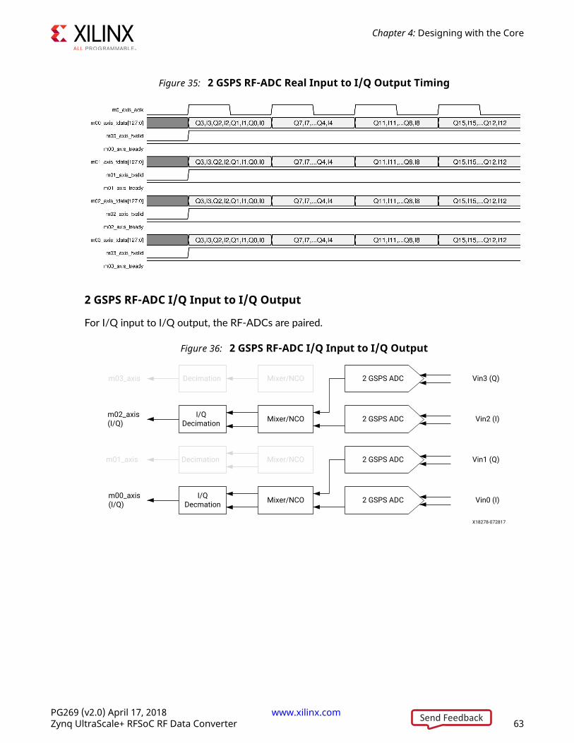
Figure 35: 2 GSPS RF-ADC Real Input to I/Q Output Timing
2 GSPS RF-ADC I/Q Input to I/Q Output
For I/Q input to I/Q output, the RF-ADCs are paired.
Figure 36: 2 GSPS RF-ADC I/Q Input to I/Q Output
2 GSPS ADCDecimation
I/QDecimation
Decimation
I/QDecmation
Mixer/NCOm03_axis
m02_axis (I/Q)
m01_axis
m00_axis (I/Q)
Vin3 (Q)
2 GSPS ADCMixer/NCO Vin2 (I)
2 GSPS ADCMixer/NCO Vin1 (Q)
2 GSPS ADCMixer/NCO Vin0 (I)
X18278-072817
Chapter 4: Designing with the Core
PG269 (v2.0) April 17, 2018 www.xilinx.com [placeholder text]Zynq UltraScale+ RFSoC RF Data Converter 63Send Feedback

Figure 37: 2 GSPS RF-ADC I/Q Input to I/Q Output IP Core Configuration
The following figure shows a 2 GSPS RF-ADC I/Q to I/Q, 1x decimation, the mixer enabled, andrunning at a 500 MHz AXI4-Stream clock.
Figure 38: 2 GSPS RF-ADC I/Q Input to I/Q Output Timing
Chapter 4: Designing with the Core
PG269 (v2.0) April 17, 2018 www.xilinx.com [placeholder text]Zynq UltraScale+ RFSoC RF Data Converter 64Send Feedback
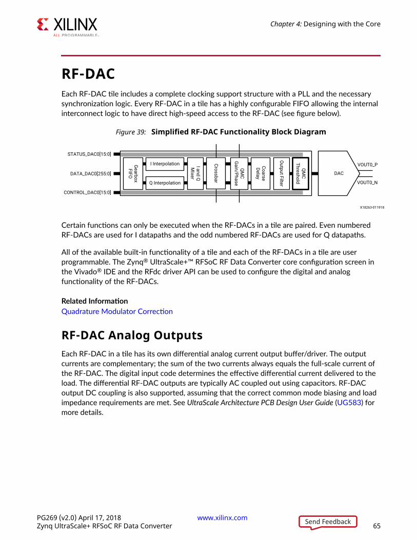
RF-DACEach RF-DAC tile includes a complete clocking support structure with a PLL and the necessarysynchronization logic. Every RF-DAC in a tile has a highly configurable FIFO allowing the internalinterconnect logic to have direct high-speed access to the RF-DAC (see figure below).
Figure 39: Simplified RF-DAC Functionality Block Diagram
QM
CThreshold
Coarse Delay
I and Q
Mixer
I Interpolation
Q Interpolation
GearboxFIFO
Output Filter
VOUT0_P
VOUT0_N
STATUS_DAC0[15:0]
CONTROL_DAC0[15:0]
DATA_DAC0[255:0] DAC
Crossbar
QM
CG
ain/Phase
X18263-011918
Certain functions can only be executed when the RF-DACs in a tile are paired. Even numberedRF-DACs are used for I datapaths and the odd numbered RF-DACs are used for Q datapaths.
All of the available built-in functionality of a tile and each of the RF-DACs in a tile are userprogrammable. The Zynq® UltraScale+™ RFSoC RF Data Converter core configuration screen inthe Vivado® IDE and the RFdc driver API can be used to configure the digital and analogfunctionality of the RF-DACs.
Related InformationQuadrature Modulator Correction
RF-DAC Analog OutputsEach RF-DAC in a tile has its own differential analog current output buffer/driver. The outputcurrents are complementary; the sum of the two currents always equals the full-scale current ofthe RF-DAC. The digital input code determines the effective differential current delivered to theload. The differential RF-DAC outputs are typically AC coupled out using capacitors. RF-DACoutput DC coupling is also supported, assuming that the correct common mode biasing and loadimpedance requirements are met. See UltraScale Architecture PCB Design User Guide (UG583) formore details.
Chapter 4: Designing with the Core
PG269 (v2.0) April 17, 2018 www.xilinx.com [placeholder text]Zynq UltraScale+ RFSoC RF Data Converter 65Send Feedback

Transmit Transfer Function
The differential output provides the maximum output current when all digital input bits are High.The output current (using binary format) is shown in the following equations.
Where:
1. BInDataIn = 14-bit digital input
2. IOUTFS = Full-scale output current
The output current (using a twos complement) is shown in the following equations.
Where:
1. TwosDataIN = 14-bit digital twos complement input ranging from (–2N-1) to (2N-1–1)
2. IOUTFS = Full-scale output current.
RF-DAC Output Current Mode
The RF-DAC output current is configurable, with an option of operating in either 20 mA or32 mA modes. In the 20 mA mode, set the DAC_AVTT to 2.5V and in the 32 mA mode, set it to3.0V to maintain the linearity performance.
CAUTION!: A 3.0V DAC_AVTT should not be used in the 20 mA mode. This risks exceeding themaximum ratings of the device and also risks affecting device reliability.
The output current can be set in the Advanced tab in the IP core configuration screen (see thefollowing figure) or using the RFdc driver API.
Chapter 4: Designing with the Core
PG269 (v2.0) April 17, 2018 www.xilinx.com [placeholder text]Zynq UltraScale+ RFSoC RF Data Converter 66Send Feedback
Figure 40: RF-DAC Output Current Configuration
RFdc Driver API Commands
// Set output current of RF-DAC Tile1, Block2 to 32mAXRFdc_GetOutputCurr(ptr, 1, 2, XRFDC_OUTPUT_CURRENT_32MA);
Related InformationXRFdc_GetOutputCurr
RF-DAC Nyquist Zone OperationEach RF-DAC can optimize its output response in the second Nyquist zone by using the mix-mode feature. This feature mixes the RF-DAC data with the sample clock, and, as a result,increases the output power in the second Nyquist zone, while attenuating it in the first Nyquistzone. This is shown in the following figure.
Chapter 4: Designing with the Core
PG269 (v2.0) April 17, 2018 www.xilinx.com [placeholder text]Zynq UltraScale+ RFSoC RF Data Converter 67Send Feedback

Figure 41: RF-DAC Nyquist Zone Operation
For normal (non-mix mode) operation, the blue line represents the ideal RF-DAC output roll-offsinc response. As can be seen, an output image in the second Nyquist zone in this mode wouldbe severely attenuated. An inverse sinc filter is available to compensate for the roll-off in the firstNyquist zone for this mode. See RF-DAC Inverse Sinc Filter for more information.
In RF-DAC mix-mode, the red line represents the ideal RF-DAC output response. In this mode,the output power of the image in the second Nyquist zone is significantly increased, and it alsohas an approximately flat response across the majority of the zone. The Nyquist zone can be setin the Vivado® IDE.
Related InformationRF-DAC Inverse Sinc Filter
RF-DAC Inverse Sinc FilterThe analog output response of the RF-DAC follows a characteristic sinx/x, or sinc shape. Forapplications that require flat-output response over a wide bandwidth, an inverse sinc filter isavailable to achieve this. The inverse sinc filter is an 11-tap FIR, which provides a flat-responsewith less than ±0.05 dB of ripple up to 89% of Nyquist, or ± 0.033 dB of ripple up to 80% ofNyquist. The following figure shows the inverse sinc performance.
Chapter 4: Designing with the Core
PG269 (v2.0) April 17, 2018 www.xilinx.com [placeholder text]Zynq UltraScale+ RFSoC RF Data Converter 68Send Feedback

Figure 42: Inverse Sinc Frequency Response
The line in blue represents the frequency response of the filter itself. As can be seen, it increaseswith frequency to compensate for the sinc response of the output, as shown by the red line. Thecomposite output response is given by the yellow trace, and shows a flat pass-band up to 89% ofNyquist. The following figure shows the detail of the corrected response, with ripple specificationlevels highlighted in red.
Chapter 4: Designing with the Core
PG269 (v2.0) April 17, 2018 www.xilinx.com [placeholder text]Zynq UltraScale+ RFSoC RF Data Converter 69Send Feedback
Figure 43: Inverse Sinc Detail
Inverse Sinc Filter Use
The filter can be enabled or disabled per RF-DAC in the Vivado® IDE by using the Inverse SincFilter checkbox, as shown in the following figure.
Figure 44: Inverse Sinc Configuration
RFdc Driver API Commands
The RFdc driver API can be used to get the inverse sinc enable state using the following code.
// Get Inverse Sinc State for Tile0, DAC Block1
int Tile = 0;u32 Block = 1;u32 isinc_enabled;isinc_enabled = XRFdc_GetInverseSincFilter (ptr, Tile, Block);xil_printf("DAC%d,%d Inverse Sinc Enabled: %d\n\r", Tile, Block, isinc_enabled);
Chapter 4: Designing with the Core
PG269 (v2.0) April 17, 2018 www.xilinx.com [placeholder text]Zynq UltraScale+ RFSoC RF Data Converter 70Send Feedback

Related InformationXRFdc_GetInverseSincFilter
Overflow
As seen in the Inverse Sinc Frequency response, the filter gain is >1, and increases withfrequency up to approximately 2.4 dB at 80% of Nyquist. To ensure that the filter output doesnot overflow, the input signal amplitude must be backed-off to account for this gain factor. Theinverse sinc block has automatic overflow detection and saturation, and if overflow is detected, itis flagged using the interrupt mechanism to the RFdc driver API, using theXRFDC_DAC_IXR_INVSNC_OF_MASK interrupt. For more details see Interrupt Handling.
Related InformationInterrupt Handling
Inverse Sinc Filter Details
Inverse Sinc FIR -1 3 -6 15 -52 594 -52 15 -6 3 -1
RF-DAC Digital DatapathEach RF-DAC in a tile has a number of optimized DSP features that can be used to implementDigital Up Conversion (DUC) and transmit signal filtering. These features are:
• Signal interpolation function - interpolation by x1 (bypass), ×2, ×4, or ×8 is supported
• Coarse mixing (quarter and half rate) or fine mixing with a 48-bit frequency resolutionnumerically controlled oscillator (NCO)
• Compensation functionality containing a quadrature modulator correction (QMC) block withcoarse delay adjustment block
• Signal conditioning containing an inverse sinc FIR filter
Single, multiple, or all DSP functions can be used or bypassed, using the Vivado® IDE.
The following figure shows the available functions in a RF-DAC. Each function is described in thefollowing sections.
Chapter 4: Designing with the Core
PG269 (v2.0) April 17, 2018 www.xilinx.com [placeholder text]Zynq UltraScale+ RFSoC RF Data Converter 71Send Feedback
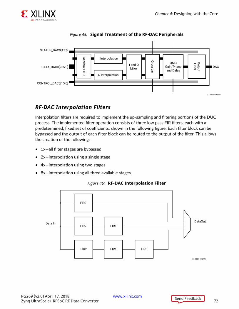
Figure 45: Signal Treatment of the RF-DAC Peripherals
DATA_DAC0[255:0]
STATUS_DAC0[15:0]
CONTROL_DAC0[15:0]
Gearbox FIFO
I Interpolation
Q Interpolation
I and Q Mixer
Crossbar
QMCGain/Phaseand Delay
Output
Filter DAC
X18266-091117
RF-DAC Interpolation Filters
Interpolation filters are required to implement the up-sampling and filtering portions of the DUCprocess. The implemented filter operation consists of three low pass FIR filters, each with apredetermined, fixed set of coefficients, shown in the following figure. Each filter block can bebypassed and the output of each filter block can be routed to the output of the filter. This allowsthe creation of the following:
• 1x—all filter stages are bypassed
• 2x—interpolation using a single stage
• 4x—interpolation using two stages
• 8x—interpolation using all three available stages
Figure 46: RF-DAC Interpolation Filter
Data InFIR2 FIR1
DataOut
FIR2 FIR1 FIR0
FIR2
X18267-112717
Chapter 4: Designing with the Core
PG269 (v2.0) April 17, 2018 www.xilinx.com [placeholder text]Zynq UltraScale+ RFSoC RF Data Converter 72Send Feedback

The output of an interpolated signal is the exact representation of the original signal presented ata higher sampling rate. Up-sampling of a signal sampled at F1 to a higher sample rate (N*F1)results in N replications of the original spectrum. Low pass filtering of the result helps to removeunwanted replications resulting in the preservation of the original signal at the required highersample rate.
Table 41: Interpolation Filter Operating Modes
Mode DescriptionOFF Filter is disabled, RF-DAC is not available.
1x Filter is bypassed.
2x 2x interpolation, 80% Nyquist passband.
4x 4x interpolation, 80% Nyquist passband.
8x 8x interpolation, 80% Nyquist passband.
Each of the filter stages can overflow—given the step-response of a FIR filter, especially whenfull-scale data is on the input. Each filter stage has an overflow status signal and outputsaturation to detect an overflow and protect the datapath. When a filter stage is not used, theoverflow flag is pulled Low. These flags are connected to the datapath interrupts mechanism.
Related InformationInterrupt Handling
Interpolation Filter Use
The IP core is used to set the interpolation rate. This is an IP core setting because changing theinterpolation rate directly affects the physical interface as the bandwidth to the PL changes. Thefilters that are enabled are shown in the following figure.
Chapter 4: Designing with the Core
PG269 (v2.0) April 17, 2018 www.xilinx.com [placeholder text]Zynq UltraScale+ RFSoC RF Data Converter 73Send Feedback
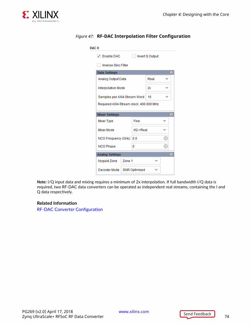
Figure 47: RF-DAC Interpolation Filter Configuration
Note: I/Q input data and mixing requires a minimum of 2x interpolation. If full bandwidth I/Q data isrequired, two RF-DAC data converters can be operated as independent real streams, containing the I andQ data respectively.
Related InformationRF-DAC Converter Configuration
Chapter 4: Designing with the Core
PG269 (v2.0) April 17, 2018 www.xilinx.com [placeholder text]Zynq UltraScale+ RFSoC RF Data Converter 74Send Feedback
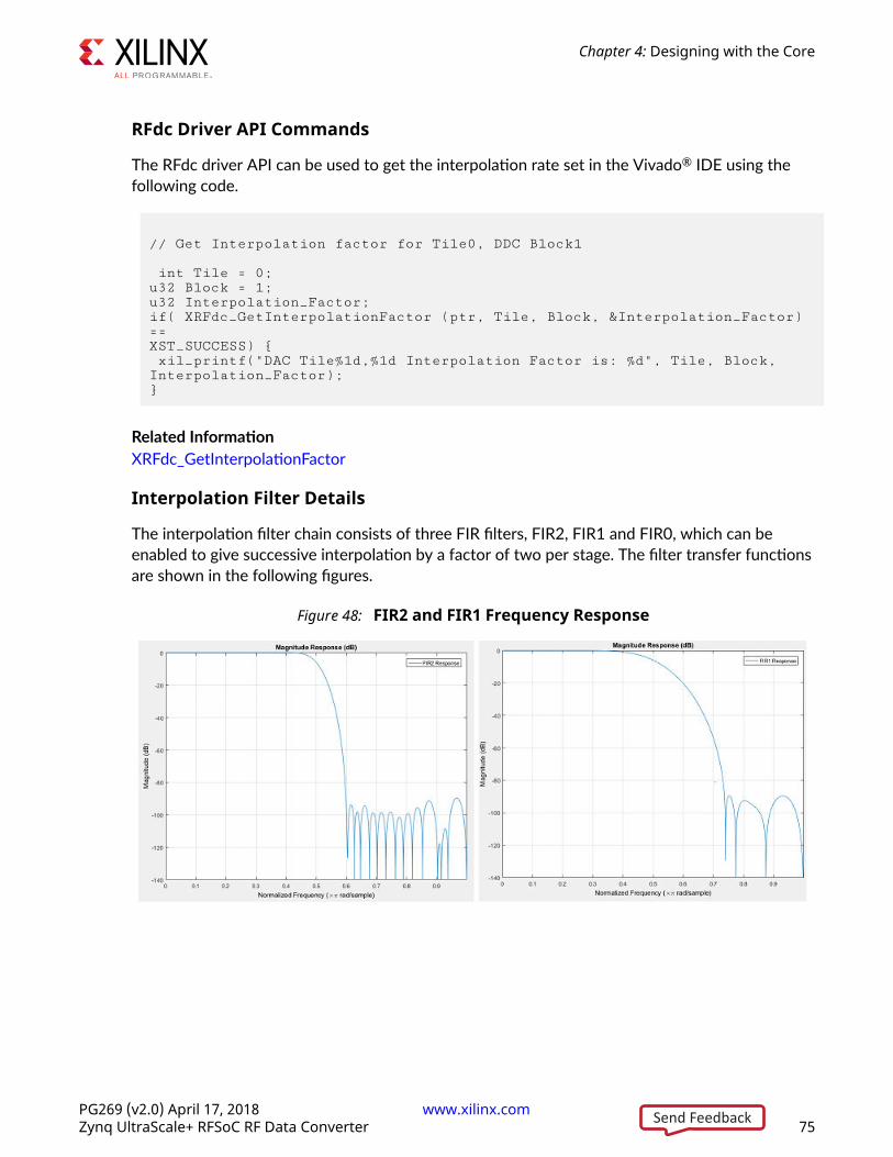
RFdc Driver API Commands
The RFdc driver API can be used to get the interpolation rate set in the Vivado® IDE using thefollowing code.
// Get Interpolation factor for Tile0, DDC Block1
int Tile = 0;u32 Block = 1;u32 Interpolation_Factor;if( XRFdc_GetInterpolationFactor (ptr, Tile, Block, &Interpolation_Factor) == XST_SUCCESS) xil_printf("DAC Tile%1d,%1d Interpolation Factor is: %d", Tile, Block, Interpolation_Factor);
Related InformationXRFdc_GetInterpolationFactor
Interpolation Filter Details
The interpolation filter chain consists of three FIR filters, FIR2, FIR1 and FIR0, which can beenabled to give successive interpolation by a factor of two per stage. The filter transfer functionsare shown in the following figures.
Figure 48: FIR2 and FIR1 Frequency Response
Chapter 4: Designing with the Core
PG269 (v2.0) April 17, 2018 www.xilinx.com [placeholder text]Zynq UltraScale+ RFSoC RF Data Converter 75Send Feedback

Figure 49: FIR0 and 2x Interpolation Frequency Response
Figure 50: 4x Interpolation and 8x Interpolation Frequency Response
The filter coefficients for the interpolation filters are shown in the following tables.
FIR2
1st Half5 0 -17 0 44 0 -96 0 187 0 -335 0 565 0 -906
0 1401 0 -2112 0 3145 0 -4723 0 7415 0 -13331 0 41526
CentreTap 65536
2ndHalf
5 0 -17 0 44 0 -96 0 187 0 -335 0 565 0 -906
0 1401 0 -2112 0 3145 0 -4723 0 7415 0 -13331 0 41526
FIR1
1st Half -12 0 84 0 -337 0 1008 0 -2693 0 10142
Centre Tap 16384
2nd Half -12 0 84 0 -337 0 1008 0 -2693 0 10142
Chapter 4: Designing with the Core
PG269 (v2.0) April 17, 2018 www.xilinx.com [placeholder text]Zynq UltraScale+ RFSoC RF Data Converter 76Send Feedback

FIR0
1st Half -6 0 54 0 -254 0 1230
Centre Tap 2048
2nd Half -6 0 54 0 -254 0 1230
The interpolation filter chains can operate in real or I/Q modes, depending on the data typeselected for the RF-DAC interface.
Related InformationRF-DAC Programmable Logic Data Interface
RF-DAC Numerical Controlled Oscillator and Mixer
The mixer function has three modes, bypass (no mixing), coarse mixing or fine mixing. Fine mixingautomatically enables the NCO which is used to generate the carrier frequency. The mixersupports full quadrature mixing, with both real to I/Q and I/Q to I/Q modes supported.
Figure 51: RF-DAC Mixer with NCO DSP Block
NCO
Fine Mixer
Coarse MixerN0, Fs/4, Fs/2, or -Fs/4
QIN
IINIOUT
QOUT
3 dB
3 dB
X18261-032318
Chapter 4: Designing with the Core
PG269 (v2.0) April 17, 2018 www.xilinx.com [placeholder text]Zynq UltraScale+ RFSoC RF Data Converter 77Send Feedback

Coarse Mixer:
• The coarse mixer allows the data to be mixed with a carrier of 0, Fs/2, Fs/4, or –Fs/4.
• Mixing with a 0 carrier bypasses the mixer component.
Fine Mixer:
• The fine mixer allows the data to be shifted up or down in frequency by an arbitrary amount.
• The frequency shift amount is obtained by programming the mixer frequency generated in theNCO. The fine mixer also supports 18-bit phase adjustment.
• The NCO phase can be synchronized within a tile using XRFdc_UpdateEvent.
• The NCO phase can be synchronized across tiles using an external event signal (SYSREF orMARKER).
• To manage potential overflow, the fine mixer output includes 3 dBV attenuation, as shown inthe figure above. This attenuation is set to -3 dBV (multiplication factor = 0.707) regardless ofthe RF-DAC setting in the RFdc driver API. A manual selection is also possible, allowing 0 dBVor -3 dBV.
The mixer settings can be configured in the core, or by using the RFdc driver API. The core isused to set the initial mixer settings (for example, mixer type and mixer mode), and the RFdcdriver API is used to adjust the settings at runtime. Both the RFdc driver API and the corecompute the required register settings based on the supplied sample rates and desiredfrequencies.See the RF-DAC Converter Configuration section for information on the settings.
Related InformationRF-DAC Converter Configuration
RF-DAC Multi-band OperationMulti-band operation is where two or more baseband signals are up-converted (mixed) toindividual carriers and then combined to generate a single composite analog output. In the RF-DAC tiles, this involves combining multiple DUC blocks together to drive the analog outputs.
The RF-DAC multi-band feature supports the following configurations:
• 2x multi-band real data per pair. One RF-DAC output of the pair is enabled; the other is off.
• 2x multi-band I/Q data per pair. Both RF-DACs in the pair are enabled, one for I and one forQ.
• 4x multi-band real data per tile. Four input streams are combined to drive the DAC0 output inreal mode. All other RF-DACs are off.
• 4x multi-band I/Q data per tile. Four input streams are combined to drive the DAC0 output asI and DAC1 output as Q. All other RF-DACs are off.
Chapter 4: Designing with the Core
PG269 (v2.0) April 17, 2018 www.xilinx.com [placeholder text]Zynq UltraScale+ RFSoC RF Data Converter 78Send Feedback

Latency between outputs in a multi-band pair is matched and latency between pairs is matched,irrespective of the mode.
When multi-band is off, the I and Q datapaths pass straight through the multi-band logic block(as shown below). When multi-band is on, I and Q of each datapath are combined and passed tothe next DSP block in the chain in front of the RF-DAC. Multi-band can be turned on per RF-DAC, for only the I datapath or the Q datapath, or for both I and Q.
Figure 52: Multi-band Logic
I Datapath
Q Datapath
IIN
IOUT
QOUT
QIN
IIN
QIN
X18269-081017
RF-DAC multi-band is implemented by connecting multiple RF-DAC DUC blocks to an RF-DACanalog block. Each DUC block handles one band of data, and can mix this up to any carrierfrequency. The output is then summed before being sent to the analog datapath and RF-DACoutput. This is shown in the following figure.
Chapter 4: Designing with the Core
PG269 (v2.0) April 17, 2018 www.xilinx.com [placeholder text]Zynq UltraScale+ RFSoC RF Data Converter 79Send Feedback

Figure 53: RF-DAC Digital Datapaths
DAC_X0Y0
Data Path 2 DAC2
Data Path 3 DAC3
Data Path 1 DAC1
Data Path 0 DAC0
s03_axis
s02_axis
s01_axis
s00_axis
RF-DAC Tile 2xReal MB, 2x Real
Q
I
Q
I
Q
I
Q
I
Vout3: 1 band
Vout2: 1 band
Vout1: Off
Vout0: 2x bands
DAC_X0Y0
Data Path 2 DAC2
Data Path 3 DAC3
Data Path 1 DAC1
Data Path 0 DAC0
s03_axis
s02_axis
s01_axis
s00_axis
RF-DAC Tile 2x I/Q MB
Q
I
Q
I
Q
I
Q
I
Vout3: Off
Vout2: Off
Vout1: 2x bands
Vout0: 2x bands -I
X19542-011918
Two example multi-band configurations are shown. The RF-DAC tile consists of four DUC blocks(digital datapaths) and four RF-DAC-analog blocks (analog datapaths). In the left hand example,the lower RF-DAC pair in the tile is configured as 2x real multi-band, while the top pair areindependent RF-DACs. Because the bottom pair uses two DUC blocks, DAC1 is off, and DAC0outputs the dual-band signal. In the right hand example, the lower pair is configured as 2x I/Qmulti-band, while the top pair is off.
RF-DAC Programmable Logic Data InterfaceThe data interface between the RF-DAC tiles and the PL is implemented using parallel datastreams, using the AXI4-Stream protocol. These data streams are input to gearbox FIFOs thatprovide a flexible interface between the user application and the RF-DAC tile. The maximuminterface width is 256 bits per stream, representing up to 16 16-bit big endian words. The datastreams and associated FIFOs have a configurable number of words which provide the flexibilityto choose between the number of words and the clock frequency to interface with the PL design.There are four streams per tile, and the naming convention is sXY_axis, where X represents theRF-DAC tile number, and Y represents a stream input to the FIFO in that tile. The following figureshows the interfaces.
Chapter 4: Designing with the Core
PG269 (v2.0) April 17, 2018 www.xilinx.com [placeholder text]Zynq UltraScale+ RFSoC RF Data Converter 80Send Feedback

Figure 54: RF-DAC Data Interfaces
6.5 GSPS DACInterpolation Mixer/NCO(Bypass)
s03_axis256-bit
s02_axis256-bit
s01_axis256-bit
s00_axis256-bit
Vout3
6.5 GSPS DACMixer/NCO(Bypass) Vout2
6.5 GSPS DACMixer/NCO(Bypass) Vout1
6.5 GSPS DACMixer/NCO(Bypass) Vout0
Interpolation
Interpolation
Interpolation
X19539-032718
Interface Data Formats
The data streams represent real or I/Q data, depending on the RF-DAC tile configuration. For RF-DAC tiles, a given stream is either real or I/Q interleaved. If an RF-DAC is configured with I/Qinput data then the even numbered samples of the stream represent I data and the odd-numbered samples represent Q data. These real and I/Q configurations are shown in RF-DAC IPConfiguration.
In each configuration all the enabled RF-DAC FIFOs in a tile begin to accept data when thepower-up sequence has completed. This is indicated by the assertion of the sXY_axis_treadyoutputs. If the data for any stream is not valid at this point, logic to suppress it should be includedin the PL.
Related InformationRF-DAC IP Configuration
Interface Data and Clock Rates
The total data rate per channel to the PL is determined by a number of factors, RF-DAC samplerate, interpolation factor, and I/Q and Real data formats. The gearbox FIFOs provide a way ofinterfacing this data rate to the clock frequency of the PL design, by allowing the number ofwords per clock to be chosen. The only requirements are that the interface number of words andclock rate combine to match the data rate required by the RF-DAC channel, and all RF-DACs in atile share a common interface clock frequency. This is shown by the following equations:
Chapter 4: Designing with the Core
PG269 (v2.0) April 17, 2018 www.xilinx.com [placeholder text]Zynq UltraScale+ RFSoC RF Data Converter 81Send Feedback

The IP core automatically calculates the data rates based on the RF-DAC sample rate anddatapath settings. This is shown in the following figure.
Figure 55: RF-DAC Data Interface Data and Clock Configuration
Each tile has independent clocking; sample rates, clock rates, PL rates, and configurations can bespecified on a per-tile basis.
Related InformationRF-DAC Converter Configuration
PL Clock Interface
The AXI4-Stream data for all four tile streams is synchronous to a clock from the PL, which has anaming convention of sX_axis_aclk, where X represents the RF-DAC tile number. This clockmust be at the frequency specified by the Required AXI4-Stream clock displayed on the IP coreconfiguration screen.
The RF-DAC tile also outputs a clock that can be used by the PL. This output clock is a dividedversion of the RF-DAC sample clock and therefore is frequency locked to it. This clock has anaming convention of clk_dacX, where X represents the RF-DAC tile number.
Related InformationClocking
Chapter 4: Designing with the Core
PG269 (v2.0) April 17, 2018 www.xilinx.com [placeholder text]Zynq UltraScale+ RFSoC RF Data Converter 82Send Feedback
Interface FIFO Overflow
The data rate through the interface gearbox FIFOs must be constant during runtime of the RF-DAC tile, with no frequency drift between the PL clock and RF-DAC analog sample clockdomains. If there is a frequency mismatch between these domains, a FIFO overflow can occur.The interface FIFOs have a built-in feature to determine if FIFO overflow has occurred, which isflagged to the PL through the IP interrupt mechanism.
There are two types of overflow: actual and marginal. Actual overflow indicates that the FIFOread/write pointers are overlapping, which means data is not being transferred safely betweendomains, and action must be taken. Marginal overflow is a warning and indicates that the FIFOread/write pointers are close to overlapping. Overflow should not occur during normal operation,and if overflow is seen it is an indication that the clocking infrastructure of the PL/PCB/IP core isincorrectly configured.
Related InformationInterrupt Handling
Synchronization
The gearbox FIFOs provide a flexible data and clock interface for the RF-DAC tiles. However, aswith all dual-clock FIFOs, latency might vary between one tile and another. While all channelswithin a tile have the same latency, some applications might require more than one RF-DAC tileto be used, and require the latencies to be matched across all RF-DAC channels. Theseapplications can use the Multi-Converter Synchronization feature to achieve this inter-tilesynchronization.
Related InformationMulti-Converter Synchronization
RF-DAC IP ConfigurationThe RF-DAC can be configured in several modes. The basic configuration options are available onthe IP core configuration screen in the Vivado® IDE and advanced operating modes can beconfigured using the RFdc driver API.
Chapter 4: Designing with the Core
PG269 (v2.0) April 17, 2018 www.xilinx.com [placeholder text]Zynq UltraScale+ RFSoC RF Data Converter 83Send Feedback

RF-DAC Real Input to Real Output
Figure 56: RF-DAC Real Input to Real Output
6.5 GSPS DACInterpolation Mixer/NCO(Bypass)s03_axis (Real)
s02_axis (Real)
s01_axis (Real)
s00_axis (Real)
Vout3 (Real)
6.5 GSPS DACMixer/NCO(Bypass)
Vout2 (Real)
6.5 GSPS DACMixer/NCO(Bypass)
Vout1 (Real)
6.5 GSPS DACMixer/NCO(Bypass)
Vout0 (Real)
Interpolation
Interpolation
Interpolation
X18284-032718
Chapter 4: Designing with the Core
PG269 (v2.0) April 17, 2018 www.xilinx.com [placeholder text]Zynq UltraScale+ RFSoC RF Data Converter 84Send Feedback
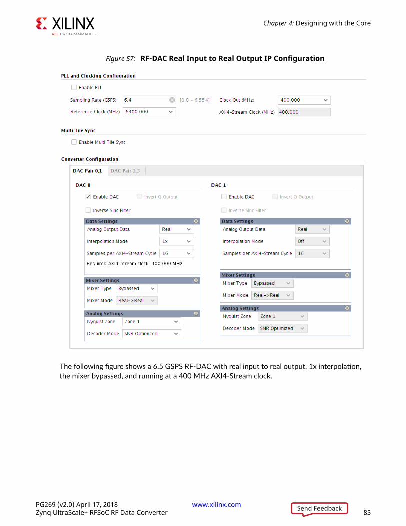
Figure 57: RF-DAC Real Input to Real Output IP Configuration
The following figure shows a 6.5 GSPS RF-DAC with real input to real output, 1x interpolation,the mixer bypassed, and running at a 400 MHz AXI4-Stream clock.
Chapter 4: Designing with the Core
PG269 (v2.0) April 17, 2018 www.xilinx.com [placeholder text]Zynq UltraScale+ RFSoC RF Data Converter 85Send Feedback

Figure 58: RF-DAC Real Input to Real Output Data Timing
RF-DAC I/Q Input to Real Output
Figure 59: RF-DAC I/Q Input to Real Output
6.5 GSPS DACI/QInterpolation Mixer/NCOs03_axis (I & Q)
s02_axis (I & Q)
s01_axis (I & Q)
s00_axis (I & Q)
Vout3 (Real)
6.5 GSPS DACMixer/NCO Vout2 (Real)
6.5 GSPS DACMixer/NCO Vout1 (Real)
6.5 GSPS DACMixer/NCO Vout0 (Real)
I/QInterpolation
I/QInterpolation
I/QInterpolation
X18279-032718
Chapter 4: Designing with the Core
PG269 (v2.0) April 17, 2018 www.xilinx.com [placeholder text]Zynq UltraScale+ RFSoC RF Data Converter 86Send Feedback

Figure 60: RF-DAC I/Q Input to Real Output IP Core Configuration
The following figure shows a 6.5 GSPS RF-DAC with I/Q input to real output, 2x interpolation,the mixer bypassed, and running at a 400 MHz AXI4-Stream clock.
Chapter 4: Designing with the Core
PG269 (v2.0) April 17, 2018 www.xilinx.com [placeholder text]Zynq UltraScale+ RFSoC RF Data Converter 87Send Feedback

Figure 61: RF-DAC I/Q Input to Real Output Timing
Note: Interpolation is x2 because the bandwidth available on the AXI4-Stream interface is limited.
RF-DAC I/Q Input to I/Q Output
For I/Q input to I/Q output, the RF-DACs are paired. An I/Q output signal requires a pair of RF-DACs, one for I data and one for Q data. As shown in the following figure, a single DUC blockoutputs I and Q data and these signals are sent to the two RF-DACs.
Figure 62: RF-DAC I/Q Input to I/Q Output
6.5 GSPS DACInterpolation
I/QInterpolation
Interpolation
I/QInterpolation
s03_axis
s02_axis (I & Q)
s01_axis
s00_axis (I & Q)
Vout3 (Q)
6.5 GSPS DAC Vout2 (I)
6.5 GSPS DACMixer/NCO Vout1 (Q)
6.5 GSPS DACMixer/NCO Vout0 (I)
Mixer/NCO
Mixer/NCO
X18280-032718
Chapter 4: Designing with the Core
PG269 (v2.0) April 17, 2018 www.xilinx.com [placeholder text]Zynq UltraScale+ RFSoC RF Data Converter 88Send Feedback

Figure 63: RF-DAC I/Q Input to I/Q Output IP Core Configuration
The following figure shows a 6.5 GSPS RF-DAC with I/Q input data to I/Q output data with 2xinterpolation, the mixer bypassed, and with a 400 MHz AXI4-Stream clock.
Chapter 4: Designing with the Core
PG269 (v2.0) April 17, 2018 www.xilinx.com [placeholder text]Zynq UltraScale+ RFSoC RF Data Converter 89Send Feedback

Figure 64: RF-DAC I/Q Input to I/Q Output Data Timing
Note: Interpolation is x2 because the bandwidth available on the AXI4-Stream interface is limited.
Chapter 4: Designing with the Core
PG269 (v2.0) April 17, 2018 www.xilinx.com [placeholder text]Zynq UltraScale+ RFSoC RF Data Converter 90Send Feedback

Quadrature Modulator CorrectionWhen using an external analog quadrature mixer device, a pair of converters (either RF-ADC orRF-DAC) must be used to handle the I and Q datapaths after conversion. Due to external eventsor circumstances, errors or imbalances can be introduced in the analog I and Q signal pathswhich, if not corrected, can lead to system performance degradation. The necessary correctionsto restore any system from degrading are accomplished using the quadrature modulatorcorrection (QMC) circuit.
As shown in the following figure, the QMC circuit is for correction only. Error and/or imbalancedetection must be done by application-specific code in the internal interconnect logic.
Figure 65: Converter QMC Circuitry
QMCI Datapath
IGAIN
Phase QMCI Datapath
IOFFSET
OVR
QMCQ Datapath
IOFFSET
QMCQ Datapath
QGAIN
Flag
OVRIIN
QIN OVR
Flag
IOUT
Flag
Flag
QOUTOVR
X18260-072817
The QMC circuit can compensate for the following:
• Gain correction is done by multiplying the signal by a gain factor. This factor has a range of 0to 2.0, and individual factors can be applied to the I and Q datapaths. The output resolution ofthe block is 16 bits.
Chapter 4: Designing with the Core
PG269 (v2.0) April 17, 2018 www.xilinx.com [placeholder text]Zynq UltraScale+ RFSoC RF Data Converter 91Send Feedback

• Phase correction is achieved by adding a scaled fraction of Q to the I value. The result of thisaddition can result in a gain error that must be corrected by the gain error correction block.Phase correction has a range of approximately ±26 degrees.
• Offset correction is done by adding a fixed LSB value to the sampled signal.
For full QMC functionality, a pair of converters need to be set up and used in I/Q mode. Whendisabling the phase correction factor, the QMC block can supply gain and offset correction to aconverter used in real mode. In this case, the converters do not need to be paired to make use ofthe QMC block functions.
Update QMC SettingsThe gain, phase, and offset correction factor values can be set using the RFdc driver API. Anexample of using the API is as follows.
// Initial Setup
XRFdc_QMC_Settings QMC_Settings_I, QMC_Settings_Q; // RF-ADC block0 is I, RF-ADC block1 is QQMC_Settings_I.EventSource = XRFDC_EVNT_SRC_TILE; // QMC Settings are updated with a tile eventQMC_Settings_Q.EventSource = XRFDC_EVNT_SRC_TILE;
....// Update Gain/Phase/Offset for I/Q RF-DACs in tile0
QMC_Settings_I.GainCorrectionFactor = 0.9; // Set Gain for IQMC_Settings_I.PhaseCorrectionFactor = -5.0; // I/Q imbalance factor applied to I side, approx in degrees.QMC_Settings_I.EnableGain = 1;QMC_Settings_I.EnablePhase = 1;QMC_Settings_Q.GainCorrectionFactor = 0.95;QMC_Settings_Q.EnableGain = 1; XRFdc_SetQMCSettings(ptr, XRFDC_ADC_TILE, 0, 0, &QMC_Settings_I); // Write settings for ADC0,0 - I ADCXRFdc_SetQMCSettings(ptr, XRFDC_ADC_TILE, 0, 1, &QMC_Settings_Q); //Write settings for ADC0,1 - Q ADCXRFdc_UpdateEvent(ptr, XRFDC_ADC_TILE, 0, 0, XRFDC_EVENT_QMC); //Generate a Tile Update Event - applies all QMC Settings at once
It is also possible to read back the QMC settings from any converter, using theXRFdc_GetQMCSettings RFdc driver API command. This populates the QMC_Settingsstructure with the values from the hardware.
Chapter 4: Designing with the Core
PG269 (v2.0) April 17, 2018 www.xilinx.com [placeholder text]Zynq UltraScale+ RFSoC RF Data Converter 92Send Feedback

Related InformationXRFdc_SetQMCSettingsXRFdc_UpdateEvent
I/Q RF-ADC Naming ConventionWhen converters are used in an I/Q pair, the I channel always uses the even block numbers, andthe Q channel always uses the odd block numbers. For example, in a 4 GSPS RF-ADC tile, the IRF-ADC is block0, and the Q RF-ADC is block1. For 2 GSPS RF-ADC tiles, or RF-DAC tiles, the Ichannels are block0 and block2, while the related Q channels are block1 and block3, respectively.
QMC OverflowSetting excessive gain, phase or offset correction factors relative to the input signal can cause thedatapath to overflow. To aid system debug, the QMC block contains built-in overflow detectionand saturation blocks. These blocks generate flags which are connected to the IP interruptmechanism using the datapath interrupt. The related interrupt flags for the QMC block are:
XRFDC_IXR_QMC_GAIN_PHASE_MASK
XRFDC_IXR_QMC_OFFST_MASK
These interrupts can be enabled per converter channel.
• The gain correction multiplier range is between 0 and 2.0.
• The range of the phase correction multiplier is approximately ±26 degrees, or ±0.5 in terms ofmagnitude.
Related InformationInterrupt Handling
Chapter 4: Designing with the Core
PG269 (v2.0) April 17, 2018 www.xilinx.com [placeholder text]Zynq UltraScale+ RFSoC RF Data Converter 93Send Feedback
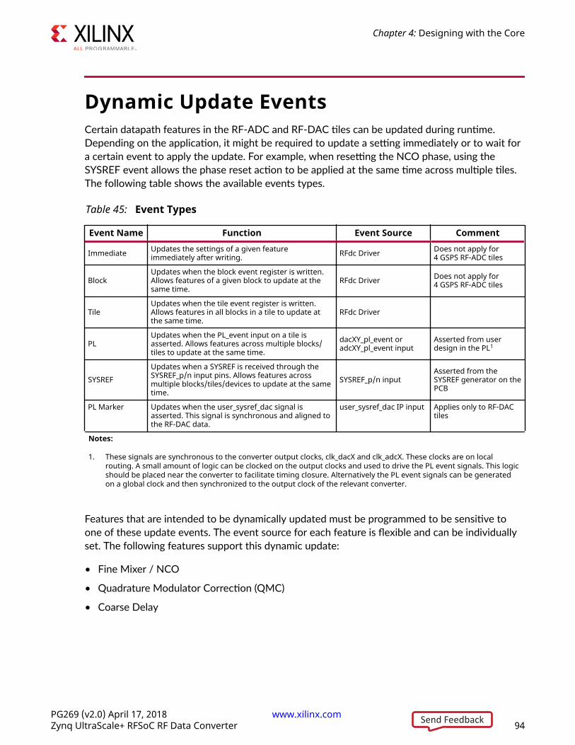
Dynamic Update EventsCertain datapath features in the RF-ADC and RF-DAC tiles can be updated during runtime.Depending on the application, it might be required to update a setting immediately or to wait fora certain event to apply the update. For example, when resetting the NCO phase, using theSYSREF event allows the phase reset action to be applied at the same time across multiple tiles.The following table shows the available events types.
Table 45: Event Types
Event Name Function Event Source Comment
Immediate Updates the settings of a given featureimmediately after writing. RFdc Driver Does not apply for
4 GSPS RF-ADC tiles
BlockUpdates when the block event register is written.Allows features of a given block to update at thesame time.
RFdc Driver Does not apply for4 GSPS RF-ADC tiles
TileUpdates when the tile event register is written.Allows features in all blocks in a tile to update atthe same time.
RFdc Driver
PLUpdates when the PL_event input on a tile isasserted. Allows features across multiple blocks/tiles to update at the same time.
dacXY_pl_event oradcXY_pl_event input
Asserted from userdesign in the PL1
SYSREFUpdates when a SYSREF is received through theSYSREF_p/n input pins. Allows features acrossmultiple blocks/tiles/devices to update at the sametime.
SYSREF_p/n inputAsserted from theSYSREF generator on thePCB
PL Marker Updates when the user_sysref_dac signal isasserted. This signal is synchronous and aligned tothe RF-DAC data.
user_sysref_dac IP input Applies only to RF-DACtiles
Notes:
1. These signals are synchronous to the converter output clocks, clk_dacX and clk_adcX. These clocks are on localrouting. A small amount of logic can be clocked on the output clocks and used to drive the PL event signals. This logicshould be placed near the converter to facilitate timing closure. Alternatively the PL event signals can be generatedon a global clock and then synchronized to the output clock of the relevant converter.
Features that are intended to be dynamically updated must be programmed to be sensitive toone of these update events. The event source for each feature is flexible and can be individuallyset. The following features support this dynamic update:
• Fine Mixer / NCO
• Quadrature Modulator Correction (QMC)
• Coarse Delay
Chapter 4: Designing with the Core
PG269 (v2.0) April 17, 2018 www.xilinx.com [placeholder text]Zynq UltraScale+ RFSoC RF Data Converter 94Send Feedback

Update Event UseThe RFdc driver API uses the EventSource parameter of a particular function to set up thetrigger event for that function. It can also issue a subset of the events. The following code showsan example of the setup of a tile event source followed by the tile event.
// Initial Setup - Mixer settings for 2 DDC blocks
XRFdc_Mixer_Settings Mixer_Settings_0;XRFdc_Mixer_Settings Mixer_Settings_1;
// Mixer Settings for both DDC blocks are updated with a tile event
Mixer_Settings_0.EventSource = XRFDC_EVNT_SRC_TILE;Mixer_Settings_1.EventSource = XRFDC_EVNT_SRC_TILE;....// Make changes to mixer settings and write them to both DDCs
Mixer_Settings_0.freq = 1.23;Mixer_Settings_1.freq = 1.43;XRFdc_SetMixerSettings (ptr, XRFDC_ADC_TILE, 0, 0, &Mixer_Settings_0);XRFdc_SetMixerSettings (ptr, XRFDC_ADC_TILE, 0, 1, &Mixer_Settings_1);
// Generate the event for DDC block 0// This maps to the Tile event, which updates both DDCs at the same moment
XRFdc_UpdateEvent(ptr, XRFDC_ADC_TILE, 0, 0, XRFDC_EVENT_MIXER);
Related InformationXRFdc_SetMixerSettingsXRFdc_UpdateEvent
PLLEach RF-ADC and RF-DAC tile includes a clocking system with an input clock divider, a PLL, andan output divider. When used with the SYSREF input, the clocking system can be synchronized inmulti-tile or multi-chip designs. When the PLL is used, the output sampling clock is fed to themultiplexer, which can also be used by a direct input clock before it is routed into the clocknetwork of the tile (as shown below). The clock from the PLL is used in both the analog anddigital portions of the RF-ADC or RF-DAC in a tile. Each RF-ADC or RF-DAC in a tile has a localdivider to divide and distribute the very low jitter clock from the PLL or a direct input to thedifferent functions in each RF-ADC or RF-DAC function.
Chapter 4: Designing with the Core
PG269 (v2.0) April 17, 2018 www.xilinx.com [placeholder text]Zynq UltraScale+ RFSoC RF Data Converter 95Send Feedback

Figure 66: Tile PLL Clocking Structure
PLL
SYSREFCapture
SYSREF distributionto adjacent tiles
Divider
Datapath logic
Datapath logic
CLK_adc/dac SYSREF
Sync Logic
X18215-041218De
mux
SYSREF
ClockDetector
adc/dac_clk_pCML
adc/dac_clk_n100 Ω
PLLDiv
Mux
SYSREF distributionto adjacent tiles
The operating parameters of the PLL are set using the Vivado® IDE to specify the default PLLconfiguration or by the RFdc driver API if runtime adjustment of the PLL is required. The PLLmust first be enabled in the Vivado IDE if runtime adjustment using the API is required.
The internal PLL block diagram is shown in the following figure. The API function dedicated toconfiguring the PLL system sets a reference divider (an integer from 1 to 4), feedback divider (aninteger from 13 to 160) and output divider (an integer from 2 to 64) to achieve the bestperformance of the PLL using the VCO in the correct range. In any frequency configuration, thebest performance of phase noise is achieved when the PLL system is able to select a referencedivider of 1.
Figure 67: PLL System
Reference Divider (R) PFD
CP
LPF
Feedback Divider
Output Divider (M)VCOInput
(Reference Frequency)
Output(PLL Frequency Output)
(VCO Frequency)
X20569-032918
Chapter 4: Designing with the Core
PG269 (v2.0) April 17, 2018 www.xilinx.com [placeholder text]Zynq UltraScale+ RFSoC RF Data Converter 96Send Feedback

Interrupt HandlingThe RF-ADCs and RF-DACs and tiles can generate interrupts during operation which can helpdebug or avoid potential issues. The interrupts are shown in the following table.
Table 46: Interrupts
Block Interrupt Description
RF-ADC Analog -OverVoltage
Indicates the analog input is exceeding the safe input range of the RF-ADC input bufferand the buffer has been shut down. The input signal amplitude and common modeshould be brought within range.
Related RFdc Driver API constraints:Enable All: XRFDC_ADC_IXR_OVRVOLT_MASK
RF-ADC/ RF-DAC Datapath QMC
Indicates the QMC gain/phase/offset correction has overflowed/saturated. Dataamplitude, or correction factors are too high and should be reduced.
Related RFdc Driver API constraints:Gain, Phase: XRFDC_IXR_QMC_GAIN_PHASE_MASK Offset:XRFDC_IXR_QMC_OFFST_MASK
RF-ADC DatapathDecimation
Indicates one of the decimation stages has overflowed/saturated. Flags are per-stageand I/Q paths to indicate where the overflow has occurred. Data amplitude is too high.
Related RFdc Driver API constraints:Enable All: XRFDC_ADC_IXR_DMON_STG_MASK I-Datapath, Stage 0, 1, 2:XRFDC_ADC_IXR_DMON_I_STG<0,1,2>_MASK Q-Datapath, Stage 0, 1, 2:XRFDC_ADC_IXR_DMON_Q_STG<0,1,2>_MASK
RF-DAC DatapathInterpolation
Indicates one of the interpolation stages has overflowed/saturated. Flags are per-stageand I / Q paths to indicate where the overflow has occurred. Data amplitude is toohigh.
Related RFdc Driver API constraints:Enable All: XRFDC_ADC_IXR_INTP_STG_MASK I-Datapath, Stage 0, 1, 2:XRFDC_DAC_IXR_INTP_I_STG<0, 1, 2>_MASK Q-Datapath, Stage 0, 1, 2:XRFDC_DAC_IXR_INTP_Q_STG<0, 1, 2>_MASK
RF-ADC Analog -OverRange
Indicates the analog input is exceeding the full-scale range of the RF-ADC. The inputsignal amplitude should be reduced.
Related RFdc Driver API constraints:Enable All: XRFDC_SUBADC_IXR_DCDR_MASK
RF-ADC/ RF-DAC FIFO Overflow
Indicates that the FIFO interface is incorrectly setup, clocks/data throughput mismatch.
Related RFdc Driver API constraints:Enable All: XRFDC_IXR_FIFOUSRDAT_MASK Actual Overflow:XRFDC_IXR_FIFOUSRDAT_OF_MASK || XRFDC_IXR_FIFOUSRDAT_UF_MASK MarginalOverflow: XRFDC_IXR_FIFOMRGNIND_OF_MASK ||XRFDC_IXR_FIFOMRGNIND_UF_MASK
RF-DAC DatapathInverse Sinc
Indicates the inverse sinc filter has overflowed/saturated. Data amplitude is too highand should be reduced.
Related RFdc Driver API constraints:Inverse Sinc: XRFDC_DAC_IXR_INVSNC_OF_MASK
The following figure shows the interrupt hierarchy within the IP core.
Chapter 4: Designing with the Core
PG269 (v2.0) April 17, 2018 www.xilinx.com [placeholder text]Zynq UltraScale+ RFSoC RF Data Converter 97Send Feedback

Figure 68: Interrupt Hierarchy
Programmable LogicZynq® UltraScale+™ RFSoC RF Data Converter
ADC Tile0InterruptStatus
Enable[3:0]
ADC Tile0, 0InterruptStatus
ADC Tile 0
DAC Tile 0
OverRangeOverVoltage
DataPathFIFO
Converter0
DataPathFIFO
Enable[1:0]
DAC Tile0, 0InterruptStatus
Converter0Converter2Converter1
Enable[3:0]
Converter0Converter2Converter1
Enable[3:0]
DAC Tile0InterruptStatus
Converter0
ADC3ADC2ADC1ADC0
DAC3DAC2DAC1DAC0
Common InterruptStatus
irqTo PS/MicroBlazeInterrupt Controller
Enable[7:0]
X19541-032918
Datapath overflow indicates that a sub-block in the signal chain has detected that the outputsignal amplitude has exceeded full scale, and has been saturated. If overflow is detected itindicates that either the signal amplitude is too high, or the block settings are incorrect for thesignal amplitude. For example, using a large gain correction factor on a signal that is close to full-scale causes a QMC gain overflow.
All of the interrupts shown in the previous figure are enabled and handled by the interruptfunctions of the RFdc driver API. The default interrupt status handler (XRFdc_IntrHandler)automatically follows the interrupt hierarchy in the previous figure to determine the source ofthe interrupt, and then passes this information to the user-defined status handler to respond.
Related InformationRF-DAC Interpolation FiltersQuadrature Modulator CorrectionRF-ADC Decimation FiltersClocking
Chapter 4: Designing with the Core
PG269 (v2.0) April 17, 2018 www.xilinx.com [placeholder text]Zynq UltraScale+ RFSoC RF Data Converter 98Send Feedback
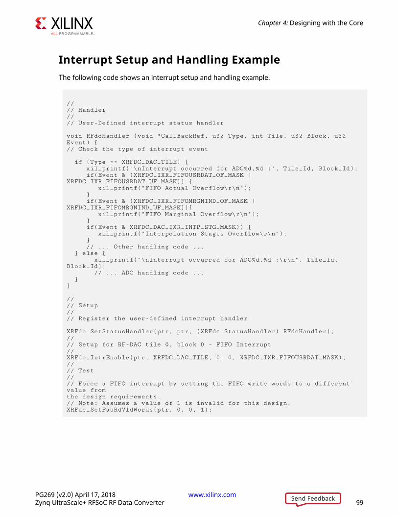
Interrupt Setup and Handling ExampleThe following code shows an interrupt setup and handling example.
//// Handler//// User-Defined interrupt status handler
void RFdcHandler (void *CallBackRef, u32 Type, int Tile, u32 Block, u32 Event) // Check the type of interrupt event
if (Type == XRFDC_DAC_TILE) xil_printf("\nInterrupt occurred for ADC%d,%d :", Tile_Id, Block_Id); if(Event & (XRFDC_IXR_FIFOUSRDAT_OF_MASK | XRFDC_IXR_FIFOUSRDAT_UF_MASK)) xil_printf("FIFO Actual Overflow\r\n"); if(Event & (XRFDC_IXR_FIFOMRGNIND_OF_MASK | XRFDC_IXR_FIFOMRGNIND_UF_MASK)) xil_printf("FIFO Marginal Overflow\r\n"); if(Event & XRFDC_DAC_IXR_INTP_STG_MASK)) xil_printf("Interpolation Stages Overflow\r\n"); // ... Other handling code ... else xil_printf("\nInterrupt occurred for ADC%d,%d :\r\n", Tile_Id, Block_Id); // ... ADC handling code ...
//// Setup//// Register the user-defined interrupt handler
XRFdc_SetStatusHandler(ptr, ptr, (XRFdc_StatusHandler) RFdcHandler);//// Setup for RF-DAC tile 0, block 0 - FIFO Interrupt//XRFdc_IntrEnable(ptr, XRFDC_DAC_TILE, 0, 0, XRFDC_IXR_FIFOUSRDAT_MASK);//// Test//// Force a FIFO interrupt by setting the FIFO write words to a different value from the design requirements. // Note: Assumes a value of 1 is invalid for this design.XRFdc_SetFabRdVldWords(ptr, 0, 0, 1);
Chapter 4: Designing with the Core
PG269 (v2.0) April 17, 2018 www.xilinx.com [placeholder text]Zynq UltraScale+ RFSoC RF Data Converter 99Send Feedback

This example shows the RFdc driver-specific interrupt handling and the forcing of an interrupt bychanging the FIFO parameters. The setup and registration of the RF Data Converter irq outputwith the PS or MicroBlaze™ interrupt controller is not shown. For more details, see the examplesprovided with the RFdc driver API (see the Zynq UltraScale+ Device Technical Reference Manual(UG1085)).
Related InformationXRFdc_IntrEnableXRFdc_SetFabRdVldWords
ClockingThe following table describes the clocks associated with the Zynq® UltraScale+™ RFSoC RF DataConverter IP core.
Table 47: IP Core Clocks
Clock Description
s_axi_aclkAXI4-Lite clock. This clock is common to all tiles in the core and should be driven by thesystem CPU used for the AXI4-Stream interconnect connected to the AXI4-Lite interface.This clock should be between 10 MHz and 200 MHz.
dac[3:0]_clk_p/nSampling Clock or Reference Clock to internal PLL for the RF-DAC tiles. There are up to fourdifferential clock inputs on the core because there is a maximum of four RF-DAC tilesavailable. This clock must be driven with the frequency chosen on the IP core configurationscreen.
adc[3:0]_clk_p/nSampling Clock or Reference Clock to internal PLL for the RF-ADC tiles. There are up to fourdifferential clock inputs on the core because there is a maximum of four RF-ADC tilesavailable. This clock must be driven with the frequency chosen on the IP core configurationscreen.
clk_dac[3:0]
Output clock to interconnect logic from the RF-DAC tiles. This is a user-configurable outputclock from the core to the user logic. The use of this clock is optional. It can be used to drivethe PL design if another frequency-locked RF-DAC sample clock is not available in the PL.The frequency of this clock output can be chosen from a list of values, related to the samplerate, in the IP core configuration screen.
clk_adc[3:0]
Output clock to interconnect logic from the RF-ADC tiles. This is a user-configurable outputclock from the core to the user logic. It can be used to drive the PL design if anotherfrequency-locked RF-ADC sample clock is not available in the PL. The frequency of this clockoutput can be chosen from a list of values, related to the sample rate, in the IP coreconfiguration screen.
s[3:0]_axis_aclk
Slave AXI4-Stream clocks for RF-DAC data interfaces. There are up to 16 AXI4-Streaminterfaces on the core, one per RF-DAC. Each RF-DAC tile has a single clock common to upto four AXI4-Stream data interfaces. All AXI4-Stream data interfaces on a tile must operateat the same clock rate but the bandwidth of each interface can be different because eachAXI4-Stream interface can have a different width as specified in the IP core configurationscreen. This clock must be frequency-locked to the RF-DAC sample clock as outlined inInterface FIFO Overflow.
Chapter 4: Designing with the Core
PG269 (v2.0) April 17, 2018 www.xilinx.com [placeholder text]Zynq UltraScale+ RFSoC RF Data Converter 100Send Feedback
Table 47: IP Core Clocks (cont'd)
Clock Description
m[3:0]_axis_aclk
Master AXI4-Stream clocks for RF-ADC data interfaces. There are up to eight or 16 AXI4-Stream interfaces on the core depending on the chosen device, one per RF-ADC. Each RF-ADC tile has a single clock common to up to two or four AXI4-Stream data interfaces. AllAXI4-Stream data interfaces on a tile must operate at the same clock rate; however thebandwidth of each interface can be different because each AXI4-Stream interface can havea different width as specified in the IP core configuration screen. This clock must befrequency-locked to the RF-ADC sample clock as outlined in Interface FIFO Overflow.
Related InformationInterface FIFO Overflow
Clock InputsEach RF-ADC or RF-DAC tile has its own clock input. There is no need to instantiate a clockinput buffer in your design because the current-mode logic (CML) clock input buffer isimplemented in the tile architecture. The clock input buffer can be used as a sampling clock forthe tile or as a reference for the tile PLL. The CML clock input has an on-die differentialtermination of 100 Ω.
The clock input buffer has a detection circuit for measuring activity at the external clock inputs.When a clock is present, the input buffer is activated. When no clock is present, the outputs ofthe clock buffer are forced into a steady state. If the clock is lost, the core shuts the tile down butwill restart the tile without user intervention when the clock returns.
When the PLL is not used, the clock buffer output is passed through a multiplexer into the RF-ADC or RF-DAC tile clock network. When the PLL is used, the output of the clock buffer isdriven to the PLL to serve as the reference clock.
In each Zynq® UltraScale+™ RFSoC, there is a dedicated input SYSREF pin pair per package. TheSYSREF clocks the multi-tile and multi-chip synchronization. For multi-tile designs, the SYSREFconnects into a master tile and the signal must be distributed from inside that tile to all othertiles used in the design.
The presence of a clock at the input pins can be checked by using the RFdc software API. If noclock is detected the RF-ADC and RF-DAC blocks affected do not start up and stay in the ClockDetection state.
Related InformationPower-up Sequence
Chapter 4: Designing with the Core
PG269 (v2.0) April 17, 2018 www.xilinx.com [placeholder text]Zynq UltraScale+ RFSoC RF Data Converter 101Send Feedback

Tile Clocking StructureThe following figures show the tile high-level clocking structure. The clocking structure in a tilestarts from a single clock source coming from the tile PLL or straight from the clock input pins.
For a tile to keep a low-jitter and high-speed clocking structure, a single input clock is routed toeach RF-ADC or RF-DAC in the tile and divided for the dedicated signal conditioning functionswithin the RF-ADC or RF-DAC.
Figure 69: RF-ADC Clock Structure in a Tile
Sync
Digital Functions Clock Domain
Internal Logic Clock Domain
RF-ADC RF-ADC RF-ADC RF-ADC
Clock
PLL
DIV
SYSREF
SyncAnalog Clock
Sync SyncCLK DriveCLKDrive
CLK DriveCLK Drive
Digital Clock Domain
Clk
Divider
clk_adcX Sync_Flag m_axis_aclk
X18249-080917
Chapter 4: Designing with the Core
PG269 (v2.0) April 17, 2018 www.xilinx.com [placeholder text]Zynq UltraScale+ RFSoC RF Data Converter 102Send Feedback

Figure 70: RF-DAC Clock Structure in a Tile
Internal Logic Clock Domain
Digital Functions Clock Domain
Digital Clock Domain
RF-DAC RF-DAC RF-DAC RF-DAC
Clock
PLL
DIV
SYSREF
Sync
Divider
clk_dacX Sync_Flag s_axis_aclk
SyncClk
Sync Sync
Analog Clock
X18216-080917
CLKDrive
CLKDrive
CLKDrive
CLKDrive
The clock coming out from the divider of the master tile can be used to drive the PL. A BUFG_GTbuffer is automatically instantiated by the IP core when the output clock is used.
The following figure shows the clock connections for a typical Zynq® UltraScale+™ RFSoC RFData Converter IP core. The IP core automatically instantiates and connects the constituent RF-ADC and RF-DAC tiles based on the selections in the Vivado® IDE.
Chapter 4: Designing with the Core
PG269 (v2.0) April 17, 2018 www.xilinx.com [placeholder text]Zynq UltraScale+ RFSoC RF Data Converter 103Send Feedback
Figure 71: IP Core Clocking
RF-ADC Tile
Zynq UltraScale+ RFSoC RF Data Converter IP
s_axi_aclk
adc0_clk_p
ADC_CLK_N CLK_ADCADC_CLK_P clk_adc0
DCLK
FABRIC_CLK
Sampling Clock or Reference Clock
BUFG
adc0_clk_n
s0_axis_aclk
RF-ADC Tile
ADC_CLK_N CLK_ADCADC_CLK_P
DCLK
FABRIC_CLK
clk_adc1adc1_clk_p
Sampling Clock or Reference Clock adc1_clk_n
s01_axis_aclk
AXI4-Stream Clock(Sample Clock)
AXI4-Lite Clock(CPU Clock)
BUFG
X18271-081117
In most applications the AXI4-Stream clock is common to multiple converters and is suppliedfrom an external clock as shown in the previous figure. This clock must be derived from the samemaster clock source as the sampling and/or reference clocks to the RF-ADC and RF-DAC tiles.Alternatively, it is possible to use the output of one of the RF-DAC or RF-ADC tiles to generatethe AXI4-Stream clocks as shown in the following figure.
Chapter 4: Designing with the Core
PG269 (v2.0) April 17, 2018 www.xilinx.com [placeholder text]Zynq UltraScale+ RFSoC RF Data Converter 104Send Feedback
Figure 72: Typical Clocking Scheme Using RF-ADC Output Clock as Data Clock
RF-ADC Tile
Zynq UltraScale+ RFSoC RF Data Converter
s_axi_aclk
adc0_clk_p
ADC_CLK_N CLK_ADCADC_CLK_P clk_adc0
DCLK
FABRIC_CLK
Sampling Clock or Reference Clock
BUFG_GT
adc0_clk_n
s0_axis_aclk
RF-ADC Tile
ADC_CLK_N CLK_ADCADC_CLK_P
DCLK
FABRIC_CLK
clk_adc1adc1_clk_p
Sampling Clock or Reference Clock adc1_clk_n
s01_axis_aclk
AXI4-Lite Clock(CPU Clock)
BUFG
MMCM(Optional)
BUFGTo User LogicAXI4-Stream
Interface
X18272-081117
ResetsStandard AXI4-Stream resets are provided for each clock domain. Reset of the RF-ADC and RF-DAC is done using the AXI4-Lite interface. A full tile reset is carried out by asserting bit 0 of theMaster Reset Register. Individual tiles can be reset and disabled by writing to the Restartregisters. Disabling the tile is achieved in a similar way. Follow the individual tile reset procedureto restart the tile after it has been disabled.
Related InformationMaster Reset Register (0x0004)Restart All TilesRestart TilePower-Down Tile
Chapter 4: Designing with the Core
PG269 (v2.0) April 17, 2018 www.xilinx.com [placeholder text]Zynq UltraScale+ RFSoC RF Data Converter 105Send Feedback

Power-up SequenceTiles consist of different independent blocks, powered from different power supplies and clockedby different versions of the main clock. Tiles must be brought up in a known sequence for theconverters to function correctly. The power-up state machine is run automatically when thedevice is configured or reconfigured with a bitstream but it can also be rerun at any time undersoftware control.
Figure 73: POR Finite State Machine
Device Power Up and Configuration
Power Supply Adjustment
Clock Configuration
Converter Calibration
Done
Supply Detectors
Clock Detector
X18500-081117
Power-on Sequence Steps
SequenceNumber State Description
0-2 Device Power-up andConfiguration
The configuration parameters set in the Vivado® IDE areprogrammed into the converters. The state machine then waits forthe external supplies to be powered up. In hardware this can take upto 25 ms. However this is reduced to 200 μs in behavioralsimulations.
3-5 Power Supply AdjustmentThe configuration settings are propagated to the analog sections ofthe converters. In addition the regulators, bias settings in the RF-DACand the common-mode output buffer in the RF-ADC are enabled.
6-10 Clock ConfigurationThe state machine first detects the presence of a good clock into theconverter. Then, if the PLL is enabled, it checks for PLL lock. Theclocks are then released to the digital section of the converters.
11-13 Converter Calibration (ADC only)Calibration is carried out in the RF-ADC. In hardware this can takeapproximately 10 ms, however this is reduced to 10 μs in behavioralsimulations.
15 Done The state machine has completed the power-up sequence.
Related InformationInterrupt HandlingRF-DAC/RF-ADC Tile <n> FIFO Disable Register (0x0230)
Chapter 4: Designing with the Core
PG269 (v2.0) April 17, 2018 www.xilinx.com [placeholder text]Zynq UltraScale+ RFSoC RF Data Converter 106Send Feedback

Restart All TilesTo restart all tiles and perform the complete power-on sequence after initialization undersoftware control, perform the following steps:
1. Write 0x0000_0001 to the Master Reset register to restart all tiles (start and end statesrevert to their default so there is no need to write 0x0000_000F to the individual tile RestartState register).
2. Poll the tile Restart Power-On State Machine register for each individual tile to checkoperation is complete. The power-on sequence is complete when this register reads all zeros.
Related InformationMaster Reset Register (0x0004)Restart State Register (0x0008)Restart Power-On State Machine Register (0x0004)
Restart TileTo restart a tile and perform the complete power-on sequence after initialization under softwarecontrol, perform the following steps:
1. Write 0x0000_000F to the tile<n> Restart State register.
2. Write 0x0000_0001 to the tile<n> Restart Power-On State Machine register to restart thetile.
3. Poll the tile<n> Restart Power-On State Machine register to check operation is complete; thepower-on sequence is complete when this register reads all zeros.
Related InformationRestart State Register (0x0008)Restart Power-On State Machine Register (0x0004)
Power-Down TileTo power down a tile, the power-on sequence is rerun in the same way as restarting a tile butwith the End State set to 3 rather than F. Setting the End State to 3 makes the power-onsequencer clear all the registers without performing a full power-on sequence. Perform thefollowing steps to power down a tile:
1. Write 0x0000_0003 to the individual tile Restart State register.
2. Write 0x0000_0001 to the tile<n> Restart Power-On State Machine register to restart thetile.
Chapter 4: Designing with the Core
PG269 (v2.0) April 17, 2018 www.xilinx.com [placeholder text]Zynq UltraScale+ RFSoC RF Data Converter 107Send Feedback

3. Poll the tile<n> Restart Power-On State Machine register to check operation is complete; thepower-down sequence is complete when this register reads all zeros.
Related InformationRestart State Register (0x0008)Restart Power-On State Machine Register (0x0004)
Interfacing to the AXI4-Stream InterfaceThe number of AXI4-Stream interfaces and the width of each bus depends on the bandwidthrequired by the mode of operation selected in the Vivado® IDE. There is a 256-bit (DAC) or 128-bit (ADC) AXI4-Stream interface per converter (four per tile). The interface can run at up to500 MHz so the maximum bandwidth available is 8 GSPS per RF-DAC and 4 GSPS per RF-ADC.Interpolation and decimation allow the AXI4-Stream bandwidth requirements to be reduced andthe width of each AXI4-Stream interface can be selected on the IP core configuration screen inconjunction with the clock rate and interpolation/decimation settings. The following figure showsa single RF-DAC data input at 4 GSPS with 8x interpolation with I and Q on a single AXI4-Streaminterface running at 500 MHz.
Figure 74: Single RF-DAC Input - 32-bit
The following figure shows an RF-ADC at 4 GSPS with 4x decimation with I and Q on a singleAXI4-Stream interface running at 500 MHz.
Figure 75: Single RF-ADC Output
The following figure shows 2x32-bit RF-DACs at 4 GSPS with real data, 8x interpolation, andrunning at a 250 MHz AXI4-Stream clock.
Chapter 4: Designing with the Core
PG269 (v2.0) April 17, 2018 www.xilinx.com [placeholder text]Zynq UltraScale+ RFSoC RF Data Converter 108Send Feedback

Figure 76: Two RF-DACs with Real Data on Separate Interfaces at 250 MHz
ApplicationsThis section gives an overview of how the Zynq® UltraScale+™ RFSoC RF Data Converterfeatures can be used in a system.
Multi-Converter SynchronizationRFSoC devices have very flexible clocking and data interfaces to enable a multitude of differentapplications within the same device. Each RF-ADC/RF-DAC tile has its own independentclocking and data infrastructure, which allows users to drive each tile with individual samplerates, and PL data-word widths. The converters within a single tile share the clocking and datainfrastructure, so the sample rates and latency are fixed. However, certain applications mightrequire more than one tile, or even more than one RFSoC device to be used together. For theseapplications, matching converter latency across tiles is critical. The multi-convertersynchronization feature can be used to achieve this multi-tile and device alignment.
Related InformationClocking
Detailed Description
In any system with multiple independent converters and clocking structures, there are severalpotential sources of latency uncertainty, such as the clock divider phase, FIFO latencies, clockskew, and data skew. Discrete converters have standardized the use of the JESD204B SYSREFscheme for synchronization, and as a result the RFSoC devices have implemented acomplementary, simplified scheme using SYSREF.
Chapter 4: Designing with the Core
PG269 (v2.0) April 17, 2018 www.xilinx.com [placeholder text]Zynq UltraScale+ RFSoC RF Data Converter 109Send Feedback

Figure 77: RFSoC Multi-Converter Synchronization Example
DAC_X0Y0
DAC_X0Y1
Sync
PLL
DAC3Data Path 3FIFO
DAC1Data Path 1
DAC0Data Path 0FIFO
Sync
PLL
DAC3Data Path 3FIFO
DAC2Data Path 2
DAC1Data Path 1
DAC0Data Path 0FIFO
clk_dac1
SYSREFDistribution
FIFO
FIFOCTRL
FIFO
FIFO
FIFOCTRL
FIFO
RFSoC Device
User Design/PL Signals
IP SyncSM
ClockGeneration
Analog Clock
Analog SYSREF
Analog Clock
PL Clock
PL SYSREF
SYSREF_p/n
DAC0_CLK_p/n
DAC1_CLK_p/n
PL_clock
AXI Interface
PCBSignals
PL_SysRef
user_sysref_dac
s13_axis_tdata
s12_axis_tdata
s11_axis_tdata
s10_axis_tdata
s03_axis_tdata
s02_axis_tdata
s00_axis_tdata
s0_axis_aclk
s1_axis_aclk
s01_axis_tdata
RF Data Converter IP Core
clk_dac0
Data Path 2 DAC2
X19517-032118
The integration of the converters with the RFSoC results in the elimination of the serialtransceiver links for data communication. However, to provide a flexible clocking and number ofdata words for the PL design, each RF-ADC and RF-DAC incorporates independent gearboxFIFOs. These FIFOs allow data to be transferred between the PL clock domain to the convertersample clock domain, but also result in a non-deterministic latency that must also be measuredand corrected for by using SYSREF.
Chapter 4: Designing with the Core
PG269 (v2.0) April 17, 2018 www.xilinx.com [placeholder text]Zynq UltraScale+ RFSoC RF Data Converter 110Send Feedback

The Zynq® UltraScale+™ RFSoC RF Data Converter and RFdc driver API solution provide an easyto use and integrated way to synchronize each of the tiles in a given device. The previous figureshows an example system with multiple tiles which are to be synchronized. The following appliesto the previous figure:
• Two RF-DAC tiles are shown for the purposes of illustration, but the method applies equallyto any number of RF-ADC or RF-DAC tiles.
• A single analog SYSREF input per device is distributed internally to all RF-ADCs and RF-DACs.
• There is an internal analog SYSREF delay adjust per tile, to ease PCB requirements by allowingSYSREF setup/hold time to be optimized on-chip.
• There is an analog clock input per tile; these are shown as DAC0_CLK and DAC1_CLK.
• The common clock for the PL user design and tiles is shown as PL Clock (PL_clock).
• The SYSREF for the PL is shown as PL SYSREF (PL_SysRef). There is a separate PL SYSREFfor RF-ADCs and RF-DACs if both are in the synchronization group.
• The synchronization state machine is contained within the core, which, in conjunction withthe RFdc driver API, implements the synchronization solution.
Synchronization Steps
At a high level, the synchronization steps that are carried out are as follows:
1. Enable all clocks and SYSREF generators
a. Both analog and digital clocks must be running and locked before synchronization begins
b. Any change to the clocks requires resynchronization
2. SYSREF analog capture
a. Ensures SYSREF is safely captured by auto-adjusting the internal SYSREF programmabledelay for setup/hold
b. This is done for each tile and requires a number of periodic SYSREF pulses so that theoptimal delay value can be determined
3. Clock divider reset
• When all tiles are safely capturing SYSREF, a subsequent SYSREF edge is used tosynchronize all divider phases
4. FIFO latency measure and adjust
a. Use the PL_SysRef signal to measure the latency through each FIFO
b. Use the measurements across all tiles to adjust the latencies so that they match
Steps 2, 3, and 4 are handled automatically by the IP core and RFdc driver API.
Chapter 4: Designing with the Core
PG269 (v2.0) April 17, 2018 www.xilinx.com [placeholder text]Zynq UltraScale+ RFSoC RF Data Converter 111Send Feedback

RFdc Driver API Use
The RFdc driver API is used to initiate the synchronization procedure and check the status. Thefollowing example applies to the RF-DAC synchronization group. The same procedure should berun on the RF-ADC synchronization group.
int status_dac;XRFdc_MultiConverter_Sync_Config DAC_Sync_Config; // Declare DAC MTS Settings structure
XRFdc_Multiconverter_Init (&DAC_Sync_Config, 0, 0); // Initialize DAC MTS SettingsDAC_Sync_Config.Tiles = 0x3; // Tiles to sync bit-mask: DAC tiles 0 and 1
// Run Multi-Tile-Sync for the DAC Groupstatus_dac = XRFdc_Multiconverter_Sync(RFdcInstPtr, XRFDC_DAC_TILE, &DAC_Sync_Config);
After synchronization, the synchronization status can be reported:
if(status_dac == XRFDC_MTS_OK) xil_printf("INFO : DAC Multi-Tile-Sync completed successfully\n");else xil_printf("ERROR : DAC Multi-Tile-Sync Issue - check metal_log for error information\n");
//// Report Overall Latency in Sample Clocks and delay adjustments made in terms of PL words added to each Tile/FIFO//xil_printf("\n\n=== Multi-Tile Sync Report ===\n");for(i=0; i<4; i++) if((1<<i)&DAC_Sync_Config.Tiles) XRFdc_GetInterpolationFactor(RFdcInstPtr, i, 0, &factor); xil_printf(" DAC%d: Latency(T1) =%3d, Adjusted Delay (T%d) =%3d\n", i, DAC_Sync_Config.Latency[i], factor, DAC_Sync_Config.Offset[i]);
Note: The apparent latency value reported must not be confused with the absolute FIFO or tile datalatency; it is a relative measure of the alignment between tiles.
Chapter 4: Designing with the Core
PG269 (v2.0) April 17, 2018 www.xilinx.com [placeholder text]Zynq UltraScale+ RFSoC RF Data Converter 112Send Feedback

Advanced Multi-Converter Sync API Usage
The multi-converter API usage outlined in the previous section guarantees alignment betweentiles in each group. However, the total latency through the tiles can vary by a number of wordsrelated to the FIFO read-clock period divided by the number of read-words. For applicationswhere the total latency must be constant, the Target_Latency setting in the API can beenabled. This setting adjusts all delays less than the target to the target value; any measuredvalues greater than the target result in an error. To prevent this error, the Target_Latencyvalue must first be determined for the user FIFO and tile configuration by runningXRFdc_MultiConverter_Sync with the target set to zero. The returned latency value (plussome margin) must be set as the target value for future runs.
The margin value to be applied is specified in terms of sample clocks. For the RF-ADC tiles, thisvalue must be a multiple of the number of FIFO read-words times the decimation factor, and forRF-DAC tiles this value can be a constant of 16. An example of setting the target latency is asfollows:
XRFdc_MultiConverter_Init (&DAC_Sync_Config, 0, 0); // Initialize DAC MTS SettingsDAC_Sync_Config.Tiles = 0x3; // Tiles to sync bit-mask: DAC tiles 0 and 1DAC_Sync_Config.Target_Latency = 296; // Target latency - measured value (280 + 16 margin)
SYSREF Signal Requirements
The SYSREF signal is the timing reference for the system and must therefore be handledcorrectly to ensure it does not degrade the synchronization. This signal has the followingrequirements.
1. The SYSREF signal must be a high-quality, free-running, low-jitter square wave, to allow it tobe captured consistently by the analog sample clock.
2. The SYSREF frequency must meet the following requirements:
a. If synchronizing RF-ADC and RF-DAC tiles with different sample frequencies, thefrequency must be an integer submultiple of:
GCD(DAC_Sample_Rate/16, ADC_Sample_Rate/16)
b. SYSREF must also be an integer submultiple of all PL clocks that sample it. This is toensure the periodic SYSREF is always sampled synchronously.
c. Less than 10 MHz.
3. SYSREF must be safely captured by the PL, before passing to the core:
a. Setup/hold of PL_SysRef to PL_clock must be handled as part of the user design.
Chapter 4: Designing with the Core
PG269 (v2.0) April 17, 2018 www.xilinx.com [placeholder text]Zynq UltraScale+ RFSoC RF Data Converter 113Send Feedback

b. Clock generation on the PCB can be used to facilitate this, if supported.
Related InformationExample SYSREF Frequency CalculationPL SYSREF Capture
Example SYSREF Frequency Calculation
These equations generate a SYSREF frequency that satisfies the requirements of the RF-ADC/RF-DAC internal clocking. The SYSREF signal is also being captured synchronously by thePL; because of this, the SYSREF frequency must also be a submultiple of the PL clock driving theIP interfaces.
PL SYSREF Capture
To guarantee effective synchronization between tiles, it is important to reliably capture the PLSYSREF input in the device fabric. The PL SYSREF and PL Clock inputs must be differentialsignals that obey the clock and banking rules for the device. Dedicated clock inputs must be usedfor these inputs. The AXI4-Stream clocks for the Zynq® UltraScale+® RF Data Converter coremust be generated from the PL Clock input and not from the clock outputs from the core itself.The following figure shows an example PL SYSREF capture circuit where the RF-ADC and RF-DAC are operating at the same AXI4-Stream clock frequency.
Chapter 4: Designing with the Core
PG269 (v2.0) April 17, 2018 www.xilinx.com [placeholder text]Zynq UltraScale+ RFSoC RF Data Converter 114Send Feedback

Figure 78: Example Fabric SYSREF Capture
The report_datasheet command can be used in the Vivado® IDE to calculate the requiredsetup and hold times for the PL SYSREF input at the device pins. The following figure shows anexample calculation for a -1 speed grade device with a 500 MHz PL Clock.
Figure 79: Setup and Hold Report
Table 48: Setup and Hold Report
ReferenceClock Input Port Setup (ns) to Clk (Edge) Hold (ns) to Clk (Edge)
pl_clk pl_sysref_n 0.965 (r) 0.285 (r)
pl_clk pl_sysref_p 0.965 (r) 0.285 (r)
In the example above, the PL SYSREF must be delayed to arrive at least 0.285 ns after the risingedge of PL Clock to ensure the hold requirement is met. The delay must be added externally tothe device. For each new design, or when the design is changed, the report_datasheet stepshould be run to reevaluate the setup and hold requirements. If the RF-ADC and RF-DAC areoperating at different AXI4-Stream clock frequencies, the circuit shown in the following figurecan be used to capture PL SYSREF.
Chapter 4: Designing with the Core
PG269 (v2.0) April 17, 2018 www.xilinx.com [placeholder text]Zynq UltraScale+ RFSoC RF Data Converter 115Send Feedback

Figure 80: Example Fabric SYSREF Capture for Different Clock Rates
Here, clock network deskew MMCMs are used to divide down the frequency of the PL Clock tothe required rates. The RF-ADC and RF-DAC AXI4-Stream clocks must be common submultiplesof PL Clock. In addition, the PL SYSREF frequency must be a common submultiple of all theclocks in the system.
Digital Feature Synchronization
After the synchronization is complete, a common state for the clocking is shared between alltiles. The same synchronization infrastructure can also be used by the digital datapath featuresusing Dynamic Update Events.
One example of this is the NCOs that make up the fine mixer features in the DDC and DUCchains. The NCO settings can be applied at the exact same moment across multiple tiles usingSYSREF. Each NCO supports the dynamic setting of frequency and phase with the changes beingapplied on a SYSREF or other update event. Similarly, there is an option to reset the phase of theNCO on a SYSREF or other update event. For a single-tile synchronization, the tile event can beused to synchronize the NCOs within a tile. For multiple tile synchronization, either the MARKERevent or SYSREF events can be used.
Related InformationDynamic Update Events
Chapter 4: Designing with the Core
PG269 (v2.0) April 17, 2018 www.xilinx.com [placeholder text]Zynq UltraScale+ RFSoC RF Data Converter 116Send Feedback

Automatic Gain Control SystemsAutomatic gain control (AGC) is commonly used in RF-ADC applications where the dynamicrange of the input can vary considerably. It provides a way of using the input range of the RF-ADC and maximizing Signal-to-Noise ratio (SNR), while at the same time offering the flexibility torespond to varying signal amplitudes.
AGC systems consist of the following components:
• Variable Gain Amplifier (VGA)
• RF-ADC
• Signal amplitude monitoring
• AGC Algorithm / Decision logic
• Digital gain compensation
Chapter 4: Designing with the Core
PG269 (v2.0) April 17, 2018 www.xilinx.com [placeholder text]Zynq UltraScale+ RFSoC RF Data Converter 117Send Feedback

The RFSoC RF-ADC channels allow the implementation of custom AGC solutions by integratingthe signal amplitude monitoring and compensation features into the RF-ADC tiles. Thesefeatures can be used in conjunction with an external VGA and AGC logic embedded in the FPGAPL. This is shown in the following figure.
Figure 81: Automatic Gain Control
RFSoC Device
User Design/ProgrammableLogic Signals
RF Data Converter IP Core
AGCAlgorithm
ADC_X0Y0m00_axis
VGAVIN_01_P/
N
adc00_over_threshold0
4 GSPS RF-ADCs
Reg
Data Path 0 ADC0
Threshold
Data Path 1 ADC1
Threshold
clk_adc0
adc00_over_threshold1
adc00_pl_event
Analog Gain
Processor
Digital Gain
AXI Interface
PCBSignals
X19531-032718
This figure shows an example AGC application. The signal amplitude monitoring is implementedwithin each RF-ADC channel using the threshold feature. This feature provides two thresholdsthat can be programmed per RF-ADC channel. When a threshold level is violated, this isindicated directly in the PL, thereby bypassing any latency within the datapath.
A sample high level operation of the AGC is as follows:
1. At system initialization, the threshold levels and modes are set by the RFdc driver API.
2. If a threshold level is violated:
a. adcXY_over_threshold output flags assert.
b. The PL-based AGC algorithm makes a decision and computes the new VGA gain andcompensation gain
c. Gain values are programmed into the VGA and digital compensation logic
Chapter 4: Designing with the Core
PG269 (v2.0) April 17, 2018 www.xilinx.com [placeholder text]Zynq UltraScale+ RFSoC RF Data Converter 118Send Feedback

d. adcXY_pl_event is asserted by the AGC logic.
e. Thresholds are cleared.
Related InformationThreshold ApplicationsThreshold SettingsThreshold RFdc Driver API CommandsDigital Gain CompensationClearing Threshold Flags
Digital Gain Compensation
As the VGA adjusts the analog signal level, it might be required to compensate this digitally afterthe RF-ADC to keep the overall signal-level constant. To minimize the disturbance on thereceived signal, it is possible to align the gain adjustments so that the digital compensation isapplied at the same point in time relative to the analog gain being applied. This applicationmoment must account for relative latencies between the propagation of the analog gain changethrough the VGA, RF-ADC and digital logic. There are a number of ways this gain adjustment andsynchronized application can be achieved.
Compensation Using QMC Gain
The QMC Gain features are built into the RF-ADC tiles and offer a programmable gain between 0and 2.0, with 16-bit output resolution. Using this, the 12-bit RF-ADC output signal can be placedto give a flexible dynamic range via the digital datapath. The application moment of the gainvalue in the QMC block can be controlled by the adcXY_pl_event signal. This signal iscontrolled directly from the user design in the PL and should be delayed to account for thelatency required by the external VGA adjustment and RF-ADC conversion. When using thisoption, the sticky threshold outputs can be auto-cleared when the gain is applied.
Related InformationClearing Threshold Flags
Compensation Using PL Gain
For wider dynamic range digital gain adjustment, the FPGA PL can be used. Similarly to the QMCGain method, the latency through the VGA, RF-ADC and datapath should be used to delay theapplication of the gain change in the PL. After the PL gain change, the thresholds can be clearedby using the RFdc driver API, or by issuing a adcXY_pl_event.
Chapter 4: Designing with the Core
PG269 (v2.0) April 17, 2018 www.xilinx.com [placeholder text]Zynq UltraScale+ RFSoC RF Data Converter 119Send Feedback

Determining Gain-Change Latency
To apply the digital gain compensation at the correct moment, the relative latency between thepropagation of the gain change through the analog path must be aligned with the propagation ofthe digital gain update code through the digital path. Because the external VGA communicationand response time is specific to the user application, these relative delays must be measured in-system. For the digital path, each tile has a dedicated input called adcXY_pl_event that can beused to apply a setting, such as gain, at a deterministic time. To determine the relative delaybetween the digital and analog paths, a test signal of constant amplitude should be appliedduring the design phase, and digital and analog gain adjustments applied. Looking at the outputdata, the delta time between the digital and analog gain application moments can be observed asa hump/through in the output signal amplitude. This delta time should be added to theadcXY_pl_event assertion in by counting periods of the RF-ADC output clock (clk_adcX).Using this predetermined delay during normal operation of the design ensures that the gainapplication moments are aligned.
The following figure illustrates the stages of responding to a threshold event for an example AGCapplication. The middle region of the diagram represents signals related to the analog/VGA path,while the lower region represents signals related to the digital path.
Figure 82: Example AGC Threshold Event Response
As shown in this figure, the AGC update is initiated by the assertion of a threshold. In responseto this the AGC algorithm in the PL calculates gain adjustments to be made for both the analogand digital paths. The propagation of the delay through the analog path is shown by the VGAupdate write, VGA settling response, and RF-ADC latency. The propagation delay through thedigital path is shown by the API write of the new gain value, denoted by TRFdc_API, and theadcXY_pl_event assertion, denoted by TDelta_Latency. TDelta_Latency is chosen bythe user application to match the Digital and Analog latencies. After the digital gain update hasbeen applied, the threshold can be automatically deasserted, if the Auto-Clear function isenabled.
Chapter 4: Designing with the Core
PG269 (v2.0) April 17, 2018 www.xilinx.com [placeholder text]Zynq UltraScale+ RFSoC RF Data Converter 120Send Feedback

It should be noted that the application of the QMC gain using the RFdc driver API might incursome driver overhead. In applications where this latency is undesirable, the PL Digital GainCompensation method can be used.
Related InformationDigital Gain Compensation
Chapter 4: Designing with the Core
PG269 (v2.0) April 17, 2018 www.xilinx.com [placeholder text]Zynq UltraScale+ RFSoC RF Data Converter 121Send Feedback
Chapter 5
Design Flow StepsThis section describes customizing and generating the core, constraining the core, and thesimulation, synthesis and implementation steps that are specific to this IP core. More detailedinformation about the standard Vivado® design flows and the IP integrator can be found in thefollowing Vivado Design Suite user guides:
• Vivado Design Suite User Guide: Designing IP Subsystems using IP Integrator (UG994)
• Vivado Design Suite User Guide: Designing with IP (UG896)
• Vivado Design Suite User Guide: Getting Started (UG910)
• Vivado Design Suite User Guide: Logic Simulation (UG900)
Customizing and Generating the CoreThis section includes information about using Xilinx® tools to customize and generate the core inthe Vivado® Design Suite.
If you are customizing and generating the core in the Vivado IP integrator, see the Vivado DesignSuite User Guide: Designing IP Subsystems using IP Integrator (UG994) for detailed information. IPintegrator might auto-compute certain configuration values when validating or generating thedesign. To check whether the values do change, see the description of the parameter in thischapter. To view the parameter value, run the validate_bd_design command in the Tclconsole.
You can customize the IP for use in your design by specifying values for the various parametersassociated with the IP core using the following steps:
1. Select the IP from the IP catalog.
2. Double-click the selected IP or select the Customize IP command from the toolbar or right-click menu.
For details, see the Vivado Design Suite User Guide: Designing with IP (UG896) and the VivadoDesign Suite User Guide: Getting Started (UG910).
Figures in this chapter are illustrations of the Vivado IDE. The layout depicted here might varyfrom the current version.
Chapter 5: Design Flow Steps
PG269 (v2.0) April 17, 2018 www.xilinx.com [placeholder text]Zynq UltraScale+ RFSoC RF Data Converter 122Send Feedback

Basic TabFigure 83: Basic Tab
Presets
The Vivado® IDE IP core configuration screen provides a method of saving and applying presetconfigurations. From the Presets menu, two fixed configurations are available.
• 4x4: ADC:R2C DAC C2R: 4 RF-ADCs and 4 RF-DACs enabled. The RF-ADCs are configured inreal to I/Q mode. The RF-DACs are configured in I/Q to real mode.
Chapter 5: Design Flow Steps
PG269 (v2.0) April 17, 2018 www.xilinx.com [placeholder text]Zynq UltraScale+ RFSoC RF Data Converter 123Send Feedback

• 8x8: ADC:R2C DAC C2R: 8 RF-ADCs and 8 RF-DACs enabled. The RF-ADCs are configured inreal to I/Q mode. The RF-DACs are configured in I/Q to real mode.
In addition to these fixed presets, the current configuration can be saved by selecting SaveConfiguration... from the Presets menu. After the configuration is saved it can be reloaded at anytime by selecting Apply Configuration....
Component Name
The component name is used as the base name of the output files generated for the core. Namesmust begin with a letter and must be composed from these characters: a through z, 0 through 9and “_” (underscore).
System Configuration
Configuration Preset: This menu allows the user to select from a list of predefined configurationsto avoid having to enter all settings manually.
AXI4-Lite Interface Configuration
AXI Clock Frequency (MHz): The core requires information on the frequency of the AXI4-Liteclock input to ensure the correct timing of the power-on sequence of the RF-ADC and RF-DACblocks. The speed of the clock should be entered in MHz and must be between 10 MHz and200 MHz.
Converter Setup
The converter setup menu provides advanced and simple options for setting up the IPconfiguration.
• Advanced: All tiles are independently configurable.
• Simple: The user is presented with the configuration options for a single RF-ADC and RF-DACtile. After the tile is set up the RF-ADC configuration can be applied to any RF-ADC in thedevice by selecting the tile from the given tile list. Similarly the RF-DAC configuration can beapplied to any RF-DAC tile.
It is possible to change from simple to advanced setup without losing configuration information.However, it is not possible to change from simple to advanced.
Chapter 5: Design Flow Steps
PG269 (v2.0) April 17, 2018 www.xilinx.com [placeholder text]Zynq UltraScale+ RFSoC RF Data Converter 124Send Feedback

RF-ADC TabFigure 84: RF-ADC Tab
Chapter 5: Design Flow Steps
PG269 (v2.0) April 17, 2018 www.xilinx.com [placeholder text]Zynq UltraScale+ RFSoC RF Data Converter 125Send Feedback

RF-ADC PLL and Clocking Configuration
These parameters are common to every RF-ADC in a tile. All the converters in a single tile sharethe same sampling rate and reference clock. Each tile also has a single output clock (ADC0 ClkOut in this case) which can be used to drive the AXI4-Stream clocks. The AXI4-Stream aclkfrequency is calculated internally and is not configurable.
• Enable PLL: Selects whether the PLL within the RF-ADC tile (in the active RF-ADC Tile tab) isbeing used or bypassed. It is configurable when at least one of the converters in the tile isenabled. If it is required to dynamically reconfigure the PLL using the RFdc driver API, the PLLmust be enabled in the Vivado® IDE. Valid values are True or False.
• Sampling Rate: Sets the sampling rate for the RF-ADC tile. It is configurable when at least oneof the converters in the tile is enabled. Valid values are between 0.5 and 4.0 Gb/s dependingon the device package.
• Reference Clock (MHz): Sets the frequency of the clock input for the tile. It is configurablewhen the PLL and at least one of the converters in the tile is enabled. Its values depend on thesampling rate of the tile. A drop-down list of values based on the sample rate selected ispresented. It is recommended to have reference frequencies above 250 MHz for optimumphase noise performance.
• ADC Clock Out Frequency (MHz): Sets the frequency of the output clock on the tile. Thisclock can be used to drive the AXI4-Stream clock inputs. It is configurable when at least oneof the converters in the tile is enabled. The values depend on the sampling rate of the tile. Adrop-down list of values based on the sample rate selected is presented.
• AXI4-Stream Clock (MHz): This is the frequency of the clock to be supplied on them_axis_aclk input for the selected tile. The required frequency is determined by thesettings in the RF-ADC Converter Configuration. Because all AXI4-Stream ports on a tile sharea common AXI4-Stream clock all converter configurations on a tile must require the sameclock frequency.
• Link Coupling: This determines if the input signal to the RF-ADC is AC or DC coupled. Typicalapplications use AC coupling, but for certain applications such as Zero IF, DC coupling is alsosupported. When DC link coupling mode is selected, the common mode voltage of theexternal driving circuit needs to be aligned with the RF-ADC internal common mode voltageby using the externally driven VCM pin (see Figure 8: RF-ADC Analog Input). The VCM pin isonly enabled for DC coupling mode, and can be left floating if AC coupling mode is chosen.
• Multi Tile Sync: When enabled, the tile is included in a multi-converter synchronization group.Tile 224 must be enabled and present in the group. See Multi-converter synchronization fordetails.
Related InformationMulti-Converter Synchronization
Chapter 5: Design Flow Steps
PG269 (v2.0) April 17, 2018 www.xilinx.com [placeholder text]Zynq UltraScale+ RFSoC RF Data Converter 126Send Feedback
RF-ADC Converter Configuration
• Enable ADC: Select if the selected converter within the selected tile is enabled. Valid valuesare True and False.
• Invert Q Output: This parameter is configurable only when I/Q output data is selected and thefine mixer is enabled. When set, the quadrature output of the mixer is negated. This allows -Qdata to be generated.
• Dither: Selects if dither is enabled for the selected tile. Dither should be enabled unless thesample rate is under 3 GSPS for the 4G ADC (under 1.5 GSPS for the 2 GSPS variant).
Data Settings
• Digital Output Data: Sets the data type of the selected converter within the selected tile. Theparameter is only configurable when the converter is enabled. Valid values are Real and I/Q.When converter 0 is set to I/Q, converter 1 must also be enabled and when converter 2 is setto I/Q, converter 3 must also be enabled; otherwise the configuration is invalid.
• Decimation Mode: Sets the decimation values of the selected converter within the selectedtile. The parameter is only configurable when the converter is enabled. Values 1x, 2x, 4x, 8xare selected from a drop-down menu.When the converter is not enabled, the value is Off.
• Samples per AXI4-Stream Word: Sets the number of words per cycle. This parameter isconfigurable when the specific converter has been enabled. Valid values are between 1 and 8and can be selected using a drop-down list. The range of values is limited depending on theselected sample rate to keep the AXI4-Stream clock less than 500 MHz. The required AXI4-Stream clock is an input to the IP core and its value, based on the selected bus width, isdisplayed.
Mixer Settings
• Mixer Type: Set the type of Mixer to be used. Valid options arebypassed, coarse, and fine.Selectable options depend on the selection in the converter Digital Output Data field.
• Mixer Mode: Set the mixer mode of the selected converter within the selected tile. Theparameter is only configurable when the converter is enabled. The choice of mixer modesdepends on the mixer type and the format of the digital output data selected. When real datais output the mixer is bypassed. When I/Q data is output the mixer can be set to Real to I/Qor I/Q to I/Q.
• Coarse Mixer Frequency: Sets the frequency of the coarse mixer. The parameter isconfigurable only when coarse is selected as the Mixer Type. Valid options are Fs/2, Fs/4 and -Fs/4.
• Fine Mixer Frequency: Sets the frequency of the fine mixer. The parameter is only availablewhen Fine is selected as the Mixer Type. The valid range of frequencies is -10 GHz to 10 GHz.
• Fine Mixer Phase: Sets the phase of the fine mixer. The parameter is only available when fineis selected as the Mixer Type. Valid range is -180 to 180.
Chapter 5: Design Flow Steps
PG269 (v2.0) April 17, 2018 www.xilinx.com [placeholder text]Zynq UltraScale+ RFSoC RF Data Converter 127Send Feedback

Analog Settings
• Nyquist Zone: Selects between even and odd Nyquist zone operation.
• Calibration Mode: Selects between different calibration optimization schemes depending onthe features of the input signals. Mode 1 is optimal for input frequencies Fsamp/2(Nyquist) +/-30%. Otherwise, use Mode 2.
RF-DAC TabFigure 85: RF-DAC Tab
Chapter 5: Design Flow Steps
PG269 (v2.0) April 17, 2018 www.xilinx.com [placeholder text]Zynq UltraScale+ RFSoC RF Data Converter 128Send Feedback

RF-DAC PLL and Clocking Configuration
These parameters are common to every RF-DAC in a tile. All the converters in a single tile sharethe same sampling rate and reference clock. Each tile also has a single output clock which can beused to drive the AXI4-Stream clocks. The AXI4-Stream aclk frequency is calculated internallyand is not configurable.
• Enable PLL: Selects whether the PLL within RF-DAC tile (in the active RF-DAC Tile Tab) isbeing used or bypassed. It is configurable when at least one of the converters in the tile isenabled. If it is required to dynamically reconfigure the PLL using the RFdc driver API, the PLLmust be enabled in the Vivado® IDE. Valid values are True or False.
• Sampling Rate (GSPS): Sets the sampling rate for the RF-DAC tile. It is configurable when atleast one of the converters in the tile is enabled. Valid values are between 0.1 and 6.5 GSPSdepending on the device package.
• Reference Clock (MHz): Sets the frequency of the clock input for tile. It is configurable whenthe tile PLL is enabled and at least one of the converters in the tile is enabled. Its valuesdepend on the sampling rate of the tile. A drop-down list of values based on the sample rateselected is presented. It is recommended to have reference frequencies above 250 MHz foroptimum phase noise performance.
• DAC Clk Out Frequency (MHz) : Sets the frequency of the output clock on the tile. This clockcan be used to drive the AXI4-Stream clock inputs. It is configurable when at least one of theconverters in the tile is enabled. Its values depend on the sampling rate of the tile. A drop-down list of values based on the sample rate selected is presented.
• AXI4-Stream Clock (MHz) : This is the frequency of the clock to be supplied on thes_axis_aclk input for the selected tile. The required frequency is determined by thesettings in RF-DAC Converter Configuration. Because all AXI4-Stream ports on a tile share acommon AXI4-Stream clock, all converter configurations on a tile require the same clockfrequency.
• Multi Tile Sync: When enabled the tile is included in a multi-converter synchronization group.Tile 228 must be enabled and present in the group. See Multi-converter Synchronization fordetails.
Related InformationMulti-Converter Synchronization
RF-DAC Converter Configuration
• Enable DAC: Select if the selected converter within the selected tile is enabled. Valid valuesare True and False.
• Invert Q Output: When enabled, the Q output of the converter is inverted. This parameter isconfigurable only when I/Q output data is selected. A follow-on analog mixer must implementa subtraction, I x cos(f) - Q x sin(f) so the option to provide a -Q signal (negative quadrature) isprovided so that the external mixer can perform the addition, I x cos(f) + (-Q)sin(f)
Chapter 5: Design Flow Steps
PG269 (v2.0) April 17, 2018 www.xilinx.com [placeholder text]Zynq UltraScale+ RFSoC RF Data Converter 129Send Feedback
• Inverse Sinc Filter: Select whether the Inverse Sinc Filter is enabled or not. The parameter isonly configurable when the converter is enabled. Valid values are True and False.
Data Settings
• Analog Output Data: Sets the data type of the selected converter within the selected tile. Theparameter is only configurable when the converter is enabled. Valid values are Real and I/Q.When converter 0 is set to I/Q, converter 1 must also be enabled and when converter 2 is setto I/Q, converter 3 must also be enabled; otherwise the configuration is invalid.
• Interpolation Mode: Sets the interpolation values of the current converter. The parameter isonly configurable when the converter is enabled. Values 1x, 2x, 4x, 8x are selected from adrop-down menu. When the converter is not enabled, the value is Off.
• Samples per AXI4-Stream Word: Sets the number of words per cycle. This parameter isconfigurable when at least one converter in the tile is enabled. Valid values are between 1 and16 and can be selected using a drop-down list. The range of values is limited depending on theselected sample rate in order to keep the AXI4-Stream clock less than 500 MHz. The requiredAXI4-Stream clock is an input to the IP core and its value, based on the selected bus width, isdisplayed.
Mixer Settings
• Mixer Type: Sets the type of Mixer to be used. Valid options are bypassed, coarse, and fine.Selectable options depend on the selection in the converter Analog Output Data field.
• Mixer Mode: Sets the mixer mode of the selected converter within the selected tile. Theparameter is only configurable when the converter is enabled. The choice of mixer modesdepends on the selected Mixer Type and the format of the analog output data selected. Whenreal data is output the mixer can be set to I/Q -> Real or Bypass and when I/Q data is outputthe mixer can be set to I/Q to I/Q.
• Coarse Mixer Frequency: Sets the frequency of the coarse mixer. The parameter isconfigurable only when coarse is selected as the Mixer Type. Valid options are: Fs/2, Fs/4 and-Fs/4.
• Fine Mixer Frequency: Sets the frequency of the fine mixer. This parameter is only availablewhen fine is selected as the Mixer Type. The valid range of frequencies is -10 GHz to 10 GHz.
• Fine Mixer Phase: Sets the phase of the fine mixer. The parameter is only available when fineis selected as the Mixer Type. Valid range is -180 to 180.
Analog Settings
• Nyquist Zone: Selects between even and odd Nyquist zone operation.
• Decoder Mode: The RF-DAC decoder can be optimized for low signal-to-noise ratio or forhigh linearity.
Chapter 5: Design Flow Steps
PG269 (v2.0) April 17, 2018 www.xilinx.com [placeholder text]Zynq UltraScale+ RFSoC RF Data Converter 130Send Feedback

Advanced TabFigure 86: Advanced Tab
• Analog Clock Detection: Not available for customer use.
RF-ADC
• Enable Debug Ports: Not available for customer use.
• Enable Real Time Ports: Enables the RF-ADC Over Threshold, Over Voltage, Over Range andpl_event ports.
• Enable Cal Freeze Ports: Enables the calibration freeze logic. Calibration is frozen when theanalog input is over voltage or the relevant int_cal_freeze input is asserted.
• Auto Cal Freeze: If this option is selected, the calibration is frozen when the analog input isover range, in addition to the manual calibration freeze process.
• Calibration Startup: Not available for customer use.
RF-DAC
• Enable Debug Ports: Not available for customer use.
• Enable Real Time Ports: Enables the RF-DAC Fast Shutdown and pl_event ports.
• Output Current: Select between 20 mA and 32 mA DAC output current. In 20 mA mode,DAC_AVTT is equal to 2.5V. In 32 mA mode, DAC_AVTT is equal to 3.0V.
Chapter 5: Design Flow Steps
PG269 (v2.0) April 17, 2018 www.xilinx.com [placeholder text]Zynq UltraScale+ RFSoC RF Data Converter 131Send Feedback

Related InformationReal-Time Signal Interface Ports for RF-DACsReal-Time Signal Interface Ports for 4 GSPS RF-ADCsReal-Time Signal Interface Ports for 2 GSPS RF-ADCsRF-DAC Output Current Mode
User ParametersThe following table shows the relationship between the fields in the Vivado IDE and the userparameters (which can be viewed in the Tcl Console).
Table 49: User Parameters
Vivado IDE Parameter/Value User Parameter/Value Default ValueRF-ADC
ADC Tile n Enable1 C_ADCn_Enable 0
ADC Tile n Feedback Divider C_ADCn_FBDIV 10
ADC Tile n Fabric Frequency C_ADCn_Fabric_Freq 0
ADC Tile n Output Divider C_ADCn_OutDiv 2
ADC Tile n Outclk Frequency C_ADCn_Outclk_Freq 250
ADC Tile n PLL Enable C_ADCn_PLL_Enable FALSE
ADC Tile n Refclk Frequency C_ADCn_Refclk_Freq 2000
ADC Tile n Sampling Rate C_ADCn_Sampling_Rate 2
ADC Tile n Link Coupling C_ADCn_Link_Coupling 0
ADC Tile n Multi Tile Sync C_ADCn_Multi_Tile_Sync FALSE
ADC Tile y Converter z Data Type2 C_ADC_Data_Typeyz 0
ADC Tile y Converter z Data Width C_ADC_Data_Widthyz 8
ADC Tile y Converter z DecimationMode
C_ADC_Decimation_Modeyz 1
ADC Tile y Converter z Mixer Mode C_ADC_Mixer_Modeyz 2
ADC Tile y Converter z Nyquist Zone C_ADC_Nyquistyz 1
ADC Tile y Converter z CalibrationOptimization
C_ADC_CalOpt_Modeyz 0
ADC Tile y Converter z Enable C_ADC_Sliceyz_Enable TRUE
ADC Tile y Converter z Mixer Type C_ADC_Mixer_Typeyz 0
ADC Tile y Converter z Fine MixerFrequency
C_ADC_NCO_Freqyz 0.0
ADC Tile y Converter z Fine Mixer Phase C_ADC_NCO_Phaseyz 0
ADC Tile y Converter z Coarse MixerPhase
C_ADC_Coarse_Mixer_Freqyz 0
ADC Tile y Converter z Invert Q Output C_ADC_Neg_Quadratureyz FALSE
ADC Tile y Converter z Dither C_ADC_Ditheryz TRUE
Common
AXI Clock Frequency C_Axiclk_Freq 100
Chapter 5: Design Flow Steps
PG269 (v2.0) April 17, 2018 www.xilinx.com [placeholder text]Zynq UltraScale+ RFSoC RF Data Converter 132Send Feedback

Table 49: User Parameters (cont'd)
Vivado IDE Parameter/Value User Parameter/Value Default ValueComponent Name C_COMPONENT_NAME usp_rf_data_converter_0
Enable RF-ADC Debug Pins C_ADC_Debug FALSE
Enable RF-DAC Debug Pins C_DAC_Debug FALSE
Enable RF-ADC Real-Time Signals C_ADC_RTS FALSE
Enable RF-DAC Real-Time Signals C_DAC_RTS FALSE
Enable RF-ADC Calibration Freeze C_Calibration_Freeze FALSE
Enable RF-ADC Auto Calibration Freeze C_Auto_Calibration_Freeze FALSE
RF-DAC
DAC Tile n Enable C_DACn_Enable 0
DAC Tile n Feedback Divider C_DACn_FBDIV 10
DAC Tile n Fabric Frequency C_DACn_Fabric_Freq 0
DAC Tile n Output Divider C_DACn_OutDiv 2
DAC Tile n Outclk Frequency C_DACn_Outclk_Freq 400
DAC Tile n PLL Enable C_DACn_PLL_Enable FALSE
DAC Tile n Refclk Frequency C_DACn_Refclk_Freq 6400
DAC Tile n Sampling Rate C_DACn_Sampling_Rate 6.5
DAC Tile n Multi Tile Sync C_DACn_Multi_Tile_Sync FALSE
DAC Tile y Converter z Data Type C_DAC_Data_Typeyz 0
DAC Tile y Converter z Data Width C_DAC_Data_Widthyz 16
DAC Tile y Converter z InterpolationMode
C_DAC_Interpolation_Modeyz 0
DAC Tile y Converter z Decoder Mode C_DAC_Decoder_Modeyz 0
DAC Tile y Converter z Invsinc Ctrl C_DAC_Invsinc_Ctrlyz FALSE
DAC Tile y Converter z Mixer Mode C_DAC_Mixer_Modeyz 2
DAC Tile y Converter z Nyquist Zone C_DAC_Nyquistyz 1
DAC Tile y Converter z Enable C_DAC_Sliceyz_Enable FALSE
DAC Tile y Converter z Mixer Type C_DAC_Mixer_Typeyz 0
DAC Tile y Converter z Fine MixerFrequency
C_DAC_NCO_Freqyz 0.0
DAC Tile y Converter z Fine Mixer Phase C_DAC_NCO_Phaseyz 0
DAC Tile y Converter z Coarse MixerPhase
C_DAC_Coarse_Mixer_Freqyz 0
DAC Tile y Converter z Invert Q Output C_DAC_Neg_Quadratureyz FALSE
Notes:
1. n = 0 to 3.
2. y = 0 to 3, z = 0 to 3.
Chapter 5: Design Flow Steps
PG269 (v2.0) April 17, 2018 www.xilinx.com [placeholder text]Zynq UltraScale+ RFSoC RF Data Converter 133Send Feedback
Output GenerationFor details, see the Vivado Design Suite User Guide: Designing with IP (UG896).
SimulationSimulation is supported using Mentor Graphics Questa Advanced Simulator in the Vivado®
Design Suite. For comprehensive information about Vivado simulation components, as well asinformation about using supported third-party tools, see the Vivado Design Suite User Guide: LogicSimulation (UG900). The RF-ADC and RF-DAC blocks have bit-accurate real number simulationmodels. This means that each of the datapath features can be simulated and the related analogsignals observed.
Related InformationExample Design
Synthesis and ImplementationFor details about synthesis and implementation, see the Vivado Design Suite User Guide: Designingwith IP (UG896).
Chapter 5: Design Flow Steps
PG269 (v2.0) April 17, 2018 www.xilinx.com [placeholder text]Zynq UltraScale+ RFSoC RF Data Converter 134Send Feedback

Chapter 6
Example DesignThe following figure shows the example design that is provided with the core.
Figure 87: Example Design
The complete example design can be opened as a separate project by right-clicking the core inthe project hierarchy after it has been customized using the IP catalog. Right-click the<component_name>.xci file in the Design Sources hierarchy in the Sources window andselect Open IP Example Design. This opens a new Vivado® IP integrator project in a new windowwith a complete RF Data Converter IP example design.
The Zynq® UltraScale+™ RFSoC RF Data Converter example design consists of the following:
• An instance of the Zynq® UltraScale+® RF Data Converter IP core
• Data generator for RF-DAC input
• Data sink for RF-ADC output
• AXI interconnect for AXI-4 Lite addressing of the design
• An example chip level wrapper containing BUFGs
PG269 (v2.0) April 17, 2018 www.xilinx.com [placeholder text]Zynq UltraScale+ RFSoC RF Data Converter 135Send Feedback

RF-ADC SinkThe RF-ADC sink checks that the digital sample data converted by the RF-ADC(s) in the Zynq®
UltraScale+™ RFSoC RF Data Converter core match the signals generated by the demo testbench.
RF-DAC SourceThe RF-DAC source generates digital sample data for the RF-DAC(s) in the Zynq® UltraScale+™RFSoC RF Data Converter core.
The register maps for the RF-DAC data source are shown below.
Table 50: RF-DAC Data Source Register Map
BaseAddress Offset Register Default Width Description
0x0000 0x0 Enable 0 1 Global enable
The following register map is replicated for each of the AXI4-Stream interfaces in the tile datagenerators. The base address for each tile is offset by 0x1000. The base address for each AXI4-Stream interface is offset by 0x100.
Table 51: RF-DAC Data Source Register Map (Base Address = 0x1000 * Tile Number)
Offset Register Default Width Description0x00 dg_enable 0 16 Per word lane enable. Writing 0xffff enables all 16
lanes.
0x04 dg_inc words 7 Increment value.
0x08 dg_type 1 4 Waveform type:
• 0: Unsigned triangle
• 1: Signed triangle
• 2: Ramp up
• 3: Ramp down
• 4: Reserved
• 5: Sine wave
Chapter 6: Example Design
PG269 (v2.0) April 17, 2018 www.xilinx.com [placeholder text]Zynq UltraScale+ RFSoC RF Data Converter 136Send Feedback

Table 51: RF-DAC Data Source Register Map (Base Address = 0x1000 * Tile Number)(cont'd)
Offset Register Default Width Description0x0C dg_control 0 8 Output amplitude:
• 0x01: Divide by 2
• 0x02: Divide by 4
• 0x04: Divide by 8
• 0x08 Divide by 16
0x40 dg_init_0 0 16 Word 0 initial value
0x44 dg_init_1 0 16 Word 1 initial value
0x48 dg_init_2 0 16 Word 2 initial value
0x4C dg_init_3 0 16 Word 3 initial value
0x50 dg_init_4 0 16 Word 4 initial value
0x54 dg_init_5 0 16 Word 5 initial value
0x58 dg_init_6 0 16 Word 6 initial value
0x5C dg_init_7 0 16 Word 7 initial value
0x60 dg_init_8 0 16 Word 8 initial value
0x64 dg_init_9 0 16 Word 9 initial value
0x68 dg_init_10 0 16 Word 10 initial value
0x6C dg_init_11 0 16 Word 11 initial value
0x70 dg_init_12 0 16 Word 12 initial value
0x74 dg_init_13 0 16 Word 13 initial value
0x78 dg_init_14 0 16 Word 14 initial value
0x7C dg_init_15 0 16 Word 15 initial value
Setting the Initial ValueThe data generator uses a counter to generate triangles and ramps. Sine waves are generatedusing a look up table. The look up table contains a sine wave described over 128 digital values.Each 16-bit sample word on the AXI interface has its own counter and look-up table. The startingvalue of each counter and the starting location of each look-up table is set by the initial valueregister for that data word. To generate the desired input to the RF-DAC the initial values foreach data word should be set accordingly.
For example, if a ramp with an increment of 3 is required at the input of a RF-DAC operating onreal input data, the initial value for word 0 is set to 0, word 1 is set to 3, word 2 is set to 6 and soon. The increment register is set to the width of the data interface in words multiplied by therequired increment of 3.
Chapter 6: Example Design
PG269 (v2.0) April 17, 2018 www.xilinx.com [placeholder text]Zynq UltraScale+ RFSoC RF Data Converter 137Send Feedback

When the RF-DAC is set up for I/Q input, the even words carry the I samples and the odd wordscarry the Q samples. If you require a ramp with an increment of 3 on both the I and Q inputs, theinitial values for words 0 and 1 are both set to 0, the initial values for words 2 and 3 are both setto 3, and so on. The increment register is set to the width of the data interface in words dividedby 2 and multiplied by the required increment of 3.
When the data generator is operating in sine wave mode, the initial value register sets thestarting address in the look-up table. In I/Q mode, if a cosine wave with an increment of 1 isrequired on the I input, the initial values for the even words are set to 32, 33, 34, and so on. If asine wave of increment 1 is required on the Q input, the initial values for the odd words are setto 0, 1, 2, and so on. This gives the required 90 degree phase shift between the I and Q inputs.The increment register is set to the width of the data interface in words divided by 2.
Digital Data FormatEach word interface to the RF-DAC and RF-ADC is 16 bits wide, even though the RF-DACresolution is 14 bits and the RF-ADC 12 bits. The word is in twos complement format, giving therange shown in the following table.
The RF-ADC and RF-DAC hex values are displayed appropriately left shifted to align to the inputmost significant bit.
Table 52: RF-ADC and RF-DAC Word Interface
AXI Stream IF ADC resolution (<<4) DAC resolution (<<2)Hex Dec Hex Dec Hex Dec
Max positive 0x7FFF 32767 0x7FF0 2047 0x7FFC 8191
0x0001 1 0x0010 1 0x0004 1
Zero 0x0000 0 0x0000 0 0x0000 0
0xFFFF -1 0xFFF0 -1 0xFFFC -1
Min negative 0x8000 -32768 0x8000 -2048 0x8000 -8192
Chapter 6: Example Design
PG269 (v2.0) April 17, 2018 www.xilinx.com [placeholder text]Zynq UltraScale+ RFSoC RF Data Converter 138Send Feedback

Chapter 7
Test BenchThis chapter contains information about the test bench provided in the Vivado® Design Suite.
For information on setting up and running simulations in the Vivado Design Suite, see the VivadoDesign Suite User Guide - Logic Simulation (UG900). Zynq® UltraScale+™ RFSoC RF DataConverter core supports behavioral simulation along with post-implementation functionalsimulation.
The following figure shows the structure of the Zynq® UltraScale+™ RFSoC RF Data Convertertest bench.
Figure 88: Demonstration Test Bench
Sequencer
EOU Probes
Internal register interface transaction decodes
AXI4 Decode
REAL/force probes
Clk gen
AXI4 Decode
DAC SourceRF Data
Converter IP
DAC Sink
ADC SourceADC Sink
<component_name>_example_design
demo_tb
X18808-032718
All blocks that require control are accessed through an AXI4-Lite interface. The Sequencer blockis responsible for managing these accesses and contains examples of how to access andconfigure the basic test harness. Output similar to that in the following figures should be visibleon the analog I/O.
PG269 (v2.0) April 17, 2018 www.xilinx.com [placeholder text]Zynq UltraScale+ RFSoC RF Data Converter 139Send Feedback

Figure 89: RF-ADC Analog I/O
Figure 90: RF-DAC Analog I/O
Analog SignalingThe RF-DAC and RF-ADC analog I/O are differential and are driven as shown in the followingfigure in the test bench.
Figure 91: Test Bench Analog Signaling
GND
VCM
VCM
VFS/2
V_P
V_N
X18809-072817
The internal RF-DAC and RF-ADC model analog functions using Real Number models. In theVerilog example design these must be passed as 64-bit wires, using force and hierarchicalassignments to set and read the values.
Chapter 7: Test Bench
PG269 (v2.0) April 17, 2018 www.xilinx.com [placeholder text]Zynq UltraScale+ RFSoC RF Data Converter 140Send Feedback
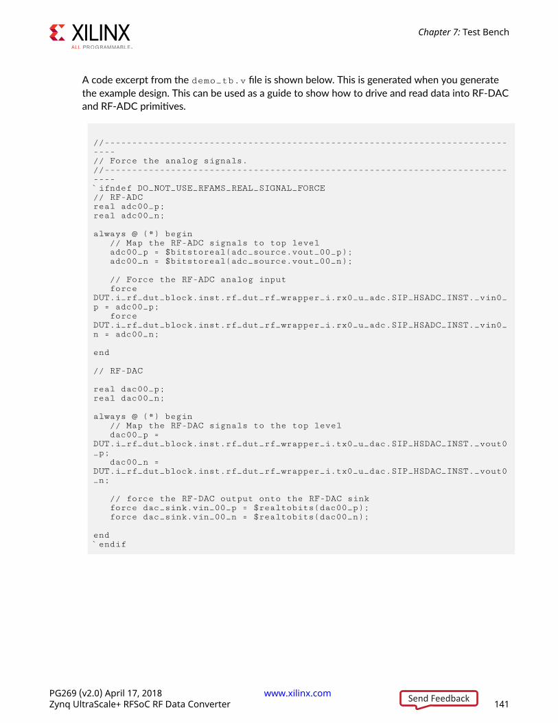
A code excerpt from the demo_tb.v file is shown below. This is generated when you generatethe example design. This can be used as a guide to show how to drive and read data into RF-DACand RF-ADC primitives.
//-----------------------------------------------------------------------------// Force the analog signals.//-----------------------------------------------------------------------------`ifndef DO_NOT_USE_RFAMS_REAL_SIGNAL_FORCE// RF-ADCreal adc00_p;real adc00_n;
always @ (*) begin // Map the RF-ADC signals to top level adc00_p = $bitstoreal(adc_source.vout_00_p); adc00_n = $bitstoreal(adc_source.vout_00_n); // Force the RF-ADC analog input force DUT.i_rf_dut_block.inst.rf_dut_rf_wrapper_i.rx0_u_adc.SIP_HSADC_INST._vin0_p = adc00_p; force DUT.i_rf_dut_block.inst.rf_dut_rf_wrapper_i.rx0_u_adc.SIP_HSADC_INST._vin0_n = adc00_n;
end
// RF-DAC
real dac00_p;real dac00_n;
always @ (*) begin // Map the RF-DAC signals to the top level dac00_p = DUT.i_rf_dut_block.inst.rf_dut_rf_wrapper_i.tx0_u_dac.SIP_HSDAC_INST._vout0_p; dac00_n = DUT.i_rf_dut_block.inst.rf_dut_rf_wrapper_i.tx0_u_dac.SIP_HSDAC_INST._vout0_n; // force the RF-DAC output onto the RF-DAC sink force dac_sink.vin_00_p = $realtobits(dac00_p); force dac_sink.vin_00_n = $realtobits(dac00_n); end`endif
Chapter 7: Test Bench
PG269 (v2.0) April 17, 2018 www.xilinx.com [placeholder text]Zynq UltraScale+ RFSoC RF Data Converter 141Send Feedback

Appendix A
Upgrading
Changes from V1.2 to V2.0Port Changes
Separate RF-ADC and RF-DAC versions of the user_sysref port have been added. Thischange affects cores with multi-tile synchronization enabled.
Table 53: Port Changes in Version 2.0
Port Direction Upgrade Actionuser_sysref_adc In Connect to user_sysref, if required
user_sysref_dac In Connect to user_sysref, if required
Changes from V1.1 to V1.2Port Changes
When the RF-ADC real-time signals are enabled the ports in the following table have beenadded.
Table 54: Port Changes in Version 1.2
Port Direction Upgrade Action2 GSPS RF-ADC1
adcXZ_over_range Out Leave open
adcXZ_over_voltage Out Leave open
4 GSPS RF-ADC2
adcX_ZZ_over_range Out Leave open
Appendix A: Upgrading
PG269 (v2.0) April 17, 2018 www.xilinx.com [placeholder text]Zynq UltraScale+ RFSoC RF Data Converter 142Send Feedback

Table 54: Port Changes in Version 1.2 (cont'd)
Port Direction Upgrade ActionadcX_ZZ_over_voltage Out Leave open
Notes:
1. X refers to the location of the tile in the converter column. Z refers to the location of the RF-ADC in the tile (0 to 3).2. X refers to the location of the tile in the converter column. ZZ is either 01 (the lower RF-ADC in the tile) or 23 (the
upper RF-ADC in the tile)
When the RF-ADC real-time signals are enabled the ports in the following table have beenrenamed.
Table 55: Ports Renamed in Version 1.2
Port Previous Name (v1.1) Direction Upgrade Action2 GSPS RF-ADC1
adcXZ_over_threshold1 adcXY_over_threshold1 Out Leave open
adcXZ_over_threshold2 adcXY_over_threshold2 Out Leave open
4 GSPS RF-ADC2
adcX_ZZ_over_threshold1 adcXY_over_threshold1 Out Leave open
adcX_ZZ_over_threshold2 adcXY_over_threshold2 Out Leave open
Notes:
1. X refers to the location of the tile in the converter column. Y refers to the location of the DDC block in the tile (0 to 3).Z refers to the location of the RF-ADC in the tile (0 to 3).
2. X refers to the location of the tile in the converter column. Y refers to the location of the DDC block in the tile (0 to 3).ZZ is either 01 (the lower RF-ADC in the tile) or 23 (the upper RF-ADC in the tile).
Parameter Changes
There are no parameter changes.
Appendix A: Upgrading
PG269 (v2.0) April 17, 2018 www.xilinx.com [placeholder text]Zynq UltraScale+ RFSoC RF Data Converter 143Send Feedback

Appendix B
DebuggingThis appendix includes details about resources available on the Xilinx Support website anddebugging tools.
Finding Help on Xilinx.comTo help in the design and debug process when using the core, the Xilinx Support web pagecontains key resources such as product documentation, release notes, answer records,information about known issues, and links for obtaining further product support.
DocumentationThis product guide is the main document associated with the core. This guide, along withdocumentation related to all products that aid in the design process, can be found on the XilinxSupport web page or by using the Xilinx® Documentation Navigator. Download the XilinxDocumentation Navigator from the Downloads page. For more information about this tool andthe features available, open the online help after installation.
Answer RecordsAnswer Records include information about commonly encountered problems, helpful informationon how to resolve these problems, and any known issues with a Xilinx product. Answer Recordsare created and maintained daily ensuring that users have access to the most accurateinformation available.
Answer Records for this core can be located by using the Search Support box on the main Xilinxsupport web page. To maximize your search results, use keywords such as:
• Product name
• Tool message(s)
• Summary of the issue encountered
A filter search is available after results are returned to further target the results.
Appendix B: Debugging
PG269 (v2.0) April 17, 2018 www.xilinx.com [placeholder text]Zynq UltraScale+ RFSoC RF Data Converter 144Send Feedback
Master Answer Record for the Core
AR 69907.
Technical SupportXilinx provides technical support in the Xilinx Support web page for this LogiCORE™ IP productwhen used as described in the product documentation. Xilinx cannot guarantee timing,functionality, or support if you do any of the following:
• Implement the solution in devices that are not defined in the documentation.
• Customize the solution beyond that allowed in the product documentation.
• Change any section of the design labeled DO NOT MODIFY.
To contact Xilinx Technical Support, navigate to the Xilinx Support web page.
Debug ToolsThere are many tools available to address Zynq® UltraScale+® RF Data Converter design issues.It is important to know which tools are useful for debugging various situations.
Vivado Design Suite Debug FeatureThe Vivado® Design Suite debug feature inserts logic analyzer and virtual I/O cores directly intoyour design. The debug feature also allows you to set trigger conditions to capture applicationand integrated block port signals in hardware. Captured signals can then be analyzed. Thisfeature in the Vivado IDE is used for logic debugging and validation of a design running in Xilinx®
devices.
The Vivado logic analyzer is used to interact with the logic debug LogiCORE IP cores, including:
• ILA 2.0 (and later versions)
• VIO 2.0 (and later versions)
See the Vivado Design Suite User Guide: Programming and Debugging (UG908).
Appendix B: Debugging
PG269 (v2.0) April 17, 2018 www.xilinx.com [placeholder text]Zynq UltraScale+ RFSoC RF Data Converter 145Send Feedback

Hardware DebugHardware issues can range from link bring-up to problems seen after hours of testing. Thissection provides debug steps for common issues. The Vivado® debug feature is a valuableresource to use in hardware debug. The signal names mentioned in the following individualsections can be probed using the debug feature for debugging the specific problems.
General ChecksEnsure that all the timing constraints for the core were properly incorporated from the exampledesign and that all constraints were met during implementation.
• Does it work in post-place and route timing simulation? If problems are seen in hardware butnot in timing simulation, this could indicate a PCB issue. Ensure that all clock sources areactive and clean.
• If using MMCMs in the design, ensure that all MMCMs have obtained lock by monitoring thelocked port.
• If your outputs go to 0, check your licensing.
Interface DebugAXI4-Lite InterfacesRead from a register that does not have all 0s as a default to verify that the interface isfunctional. Output s_axi_arready asserts when the read address is valid, and outputs_axi_rvalid asserts when the read data/response is valid. If the interface is unresponsive,ensure that the following conditions are met:
• The s_axi_aclk and aclk inputs are connected and toggling.
• The interface is not being held in reset, and s_axi_areset is an active-Low reset.
• The interface is enabled, and s_axi_aclken is active-High (if used).
• The main core clocks are toggling and that the enables are also asserted.
• If the simulation has been run, verify in simulation and/or a debug feature capture that thewaveform is correct for accessing the AXI4-Lite interface.
Appendix B: Debugging
PG269 (v2.0) April 17, 2018 www.xilinx.com [placeholder text]Zynq UltraScale+ RFSoC RF Data Converter 146Send Feedback

AXI4-Stream InterfacesIf data is not being transmitted or received, check the following conditions:
• If transmit <interface_name>_tready is stuck Low following the<interface_name>_tvalid input being asserted, the core cannot send data.
• If the receive <interface_name>_tvalid is stuck Low, the core is not receiving data.
• Check that the aclk inputs are connected and toggling.
• Check that the AXI4-Stream waveforms are being followed.
• Check core configuration.
Related InformationInterfacing to the AXI4-Stream Interface
Appendix B: Debugging
PG269 (v2.0) April 17, 2018 www.xilinx.com [placeholder text]Zynq UltraScale+ RFSoC RF Data Converter 147Send Feedback

Appendix C
Zynq UltraScale+ RFSoC DataConverter Bare-metal/Linux Driver
OverviewThe RFdc driver API functions for the Zynq® UltraScale+™ RFSoC RF Data Converter aredescribed in this chapter. The same driver is used for both bare metal and Linux. The driver forboth software platforms runs on the libmetal software layer provided by Xilinx. The driver iscomposed of the following files:
• API
xrfdc.c: The user interface API functions are implemented in this file.
xrfdc.h: The user interface API prototypes are provided in this file. The file providesprototypes of the driver instance structure and all other structures used across the APIs.The file implements utility in-line functions to access various data in the driver and IP.
xrfdc_mts.c: The multi-tile synchronization API functions are implemented in this file.
xrfdc_mts.h: The multi-tile synchronization API prototypes are provided in this file.
• Hardware Register Map
xrfdc_hw.h: Definitions for the hardware register maps are provided in this file. The filealso provides masks for various relevant fields for the Zynq UltraScale+ RFSoC registerinterface.
• Interrupt Handling
xrfdc_intr.c: Implements functions for the handling of various interrupts and errorsfrom the IP core.
Appendix C: Zynq UltraScale+ RFSoC Data Converter Bare-metal/Linux Driver
PG269 (v2.0) April 17, 2018 www.xilinx.com [placeholder text]Zynq UltraScale+ RFSoC RF Data Converter 148Send Feedback
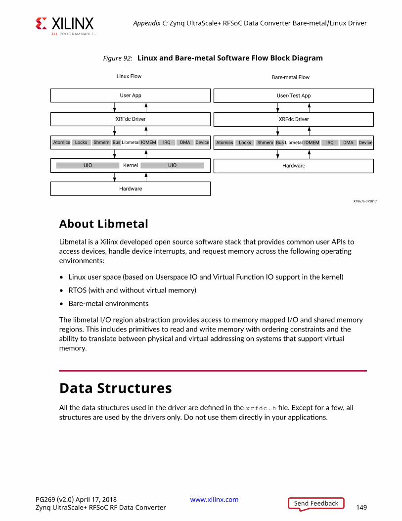
Figure 92: Linux and Bare-metal Software Flow Block Diagram
User App
XRFdc Driver
LibmetalAtomics Locks Shmem Bus IOMEM IRQ DMA Device
KernelUIO UIO
Hardware
User/Test App
XRFdc Driver
LibmetalAtomics Locks Shmem Bus IOMEM IRQ DMA Device
Hardware
Linux Flow Bare-metal Flow
X18675-032718X18676-072817
About LibmetalLibmetal is a Xilinx developed open source software stack that provides common user APIs toaccess devices, handle device interrupts, and request memory across the following operatingenvironments:
• Linux user space (based on Userspace IO and Virtual Function IO support in the kernel)
• RTOS (with and without virtual memory)
• Bare-metal environments
The libmetal I/O region abstraction provides access to memory mapped I/O and shared memoryregions. This includes primitives to read and write memory with ordering constraints and theability to translate between physical and virtual addressing on systems that support virtualmemory.
Data StructuresAll the data structures used in the driver are defined in the xrfdc.h file. Except for a few, allstructures are used by the drivers only. Do not use them directly in your applications.
Appendix C: Zynq UltraScale+ RFSoC Data Converter Bare-metal/Linux Driver
PG269 (v2.0) April 17, 2018 www.xilinx.com [placeholder text]Zynq UltraScale+ RFSoC RF Data Converter 149Send Feedback

struct XRFdc_PLL_SettingsThis structure is for internal driver use.
u32 Enabled; double RefClkFreq;double SampleRate;u32 RefClkDivider;u32 FeedbackDivider;u32 OutputDivider;u32 FractionalMode; u64 FractionalData; u32 FractWidth;
Description
• u32 Enabled: Indicates if the PLL is enabled (1) or disabled (0).
• double RefClkFreq: Reference clock frequency (MHz).
• double SampleRate: Sampling rate (GHz).
• u32 RefClkDivider: Reference clock divider.
• u32 FeedbackDivider: Feedback divider.
• u32 OutputDivider: Output divider.
• u32 FractionalMode: Fractional mode.
• u64 FractionalData: Fractional part of the feedback divider.
• u32 FractWidth: Fractional data width.
struct XRFdc_QMC_SettingsThis structure is used to set or get the QMC settings.
u32 EnablePhase;u32 EnableGain;double GainCorrectionFactor;double PhaseCorrectionFactor;s32 OffsetCorrectionFactor;u32 EventSource;
Description
• u32 EnablePhase: Indicates if phase is enabled (1) or disabled (0).
• u32 EnableGain: Indicates if gain is enabled(1) or disabled (0).
• double GainCorrectionFactor: Gain correction factor. Range: 0 to 2.0.
Appendix C: Zynq UltraScale+ RFSoC Data Converter Bare-metal/Linux Driver
PG269 (v2.0) April 17, 2018 www.xilinx.com [placeholder text]Zynq UltraScale+ RFSoC RF Data Converter 150Send Feedback

• double PhaseCorrectionFactor: Phase correction factor. Range: +/- 26.5 degrees.
• s32 OffsetCorrectionFactor: Offset correction factor is adding a fixed LSB value to thesampled signal.
• u32 EventSource: Event source for QMC settings. XRFDC_EVNT_SRC_* represents validvalues.
struct XRFdc_CoarseDelay_SettingsThis structure is used to set or get coarse delay settings.
u32 CoarseDelay;u32 EventSource;
Description
• u32 CoarseDelay: Coarse delay in the number of samples. Range: 0 to 7.
• u32 EventSource: Event source for coarse delay settings. XRFDC_EVNT_SRC_* representsvalid values.
struct XRFdc_Mixer_SettingsThis structure is used to set or get mixer settings.
double Freq;double PhaseOffset;u32 EventSource;u32 FineMixerMode;u32 CoarseMixFreq;u8 FineMixerScale;u32 CoarseMixMode;
Description
• double Freq: NCO frequency. Range: -Fs/2 to Fs/2 (GHz).
• double PhaseOffset: NCO phase offset. Range: -180 to 180.
• u32 EventSource: Event source for mixer settings. XRFDC_EVNT_SRC_* represents validvalues.
• u32 FineMixerMode: Mixer mode for fine mixer. XRFDC_FINE_MIXER_MOD_* representsvalid values.
• u32 CoarseMixFreq: Coarse mixer frequency. XRFDC_COARSE_MIX_* represents validvalues.
Appendix C: Zynq UltraScale+ RFSoC Data Converter Bare-metal/Linux Driver
PG269 (v2.0) April 17, 2018 www.xilinx.com [placeholder text]Zynq UltraScale+ RFSoC RF Data Converter 151Send Feedback

• u8 FineMixerScale: NCO output scale. XRFDC_MIXER_SCALE_* represents valid values.
• u32 CoarseMixMode: Mixer mode for coarse mixer. XRFDC_COARSE_MIX_MODE_*represents valid values.
struct XRFdc_Threshold_SettingsThis structure is used to set or get RF-ADC threshold settings.
u32 UpdateThreshold;u32 ThresholdMode[2];u32 ThresholdAvgVal[2];u32 ThresholdUnderVal[2];u32 ThresholdOverVal[2];
Description
• u32 UpdateThreshold: Selects which threshold to update. XRFDC_UPDATE_THRESHOLD_*represents valid values.
• u32 ThresholdMode[2]: Entry 0 is for Threshold0 and 1 for Threshold1. Range: 0 to 3 (0-OFF,1-sticky-over, 2-sticky-under and 3-hysteresis)
• u32 ThresholdAvgVal[2]: Threshold average value. Entry 0 is for Threshold0 and 1 forThreshold1.
• u32 ThresholdUnderVal[2]: Under threshold value. Entry 0 is for Threshold0 and 1 forThreshold1.
• u32 ThresholdOverVal[2]: Over threshold value. Entry 0 is for Threshold0 and 1 forThreshold1.
struct XRFdc_TileStatusThis structure is for internal driver use.
u32 IsEnabled;u32 TileState;u8 BlockStatusMask;u32 PowerUpState;u32 PLLState;
Description
• u32 IsEnabled: Indicates tile is enabled (1) or disabled (0).
• u32 TileState: Indicates current tile state.
• u8 BlockStatusMask: Bit mask for converter status. 1 indicates converter enable.
Appendix C: Zynq UltraScale+ RFSoC Data Converter Bare-metal/Linux Driver
PG269 (v2.0) April 17, 2018 www.xilinx.com [placeholder text]Zynq UltraScale+ RFSoC RF Data Converter 152Send Feedback

• u32 PowerUpState: Indicates power-up status.
• u32 PLLState: Indicates if PLL is locked or unlocked.
struct XRFdc_IPStatusThis structure is used to get the IP core status.
XRFdc_TileStatus DACTileStatus[4];XRFdc_TileStatus ADCTileStatus[4];u32 State;
Description
• XRFdc_TileStatus DACTileStatus[4]: Tile status for four RF-DAC tiles.
• XRFdc_TileStatus ADCTileStatus[4]: Tile status for four RF-ADC tiles.
• u32 State: Not currently supported.
struct XRFdc_BlockStatusThis structure is used to get the status of RF-DACs or RF-ADCs.
double SamplingFreq;u32 AnalogDataPathStatus;u32 DigitalDataPathStatus;u8 DataPathClocksStatus; u8 IsFIFOFlagsEnabled;u8 IsFIFOFlagsAsserted;
Description
• double SamplingFreq: Sampling frequency.
• u32 AnalogDataPathStatus:
• RF-ADC
bit[0] Converter enable/disable.
• RF-DAC
[3:0] Inverse sinc enable/disable.
[7:4] Decoder mode.
• u32 DigitalDataPathStatus:
Appendix C: Zynq UltraScale+ RFSoC Data Converter Bare-metal/Linux Driver
PG269 (v2.0) April 17, 2018 www.xilinx.com [placeholder text]Zynq UltraScale+ RFSoC RF Data Converter 153Send Feedback

• RF-ADC
[3:0] FIFO status (enable/disable).
[7:4] Decimation factor.
[11:8] Mixer mode.
• RF-DAC
[3:0] FIFO status.
[7:4] Interpolation factor.
[11:8] Adder status.
[15:12] Mixer mode.
• u8 DataPathClocksStatus: Indicates if all required datapath clocks are enabled; 1 if all clocksenabled, 0 otherwise.
• u8 IsFIFOFlagsEnabled: FIFO flags enabled mask; 1 is enabled, otherwise 0.
• u8 IsFIFOFlagsAsserted: FIFO flags asserted mask; 1 is enabled, otherwise 0.
struct XRFdc_DACBlock_AnalogDataPath_ConfigThis structure is for internal driver use.
u32 BlockAvailable;u32 InvSyncEnable;u32 MixMode;u32 DecoderMode;
Description
• u32 BlockAvailable: Corresponds to the C_DAC_Slicexy_Enable IP parameter.
• u32 InvSyncEnable: Corresponds to the C_DAC_Invsinc_Ctrlxy IP parameter.
• u32 MixMode: Corresponds to the C_DAC_Mixer_Modexy IP parameter.
• u32 DecoderMode: Corresponds to the C_DAC_Decoder_Modexy IP parameter.
Appendix C: Zynq UltraScale+ RFSoC Data Converter Bare-metal/Linux Driver
PG269 (v2.0) April 17, 2018 www.xilinx.com [placeholder text]Zynq UltraScale+ RFSoC RF Data Converter 154Send Feedback

struct XRFdc_DACBlock_DigitalDataPath_ConfigThis structure is for internal driver use.
u32 DataType;u32 DataWidth;u32 InterpolationMode;u32 FifoEnable;u32 AdderEnable;
Description
• u32 DataType: Corresponds to the C_DAC_Data_Typexy IP parameter.
• u32 DataWidth: Corresponds to the C_DAC_Data_Widthxy IP parameter.
• u32 InterpolationMode: Corresponds to the C_DAC_Interpolation_Modexy IPparameter.
• u32 FifoEnable: Corresponds to the C_DAC_Fifoxy IP parameter.
• u32 AdderEnable: Corresponds to the C_DAC_Adderxy IP parameter.
struct XRFdc_ADCBlock_AnalogDataPath_ConfigThis structure is for internal driver use.
u32 BlockAvailable;u32 MixMode;
Description
• u32 BlockAvailable: Corresponds to the C_ADC_Slicexy_Enable IP parameter.
• u32 MixMode: Corresponds to the C_ADC_Mixer_Modexy IP parameter.
struct XRFdc_ADCBlock_DigitalDataPath_ConfigThis structure is for internal driver use.
u32 DataType;u32 DataWidth;u32 DecimationMode;u32 FifoEnable;
Appendix C: Zynq UltraScale+ RFSoC Data Converter Bare-metal/Linux Driver
PG269 (v2.0) April 17, 2018 www.xilinx.com [placeholder text]Zynq UltraScale+ RFSoC RF Data Converter 155Send Feedback

Description
• u32 DataType: Corresponds to the C_ADC_Data_Typexy IP parameter.
• u32 DataWidth: Corresponds to the C_ADC_Data_Widthxy IP parameter.
• u32 DecimationMode: Corresponds to the C_ADC_Decimation_Modexy IP parameter.
• u32 FifoEnable: Corresponds to the C_ADC_Fifoxy IP parameter.
struct XRFdc_DACTile_ConfigThis structure is for internal driver use.
u32 Enable;u32 PLLEnable;double SamplingRate; double RefClkFreq;double FabClkFreq;XRFdc_DACBlock_AnalogDataPath_Config DACBlock_Analog_Config[4];XRFdc_DACBlock_DigitalDataPath_Config DACBlock_Digital_Config[4];
Description
• u32 Enable: Corresponds to the C_DACx_Enable IP parameter.
• u32 PLLEnable: Corresponds to the C_DACx_PLL_Enable IP parameter.
• double SamplingRate: Corresponds to the C_DACx_Sampling_Rate IP parameter.
• double RefClkFre: Corresponds to the C_DACx_RefClk_Freq IP parameter.
• double FabClkFreq: Corresponds to the C_DACx_FabClk_Freq IP parameter.
struct XRFdc_ADCTile_ConfigThis structure is for internal driver use.
u32 Enable;u32 PLLEnable;double SamplingRatedouble RefClkFreq; double FabClkFreq;XRFdc_ADCBlock_AnalogDataPath_Config ADCBlock_AnalogConfig[4];XRFdc_ADCBlock_DigitalDataPath_Config ADCBlock_Digital_Config[4];
Description
• u32 Enable: Corresponds to the C_ADCx_Enable IP parameter.
• u32 PLLEnable: Corresponds to the C_ADCx_PLL_Enable IP parameter.
Appendix C: Zynq UltraScale+ RFSoC Data Converter Bare-metal/Linux Driver
PG269 (v2.0) April 17, 2018 www.xilinx.com [placeholder text]Zynq UltraScale+ RFSoC RF Data Converter 156Send Feedback

• double SamplingRate: Corresponds to the C_ADCx_Sampling_Rate IP parameter.
• double RefClkFreq: Corresponds to the C_ADCx_RefClk_Freq IP parameter.
• double FabClkFreq: Corresponds to the C_ADCx_FabClk_Freq IP parameter.
struct XRFdc_ConfigThis structure is for internal driver use (metal_phys_addr_t represents unsigned long).
u32 DeviceId;#ifndef _MICROBLAZE_ metal_phys_addr_t BaseAddr;#else u32 BaseAddr;#endif /* IP Base Address */u32 ADCType;u32 MasterADCTile;u32 MasterDACTile;u32 ADCSysRefSource;u32 DACSysRefSource;XRFdc_DACTile_Config DACTile_Config[4];XRFdc_ADCTile_Config ADCTile_Config[4];
Description
• u32 ADCType: 2 GSPS RF-ADC part or 4 GSPS RF-ADC part.
• u32 MasterADCTile: Corresponds to the C_ADC_Master IP parameter.
• u32 MasterDACTile : Corresponds to the C_DAC_Master IP parameter.
• u32 ADCSysRefSource : Corresponds to the C_ADC_Sysref_Source IP parameter.
• u32 DACSysRefSource: Corresponds to the C_DAC_Sysref_Source IP parameter.
struct XRFdc_DACBlock_AnalogDataPathThis structure is for internal driver use.
u32 Enabled;u32 MixedMode;double TerminationVoltage;double OutputCurrent;u32 InverseSincFilterEnable;u32 DecoderMode;void * FuncHandler;XRFdc_QMC_Settings QMC_Settings;XRFdc_CoarseDelay_Settings CoarseDelay_Settings;u32 NyquistZone;
Appendix C: Zynq UltraScale+ RFSoC Data Converter Bare-metal/Linux Driver
PG269 (v2.0) April 17, 2018 www.xilinx.com [placeholder text]Zynq UltraScale+ RFSoC RF Data Converter 157Send Feedback

Description
• u32 Enabled: RF-DAC enable (1) or disable (0).
• u32 MixedMode: Mixer mode.
• double TerminationVoltage: Termination voltage.
• double OutputCurrent: Output current.
• u32 InverseSincFilterEnable: Inverse sinc filter enable (1) or disable (0).
• u32 DecoderMode: Decoder mode.
• void * FuncHandler: Function handler (currently not used in the driver).
• XRFdc_QMC_Settings QMC_Settings: QMC settings structure.
• XRFdc_CoarseDelay_Settings CoarseDelay_Settings: CoarseDelay settings structure.
• u32 NyquistZone: Nyquist zone.
struct XRFdc_DACBlock_DigitalDataPathThis structure is for internal driver use.
u32 DataType; u32 DataWidth;int ConnectedIData;int ConnectedQData;u32 InterpolationFactor; XRFdc_Mixer_Settings Mixer_Settings;
Description
• u32 DataType: Digital input datatype.
• u32 DataWidth: Data width (samples per AXI4-Stream word).
• int ConnectedIData: Data converter connected for I datapath. Valid values are 0-3 and -1.
• int ConnectedQData: Data converter connected for Q datapath. Valid values are 0-3 and -1.
• u32 InterpolationFactor: Interpolation factor.
• XRFdc_Mixer_Settings Mixer_Settings: Mixer settings structure.
Appendix C: Zynq UltraScale+ RFSoC Data Converter Bare-metal/Linux Driver
PG269 (v2.0) April 17, 2018 www.xilinx.com [placeholder text]Zynq UltraScale+ RFSoC RF Data Converter 158Send Feedback
struct XRFdc_ADCBlock_AnalogDataPathThis structure is for internal driver use.
u32 Enabled; XRFdc_QMC_Settings QMC_Settings;XRFdc_CoarseDelay_Settings CoarseDelay_Settings;XRFdc_Threshold_Settings Threshold_Settings;u32 NyquistZone;u8 CalibrationMode;
Description
• u32 Enabled: RF-ADC Enable (1) or Disable (0).
• XRFdc_QMC_Settings QMC_Settings: QMC settings structure.
• XRFdc_CoarseDelay_Settings CoarseDelay_Settings: Coarse delay settings structure.
• XRFdc_Threshold_Settings Threshold_Settings: Threshold settings structure.
• u32 NyquistZone: Nyquist zone.
• u8 CalibrationMode: Calibration mode, set by the XRFdc_SetCalibrationMode APIfunction.
struct XRFdc_ADCBlock_DigitalDataPathThis structure is for internal driver use.
u32 DataType;u32 DataWidth;u32 DecimationFactor;int ConnectedIData;int ConnectedQData;XRFdc_Mixer_Settings Mixer_Settings;
Description
• u32 DataType: Analog input data type.
• u32 DataWidth: Data width (samples per AXI4-Stream word).
• u32 DecimationFactor: Decimation factor.
• int ConnectedIData: Data converter connected for I datapath. Valid values are 0-3 and -1.
• int ConnectedQData: Data converter connected for Q datapath. Valid values are 0-3 and -1.
• XRFdc_Mixer_Settings Mixer_Settings: Mixer settings structure.
Appendix C: Zynq UltraScale+ RFSoC Data Converter Bare-metal/Linux Driver
PG269 (v2.0) April 17, 2018 www.xilinx.com [placeholder text]Zynq UltraScale+ RFSoC RF Data Converter 159Send Feedback

struct XRFdc_DAC_TileThis structure is for internal driver use.
u32 TileBaseAddr;u32 NumOfDACBlocks;XRFdc_PLL_Settings PLL_Settings;XRFdc_DACBlock_AnalogDataPath DACBlock_Analog_Datapath[4];XRFdc_DACBlock_DigitalDataPath DACBlock_Digital_Datapath[4];
Description
• u32 TileBaseAddr: Tile base address.
• u32 NumOfDACBlocks: Number of RF-DACs enabled.
• XRFdc_PLL_Settings PLL_Settings: PLL settings structure.
• XRFdc_DACBlock_AnalogDataPath DACBlock_Analog_Datapath[4]:DACBlock_AnalogDataPath structure for four RF-DACs.
• XRFdc_DACBlock_DigitalDataPath DACBlock_Digital_Datapath[4]:DACBlock_DigitalDataPath structure for four RF-DACs.
struct XRFdc_ADC_TileThis structure is for internal driver use.
u32 TileBaseAddr;u32 NumOfADCBlocks; XRFdc_PLL_Settings PLL_Settings;XRFdc_ADCBlock_AnalogDataPath ADCBlock_Analog_Datapath[4];XRFdc_ADCBlock_DigitalDataPath ADCBlock_Digital_Datapath[4];
Description
• u32 TileBaseAddr: Tile base address.
• u32 NumOfADCBlocks: Number of RF-ADCs enabled.
• XRFdc_PLL_Settings PLL_Settings: PLL settings structure.
• XRFdc_ADCBlock_AnalogDataPath ADCBlock_Analog_Datapath[4]:ADCBlock_AnalogDataPath structure for four RF-ADCs.
• XRFdc_ADCBlock_DigitalDataPath ADCBlock_Digital_Datapath[4]:ADCBlock_DigitalDataPath structure for four RF-ADCs.
Appendix C: Zynq UltraScale+ RFSoC Data Converter Bare-metal/Linux Driver
PG269 (v2.0) April 17, 2018 www.xilinx.com [placeholder text]Zynq UltraScale+ RFSoC RF Data Converter 160Send Feedback

struct XRFdc //Driver instance structureThis structure is for internal driver use.
XRFdc_Config RFdc_Config;u32 IsReady;u32 ADC4GSPS;#ifndef __MICROBLAZE__ metal_phys_addr_t BaseAddr; struct metal_io_region *io; struct metal_device *device;#else u32 BaseAddr;#endifXRFdc_DAC_Tile DAC_Tile[4];XRFdc_ADC_Tile ADC_Tile[4];XRFds_StatusHandler StatusHandler;void *CallBackRef; u8 UpdateMixerScale;
Description
• XRFdc_Config RFdc_Config: Driver structure configuration.
• u32 IsReady: This flag is used to indicate that the driver is ready.
• u32 ADC4GSPS: This flag is used to indicate if RF-ADC is 4 GSPS.
• metal_phys_addr_t BaseAddr: Base address.
• struct metal_io_region: Libmetal IO structure.
• struct metal_device *device: Libmetal device structure.
• XRFdc_DAC_Tile DAC_Tile[4]: RF-DAC tile structure for four tiles.
• XRFdc_ADC_Tile ADC_Tile[4]: RF-ADC tile structure for four tiles.
• XRFds_StatusHandler StatusHandler: Event handler function.
• void *CallBackRef: Callback reference for event handler.
• u8 UpdateMixerScale: Set to 1 to overwrite mixer scale.
Appendix C: Zynq UltraScale+ RFSoC Data Converter Bare-metal/Linux Driver
PG269 (v2.0) April 17, 2018 www.xilinx.com [placeholder text]Zynq UltraScale+ RFSoC RF Data Converter 161Send Feedback

struct XRFdc_MultiConverter_Sync_ConfigThis structure is used to configure the MTS algorithm. Indicated files can be configured in thecode.
u32 RefTile;u32 Tiles;int Target_Latency;int Offset[4];int Latency[4];int Marker_Delay;int SysRef_Enable;XRFdc_MTS_DTC_Settings DTC_Set_PLL;XRFdc_MTS_DTC_Settings DTC_Set_T1;
Description
• u32 RefTile: Reference tile (must be 0).
• u32 Tiles: Bitmask indicating which tiles to align. BitX enables MTS for TileX. Tile0 mustalways be enabled.
• int Target_Latency: Sets the target relative latency. This is required to be set for multi-chipalignment, or deterministic latency use-cases. It is not required to be set for single-chipalignment.
• int Offset[4]: Status – indicates the value the interface data was delayed by to achievealignment, per tile.
• int Latency[4]: Status – indicates the measured relative-latency value of each tile.
• int Marker_Delay: Marker delay is for internal use.
• int SysRef_Enable: Set to 1 (default) to keep SYSREF capture enabled after MTS runs. Set to 0to disable SYSREF capture.
struct XRFdc_MTS_MarkerThis structure is for internal driver use. There are no user-configurable fields.
u32 Count[4];u32 Loc[4];
Appendix C: Zynq UltraScale+ RFSoC Data Converter Bare-metal/Linux Driver
PG269 (v2.0) April 17, 2018 www.xilinx.com [placeholder text]Zynq UltraScale+ RFSoC RF Data Converter 162Send Feedback

struct XRFdc_MTS_DTC_SettingsThis structure is for internal driver use. There are no user-configurable fields.
u32 RefTile;u32 IsPLL;int Target[4];int Scan_Mode;int DTC_Code[4];int Num_Windows[4];int Max_Gap[4];int Min_Gap[4];int Max_Overlap[4];
User API FunctionsAll user API functions are implemented in the source file xrfdc.c. The prototypes for these areprovided in header file xrfdc.h.
All driver API functions have InstancePtr as an argument. It is a pointer to the XRFdcstructure that contains information about the base address, the structure pointing to RFdcdefault configurations, and structures for RF-ADC and RF-DAC tile configurations. TheInstancePtr argument is initialized in the XRFdc_CfgInitialize API function. Call theXRFdc_CfgInitialize API function to initialize InstancePtr before calling any otherfunctions.
XRFdc_CfgInitializeFunction Prototype
int XRFdc_CfgInitialize (XRFdc* InstancePtr, XRFdc_Config *Config);
Arguments
• XRFdc* InstancePtr: Pointer to the driver instance.
• XRFdc_Config *Config: Pointer to the configuration structure.
Description
This API function populates appropriate entries in the driver instance by copying relevant entriesfrom the configuration structure. This function is required for any software interaction with theRFdc driver API and must be called first before using any other API functions.
Appendix C: Zynq UltraScale+ RFSoC Data Converter Bare-metal/Linux Driver
PG269 (v2.0) April 17, 2018 www.xilinx.com [placeholder text]Zynq UltraScale+ RFSoC RF Data Converter 163Send Feedback
Return Value
XRFDC_SUCCESS
XRFDC_FAILURE
XRFdc_LookupConfigFunction Prototype
XRFdc_Config *XRFdc_LookupConfig(u16 DeviceId);
Arguments
• u16 DeviceId: ID of the device whose configuration information is required.
Description
This API function looks up the device configuration based on the unique ID of the device. A tablecontains the configuration information for each device in the system.
Return Value
The function returns a pointer to the configuration found, or NULL if the specified device ID wasnot found.
XRFdc_StartUpFunction Prototype
int XRFdc_StartUp (XRFdc* InstancePtr, u32 Type, int Tile_Id);
Arguments
• XRFdc* InstancePtr: Pointer to the driver instance.
• u32 Type: RF-ADC or RF-DAC; 0 for RF-ADC and 1 for RF-DAC.
• int Tile_Id: RF-ADC or RF-DAC; 0 for RF-ADC and 1 for RF-DAC.
Description
This API function restarts the tile as requested through Tile_Id. If -1 is passed as Tile_Id,the function restarts all the enabled tiles. Existing register settings are not lost or altered in theprocess.
Appendix C: Zynq UltraScale+ RFSoC Data Converter Bare-metal/Linux Driver
PG269 (v2.0) April 17, 2018 www.xilinx.com [placeholder text]Zynq UltraScale+ RFSoC RF Data Converter 164Send Feedback

Return Value
XRFDC_SUCCESS
XRFDC_FAILURE (returned when the tile is not enabled or available)
XRFdc_ShutdownFunction Prototype
int XRFdc_Shutdown (XRFdc* InstancePtr, u32 Type, int Tile_Id);
Arguments
• XRFdc* InstancePtr: Pointer to the driver instance.
• u32 Typ: RF-ADC or RF-DAC; 0 for RF-ADC and 1 for RF-DAC.
• int Tile_Id: Valid values are 0-3 and -1 (for all tiles).
Description
This API function stops the tile as requested through Tile_Id. If -1 is passed as Tile_Id, thefunction stops all the enabled tiles. The existing register settings are not cleared.Note: This is a common API function for RF-ADC and RF-DAC tiles.
Return Value
XRFDC_SUCCESS
XRFDC_FAILURE (returned when the tile is not enabled or available)
XRFdc_ResetFunction Prototype
int XRFdc_Reset (XRFdc* InstancePtr, u32 Type, int Tile_Id);
Arguments
• XRFdc* InstancePtr: Pointer to the driver instance.
• u32 Type: RF-ADC or RF-DAC; 0 for RF-ADC and 1 for RF-DAC.
• int Tile_Id: Valid values are 0-3 and -1 (for all tiles).
Appendix C: Zynq UltraScale+ RFSoC Data Converter Bare-metal/Linux Driver
PG269 (v2.0) April 17, 2018 www.xilinx.com [placeholder text]Zynq UltraScale+ RFSoC RF Data Converter 165Send Feedback

Description
This API function resets the tile as requested through Tile_Id. If -1 is passed as Tile_Id, itresets all the enabled tiles. All existing register settings are cleared and are replaced with thesettings initially configured.Note: This is a common API function for RF-ADC and RF-DAC tiles.
Return Value
XRFDC_SUCCESS
XRFDC_FAILURE (returned when the tile is not enabled or available)
XRFdc_RestartIPSMFunction Prototype
static void XRFdc_RestartIPSM (XRFdc* InstancePtr, u32 BaseAddress, u32 Start, u32 End);
Arguments
• XRFdc* InstancePtr: Pointer to the driver instance.
• u32 BaseAddress: Tile control and status register base address.
• u32 Start: Start state of state machine.
• int End: End state of state machine.
Description
This API function restarts the requested tile and ensures that it starts from a defined start stateand reaches the requested or defined end state. This function is for internal driver use.Note: This a common API function for both RF-ADC and RF-DAC tiles.
Return Value
None.
Appendix C: Zynq UltraScale+ RFSoC Data Converter Bare-metal/Linux Driver
PG269 (v2.0) April 17, 2018 www.xilinx.com [placeholder text]Zynq UltraScale+ RFSoC RF Data Converter 166Send Feedback

XRFdc_GetIPStatusFunction Prototype
int XRFdc_GetIPStatus (XRFdc* InstancePtr, XRFdc_IPStatus* IPStatus);
Arguments
• XRFdc* InstancePtr: Pointer to the driver instance.
• XRFdc_IPStatus* IPStatus: Pointer to the XRFdc_IPStatus structure through which thestatus is returned.
Description
This API function returns the IP status.
Return Value
XRFDC_SUCCESS
XRFDC_FAILURE (IP not ready)
XRFdc_GetBlockStatusFunction Prototype
int XRFdc_GetBlockStatus (XRFdc* InstancePtr, u32 Type, int Tile_Id, u32 Block_Id, XRFdc_BlockStatus* BlockStatus);
Arguments
• XRFdc* InstancePtr: Pointer to the driver instance.
• u32 Type: RF-ADC or RF-DAC; 0 for RF-ADC and 1 for RF-DAC.
• int Tile_Id: RF-ADC/RF-DAC tile number. Valid values are 0-3.
• u32 Block_Id: RF-ADC/RF-DAC block number inside the tile. Valid values are 0-3.
• XRFdc_BlockStatus * BlockStatus: Pointer to the XRFdc_BlockStatus structure through whichthe RF-ADC/RF-DAC block status is returned.
Description
This API function returns the requested block status.
Appendix C: Zynq UltraScale+ RFSoC Data Converter Bare-metal/Linux Driver
PG269 (v2.0) April 17, 2018 www.xilinx.com [placeholder text]Zynq UltraScale+ RFSoC RF Data Converter 167Send Feedback

Note: This is a common API function for RF-ADCs/RF-DACs.
Return Value
XRFDC_SUCCESS
XRFDC_FAILURE (Converter not enabled)
XRFdc_SetMixerSettingsFunction Prototype
int XRFdc_SetMixerSettings (XRFdc* InstancePtr, u32 Type, int Tile_Id, u32 Block_Id, XRFdc_Mixer_Settings * Mixer_Settings);
Arguments
• XRFdc* InstancePtr: Pointer to the driver instance.
• u32 Type: RF-ADC or RF-DAC; 0 for RF-ADC and 1 for RF-DAC.
• int Tile_Id: RF-ADC/RF-DAC tile number. Valid values are 0-3.
• u32 Block_Id: RF-ADC/RF-DAC number inside the tile. Valid values are 0-3.
• XRFdc_Mixer_Settings * Mixer_Settings: Pointer to the XRFdc_Mixer_Settings structurethat passes the mixer/NCO settings.
Description
Mixer/NCO settings passed are used to update the corresponding block level registers. Thedriver structure is updated with the new values.Note: This is a common API function for RF-ADCs/RF-DACs.
Return Value
XRFDC_SUCCESS
XRFDC_FAILURE
Appendix C: Zynq UltraScale+ RFSoC Data Converter Bare-metal/Linux Driver
PG269 (v2.0) April 17, 2018 www.xilinx.com [placeholder text]Zynq UltraScale+ RFSoC RF Data Converter 168Send Feedback
XRFdc_GetMixerSettingsFunction Prototype
int XRFdc_GetMixerSettings (XRFdc* InstancePtr, u32 Type, int Tile_Id, u32 Block_Id, XRFdc_Mixer_Settings * Mixer_Settings);
Arguments
• XRFdc* InstancePtr: Pointer to the driver instance.
• u32 Type: RF-ADC or RF-DAC; 0 for RF-ADC and 1 for RF-DAC.
• int Tile_Id: RF-ADC/RF-DAC tile number. Valid values are 0-3.
• u32 Block_Id: RF-ADC/RF-DAC number inside the tile. Valid values are 0-3.
• XRFdc_Mixer_Settings * Mixer_Settings: Pointer to the XRFdc_Mixer_Settings structurein which the existing mixer/NCO settings are returned.
Description
Mixer/NCO settings from corresponding registers are returned to the caller.Note: This is a common API function for RF-ADCs/RF-DACs.
Return Value
XRFDC_SUCCESS
XRFDC_FAILURE
XRFdc_SetQMCSettingsFunction Prototype
int XRFdc_SetQMCSettings (XRFdc* InstancePtr, u32 Type, int Tile_Id, u32 Block_Id, XRFdc_QMC_Settings * QMC_Settings);
Arguments
• XRFdc* InstancePtr: Pointer to the driver instance.
• u32 Type: RF-ADC or RF-DAC; 0 for RF-ADC and 1 for RF-DAC.
• int Tile_Id: RF-ADC/RF-DAC tile number. Valid values are 0-3.
Appendix C: Zynq UltraScale+ RFSoC Data Converter Bare-metal/Linux Driver
PG269 (v2.0) April 17, 2018 www.xilinx.com [placeholder text]Zynq UltraScale+ RFSoC RF Data Converter 169Send Feedback

• u32 Block_Id: RF-ADC/RF-DAC number inside the tile. Valid values are 0-3.
• XRFdc_QMC_Settings * QMC_Settings: Pointer to the XRFdc_QMC_Settings structure usedto update the corresponding registers.
Description
QMC settings from the passed structure are populated into the corresponding registers. Thedriver structure is updated with the new values.Note: This is a common API function for RF-ADCs/RF-DACs.
Return Value
XRFDC_SUCCESS
XRFDC_FAILURE
Related InformationThreshold RFdc Driver API Commands
XRFdc_GetQMCSettingsFunction Prototype
int XRFdc_GetQMCSettings (XRFdc* InstancePtr, u32 Type, int Tile_Id, u32 Block_Id, XRFdc_QMC_Settings * QMC_Settings);
Arguments
• XRFdc* InstancePtr: Pointer to the driver instance.
• u32 Type: RF-ADC or RF-DAC; 0 for RF-ADC and 1 for RF-DAC.
• int Tile_Id: RF-ADC/RF-DAC tile number. Valid values are 0-3.
• u32 Block_Id: RF-ADC/RF-DAC number inside the tile. Valid values are 0-3.
• XRFdc_QMC_Settings * QMC_Settings: Pointer to the XRFdc_QMC_Settings structure thatreturns the corresponding register values.
Description
QMC settings from the relevant registers are returned back to the caller.Note: This is a common API function for RF-ADCs/RF-DACs.
Appendix C: Zynq UltraScale+ RFSoC Data Converter Bare-metal/Linux Driver
PG269 (v2.0) April 17, 2018 www.xilinx.com [placeholder text]Zynq UltraScale+ RFSoC RF Data Converter 170Send Feedback

Return Value
XRFDC_SUCCESS
XRFDC_FAILURE
XRFdc_GetCoarseDelaySettingsFunction Prototype
int XRFdc_GetCoarseDelaySettings (XRFdc* InstancePtr, u32 Type, int Tile_Id, u32 Block_Id, XRFdc_CoarseDelay_Settings * CoarseDelay_Settings);
Arguments
• XRFdc* InstancePtr: Pointer to the driver instance.
• u32 Type: RF-ADC or RF-DAC; 0 for RF-ADC and 1 for RF-DAC.
• int Tile_Id: RF-ADC/RF-DAC tile number. Valid values are 0-3.
• u32 Block_Id: RF-ADC/RF-DAC number inside the tile. Valid values are 0-3.
• XRFdc_CoarseDelay_Settings * CoarseDelay_Settings: Pointer to theXRFdc_CoarseDelay_Settings structure which returns the corresponding registervalues.
Description
Coarse delay settings from the relevant registers are returned back to the caller.Note: This is a common API function for RF-ADCs/RF-DACs.
Return Value
XRFDC_SUCCESS
XRFDC_FAILURE
XRFdc_SetCoarseDelaySettingsFunction Prototype
int XRFdc_SetCoarseDelaySettings (XRFdc* InstancePtr, u32 Type, int Tile_Id, u32 Block_Id, XRFdc_CoarseDelay_Settings * CoarseDelay_Settings);
Appendix C: Zynq UltraScale+ RFSoC Data Converter Bare-metal/Linux Driver
PG269 (v2.0) April 17, 2018 www.xilinx.com [placeholder text]Zynq UltraScale+ RFSoC RF Data Converter 171Send Feedback

Arguments
• XRFdc* InstancePtr: Pointer to the driver instance.
• u32 Type: RF-ADC or RF-DAC; 0 for RF-ADC and 1 for RF-DAC.
• int Tile_Id: RF-ADC/RF-DAC tile number. Valid values are 0-3.
• u32 Block_Id: RF-ADC/RF-DAC number inside the tile. Valid values are 0-3.
• XRFdc_CoarseDelay_Settings * CoarseDelay_Settings: Pointer to theXRFdc_CoarseDelay_Settings structure through which the coarse delay settings arepassed.
Description
Coarse delay settings passed from the caller are updated in the relevant registers. The driverstructure is updated with the new values.Note: This is a common API function for RF-ADCs/RF-DACs.
Appendix C: Zynq UltraScale+ RFSoC Data Converter Bare-metal/Linux Driver
PG269 (v2.0) April 17, 2018 www.xilinx.com [placeholder text]Zynq UltraScale+ RFSoC RF Data Converter 172Send Feedback

Return Value
XRFDC_SUCCESS
XRFDC_FAILURE
XRFdc_UpdateEventFunction Prototype
int XRFdc_UpdateEvent (XRFdc* InstancePtr, u32 Type, int Tile_Id, u32 Block_Id, u32 Event);
Arguments
• XRFdc* InstancePtr: Pointer to the driver instance.
• u32 Type: RF-ADC or RF-DAC; 0 for RF-ADC and 1 for RF-DAC.
• int Tile_Id: RF-ADC/RF-DAC tile number. Valid values are 0-3.
• u32 Block_Id: RF-ADC/RF-DAC number inside the tile. Valid values are 0-3.
• u32 Event: Event can be mixer, QMC, or coarse delay.
Description
Use this function to trigger the update event for an event, if the event source is Slice or Tile.Note: This is a common API function for RF-ADCs/RF-DACs.
Return Value
XRFDC_SUCCESS
XRFDC_FAILURE
XRFdc_SetInterpolationFactorFunction Prototype
int XRFdc_SetInterpolationFactor (XRFdc* InstancePtr, int Tile_Id, u32 Block_Id, u32 InterpolationFactor);
Arguments
• XRFdc* InstancePtr: Pointer to the driver instance.
Appendix C: Zynq UltraScale+ RFSoC Data Converter Bare-metal/Linux Driver
PG269 (v2.0) April 17, 2018 www.xilinx.com [placeholder text]Zynq UltraScale+ RFSoC RF Data Converter 173Send Feedback

• int Tile_Id: RF-DAC tile number. Valid values are 0-3.
• u32 Block_Id: RF-DAC number. Valid values are 0-3.
• u32 InterpolationFactor: Interpolation factor to be set for the RF-DAC.
Description
This API function sets the interpolation factor for the requested RF-DAC and also updates theFIFO read width based on the interpolation factor.
Return Value
XRFDC_SUCCESS
XRFDC_FAILURE
XRFdc_GetInterpolationFactorFunction Prototype
int XRFdc_GetInterpolationFactor (XRFdc* InstancePtr, int Tile_Id, u32 Block_Id, u32 * InterpolationFactor);
Arguments
• XRFdc* InstancePtr: Pointer to the driver instance.
• int Tile_Id: RF-DAC tile number. Valid values are 0-3.
• u32 Block_Id: RF-DAC number inside the tile. Valid values are 0-3.
• u32 * InterpolationFactor: Pointer to return the interpolation factor for the RF-DAC.
Description
The interpolation factor for the requested RF-DAC is returned back to the caller.Note: This API function is only applicable for RF-DACs.
Return Value
XRFDC_SUCCESS
XRFDC_FAILURE
Appendix C: Zynq UltraScale+ RFSoC Data Converter Bare-metal/Linux Driver
PG269 (v2.0) April 17, 2018 www.xilinx.com [placeholder text]Zynq UltraScale+ RFSoC RF Data Converter 174Send Feedback

XRFdc_SetDecimationFactorFunction Prototype
int XRFdc_SetDecimationFactor (XRFdc* InstancePtr, int Tile_Id, u32 Block_Id, u32 DecimationFactor);
Arguments
• XRFdc* InstancePtr: Pointer to the driver instance.
• int Tile_Id: RF-ADC tile number. Valid values are 0-3.
• u32 Block_Id: RF-ADC number. Valid values are 0-3.
• u32 DecimationFactor: Decimation factor to be set for the RF-ADC.
Description
This API function sets the decimation factor for the requested RF-ADC and also updates theFIFO write width based on the decimation factor.Note: This function is only applicable for RF-ADCs.
Return Value
XRFDC_SUCCESS
XRFDC_FAILURE
XRFdc_GetDecimationFactorFunction Prototype
int XRFdc_GetDecimationFactor (XRFdc* InstancePtr, int Tile_Id, u32 Block_Id, u32 * DecimationFactor);
Arguments
• XRFdc* InstancePtr: Pointer to the driver instance.
• int Tile_Id: RF-ADC tile number. Valid values are 0-3.
• u32 Block_Id: RF-ADC number inside the tile. Valid values are 0-3.
• u32 * DecimationFactor: Pointer to return the decimation factor for the RF-ADC.
Appendix C: Zynq UltraScale+ RFSoC Data Converter Bare-metal/Linux Driver
PG269 (v2.0) April 17, 2018 www.xilinx.com [placeholder text]Zynq UltraScale+ RFSoC RF Data Converter 175Send Feedback

Description
Decimation factor for the requested RF-ADC is returned back to the caller.Note: This API function is only applicable for RF-ADCs.
Return Value
XRFDC_SUCCESS
XRFDC_FAILURE
XRFdc_SetFabClkOutDivFunction Prototype
u32 XRFdc_SetFabClkOutDiv(XRFdc *InstancePtr, u32 Type, int Tile_Id, u16 FabClkDiv);
Arguments
• XRFdc* InstancePtr: Pointer to the driver instance.
• u32 Type: RF-ADC or RF-DAC; 0 for RF-ADC and 1 for RF-DAC.
• int Tile_Id: RF-ADC/RF-DAC tile number. Valid values are 0-3.
• u16 FabClkDiv: Fabric clock divider to be set for a tile.
Description
Use this function to set the divider for clock fabric out.Note: This is a common function for RF-ADCs and RF-DACs.
Return Value
XRFDC_SUCCESS
XRFDC_FAILURE
XRFdc_SetFabWrVldWordsFunction Prototype
int XRFdc_SetFabWrVldWords (XRFdc* InstancePtr, int Tile_Id, u32 Block_Id, u32 FabricWrVldWords);
Appendix C: Zynq UltraScale+ RFSoC Data Converter Bare-metal/Linux Driver
PG269 (v2.0) April 17, 2018 www.xilinx.com [placeholder text]Zynq UltraScale+ RFSoC RF Data Converter 176Send Feedback

Arguments
• XRFdc* InstancePtr: Pointer to the driver instance.
• int Tile_Id: RF-DAC tile number. Valid values are 0-3.
• u32 Block_Id: RF-DAC number inside the tile. Valid values are 0-3.
• u32 FabricWrVldWords: Write fabric data rate to be set for RF-DAC.
Description
This API function sets the write fabric data rate for the requested RF-DAC by writing to thecorresponding register.Note: This API function is only applicable for RF-DACs.
Return Value
XRFDC_SUCCESS
XRFDC_FAILURE
XRFdc_GetFabWrVldWordsFunction Prototype
int XRFdc_GetFabWrVldWords (XRFdc* InstancePtr, u32 Type, int Tile_Id, u32 Block_Id, u32 * FabricWrVldWords);
Arguments
• XRFdc* InstancePtr: Pointer to the driver instance.
• u32 Type: RF-ADC or RF-DAC; 0 for RF-ADC and 1 for RF-DAC.
• int Tile_Id: RF-ADC/RF-DAC tile number. Valid values are 0-3.
• u32 Block_Id: RF-ADC/RF-DAC number inside the tile. Valid values are 0-3.
• u32 * FabricWrVldWords: Pointer to return the write fabric data rate for the RF-ADCs/RF-DACs.
Description
Write fabric data rate for the requested RF-ADC/RF-DAC is returned back to the caller.Note: This is a common API function for RF-ADCs and RF-DACs.
Appendix C: Zynq UltraScale+ RFSoC Data Converter Bare-metal/Linux Driver
PG269 (v2.0) April 17, 2018 www.xilinx.com [placeholder text]Zynq UltraScale+ RFSoC RF Data Converter 177Send Feedback

Return Value
XRFDC_SUCCESS
XRFDC_FAILURE
XRFdc_SetFabRdVldWordsFunction Prototype
int XRFdc_SetFabRdVldWords (XRFdc* InstancePtr, int Tile_Id, u32 Block_Id, u32 FabricRdVldWords);
Arguments
• XRFdc* InstancePtr: Pointer to the driver instance.
• int Tile_Id: RF-ADC tile number. Valid values are 0-3.
• u32 Block_Id: RF-ADC number inside the tile. Valid values are 0-3.
• u32 FabricRdVldWords: Read fabric data rate to be set for RF-ADC.
Description
This API function sets the read fabric data rate for the requested RF-ADC by writing to thecorresponding register.Note: This API function is only applicable for RF-ADCs.
Return Value
XRFDC_SUCCESS
XRFDC_FAILURE
XRFdc_GetFabRdVldWordsFunction Prototype
int XRFdc_GetFabRdVldWords (XRFdc* InstancePtr, u32 Type, int Tile_Id, u32 Block_Id, u32 * FabricRdVldWords);
Appendix C: Zynq UltraScale+ RFSoC Data Converter Bare-metal/Linux Driver
PG269 (v2.0) April 17, 2018 www.xilinx.com [placeholder text]Zynq UltraScale+ RFSoC RF Data Converter 178Send Feedback

Arguments
• XRFdc* InstancePtr: Pointer to the driver instance.
• u32 Type: RF-ADC or RF-DAC; 0 for RF-ADC and 1 for RF-DAC.
• int Tile_Id: RF-ADC/RF-DAC tile number. Valid values are 0-3.
• u32 Block_Id: RF-ADC/RF-DAC number inside the tile. Valid values are 0-3.
• u32 * FabricRdVldWords: Pointer to return the read fabric data rate for the RF-ADC/RF-DACs.
Description
Read fabric data rate for the requested RF-ADC/RF-DAC is returned back to the caller.Note: This is a common API function for RF-ADCs and RF-DACs.
Return Value
XRFDC_SUCCESS
XRFDC_FAILURE
XRFdc_ThresholdStickyClearFunction Prototype
int XRFdc_ThresholdStickyClear (XRFdc* InstancePtr, int Tile_Id, u32 Block_Id, u32 ThresholdToUpdate);
Arguments
• XRFdc* InstancePtr: Pointer to the driver instance.
• int Tile_Id: RF-ADC tile number. Valid values are 0-3.
• u32 Block_Id: RF-ADC number inside the tile. Valid values are 0-3.
• u32 ThresholdToUpdate: Select which Threshold (Threshold0 or Threshold1 or both) toupdate.
Description
This API function clears the sticky bit in threshold configuration registers based on theThresholdToUpdate parameter.Note: This API function is pplicable only for RF-ADCs.
Appendix C: Zynq UltraScale+ RFSoC Data Converter Bare-metal/Linux Driver
PG269 (v2.0) April 17, 2018 www.xilinx.com [placeholder text]Zynq UltraScale+ RFSoC RF Data Converter 179Send Feedback

Return Value
XRFDC_SUCCESS
XRFDC_FAILURE
Related InformationThreshold RFdc Driver API Commands
XRFdc_SetThresholdClrModeFunction Prototype
int XRFdc_SetThresholdClrMode (XRFdc* InstancePtr, int Tile_Id, u32 Block_Id, u32 ThresholdToUpdate, u32 ClrMode);
Arguments
• XRFdc* InstancePtr: Pointer to the driver instance
• int Tile_Id: RF-ADC tile number. Valid values are 0-3.
• u32 Block_Id: RF-ADC number inside the tile. Valid values are 0-3.
• u32 ThresholdToUpdate: Select which Threshold (Threshold0 or Threshold1 or both) toupdate.
• u32 ClrMode: Clear mode can be DRP access (manual) or auto clear (QMC gain update event).
Description
This API function sets the threshold clear mode.Note: This API function is only applicable for RF-ADCs.
Return Value
XRFDC_SUCCESS
XRFDC_FAILURE
Related InformationThreshold RFdc Driver API Commands
Appendix C: Zynq UltraScale+ RFSoC Data Converter Bare-metal/Linux Driver
PG269 (v2.0) April 17, 2018 www.xilinx.com [placeholder text]Zynq UltraScale+ RFSoC RF Data Converter 180Send Feedback

XRFdc_GetThresholdSettingsFunction Prototype
int XRFdc_GetThresholdSettings (XRFdc* InstancePtr, int Tile_Id, u32 Block_Id, XRFdc_Threshold_Settings * Threshold_Settings);
Arguments
• XRFdc* InstancePtr: Pointer to the driver instance.
• int Tile_Id: RF-ADC tile number. Valid values are 0-3.
• u32 Block_Id: RF-ADC number inside the tile. Valid values are 0-3.
• XRFdc_Threshold_Settings * Threshold_Settings: Pointer through which the register settingsfor thresholds are passed back.
Description
This API function reads threshold settings from the corresponding registers..Note: This API function is only applicable for RF-ADCs.
Return Value
XRFDC_SUCCESS
XRFDC_FAILURE
XRFdc_SetThresholdSettingsFunction Prototype
int XRFdc_SetThresholdSettings (XRFdc* InstancePtr, int Tile_Id, u32 Block_Id, XRFdc_Threshold_Settings * Threshold_Settings);
Arguments
• XRFdc* InstancePtr: Pointer to the driver instance.
• int Tile_Id: RF-ADC tile number. Valid values are 0-3.
• u32 Block_Id: RF-ADC number inside the tile. Valid values are 0-3.
Appendix C: Zynq UltraScale+ RFSoC Data Converter Bare-metal/Linux Driver
PG269 (v2.0) April 17, 2018 www.xilinx.com [placeholder text]Zynq UltraScale+ RFSoC RF Data Converter 181Send Feedback
• XRFdc_Threshold_Settings * Threshold_Settings: Pointer through which the register settingsfor thresholds are passed to the API.
Description
This API function writes the threshold settings to the relevant registers. The driver structure isupdated with the new values.Note: This API function is only applicable for RF-ADCs.
Return Value
XRFDC_SUCCESS
XRFDC_FAILURE
Related InformationThreshold RFdc Driver API Commands
XRFdc_SetDecoderModeFunction Prototype
int XRFdc_SetDecoderMode (XRFdc* InstancePtr, int Tile_Id, u32 Block_Id, u32 DecoderMode);
Arguments
• XRFdc* InstancePtr: Pointer to the driver instance.
• int Tile_Id: RF-DAC tile number. Valid values are 0-3.
• u32 Block_Id: RF-DAC number inside the tile. Valid values are 0-3.
• u32 DecoderMode: Decoder mode settings. Valid values are:
• Maximum linearity, for randomized decoder
• Maximum SNR, for non-randomized decoder
Description
This API function writes the decoder mode to the relevant registers.The driver structure isupdated with the new values.Note: This API function is used only for the RF-DACs.
Appendix C: Zynq UltraScale+ RFSoC Data Converter Bare-metal/Linux Driver
PG269 (v2.0) April 17, 2018 www.xilinx.com [placeholder text]Zynq UltraScale+ RFSoC RF Data Converter 182Send Feedback

Return Value
XRFDC_SUCCESS
XRFDC_FAILURE
XRFdc_GetDecoderModeFunction Prototype
int XRFdc_GetDecoderMode (XRFdc* InstancePtr, int Tile_Id, u32 Block_Id, u32 *DecoderMode);
Arguments
• XRFdc* InstancePtr: Pointer to the driver instance.
• int Tile_Id: RF-DAC tile number. Valid values are 0-3.
• u32 Block_Id: RF-DAC number inside the tile. Valid values are 0-3.
• u32 DecoderMode: Pointer in which decoder mode settings to be returned back to the caller.Valid values are:
• Maximum linearity, for randomized decoder
• Maximum SNR, for non-randomized decoder
Description
This API function reads the decoder mode from the relevant registers.Note: This API function is used only for the RF-DACs.
Return Value
XRFDC_SUCCESS
XRFDC_FAILURE
XRFdc_ResetNCOPhaseFunction Prototype
int XRFdc_ResetNCOPhase (XRFdc* InstancePtr, u32 Type, int Tile_Id, u32 Block_Id);
Appendix C: Zynq UltraScale+ RFSoC Data Converter Bare-metal/Linux Driver
PG269 (v2.0) April 17, 2018 www.xilinx.com [placeholder text]Zynq UltraScale+ RFSoC RF Data Converter 183Send Feedback
Arguments
• XRFdc* InstancePtr: Pointer to the driver instance.
• u32 Type: RF-ADC or RF-DAC; 0 for RF-ADC and 1 for RF-DAC.
• int Tile_Id: RF-ADC/RF-DAC tile number. Valid values are 0-3.
• u32 Block_Id: RF-ADC/RF-DAC number inside the tile. Valid values are 0-3.
Description
This API function resets the NCO phase of the current block phase accumulator.
Return Value
XRFDC_SUCCESS
XRFDC_FAILURE
XRFdc_SetupFIFOFunction Prototype
int XRFdc_SetupFIFO(XRFdc* InstancePtr, u32 Type, int Tile_Id, u8 Enable);
Arguments
• XRFdc* InstancePtr: Pointer to the driver instance.
• u32 Type: RF-ADC or RF-DAC; 0 for RF-ADC and 1 for RF-DAC.
• int Tile_Id: RF-ADC/RF-DAC tile number. Valid values are 0-3.
• u8 Enable: Valid values are 1 (FIFO enable) and 0 (FIFO Disable).
Description
This API function enables and disables the RF-ADC/RF-DAC FIFO.
Return Value
XRFDC_SUCCESS
XRFDC_FAILURE
Appendix C: Zynq UltraScale+ RFSoC Data Converter Bare-metal/Linux Driver
PG269 (v2.0) April 17, 2018 www.xilinx.com [placeholder text]Zynq UltraScale+ RFSoC RF Data Converter 184Send Feedback

XRFdc_GetOutputCurrFunction Prototype
int XRFdc_GetOutputCurr (XRFdc* InstancePtr, int Tile_Id, u32 Block_Id, int *OutputCurr);
Arguments
• XRFdc* InstancePtr: Pointer to the driver instance.
• int Tile_Id: RF-DAC tile number. Valid values are 0-3.
• u32 Block_Id: RF-DAC number inside the tile. Valid values are 0-3.
• int *OutputCurr: OutputCurr pointer to return the output current.
Description
This API function gets the output current.Note: This API function is used only for the RF-DACs.
Return Value
XRFDC_SUCCESS
XRFDC_FAILURE
XRFdc_GetFIFOStatusFunction Prototype
int XRFdc_GetFIFOStatus(XRFdc* InstancePtr, u32 Type, int Tile_Id, u8 *Enable);
Arguments
• XRFdc* InstancePtr: Pointer to the driver instance.
• u32 Type: RF-ADC or RF-DAC; 0 for RF-ADC and 1 for RF-DAC.
• int Tile_Id: RF-ADC/RF-DAC tile number. Valid values are 0-3.
• u8 *Enable: Valid values are 1 (FIFO enable) and 0 (FIFO Disable).
Appendix C: Zynq UltraScale+ RFSoC Data Converter Bare-metal/Linux Driver
PG269 (v2.0) April 17, 2018 www.xilinx.com [placeholder text]Zynq UltraScale+ RFSoC RF Data Converter 185Send Feedback

Description
This API function gets the current status of the RF-ADC/RF-DAC FIFO.
Return Value
XRFDC_SUCCESS
XRFDC_FAILURE
XRFdc_DumpRegsFunction Prototype
void XRFdc_DumpRegs (XRFdc* InstancePtr, u32 Type, int Tile_Id);
Arguments
• XRFdc* InstancePtr: Pointer to the driver instance.
• u32 Type: RF-ADC or RF-DAC; 0 for RF-ADC and 1 for RF-DAC.
• int Tile_Id: RF-ADC/RF-DAC tile number. Valid values are 0-3 and -1.
Description
This function is intended for debug purposes. It prints the contents of registers to the console forthe passed Tile_Id. If -1 is passed, it prints the contents of the registers for all the tiles for therespective RF-ADC or RF-DAC. It prints the offset of the register as well as the content.
Return Value
None.
XRFdc_SetNyquistZoneFunction Prototype
int XRFdc_SetNyquistZone(XRFdc* InstancePtr, u32 Type, int Tile_Id, u32 Block_Id, u32 NyquistZone);
Arguments
• XRFdc* InstancePtr: Pointer to the driver instance.
Appendix C: Zynq UltraScale+ RFSoC Data Converter Bare-metal/Linux Driver
PG269 (v2.0) April 17, 2018 www.xilinx.com [placeholder text]Zynq UltraScale+ RFSoC RF Data Converter 186Send Feedback

• u32 Type: RF-ADC or RF-DAC; 0 for RF-ADC and 1 for RF-DAC.
• int Tile_Id: RF-ADC/RF-DAC tile number. Valid values are 0-3.
• u32 Block_Id: RF-DAC number inside the tile. Valid values are 0-3.
• u32 NyquistZone: Valid values are 1 (Odd), 2 (Even).
Description
This API function sets the Nyquist zone for the RF-ADC/RF-DACs.
Return Value
XRFDC_SUCCESS
XRFDC_FAILURE
XRFdc_GetNyquistZoneFunction Prototype
int XRFdc_GetNyquistZone(XRFdc* InstancePtr, u32 Type, int Tile_Id, u32 Block_Id, u32 *NyquistZone);
Arguments
• XRFdc* InstancePtr: Pointer to the driver instance.
• u32 Type: RF-ADC or RF-DAC; 0 for RF-ADC and 1 for RF-DAC.
• int Tile_Id: RF-ADC/RF-DAC tile number. Valid values are 0-3.
• u32 Block_Id: RF-DAC number inside the tile. Valid values are 0-3.
• u32 *NyquistZone: Pointer to return Nyquist Zone.
Description
This API function gets the Nyquist zone for the RF-ADCs/RF-DACs.
Return Value
XRFDC_SUCCESS
XRFDC_FAILURE
Appendix C: Zynq UltraScale+ RFSoC Data Converter Bare-metal/Linux Driver
PG269 (v2.0) April 17, 2018 www.xilinx.com [placeholder text]Zynq UltraScale+ RFSoC RF Data Converter 187Send Feedback

XRFdc_SetInvSincFIRFunction Prototype
u32 XRFdc_SetInvSincFIR(XRFdc *InstancePtr, u32 Tile_Id, u32 Block_Id, u16 Enable);
Arguments
• XRFdc* InstancePtr: Pointer to the driver instance.
• u32 Tile_Id: RF-DAC tile number. Valid values are 0-3.
• u32 Block_Id: RF-DAC number. Valid values are 0-3.
• u16 Enable: Valid values are 0 (disable) and 1 (enable).
Description
This API function is used to enable or disable the inverse sinc filter.Note: This API function is used only for the RF-DACs.
Return Value
XRFDC_SUCCESS
XRFDC_FAILURE
XRFdc_GetInvSincFIRFunction Prototype
u32 XRFdc_SetInvSincFIR(XRFdc *InstancePtr, u32 Tile_Id, u32 Block_Id, u16 *Enable);
Arguments
• XRFdc* InstancePtr: Pointer to the driver instance.
• u32 Tile_Id: RF-DAC tile number. Valid values are 0-3.
• u32 Block_Id: RF-DAC tile number. Valid values are 0-3.
• u16 *Enable: Enable pointer is used to get the status. valid values are 0 (disable) and 1(enable).
Appendix C: Zynq UltraScale+ RFSoC Data Converter Bare-metal/Linux Driver
PG269 (v2.0) April 17, 2018 www.xilinx.com [placeholder text]Zynq UltraScale+ RFSoC RF Data Converter 188Send Feedback

Description
This API function is used to get the inverse sinc filter status.Note: This API function is used only for the RF-DACs.
Return Value
XRFDC_SUCCESS
XRFDC_FAILURE
XRFdc_SetCalibrationModeFunction Prototype
u32 XRFdc_SetCalibrationMode(XRFdc *InstancePtr, int Tile_Id, u32 Block_Id, u8 CalibrationMode);
Arguments
• XRFdc* InstancePtr: Pointer to the driver instance.
• int Tile_Id: RF-ADC tile number. Valid values are 0-3.
• u32 Block_Id: RF-ADC number. Valid values are 0-3.
• u8 CalibrationMode: Valid values are 1 and 2.
Description
This API function sets the calibration mode for the RF-ADC.Note: This API function is used only for the RF-ADCs.
Return Value
XRFDC_SUCCESS
XRFDC_FAILURE
XRFdc_GetCalibrationModeFunction Prototype
u32 XRFdc_GetCalibrationMode(XRFdc *InstancePtr, int Tile_Id, u32 Block_Id, u8 *CalibrationMode);
Appendix C: Zynq UltraScale+ RFSoC Data Converter Bare-metal/Linux Driver
PG269 (v2.0) April 17, 2018 www.xilinx.com [placeholder text]Zynq UltraScale+ RFSoC RF Data Converter 189Send Feedback
Arguments
• XRFdc* InstancePtr: Pointer to the driver instance.
• u32 Tile_Id: RF-ADC tile number. Valid values are 0-3.
• u32 Block_Id: RF-ADC block number. Valid values are 0-3.
• u8 *CalibrationMode: Pointer to get the calibration mode.
Description
This API function sets the calibration mode for the RF-ADCs.Note: This API function is used only for RF-ADCs.
Return Value
XRFDC_SUCCESS
XRFDC_FAILURE
XRFdc_MultiBandFunction Prototype
u32 XRFdc_MultiBand(XRFdc* InstancePtr, u32 Type, u32 Tile_Id, u8 DigitalDataPathMask, u32 DataType, u32 DataConverterMask);
Arguments
• XRFdc* InstancePtr: Pointer to the driver instance.
• u32 Type: RF-ADC or RF-DAC; 0 for RF-ADC and 1 for RF-DAC.
• u32 Tile_Id: RF-ADC/RF-DAC tile number. Valid values are 0-3.
• u8 DigitalDataPathMask: Represents the datapath mask participating in multiband. The firstfour bits represent four datapaths; 1 means enabled and 0 means disabled.
• u32 DataType: DataType is the mixer data type; valid values are XRFDC_MB_DATATYPE_*.
• u32 DataConverterMask: DataConverterMask is a block-enabled mask (input/output drivingblocks); 1 means enabled and 0 means disabled.
Description
This API function is used to set up single-band and multi-band configuration.
Appendix C: Zynq UltraScale+ RFSoC Data Converter Bare-metal/Linux Driver
PG269 (v2.0) April 17, 2018 www.xilinx.com [placeholder text]Zynq UltraScale+ RFSoC RF Data Converter 190Send Feedback

Return Value
XRFDC_SUCCESS
XRFDC_FAILURE
XRFdc_MultiConverter_InitFunction Prototype
void XRFdc_MultiConverter_Init (XRFdc_MultiConverter_Sync_Config* Config, int *PLL_Codes, int *T1_Codes);
Arguments
• XRFdc_MultiConverter_Sync_Config* Config: Multi-tile synchronization configurationstructure.
• int *PLL_Codes: Optional target codes for PLL analog SYSREF capture. Set to 0 (NULL) whennot used.
• int *T1_Codes: Optional target codes for T1 analog SYSREF capture. Set to 0 (NULL) whennot used.
Description
This API function initializes the multi-tile synchronization configuration structures; it must becalled before XRFdc_MultiConverter_Sync. Optionally, it allows previously determinedtarget codes to be provided for the PLL/T1 analog SYSREF capture.
Return Value
None.
XRFdc_MultiConverter_SyncFunction Prototype
u32 XRFdc_MultiConverter_Sync (XRFdc* InstancePtr, u32 Type, XRFdc_MultiConverter_Sync_Config* Config);
Arguments
• XRFdc* InstancePtr: Pointer to the driver instance.
• u32 Type: RF-ADC or RF-DAC; 0 for RF-ADC and 1 for RF-DAC..
• XRFdc_MultiConverter_Sync_Config* Config: Multi-tile sync config structure.
Appendix C: Zynq UltraScale+ RFSoC Data Converter Bare-metal/Linux Driver
PG269 (v2.0) April 17, 2018 www.xilinx.com [placeholder text]Zynq UltraScale+ RFSoC RF Data Converter 191Send Feedback

Description
This is the top-level API function used for multi-tile synchronization.
Return Value
XRFDC_MTS_OK
XRFDC_MTS_TIMEOUT
XRFDC_MTS_MARKER_RUN
XRFDC_MTS_MARKER_MISM
XRFDC_MTS_NOT_SUPPORTED
XRFdc_DynamicPLLConfigFunction Prototype
u32 XRFdc_DynamicPLLConfig(XRFdc* InstancePtr, u32 Type, u32 Tile_Id, u8 Source, double RefClkFreq, double SamplingRate);
Arguments
• XRFdc* InstancePtr: Pointer to the driver instance.
• u32 Type: RF-ADC or RF-DAC; 0 for RF-ADC and 1 for RF-DAC.
• u32 Tile_Id: RF-ADC/RF-DAC tile number. Valid values are 0-3.
• u8 Source: Internal PLL or external clock source.
• double RefClkFreq: Reference clock frequency in MHz (50–1200).
• double SamplingRate: Sampling rate frequency in MHz (500–6400).
Description
This API function is used for dynamic switching between the internal PLL and the external clocksources, and for configuring the internal PLL for the RF-ADCs/RF-DACs.
Return Value
XRFDC_SUCCESS
XRFDC_FAILURE
Appendix C: Zynq UltraScale+ RFSoC Data Converter Bare-metal/Linux Driver
PG269 (v2.0) April 17, 2018 www.xilinx.com [placeholder text]Zynq UltraScale+ RFSoC RF Data Converter 192Send Feedback

XRFdc_GetClockSourceFunction Prototype
u32 XRFdc_GetClockSource(XRFdc* InstancePtr, u32 Type, u32 Tile_Id, u32 *ClockSource);
Arguments
• XRFdc* InstancePtr: Pointer to the driver instance.
• u32 Type: RF-ADC or RF-DAC; 0 for RF-ADC and 1 for RF-DAC.
• u32 Tile_Id: RF-ADC/RF-DAC tile number. Valid values are 0-3.
• u32 *ClockSource: Pointer to return the clock source.
Description
This API function gets the clock source for the RF-ADCs/RF-DACs.
Return Value
XRFDC_SUCCESS
XRFDC_FAILURE
XRFdc_GetPLLLockStatusFunction Prototype
u32 XRFdc_GetPLLLockStatus(XRFdc* InstancePtr, u32 Type, u32 Tile_Id, u32 *LockStatus);
Arguments
• XRFdc* InstancePtr: Pointer to the driver instance.
• u32 Type: RF-ADC or RF-DAC; 0 for RF-ADC and 1 for RF-DAC.
• u32 Tile_Id: RF-ADC/RF-DAC tile number. Valid values are 0-3.
• u32 *LockStatus: Pointer to return the PLL lock status.
Description
This API function gets the PLL lock status for the RF-ADCs/RF-DACs.
Appendix C: Zynq UltraScale+ RFSoC Data Converter Bare-metal/Linux Driver
PG269 (v2.0) April 17, 2018 www.xilinx.com [placeholder text]Zynq UltraScale+ RFSoC RF Data Converter 193Send Feedback
Return Value
XRFDC_SUCCESS
XRFDC_FAILURE
Interrupt HandlingAll interrupt handling functions are implemented in the xrfdc_intr.c file. The prototypes forthese are provided through xrfdc.h.
XRFdc_IntrEnableFunction Prototype
void XRFdc_IntrEnable (XRFdc* InstancePtr, u32 Type, int Tile_Id, u32 Block_Id, u32 IntrMask);
Arguments
• XRFdc* InstancePtr: Pointer to the driver instance.
• u32 Type: RF-ADC or RF-DAC; 0 for RF-ADC and 1 for RF-DAC.
• int Tile_Id: RF-ADC or RF-DAC tile number. Valid values are 0-3.
• u32 Block_Id: RF-ADC or RF-DAC number inside the tile. Valid values are 0-3.
• u32 IntrMask: Interrupts to be enabled. The valid masks are:
• XRFDC_IXR_FIFOUSRDAT_MASK 0x0000000FU
• XRFDC_IXR_FIFOUSRDAT_OF_MASK 0x00000001U
• XRFDC_IXR_FIFOUSRDAT_UF_MASK 0x00000002U
• XRFDC_IXR_FIFOMRGNIND_OF_MASK 0x00000004U
• XRFDC_IXR_FIFOMRGNIND_UF_MASK 0x00000008U
• XRFDC_ADC_IXR_DATAPATH_MASK 0x00000FF0U
• XRFDC_ADC_IXR_DMON_STG_MASK 0x000003F0U
• XRFDC_DAC_IXR_DATAPATH_MASK 0x00001FF0U
• XRFDC_DAC_IXR_INTP_STG_MASK 0x000003F0U
• XRFDC_DAC_IXR_INTP_I_STG0_MASK 0x00000010U
Appendix C: Zynq UltraScale+ RFSoC Data Converter Bare-metal/Linux Driver
PG269 (v2.0) April 17, 2018 www.xilinx.com [placeholder text]Zynq UltraScale+ RFSoC RF Data Converter 194Send Feedback

• XRFDC_DAC_IXR_INTP_I_STG1_MASK 0x00000020U
• XRFDC_DAC_IXR_INTP_I_STG2_MASK 0x00000040U
• XRFDC_DAC_IXR_INTP_Q_STG0_MASK 0x00000080U
• XRFDC_DAC_IXR_INTP_Q_STG1_MASK 0x00000100U
• XRFDC_DAC_IXR_INTP_Q_STG2_MASK 0x00000200U
• XRFDC_ADC_IXR_DMON_I_STG0_MASK 0x00000010U
• XRFDC_ADC_IXR_DMON_I_STG1_MASK 0x00000020U
• XRFDC_ADC_IXR_DMON_I_STG2_MASK 0x00000040U
• XRFDC_ADC_IXR_DMON_Q_STG0_MASK 0x00000080U
• XRFDC_ADC_IXR_DMON_Q_STG1_MASK 0x00000100U
• XRFDC_ADC_IXR_DMON_Q_STG2_MASK 0x00000200U
• XRFDC_IXR_QMC_GAIN_PHASE_MASK 0x00000400U
• XRFDC_IXR_QMC_OFFST_MASK 0x00000800U
• XRFDC_DAC_IXR_INVSNC_OF_MASK 0x00001000U
• XRFDC_SUBADC_IXR_DCDR_MASK 0x00FF0000U
• XRFDC_SUBADC0_IXR_DCDR_OF_MASK 0x00010000U
• XRFDC_SUBADC0_IXR_DCDR_UF_MASK 0x00020000U
• XRFDC_SUBADC1_IXR_DCDR_OF_MASK 0x00040000U
• XRFDC_SUBADC1_IXR_DCDR_UF_MASK 0x00080000U
• XRFDC_SUBADC2_IXR_DCDR_OF_MASK 0x00100000U
• XRFDC_SUBADC2_IXR_DCDR_UF_MASK 0x00200000U
• XRFDC_SUBADC3_IXR_DCDR_OF_MASK 0x00400000U
• XRFDC_SUBADC3_IXR_DCDR_UF_MASK 0x00800000U
• XRFDC_ADC_OVR_VOLTAGE_MASK 0x04000000U
• XRFDC_ADC_OVR_RANGE_MASK 0x08000000U
• XRFDC_ADC_DAT_OVR_MASK 0x40000000U
• XRFDC_ADC_FIFO_OVR_MASK 0x80000000U
Description
This API function enables the interrupt for the corresponding converter by taking the IntrMaskas an input and writing to the corresponding register bit.
Appendix C: Zynq UltraScale+ RFSoC Data Converter Bare-metal/Linux Driver
PG269 (v2.0) April 17, 2018 www.xilinx.com [placeholder text]Zynq UltraScale+ RFSoC RF Data Converter 195Send Feedback

Return Value
None.
XRFdc_IntrDisableFunction Prototype
void XRFdc_IntrDisable (XRFdc* InstancePtr, u32 Type, int Tile_Id, u32 Block_Id, u32 IntrMask);
Arguments
• XRFdc* InstancePtr: Pointer to the driver instance.
• u32 Type: RF-ADC or RF-DAC; 0 for RF-ADC and 1 for RF-DAC.
• int Tile_Id: RF-ADC or RF-DAC tile number. Valid values are 0-3
• u32 Block_Id: RF-ADC or RF-DAC number inside the tile. Valid values are 0-3.
• u32 IntrMask: Interrupts to be disabled. The valid masks are described in the API forXRFdc_IntrEnable.
Description
This function disables the interrupt for the corresponding converter by taking the IntrMask asan input and writing to the corresponding register bit.
Return Value
None.
Related InformationXRFdc_IntrEnable
XRFdc_SetStatusHandlerFunction Prototype
void XRFdc_SetStatusHandler (XRFdc *InstancePtr, void *CallBackRef, XRFdc_StatusHandler FunctionPtr);
Appendix C: Zynq UltraScale+ RFSoC Data Converter Bare-metal/Linux Driver
PG269 (v2.0) April 17, 2018 www.xilinx.com [placeholder text]Zynq UltraScale+ RFSoC RF Data Converter 196Send Feedback

Arguments
• XRFdc* InstancePtr: Pointer to the driver instance.
• void *CallBackRef: Upper layer callback reference passed back when the callback function isinvoked.
• XRFdc_StatusHandler FunctionPtr: Pointer to the callback function.
Description
This function sets the status callback function, the status handler, which the driver calls when itencounters conditions that must be reported to the higher layer software. The handler executesin an interrupt context to minimize the amount of processing.
Return Value
None.
XRFdc_IntrClrFunction Prototype
void XRFdc_IntrClr(XRFdc* InstancePtr, u32 Type, int Tile_Id, u32 Block_Id, u32 IntrMask);
Arguments
• XRFdc* InstancePtr: Pointer to the driver instance.
• u32 Type: RF-ADC or RF-DAC; 0 for RF-ADC and 1 for RF-DAC.
• int Tile_Id: RF-ADC or RF-DAC tile number. Valid values are 0-3.
• u32 Block_Id: RF-ADC or RF-DAC number inside the tile. Valid values are 0-3
• u32 IntrMask: Interrupts to be cleared. The valid masks are described in the API forXRFdc_IntrEnable.
Description
This function clears the interrupt for the corresponding converter by taking the IntrMask as aninput and writing to the corresponding register bit.
Return Value
None.
Appendix C: Zynq UltraScale+ RFSoC Data Converter Bare-metal/Linux Driver
PG269 (v2.0) April 17, 2018 www.xilinx.com [placeholder text]Zynq UltraScale+ RFSoC RF Data Converter 197Send Feedback

XRFdc_GetIntrStatusFunction Prototype
u32 XRFdc_GetIntrStatus (XRFdc* InstancePtr, u32 Type, int Tile_Id, u32 Block_Id);
Arguments
• XRFdc* InstancePtr: Pointer to the driver instance.
• u32 Type: RF-ADC or RF-DAC; 0 for RF-ADC and 1 for RF-DAC.
• int Tile_Id: RF-ADC or RF-DAC tile number. Valid values are 0-3.
• u32 Block_Id: RF-ADC or RF-DAC number inside the tile. Valid values are 0-3.
Description
This function returns the status of the interrupts through the masks. Valid masks are described inthe API for XRFdc_IntrEnable.
Return Value
The interrupt status through the masks.
Related InformationXRFdc_IntrEnable
XRFdc_IntrHandlerFunction Prototype
int XRFdc_IntrHandler (int Vector, void * XRFdcPtr);
Arguments
• Int Vector: Interrupt Vector number.
• void* XRFdcPtr: Pointer to the driver instance that caused the interrupt.
Description
This function is used internally by the driver. This is the master interrupt handler for the RFSoCdriver. This routine must be connected to an interrupt controller using OS/BSP-specific APIs. Itclears the source of the interrupt and prints the cause of the interrupt.
Appendix C: Zynq UltraScale+ RFSoC Data Converter Bare-metal/Linux Driver
PG269 (v2.0) April 17, 2018 www.xilinx.com [placeholder text]Zynq UltraScale+ RFSoC RF Data Converter 198Send Feedback

Return Value
METAL_IRQ_HANDLED (to inform Libmetal library, IRQ is handled).
In-line FunctionsAll in-line functions are defined in the xrfdc.h file. These are available to programmers and arealso used internally by other driver API functions. These in-line functions provide a set of utilityAPIs.
XRFdc_Get_IPBaseAddrFunction Prototype
static inline u32 XRFdc_Get_IPBaseAddr (XRFdc* InstancePtr);
Arguments
• XRFdc* InstancePtr: Pointer to the driver instance.
Description
None.
Return Value
Base address of the IP.
XRFdc_Get_TileBaseAddrFunction Prototype
static inline u32 XRFdc_Get_TileBaseAddr (XRFdc* InstancePtr, u32 Type, int Tile_Id);
Arguments
• XRFdc* InstancePtr: Pointer to the driver instance.
• u32 Type: RF-ADC or RF-DAC; 0 for RF-ADC and 1 for RF-DAC.
• int Tile_Id: Valid values, 0-3.
Appendix C: Zynq UltraScale+ RFSoC Data Converter Bare-metal/Linux Driver
PG269 (v2.0) April 17, 2018 www.xilinx.com [placeholder text]Zynq UltraScale+ RFSoC RF Data Converter 199Send Feedback

Description
None.
Return Value
Base address of the requested tile.
XRFdc_Get_BlockBaseAddrFunction Prototype
static inline u32 XRFdc_Get_BlockBaseAddr (XRFdc* InstancePtr, u32 Type, int Tile_Id, u32 Block_Id);
Arguments
• XRFdc* InstancePtr: Pointer to the driver instance.
• u32 Type: RF-ADC or RF-DAC; 0 for RF-ADC and 1 for RF-DAC.
• int Tile_Id: Valid values are 0-3.
• int Block_Id: Valid values are 0-3.
Description
None.
Return Value
Base address of the requested converter.
XRFdc_GetNoOfDACBlockFunction Prototype
static inline u32 XRFdc_GetNoOfDACBlock (XRFdc* InstancePtr, int Tile_Id);
Arguments
• XRFdc* InstancePtr: Pointer to the driver instance.
• int Tile_Id: Valid values are 0-3.
Appendix C: Zynq UltraScale+ RFSoC Data Converter Bare-metal/Linux Driver
PG269 (v2.0) April 17, 2018 www.xilinx.com [placeholder text]Zynq UltraScale+ RFSoC RF Data Converter 200Send Feedback

Description
None.
Return Value
This function returns the number of RF-DACs enabled in the tile.
XRFdc_GetNoOfADCBlocksFunction Prototype
static inline u32 XRFdc_GetNoOfADCBlocks (XRFdc* InstancePtr, int Tile_Id);
Arguments
• XRFdc* InstancePtr: Pointer to the driver instance.
• int Tile_Id: Valid values are 0-3.
Description
None.
Return Value
This function returns the number of RF-ADCs enabled in the tile.
XRFdc_IsDACBlockEnabledFunction Prototype
static inline u32 XRFdc_IsDACBlockEnabled (XRFdc* InstancePtr, int Tile_Id, u32 Block_Id);
Arguments
• XRFdc* InstancePtr: Pointer to the driver instance.
• int Tile_Id: Valid values are 0-3.
• u32 Block_Id: Valid values are 0-3.
Appendix C: Zynq UltraScale+ RFSoC Data Converter Bare-metal/Linux Driver
PG269 (v2.0) April 17, 2018 www.xilinx.com [placeholder text]Zynq UltraScale+ RFSoC RF Data Converter 201Send Feedback
Description
None.
Return Value
If the requested RF-DAC is enabled, the function returns 1; otherwise, it returns 0.
XRFdc_IsADCBlockEnabledFunction Prototype
static inline u32 XRFdc_IsADCBlockEnabled (XRFdc* InstancePtr, int Tile_Id, u32 Block_Id);
Arguments
• XRFdc* InstancePtr: Pointer to the driver instance.
• int Tile_Id: Valid values are 0-3.
• u32 Block_Id: Valid values are 0-3.
Description
None.
Return Value
If the requested RF-ADC is enabled, the function returns 1; otherwise, it returns 0.
XRFdc_IsADC4GSPSFunction Prototype
static inline u32 XRFdc_IsADC4GSPS (XRFdc* InstancePtr);
Arguments
• XRFdc* InstancePtr: Pointer to the driver instance.
Description
None.
Appendix C: Zynq UltraScale+ RFSoC Data Converter Bare-metal/Linux Driver
PG269 (v2.0) April 17, 2018 www.xilinx.com [placeholder text]Zynq UltraScale+ RFSoC RF Data Converter 202Send Feedback

Return Value
If the RF-ADC part is 4 GSPS, the function returns 1; otherwise, it returns 0.
XRFdc_GetDataTypeFunction Prototype
static inline u32 XRFdc_GetDataType (XRFdc* InstancePtr, u32 Type, int Tile_Id, u32 Block_Id);
Arguments
• XRFdc* InstancePtr: Pointer to the driver instance.
• u32 Type: RF-ADC or RF-DAC; 0 for RF-ADC and 1 for RF-DAC.
• int Tile_Id: Valid values are 0-3.
• u32 Block_Id: Valid values are 0-3.
Description
None.
Return Value
If the data type is real, the function returns 0; otherwise, it returns 1.
XRFdc_GetDataWidthFunction Prototype
static inline u32 XRFdc_GetDataWidth (XRFdc* InstancePtr, u32 Type, int Tile_Id, u32 Block_Id);
Arguments
• XRFdc* InstancePtr: Pointer to the driver instance.
• u32 Type: RF-ADC or RF-DAC; 0 for RF-ADC and 1 for RF-DAC.
• int Tile_Id: Valid values are 0-3.
• u32 Block_Id: Valid values are 0-3.
Appendix C: Zynq UltraScale+ RFSoC Data Converter Bare-metal/Linux Driver
PG269 (v2.0) April 17, 2018 www.xilinx.com [placeholder text]Zynq UltraScale+ RFSoC RF Data Converter 203Send Feedback

Description
None.
Return Value
This function returns the programmed data width for the RF-ADC.
XRFdc_GetInverseSincFilterFunction Prototype
static inline u32 XRFdc_GetInverseSincFilter (XRFdc* InstancePtr, int Tile_Id, u32 Block_Id);
Arguments
• XRFdc* InstancePtr: Pointer to the driver instance.
• int Tile_Id: Valid values are 0-3.
• u32 Block_Id: Valid values are 0-3.
Description
None.
Return Value
If the inverse sinc filter is enabled for the RF-DAC, the function returns 1; otherwise, it returns 0.
XRFdc_GetMixedModeFunction Prototype
static inline u32 XRFdc_GetMixedMode (XRFdc* InstancePtr, int Tile_Id, u32 Block_Id);
Arguments
• XRFdc* InstancePtr: Pointer to the driver instance.
• int Tile_Id: Valid values are 0-3.
• u32 Block_Id: Valid values are 0-3.
Appendix C: Zynq UltraScale+ RFSoC Data Converter Bare-metal/Linux Driver
PG269 (v2.0) April 17, 2018 www.xilinx.com [placeholder text]Zynq UltraScale+ RFSoC RF Data Converter 204Send Feedback

Description
None.
Return Value
This function returns the mixed mode setting for the RF-DAC.
XRFdc_GetMasterTileFunction Prototype
static inline u32 XRFdc_GetMasterTile (XRFdc* InstancePtr, u32 Type);
Arguments
• XRFdc* InstancePtr: Pointer to the driver instance.
• u32 Type: RF-ADC or RF-DAC; 0 for RF-ADC and 1 for RF-DAC.
Description
None.
Return Value
The function returns the master tile ID.
XRFdc_GetSysRefSourceFunction Prototype
static inline u32 XRFdc_GetSysRefSource (XRFdc* InstancePtr, u32 Type);
Arguments
• XRFdc* InstancePtr: Pointer to the driver instance.
• u32 Type: RF-ADC or RF-DAC; 0 for RF-ADC and 1 for RF-DAC.
Description
None.
Appendix C: Zynq UltraScale+ RFSoC Data Converter Bare-metal/Linux Driver
PG269 (v2.0) April 17, 2018 www.xilinx.com [placeholder text]Zynq UltraScale+ RFSoC RF Data Converter 205Send Feedback

Return Value
The function returns the source of the SYSREF (internal or external).
XRFdc_GetFabClkFreqFunction Prototype
static inline double XRFdc_GetFabClkFreq (XRFdc* InstancePtr, u32 Type, int Tile_Id);
Arguments
• XRFdc* InstancePtr: Pointer to the driver instance.
• u32 Type: RF-ADC or RF-DAC; 0 for RF-ADC and 1 for RF-DAC.
• int Tile_Id: Valid values are 0-3.
Description
None.
Return Value
The function returns the programmed fabric clock frequency.
XRFdc_IsFifoEnabledFunction Prototype
static inline u32 XRFdc_IsFifoEnabled (XRFdc* InstancePtr, u32 Type, int Tile_Id, u32 Block_Id)
Arguments
• XRFdc* InstancePtr: Pointer to the driver instance.
• u32 Type: RF-ADC or RF-DAC; 0 for RF-ADC and 1 for RF-DAC.
• int Tile_Id: Valid values are 0-3.
• u32 Block_Id: Valid values are 0-3.
Appendix C: Zynq UltraScale+ RFSoC Data Converter Bare-metal/Linux Driver
PG269 (v2.0) April 17, 2018 www.xilinx.com [placeholder text]Zynq UltraScale+ RFSoC RF Data Converter 206Send Feedback

Description
None.
Return Value
If the FIFO is enabled, the function returns 1; otherwise, it returns 0.
XRFdc_GetDriverVersionFunction Prototype
static inline double XRFdc_GetDriverVersion();
Arguments
None.
Description
Gets the driver version.
Return Value
Driver version number.
XRFdc_GetConnectedIDataFunction Prototype
static inline int XRFdc_GetConnectedIData(XRFdc* InstancePtr, u32 Type, int Tile_Id, u32 Block_Id);
Arguments
• XRFdc* InstancePtr: Pointer to the driver instance.
• u32 Type: RF-ADC or RF-DAC; 0 for RF-ADC and 1 for RF-DAC.
• int Tile_Id: RF-ADC/RF-DAC tile number. Valid values are 0-3.
• u32 Block_Id: RF-ADC/RF-DAC number. Valid values are 0-3.
Description
Get converter connected for I digital data path.
Appendix C: Zynq UltraScale+ RFSoC Data Converter Bare-metal/Linux Driver
PG269 (v2.0) April 17, 2018 www.xilinx.com [placeholder text]Zynq UltraScale+ RFSoC RF Data Converter 207Send Feedback

Return Value
Converter number.
XRFdc_GetConnectedQDataFunction Prototype
static inline int XRFdc_GetConnectedQData(XRFdc* InstancePtr, u32 Type, int Tile_Id, u32 Block_Id);
Arguments
• XRFdc* InstancePtr: Pointer to the driver instance.
• u32 Type: RF-ADC or RF-DAC; 0 for RF-ADC and 1 for RF-DAC.
• int Tile_Id: RF-ADC/RF-DAC tile number. Valid values are 0-3.
• u32 Block_Id: RF-ADC/RF-DAC number. Valid values are 0-3.
Description
Get converter connected for Q digital data path.
Return Value
Converter number.
Appendix C: Zynq UltraScale+ RFSoC Data Converter Bare-metal/Linux Driver
PG269 (v2.0) April 17, 2018 www.xilinx.com [placeholder text]Zynq UltraScale+ RFSoC RF Data Converter 208Send Feedback

Appendix D
Additional Resources and LegalNotices
Xilinx ResourcesFor support resources such as Answers, Documentation, Downloads, and Forums, see XilinxSupport.
Documentation Navigator and DesignHubsXilinx® Documentation Navigator provides access to Xilinx documents, videos, and supportresources, which you can filter and search to find information. To open the Xilinx DocumentationNavigator (DocNav):
• From the Vivado® IDE, select Help → Documentation and Tutorials.
• On Windows, select Start → All Programs → Xilinx Design Tools → DocNav.
• At the Linux command prompt, enter docnav.
Xilinx Design Hubs provide links to documentation organized by design tasks and other topics,which you can use to learn key concepts and address frequently asked questions. To access theDesign Hubs:
• In the Xilinx Documentation Navigator, click the Design Hubs View tab.
• On the Xilinx website, see the Design Hubs page.
Note: For more information on Documentation Navigator, see the Documentation Navigator page on theXilinx website.
PG269 (v2.0) April 17, 2018 www.xilinx.com [placeholder text]Zynq UltraScale+ RFSoC RF Data Converter 209Send Feedback
ReferencesThese documents provide supplemental material useful with this product guide:
1. Zynq UltraScale+ RFSoC Data Sheet: Overview (DS889)
2. Zynq UltraScale+ RFSoC Data Sheet: DC and AC Switching Characteristics (DS926)
3. Zynq UltraScale+ Device Technical Reference Manual (UG1085)
4. UltraScale Architecture PCB Design User Guide (UG583)
5. Vivado Design Suite User Guide: Designing IP Subsystems using IP Integrator (UG994)
6. Vivado Design Suite User Guide: Designing with IP (UG896)
7. Vivado Design Suite User Guide: Getting Started (UG910)
8. Vivado Design Suite User Guide: Logic Simulation (UG900)
9. Vivado Design Suite User Guide: Programming and Debugging (UG908)
10. Zynq UltraScale+ Device Packaging and Pinouts Product Specification User Guide (UG1075)
Training Resources1. Vivado Design Suite Hands-on Introductory Workshop
2. Vivado Design Suite Tool Flow
Revision HistoryThe following table shows the revision history for this document.
Section Revision Summary04/17/2018 v2.0
Data StructuresUser API FunctionsIn-line Functions
Added and updated driver commands.
04/04/2018 v2.0
Port Descriptions Added clarification to the notes in the Port Descriptiontables.
Multi Converter Synchronization Ports Added Multi Converter Synchronization Ports table.
Appendix D: Additional Resources and Legal Notices
PG269 (v2.0) April 17, 2018 www.xilinx.com [placeholder text]Zynq UltraScale+ RFSoC RF Data Converter 210Send Feedback

Section Revision SummaryCalibration Freeze Ports for 2 GSPS RF-ADCsCalibration Freeze Ports for 4 GSPS RF-ADCs
Added Calibration Freeze Ports tables.
Basic TabAdvanced Tab
Added Basic and Advanced Vivado IDE tab descriptions.
RF-ADC TabRF-DAC Tab
Improved description of RF-ADC and RF-DAC Vivado IDEtabs.
Chapter 6: Example Design Added information on IP Integrator example design.
RF-DAC Source Added information on RF-DAC source register map.
10/04/2017 v1.1
Major content addition and IP core updates. Major content addition and IP core updates.
04/05/2017 v1.0
Initial Xilinx release.
Please Read: Important Legal NoticesThe information disclosed to you hereunder (the "Materials") is provided solely for the selectionand use of Xilinx products. To the maximum extent permitted by applicable law: (1) Materials aremade available "AS IS" and with all faults, Xilinx hereby DISCLAIMS ALL WARRANTIES ANDCONDITIONS, EXPRESS, IMPLIED, OR STATUTORY, INCLUDING BUT NOT LIMITED TOWARRANTIES OF MERCHANTABILITY, NON-INFRINGEMENT, OR FITNESS FOR ANYPARTICULAR PURPOSE; and (2) Xilinx shall not be liable (whether in contract or tort, includingnegligence, or under any other theory of liability) for any loss or damage of any kind or naturerelated to, arising under, or in connection with, the Materials (including your use of theMaterials), including for any direct, indirect, special, incidental, or consequential loss or damage(including loss of data, profits, goodwill, or any type of loss or damage suffered as a result of anyaction brought by a third party) even if such damage or loss was reasonably foreseeable or Xilinxhad been advised of the possibility of the same. Xilinx assumes no obligation to correct anyerrors contained in the Materials or to notify you of updates to the Materials or to productspecifications. You may not reproduce, modify, distribute, or publicly display the Materialswithout prior written consent. Certain products are subject to the terms and conditions ofXilinx's limited warranty, please refer to Xilinx's Terms of Sale which can be viewed at https://www.xilinx.com/legal.htm#tos; IP cores may be subject to warranty and support terms containedin a license issued to you by Xilinx. Xilinx products are not designed or intended to be fail-safe orfor use in any application requiring fail-safe performance; you assume sole risk and liability foruse of Xilinx products in such critical applications, please refer to Xilinx's Terms of Sale which canbe viewed at https://www.xilinx.com/legal.htm#tos.
Appendix D: Additional Resources and Legal Notices
PG269 (v2.0) April 17, 2018 www.xilinx.com [placeholder text]Zynq UltraScale+ RFSoC RF Data Converter 211Send Feedback

AUTOMOTIVE APPLICATIONS DISCLAIMER
AUTOMOTIVE PRODUCTS (IDENTIFIED AS "XA" IN THE PART NUMBER) ARE NOTWARRANTED FOR USE IN THE DEPLOYMENT OF AIRBAGS OR FOR USE IN APPLICATIONSTHAT AFFECT CONTROL OF A VEHICLE ("SAFETY APPLICATION") UNLESS THERE IS ASAFETY CONCEPT OR REDUNDANCY FEATURE CONSISTENT WITH THE ISO 26262AUTOMOTIVE SAFETY STANDARD ("SAFETY DESIGN"). CUSTOMER SHALL, PRIOR TO USINGOR DISTRIBUTING ANY SYSTEMS THAT INCORPORATE PRODUCTS, THOROUGHLY TESTSUCH SYSTEMS FOR SAFETY PURPOSES. USE OF PRODUCTS IN A SAFETY APPLICATIONWITHOUT A SAFETY DESIGN IS FULLY AT THE RISK OF CUSTOMER, SUBJECT ONLY TOAPPLICABLE LAWS AND REGULATIONS GOVERNING LIMITATIONS ON PRODUCTLIABILITY.
Copyright
© Copyright 2017-2018 Xilinx, Inc. Xilinx, the Xilinx logo, Artix, ISE, Kintex, Spartan, Virtex,Vivado, Zynq, and other designated brands included herein are trademarks of Xilinx in the UnitedStates and other countries. ARM is a registered trademark of ARM in the EU and othercountries.All other trademarks are the property of their respective owners.
Appendix D: Additional Resources and Legal Notices
PG269 (v2.0) April 17, 2018 www.xilinx.com [placeholder text]Zynq UltraScale+ RFSoC RF Data Converter 212Send Feedback