zero resistance state - gatech.edu
TRANSCRIPT

ICCMSE 2014, 04-07 April 2014, Athens, Greece
Transport in zero resistance state
Ivan Dmitriev, M. Khodas, A. D. Mirlin, D. G. Polyakov
Phys. Rev. Lett. 111, 206801 (2013)
Ivan Dmitriev (MPI FKF) Zero resistance state 05.04.2014 1 / 23

Microwave Induced Resistance Oscillations (MIRO)and Zero Resistance States (ZRS)
Nonequilibrium phenomenain high Landau levels
2001-Present:
• Integer and fractional MIRO and ZRSin semiconductor quantum Hall systems• similar microwave-inducedoscillations and dissipationless statesin 2D electron system on liquid He• magnetooscillations induced bystrong dc current• magnetooscillations induced byresonant interaction with acousticphonons• photovoltaic effects. . .
Review:Dmitriev, Mirlin, Polyakov, Zudov,Rev. Mod. Phys. 84, 1709 (2012)
Experiments: MIRO & ZRS
ZRS: Mani,Smet,von Klitzing,Narayanamurti,Johnson,Umansky’02,Zudov,Du,Pfeiffer,West’03,Dorozhkin’03, Willett,Pfeiffer,West’04 ..MIRO: Zudov,Du,Simmons,Reno’01,Ye,Tsui,Simmons,Wendt,Vawter,Reno’01,..
Ivan Dmitriev (MPI FKF) Zero resistance state 05.04.2014 2 / 23

Microscopic mechanisms of MIRO ⇒ σ(E) and D
MIRO: linear DC conductivity under MWs oscillates with ω/ωc,(δσ)mw ∝ −P sin(2πω/ωc), and can become negative at high P.
Displacement mechanism
Average 〈∆X〉 ⇔ 〈ν(ε)ν(ε+ω+ eE∆X)〉
⇒ The sign of 〈∆X〉 oscillates with ω/ωc
⇒ jph ∝ P∂ω〈ν(ε)ν(ε+ω)〉E at E→ 0
Ryzhii’69, Ryzhii,Suris,Shchamkhalova’86, Vavilov,Aleiner’04,
Durst,Sachdev,Read,Girvin’03, ID,Mirlin,Polyakov’07,
Khodas,Vavilov’08, ID,Khodas,Mirlin,Polyakov,Vavilov’09,..
Inelastic mechanism
j ∝ −E∫dεν2(ε)∂εf(ε) - The sign of ∂εf(ε)
at DOS maxima oscillates with ω/ωc
⇒ jph ∝ (τin/τ)P∂ω〈ν2(ε)ν(ε+ω)〉E
ID,Mirlin,Polyakov’03,’04,’07, Dorozhkin’03
ID,Vavilov,Aleiner,Mirlin,Polyakov’05, Khodas,Vavilov’08,
ID,Khodas,Mirlin,Polyakov,Vavilov’09
Ivan Dmitriev (MPI FKF) Zero resistance state 05.04.2014 3 / 23

Nonlinear conductivity of homogeneous state
Homogeneous 2DEG: I-V in minima
Linear σ(E→ 0): σ < 0 in minima
Nonlinear σ(E): σ(E=Ec) = 0 (inset)
ID,Vavilov,Aleiner,Mirlin,Polyakov’05
Microscopic theory: σ(E)&D
Static σ(E) under radiation:σ(0) < 0;
Critical field Ec: σ(Ec)=0
-Ec Ec0
0 0
D
s(0)
s(E )
D(E )
E
Microscopic theory:
Ec ∼ωc/e
max{lin, Rc}. 1 V/cm
- agrees with experiments
ID, Mirlin, Polyakov, Zudov,Rev. Mod. Phys. 84, 1709 (2012)
Ivan Dmitriev (MPI FKF) Zero resistance state 05.04.2014 4 / 23

j · E < 0 ⇒ Domains
Maxwell equations:
Negative absolute conductivity of homogeneous state, j · E < 0
⇒ Electrical instability: Uniform state is unstable
⇒ Domain state ≡ Resulting inhomogeneous state
σ < 0
←→
ZRS ?=? Static domains
Ivan Dmitriev (MPI FKF) Zero resistance state 05.04.2014 5 / 23

Uniform state with j · E < 0 ⇒ Domains ⇒ j · E = 0
• Uniform j = 0 & E = 0 state - unstable
• Two domains with |E| = Ec are formed:
σ(Ec) = 0, σd(Ec) > 0
=⇒ For any V =∫
dxE(x), the current j = 0
=⇒ zero conductance j/V = 0 in the domain state
Ivan Dmitriev (MPI FKF) Zero resistance state 05.04.2014 6 / 23

Related phenomena
• Instability of the negative conductivity: Zakharov (1960), Ridley(1963), Bonch-Bruevich
and Kogan(1965), Elesin and Manykin(1967), Volkov and Kogan(1967)..
• Gunn and similar effects:
Differential conductivity σd = ∂E[Eσ(E)] < 0 at finite 0 < E1 < |E| < E2:
⇒ Electrical instability: Moving domains and high-frequency generation
review Volkov, Kogan (1969),books Bonch-Bruevich,Zvyagin,Mironov (1975), Pozhela (1981), Scholl (2001)
In our case:
• σd = σ < 0 at E→ 0 ⇒ Static domains
• Isotropic: uniform state with σ(E) < 0 and σd(E) > 0 - unstable
• Nonlocal 2D electrostatics: exponential vs. power-law behavior
• Magnetic field: duality of S– and N–shape CVC
Ivan Dmitriev (MPI FKF) Zero resistance state 05.04.2014 7 / 23

Zero conductance ↔ Zero resistance
Hall bar Corbino
Andreev,Aleiner,Millis’03
Domains with jc⊥Ec = ρHjc,
where σ(Ec)=0 and ρH=B/enc.
External biasmoves the domain wall
Hall bar – zero resistance state:
V=0 for any I= jc(L1 − L2)
Corbino – zero conductance state:
I = 0 for any V = Ec(L1 − L2)
Ivan Dmitriev (MPI FKF) Zero resistance state 05.04.2014 8 / 23

1D model of the domain state
• Static continuity equation ∂xj = 0, j=σ(E)E(x) −D∂xρ(x)
• Poisson ∂xρ = −∂x
∫εdx ′
2π2
E(x ′)
x− x ′— non-local (in 3D ∂xρ =
ε
4π∂2xE)
L
microwavesz
y
x
B
V
-Ec Ec0
0 0
D
s(0)
s(E )
D(E )
E
E E
jH
jH
j=σ(E)E(x) +D∂x
∫εdx ′
2π2
E(x ′)
x− x ′+ boundary conditions
Ivan Dmitriev (MPI FKF) Zero resistance state 05.04.2014 9 / 23

Step 1: Domain solution in infinite system
• Solve j = 0 with boundary conditions E|x→±∞=±Ec
• Take σ(E) = σ(0)sinπE/EcπE/Ec
, σ(0) < 0
-Ec Ec0
0 0
D
s(0)
s(E )
D(E )
E
σ(E)E(x) +D∂x
∫εdx ′
2π2
E(x ′)
x− x ′= 0 ⇒ − sin
πE
Ec+ λ ∂x
∫dx ′
x− x ′E(x ′)
Ec= 0
Solution:E
Ec=
2
πarctan
x
λ, λ =
εD
2π|σ(0)|
Nonequilibrium screening length λ:
• The only spatial scale, width of domain wall
• Diverges at σ(0)→ 0 ⇒ critical parameter
• reduces to λTF =ε
2me2in equilibrium
-5 0 5E
E/
c
0
-1
1
x / l
-1 1
Ivan Dmitriev (MPI FKF) Zero resistance state 05.04.2014 10 / 23
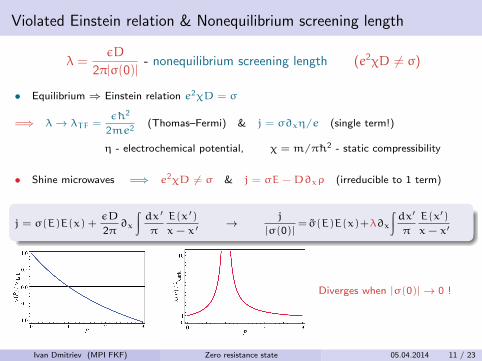
Violated Einstein relation & Nonequilibrium screening length
λ =εD
2π|σ(0)|- nonequilibrium screening length (e2χD 6= σ)
• Equilibrium ⇒ Einstein relation e2χD = σ
=⇒ λ→ λTF =ε h2
2me2(Thomas–Fermi) & j = σ∂xη/e (single term!)
η - electrochemical potential, χ =m/π h2 - static compressibility
• Shine microwaves =⇒ e2χD 6= σ & j = σE−D∂xρ (irreducible to 1 term)
j = σ(E)E(x) +εD
2π∂x
∫dx ′
π
E(x ′)
x− x ′→ j
|σ(0)|=σ(E)E(x)+λ∂x
∫dx′
π
E(x′)
x− x′
Diverges when |σ(0)|→ 0 !
Ivan Dmitriev (MPI FKF) Zero resistance state 05.04.2014 11 / 23

Step 2: Domain solution in unbiased finite system
• Solve j = 0 in 2D stripe of width L → parameter l ≡ L/πλ
2DEG
x
y
z
0
• Plane contacts do not create nonuniform ρ(x)
⇒ Spontaneous symmetry breaking
• Image charges → periodicity: E(x) = E(x+ 2L)
• Boundary conditions: ρ(0) = ρ(L) = 0
l=L/πλ
l = 30
l = 10
l = 2
l = 1.1
l = 1.01
E(x)
Ec= −
2
πarctan
(√l2 − 1 cos
πx
L
) 2πρ(x)
εEc=
2
πartanh
(√1−l−2 sin
πx
L
)
Ivan Dmitriev (MPI FKF) Zero resistance state 05.04.2014 12 / 23

Size-dependent instability threshold: σc = −εD/2L
Fluctuations e−ηqteiqyy sin(qxx) Stability: ηq = 2πεq
(σd(Ex)q
2x +σ(Ex)q
2y
)+Dq2 > 0
Consider linear stability of the uniform ρ ≡ 0 unbiased E ≡ 0 state:
• L→∞: long-wavelength (q→ 0) instability at σc = 0
• Finite L: q > π/L ⇒ instability shifts to σc = −εD/2L ⇔ l ≡ L/πλ = 1
π
23/2EcE(x) = −
√l− 1 cos
πx
Lπ2
21/2εEcρ(x)=
√l− 1 sin
πx
Ll=
L
πλ
l = 30
l = 10
l = 2
l = 1.1
l = 1.01
Ivan Dmitriev (MPI FKF) Zero resistance state 05.04.2014 13 / 23

Step 3: Domain solution in a biased 2D stripe
• Solve sinπE
Ec− λ ∂x
∫dx ′
Ec
E(x ′)
x− x ′= j; (Anti)dissipative current j =
π j
σ(0)Ec
0.0 0.2 0.4 0.6 0.8 1.0
0.0
-0.5
-1.0
0.5
1.0
L / pl = 3
x L/
EE
/c
j = {0, 0.25, 0.5, 0.75, 0.9, 8/9}
0.0 0.2 0.4 0.6 0.8 1.0
0.0
-0.5
-1.0
0.5
1.0
x L/
EE
/c
j = {0, 0.03, 0.1,
0.5, 0.9, 899/900}
L / pl = 30
Finite bias j: Shift w(j) and broadening β(j) of the domain wall
Full solution: Ψ ≡ π
2EcE+ i
π2
εEcρ = i ln
cosh(ξ− iw)
sinhξ−
1
2arcsin j, |j| 6
√1 − l−2,
where 2ξ = iπ(x/L− 1/2) + iw+β, w = arctan(jl), β = arcoth(l
√1 − j2)
Ivan Dmitriev (MPI FKF) Zero resistance state 05.04.2014 14 / 23

Domains ⇒ zero resistance/conductance
Hall bar Corbino
Andreev,Aleiner,Millis’03
Domains with jc⊥Ec = ρHjc,
where σ(Ec)=0 and ρH=B/enc.
External biasmoves the domain wall
Hall bar – zero resistance state:
V=0 for any I= jc(L1 − L2)
Corbino – zero conductance state:
I = 0 for any V = Ec(L1 − L2)
Ivan Dmitriev (MPI FKF) Zero resistance state 05.04.2014 15 / 23

Negative conductance: Linear response
Small V: j =<σ> V/L
Conductance G =<σ> /L
• L < π/λ : <σ>= σ(0)
• L� λ :<σ>
σ(0)=πλ
2L
<s
>
s(0)
01
2L / pl -1
s(0)
e-L / l3D
L / pl
3D electrostatics, ∂xE = 4πρ/ε −→ <σ>
σ(0)∼ e−L/λ3D , λ3D=
√εD
4πσ(0)
Appropriate description for 3D ruby crystals Dyakonov’84, Dyakonov,Furman’84
Also utilized to describe ZRS in 2DA. F. Volkov and V. V. Pavlovskii, Phys. Rev. B 69, 125305 (2004)A. Auerbach et al., Phys. Rev. Lett. 94, 196801 (2005)I. G. Finkler and B. I. Halperin, Phys. Rev. B 79, 085315 (2009)
Ivan Dmitriev (MPI FKF) Zero resistance state 05.04.2014 16 / 23

General approach to stability: Lyapunov functional
Lyapunov functional Φ = K−G: Stable solution ≡ Global minimum of Φ
Application to ZRS (3D, limit λ� L) Auerbach,Finkler,Halperin,Yacoby’05
• Bulk gain G=−
∫dx
E(x)∫0
σ(E ′)E ′dE ′ : σ < 0 ⇒ Maximized for |E(x)|=Ec
• Domain walls K =D
2
∫dxE(x) CE(x)> 0 ⇒ Minimized for ∂xE=0
capacitance C: ρ(x) = Cφ(x)
Sine model: Φ=πλ
8E2c
∫dxdx ′
[E(x) − E(x ′)
x− x ′
]2
−
∫dx sin2 πE
2Ec> −1
Ivan Dmitriev (MPI FKF) Zero resistance state 05.04.2014 17 / 23
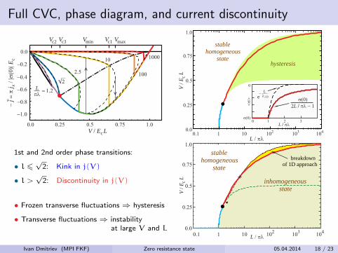
Full CVC, phase diagram, and current discontinuity
2.5
10
100
1000
2
0.0 0.5 1.0
-1.0
-0.8
-0.6
-0.4
-0.2
0.0
V / E Lc
- j
= p j
/ |s(0)|
Ex
c
L = 1.2pl
0.25 0.75
Vc3 Vmin Vc1 VmaxVc2
<s>
s(0)
0
1L / pl
3
0.1 1 10 210 310 410L / pl
stablehomogeneous state
0.25
0.0
1.0
0.5
0.75
V /
EL
c
hysteresis
2L / pl - 1
s(0)
L -l3De
0 2
1st and 2nd order phase transitions:
• l 6√
2: Kink in j(V)
• l >√
2: Discontinuity in j(V)
• Frozen transverse fluctuations ⇒ hysteresis
• Transverse fluctuations ⇒ instabilityat large V and L
0.1 1 102
103
104
10
0.25
0.0
1.0
0.5
0.75
V /
EL
c
L / pl
stablehomogeneous state
in state
homogeneous
breakdown of 1D approach
+
Ivan Dmitriev (MPI FKF) Zero resistance state 05.04.2014 18 / 23

Possible 2D domain structure at low and high bias
• Finkler,Halperin’09: DWs at π/4 to E in domains, ρ∝∂xE (3D)
=⇒ � structure is stable, Φ� ≶ Φ1D, for ∂2Eσ↘ with E
• High bias structure in 1D (L↑ � L) vs 2D (Double domain walls)
• Realistic 2D electrostatics (ρ∝x−1 ◦ E) ⇒ Φ� > Φ1D
=⇒ 1D domain structure is preferable ⇒ different 2D structure at high V
Ivan Dmitriev (MPI FKF) Zero resistance state 05.04.2014 19 / 23
Summary
Analytic model for the domain state in a biased 2D stripe
Step 1: Domain state in unbiased large system, L→∞, V → 0
Step 2: Finite-size effects in unbiased system
Step 3: Domain state in biased finite system
Outcome:
• Nontrivial dependence of domain structure on system size L and bias V
• V − L phase diagram including continuous and discontinuous phase transitions
• Transverse instability at large V and L: transition to a 2D domain state
Ivan Dmitriev (MPI FKF) Zero resistance state 05.04.2014 20 / 23

Direct evidence for static domains in ZRS?
Random telegraphphotovoltage signals betweeninternal probes undercontinuous microwaveillumination
Interpreted as spontaneousswitching between two nearlydegenerate configurations ofdomains
Dorozhkin,Pfeiffer, West, von Klitzing, Smet’11
configuration I configuration II
UB4, B5
UB3, B4
UB2, B3
UB1, B2
Ui, j
Time t (s)-1.0 -1.5 0.0
- 0
- 0
- 0
- 0
- 0
B
1 mV
B BA AC C
SSD D
1
2
34
5
I I
Ivan Dmitriev (MPI FKF) Zero resistance state 05.04.2014 21 / 23
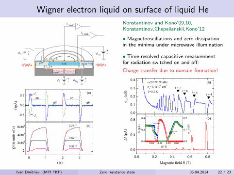
Wigner electron liquid on surface of liquid He
SSE
liquid 3He
sinter
VB VG1
VF VG2
+ +
++-
- -
-
G2 C2 C1
G1 B
F �y�y�y�y�y�y�y�y�y�y�y�y�y�y�y�y
I1
I2
0 1 2 3
I2
t (s)
2x10⁵
4x10⁵
6x10⁵
Q (i
n un
its o
f e)
I1
-0.3
0.0
0.3
(b)
off
on
I (pA
)
0
on
off
0.52 T
0.62 T
0.78 T
(a)
0
Konstantinov and Kono’09,10,Konstantinov,Chepelianskii,Kono’12
• Magnetooscillations and zero dissipationin the minima under microwave illumination
• Time-resolved capacitive measurementfor radiation switched on and off:
Charge transfer due to domain formation!
0.0 0.2 0.4 0.6 0.8
0.0
0.4
0.8 (b)
I (pA
)
Magnetic field B (T)
(a)
0.0
0.1
0.2
0.3
0.4
l = 7l = 6 l = 5
xx (n
S)
/2 =90.9 GHzns=1.4x106 cm-2
T=0.2 Kl = 4
0.60 0.62 0.64 0.660.0
0.1
0.2
xx (n
S)
B (T)
0.0
0.2
0.4
I (pA
)
Ivan Dmitriev (MPI FKF) Zero resistance state 05.04.2014 22 / 23

Importance of transverse fluctuations by example of ruby
• Laser-illuminated Ruby Al2O3 : Cr3+
→ Spontaneous field E ∼ ±106 V/cm
along or against the trigonal axis C3
detected in the luminescence ofStark-shifted Cr3+ levels
No transverse fluctuations are possible!
⇒ Homogeneous state with σd > 0 isstable whatever σ is (σ > 0 or σ < 0)
⇒ Hysteresis with respect to directionof electric field sweep
Experiment: Liao,Glass,Humphrey’80Basun,Kaplyanskii,Feofilov’83,’84
Theory of domains: Dyakonov’84Dyakonov,Furman’84
j · E < 0 is stable!
Ivan Dmitriev (MPI FKF) Zero resistance state 05.04.2014 23 / 23