zeolite surface as a catalyst support material for ...maruyama/papers/11/moteki.pdf · 1 zeolite...
TRANSCRIPT
1
Zeolite Surface as a Catalyst Support Material for
Synthesis of Single-Walled Carbon Nanotubes
Takahiko Moteki,1 Yoichi Murakami,
1,2 Suguru Noda,
1 Shigeo Maruyama,
3 Tatsuya Okubo,
1,*
1 Department of Chemical System Engineering, The University of Tokyo, 7-3-1 Hongo, Bunkyo-ku,
Tokyo 113-8656, Japan
2 Global Edge Institute, Tokyo Institute of Technology, 2-12-1 Ookayama, Meguro-ku, Tokyo 152-8550,
Japan
3 Department of Mechanical Engineering, The University of Tokyo, 7-3-1 Hongo, Bunkyo-ku, Tokyo
113-8656, Japan
RECEIVED DATE (to be automatically inserted after your manuscript is accepted if required
according to the journal that you are submitting your paper to)
* Corresponding author
FAX: +81-3-58003806
E-mail address: [email protected] (T. Okubo)
Preparation of high-quality single-walled carbon nanotubes (SWNTs) has been advanced by controlling
several parameters including the catalyst and the catalyst support material. Although zeolite has been
frequently used as a catalyst support material for the synthesis of SWNTs, detailed surface properties of
previously employed zeolites, and thus their role as a catalyst support material, have not been
2
sufficiently clarified yet. In this study, a clean b-plane surface of silicalite-1, which is a siliceous MFI-
type zeolite, was used as a model substrate for the synthesis of SWNTs. The amount of active cobalt
used for SWNT generation was smaller than the initially sputtered amount, and XPS measurements
revealed diffusion of cobalt into the zeolite framework. The diffused cobalt was found to interact
strongly with the silica framework of zeolite. The diffusion coefficient of cobalt in silicalite-1 zeolite
was estimated to be one order of magnitude larger than that in thermally oxidized SiO2 formed on a Si
substrate. This difference was ascribed to the microporous structure and lower density of zeolite. In this
study, the state of the cobalt catalyst and the interaction between cobalt and the crystalline zeolite
substrate is presented and discussed.
Keywords: silicalite-1; surface; single-walled carbon nanotubes; catalytic chemical vapor deposition;
XPS; diffusion;
1. Introduction
Single-walled carbon nanotubes (SWNTs) have attracted attention because of their unique electric,
mechanical, and chemical properties that are promising for many applications [1]. Mass production of
high-quality SWNTs has been an important objective to support these applications. Thus far, SWNTs
have typically been synthesized by the catalytic chemical vapor deposition (CCVD) method [2]. In this
method, SWNTs are catalytically grown from metal nanoparticles (which are often supported on stable
oxide materials such as silica, alumina, and magnesium monoxide) that are exposed to gas-phase carbon
sources at elevated temperatures. The choice or design of the support material is an important aspect
because it affects the diameter distribution of the catalyst nanoparticles formed, which eventually affects
the diameter distribution of the SWNTs. In this context, the control and elucidation of interactions
between the metal catalyst and the oxide support material has been the central problem in CCVD
synthesis of SWNTs.

3
Zeolite is a class of oxide support materials that has been employed to address the above-mentioned
problem [2c, 2f, 2g, 2h]. Zeolites are a group of microporous crystalline aluminosilicate and nearly 200
distinct frameworks of zeolites are presently known. Each framework has a unique void structure and
pore dimension, and can accommodate a range of Si/Al ratios, which adds variety to the zeolite matrix.
Because of the voids, zeolite has lower density (typically 1.7 g/cm3) compared to other support materials,
such as the dence SiO2 materials (2.20 g/cm3 for amorphous silica glass and 2.65 g/cm
3 for crystalline
quartz) [3].
However, the characteristics of zeolite powders used in previous studies [2c, 2f, 2g, 2h], such as the
dominantly utilized crystallographic plane, the degree of surface flatness, and the degree of adhesion of
amorphous silica, were not described. Furthermore, the influence of the zeolite surface on the supported
metal species was not clearly presented. In some studies [2c, 2g, 2h], the so-called USY zeolite (USY
signifies “ultra-stable Y”) with an FAU-framework was employed because of its high thermal stability.
In general, as the Si/Al ratio in zeolite increases, the thermal stability improves. USY zeolite is a post-
synthetic zeolite with a high Si/Al ratio (>200) fabricated from a Y-type zeolite (Si/Al > 1.5). However,
the grains of USY zeolite are known to be mesoscopically rough, sometimes accompanying open
mesopores that extend into the grain as a result of strong acidic post chemical treatments used to extract
Al from Y-type zeolite [4]. Typical transmission electron microscope (TEM) images of USY zeolite
measured by us are shown in Supporting Information 1. Thus, from the above-mentioned data, the
intrinsic influence of zeolite surfaces on the catalyst species for SWNT growth was ambiguous. This
was partly due to the fact that the zeolites in these studies were purchased from a supplier and generally
used without further characterization, a consequence of the challenges associated with the synthesis of
high-quality zeolite with fine crystalline surfaces.
In this study, we have investigated the surface properties of a zeolite used as a catalyst support
material for SWNT synthesis for the first time by employing a specific crystallographic plane of a
zeolite with characterized quality. In particular, we studied an atomically flat b-plane of silicalite-1
zeolite (density: 1.81 g/cm3, MFI-framework, see Supporting Information 2 for structural details) [5].
4
We have chosen silicalite-1 because its Si/Al ratio is virtually infinite, and hence, high thermal stability
is expected. We demonstrate that the diffusion of the metal catalyst deposited on the zeolite surface to
the inside of the zeolite is an important factor that affects the catalytic growth of SWNTs, which had not
been considered previously. Such diffused metal species are found to be incorporated into or strongly
interacting with the silica framework of zeolites. The observed diffusion is explained in terms of the
microporous structure and lower density of zeolite, which is distinctly different from the cases of dense
silica support materials.
2. Experimental Section
2.1. Sample preparation
2.1.1. Zeolite synthesis
Silicalite-1 crystals with a clean b-plane (see Supporting Information 2 for the crystal geometry) were
synthesized according to a previously reported procedure [6]. Typically, 3.125 g of
tetrapropylammonium bromide (TPA-Br, Aldrich), which works as an organic structure-directing agent
(SDA), and 0.466 g of sodium hydroxide (Wako) were added to 200 g of distilled water. Subsequently,
23.164 g of tetraethoxysilane (TCI) was added to the solution. The phase-separated liquid mixture was
stirred at room temperature for 48 h until the mixture had reacted completely to become a clear
homogeneous solution. The molar composition of the mixture was 0.1 TPA-Br: 1 SiO2: 0.05 Na2O: 98
H2O. After homogenization, the solution was aged at 323 K for 7 days with stirring. It was then filtered
and sealed in a 50-mL homemade stainless steel autoclave and rotated at 20 rpm for 2 days at 403 K.
The solid product was filtered, washed with distilled water, and finally dried at 333 K for 24 h.
2.1.2. Substrate preparation
A b-oriented silicalite-1 crystal monolayer was prepared according to the reported method [7]. As-
synthesized silicalite-1 crystals were evacuated in a flask at 453 K to remove adsorbed water. After the
flask was cooled down to room temperature under an inert gas, an excess of 2-butanol was added. The
resulting mixture was refluxed for 48 h to functionalize the crystal surface with 2-butanol by
5
dehydration condensation. The functionalized crystals were then dispersed into a 2-butanol solvent. A Si
substrate deposited with an 80-nm-thick Ti layer was first covered with a thin layer of water, and then
the zeolite suspension was gently placed on the water layer. Slow evaporation of 2-butanol and then
water (both took place at room temperature) resulted in the formation of a monolayer of the zeolite
crystals on the substrate surface. The substrate was calcined in an electronic furnace under air at 823 K
for 5 h to remove the occluded organic SDAs and 2-butanol from zeolite. A Si substrate with a 50-nm
thermally oxidized silica layer (TO-SiO2) was used as the control sample.
2.1.3. Catalyst deposition
Cobalt catalysts used for SWNT growth were deposited on the substrates by a spatial gradient
sputtering method with a slit mask [8]. Since the deposition rate varies exponentially according to the
lateral distance from the slit position, a large variation in the thickness of the cobalt deposits was
established on the substrate. As shown by Figure S3 in the Supporting Information, the calculated
average thickness varied from 0.64 nm to 0.02 nm. As for the samples used to investigate the chemical
state of cobalt by X-ray photoelectron spectroscopy (XPS), cobalt was uniformly deposited on the
substrates (average thickness: 0.1 nm) without using the slit mask.
2.1.4. SWNT synthesis
SWNTs were synthesized by alcohol CCVD [2g] using a procedure described in Ref. 2h. Briefly, the
substrates were placed in a quartz tube held inside an annular electric furnace. After evacuation, the
furnace was heated to 1073 K and the contents of the tube were exposed to a flowing gas mixture of
Ar/H2 (3% H2, 300 sccm) at 40 kPa to reduce oxidized cobalt. After the furnace reached 1073 K, a
holding time of either 1 or 10 min, the “pre-reduction time,” was imposed before initiating the
introduction of ethanol vapor (carbon source) into the quartz tube. Ethanol vapor (450 sccm) was then
passed through the quartz tube at 0.31 kPa for 30 s without a carrier gas. SWNTs were only grown on
the top surfaces (or b-surfaces, as shown below) of zeolite crystals because cobalt deposited on the
surface of the Ti-coated substrate was deactivated by the Ti layer at 1073 K.
2.2. Sample characterization
6
The structures of the obtained zeolite were examined with a powder X-ray diffractometer (XRD)
(M03X-HF, Bulker AXS) using Cu Kα radiation at a scanning rate of 4 deg/min over a range of 5–45
degree (2 theta). The microscopic surface morphology of the zeolite crystals was characterized with an
atomic force microscope (AFM) (SPI-3800N, SII). The morphologies of the zeolite and the synthesized
SWNTs were measured by a field emission scanning electron microscope (FE-SEM) (S-4800, Hitachi)
at a low accelerating voltage of 1 kV. SWNTs were also characterized by a microscope Raman
scattering spectroscopy system (excitation wavelength: 488 nm) and a microscope photoluminescence
(-PL) spectroscopy system. The chemical states of the zeolite and the cobalt catalyst were characterized
by XPS (PHI Quantera SXM, Physical Electronics).
3. Results
3.1. Characterizations of synthesized zeolite crystals
Figure 1 shows XRD patterns measured from the zeolite samples. All peaks from the as-synthesized
crystals (Fig. 1(a)) are explained in terms of the MFI-framework structure. The structure was maintained
even after the crystals underwent the CVD process (Fig. 1(b)). After those crystals were mounted on the
Ti-coated Si substrate, peaks corresponding to the (h00) and (0k0) planes became dominant (Fig. 1(c)),
indicating that most of the silicalite-1 crystals were mounted aligning with either the a-plane or the b-
plane parallel to the substrate.
Figure 2 shows a top-view SEM image of the sample corresponding to Fig. 1(c). The obtained
silicalite-1 crystals have a coffin-like shape with dimensions of approximately 10 × 7 × 2 m. The b-
plane tends to be the largest surface plane in the silicalite-1 crystals synthesized with TPA [9]. The
detailed geometry is shown in Supporting Information 2. Most of the crystals were mono-dispersed on
the substrate with their b-planes aligned parallel to the substrate, while aggregates of a few crystals were
occasionally seen.
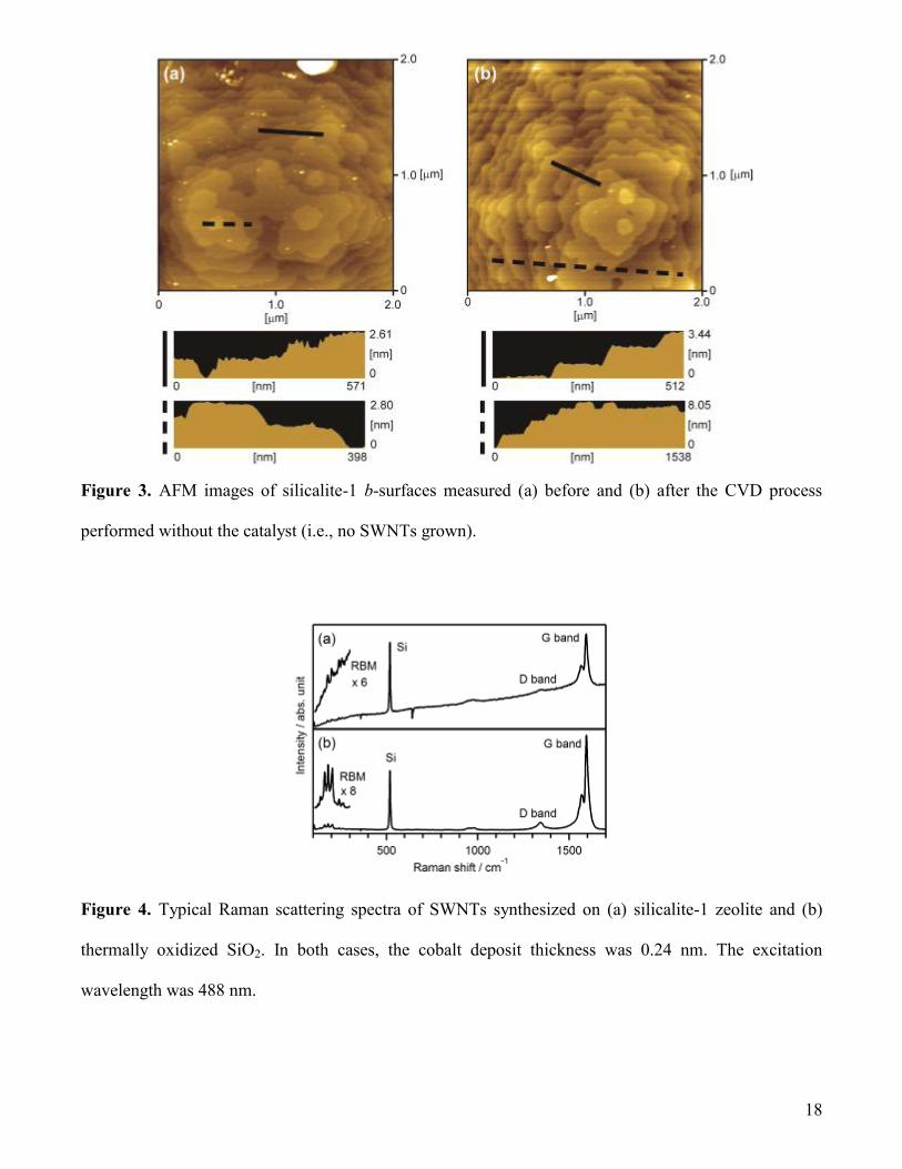
Figure 3(a) shows the morphological image of the b-plane measured by AFM, while Figure 3(b)
shows the image of the same sample after it underwent the CVD process in the absence of the cobalt
7
catalyst (i.e., no SWNTs grown, corresponding to Fig. 1(b)). Both these images show flat surfaces with
steps of distinct height (ca. 1.0 nm). The ratio of lateral inter-step distance to step height is about 100 or
higher. As can be seen, the surfaces were crystallographically clean and free from amorphous silica
deposits, and the surface morphology essentially did not change during the CVD process. As stated
previously, the thermal stability of zeolite increases with increase in the Si/Al ratio. The thermal stability
of silicalite-1, which does not contain Al (Si/Al ≈ ∞), is hence much higher than that of other common
aluminosilicate zeolites that typically have the ratio on the order of unity. The concentric step patterns
seen in the AFM images were formed as a result of crystal growth [6]. The same concentric patterns
have also been observed with FE-SEM at 1 kV accelerating voltage (data not shown). The observed
height of the steps (ca. 1 nm) agrees with the structural periodicity along the b-axis of the MFI
framework structure (0.99 nm, see Supporting Information 2).
3.2. Dependence of the amount of synthesized SWNTs on the quantity of supported catalyst
Figure 4 shows typical Raman scattering spectra from SWNTs synthesized on the b-surface of
silicalite-1 or TO-SiO2. A detailed interpretation of Raman spectra of SWNTs has been presented
elsewhere [10]. Briefly, a prominent peak at 1593 cm−1
and a weaker peak at around 1350 cm−1
are G-
band (G for graphite) and D-band (D for defect) peaks, respectively. The high G-band to D-band ratio in
Fig. 4 implies that the SWNTs are of high quality. In addition, several peaks are observed in the 150–
300 cm−1
region, which are for “radial breathing mode (RBM)” corresponding to the axial-symmetric
radial vibration. Observation of RBM peaks indicates SWNTs [10] and this feature is usually not
observed with multi-walled carbon nanotubes. The sharp peak at 520 cm−1
is associated with the Si
substrate. As shown in Fig. 4(a), the Raman scattering spectrum from the silicalite-1 sample shows a
strong background that increases monotonically with Raman shift, which is attributed to zeolite
luminescence. The peak position of RBM features depends on the diameter of SWNTs [10]. However,
the spectral shape of the RBM range merely provides a rather rough estimation of the diameter
distribution of SWNTs. There are two reasons for this: (i) Raman scattering from SWNTs is a resonant
scattering process, and hence, RBM shape significantly varies with the excitation wavelength [10, 11].

8
(ii) The intensity of RBM peaks strongly depends on not only the SWNT diameter but also the wall
helicity (or “chiral angle”) of SWNTs [12].
Figure 5 shows the dependence of the G-band intensity on the deposit thickness of the cobalt catalyst
(Figs. 5(a) and 5(b)) and the corresponding SEM images (Figs. 5(c) and 5(d), respectively). As shown by
the upper labels depicted along the x axis of Figs. 5(a) and 5(b), the average thickness of deposited
cobalt was spatially varied from 0.64 nm to 0.02 nm by the gradient sputtering method, as mentioned
above. The plotted marks in those figures represent averaged values of the G-band intensities from 10
measurements at the same lateral distance from the mask’s slit position. Each vertical bar attached to a
mark represents the data scattering range (1) and is not an error bar for the measurement. Therefore, we
assume that the averaged values are reliable. On the silicalite-1 crystal, the average cobalt thickness
giving the maximum G-band intensity was in the range 0.15–0.24 nm (triangles in Fig. 5(a)) and did not
show a noticeable shift on increasing the pre-reduction time (circles in Fig. 5(a)). The corresponding
SEM images (Fig. 5(c)) show that randomly oriented SWNT bundles were abundantly grown in this
range. In the case of the TO-SiO2 substrate (control sample) [13, 14], the average value of the G-band
intensity was maximized in the average thickness range 0.15–0.24 nm (triangles in Fig. 5(b)). By
increasing the pre-reduction duration at 1073 K from 1 min to 10 min, the average thickness giving the
maximum G-band intensity shifted slightly toward the 0.10–0.15 nm range (circles in Fig. 5(b)).
3.3. Behavior of the cobalt catalyst deposited on silicalite-1 and TO-SiO2
Table 1 compares the atomic ratios of cobalt on silicalite-1 sample to those on the TO-SiO2 sample
measured by XPS for different pre-reduction times. It is observed that the cobalt atomic ratio on the
silicalite-1 surface decreases remarkably with increase in the pre-reduction time. In contrast, the ratio on
the TO-SiO2 substrate increases slightly by the same treatment.
To investigate the distribution of cobalt inside the samples, we performed Ar-ion etching of the
samples. In this experiment, the atomic ratio of cobalt was repeatedly measured by XPS after each
etching step (performed for 12 s, at an applied voltage of 4 kV). Figure 6 shows the depth profiles of the
cobalt atomic ratio for the silicalite-1 and TO-SiO2 samples. The horizontal axis denotes the number of

9
etching cycles. On the b-plane of the silicalite-1 crystal, cobalt atoms are localized near the crystal
surface before the reductive thermal treatment (open circles in Fig. 6). However, after the 1-min
reductive thermal treatment, the atomic ratio at the surface significantly decreased and the ratio inside
the crystal increased to ~ 0.3% for the depth corresponding to many etching cycles (solid circles in Fig.
6). This suggests that cobalt diffused deep into the crystal. In the case of the TO-SiO2 substrate, cobalt
remains localized near the surface after the same treatment (crosses in Fig. 6). The depth etched by one
etching step in the case of the silicalite-1 crystal has been estimated to be 4 nm based on the measured
etching rate of 20 nm/min from a cross-sectional SEM observation of the sample. On the other hand, the
depth etched out by one etching step in the case of the TO-SiO2 substrate has been estimated to be 3.1
nm based on the etching rate of 15.6 nm/min for a reference SiO2 substrate. The higher etching rate
observed for zeolite is attributed to its lower density compared with that of thermally oxidized SiO2.
Figure 7 shows the binding energy (BE) of Co 2p levels for “as-sputtered” and “1-min reduced” cobalt
catalysts deposited on the silicalite-1 crystal (Fig. 7(a)) and on the TO-SiO2 substrate (Fig. 7(b)). The
spectra were calibrated with a peak of C 1s level from adventitious carbon at 284.6 eV corresponding to
the C–C bond [15]. The peaks in Fig. 7 were separated into a main peak of Co2+
at 781.2–781.9 eV and
its shake-up satellite at 785.2–785.7 eV. Although the observed BE for the main peak coincides with
that for a silicide-like compound (at 781.3–781.9 eV [16]), the absence of this peak as well as the
absence of carbide has been confirmed by the spectra of Si 2p and C 1s levels (Supporting Information
4). The main peak positions measured from silicalite-1 are noticeably different from those of TO-SiO2.
The main peaks from silicalite-1 corresponding to Co2+
(781.7–781.9 eV) were observed at higher
positions (by ca. 0.5 eV) than those from TO-SiO2 (781.2–781.4 eV). In the case of TO-SiO2, the BE is
assigned to Co2+
in CoO. This assignment is justified because the thickness of deposited cobalt was so
small that the as-sputtered catalyst was believed to have been promptly oxidized by exposure to air. A
previous study [17] reported that when the amount of CoO is small, this peak is observed at higher
energy than the peak for Co2+
in bulk CoO, which is observed at 780.0–780.7 eV. On the other hand, in
the case of silicalite-1, we attribute the shift to a higher BE of Co2+
interacting with the silica
10
frameworks of the zeolite. Previous publications have reported that the BEs observed at 781.7–782.5 eV
is an indication of strong interactions between Co2+
ions and the silica frameworks [18] or the
incorporation of Co2+
ions into the silica frameworks [18a].
4. Discussion
The amount of SWNTs produced can be estimated from the intensity of the G-band as a first
approximation. Therefore, in Fig. 5, the cobalt nanoparticles formed in the region where the G-band
intensity was maximized were believed to have had optimal sizes to catalyze the growth of SWNTs. In
the case of the TO-SiO2 substrate, the shift in the optimal cobalt deposit thickness toward a smaller
value was observed by prolonging the pre-reduction time (Fig. 5(b)). This shift can be explained in
terms of an increase in the diameter of the cobalt nanoparticles resulting from thermal agglomeration or
Ostwald ripening, as observed previously [8, 14, 19]. The number-counting histograms of the emission
wavelengths measured by -PL spectroscopy from individual SWNTs grown on the silicalte-1 sample
are shown in Figures S5 and S6 in the Supporting Information; this data confirms that the ratio of small
diameter SWNTs becomes larger as the thickness of deposited cobalt becomes smaller.
In the case of the silicalite-1 sample, an increase of the pre-reduction time did not change the optimal
thickness (Fig. 5(a)), in contrast to the case of the TO-SiO2 substrate (Fig. 5(b)). This implies that a
discussion focusing only on catalyst agglomeration or Ostwald ripening, which often accounts for the
observed behavior of metal catalysts on non-porous flat oxide substrates, does not sufficiently explain
the behavior observed for silicalite-1 zeolite. Some previous studies that employed zeolite as a catalyst
support material for SWNT growth anticipated that the microporous structure of zeolite might serve as a
template for metal nanoparticles or as physical resistance against thermal agglomeration [20]. While
such a role of the zeolite surface is not excluded, on the basis of our experimental results (Figs. 5 and 6),
we propose that the diffusion of deposited metallic species into zeolite crystals is the primary effect to
be considered when zeolite is employed as a support material. Furthermore, no SWNTs were
synthesized when the cobalt deposit thickness was less than 0.07 nm on the silicalite-1 crystal (Fig. 5(a)),
11
which is distinctly different from the case of TO-SiO2 (Fig. 5(b)). These results suggest that the
diffusion of metallic species supported on the surface to the inside of zeolite is an important process
competing with thermal agglomeration on the surface [18b]. The result shown in Fig. 5(a) implies that
the former is more significant than the latter in the present study.
The result shown in Fig. 6 provides a clue for estimating the elemental diffusivity of cobalt inside a
silicalite-1 crystal. To investigate this point, we begin by considering the case of TO-SiO2 where the
diffusion distance of cobalt was limited to the depth corresponding to one etching step (≈ 3.1 nm, Fig. 6).
The diffusion distance, [cm], is defined in terms of the diffusion coefficient D0 [cm2 s
−1], the
activation energy [eV], and the temperature T [K] as shown in equation (1).
Dt , kTeDD 0 (1)
where k denotes the Boltzmann constant. Using the bulk diffusion constant of cobalt in SiO2 (electronic
grade) (D0 ≈ 1.0 × 10⁻⁷
cm2 s
−1 and = 1.7 eV [21]), the diffusion distance is calculated to be 2.49 nm.
This is close to the diffusion distance we estimated above on the basis of our etching experiment (≈ 3.1
nm). On the other hand, from the same experiment, the cobalt diffusion in silicalite-1 has been found to
span roughly 3–4 etching cycles (Fig. 6). Since the etching rate for silicalite-1 has been estimated to be
≈ 4 nm/step (Section 3.3), the diffusion distance is roughly calculated to be 12–16 nm, or more broadly
10–20 nm. Although the diffusion of cobalt should also have occurred during the time required to
increase the temperature to 1073 K, we can assume that the results for TO-SiO2 and for silicalite-1 in
Fig. 6 are comparable because both samples underwent an identical thermal process. Because D 2
(Eq. (1)), the diffusion constant (D0) of cobalt in silicalite-1 can be estimated to be 10–40 times (i.e.,
one order of magnitude) higher than that in TO-SiO2. In other words, the order-of-magnitude estimated
diffusion constant of cobalt in silicalite-1 crystals is D0 ~ 1 × 10⁻⁶
cm2 s
−1.
The observed diffusion of cobalt correlates with the XPS data shown in Fig. 7. As described in
Section 3, the existence of a strong interaction between Co2+
and the silica framework has been implied
by XPS data. Furthermore, the intensity ratio of the shake-up satellite of Co2+
(at 785.5–785.7 eV) to the
12
primer Co2+
(at 781.7–781.9 eV) in the case of silicalite-1 became larger after the reductive thermal
treatment (Fig. 7(a)). This strong shake-up satellite suggests that most of the diffused cobalt is in the
form of isolated Co2+
ions [22]. This suggestion is supported by the previous observation that
framework defect sites (Si–OH or Si–O−) strongly capture Co2+
ions and that certain types of cage-like
structures also stabilize the Co2+
ions [18a]. Thus, this interaction is considered to be sufficiently strong
to the extent that the complete reduction of Co2+
incorporated in zeolite is hardly possible. Therefore, we
consider the signal near 781.7–781.9 eV in Fig. 7(b) to be a superposition of two different Co2+
species:
one originating from Co2+
ions that are incorporated in the silica framework, and the other originating
from Co2+
in CoO that is to be reduced during the CVD process to generate the metallic cobalt species
that eventually catalyzes SWNT growth.
On the basis of the discussion above, the behavior of a metal catalyst supported on a zeolite is
summarized as follows: A part of the metal species deposited on the zeolite surface is diffused into the
zeolite as a result of a high-temperature reductive environment during the CVD process. We believe that
the diffusion can be ascribed to the low density and microporous structure of zeolite, which is distinctly
different from other more dense silica materials such as TO-SiO2. The metal catalyst diffused into the
zeolite is considered to be incorporated into the silica framework, and hence becomes inactive as a
catalyst for SWNT growth. As a result, a greater amount of cobalt deposited on the zeolite surface is
necessary to generate active catalytic particles, suggested by the comparison between Figs. 5(a) and 5(b).
From a different viewpoint, catalyst agglomeration or Ostwald ripening that leads to an increase in
SWNT diameters [23], which has been a problem in using the conventional non-porous substrates for
SWNT growth [19], is less significant and mitigated on the surface of zeolite crystals.
5. Conclusions
The behavior of cobalt deposited on the clean b-plane of silicalite-1 zeolite under CVD conditions for
SWNT growth has been clarified for the first time. We compared the role of an atomically flat zeolite
surface with that of non-porous thermally oxidized SiO2 substrates. The cobalt deposited on silicalite-1

13
zeolite has been found to diffuse into the zeolite crystal and is considered to be incorporated into the
framework of the zeolite on the basis of the results of XPS, under a high temperature reductive
environment during the CVD process.
On the silicalite-1 crystals, the amount of cobalt used for SWNT generation is smaller than the
initially sputtered amount. The diffusion coefficient for cobalt in silicalite-1 zeolite has been estimated
to be one order of magnitude larger than that in thermally oxidized SiO2. This higher diffusion rate can
be ascribed to the microporous geometry and low density of zeolite. Thus, we concluded that the
diffusion of deposited metallic species to internal zeolite sites during the CVD process is an important
process competing with thermal agglomeration that could occur on the surface.
ACKNOWLEDGMENT This work was supported by the Research Fellowships of the Japan Society
for the Promotion of Science for Young Scientists. Part of this work was financially supported by a
Grant-in-Aid for Scientific Research (19054003 and 22226006), and Global COE Program “Global
Center for Excellence for Mechanical Systems Innovation.” T.M. is a JSPS research fellow and is
grateful to JSPS for Research Fellowships for Young Scientists. The authors thank Dr. M. Kamiko and
Mr. R. Kimura for XPS measurements.
Supporting Information Available: TEM images, Schematic descriptions, cobalt deposit thickness
profile, XPS spectra, atomic ratios, and number-counting histograms. This material is available free of
charge via the Internet at http://pubs.acs.org.
REFERENCES
1. Dresselhaus, M. S.; Dresselhaus, G.; Avouris, P. In Carbon Nanotubes, Springer: Berlin 2001.
14
2. a) Dai, H.; Rinzler, A. G.; Nikolaev, P.; Thess, A.; Colbert, D. T.; Smalley, R. E. Chem. Phys.
Lett. 1996, 260, 471-475. b) Hafner, J. H.; Bronikowski, M. J.; Azamian, B. R.; Nikolaev, P.; Rinzler,
A. G.; Colbert, D. T.; Smith, K. A.; Smalley, R. E. Chem. Phys. Lett. 1998, 296, 195-202. c)
Mukhopadhyay, K.; Koshio, A.; Sugai, T.; Tanaka, N.; Shinohara, H.; Konya, Z.; Nagy, J. B. Chem.
Phys. Lett. 1999, 303, 117-124. d) Kitiyanan, B.; Alvarez, W. E.; Harwell, J. H.; Resasco, D. E. Chem.
Phys. Lett. 2000, 317, 497-503. e) Flahaut, E.; Peigney, A.; Laurent, C.; Rousset, A. J. Mater. Chem.
2000, 10, 249-252. f) Okamoto, A.; Kawakubo, T.; Hiraoka, T.; Okazaki, T.; Sugai, T.; Shinohara, H.
Mol. Cryst. Liq. Cryst. 2002, 387, 93-98. g) Maruyama, S.; Kojima, R.; Miyauchi, Y.; Chiashi, S.;
Kohno, M. Chem. Phys. Lett. 2002, 360, 229-234. h) Murakami, Y.; Miyauchi, Y.; Chiashi, S.;
Maruyama, S. Chem. Phys. Lett. 2003, 374, 53-58. i) Lim, S.; Ciuparu, D.; Pak, C.; Dobek, F.; Chen,
Y.; Harding, D.; Pfefferle, L.; Haller, G. J. Phys. Chem. B 2003, 107, 11048-11056.
3. Marler, B. Phys. Chem. Minerals 1988, 16, 286-290.
4. a) Horikoshi, H.; Kasahara, S.; Fukushima, T.; Itabashi, K.; Okada, T.; Terasaki, O.; Watanabe,
D. J. Chem. Soc. Jpn. 1989, 3, 398-404 b) Sasaki, Y.; Suzuki, T.; Takamura, Y.; Saji, A.; Saka, H. J.
Catal. 1998, 178, 94-100.
5. Structure Commission of the International Zeolite Association (http://www.iza-
structure.org/databases/)
6. Agger, J. R.; Hanif, N.; Cundy, C. S.; Wade, A. P.; Dennison, S.; Rawlinson, P. A.; Anderson,
M. W. J. Am. Chem. Soc. 2003, 125, 830-839.
7. a) Liu, Y.; Li, Y.; Yang, W. Chem. Commun. 2009, 1520-1522. b) Cheng, C.; Bae, T.; McCool,
B. A.; Chance, R. R.; Nair, S.; Jones, C. W.; J. Phys. Chem. C 2008, 112, 3543-3551.
8. Noda, S.; Sugime, H.; Osawa, T.; Tsuji, Y.; Chiashi, S.; Murakami, Y.; Maruyama, S. Carbon
2006, 44, 1414-1419.
15
9. Bonilla, G.; Díaz, I.; Tsapatsis, M.; Jeong, H.-K.; Lee, Y.; Vlachos, D. G. Chem. Mater. 2004,
16, 5697-5705.
10. Jorio, A.; Pimenta, M. A.; Souza, A. G.; Saito, R.; Dresselhaus, G.; Dresselhaus, M. S. New J.
Phys. 2003, 5, 139.1-139.17.
11. Fantini, C.; Jorio, A.; Souza, M.; Strano M. S.; Dresselhaus, M. S.; Pimenta, M. A. Phys. Rev.
Lett. 2004, 93, 147406.
12. Jiang, J.; Saito, R.; Sato, K.; Park, J. S.; Samsonidze, Ge. G.; Jorio, A.; Dresselhaus, G.;
Dresselhaus, M. S.; Phys. Rev. B 2007, 75, 035405.
13. Noda, S.; Tsuji, Y.; Murakami, Y.; Maruyama, S. Appl. Phys. Lett. 2005, 86, 173106.
14. Kakehi, K.; Noda, S.; Maruyama, S.; Yamaguchi, Y.; Jpn. J. Appl. Phys. 2008, 47, 1961-1965.
15. Moulder, J. F.; Stickle, W. E.; Sobol, P. E.; Bomben, K. D. In Handbook of X-ray Photoelectron
Spectroscopy; Perkin-Elmer Corp.: Eden Prairie, MN 1992.
16. a) Okamoto, Y.; Nagata, K.; Adachi, T.; Imanaka, T.; Inamura, K.; Takyu, T.; J. Phys. Chem.
1991, 95, 310-319. b) Backman, L. B.; Rautiainen, A.; Lindblad, M.; Jylha, O.; Krause, A. O. I. Appl.
Catal. A 2001, 208, 223-234.
17. Hu, M.; Murakami, Y.; Ogura, M.; Maruyama, S.; Okubo, T. J. Catal. 2004, 225, 230-239.
18. a) Guczi, L.; Bazin, D. Appl. Catal. A 1999, 188. 163-174. b) Tang, Q.; Zhang, Q.; Wu, H.;
Wang, Y. J. Catal. 2005, 230, 384-397. c) Robles-Dutenhefner, P.A.; de Silva Rocha, K. A.; Sousa, E.
M. B.; Gusevskaya, E. V. J. Catal. 2009, 265, 72-79.
19. a) Amama, P. B.; Pint, C. L.; McJilton, L.; Kim, S. M.; Stach, E. A.; Murray, P. T.; Hauge, R.
H.; Maruyama, B. Nano Lett. 2009, 9, 44-49. b) Amama, P. B.; Pint, C. L.; Kim, S. M.; McJilton, L.;
Eyinkt, K. G.; Stach, E. A.; Hauge, R. H.; Maruyama, B. ACS Nano 2010, 4, 895-904.
16
20. Hayashi, T.; Kim, Y. A.; Matoba, T.; Ezaka, M.; Nishimura, K.; Tsukada, T.; Endo, M.;
Dresselhaus, M. S. Nano Lett. 2003, 3, 887-889.
21. Fedorovich, N. A. Sov. Phys. Solid State 1980, 22, 1093-1094.
22. a) Bhoware, S. S.; Singh, A. P. J. Mol. Catal. A 2007, 266, 118-130. b) Fierro, G.; Eberrhardt,
M. A.; Houlla, M.; Herculles, D. M.; Hall, W. K. J. Phys. Chem. 1996, 100, 8468-8477. c) Coulter, E.
E.; Sault, A. G. J. Catal. 1995, 154, 56-64.
23 a) Hasegawa, K.; Noda, S. Appl. Phys. Express 2010, 3, 045103-1-3. b) Hasegawa, K.; Noda, S.
ACS Nano 2011, 5, 975-984.

17
FIGURE CAPTIONS
Figure 1. XRD patterns measured from (a) as-synthesized silicalite-1, (b) silicalite-1 that underwent the
CVD process without the catalyst (i.e., no SWNTs grown), and (c) b-oriented silicalite-1 mounted on a
Ti-deposited Si/SiO2 substrate.
Figure 2. SEM image of silicalite-1 crystals mounted on a Ti-deposited Si/SiO2 substrate (top panel),
and schematic of coffin-shaped silicalite-1 crystal (MFI-framework) with the name of each plane
(bottom).
18
Figure 3. AFM images of silicalite-1 b-surfaces measured (a) before and (b) after the CVD process
performed without the catalyst (i.e., no SWNTs grown).
Figure 4. Typical Raman scattering spectra of SWNTs synthesized on (a) silicalite-1 zeolite and (b)
thermally oxidized SiO2. In both cases, the cobalt deposit thickness was 0.24 nm. The excitation
wavelength was 488 nm.

19
Figure 5. (a) and (b): Dependence of the G-band intensities on the lateral distance from the sputtering
mask's slit position (or on the cobalt thickness as indicated by the upper labels along the x axis) for the
silicalite-1 sample and the thermally oxidized SiO2 sample, respectively (triangle: 1-min pre-reduction,
circle: 10-min pre-reduction). (c) and (d): Corresponding SEM images for 1-min pre-reduction samples
at the positions indicated by the arrows shown in panels (a) and (b).
20
Figure 6. Depth profiles of the cobalt atomic ratio for silicalite-1 before reduction (open circle),
silicalite-1 after 1-min reduction (solid circle), and thermally oxidized SiO2 after 1-min reduction (cross).
In all cases, the cobalt deposit thickness was 0.1 nm. Curves are fitted to the plots by the one-
dimensional diffusion equation.
Figure 7. XPS spectrum of Co 2p levels for “as-sputtered” and “1 min reduced” cobalt catalysts,
deposited on (a) the silicalite-1 b-surface and (b) the thermally oxidized SiO2 substrate.

21
Table 1. Atomic ratios of cobalt (sputtered thickness: 0.10 nm) measured on the surface of silicalite-1
and TO-SiO2 substrates for as-sputtered, 1-min pre-reduction, and 10-min pre-reduction cases.
Sample Reduction Co atomic ratio (%)
Silicalite-1
As-sputtered 3.0
1 min. 1.2
10 min. 0.5
TO-SiO2
As-sputtered 3.1
1 min. 4.2
10 min. 4.4