y la-ur- conf-~~io~o -- oct 0 5 ostl
TRANSCRIPT

.c STRAIN HARDENING OF FCC METAL SURFACES INDUCED BY MICROPLOUGHING
Y
R.D. DAY*, R. M. DICKERSON", P.E. RUSSELL** *Los Alamos National Laboratory, Los Alamos, NM 87545 **North Carolina State University, Raleigh, NC 27606
LA-UR- OCT 0 5
ABSTRACT C O N F - ~ ~ I O ~ O -- O S T l Microploughing experiments were used as a method for better understanding the ploughing
mechanism in gold and iridium single crystals. The plough depths ranged from 20 nm in iridium to 1600 nm in gold. Yield stress profiles and "EM analyses indicate that both materials strain harden even when very small volumes of material are involved. Strain hardening theory, as applied to bulk material, is useful in analyzing the results.
INTRODUCTION
Nanotribological mechanisms play an important role in many precision material removal processes. It has been shown that for grinding and polishing [ 11, precision machining [2], and ultraprecision machining [3] that the actual and effective depths of cut that produce the final surface are often less than 1 pm. For such shallow depths of cut, the ploughing mechanism dominates the energy partition. The demand for components with higher degrees of dimensional precision is continually increasing. This consideration prompted a series of microploughing experiments to acquire an understanding of the ploughing mechanism and its effect on the surface of the part being produced.
Single crystals of noble metals (to eliminate effects of surface oxides), of known orientation, and of the same crystallographic structure were chosen for controlled ploughing tests. The two metals chosen were gold and iridium which have face centered cubic structures. In addition to satisfying the above criteria, these metals represent the extremes in mechanical strength properties. The insight gained from these specific and well controlled experiments will provide insight into the basic ploughing process.
EXPERIMENT
Since the depths of cut for these experiments were very shallow, the surface had to be crystalline and as smooth as possible. This proved to be a challenge for the sample preparation. To make the gold samples as smooth as possible, a controlled polishing technique was used with a 1 pm diamond fmal abrasive. The mechanical polish introduced severe mechanical damage' into the surface, This damage was removed by electropolishing for 3 minutes [4] and finally dip etching in boiling aqua regea [5] for 2 minutes. Alpha particle backscattering was used to verify that the prepared surfaces were indeed crystalline.
electropolished for 4 hours in a 2N potassium cyanide solution with a potential of 12 volts (peak- to-peak) at 60 Hz with a stainless steel electrode. The samples were then annealed at 1650" C in a vacuum for 1 hour. Alpha particle channeling was again used to verify that the samples were crystalline at the surface. The Laue back reflection method was used to determine the orientation of the crystals.
The indentor consisted of a single crystal diamond STM tip. The macro geometry of the tip was a three sided pyramid with faces that made a 70" angle with respect to the horizontal. This indentor was mounted to a stand-alone STM head that was connected to a Digital Instruments Nanoscope IIIa controller. The indentor was oriented so one of the pyramid's edges would be parallel to the direction of travel when generating the microplough.
normal to the surface could be measured as the microplough was generated. The resolution of the balance was 0.1 pN; however the uncertainty in the force measurement was +_ 1 pN. The STM head was decoupled from the balance pan by placement on a plate made out of super invar. The
A similar controlled polish was also used for the iridium. The samples were then
The sample was mounted to the balance pan of a Mettler AE 163 electronic balance so the force
L

DISCLAIMER
This report was prepared as an account of work sponsored by an agency of the United States Government. Neither the United States Government nor any agency thereof, nor any of their employees, makes any warranty, express or implied, or assumes any legal liability or responsibility for the accuracy, completeness, or use- fulness of any information, apparatus, product, or process disclosed, or represents that its use would not infringe privately owned rights. Reference herein to any spe- cific commercial product, process, or service by trade name, trademark, manufac- turer, or otherwise does not necessarily constitute or imply its endorsement, rccom- mendation. or favoring by the United States Government or any agency thereof. The views and opinions of authors expressed herein do not necessarily state or reflect thasc of the United States Government or any agency thereof.

DISCLAIMER
Portions of this document may be illegible in electronic image products. Images are produced from the best available original document.

I plate had a hole in it allowing the sample to be imaged by the STM. This experimental configuration is shown in figure 1.
1 ’ Mettler
Balance 3 Head
Figure 1 - Schematic of microploughing experimental arrangement. The sample rests on the balance pan of the Mettler electronic balance which is shown by a dashed line to indicate that it is under the super invar fixture. The STM head rests on the super invar fmture. This arrangement decouples the STM head from the balance pan. The electrical connection between the sample and the STM head is made by attaching a 25 pm diameter gold wire to the fixture and the sample.
Digital Instruments Nanoscript@ lithography language was used to program the length and depth of the ploughs. The pattern consisted of a set of eight ploughs per sample that were 13 pm long. The center spacing for the ploughs was 20 pm in directions parallel and perpendicular to the ploughs. The ploughing force normal to the surface was recorded with a personal computer via a RS232 connection. A scanning electron micrograph of a groove on gold a (001) surface is shown in figure 2.
Super InVX Fixture Sample A
Figure 2 - SEM micrograph of a plough in the [loo] direction produced on a gold (001) surface. The four sided pyramids are the octahedral planes which were produced by anisotropic etching.
A depth was programmed for each plough, however it was rarely achieved exactly. The actual depth was measured using Digital Instruments Dimension 3000@ scanning force microscope. Depth measurements were averaged over a 1 pm distance and were taken in 2 micron intervals along each plough.

RESULTS
A rigidperfectly plastic model of a pyramidal indentor ploughing a surface [6] was used to calculate the average yield stress of the material in the deformed region around the indentor. The input to the model was the indentor geometry (which was obtained by scanning electron microscopy and scanning force microscopy of the plough ends), the measured normal force, and the measured depth of cut. The results of these calculations are shown for gold in figures 3 (a) and (b), and for iridium in figure 4.
cd IO^^.^.. I . , . . . . . . . . . . , . . I ’ ~ : - L . L . f b 2 I O 8 - : f i
.* b e - r * l - C ” * + ; +*P - % d
*+I-* c
L C b * Y
v1 PC”+ c
1 ti??* 2 b) i o 7 - ;
2 1 0 5 i . - . : .
.3 k
g l o 6 - 0
0 500 1000 1500 2000 0 400 800 1200 1600 2000
Depth of cut (nm) Depth of cut (nm)
Figure 3 - (a) Average yield stress vs. depth of cut for ploughs generated on the (001) surface of gold. The height of the vertical line at each data point represents the uncertainty in the combined measurements needed as input to the calculations. (b) Average yield stress for ploughs generated on the (111) gold surface. The greater scatter in the data at small depths of cut on the (001) surface is the result of surface roughness from the etch induced pyramids that are seen in figure 2. Ploughing through a pyramid will increase the force however it will have a small effect on the depth measurement. The smoother (lil) surface did not have these pyramids which resulted in less scatter at small depths.
0 I 9 0 200 300 400 500
Depth of cut (nm)
Figure 4 - Average yield stress vs. depth of cut for ploughs generated on the (1 i 1) surface of iridium.
The plots in figures 3 and 4 show that the average yield stress increases as the depth of cut increases until it reaches a constant value. This trend implies that both materials are strain hardening with increasing depth of cut which in turn implies that the average strain is increasing with depth of cut. The saturation of the yield stress could mean that either the average strain does not change after a certain depth (for this geometry of indentor), or that the material has strained hardened to about its limit, or both. The constant yield stress value for iridium was reached at a 140 nm depth of cut and yet the gold’s yield stress continued to increase until a 1000 nm depth of cut was reached. So it appears that the average strain induced by the indentor geometry is

continuing to increase well beyond the 140 nm depth. This implies that the iridium may have reached a strain hardening limit very rapidly.
the shear modulus [7]. The values of y for gold and iridium are 27.7 GPa and 210 GPa respectively; the maximum yield stress would be 480 MPa for gold and 3.64 GPa for iridium. The constant yield stress reached for gold was a factor of 4 below its maximum however iridium was only a factor 2 below the maximum. Therefore, it appears that iridium reached a strain hardening limit. It is not conclusive whether the strain or strain hardening limit was reached for gold. Data from transmission electron microscopy will be used to provide insight into the source of constant yield stress values and into the shape of the plots in general.
Figures 5 and 6 (a) show TEM cross sections at similar depths of cut for gold and iridium respectively. Producing these cross sections was a very difficult exercise since they had to be thinned in a very specific location. Focused Ion Beam (FIB) mkromaching proved to be a very reliable technique for preparing these samples.
The maximum yield stress from strain hardening is approximately (*x10-2),u, where ,u is
Figure 5 - TEM micrograph of a cross section of a plough in gold along the (001)[110] direction. The dark area below the plough is a network of dislocations caused by the plough. The mottled appearance of the material beyond this damaged region is FIB induced damage; selected area diffraction indicated that this damage had a negligible effect on crystallinity.
Figure 6 - (a) "EM image of a plough cross section in iridium along the (1 11)[110] direction. (b) A schematic representation of the regions of different stages of strain hardening. The outer region represents the elastic-plastic boundary.
The major difference in the shape of the ploughs in figures 5 and 6, which were produced by two different indentors, is the length of the "flat" portion at the plough bottom: for the gold it is 150 nm and for the iridium it was 480 nm. The side angles are similar: 45" for the gold and 51" for the iridium, The depth to the flat section is 75 nm for each material.
There are significant differences between the dislocation microstructures for each material. The dislocations are predominantly tangles in the gold with the possibility of the onset of cell structures forming within 150 nm of the plough (on the right side in the micrographs of figure 5). This indicates that the material is predominately in stage TI strain hardening [8]. For iridium, however, microdiffraction analyses revealed that there is a 100 nm deep region around the plough of a layer of dislocation cells that have been formed that have high angle grain boundaries and are essentially dislocation free within the cell. This is consistent with stage III - N strain hardening. Beyond this region cells rapidly become less well defined and finally the massive tangles, similar to those in the gold, are present. This microstructure indicates that the iridium is strain hardening at a much greater rate than the gold as indicated in figure 4.
following relationship [9]: The stress at a location can be calculated by the cell size at that location according to the
Where D is the average cell size, K is a constant that ranges from 2.3 to 10 depending upon the strain gradient [lo], and b is the magnitude of the burgers vector. Smaller values of K are favored by a steeper strain gradient which is the case for the microploughs. Therefore, when using a value of 75 nm for D, 0.271 nm for b , and 2.5 for K, the stress that the iridium experienced adjacent to the plough is calculated to be 3.29 GPa. This value is quite close to estimated maximum yield stress which indicates that indeed the iridium could be reaching a strain hardening limit at depths above 100 nm. Since the gold did not have well developed cells this analysis does apply to the gold for this depth of cut.
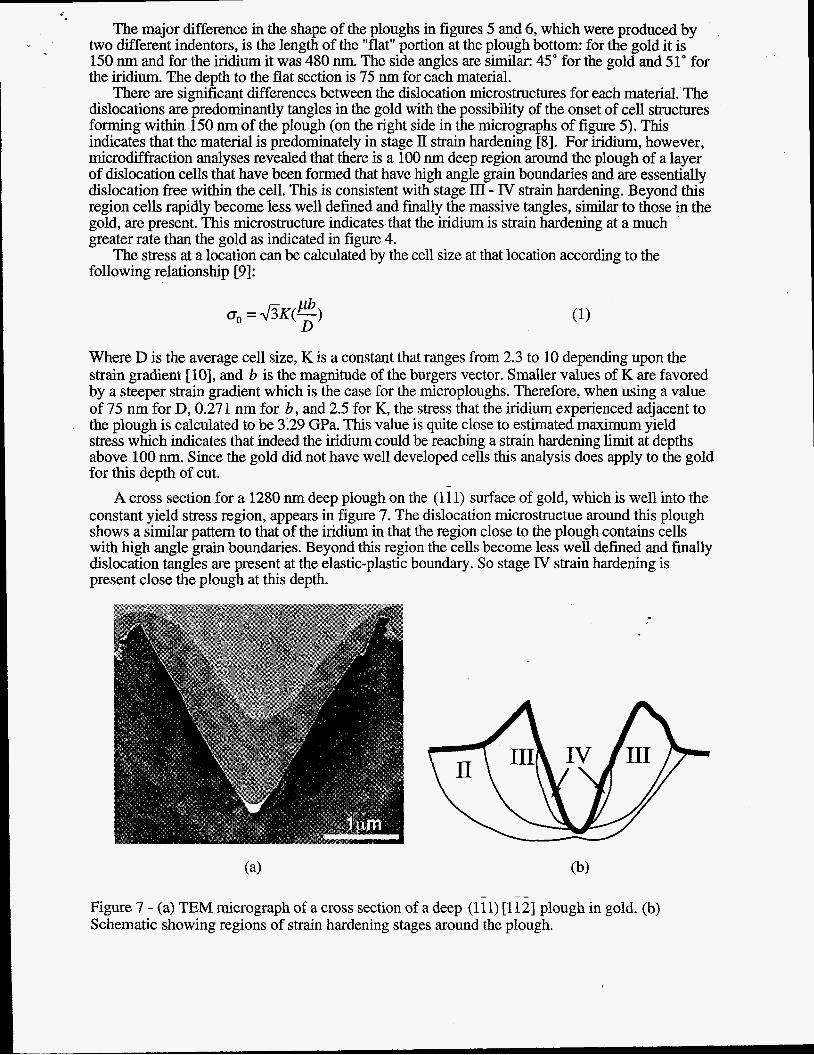
A cross section for a 1280 nm deep plough on the (lil) surface of gold, which is well into the constant yield stress region, appears in figure 7. The dislocation microstructue around this plough shows a similar pattern to that of the iridium in that the region close to the plough contains cells with high angle grain boundaries. Beyond this region the cells become less well defined and finally dislocation tangles are present at the elastic-plastic boundary. So stage IV strain hardening is present close the plough at this depth.
Figure 7 - (a) TEM micrograph of a cross section of a deep (1 i 1) [l i 21 plough in gold. (b) Schematic showing regions of strain hardening stages around the plough.

Using equation (1) and a value of 130 nm for D and 0.288 nm for b gives a calculated yield stress of 266 MPa adjacent to plough. This is well below the estimated maximum strain hardening limit which indicates that the constant yield stress value for gold is caused by a constant average strain.
d.
' .
CONCLUSIONS
These yield stress and TEM data from these microplough experiments indicate that there is no inherent size effect with regard to the ploughing mechanism as was proposed by other researchers [l 11. These data show that in the presence of a stress concentrator, and in the absence of a hard layer at the surface, strain hardening is prevalent even when small volumes of material are involved. Under these conditions, strain hardening theory applies very well, however the severe strain gradient observed around the ploughs does cause added complications that make rigorous analyses difficult.
The TEM data revealed that the iridium is in the final stages of strain hardening near the plough at a 75 nm depth whereas the gold is in the earlier stages at this same depth. Deeper ploughs in gold show that it also hardens into the final stages of strain hardening. Calculations based upon the dislocation cell sizes in the stage IV strain hardened region of the materials show that the stress at this location is greater than the average yield stress calculated from the force data; this result is expected.
hardening ability of the iridium, however in the gold it appears to be caused by a geometrically defined maximum average strain that was achieved.
The constant stress value at larger depths of cut is most likely caused by saturation in the strain
ACKNOWLEDGMENTS
The authors are grateful for the alpha particle scattering analyses performed by Carl Maggiore. We appreciate Doug Hatch's help in building numerous fixtures. Mike Brooks' electropolishing of the samples was crucial to this work. Bob Springer's vacuum annealing of the iridium is highly appreciated. The work of Tracy Woodward and Terry Stark of in generating the TEM cross sections was excellent. The suggestions of Barry Carter were essential in analyzing the TEM samples. Thanks is extended towards Alex Azarkhin who developed the ploughing model.
This work was supported the US. Department of Energy office of Inertial Fusion under contract W7405-ENG-36. The DOE'S funding of this work is also gratefully acknowledged.
REFERENCES
1. M. Abebe and F.C. Appl, Wear, 126, p. 251-283 (1988). 2. K. Nakayama and K. Tamura, J. Eng. Ind., Feb., p. 119-126 (1968). 3. T. Moriwaki and K. Okuda, Annals of ClRP, 38, p. 115-1 18 (1989). 4. G. Petzow, Metallogra&ic Etching: (American Society for Metals, Metals Park, Ohio, 1978),
p. 4 4 microetch b. 1. 5. ibid., p. 43 M1 6. A. Azarkhin, M.D. Devenpeck, Wear, 206, p. 147-155 (1997). 7. A.S. Argon in Physical Metallurm: fourth edition, edited by R.W. Cahn and P. Haasen,
Elsevier science BV, p.1917 (1996). 8 . ibid., p. 1921-1922. 9. ibid., p. 1923. 10. D. Kulmann-Wilsdorf, Scripta Materialia, 34, p. 641-650 (1996). 11. N. Gane and J. Skinner, Wear, 24, p. 207-217 (1973).