xy piezo positioning flexure stages€¦ · xy piezo positioning flexure stages ... newest release...
TRANSCRIPT
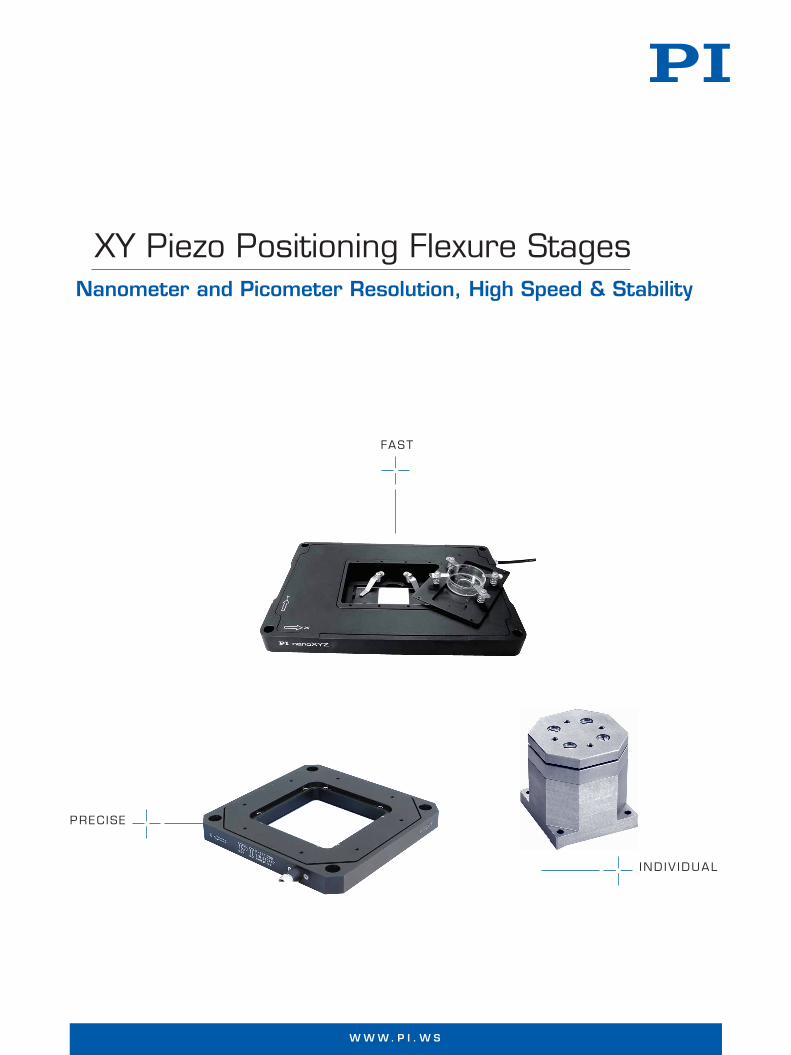
XY Piezo Positioning Flexure StagesNanometer and Picometer Resolution, High Speed & Stability
FAST
PREC ISE
IND IV IDUAL
W W W . P I . W S
XY Piezo Nanopositioning Scanners & Stages
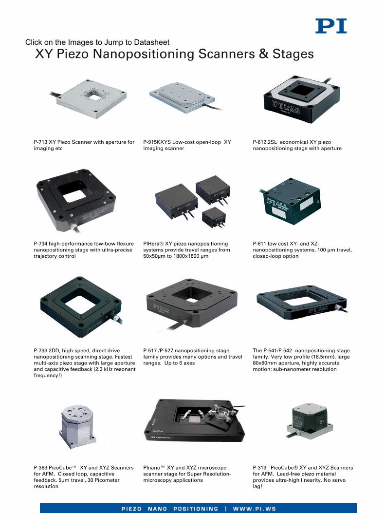
P-713 XY Piezo Scanner with aperture for imaging etc
P-915KXYS Low-cost open-loop XY imaging scanner
P-612.2SL economical XY piezo nanopositioning stage with aperture
P-734 high-performance low-bow flexure nanopositioning stage with ultra-precise trajectory control
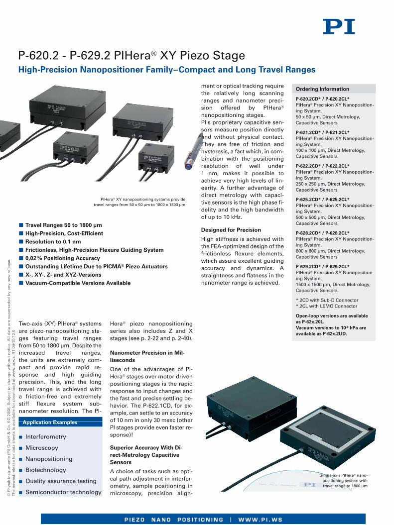
PIHera® XY piezo nanopositioning systems provide travel ranges from 50x50μm to 1800x1800 μm
P-611 low cost XY- and XZ-nanopositioning systems, 100 μm travel, closed-loop option
P-363 PicoCube™ XY and XYZ Scanners for AFM. Closed loop, capacitive feedback. 5µm travel, 30 Picometer resolution
PInano™ XY and XYZ microscope scanner stage for Super Resolution-microscopy applications
P-313 PicoCube® XY and XYZ Scanners for AFM. Lead-free piezo material provides ultra-high linearity. No servo lag!
P-733.2DD, high-speed, direct drive nanopositioning scanning stage. Fastest multi-axis piezo stage with large aperture and capacitive feedback (2.2 kHz resonant frequency!)
P-517 /P-527 nanopositioning stage family provides many options and travel ranges. Up to 6 axes
The P-541/P-542- nanopositioning stage family. Very low profile (16.5mm), large 80x80mm aperture, highly accurate motion: sub-nanometer resolution
Click on the Images to Jump to Datasheet

© P
hys
ik In
stru
men
te (
PI)
Gm
bH
& C
o. K
G 2
008.
Su
bje
ct t
o c
han
ge
wit
ho
ut
no
tice
. All
dat
a ar
e su
per
sed
ed b
y an
y n
ew r
elea
se.
Th
e n
ewes
t re
leas
e fo
r d
ata
shee
ts is
ava
ilab
le f
or
do
wn
load
at
ww
w.p
i.ws.
Cat
120E
Insp
irat
ion
s200
9 08
/10.
18
High-Dynamics Nanoscanner for Scanning Probe Microscopy
P-363 PicoCube™ XY(Z) Piezo Scanner
The P-363 PicoCube™ XY/XYZis an ultra-high-performanceclosed-loop piezo scanningsystem. Designed for AFM,SPM and nanomanipulationapplications, it combines anultra-low inertia, high-speedXY/XYZ piezo scanner withnon-contact, direct-measuring,parallel-metrology capacitivefeedback capable of 50 pico me-ters resolution. On top of beingextremely precise, thePicoCube™ system is also verysmall and rugged. Measuring
only 30 x 30 x 40 mm (withremovable top plate, 30 x 30 x28 mm for XY version), it iseasy to integrate in any scan-ning apparatus.
SPM, AFM, STM, Nano-lithography, Nanoimprinting,
Nanometrology
The PicoCube™ was specifical-ly developed to overcome thelimitations of the open-loopscanners currently available forSPM, AFM and STM. In addi-tion to these applications, thePicoCube™ is also the idealscanning and manipulationtool for nanoimprinting, nano-lithography, ultra-high-resolution, near-field, scanningoptical microscopy and nano-surface-metrology applica-tions.
Higher Precision ThroughParallel-Motion Metrology w/Capacitive Sensors
The PicoCube™ is based on aproprietary, ultra-fast, piezo-driven scanner design equip -
ped with direct-measuring, ca -pacitive position sensors (par -allel metrology). Unlike con-ventional sensors, they meas-ure the actual distance be -tween the fixed frame and themoving part of the stage. Thisresults in higher-motion linear-ity, long-term stability , phasefidelity, and—because externaldisturbances are seen by thesensor immediately—a stiffer ,faster-responding servo-loop.
Multi-axis nanopositioningsystems equipped with paralleldirect metrology are able tomeasure the platform positionin all degrees of freedomagainst one fixed reference. Insuch systems, undesirablemotion from one actuator inthe direction of another (cross-talk) is detected immediatelyand act iv ely compensated bythe servo-loops. This ActiveTra jectory Control Concept cankeep deviation from a trajecto-ry to under a few nanometers,even in dynamic operation.
� Ultra-High-Performance Closed-Loop Scanner for AFM/SPM � Compact Manipulation Tool for Bio/Nanotechnology� Resonant Frequency 9.8 kHz� Capacitive Sensors for Highest Accuracy� Parallel-Motion Metrology for Automated Compensation
of Guiding Errors� 50 Picometer Resolution� 5 x 5 x 5 µm Travel Range� Vacuum-Compatible Versions
P-363.2CD and .3CD (background)PicoCube™, high-performancepiezo positioning- and scanningsystems or AFM/STM andnanomanipulation. Smart mediacard for size comparison
Application Examples
� Scanning microscopy(SPM)
� Biotechnology
� Micromanipulation
� Nanopositioning
� Nano-imprinting
� Nanometrology
� Nanolithography
Ordering Information
P-363.3CDPicoCube™ High-Precision XYZNanopositioning System, 5 x 5 x 5 µm, Parallel Metrology ,Capacitive Sensors, Sub-DConnector
P-363.3UDPicoCube™ High-Precision XYZNanopositioning System, 5 x 5 x 5 µm, Parallel Metrology ,Capacitive Sensors, Sub-DConnector, Vacuum Compatible to 10-9 hPa
P-363.2CDPicoCube™ High-Precision XYNanopositioning System, 5 x 5 µm,Parallel Metrology, CapacitiveSensors, Sub-D Connector
P-363.2UDPicoCube™ High-Precision XYNanopositioning System, 5 x 5 µm,Parallel Metrology, CapacitiveSensors, Sub-D Connector, VacuumCompatible to 10-9 hPa
P-363.3CLPicoCube™ High-Precision XYZNanopositioning System, 5 x 5 x 5 µm, Parallel Metrology ,Capacitive Sensors, LEMOConnector
P-363.2CLPicoCube™ High-Precision XYNanopositioning System, 5 x 5 µm,Parallel Metrology, CapacitiveSensors, LEMO Connector
300 picometersteps (0.3 nm)performed withthe P-363, meas-ured with anexternal high-resolution,capacitive meas-urement system
The P-363 settlesto within 1 nm in1 ms (100 nmstep, X and Ymotion; fasterresponse in Z)
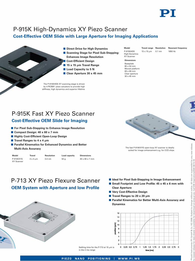
P-915K Fast XY Piezo ScannerCost-Effective OEM Slide for Imaging
� For Pixel Sub-Stepping to Enhance Image Resolution� Compact Design: 40 x 60 x 7 mm� Highly Cost-Efficient Open-Loop Design� Travel Ranges to 4 x 4 µm� Parallel Kinematics for Enhanced Dynamics and Better
Multi-Axis Accuracy
Model Travel Resolution Load capacity Dimensions
P-915KXYS 4 x 4 µm 0.4 nm 50 g 40 x 60 x 7 mmXY Scanner
P-915K High-Dynamics XY Piezo ScannerCost-Effective OEM Slide with Large Aperture for Imaging Applications
� Direct Drive for High Dynamics� Scanning Stage for Pixel Sub-Stepping:
Enhances Image Resolution� Cost-Efficient Design� 15 x 15 µm Travel Range� Load Capacity to 5 N� Clear Aperture 30 x 45 mm
Model Travel range Resolution Resonant frequency
P-915KHDS 15 x 15 µm 0.1 nm 1850 HzHigh-DynamicsXY Scanner
Dimensions
Baseplate85 x 54 mmMoved platform69 x 69 mmClear aperture30 x 45 mm
©P
hys
ikIn
stru
men
te(P
I)G
mb
H&
Co
.KG
2008
.Su
bje
ctto
chan
ge
wit
ho
ut
no
tice
.All
dat
aar
esu
per
sed
edb
yan
yn
ewre
leas
e.T
he
new
est
rele
ase
for
dat
ash
eets
isav
aila
ble
for
do
wn
load
atw
ww
.pi.w
s.C
at12
0EIn
spir
atio
ns2
009
08/1
0.18
P-713 XY Piezo Flexure ScannerOEM System with Aperture and low Profile
� Ideal for Pixel Sub-Stepping in Image Enhancement� Small Footprint and Low Profile: 45 x 45 x 6 mm with
Clear Aperture� Very Cost-Effective Design� Travel Ranges to 20 x 20 µm� Parallel Kinematics for Better Multi-Axis Accuracy and
Dynamics
Settling time for the P-713 at 15 µm isin the 2 ms range
The fast P-915KXYS open-loop XY scanner is ideallysuited for image enhancement e.g. for CCD chips
The P-915KHDS XY scanning stage is drivenby 4 PICMA® piezo actuators to provide high
stiffness, high dynamics and superior lifetime
©P
hys
ikIn
stru
men
te(P
I)G
mb
H&
Co
.KG
2008
.Su
bje
ctto
chan
ge
wit
ho
ut
no
tice
.All
dat
aar
esu
per
sed
edb
yan
yn
ewre
leas
e.T
he
new
est
rele
ase
for
dat
ash
eets
isav
aila
ble
for
do
wn
load
atw
ww
.pi.w
s.R
110
/11/
08.0
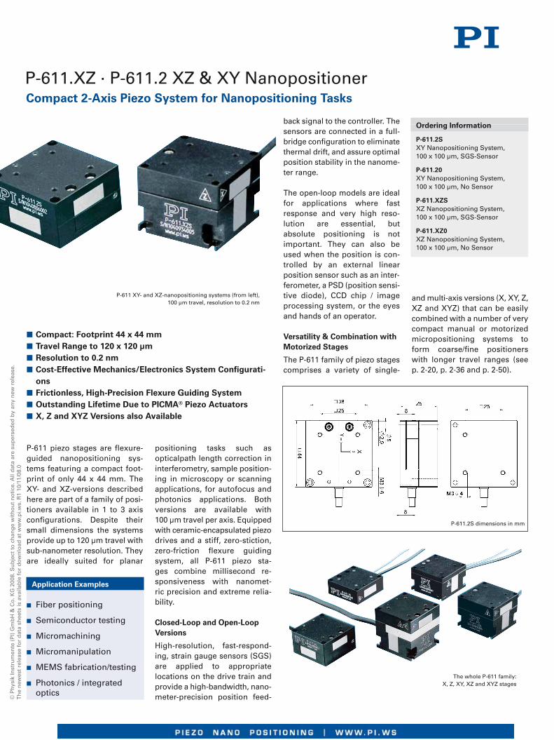
P-611.XZ · P-611.2 XZ & XY NanopositionerCompact 2-Axis Piezo System for Nanopositioning Tasks
P-611 piezo stages are flexure-guided nanopositioning sys-tems featuring a compact foot-print of only 44 x 44 mm. TheXY- and XZ-versions describedhere are part of a family of posi-tioners available in 1 to 3 axisconfigurations. Despite theirsmall dimensions the systemsprovide up to 120 µm travel withsub-nanometer resolution. Theyare ideally suited for planar
positioning tasks such asopticalpath length correction ininterferometry, sample position-ing in microscopy or scanningapplications, for autofocus andphotonics applications. Bothversions are available with100 µm travel per axis. Equippedwith ceramic-encapsulated piezodrives and a stiff, zero-stiction,zero-friction flexure guidingsystem, all P-611 piezo sta-ges combine millisecond re-sponsiveness with nanomet-ric precision and extreme relia-bility.
Closed-Loop and Open-LoopVersions
High-resolution, fast-respond-ing, strain gauge sensors (SGS)are applied to appropriatelocations on the drive train andprovide a high-bandwidth, nano-meter-precision position feed-
back signal to the controller. Thesensors are connected in a full-bridge configuration to eliminatethermal drift, and assure optimalposition stability in the nanome-ter range.
The open-loop models are idealfor applications where fastresponse and very high reso-lution are essential, butabsolute positioning is notimportant. They can also beused when the position is con-trolled by an external linearposition sensor such as an inter-ferometer, a PSD (position sensi-ive diode), CCD chip / image
processing system, or the eyesand hands of an operator.
Versatility & Combination withMotorized Stages
The P-611 family of piezo stagescomprises a variety of single-
and multi-axis versions (X, XY, Z,XZ and XYZ) that can be easilycombined with a number of verycompact manual or motorizedmicropositioning systems toform coarse/fine positionerswith longer travel ranges (seep. 2-20, p. 2-36 and p. 2-50).
Application Examples
� Fiber positioning
� Semiconductor testing
� Micromachining
� Micromanipulation
� MEMS fabrication/testing
� Photonics / integratedoptics
Ordering Information
P-611.2SXY Nanopositioning System,100 x 100 µm, SGS-Sensor
P-611.20XY Nanopositioning System,100 x 100 µm, No Sensor
P-611.XZSXZ Nanopositioning System,100 x 100 µm, SGS-Sensor
P-611.XZ0XZ Nanopositioning System,100 x 100 µm, No Sensor
P-611 XY- and XZ-nanopositioning systems (from left), t100 µm travel, resolution to 0.2 nm
� Compact: Footprint 44 x 44 mm� Travel Range to 120 x 120 µm� Resolution to 0.2 nm� Cost-Effective Mechanics/Electronics System Configurati-
ons� Frictionless, High-Precision Flexure Guiding System� Outstanding Lifetime Due to PICMA® Piezo Actuators� X, Z and XYZ Versions also Available
The whole P-611 family:X, Z, XY, XZ and XYZ stages
P-611.2S dimensions in mm

Technical Data
Model P-611.2S P-611.20 P-611.XZS P-611.XZ0 Units Tolerance
Active axes X, Y X, Y X, Z X, Z
Motion and positioning
Integrated sensor SGS – SGS –
Open-loop travel, -20 to +120 V 120 120 120 120 µm min. (+20 %/0 %)
Closed-loop travel 100 – 100 – µm
Open-loop resolution 0.2 0.2 0.2 0.2 nm typ.
Closed-loop resolution 2 – 2 – nm typ.
Linearity 0.1 – 0.1 – % typ.
Repeatability <10 – <10 – nm typ.
Pitch in X,Y ±5 ±5 ±5 ±5 µrad typ.
Runout θX (Z motion) – – ±10 ±10 µrad typ.
Yaw in X ±20 ±20 ±20 ±20 µrad typ.
Yaw in Y ±10 ±10 – – µrad typ.
Runout θY (Z motion) – – ±10 +/-10 µrad typ.
Mechanical properties
Stiffness 0.2 0.2 0.2 0.2 N/µm ±20 %Z: 0.35 Z: 0.35
Unloaded resonant frequency X: 345; Y: 270 X: 345; Y: 270 X: 365; Z: 340 X: 365; Z: 340 Hz ±20 %
Resonant frequency @ 30 g X: 270; Y: 225 X: 270; Y: 225 X: 280; Z: 295 X: 280; Z: 295 Hz ±20 %
Resonant frequency @ 100 g X: 180; Y: 165 X: 180; Y: 165 X: 185; Z: 230 X: 185; Z: 230 Hz ±20 %
Push/pull force capacity 15 / 10 15 / 10 15 / 10 15 / 10 N Max.in motion direction
Load capacity 15 15 15 15 N Max.
Drive properties
Ceramic type PICMA® P-885 PICMA® P-885 PICMA® P-885 PICMA® P-885
Electrical capacitance 1.5 1.5 1.5 1.5 µF ±20 %
Dynamic operating current coefficient 1.9 1.9 1.9 1.9 µA/(Hz • µm) ±20 %
Miscellaneous
Operating temperature range -20 to 80 -20 to 80 -20 to 80 -20 to 80 °C
Material Aluminum, steel Aluminum, steel Aluminum, steel Aluminum, steel
Dimensions 44 x 44 x 25 44 x 44 x 25 44 x 44 x 34 44 x 44 x 34 mm
Mass 0.235 0.235 0.27 0.27 kg ±5 %
Cable length 1.5 1.5 1.5 1.5 m ±10 mm
Sensor connection LEMO – LEMO –
Voltage connection LEMO LEMO LEMO LEMO
Resolution of PI Piezo Nanopositioners is not limited by friction or stiction. Value given is noise equivalent motion with E-503 amplifier (p. 2-146)Dynamic Operating Current Coefficient in µA per Hz and µm. Example: Sinusoidal scan of 50 µm at 10 Hz requires approximately 0.9 mA drive current.Recommended controller / amplifierSingle-channel (1 per axis): E-610 servo controller / amplifier (p. 2-110), E -625 servo controller, bench-top (p. 2-114), E-621 controller module (p. 2-160)Multi-channel: modular piezo controller system E-500 (p. 2-142) with amplifier module E-503 (three channels) (p. 2-146) or E-505 (1 per axis, high-power) (p. 2-147) and E-509controller (p. 2-152)
P-611.XZS dimensions in mm
©P
hys
ikIn
stru
men
te(P
I)G
mb
H&
Co
.KG
2008
.Su
bje
ctto
chan
ge
wit
ho
ut
no
tice
.All
dat
aar
esu
per
sed
edb
yan
yn
ewre
leas
e.T
he
new
est
rele
ase
for
dat
ash
eets
isav
aila
ble
for
do
wn
load
atw
ww
.pi.w
s.R
109
/10/
12.0
Two-axis (XY) PIHera® systemsare piezo-nanopositioning sta-ges featuring travel rangesfrom 50 to 1800 µm. Despite theincreased travel ranges,the units are extremely com-pact and provide rapid re-sponse and high guidingprecision. This, and the longtravel range is achieved witha friction-free and extremelystiff flexure system sub-nanometer resolution. The PI-
Hera® piezo nanopositioningseries also includes Z and Xstages (see p. 2-22 and p. 2-40).
Nanometer Precision in Mil-liseconds
One of the advantages of PI-Hera® stages over motor-drivenpositioning stages is the rapidresponse to input changes andthe fast and precise settling be-havior. The P-622.1CD, for ex-ample, can settle to an accuracyof 10 nm in only 30 msec (otherPI stages provide even faster re-sponse)!
Superior Accuracy With Di-rect-Metrology CapacitiveSensors
A choice of tasks such as opti-cal path adjustment in interfer-ometry, sample positioning inmicroscopy, precision align-
ment or optical tracking requirethe relatively long scanningranges and nanometer preci-sion offered by PIHera®
nanopositioning stages.PI's proprietary capacitive sen-sors measure position directlyand without physical contact.They are free of friction andhysteresis, a fact which, in com-bination with the positioningresolution of well under1 nm, makes it possible toachieve very high levels of lin-earity. A further advantage ofdirect metrology with capaci-tive sensors is the high phase fi-delity and the high bandwidthof up to 10 kHz.
Designed for Precision
High stiffness is achieved withthe FEA-optimized design of thefrictionless flexure elements,which assure excellent guidingaccuracy and dynamics. Astraightness and flatness in thenanometer range is achieved.
Application Examples
� Interferometry
� Microscopy
� Nanopositioning
� Biotechnology
� Quality assurance testing
� Semiconductor technology
Ordering Information
P-620.2CD* / P-620.2CL*PIHera® Precision XY Nanoposition-ing System,50 x 50 µm, Direct Metrology,Capacitive Sensors
P-621.2CD* / P-621.2CL*PIHera® Precision XY Nanoposition-ing System,100 x 100 µm, Direct Metrology,Capacitive Sensors
P-622.2CD* / P-622.2CL*PIHera® Precision XY Nanoposition-ing System,250 x 250 µm, Direct Metrology,Capacitive Sensors
P-625.2CD* / P-625.2CL*PIHera® Precision XY Nanoposition-ing System,500 x 500 µm, Direct Metrology,Capacitive Sensors
P-628.2CD* / P-628.2CL*PIHera® Precision XY Nanoposition-ing System,800 x 800 µm, Direct Metrology,Capacitive Sensors
P-629.2CD* / P-629.2CL*PIHera® Precision XY Nanoposition-ing System,1500 x 1500 µm, Direct Metrology,Capacitive Sensors
*.2CD with Sub-D Connector*.2CL with LEMO Connector
Open-loop versions are availableas P-62x.20L.Vacuum versions to 10-9 hPa areavailable as P-62x.2UD.
High-Precision Nanopositioner Family–Compact and Long Travel Ranges
P-620.2 - P-629.2 PIHera® XY Piezo Stage
PIHera® XY nanopositioning systems providetravel ranges from 50 x 50 µm to 1800 x 1800 µm
� Travel Ranges 50 to 1800 µm� High-Precision, Cost-Efficient� Resolution to 0.1 nm� Frictionless, High-Precision Flexure Guiding System� 0,02 % Positioning Accuracy� Outstanding Lifetime Due to PICMA® Piezo Actuators� X-, XY-, Z- and XYZ-Versions� Vacuum-Compatible Versions Available
Single-axis PIHera® nano-positioning system withtravel range to 1800 µm

Technical Data
Model P-620.2CD/ P-621.2CD/ P-622.2CD/ P-625.2CD/ P-628.2CD/ P-629.2CD P-62x.20L Units ToleranceP-620.2CL P-621.2CL P-622.2CL P-625.2CL P-628.2CL P-629.2CL open-loop versions
Active axes X, Y X, Y X, Y X, Y X, Y X, Y X, Y
Motion and positioning
Integrated sensor Capacitive Capacitive Capacitive Capacitive Capacitive Capacitive –
Open-loop travel X, Y, -20 to +120 V 60 120 300 600 950 1800 as P-62x.2CD µm min. (+20 %/-0 %)
Closed-loop travel 50 100 250 500 800 1500 – µm
Open-loop resolution 0.1 0.2 0.4 0.5 0.5 2 as P-62x.2CD nm typ.
Closed-loop resolution 0.2 0.4 0.7 1.4 3.5 3.5 – nm typ.
Linearity 0.02 0.02 0.02 0.03 0.03 0.03 – % typ.
Repeatability ±2 ±2 ±2 ±5 ±10 ±14 as P-62x.2CD nm typ.
Pitch / yaw ±3 ±3 ±3 ±3 ±20 ±30 as P-62x.2CD µrad typ.
Mechanical properties
Stiffness 0.22 0.25 0.2 0.1 0.05 0.1 as P-62x.2CD N/µm ±20 %
Unloaded resonant frequency in X, 575 420 225 135 75 60 as P-62x.2CD Hz ±20 %
Unloaded resonant frequency in Y 800 535 300 195 105 100 as P-62x.2CD Hz ±20 %
Resonant frequency in X @ 50 g 270 285 180 120 60 55 as P-62x.2CD Hz ±20 %
Resonant frequency in Y @ 50 g 395 365 215 150 85 85 as P-62x.2CD Hz ±20 %
Resonant frequency in X @ 100 g 285 220 160 105 55 50 as P-62x.2CD Hz ±20 %
Resonant frequency in Y @ 100 g 300 285 175 125 75 80 as P-62x.2CD Hz ±20 %
Push/pull force capacity in motion direction 10 / 5 10 / 8 10 / 8 10 / 8 10 / 8 10 / 8 as P-62x.2CD N Max.
Load capacity 10 10 10 10 10 10 as P-62x.2CD N Max.
Lateral Force 10 10 10 10 10 10 as P-62x.2CD N Max.
Drive properties
Ceramic type PICMA® P-883 PICMA® P-885 PICMA® P-885 PICMA® P-885 PICMA® P-887 PICMA® P-888 as P-62x.2CD
Electrical Capacitance 0.35 1.5 3.1 6.2 19 52 as P-62x.2CD µF ±20 %
Dynamic operating current coefficient 0.9 1.9 1.9 1.6 3 4.3 as P-62x.2CD µA/(Hz•µm) ±20 %
Miscellaneous
Operating temperature range -20 to 80 -20 to 80 -20 to 80 -20 to 80 -20 to 80 -20 to 80 -20 to 150 °C
Material Aluminum Aluminum Aluminum Aluminum Aluminum Aluminum Aluminum
Mass 0.195 0.295 0.348 0.43 0.7 1.37 as P-62x.2CD kg ±5 %
Cable length 1.5 1.5 1.5 1.5 1.5 1.5 1.5 m ±10 mm
Sensor / voltage connection CD version: CD version: CD version: CD version: CD version: CD version: 2x LEMO2x Sub-D special 2x Sub-D special 2x Sub-D special 2x Sub-D special 2x Sub-D special 2x Sub-D special (no sensor)CL version: CL version: CL version: CL version: CL version: CL version:LEMO LEMO LEMO LEMO LEMO LEMO
Lower axis: X; upper axis: Y.Resolution of PI Piezo Nanopositioners is not limited by friction or stiction. The value given is noise equivalent motion with E-710 controller (p. 2-128)Recommended controllerCD version: E-610 servo controller / amplifier (p. 2-110), E-625 servo controller, bench-top (p. 2-114), E-665 powerful servo controller, bench-top (p. 2-116)
Multi-channel digital controllers: E-710 bench-top (p. 2-128), E-712 modular (p. 2-140), E-725 high-power (p. 2-126), E-761 PCI board (p. 2-140)CL version: E-500 modular piezo controller system (p. 2-142) with E-505 amplifier module (1 per axis, high power) (p. 2-147) and E-509 controller (p. 2-152)Open-loop versions: E-500 modular piezo controller system (p. 2-142) with E-505 amplifier module (1 per axis, high power) (p. 2-147)
P-62x.2CD/.2CL/.20L dimensions in mm
© P
hys
ik In
stru
men
te (
PI)
Gm
bH
& C
o. K
G 2
008.
Su
bje
ct t
o c
han
ge
wit
ho
ut
no
tice
. All
dat
a ar
e su
per
sed
ed b
y an
y n
ew r
elea
se.
Th
e n
ewes
t re
leas
e fo
r d
ata
shee
ts is
ava
ilab
le f
or
do
wn
load
at
ww
w.p
i.ws.
Cat
120E
Insp
irat
ion
s200
9 08
/10.
18
P-612 XY Piezo Nanopositioning SystemCompact, Clear Aperture
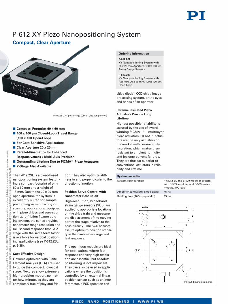
The P-612.2SL is a piezo-basednanopositioning system featur -ing a compact footprint of only60 x 60 mm and a height of 18 mm. Due to the 20 x 20 mmopen aperture, the system isexcellently suited for samplepositioning in microscopy orscanning applications. Equip p edwith piezo drives and zero-stic-tion, zero-friction flexure guid-ing system, the series providesnanometer-range resolution andmillisecond response time. A Zstage with the same form factoris available for vertical position-ing applications (see P-612.ZSLp. 2-38).
Cost-Effective Design
Flexures optimized with FiniteElement Analysis (FEA) are usedto guide the compact, low-coststage. Flexures allow extremelyhigh-precision motion, no mat-ter how minute, as they arecompletely free of play and fric-
tion. They also optimize stiff-ness in and perpendicular to thedirection of motion.
Position Servo-Control withNanometer Resolution
High-resolution, broadband,strain gauge sensors (SGS) areapplied to appropriate locationson the drive train and measurethe displacement of the movingpart of the stage relative to thebase directly. The SGS sensorsassure optimum position stabili-ty in the nanometer range andfast response.
The open-loop models are idealfor applications where fastresponse and very high resolu-tion are essential, but absolutepositioning is not important.They can also be used in appli-cations where the position iscontrolled by an external linearposition sensor such as an inter-ferometer, a PSD (position sen-
sitive diode), CCD chip / imageprocessing system, or the eyesand hands of an operator.
Ceramic Insulated PiezoActuators Provide LongLifetime
Highest possible reliability isassured by the use of award-winning PICMA ® multilayerpiezo actuators. PICMA ® actua-tors are the only actuators onthe market with ceramic-onlyinsulation, which makes themresistant to ambient humidityand leakage-current failures.They are thus far superior toconventional actuators in relia-bility and lifetime.
Ordering Information
P-612.2SLXY Nanopositioning System with 20 x 20 mm Aperture, 100 x 100 µm,Strain Gauge Sensors
P-612.20LXY Nanopositioning System withAperture 20 x 20 mm, 100 x 100 µm,Open-Loop
P-612.2SL XY piezo stage (CD for size comparison)
� Compact: Footprint 60 x 60 mm� 100 x 100 µm Closed-Loop Travel Range
(130 x 130 Open-Loop)� For Cost-Sensitive Applications� Clear Aperture 20 x 20 mm� Parallel-Kinematics for Enhanced
Responsiveness / Multi-Axis Precision� Outstanding Lifetime Due to PICMA® Piezo Actuators� Z-Stage Also Available
System properties
System configuration P-612.2 SL and E-500 modular systemwith E-503 amplifier and E-509 sensormodule, 100 load
Amplifier bandwidth, small signal 45 Hz
Settling time (10 % step width) 15 ms
P-612.2 dimensions in mm
Technical Data
Model P-612.2SL P-612.20L Units Tolerance
Active axes X, Y X, Y
Motion and positioning
Integrated sensor SGS –
Open-loop travel, -20 to +120 V 130 130 µm min. (+20 %/-0 %)
Closed-loop travel 100 – µm
Open-loop resolution 0.8 0.8 nm typ.
Closed-loop resolution 5 – nm typ.
Linearity 0.4 – % typ.
Repeatability <10 – nm typ.
Pitch ±10 ±10 µrad typ.
Yaw in X/ Y ±10 / ±50 ±10 / ±50 µrad typ.
Mechanical properties
Stiffness 0.15 0.15 N/µm ±20 %
Unloaded resonant frequency 400 400 Hz ±20 %
Resonant frequency @ 100 g 200 200 Hz ±20 %
Push/pull force capacity in motion direction 15 / 5 15 / 5 N Max.
Load capacity 15 15 N Max.
Drive properties
Ceramic type PICMA® P-885 PICMA® P-885
Electrical capacitance 1.5 1.5 µF ±20 %
Dynamic operating current coefficient 1.9 1.9 µA/(Hz • µm) ±20 %
Miscellaneous
Operating temperature range -20 to 80 -20 to 80 °C
Material Aluminum, steel Aluminum, steel
Mass 105 105 g ±5 %
Cable length 1.5 1.5 m ±10 mm
Sensor connector LEMO connector –
Voltage connection LEMO connector LEMO connector
Resolution of PI Piezo Nanopositioners is not limited by friction or stiction. Noise equivalent motion with E-503 amplifier (p. 2-146)Recommended controllerSingle-channel (1 per axis): E-610 servo-controller / amplifier (p. 2-110) , E-625 servo-controller, bench-top (p. 2-114), E-621 controller module (p. 2-160)Multi-channel: modular piezo controller system E-500 (p. 2-142) with amplifier module E-503 (three channels) (p. 2-146) or E-505 (1 per axis, high-power) (p. 2-147) and E-509 controller (p. 2-152)
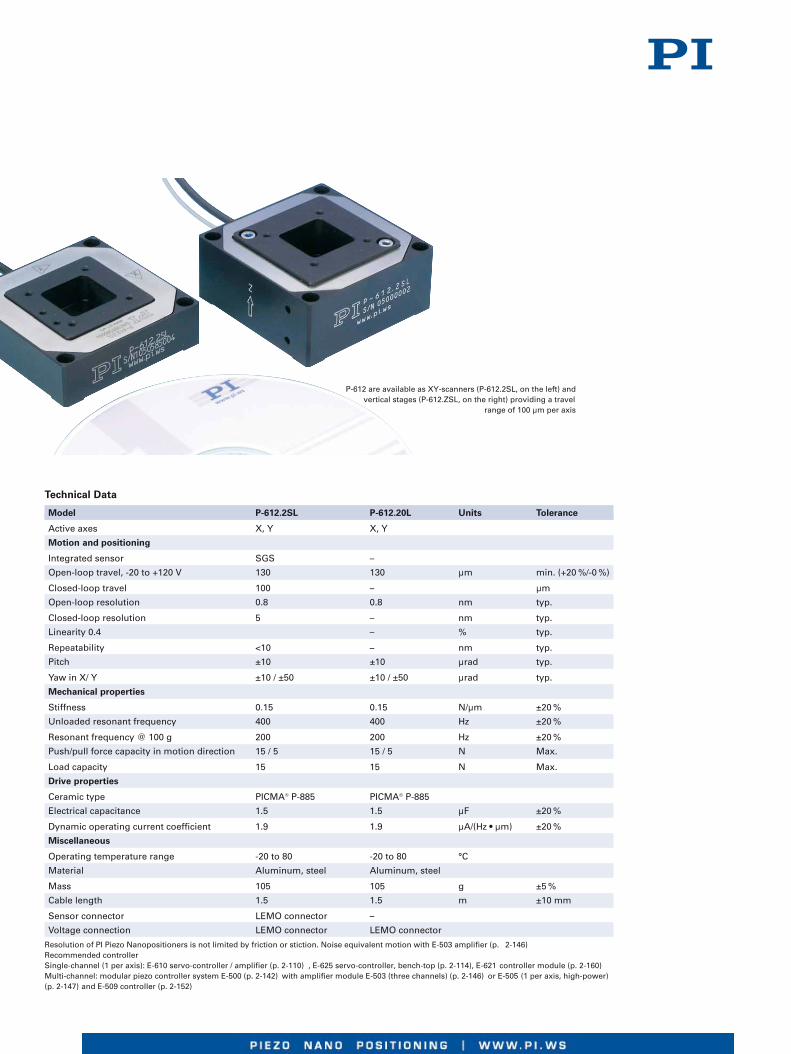
P-612 are available as XY-scanners (P-612.2SL, on the left) andvertical stages (P-612.ZSL, on the right) providing a travel
range of 100 µm per axis

Low-Profile, Low-Cost Nanopositioning Systems for Super-Resolution Microscopy
P-545 PI nano™
Long Travel, Low Profile,Optimized for MicroscopyPI nano™ XY and XYZ low-pro-file piezo scanning stages areoptimized for easy integrationinto high-resolution micro-
scopes. They feature a very lowprofile of 20 mm (0.8") and alarge aperture designed to holdPetri dishes and standard slideholders. The long travel rangesof up to 200 x 200 x 200 µm withnanometer closed-loop resolu-tion are ideal for leading-edge
microscopy and imaging appli-cations.
Cost Effective Design,High Performance
PI nano™ series piezo position-ing stages are designed to pro-vide high performance atminimum cost. For highly-sta-ble, closed loop operation,piezoresistive sensors are ap-plied directly to the movingstructure and precisely meas-ure the displacement of thestage platform. The very highsensitivity of these sensors pro-vides optimum position stabil-ity and responsiveness as wellas nanometer resolution. A pro-prietary servo controller signifi-cantly improves the motionlinearity compared to conven-tional piezoresistive sensorcontrollers.
High Reliability andLong Lifetime
The compact P-545 systems areequipped with preloaded PIC-MA® high-performance piezoactuators which are integratedinto a sophisticated, FEA-mod-eled, flexure guiding system.The PICMA® actuators featurecofired ceramic encapsulationand provide better performanceand reliability than conven-tional piezo actuators. Actua-tors, guidance and sensors aremaintenance-free, not subjectto wear and offer extraordinaryreliability.
� Low Profile for Easy Integration: 20 mm (0.8'')� XY and XYZ Versions 200 µm Travel Range� Large Clear Aperture for 3 x 1'' Slides� Recessed Sample Holders for Maximized Utility Available� Outstanding Lifetime Due to PICMA®Piezo Actuators� Cost-Effective Design due to Piezoresistive Sensors� Compatible w/ Leading Image Acquisition Software Package� Closed-Loop Control for High Repeatability and Accuracy� Millisecond Step Time, Ideal for Super-Resolution Microscopy� 24-Bit Controller w/ USB, Ethernet, RS-232 Interface
and Analog Control� Available Manual Long-Travel Stage with Motor
Upgrade Option
Application Examples
� Super-resolutionmicroscopy
� 3D Imaging
� Laser technology
� Interferometry
� Metrology
� Biotechnology
� Screening
� Micromanipulation
PI nano™series nanopositioning stages feature a very low profile of 20 mm (0.8),a large aperture for 3 x 1'' slides and deliver highly accurate motion with
sub-nanometer resolution Slide / petri dish holders optional
Ordering Information
P-545.2R7PInano™ XY Piezo Stage, Slide-SizeAperture, 200 x 200 µm, Piezoresis-tive Sensors, with USB Controller
Controller included
E-545.3RDPInano™ Multi-Channel PiezoController with High-Speed DigitalInterface, 3 Channels, PiezoresistivSensors, Sub-D Connectors
Accessories
M-545.2MOXY Microscope Stage, 25 x 25 mm,Micrometer-Driven, High Stability,Compatible with PI® Piezo Stages,for Olympus Microscopes
M-545.2MNXY Microscope Stage, 25 x 25 mm,Micrometer-Driven, High Stability,Compatible with PI® Piezo Stages,for Nikon Microscopes
M-545.2MLXY Microscope Stage, 25 x 25 mm,Micrometer-Driven, High Stability,Compatible with PI® Piezo Stages,for Leica Microscopes
M-545.2MZXY Microscope Stage, 25 x 25 mm,Micrometer-Driven, High Stability,Compatible with PI® Piezo Stages,for Zeiss Microscope
P-545.PD335mm Petri Dish Holder for P-545PInano™ Piezo Stages
P-545.SH3Microscope Slide Holder forPInano™ Piezo Stages
P-545.PP3Plain Plate for Accessories forPInano™ Piezo Stages
Additional accessories on request.
e
©P
hys
ikIn
stru
men
te(P
I)G
mb
H&
Co
.KG
2009
.Su
bje
ctto
chan
ge
wit
ho
ut
no
tice
.All
dat
aar
esu
per
sed
edb
yan
yn
ewre
leas
e.T
he
new
est
rele
ase
for
dat
ash
eets
isav
aila
ble
for
do
wn
load
atw
ww
.pi.w
s.R
310
/05/
05.0
Background: the piezo controlleris included and comes with a 24-bit
resolution USB port as well as ethernet,RS-232 and analog interface.
Foreground: The optional M-545 manualXY stage provides a stable
platform for the PI nano™ piezo stages.Custom stage version shown
XY Piezo Stage for SR Microscopy

Technical Data
Model P-545.2R7
Active axes X, Y
Motion and positioning
Integrated sensor piezoresistive
Closed-loop travel 200 x 200
Closed-loop resolution* 1
Linearity ±0.1
Repeatability < 5
Mechanical properties
Push/pull force capacity 100 / 30
Load 50
Drive properties
Ceramic type PICMA® P-885
Electrical capacitance 6
Miscellaneous
Operating temperature range -20 to 80
Material Aluminum
Mass 1
Cable length 1.5
Sensor / voltage connection Sub-D, 25 pin
Piezo controller (included in delivery) E-545
* Resolution of PI Piezo Nanopositioners is not limited by friction or stiction. Value given is noise equivalent motion measured with interferometer.
Accessories: Slide holder (above) and Petri dishholder (below), dimensions in mm P-545 dimensions in mm
Unit Tolerance
µm
nm typ.
% typ.
nm typ.
N max.
N max.
µF ±20%
°C
kg ±5%
m ±10 mm
Capacitive Sensor Version and High Speed Tracking Version also Available

©P
hys
ikIn
stru
men
te(P
I)G
mb
H&
Co
.KG
2008
.Su
bje
ctto
chan
ge
wit
ho
ut
no
tice
.All
dat
aar
esu
per
sed
edb
yan
yn
ewre
leas
e.T
he
new
est
rele
ase
for
dat
ash
eets
isav
aila
ble
for
do
wn
load
atw
ww
.pi.w
s.R
310
/10/
04.0
P-541.2 – P-542.2 Piezo XY-StageLow-Profile XY Nanopositioning System with Large Aperture
Low Profile, Optimized forMicroscopy Applications
P-541/P-542 nanopositioning andscanning stages are designed foreasy integration into high-resolu-tion microscopes. They feature avery low profile of 16.5 mm, alarge 80 x 80 mm aperture, andoffer highly accurate motion withsub-nanometer resolution.A variety of Z stages andZ-tip/tilt stages with the samefootprint are also offered to suit awide range of applications
(p. 2-44). They are ideal for align-ment, nano-focusing or metrol-ogy tasks.
Choice of Drives: Long Range orHigh-Speed Direct Drive
Lever-amplified XY systems with100 and 200 µm travel anddirect-driven XY scanners with45 µm travel are available. Theirhigh resonant frequencies of1.5 kHz in both axes allowfor faster step response andhigher scanning rates, needed forexample in single-molecule mi-croscopy, or in other time-criticalapplications.
Parallel Kinematics for Fast Re-sponse
In a parallel kinematics multi-axissystem, all actuators act directlyon one moving platform. Thismeans that all axes move thesame minimized mass and canbe designed with identical dy-namic properties. Systems with
parallel kinematics and metrol-ogy have additional advantagesover serially stacked or nestedsystems, including more-com-pact construction and no cumula-tive error from the different axes.Parallel kinematics systems canbe operated with up to six de-grees of freedom with low inertiaand excellent dynamic perform-ance. Multi-axis nanopositioningsystems equipped with both par-allel kinematics and parallel, di-rect metrology are able tomeasure platform position in alldegrees of freedom against onecommon fixed reference. In suchsystems, undesirable motionfrom one actuator in the directionof another (cross talk) is detectedimmediately and actively com-pensated by the servo-loops.
Tailored Position Measurement
Integrated high-resolution posi-tion sensors provide fast re-sponse and positional stabilityin the nanometer range. Top-of-the-line models use capacitivesensors. They measure displace-ment directly and withoutphysical contact (direct metrol-ogy) enabling superior linearity.Alternatively, versions with cost-effective strain gauge sensors(SGS) are also available.
Application Examples
� Laser technology
� Scanning microscopy
� Mask / wafer positioning
� Interferometry
� Metrology
� Biotechnology
� Micromanipulation
Ordering Information
P-541.2DDXY Nanopositioning System withLarge Aperture, High-Speed DirectDrive, 45 x 45 µm, Parallel Kinemat-ics, Capacitive Sensors
P-541.2CDXY Nanopositioning System withLarge Aperture, 100 x 100 µm, Paral-lel Kinematics, Capacitive Sensors
P-542.2CD / P-542.2CLXY Nanopositioning System withLarge Aperture, 200 x 200 µm, Paral-lel Kinematics, Capacitive Sensors
P-541.2SLXY Nanopositioning System withLarge Aperture, 100 x 100 µm,Strain Gauge Sensors
P-542.2SLXY Nanopositioning System withLarge Aperture, 200 x 200 µm,Strain Gauge Sensors
P-541.20LXY Nanopositioning System withLarge Aperture, 100 x 100 µm,Open Loop
P-542.20LXY Nanopositioning System withLarge Aperture, 200 x 200 µm,Open Loop
� Low Profile for Easy Integration: 16.5 mm; 80 x 80 mmClear Aperture
� Up to 200 x 200 µm Travel Range� Parallel-Kinematics / Metrology for Enhanced
Responsiveness & Multi-Axis Precision� High-Dynamics Direct-Drive Version� Choice of Sensors: Strain Gauge (Lower Cost) or Capacitive
Sensors (Higher Performance)� Outstanding Lifetime Due to PICMA® Piezo Actuators� Combination with Long Travel Microscopy Stages or
Longer Stroke
The P-541/P-542-seriesnanopositioning stages featurea very low profile of 16.5 mm,
a large 80 x 80 mm aperture and deliver highlyaccurate motion with sub-nanometer resolution. Dimensions and
hole pattern are the same for all P-541/P-542 stages
The settlingtime of aP-541.2DDstage is only3 ms for a50 µm step
-30
-20
-10
0
10
20
30
0 1 2 3 4 5 6 7 8 9 10 11
time / ms
po
siti
on
/m
System properties
System configuration P-541.2CD and E-500 modular systemwith E-503 amplifier and E-509 sensormodule, 200 g load
Amplifier bandwidth, large signal 35 Hz
Settling time (full travel) 28 ms
Technical Data
Model P-541.2CD P-542.2CD P-541.2DD P-541.2SL P-542.2SL P-541.20L P-542.20L Units ToleranceP-542.2CL
Active axes X, Y X, Y X, Y X, Y X, Y X, Y X, Y
Motion and positioning
Integrated sensor Capacitive Capacitive Capacitive SGS SGS – –
Open-loop travel, -20 to +120 V 175 x 175 290 x 290 60 x 60 175 x 175 290 x 290 175 x 175 290 x 290 µm min.(+20 %/0 %)
Closed-loop travel 100 x 100 200 x 200 45 x 45 100 x 100 200 x 200 – – µm
Open-loop / closed-loop resolution 0.2 / 0.3 0.4 / 0.7 0.1 / 0.3 0.2 / 2.5 0.4 / 4 0.2 / – 0.4 / – nm typ.
Linearity 0.03 0.03 0.03* 0.2 0.2 – – % typ.
Repeatability <5 <5 <5 <10 <10 – – nm typ.
Pitch <±5 <±5 <±3 <±5 <±5 <±5 <±5 µrad typ.
Yaw <±10 <±10 <±3 <±10 <±10 <±10 <±10 µrad typ.
Mechanical properties
Stiffness in motion direction 0.47 0.4 10 0.47 0.4 0.47 0.4 N/µm ±20 %
Unloaded resonant frequency 255 230 1550 255 230 255 230 Hz ±20 %
Resonant frequency @ 100 g 200 190 – 200 190 200 190 Hz ±20 %
Resonant frequency @ 200 g 180 – 1230 180 – 180 – Hz ±20 %
Resonant frequency @ 300 g 150 145 – 150 145 150 145 Hz ±20 %
Push/pull force capacity 100 / 30 100 / 30 100 / 30 100 / 30 100 / 30 100 / 30 100 / 30 N Max.in motion direction
Load capacity 20 20 20 20 20 20 20 N Max.
Drive properties
Ceramic type PICMA® PICMA® PICMA® PICMA® PICMA® PICMA® PICMA®
P-885 P-885 P-885 P-885 P-885 P-885 P-885
Electrical capacitance per axis 4.2 7.5 9 4.2 7.5 4.2 7.5 µF ±20 %
Dynamic operating current 5.2 4.8 25 5.2 4.8 5.2 4.8 µA/(Hz • µm) ±20 %coefficient per axis
Miscellaneous
Operating temperature range 20 to 80 20 to 80 20 to 80 -20 to 80 -20 to 80 -20 to 80 -20 to 80 °C
Material Aluminum Aluminum Aluminum Aluminum Aluminum Aluminum Aluminum
Mass 1100 1150 1210 1050 1100 1050 1100 g ±5 %
Cable length 1.5 1.5 1.5 1.5 1.5 1.5 1.5 m ±10 mm
Sensor connection Sub-D Special Sub-D Special / Sub-D Special LEMO LEMO – –
LEMO
Voltage connection Sub-D Special Sub-D Special / Sub-D Special LEMO LEMO LEMO LEMOLEMO
Resolution of PI Piezo Nanopositioners is not limited by friction or stiction. Value given is noise equivalent motion with E-503 (p. 2-146) or E-710 controller (p. 2-128).Dynamic Operating Current Coefficient in µA per Hz and µm. Example: Sinusoidal scan of 10 µm at 10 Hz requires approximately 0.48 mA drive current for the P-542.2CD.*With digital controller. Non-linearity of direct drive stages measured with analog controllers is up to 0.1 % typ.Recommended controller / amplifierSingle-channel (1 per axis): E-610 servo controller / amplifier (p. 2-110), E-625 servo controller, bench-top (p. 2-114), E-621 controller module (p. 2-160)Multi-channel: modular piezo controller system E-500 (p. 2-142) with amplifier module E-503 (three channels) (p. 2-146) or E-505 (1 per axis, high-power) (p. 2-147) and E-509 controller (p. 2-152) (for systemswith sensors)Multi-channel digital controllers: E-710 bench-top (p. 2-128), E-712 modular (p. 2-140), E-725 high-power (p. 2-126), E-761 PCI board (p. 2-130)
P-541.2 and P-542.2, dimensions in mm

© P
hys
ik In
stru
men
te (
PI)
Gm
bH
& C
o. K
G 2
008.
Su
bje
ct t
o c
han
ge
wit
ho
ut
no
tice
. All
dat
a ar
e su
per
sed
ed b
y an
y n
ew r
elea
se.
Th
e n
ewes
t re
leas
e fo
r d
ata
shee
ts is
ava
ilab
le f
or
do
wn
load
at
ww
w.p
i.ws.
Cat
120E
Insp
irat
ion
s200
9 08
/10.
18
P-734 high-dynamics, XY piezonanopositioning stages featurelinear travel ranges to 100 x100 µm with sub-nanometerresolution and maximum flat-ness of motion.
Flatness in the LowNanometer Range
P-734 open-frame XY nanopo-sitioning and scanning stagesare ideal for nanometrology
tasks that require extreme flat-ness of scanning. These stagesfeature an ultra-precise, flexureguiding system which confinesmotion to the XY plane and re -duces runout in Z to a few na -no meters or less. This un sur -passed trajectory precision isfun damental for highest-preci-sion surface metrology appli-cations. These stages provide apositioning and scanning ra n -ge of 100 x 100 µm with accu-ra cy and resolution in the na -no meter and sub-nanometerrange.
Excellent Guiding Accuracy
Flexures optimized with FiniteElement Analysis (FEA) areused to guide the stage. FEAtechniques are used to give thedesign the highest possiblestiffness in, and perpendicularto, the direction of motion, andto minimize linear and angularrunout. Flexures allow ex -tremely high-precision motion,no matter how minute, as they
are completely free of play andfriction.
Higher Precision in PeriodicMotion
The highest dynamic accuracyin scanning applications ismade possible by the DDLalgorithm, which is available inPI's modern digital controllers.DDL eliminates tracking errors,improving dynamic linearityand usable bandwidth by up tothree orders of magnitude!
Direct Position Measurementwith Sub-NanometerAccuracy
PI's proprietary capacitive sen-sors measure position directlyand without physical contact.They are free of friction andhysteresis, a fact which, incom bination with the position-ing resolution of well under 1 nm, makes it possible toachieve very high levels of lin-earity. A further advantage ofdirect metrology with capaci-tive sensors is the high phasefidelity and the high bandwidthof up to 10 kHz.
Parallel Kinematics andMetrology with CapacitiveSensors for High TrajectoryFidelity
In a parallel kinematics multi-axis system, all actuators actdirectly on one moving plat-form. This means that all axesmove the same minimizedmass and can be designed with
identical dynamic properties.Systems with parallel kinemat-ics and metrology have addi-tional advantages over seriallystacked or nested systems,including more-compact con-struction and no cumulativeerror from the different axes. Parallel kinematics systemscan be operated with up to sixdegrees of freedom with lowinertia and excellent dynamicperformance. Multi-axis nano -positioning systems equippedwith both parallel kinematicsand parallel, direct metrologyare able to measure platformposition in all degrees of free-dom against one commonfixed reference. In such sys-tems, undesirable motion fromone actuator in the direction ofanother (cross talk) is detectedimmediately and actively com-pensated by the servo-loops. This Active T rajectory ControlConcept can keep deviationfrom a trajectory to under afew nanometers, even in dy -namic operation.
High-Dynamics System with Minimum Runout & Clear Aper ture
P-734 XY Piezo Scanner
Ordering Information
P-734.2CDHigh-Precision XY NanopositioningSystem with Minimum Runout, 100 x 100 µm, Capacitive Sensors,Parallel Metrology, Sub-DConnector
P-734.2CLHigh-Precision XY NanopositioningSystem with Minimum Runout, 100 x 100 µm, Capacitive Sensors,Parallel Metrology, LEMOConnector
P-734 low-bow flexurenanopositioning stage with
ultra-precise trajectory control
� Ultra-Precision Trajectory Control, Ideal for Surface Analysisand Scanning Microscopy
� Parallel-Kinematics / Metrology for Enhanced Responsiveness / Multi-Axis Precision
� Travel Range 100 x 100 µm, Clear Aper ture 56 x 56 mm� Capacitive Sensors for Resolution <0,4 nm � Outstanding Lifetime Due to PICMA® Piezo Actuators
Application Examples
� Scanning microscopy
� Metrology / interferometry
� Semiconductor testing
� Mask/wafer positioning
� Image processing / stablilization
� Biotechnology
� Micromanipulation
� Nanopositioning Typical flatness of P-734 motion is in the low nanometer range

P-734 dimensions in mm
Technical Data
Model P-734.2CL P-734.2CD Units Tolerance
Active axes X, Y X, Y
Motion and positioning
Integrated sensor Capacitive Capacitive
Open-loop travel, -20 to +120 V 110 x 110 110 x 110 µm min. (+20 %/-0 %)
Closed-loop travel 100 x 100 100 x 100 µm
Open-loop resolution 0.2 0.2 nm typ.
Closed-loop resolution 0.3 0.3 nm typ.
Linearity 0.03 0.03 % typ.
Repeatability <2.5 <2.5 nm typ.
Pitch <3 <3 µrad typ.
Yaw <10 <10 µrad typ.
Flatness <5 <5 nm typ.
Mechanical properties
Stiffness 3 3 N/µm ±20 %
Unloaded resonant frequency 500 500 Hz ±20 %
Resonant frequency @ 200 g 350 350 Hz ±20 %
Resonant frequency @ 500 g 250 250 Hz ±20 %
Push/pull force capacity in motion direction 300 / 100 300 / 100 N Max.
Load capacity 20 20 N Max.
Drive properties
Ceramic type PICMA® P-885 PICMA® P-885
Electrical Capacitance 6.2 6.2 µF ±20%
Dynamic operating current coefficient 7.8 7.8 µA/(Hz • µm) ±20%
Miscellaneous
Operating temperature range -20 to 80 -20 to 80 °C
Material Aluminum Aluminum
Mass (with cables) 1.04 1.04 kg ±5 %
Cable length 1.5 1.5 m ±10 mm
Sensor connection 2x LEMO Sub-D Special
Voltage connection 4x LEMO Sub-D Special
Dynamic Operating CurrentCoefficient in µA per Hz and µm.Example: Sinusoidal scan of 10 µm at 10 Hz requires approxi-mately 7.8 mA drive current.
Recommended controller /amplifierP-734.2CL (p. 2-64): E-500 modu-lar piezo controller system (p. 2-142) with amplifier moduleE-503 (three channels) (p. 2-146)or E-505 (1 per axis, high perfor -mance) (p. 2-147) and E-509 controller (p. 2-152)P-734.2CD (p. 2-64): Multi-channel digital controllers: E-710/E-725 bench-top (p. 2-128,p. 2-126), E-712 modular (p. 2-140),E-761 PCI board (p. 2-130)
Ceramic Insulated PiezoActuators Provide LongLifetime
Highest possible reliability isassured by the use of award-winning PICMA ® multilayerpiezo actuators. PICMA ® actua-tors are the only actuators onthe market with ceramic-onlyinsulation, which makes themresistant to ambient humidityand leakage-current failures.They are thus far superior toconventional actuators in relia-bility and lifetime.

©P
hys
ikIn
stru
men
te(P
I)G
mb
H&
Co
.KG
2008
.Su
bje
ctto
chan
ge
wit
ho
ut
no
tice
.All
dat
aar
esu
per
sed
edb
yan
yn
ewre
leas
e.T
he
new
est
rele
ase
for
dat
ash
eets
isav
aila
ble
for
do
wn
load
atw
ww
.pi.w
s.R
209
/12/
07.0
P-517 and P-527 high-dynam-ics, multi-axis piezo-nanoposi-tioning stages are available inXY ΘZ, XY and XYZ configura-tions featuring linear travelranges to 200 x 200 x 20 µmand rotation ranges to 4 mrad.The 66 x 66 mm clear apertureis ideal for transmitted-light ap-plications.Z/tip/tilt versions in the sameform factor are also offered asmodels P-518, P-528, P-558(see p. 2-46) and as customversions with up to six degreesof freedom.
Capacitive Sensors for HighestAccuracy
PI's proprietary capacitive sen-sors measure position directlyand without physical contact.They are free of friction andhysteresis, a fact which, in com-bination with the positioning
resolution of well under1 nm, makes it possible toachieve very high levels of lin-earity. A further advantage ofdirect metrology with capaci-tive sensors is the high phase fi-delity and the high bandwidthof up to 10 kHz.
Technical Data
Model P-517.2CL P-527.2CL P-517.3CL/ P-527.3CL/ P-517.RCD P-527.RCDP-517.3CD P-527.3CD
Active axes X, Y X, Y X, Y, Z X, Y, Z X, Y, θz X, Y, θz
Motion and positioning
Integrated sensor Capacitive Capacitive Capacitive Capacitive Capacitive Capacitive
Open-loop travel, -20 to +120 V 130 250 130; Z: 25 250; Z: 25 130; θz: ±1.3 mrad 250; θz: ±2.5 mrad
Closed-loop travel 100 200 100; Z: 20 200; Z: 20 100; θz: ± 1 mrad 200; θz: ± 2 mrad
Open-loop resolution 0.3 0.5 0.3; Z: 0.1 0.5; Z: 0.1 0.3; θz: ±0.1 µrad 0.5; θz: ±0.1 µrad
Closed-loop resolution 1 2 1; Z: 0.1 2; Z: 0.1 1; θz: ±0.3 µrad 2; θz: ±0.3 µrad
Linearity 0.03 0.03 0.03 0.03 0.03 0.03
Repeatability ±5 ±10 ±5; Z: ±1 ±10; Z: ±1 ±5; θz: ±0.5 µrad ±10; θz : ±1 µrad
Mechanical properties
Stiffness 2 1 2; Z: 15 1; Z: 15 2 1
Unloaded resonant frequency 450 350 450; Z: 1100 350; Z: 1100 450; θz: 400 350; θz: 300
Resonant frequency @ 500 g X, Y 250 190 250 190 250 190
Resonant frequency @ 2500 g X, Y 140 110 140 110 140 110
Push/pull force capacity in motion direction 50 / 30 50 / 30 50 / 30 50 / 30 50 / 30 50 / 30
Drive properties
Ceramic type PICMA® P-885 PICMA® P-885 PICMA® P-885 PICMA® P-885 PICMA® P-885 PICMA® P-885
Electrical capacitance 9.2 9.2 9; Z: 6 9; Z: 6 9 9
Dynamic operating current coefficient (DOCC) 11.5 5.8 11.5; Z: 37 5.5; Z: 37 11.5 5.5
Miscellaneous
Operating temperature range -20 to 80 -20 to 80 -20 to 80 -20 to 80 -20 to 80 -20 to 80
Material Aluminum Aluminum Aluminum Aluminum Aluminum Aluminum
Mass 1.4 1.4 1.45 1.45 1.4 1.4
Sensor / voltage connection LEMO LEMO Sub-D special Sub-D special Sub-D Special Sub-D Special(CD-version) (CD-version)LEMO (CL-version) LEMO (CL-version)
Resolution of PI Piezo Nanopositioners is not limited by friction or stiction. Value given is noise equivalent motion with E -503 or E-710 controller (p. 2-146 or p. 2-128)Linear Dynamic Operating Current Coefficient in µA per Hz and µm. Example for P-527.2xx: Sinusoidal scan of 30 µm at 10 Hz requires approximately 1.8 mA drive current (p. 2-70). Electrical capacitance and DOCC of therotation axes base upon differential motion in X, Y; therefore not stated.Recommended controllerVersions with LEMO connectors: Single-channel (1 per axis): E-610 servo-controller / amplifier (p. 2-110), E-625 servo-controller, bench-top (p. 2-114), E-621 controller module (p. 2-160) Multi-channel: modular piezo controllersystem E-500 (p. 2-142) with amplifier module E-503 (three channels) (p. 2-146) or E-505 (1 per axis, high-power) (p. 2-147) and E-509 controller (p. 2-152)Versions with Sub-D connectors: Multi-channel digital controllers: E-710 bench-top (p. 2-128), E-712 modular (p. 2-140), E-725 high-power (p. 2-126), E-761 PCI board (p. 2-130)
Application Examples
� Metrology
� Interferometry
� Optics
� Lithography
� Nanopositioning
� Scanning microscopy
� Mass storage devicetesting
� Laser technology
� Micromachining
High-Dynamics Nanoscanner for Scanning Probe Microscopy
P-517 · P-527 Multi-Axis Piezo Scanner
P-527.2CL parallel-kinematic nanopositioning system
� Travel Ranges to 200 µm� Sub-Nanometer Resolution� Frictionless, High-Precision Flexure Guiding System� Capacitive Sensors for Highest Linearity� Parallel-Kinematics / Metrology for Enhanced
Responsiveness / Multi-Axis Precision� Clear Aperture 66 x 66 mm� Outstanding Lifetime Due to PICMA® Piezo Actuators
Active and Passive Guidancefor Nanometer Flatness andStraightness
Flexures optimized with FiniteElement Analysis (FEA) areused to guide the stage. TheFEA techniques provide for thehighest possible stiffness in,and perpendicular to, the direc-tion of motion, and minimizelinear and angular runout. Flex-ures allow extremely high-pre-cision motion, no matter howminute, as they are completelyfree of play and friction. Due tothe parallel kinematics designthere is only one common mov-ing platform for all axes, mini-mizing mass, enabling identicaldynamic behavior and eliminat-ing cumulative errors. Parallelkinematics also allows for amore compact construction andfaster response compared
to stacked or nested designs.The high precision due to flex-ure guidance is further en-hanced by Active TrajectoryControl: Multi-axis nanoposi-tioning systems equipped withboth parallel kinematics andparallel direct metrology areable to measure platform posi-tion in all degrees of freedomagainst one common fixed ref-erence. In such systems, unde-sirable motion from one actu-ator in the direction of another(cross-talk) is detected immedi-ately and actively compensatedby the servo-loops. This ActiveTrajectory Control Concept cankeep deviation from a trajectoryto under a few nanometers,even in dynamic operation.
Ceramic Insulated PiezoActuators Provide LongLifetime
Highest possible reliability isassured by the use of award-winning PICMA® multilayerpiezo actuators. PICMA® actua-tors are the only actuators onthe market with ceramic-onlyinsulation, which makes themresistant to ambient humidityand leakage-current failures.They are thus far superior toconventional actuators in relia-bility and lifetime.
Units Tolerance
µm min.(+20%/0%)
µm
nm typ.
nm typ.
% typ.
nm typ.
N/µm ±20%
Hz ±20%
Hz ±20%
Hz ±20%
N Max.
µF ±20%
µA/(Hz • µm) ±20%
°C
kg ±5%
Ordering Information
P-517.2CLPrecision XY NanopositioningSystem, 100 x 100 µm, CapacitiveSensors, Parallel Metrology, LEMOConnector
P-527.2CLPrecision XY NanopositioningSystem, 200 x 200 µm, CapacitiveSensors, Parallel Metrology, LEMOConnector
P-517.3CLPrecision XYZ NanopositioningSystem, 100 x 100 x 20 µm,Capacitive Sensors, ParallelMetrology, LEMO Connector
P-517.3CDPrecision XYZ NanopositioningSystem, 100 x 100 x 20 µm,Capacitive Sensors, ParallelMetrology, Sub-D Connector
P-527.2CLPrecision XY NanopositioningSystem, 200 x 200 µm, CapacitiveSensors, Parallel Metrology,LEMO Connector
P-527.3CDPrecision XYZ NanopositioningSystem, 200 x 200 x 20 µm,Capacitive Sensors, ParallelMetrology, Sub-D Connector
P-517.RCDPrecision XY / Rotation Nanoposi-tioning System, 100 x 100 µm,2 mrad, Capacitive Sensors, ParallelMetrology, Sub-D Connector
P-527.RCDPrecision XY / Rotation Nanoposi-tioning System, 200 x 200 µm,4 mrad, Capacitive Sensors, ParallelMetrology, Sub-D Connector
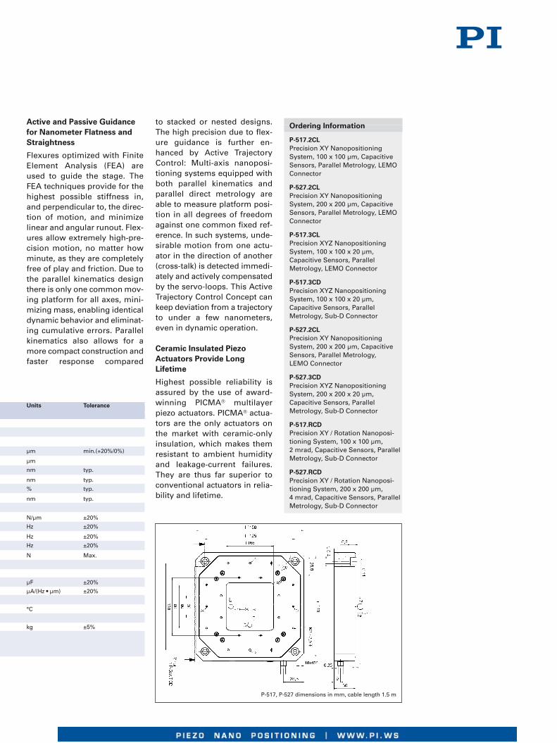
P-517, P-527 dimensions in mm, cable length 1.5 m

©P
hys
ikIn
stru
men
te(P
I)G
mb
H&
Co
.KG
2008
.Su
bje
ctto
chan
ge
wit
ho
ut
no
tice
.All
dat
aar
esu
per
sed
edb
yan
yn
ewre
leas
e.T
he
new
est
rele
ase
for
dat
ash
eets
isav
aila
ble
for
do
wn
load
atw
ww
.pi.w
s.C
at12
0EIn
spir
atio
ns2
009
08/1
0.18
P-733.2 · P-733.3 XY(Z) Piezo-Nanopositioning Stage
P-733 XY and XYZ piezo drivenstages are fast and highly accu-rate nanopositioning and scan-ning systems. They provide apositioning and scanningrange of 100 x 100 (x10) µmtogether with sub-nanometerresolution and are equippedwith parallel-metrology capaci-
tive position feedback for supe-rior multi-axis linearity andrepeatability. The guiding accu-racy minimizes runout to under10 nm over the whole travelrange. In addition, the high-speed Z-axis of the P-733.3CDcan actively compensate anyout-of-plane Z-axis deviationduring XY motion.
Fastest Multi-Axis Systems /Direct Drive, Low Profile andLarge Apertures
P-733.2DD / .3DD multi-axispiezo nanopositioning systemsare the fastest ultra-high-precision, open-frame stagesfor scanning microscopy. Theyprovide a positioning and scan-ning range of 30 x 30 (x10) µm.P-733 nanopositioning andscanning stages feature verylow profiles, as low as 20 mm(0.8 inch). The novel, high-stiff-ness direct drive gives the sys-tems resonant frequencies ashigh as 2.2 kHz (4 x that of
other comparable systems),enabling millisecond scanningrates with sub-nanometer reso-lution.
Parallel-Kinematics /Metrology for EnhancedResponsiveness
In a parallel kinematics multi-axis system, all actuators actdirectly on one moving plat-form. This means that all axesmove the same minimizedmass and can be designed withidentical dynamic properties.Multi-axis nanopositioningsystems equipped with bothparallel kinematics and paral-lel, direct metrology are able tomeasure platform position inall degrees of freedom againstone common fixed reference.In such systems, undesirablemotion from one actuator inthe direction of another (crosstalk) is detected immediatelyand actively compensated bythe servo-loops.
Capacitive Sensors forSubnanometer Resolution
PI's proprietary capacitive sen-sors measure position directlyand without physical contact.They are free of friction andhysteresis, a fact which, incombination with the position-ing resolution of well under 1nm, makes it possible toachieve very high levels of lin-earity. A further advantage ofdirect metrology with capaci-tive sensors is the high phasefidelity and the high bandwidthof up to 10 kHz. The closed-loop resolution is 0.3 nm forthe X and Y axes and 0.2 nmfor the optional Z-axis. Thedirect drive versions are ratedto 0.1 nm resolution for everyaxis.
Large Variety of Models for aBroad Range of Applications
For Z-axis scanning applica-tions, the P-733.ZCD (see
p. 2-42) version is availablewith a travel range of 100 µm.For ultra-high-vacuum applica-tions down to 10-9 hPa, nanopo-sitioning systems as well ascomprehensive accessories,such as suitable feedthroughs,are available.
� Travel Ranges to 100 x 100 µm in X,Y & to 10 µm in Z� Resolution to 0.1 nm with Capacitive Sensors� High-Speed Versions with Direct Drive� Vacuum and Non-Magnetic Versions� Parallel Kinematics for Better Multi-Axis Accuracy and
Dynamics� Parallel Metrology for Active Trajectory Control� Frictionless, High-Precision Flexure Guiding System� Clear Aperture 50 x 50 mm for Transmitted-Light Applications
Ordering Information
P-733.2DDHigh-Dynamics High-PrecisionXY Nanopositioning System,30 x 30 µm, Direct Drive, CapacitiveSensors, Parallel Metrology,Sub-D Connector
P-733.3DDHigh-Dynamics PrecisionXYZ Nanopositioning System,30 x 30 x 10 µm, Direct Drive,Capacitive Sensors, ParallelMetrology, Sub-D Connector
P-733.2CD* / P-733.2CL*High-Precision XY NanopositioningSystem, 100 x 100 µm, CapacitiveSensors, Parallel Metrology
P-733.3CD* / P-733.3CL*Precision XYZ NanopositioningSystem, 100 x 100 x 10 µm,Capacitive Sensors, ParallelMetrology
P-733.2VL* / P-733.2VD*High-Precision XY NanopositioningSystem, 100 x 100 µm, CapacitiveSensors, Parallel Metrology,Vacuum Compatible to 10-6 hPa
P-733.2UDHigh-Precision XY NanopositioningSystem, 100 x 100 µm, CapacitiveSensors, parallel metrology,Sub-D Connector, VacuumCompatible to 10-9 hPa
*.xxD with Sub-D Connector
*.xxL with LEMO Connector
Ask about custom designs
Application Examples
� Image processing /stablilization
� Scanning microscopy
� Surface inspection
� Metrology / interferometry
� Biotechnology
� Semiconductor testing
� Mask / wafer positioning
� Micromanipulation
� Nanopositioning with highflatness & straightness
High-Precision XY(Z) Scanner Family with Aperture
P -733.3 DD (left) and P -733.2 DD, high-speed, direct drive XY(Z)scanning stages are the fastest scanning stages with large aperture currently
available (2.2 kHz resonant frequency!). Both units feature a footprintof only 100 x 100 mm. CD for size comparison.
P-733.2UD non-magnetic XY scan-ning stage for UHV to 10-9 hPa
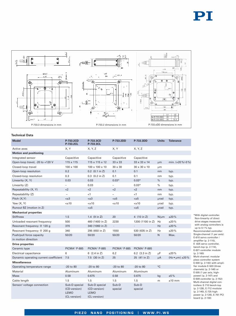
P-733.2 dimensions in mmP-733.3 dimensions in mm
Technical Data
Model P-733.2CD P-733.3CD P-733.2DD P-733.3DD Units ToleranceP-733.2CL P-733.3CL
Active axes X, Y X, Y, Z X, Y X, Y, Z
Motion and positioning
Integrated sensor Capacitive Capacitive Capacitive Capacitive
Open-loop travel, -20 to +120 V 115 x 115 115 x 115 x 12 33 x 33 33 x 33 x 14 µm min. (+20 %/-0 %)
Closed-loop travel 100 x 100 100 x 100 x 10 30 x 30 30 x 30 x 10 µm
Open-loop resolution 0.2 0.2 (0.1 in Z) 0.1 0.1 nm typ.
Closed-loop resolution 0.3 0.3 (0.2 in Z) 0.1 0.1 nm typ.
Linearity (X, Y) 0.03 0.03 0.03* 0.03* % typ.
Linearity (Z) – 0.03 – 0.03* % typ.
Repeatability (X, Y) <2 <2 <2 <2 nm typ.
Repeatability (Z) – <1 – <1 nm typ.
Pitch (X,Y) <±3 <±3 <±5 <±5 µrad typ.
Yaw (X, Y) <±10 <±10 <±10 <±10 µrad typ.
Runout θZ (motion in Z) <±5 <±5 µrad typ.
Mechanical properties
Stiffness 1.5 1.4 (9 in Z) 20 4 (10 in Z) N/µm ±20 %
Unloaded resonant frequency 500 460 (1400 in Z) 2230 1200 (1100 in Z) Hz ±20 %
Resonant frequency @ 120 g 370 340 (1060 in Z) - - Hz ±20 %
Resonant frequency @ 200 g 340 295 (650 in Z) 1550 530 (635 in Z) Hz ±20 %
Push/pull force capacity 50/20 50/20 50/20 50/20 N Max.
in motion direction
Drive properties
Ceramic type PICMA® P-885 PICMA® P-885 PICMA® P-885 PICMA® P-885
Electrical capacitance 6 6 (2.4 in Z) 6.2 6.2 (3.3 in Z) µF ±20 %
Dynamic operating current coefficient 7.5 7.5 (30 in Z) 25 25 (41 in Z) µA (Hz • µm) ±20 %
Miscellaneous
Operating temperature range -20 to 80 -20 to 80 -20 to 80 -20 to 80 °C
Material Aluminum Aluminum Aluminum Aluminum
Mass 0.58 0.675 0.58 0.675 kg ±5 %
Cable length 1.5 1.5 1.5 1.5 m ±10 mm
Sensor/ voltage connection Sub-D special Sub-D special Sub-D Sub-D(CD-version) (CD-version) special specialLEMO LEMO(CL-version) (CL-version)
*With digital controller.Non-linearity of directdrive stages measuredwith analog controllers isup to 0.1 % typ.
Recommended controller:Single-channel (1 per axis):E-610 servo controller /amplifier (p. 2-110),E -625 servo controller,bench-top (p. 2-114),E-621 controller module(p. 2-160)Multi-channel: modularpiezo controller systemE-500 (p. 2-142) with ampli-fier module E-503 (threechannels) (p. 2-146) orE-505 (1 per axis, high-power) (p. 2-147) andE-509 controller (p. 2-152)Multi-channel digital con-trollers: E-710 bench-top(p. 2-128), E-712 modular(p. 2-140), E-725 high-power (p. 2-126), E-761 PCIboard (p. 2-130)
P-733.xDD dimensions in mm
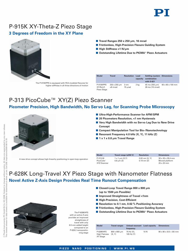
P-915K XY-Theta-Z Piezo Stage3 Degrees of Freedom in the XY Plane
� Travel Ranges 250 x 250 µm, 16 mrad� Frictionless, High-Precision Flexure Guiding System� High Stiffness >1 N/µm� Outstanding Lifetime Due to PICMA® Piezo Actuators
P-313 PicoCube™ XY(Z) Piezo ScannerPicometer Precision, High Bandwidth, No Servo Lag, for Scanning Probe Microscopy
� Ultra-High-Performance Scanner for AFM/SPM � 20 Picometers Resolution, <1 nm Hysteresis� Very High Bandwidth with no Servo Lag Due to New Drive
Concept� Compact Manipulation Tool for Bio-/Nanotechnology� Resonant Frequency 4.0 kHz (X, Y), 11 kHz (Z)� 1 x 1 x 0.8 µm Travel Range
P-628K Long-Travel XY Piezo Stage with Nanometer FlatnessNovel Active Z-Axis Design Provides Real Time Runout Compensation
� Closed-Loop Travel Range 800 x 800 µm (up to 1500 µm Possible)
� Improved Straightness of Travel <1nm� High-Precision, Cost-Efficient� Resolution to 0.1 nm, 0.02 % Positioning Accuracy� Frictionless, High-Precision Flexure Guiding System� Outstanding Lifetime Due to PICMA® Piezo Actuators
The P-915KPPS is equipped with FEA-modeled flexures forhigher stiffness in all three directions of motion
A new drive concept allows high-linearity positioning in open-loop operation
The P-628KHFS with an active Z-axis
provides an improvedstraightness of
travel with only 9.5 mm added height
compared to an P-628.2 nano positio-
ning stage
Model Travel Resolution Load Settling (system Dimensionscapacity combination
with E-621
P-915KPPS 250 x 250 µm 3 nm 2 kg 45 ms (250 µm) 60 x 60 x 100 mmXY-Rot-Z- ±8 mrad 15 µrad 28 ms (16 mrad)Piezo Stage
Model Travel range (±250 V) Resolution Dimensions
P-313.30 1 x 1 µm (X,Y) 0.02 nm (X, Y) 30 x 30 x 29.4 mmPicoCube™ 0.8 µm (Z) 0.14 nm (Z) Moved platform XYZ Scanner 20 x 20 mm
Model Travel ranges Unload resonant Load capacity Dimensionsfrequency
P-628KHFS 800 x 800 µm 75 Hz (X), 10 N 80 x 80 x (9.5 + 30) mmHigh Flatness (X, Y) 105 Hz (Y)XY Stage©
Ph
ysik
Inst
rum
ente
(P
I) G
mb
H &
Co
. KG
200
8. S
ub
ject
to
ch
ang
e w
ith
ou
t n
oti
ce. A
ll d
ata
are
sup
erse
ded
by
any
new
rel
ease
.T
he
new
est
rele
ase
for
dat
a sh
eets
is a
vaila
ble
fo
r d
ow
nlo
ad a
t w
ww
.pi.w
s. C
at12
0E In
spir
atio
ns2
009
08/1
0.18

USA (East) & CANADA USA (West) & MEXICO
PI (Physik Instrumente) L.P. PI (Physik Instrumente) L.P.16 Albert St. 5420 Trabuco Rd., Suite 100 Auburn, MA 01501 Irvine, CA 92620Tel: +1 (508) 832 3456 Tel: +1 (949) 679 9191Fax: +1 (508) 832 0506 Fax: +1 (949) 679 [email protected] [email protected] www.pi-usa.us
JAPAN
PI Japan Co., Ltd. PI Japan Co., Ltd.Akebono-cho 2-38-5 Hanahara Dai-ni Building, #703Tachikawa-shi 4-11-27 Nishinakajima,J-Tokyo 190 Yodogawa-ku, Osaka-shiTel: +81 (42) 526 7300 J-Osaka 532Fax: +81 (42) 526 7301 Tel: +81 (6) 6304 [email protected] Fax: +81 (6) 6304 5606www.pi-japan.jp [email protected]
www.pi-japan.jp
CHINA UK & IRELAND
Physik Instrumente PI (Physik Instrumente) Ltd.(PI Shanghai) Co., Ltd. Trent HouseBuilding No. 7-301 University Way,Longdong Avenue 3000 Cranfield Technology Park,201203 Shanghai, China Cranfield,Tel: +86 (21) 687 900 08 Bedford MK43 0ANFax: +86 (21) 687 900 98 Tel: +44 (1234) 756 [email protected] Fax: +44 (1234) 756 369www.pi-china.cn [email protected]
www.physikinstrumente.co.uk
ITALY
Physik Instrumente (PI) S.r.l.Via G. Marconi, 28I-20091 Bresso (MI)Tel: +39 (02) 665 011 01Fax: +39 (02) 873 859 [email protected]
FRANCE
PI France S.A.S244 bis, avenue Max Dormoy92120 MontrougeTel: +33 (1) 55 22 60 00 Fax: +33 (1) 41 48 56 62
GERMANY
Physik Instrumente (PI)GmbH & Co. KGAuf der Römerstr. 1D-76228 Karlsruhe/PalmbachTel: +49 (721) 4846-0 Fax: +49 (721) [email protected] · www.pi.ws
Program Overview
� Piezo Ceramic Actuators & Motors
� Piezo Nanopositioning Systems and Scanners
� Active Optics / Tip-Tilt Platforms
� Capacitive Nanometrology Sensors
� Piezo Electronics: Amplifiers and Controllers
� Hexapod 6-Axis Positioners / Robots
� Micropositioning Stages & Actuators
� Photonics Alignment Systems, Solutions forTelecommunications
� Motor Controllers
� Ultrasonic Linear Motors
Request or download the completePI Nanopositioning & Piezo ActuatorCatalog