xilinx ds031 virtex-ii platform fpgas: complete data sheet ... sheets/xilinx pdfs/virtex-ii... ·...
TRANSCRIPT

© 2000–2007 Xilinx, Inc. All rights reserved. XILINX, the Xilinx logo, the Brand Window, and other designated brands included herein are trademarks of Xilinx, Inc. All other trademarks are the property of their respective owners.
DS031 (v3.5) November 5, 2007 www.xilinx.comProduct Specification 1
Module 1: Introduction and Overview7 pages
• Summary of Features• General Description• Architecture• Device/Package Combinations and Maximum I/O• Ordering Examples
Module 2: Functional Description41 pages
• Detailed Description- Input/Output Blocks (IOBs)- Digitally Controlled Impedance (DCI)- Configurable Logic Blocks (CLBs)- 18-Kb Block SelectRAM™ Resources- 18-Bit x 18-Bit Multipliers- Global Clock Multiplexer Buffers- Digital Clock Manager (DCM)
• Routing• Creating a Design• Configuration
Module 3: DC and Switching Characteristics43 pages
• Electrical Characteristics• Performance Characteristics• Switching Characteristics• Pin-to-Pin Output Parameter Guidelines• Pin-to-Pin Input Parameter Guidelines• DCM Timing Parameters• Source-Synchronous Switching Characteristics
Module 4: Pinout Information226 pages
• Pin Definitions• Pinout Tables
- CS144/CSG144 Chip-Scale BGA Package- FG256/FGG256 Fine-Pitch BGA Package- FG456/FGG456 Fine-Pitch BGA Package- FG676/FGG676 Fine-Pitch BGA Package- BG575/BGG575 Standard BGA Package- BG728/BGG728 Standard BGA Package- FF896 Flip-Chip Fine-Pitch BGA Package- FF1152 Flip-Chip Fine-Pitch BGA Package- FF1517 Flip-Chip Fine-Pitch BGA Package- BF957Flip-Chip BGA Package
IMPORTANT NOTE: Page, figure, and table numbers begin at 1 for each module, and each module has its own RevisionHistory at the end. Use the PDF "Bookmarks" pane for easy navigation in this volume.
1Virtex-II Platform FPGAs:
Complete Data Sheet
DS031 (v3.5) November 5, 2007 Product Specification
R

© 2000–2007 Xilinx, Inc. All rights reserved. XILINX, the Xilinx logo, the Brand Window, and other designated brands included herein are trademarks of Xilinx, Inc. All other trademarks are the property of their respective owners.
DS031-1 (v3.5) November 5, 2007 www.xilinx.com Module 1 of 4Product Specification 1
Summary of Virtex-II™ Features• Industry First Platform FPGA Solution • IP-Immersion Architecture
- Densities from 40K to 8M system gates- 420 MHz internal clock speed (Advance Data)- 840+ Mb/s I/O (Advance Data)
• SelectRAM™ Memory Hierarchy- 3 Mb of dual-port RAM in 18 Kbit block SelectRAM
resources- Up to 1.5 Mb of distributed SelectRAM resources
• High-Performance Interfaces to External Memory- DRAM interfaces
· SDR / DDR SDRAM· Network FCRAM · Reduced Latency DRAM
- SRAM interfaces· SDR / DDR SRAM· QDR™ SRAM
- CAM interfaces• Arithmetic Functions
- Dedicated 18-bit x 18-bit multiplier blocks- Fast look-ahead carry logic chains
• Flexible Logic Resources- Up to 93,184 internal registers / latches with Clock
Enable- Up to 93,184 look-up tables (LUTs) or cascadable
16-bit shift registers- Wide multiplexers and wide-input function support- Horizontal cascade chain and sum-of-products
support- Internal 3-state bussing
• High-Performance Clock Management Circuitry- Up to 12 DCM (Digital Clock Manager) modules
· Precise clock de-skew· Flexible frequency synthesis· High-resolution phase shifting
- 16 global clock multiplexer buffers• Active Interconnect Technology
- Fourth generation segmented routing structure- Predictable, fast routing delay, independent of
fanout• SelectIO™-Ultra Technology
- Up to 1,108 user I/Os- 19 single-ended and six differential standards- Programmable sink current (2 mA to 24 mA) per I/O- Digitally Controlled Impedance (DCI) I/O: on-chip
termination resistors for single-ended I/O standards
- PCI-X compatible (133 MHz and 66 MHz) at 3.3V- PCI compliant (66 MHz and 33 MHz) at 3.3V- CardBus compliant (33 MHz) at 3.3V- Differential Signaling
· 840 Mb/s Low-Voltage Differential Signaling I/O (LVDS) with current mode drivers
· Bus LVDS I/O· Lightning Data Transport (LDT) I/O with current
driver buffers· Low-Voltage Positive Emitter-Coupled Logic
(LVPECL) I/O· Built-in DDR input and output registers
- Proprietary high-performance SelectLink Technology· High-bandwidth data path· Double Data Rate (DDR) link· Web-based HDL generation methodology
• Supported by Xilinx Foundation™ and Alliance Series™ Development Systems- Integrated VHDL and Verilog design flows- Compilation of 10M system gates designs- Internet Team Design (ITD) tool
• SRAM-Based In-System Configuration- Fast SelectMAP configuration- Triple Data Encryption Standard (DES) security
option (Bitstream Encryption)- IEEE 1532 support - Partial reconfiguration- Unlimited reprogrammability- Readback capability
• 0.15 µm 8-Layer Metal Process with 0.12 µm High-Speed Transistors
• 1.5V (VCCINT) Core Power Supply, Dedicated 3.3V VCCAUX Auxiliary and VCCO I/O Power Supplies
• IEEE 1149.1 Compatible Boundary-Scan Logic Support
• Flip-Chip and Wire-Bond Ball Grid Array (BGA) Packages in Three Standard Fine Pitches (0.80 mm, 1.00 mm, and 1.27 mm)
• Wire-Bond BGA Devices Available in Pb-Free Packaging (www.xilinx.com/pbfree)
• 100% Factory Tested
7Virtex-II Platform FPGAs:
Introduction and Overview
DS031-1 (v3.5) November 5, 2007 Product Specification
R

Virtex-II Platform FPGAs: Introduction and OverviewR
DS031-1 (v3.5) November 5, 2007 www.xilinx.com Module 1 of 4Product Specification 2
General DescriptionThe Virtex-II family is a platform FPGA developed for highperformance from low-density to high-density designs thatare based on IP cores and customized modules. The familydelivers complete solutions for telecommunication, wire-less, networking, video, and DSP applications, includingPCI, LVDS, and DDR interfaces.
The leading-edge 0.15 µm / 0.12 µm CMOS 8-layer metalprocess and the Virtex-II architecture are optimized for highspeed with low power consumption. Combining a wide vari-ety of flexible features and a large range of densities up to10 million system gates, the Virtex-II family enhances pro-grammable logic design capabilities and is a powerful alter-native to mask-programmed gates arrays. As shown inTable 1, the Virtex-II family comprises 11 members, rangingfrom 40K to 8M system gates.
PackagingOfferings include ball grid array (BGA) packages with0.80 mm, 1.00 mm, and 1.27 mm pitches. In addition to tra-ditional wire-bond interconnects, flip-chip interconnect isused in some of the BGA offerings. The use of flip-chipinterconnect offers more I/Os than is possible in wire-bondversions of the similar packages. Flip-chip constructionoffers the combination of high pin count with high thermalcapacity.
Wire-bond packages CS, FG, and BG are optionally avail-abe in Pb-free versions CSG, FGG, and BGG. See Virtex-IIOrdering Examples, page 6.
Table 2 shows the maximum number of user I/Os available.The Virtex-II device/package combination table (Table 6 atthe end of this section) details the maximum number of I/Osfor each device and package using wire-bond or flip-chiptechnology.
Table 1: Virtex-II Field-Programmable Gate Array Family Members
DeviceSystem Gates
CLB (1 CLB = 4 slices = Max 128 bits)
Multiplier Blocks
SelectRAM Blocks
DCMsMax I/O Pads(1)
Array Row x Col. Slices
Maximum Distributed RAM Kbits
18 Kbit Blocks
Max RAM (Kbits)
XC2V40 40K 8 x 8 256 8 4 4 72 4 88
XC2V80 80K 16 x 8 512 16 8 8 144 4 120
XC2V250 250K 24 x 16 1,536 48 24 24 432 8 200
XC2V500 500K 32 x 24 3,072 96 32 32 576 8 264
XC2V1000 1M 40 x 32 5,120 160 40 40 720 8 432
XC2V1500 1.5M 48 x 40 7,680 240 48 48 864 8 528
XC2V2000 2M 56 x 48 10,752 336 56 56 1,008 8 624
XC2V3000 3M 64 x 56 14,336 448 96 96 1,728 12 720
XC2V4000 4M 80 x 72 23,040 720 120 120 2,160 12 912
XC2V6000 6M 96 x 88 33,792 1,056 144 144 2,592 12 1,104
XC2V8000 8M 112 x 104 46,592 1,456 168 168 3,024 12 1,108
Notes: 1. See details in Table 2, “Maximum Number of User I/O Pads”.
Table 2: Maximum Number of User I/O Pads
Device Wire-Bond Flip-Chip
XC2V40 88 -
XC2V80 120 -
XC2V250 200 -
XC2V500 264 -
XC2V1000 328 432
XC2V1500 392 528
XC2V2000 - 624
XC2V3000 516 720
XC2V4000 - 912
XC2V6000 - 1,104
XC2V8000 - 1,108

Virtex-II Platform FPGAs: Introduction and OverviewR
DS031-1 (v3.5) November 5, 2007 www.xilinx.com Module 1 of 4Product Specification 3
Architecture
Virtex-II Array OverviewVirtex-II devices are user-programmable gate arrays with various configurable elements. The Virtex-II architecture is optimized for high-density and high-performance logic designs. As shown in Figure 1, the programmable device is comprised of input/output blocks (IOBs) and internal configurable logic blocks (CLBs).
Programmable I/O blocks provide the interface between package pins and the internal configurable logic. Most popular and leading-edge I/O standards are supported by the programmable IOBs.
The internal configurable logic includes four major elementsorganized in a regular array.
• Configurable Logic Blocks (CLBs) provide functional elements for combinatorial and synchronous logic, including basic storage elements. BUFTs (3-state buffers) associated with each CLB element drive dedicated segmentable horizontal routing resources.
• Block SelectRAM memory modules provide large 18 Kbit storage elements of dual-port RAM.
• Multiplier blocks are 18-bit x 18-bit dedicated multipliers.
• DCM (Digital Clock Manager) blocks provide self-calibrating, fully digital solutions for clock distribution delay compensation, clock multiplication and division, coarse- and fine-grained clock phase shifting.
A new generation of programmable routing resources calledActive Interconnect Technology interconnects all of theseelements. The general routing matrix (GRM) is an array ofrouting switches. Each programmable element is tied to aswitch matrix, allowing multiple connections to the generalrouting matrix. The overall programmable interconnection ishierarchical and designed to support high-speed designs.
All programmable elements, including the routingresources, are controlled by values stored in static memorycells. These values are loaded in the memory cells during
configuration and can be reloaded to change the functionsof the programmable elements.
Virtex-II FeaturesThis section briefly describes Virtex-II features.
Input/Output Blocks (IOBs)IOBs are programmable and can be categorized as follows:
• Input block with an optional single-data-rate or double-data-rate (DDR) register
• Output block with an optional single-data-rate or DDR register, and an optional 3-state buffer, to be driven directly or through a single or DDR register
• Bidirectional block (any combination of input and output configurations)
These registers are either edge-triggered D-type flip-flopsor level-sensitive latches.
IOBs support the following single-ended I/O standards:
• LVTTL, LVCMOS (3.3V, 2.5V, 1.8V, and 1.5V)
• PCI-X compatible (133 MHz and 66 MHz) at 3.3V
• PCI compliant (66 MHz and 33 MHz) at 3.3V
• CardBus compliant (33 MHz) at 3.3V
• GTL and GTLP
Figure 1: Virtex-II Architecture Overview
Global Clock Mux
DCM DCM IOB
CLBProgrammable I/Os
Block SelectRAM Multiplier
Configurable Logic
DS031_28_100900

Virtex-II Platform FPGAs: Introduction and OverviewR
DS031-1 (v3.5) November 5, 2007 www.xilinx.com Module 1 of 4Product Specification 4
• HSTL (Class I, II, III, and IV)
• SSTL (3.3V and 2.5V, Class I and II)
• AGP-2X
The digitally controlled impedance (DCI) I/O feature auto-matically provides on-chip termination for each I/O element.
The IOB elements also support the following differential sig-naling I/O standards:
• LVDS
• BLVDS (Bus LVDS)
• ULVDS
• LDT
• LVPECL
Two adjacent pads are used for each differential pair. Two orfour IOB blocks connect to one switch matrix to access therouting resources.
Configurable Logic Blocks (CLBs)
CLB resources include four slices and two 3-state buffers.Each slice is equivalent and contains:
• Two function generators (F & G)
• Two storage elements
• Arithmetic logic gates
• Large multiplexers
• Wide function capability
• Fast carry look-ahead chain
• Horizontal cascade chain (OR gate)
The function generators F & G are configurable as 4-inputlook-up tables (LUTs), as 16-bit shift registers, or as 16-bitdistributed SelectRAM memory.
In addition, the two storage elements are either edge-trig-gered D-type flip-flops or level-sensitive latches.
Each CLB has internal fast interconnect and connects to aswitch matrix to access general routing resources.
Block SelectRAM Memory
The block SelectRAM memory resources are 18 Kb ofdual-port RAM, programmable from 16K x 1 bit to 512 x 36bits, in various depth and width configurations. Each port istotally synchronous and independent, offering three"read-during-write" modes. Block SelectRAM memory iscascadable to implement large embedded storage blocks.Supported memory configurations for dual-port and sin-gle-port modes are shown in Table 3.
A multiplier block is associated with each SelectRAM mem-ory block. The multiplier block is a dedicated 18 x 18-bitmultiplier and is optimized for operations based on the blockSelectRAM content on one port. The 18 x 18 multiplier canbe used independently of the block SelectRAM resource.Read/multiply/accumulate operations and DSP filter struc-tures are extremely efficient.
Both the SelectRAM memory and the multiplier resourceare connected to four switch matrices to access the generalrouting resources.
Global ClockingThe DCM and global clock multiplexer buffers provide acomplete solution for designing high-speed clockingschemes.
Up to 12 DCM blocks are available. To generate de-skewedinternal or external clocks, each DCM can be used to elimi-nate clock distribution delay. The DCM also provides 90-,180-, and 270-degree phase-shifted versions of its outputclocks. Fine-grained phase shifting offers high-resolutionphase adjustments in increments of 1/256 of the clockperiod. Very flexible frequency synthesis provides a clockoutput frequency equal to any M/D ratio of the input clockfrequency, where M and D are two integers. For the exacttiming parameters, see Virtex-II Electrical Characteristics.
Virtex-II devices have 16 global clock MUX buffers, with upto eight clock nets per quadrant. Each global clock MUXbuffer can select one of the two clock inputs and switchglitch-free from one clock to the other. Each DCM block isable to drive up to four of the 16 global clock MUX buffers.
Routing ResourcesThe IOB, CLB, block SelectRAM, multiplier, and DCM ele-ments all use the same interconnect scheme and the sameaccess to the global routing matrix. Timing models areshared, greatly improving the predictability of the perfor-mance of high-speed designs.
There are a total of 16 global clock lines, with eight availableper quadrant. In addition, 24 vertical and horizontal longlines per row or column as well as massive secondary andlocal routing resources provide fast interconnect. Virtex-IIbuffered interconnects are relatively unaffected by netfanout and the interconnect layout is designed to minimizecrosstalk.
Horizontal and vertical routing resources for each row orcolumn include:
• 24 long lines• 120 hex lines• 40 double lines• 16 direct connect lines (total in all four directions)
Table 3: Dual-Port And Single-Port Configurations
16K x 1 bit 2K x 9 bits
8K x 2 bits 1K x 18 bits
4K x 4 bits 512 x 36 bits

Virtex-II Platform FPGAs: Introduction and OverviewR
DS031-1 (v3.5) November 5, 2007 www.xilinx.com Module 1 of 4Product Specification 5
Boundary Scan
Boundary scan instructions and associated data registerssupport a standard methodology for accessing and config-uring Virtex-II devices that complies with IEEE standards1149.1 — 1993 and 1532. A system mode and a test modeare implemented. In system mode, a Virtex-II device per-forms its intended mission even while executing non-testboundary-scan instructions. In test mode, boundary-scantest instructions control the I/O pins for testing purposes.The Virtex-II Test Access Port (TAP) supports BYPASS,PRELOAD, SAMPLE, IDCODE, and USERCODE non-testinstructions. The EXTEST, INTEST, and HIGHZ test instruc-tions are also supported.
ConfigurationVirtex-II devices are configured by loading data into internalconfiguration memory, using the following five modes:
• Slave-serial mode• Master-serial mode• Slave SelectMAP mode• Master SelectMAP mode• Boundary-Scan mode (IEEE 1532)
A Data Encryption Standard (DES) decryptor is availableon-chip to secure the bitstreams. One or two triple-DES keysets can be used to optionally encrypt the configurationinformation.
Readback and Integrated Logic AnalyzerConfiguration data stored in Virtex-II configuration memorycan be read back for verification. Along with the configura-tion data, the contents of all flip-flops/latches, distributed
SelectRAM, and block SelectRAM memory resources canbe read back. This capability is useful for real-time debug-ging.
The Integrated Logic Analyzer (ILA) core and software pro-vides a complete solution for accessing and verifyingVirtex-II devices.
Virtex-II Device/Package Combinations and Maximum I/OWire-bond and flip-chip packages are available. Table 4 andTable 5 show the maximum possible number of user I/Os inwire-bond and flip-chip packages, respectively. Table 6shows the number of available user I/Os for all device/pack-age combinations.
• CS denotes wire-bond chip-scale ball grid array (BGA) (0.80 mm pitch).
• CSG denotes Pb-free wire-bond chip-scale ball grid array (BGA) (0.80 mm pitch).
• FG denotes wire-bond fine-pitch BGA (1.00 mm pitch). • FGG denotes Pb-free wire-bond fine-pitch BGA (1.00
mm pitch). • BG denotes standard BGA (1.27 mm pitch).• BGG denotes Pb-free standard BGA (1.27 mm pitch).• FF denotes flip-chip fine-pitch BGA (1.00 mm pitch).• BF denotes flip-chip BGA (1.27 mm pitch).
The number of I/Os per package include all user I/Os exceptthe 15 control pins (CCLK, DONE, M0, M1, M2, PROG_B,PWRDWN_B, TCK, TDI, TDO, TMS, HSWAP_EN, DXN,DXP, and RSVD) and VBATT.
Table 4: Wire-Bond Packages Information
Package(1)CS144/CSG144
FG256/FGG256
FG456/FGG456
FG676/FGG676
BG575/BGG575
BG728/BGG728
Pitch (mm) 0.80 1.00 1.00 1.00 1.27 1.27
Size (mm) 12 x 12 17 x 17 23 x 23 27 x 27 31 x 31 35 x 35
I/Os 92 172 324 484 408 516
Notes: 1. Wire-bond packages include FGGnnn Pb-free versions. See Virtex-II Ordering Examples (Module 1).
Table 5: Flip-Chip Packages Information
Package FF896 FF1152 FF1517 BF957
Pitch (mm) 1.00 1.00 1.00 1.27
Size (mm) 31 x 31 35 x 35 40 x 40 40 x 40
I/Os 624 824 1,108 684

Virtex-II Platform FPGAs: Introduction and OverviewR
DS031-1 (v3.5) November 5, 2007 www.xilinx.com Module 1 of 4Product Specification 6
Virtex-II Ordering Examples
Table 6: Virtex-II Device/Package Combinations and Maximum Number of Available I/Os (Advance Information)
Package(1,2)
Available I/Os
XC2V40
XC2V80
XC2V250
XC2V500
XC2V1000
XC2V1500
XC2V2000
XC2V3000
XC2V4000
XC2V6000
XC2V8000
CS144/CSG144 88 92 92 - - - - - - - -
FG256/FGG256 88 120 172 172 172 - - - - - -
FG456/FGG456 - - 200 264 324 - - - - - -
FG676/FGG676 - - - - - 392 456 484 - - -
FF896 - - - - 432 528 624 - - - -
FF1152 - - - - - - - 720 824 824 824
FF1517 - - - - - - - - 912 1,104 1,108
BG575/BGG575 - - - - 328 392 408 - - - -
BG728/BGG728 - - - - - - - 516 - - -
BF957 - - - - - - 624 684 684 684 -
Notes: 1. All devices in a particular package are pinout (footprint) compatible. In addition, the FG456/FGG456 and FG676/FGG676 packages
are compatible, as are the FF896 and FF1152 packages.2. Wire-bond packages CS144, FG256, FG456, FG676, BG575, and BG728 are also available in Pb-free versions CSG144, FGG256, FGG456,
FGG676, BGG575, and BGG728. See Virtex-II Ordering Examples for details on how to order.
Figure 2: Virtex-II Ordering Example. Regular Package
Example: XC2V1000-5FG456C
Device Type Temperature RangeC = Commercial (Tj = 0˚C to +85˚C)I = Industrial (Tj = –40˚C to +100˚C)
Number of Pins
Package Type
Speed Grade(-4, -5, -6)
DS031_35_033001
Figure 3: Virtex-II Ordering Example. Pb-Free Package
Example: XC2V3000-6BGG728C
Device Type Temperature RangeC = Commercial (Tj = 0˚C to +85˚C)I = Industrial (Tj = –40˚C to +100˚C)Number of PinsPb-Free PackagePackage Type
Speed Grade(-4, -5, -6)
DS031_35a_061804

Virtex-II Platform FPGAs: Introduction and OverviewR
DS031-1 (v3.5) November 5, 2007 www.xilinx.com Module 1 of 4Product Specification 7
Revision HistoryThis section records the change history for this module of the data sheet.
Notice of DisclaimerTHE XILINX HARDWARE FPGA AND CPLD DEVICES REFERRED TO HEREIN (“PRODUCTS”) ARE SUBJECT TO THE TERMS ANDCONDITIONS OF THE XILINX LIMITED WARRANTY WHICH CAN BE VIEWED AT http://www.xilinx.com/warranty.htm. THIS LIMITEDWARRANTY DOES NOT EXTEND TO ANY USE OF PRODUCTS IN AN APPLICATION OR ENVIRONMENT THAT IS NOT WITHIN THESPECIFICATIONS STATED IN THE XILINX DATA SHEET. ALL SPECIFICATIONS ARE SUBJECT TO CHANGE WITHOUT NOTICE.PRODUCTS ARE NOT DESIGNED OR INTENDED TO BE FAIL-SAFE OR FOR USE IN ANY APPLICATION REQUIRING FAIL-SAFEPERFORMANCE, SUCH AS LIFE-SUPPORT OR SAFETY DEVICES OR SYSTEMS, OR ANY OTHER APPLICATION THAT INVOKESTHE POTENTIAL RISKS OF DEATH, PERSONAL INJURY, OR PROPERTY OR ENVIRONMENTAL DAMAGE (“CRITICALAPPLICATIONS”). USE OF PRODUCTS IN CRITICAL APPLICATIONS IS AT THE SOLE RISK OF CUSTOMER, SUBJECT TOAPPLICABLE LAWS AND REGULATIONS.
Virtex-II Data SheetThe Virtex-II Data Sheet contains the following modules:
• Virtex-II Platform FPGAs: Introduction and Overview (Module 1)
• Virtex-II Platform FPGAs: Functional Description (Module 2)
• Virtex-II Platform FPGAs: DC and Switching Characteristics (Module 3)
• Virtex-II Platform FPGAs: Pinout Information (Module 4)
Date Version Revision
11/07/00 1.0 Early access draft.
12/06/00 1.1 Initial release.
01/15/01 1.2 Added values to the tables in the Virtex-II Performance Characteristics and Virtex-II Switching Characteristics sections.
01/25/01 1.3 The data sheet was divided into four modules (per the current style standard).
04/02/01 1.5 Skipped v1.4 to sync up modules. Reverted to traditional double-column format.
07/30/01 1.6 Made minor changes to items listed under Summary of Virtex-II™ Features.
10/02/01 1.7 Minor edits.
07/16/02 1.8 Updated Virtex-II Device/Package Combinations shown in Table 6.
09/26/02 1.9 Updated Table 2 and Table 6 to reflect supported Virtex-II Device/Package Combinations.
08/01/03 2.0 All Virtex-II devices and speed grades now Production. See Table 13, Module 3.
03/29/04 2.0.1 Recompiled for backward compatibility with Acrobat 4 and above. No content changes.
06/24/04 3.3 Added references to available Pb-free wire-bond packages. (Revision number advanced to level of complete data sheet.)
03/01/05 3.4 No changes in Module 1 for this revision.
11/05/07 3.5 Updated copyright notice and legal disclaimer.

© 2000–2007 Xilinx, Inc. All rights reserved. XILINX, the Xilinx logo, the Brand Window, and other designated brands included herein are trademarks of Xilinx, Inc. All other trademarks are the property of their respective owners.
DS031-2 (v3.5) November 5, 2007 www.xilinx.com Module 2 of 4Product Specification 1
Detailed Description
Input/Output Blocks (IOBs)Virtex-II™ I/O blocks (IOBs) are provided in groups of two orfour on the perimeter of each device. Each IOB can be usedas input and/or output for single-ended I/Os. Two IOBs canbe used as a differential pair. A differential pair is alwaysconnected to the same switch matrix, as shown in Figure 1.
IOB blocks are designed for high performances I/Os, sup-porting 19 single-ended standards, as well as differentialsignaling with LVDS, LDT, Bus LVDS, and LVPECL.
Note: Differential I/Os must use the same clock.
Supported I/O StandardsVirtex-II IOB blocks feature SelectI/O-Ultra inputs and out-puts that support a wide variety of I/O signaling standards.In addition to the internal supply voltage (VCCINT = 1.5V),output driver supply voltage (VCCO) is dependent on the I/Ostandard (see Table 1 and Table 2). An auxiliary supply volt-age (VCCAUX = 3.3 V) is required, regardless of the I/Ostandard used. For exact supply voltage absolute maximumratings, see DC Input and Output Levels in Module 3.
All of the user IOBs have fixed-clamp diodes to VCCO and toground. As outputs, these IOBs are not compatible or com-pliant with 5V I/O standards. As inputs, these IOBs are notnormally 5V tolerant, but can be used with 5V I/O standardswhen external current-limiting resistors are used. For moredetails, see the “5V Tolerant I/Os“ Tech Topic at www.xil-inx.com.
Table 3 lists supported I/O standards with Digitally Con-trolled Impedance. See Digitally Controlled Impedance(DCI), page 8.
40 Virtex-II Platform FPGAs:
Functional Description
DS031-2 (v3.5) November 5, 2007 Product Specification
R
Figure 1: Virtex-II Input/Output Tile
IOBPAD4
IOBPAD3
Differential Pair
IOBPAD2
IOBPAD1
Differential Pair
SwitchMatrix
DS031_30_101600
Table 1: Supported Single-Ended I/O Standards
IOSTANDARD Attribute
OutputVCCO
InputVCCO
InputVREF
Board Termination Voltage (VTT)
LVTTL 3.3 3.3 N/R(3) N/R
LVCMOS33 3.3 3.3 N/R N/R
LVCMOS25 2.5 2.5 N/R N/R
LVCMOS18 1.8 1.8 N/R N/R
LVCMOS15 1.5 1.5 N/R N/R
PCI33_3 3.3 3.3 N/R N/R
PCI66_3 3.3 3.3 N/R N/R
PCI-X 3.3 3.3 N/R N/R
GTL Note (1) Note (1) 0.8 1.2
GTLP Note (1) Note (1) 1.0 1.5
HSTL_I 1.5 N/R 0.75 0.75
HSTL_II 1.5 N/R 0.75 0.75
HSTL_III 1.5 N/R 0.9 1.5
HSTL_IV 1.5 N/R 0.9 1.5
HSTL_I_18 1.8 N/R 0.9 0.9
HSTL_II_18 1.8 N/R 0.9 0.9
HSTL_III _18 1.8 N/R 1.1 1.8
HSTL_IV_18 1.8 N/R 1.1 1.8
SSTL18_I(2) 1.8 N/R 0.9 0.9
SSTL18_II 1.8 N/R 0.9 0.9
SSTL2_I 2.5 N/R 1.25 1.25
SSTL2_II 2.5 N/R 1.25 1.25
SSTL3_I 3.3 N/R 1.5 1.5
SSTL3_II 3.3 N/R 1.5 1.5
AGP-2X/AGP 3.3 N/R 1.32 N/R
Notes: 1. VCCO of GTL or GTLP should not be lower than the termination
voltage or the voltage seen at the I/O pad. Example: If the pin High level is 1.5V, connect VCCO to 1.5V.
2. SSTL18_I is not a JEDEC-supported standard.3. N/R = no requirement.

Virtex-II Platform FPGAs: Functional DescriptionR
DS031-2 (v3.5) November 5, 2007 www.xilinx.com Module 2 of 4Product Specification 2
Logic Resources
IOB blocks include six storage elements, as shown inFigure 2.
Each storage element can be configured either as anedge-triggered D-type flip-flop or as a level-sensitive latch.On the input, output, and 3-state path, one or two DDR reg-isters can be used.
Double data rate is directly accomplished by the two regis-ters on each path, clocked by the rising edges (or fallingedges) from two different clock nets. The two clock signalsare generated by the DCM and must be 180 degrees out ofphase, as shown in Figure 3. There are two input, output,and 3-state data signals, each being alternately clocked out.
Table 2: Supported Differential Signal I/O Standards
I/O StandardOutputVCCO
Input VCCO
InputVREF
OutputVOD
LVPECL_33 3.3 N/R(1) N/R 0.490 - 1.220
LDT_25 2.5 N/R N/R 0.500 - 0.700
LVDS_33 3.3 N/R N/R 0.250 - 0.400
LVDS_25 2.5 N/R N/R 0.250 - 0.400
LVDSEXT_33 3.3 N/R N/R 0.440 - 0.820
LVDSEXT_25 2.5 N/R N/R 0.440 - 0.820
BLVDS_25 2.5 N/R N/R 0.250 - 0.450
ULVDS_25 2.5 N/R N/R 0.500 - 0.700
Notes: 1. N/R = no requirement.
Table 3: Supported DCI I/O Standards
I/OStandard
OutputVCCO
InputVCCO
InputVREF
TerminationType
LVDCI_33(1) 3.3 3.3 N/R(4) Series
LVDCI_DV2_33(1) 3.3 3.3 N/R Series
LVDCI_25(1) 2.5 2.5 N/R Series
LVDCI_DV2_25(1) 2.5 2.5 N/R Series
LVDCI_18(1) 1.8 1.8 N/R Series
LVDCI_DV2_18(1) 1.8 1.8 N/R Series
LVDCI_15(1) 1.5 1.5 N/R Series
LVDCI_DV2_15(1) 1.5 1.5 N/R Series
GTL_DCI 1.2 1.2 0.8 Single
GTLP_DCI 1.5 1.5 1.0 Single
HSTL_I_DCI 1.5 1.5 0.75 Split
HSTL_II_DCI 1.5 1.5 0.75 Split
HSTL_III_DCI 1.5 1.5 0.9 Single
HSTL_IV_DCI 1.5 1.5 0.9 Single
HSTL_I_DCI_18 1.8 1.8 0.9 Split
HSTL_II_DCI_18 1.8 1.8 0.9 Split
HSTL_III_DCI_18 1.8 1.8 1.1 Single
HSTL_IV_DCI_18 1.8 1.8 1.1 Single
SSTL18_I_DCI(3) 1.8 1.8 0.9 Split
SSTL18_II_DCI 1.8 1.8 0.9 Split
SSTL2_I_DCI(2) 2.5 2.5 1.25 Split
SSTL2_II_DCI(2) 2.5 2.5 1.25 Split
SSTL3_I_DCI(2) 3.3 3.3 1.5 Split
SSTL3_II_DCI(2) 3.3 3.3 1.5 Split
LVDS_25_DCI 2.5 2.5 N/R Split
LVDSEXT_25_DCI 2.5 2.5 N/R Split
Notes: 1. LVDCI_XX and LVDCI_DV2_XX are LVCMOS controlled
impedance buffers, matching the reference resistors or half of the reference resistors.
2. These are SSTL compatible.3. SSTL18_I is not a JEDEC-supported standard.4. N/R = no requirement.
Figure 2: Virtex-II IOB Block
Reg
OCK1
Reg
OCK2
Reg
ICK1
Reg
ICK2
DDR muxInput
PAD
3-State
Reg
OCK1
Reg
OCK2
DDR mux
Output
IOB
DS031_29_100900

Virtex-II Platform FPGAs: Functional DescriptionR
DS031-2 (v3.5) November 5, 2007 www.xilinx.com Module 2 of 4Product Specification 3
The DDR mechanism shown in Figure 3 can be used to mir-ror a copy of the clock on the output. This is useful for prop-agating a clock along the data that has an identical delay. Itis also useful for multiple clock generation, where there is aunique clock driver for every clock load. Virtex-II devicescan produce many copies of a clock with very little skew.
Each group of two registers has a clock enable signal (ICEfor the input registers, OCE for the output registers, andTCE for the 3-state registers). The clock enable signals areactive High by default. If left unconnected, the clock enablefor that storage element defaults to the active state.
Each IOB block has common synchronous or asynchronousset and reset (SR and REV signals).
SR forces the storage element into the state specified by theSRHIGH or SRLOW attribute. SRHIGH forces a logic “1”.SRLOW forces a logic “0”. When SR is used, a second input(REV) forces the storage element into the opposite state. Thereset condition predominates over the set condition. The ini-tial state after configuration or global initialization state isdefined by a separate INIT0 and INIT1 attribute. By default,the SRLOW attribute forces INIT0, and the SRHIGH attributeforces INIT1.
For each storage element, the SRHIGH, SRLOW, INIT0,and INIT1 attributes are independent. Synchronous orasynchronous set / reset is consistent in an IOB block.
All the control signals have independent polarity. Anyinverter placed on a control input is automatically absorbed.
Each register or latch (independent of all other registers orlatches) (see Figure 4) can be configured as follows:
• No set or reset• Synchronous set• Synchronous reset• Synchronous set and reset• Asynchronous set (preset)• Asynchronous reset (clear)• Asynchronous set and reset (preset and clear)
The synchronous reset overrides a set, and an asynchro-nous clear overrides a preset.
Figure 3: Double Data Rate Registers
D1
CLK1
DDR MUX
Q1
FDDR
D2
CLK2
(50/50 duty cycle clock)
CLOCK
Q Q
Q2
D1
CLK1
DDR MUX
DCM
Q1
FDDR
D2
CLK2
Q2
180° 0°
DS031_26_100900

Virtex-II Platform FPGAs: Functional DescriptionR
DS031-2 (v3.5) November 5, 2007 www.xilinx.com Module 2 of 4Product Specification 4
Input/Output Individual OptionsEach device pad has optional pull-up and pull-down in allSelectI/O-Ultra configurations. Each device pad hasoptional weak-keeper in LVTTL, LVCMOS, and PCISelectI/O-Ultra configurations, as illustrated in Figure 5.Values of the optional pull-up and pull-down resistors are inthe range 10 - 60 KΩ, which is the specification for VCCOwhen operating at 3.3V (from 3.0 to 3.6V only). The clampdiode is always present, even when power is not.
The optional weak-keeper circuit is connected to each userI/O pad. When selected, the circuit monitors the voltage onthe pad and weakly drives the pin High or Low. If the pin isconnected to a multiple-source signal, the weak-keeperholds the signal in its last state if all drivers are disabled.Maintaining a valid logic level in this way eliminates buschatter. An enabled pull-up or pull-down overrides theweak-keeper circuit.
LVTTL sinks and sources current up to 24 mA. The currentis programmable for LVTTL and LVCMOS SelectI/O-Ultrastandards (see Table 4). Drive-strength and slew-rate con-trols for each output driver, minimize bus transients. ForLVDCI and LVDCI_DV2 standards, drive strength andslew-rate controls are not available.
Figure 4: Register / Latch Configuration in an IOB Block
FFLATCH
SR REV
D1 Q1
CE
CK1
FFLATCH
SR REV
D2
FF1
FF2DDR MUX
Q2
CECK2
REV
SR
(O/T) CLK1
(OQ or TQ)
(O/T) CE
(O/T) 1
(O/T) CLK2
(O/T) 2
Attribute INIT1INIT0SRHIGHSRLOW
Attribute INIT1INIT0SRHIGHSRLOW
Reset TypeSYNCASYNC
DS031_25_110300
Sharedby all
registers
Figure 5: LVTTL, LVCMOS or PCI SelectI/O-Ultra Standards
VCCO
VCCO
VCCO
WeakKeeper
ProgramDelay
OBUF
IBUF
ProgramCurrent
ClampDiode
PAD
VCCAUX = 3.3V
DS031_23_022205
VCCINT = 1.5V
10KΩ – 60KΩ
10KΩ – 60KΩ

Virtex-II Platform FPGAs: Functional DescriptionR
DS031-2 (v3.5) November 5, 2007 www.xilinx.com Module 2 of 4Product Specification 5
Figure 6 shows the SSTL2, SSTL3, and HSTL configura-tions. HSTL can sink current up to 48 mA. (HSTL IV)
All pads are protected against damage from electrostaticdischarge (ESD) and from over-voltage transients. Virtex-IIuses two memory cells to control the configuration of an I/Oas an input. This is to reduce the probability of an I/O con-figured as an input from flipping to an output when sub-jected to a single event upset (SEU) in space applications.
Prior to configuration, all outputs not involved in configura-tion are forced into their high-impedance state. Thepull-down resistors and the weak-keeper circuits are inac-tive. The dedicated pin HSWAP_EN controls the pull-upresistors prior to configuration. By default, HSWAP_EN isset high, which disables the pull-up resistors on user I/Opins. When HSWAP_EN is set low, the pull-up resistors areactivated on user I/O pins.
All Virtex-II IOBs support IEEE 1149.1 compatible Bound-ary-Scan testing.
Input PathThe Virtex-II IOB input path routes input signals directly tointernal logic and / or through an optional input flip-flop orlatch, or through the DDR input registers. An optional delayelement at the D-input of the storage element eliminatespad-to-pad hold time. The delay is matched to the internalclock-distribution delay of the Virtex-II device, and whenused, assures that the pad-to-pad hold time is zero.
Each input buffer can be configured to conform to any of thelow-voltage signaling standards supported. In some ofthese standards the input buffer utilizes a user-suppliedthreshold voltage, VREF. The need to supply VREF imposesconstraints on which standards can be used in the samebank. See I/O banking description.
Output PathThe output path includes a 3-state output buffer that drivesthe output signal onto the pad. The output and / or the3-state signal can be routed to the buffer directly from theinternal logic or through an output / 3-state flip-flop or latch,or through the DDR output / 3-state registers.
Each output driver can be individually programmed for awide range of low-voltage signaling standards. In most sig-naling standards, the output High voltage depends on anexternally supplied VCCO voltage. The need to supply VCCOimposes constraints on which standards can be used in thesame bank. See I/O banking description.
I/O Banking
Some of the I/O standards described above require VCCOand VREF voltages. These voltages are externally suppliedand connected to device pins that serve groups of IOBblocks, called banks. Consequently, restrictions exist aboutwhich I/O standards can be combined within a given bank.
Eight I/O banks result from dividing each edge of the FPGAinto two banks, as shown in Figure 7 and Figure 8. Eachbank has multiple VCCO pins, all of which must be con-nected to the same voltage. This voltage is determined bythe output standards in use.
Table 4: LVTTL and LVCMOS Programmable Currents (Sink and Source)
SelectI/O-Ultra Programmable Current (Worst-Case Guaranteed Minimum)
LVTTL 2 mA 4 mA 6 mA 8 mA 12 mA 16 mA 24 mA
LVCMOS33 2 mA 4 mA 6 mA 8 mA 12 mA 16 mA 24 mA
LVCMOS25 2 mA 4 mA 6 mA 8 mA 12 mA 16 mA 24 mA
LVCMOS18 2 mA 4 mA 6 mA 8 mA 12 mA 16 mA n/a
LVCMOS15 2 mA 4 mA 6 mA 8 mA 12 mA 16 mA n/a
Figure 6: SSTL or HSTL SelectI/O-Ultra Standards
VCCO
OBUF
VREF
ClampDiode
PAD
VCCAUX = 3.3VVCCINT = 1.5V
DS031_24_100900

Virtex-II Platform FPGAs: Functional DescriptionR
DS031-2 (v3.5) November 5, 2007 www.xilinx.com Module 2 of 4Product Specification 6
Some input standards require a user-supplied thresholdvoltage (VREF), and certain user-I/O pins are automaticallyconfigured as VREF inputs. Approximately one in six of theI/O pins in the bank assume this role.
VREF pins within a bank are interconnected internally, andconsequently only one VREF voltage can be used withineach bank. However, for correct operation, all VREF pins inthe bank must be connected to the external reference volt-age source.
The VCCO and the VREF pins for each bank appear in thedevice pinout tables. Within a given package, the number ofVREF and VCCO pins can vary depending on the size ofdevice. In larger devices, more I/O pins convert to VREFpins. Since these are always a superset of the VREF pinsused for smaller devices, it is possible to design a PCB thatpermits migration to a larger device if necessary.
All VREF pins for the largest device anticipated must be con-nected to the VREF voltage and not used for I/O. In smaller
devices, some VCCO pins used in larger devices do not con-nect within the package. These unconnected pins can beleft unconnected externally, or, if necessary, they can beconnected to VCCO to permit migration to a larger device.
Rules for Combining I/O Standards in the Same Bank
The following rules must be obeyed to combine differentinput, output, and bi-directional standards in the same bank:
1. Combining output standards only. Output standards with the same output VCCO requirement can be combined in the same bank. Compatible example:
SSTL2_I and LVDS_25_DCI outputsIncompatible example:
SSTL2_I (output VCCO = 2.5V) and LVCMOS33 (output VCCO = 3.3V) outputs
2. Combining input standards only. Input standards with the same input VCCO and input VREF requirements can be combined in the same bank.Compatible example:
LVCMOS15 and HSTL_IV inputs
Incompatible example:LVCMOS15 (input VCCO = 1.5V) and LVCMOS18 (input VCCO = 1.8V) inputs
Incompatible example:HSTL_I_DCI_18 (VREF = 0.9V) and HSTL_IV_DCI_18 (VREF = 1.1V) inputs
3. Combining input standards and output standards. Input standards and output standards with the same input VCCO and output VCCO requirement can be combined in the same bank. Compatible example:
LVDS_25 output and HSTL_I input
Incompatible example:LVDS_25 output (output VCCO = 2.5V) and HSTL_I_DCI_18 input (input VCCO = 1.8V)
4. Combining bi-directional standards with input or output standards. When combining bi-directional I/O with other standards, make sure the bi-directional standard can meet rules 1 through 3 above.
5. Additional rules for combining DCI I/O standards.
a. No more than one Single Termination type (input oroutput) is allowed in the same bank.Incompatible example:
HSTL_IV_DCI input and HSTL_III_DCI input
b. No more than one Split Termination type (input or output) is allowed in the same bank.Incompatible example:
HSTL_I_DCI input and HSTL_II_DCI input
The implementation tools will enforce these design rules.
Table 5 summarizes all standards and voltage supplies.
Figure 7: Virtex-II I/O Banks: Top View for Wire-Bond Packages (CS/CSG, FG/FGG, & BG/BGG)
Figure 8: Virtex-II I/O Banks: Top View for Flip-Chip Packages (FF & BF)
ug002_c2_014_112900
Bank 0 Bank 1
Bank 5 Bank 4
Ban
k 7
Ban
k 6
Ban
k 2
Ban
k 3
ds031_66_112900
Bank 1 Bank 0
Bank 4 Bank 5
Ban
k 2
Ban
k 3
Ban
k 7
Ban
k 6

Virtex-II Platform FPGAs: Functional DescriptionR
DS031-2 (v3.5) November 5, 2007 www.xilinx.com Module 2 of 4Product Specification 7
Table 5: Summary of Voltage Supply Requirements for All Input and Output Standards
I/O Standard
VCCO VREF Termination Type
Output Input Input Output Input
LVDS_33
3.3
N/R
N/R(1) N/R N/R
LVDSEXT_33 N/R N/R N/R
LVPECL_33 N/R N/R N/R
SSTL3_I 1.5 N/R N/R
SSTL3_II 1.5 N/R N/R
AGP 1.32 N/R N/R
LVTTL
3.3
N/R N/R N/R
LVCMOS33 N/R N/R N/R
LVDCI_33 N/R Series N/R
LVDCI_DV2_33 N/R Series N/R
PCI33_3 N/R N/R N/R
PCI66_3 N/R N/R N/R
PCIX N/R N/R N/R
SSTL3_I_DCI 1.5 N/R Split
SSTL3_II_DCI 1.5 Split Split
LVDS_25
2.5
N/R
N/R N/R N/R
LVDSEXT_25 N/R N/R N/R
LDT_25 N/R N/R N/R
ULVDS_25 N/R N/R N/R
BLVDS_25 N/R N/R N/R
SSTL2_I 1.25 N/R N/R
SSTL2_II 1.25 N/R N/R
LVCMOS25
2.5
N/R N/R N/R
LVDCI_25 N/R Series N/R
LVDCI_DV2_25 N/R Series N/R
LVDS_25_DCI N/R N/R Split
LVDSEXT_25_DCI
N/R N/R Split
SSTL2_I_DCI 1.25 N/R Split
SSTL2_II_DCI 1.25 Split Split
HSTL_III_18
1.8
N/R
1.1 N/R N/R
HSTL_IV_18 1.1 N/R N/R
HSTL_I_18 0.9 N/R N/R
HSTL_II_18 0.9 N/R N/R
SSTL18_I 0.9 N/R N/R
SSTL18_II 0.9 N/R N/R
LVCMOS18
1.8
N/R N/R N/R
LVDCI_18 N/R Series N/R
LVDCI_DV2_18 N/R Series N/R
HSTL_III_DCI_18 1.1 N/R Single
HSTL_IV_DCI_18 1.1 Single Single
HSTL_I_DCI_18 0.9 N/R Split
HSTL_II_DCI_18 0.9 Split Split
SSTL18_I_DCI 0.9 N/R Split
SSTL18_II_DCI 0.9 Split Split
HSTL_III
1.5
N/R
0.9 N/R N/R
HSTL_IV 0.9 N/R N/R
HSTL_I 0.75 N/R N/R
HSTL_II 0.75 N/R N/R
LVCMOS15
1.5
N/R N/R N/R
LVDCI_15 N/R Series N/R
LVDCI_DV2_15 N/R Series N/R
GTLP_DCI 1 Single Single
HSTL_III_DCI 0.9 N/R Single
HSTL_IV_DCI 0.9 Single Single
HSTL_I_DCI 0.75 N/R Split
HSTL_II_DCI 0.75 Split Split
GTL_DCI 1.2 1.2 0.8 Single Single
GTLPN/R N/R
1 N/R N/R
GTL 0.8 N/R N/R
Notes: 1. N/R = no requirement.
Table 5: Summary of Voltage Supply Requirements for All Input and Output Standards (Continued)
I/O Standard
VCCO VREF Termination Type
Output Input Input Output Input

Virtex-II Platform FPGAs: Functional DescriptionR
DS031-2 (v3.5) November 5, 2007 www.xilinx.com Module 2 of 4Product Specification 8
Digitally Controlled Impedance (DCI)Today’s chip output signals with fast edge rates require ter-mination to prevent reflections and maintain signal integrity.High pin count packages (especially ball grid arrays) cannot accommodate external termination resistors.
Virtex-II XCITE DCI provides controlled impedance driversand on-chip termination for single-ended and differentialI/Os. This eliminates the need for external resistors, andimproves signal integrity. The DCI feature can be used onany IOB by selecting one of the DCI I/O standards.
When applied to inputs, DCI provides input parallel termina-tion. When applied to outputs, DCI provides controlledimpedance drivers (series termination) or output paralleltermination.
DCI operates independently on each I/O bank. When a DCII/O standard is used in a particular I/O bank, external refer-ence resistors must be connected to two dual-function pinson the bank. These resistors, voltage reference of N transis-tor (VRN) and the voltage reference of P transistor (VRP)are shown in Figure 9.
When used with a terminated I/O standard, the value ofresistors are specified by the standard (typically 50Ω).When used with a controlled impedance driver, the resistorsset the output impedance of the driver within the specifiedrange (25Ω to 100Ω). For all series and parallel termina-tions listed in Table 6 and Table 7, the reference resistorsmust have the same value for any given bank. One percentresistors are recommended.
The DCI system adjusts the I/O impedance to match the twoexternal reference resistors, or half of the reference resis-tors, and compensates for impedance changes due to volt-age and/or temperature fluctuations. The adjustment isdone by turning parallel transistors in the IOB on or off.
Controlled Impedance Drivers (Series Term.)
DCI can be used to provide a buffer with a controlled outputimpedance. It is desirable for this output impedance tomatch the transmission line impedance (Z0). Virtex-II inputbuffers also support LVDCI and LVDCI_DV2 I/O standards.
Controlled Impedance Drivers (Parallel)DCI also provides on-chip termination for SSTL3, SSTL2,HSTL (Class I, II, III, or IV), and GTL/GTLP receivers ortransmitters on bidirectional lines.Table 7 and Table 8 list the on-chip parallel terminations avail-able in Virtex-II devices. VCCO must be set according toTable 3. Note that there is a VCCO requirement for GTL_DCIand GTLP_DCI, due to the on-chip termination resistor.
Figure 9: DCI in a Virtex-II BankDS031_50_101200
VCCO
GND
DCI
DCI
DCI
DCI
VRN
VRP
1 Bank
RREF (1%)
RREF (1%)
Figure 10: Internal Series Termination
Table 6: SelectI/O-Ultra Controlled Impedance Buffers
VCCO DCI DCI Half Impedance
3.3 V LVDCI_33 LVDCI_DV2_33
2.5 V LVDCI_25 LVDCI_DV2_25
1.8 V LVDCI_18 LVDCI_DV2_18
1.5 V LVDCI_15 LVDCI_DV2_15
Table 7: SelectI/O-Ultra Buffers With On-Chip Parallel Termination
I/O Standard Description
IOSTANDARD Attribute
External Termination
On-Chip Termination
SSTL3 Class I SSTL3_I SSTL3_I_DCI(1)
SSTL3 Class II SSTL3_II SSTL3_II_DCI(1)
SSTL2 Class I SSTL2_I SSTL2_I_DCI(1)
SSTL2 Class II SSTL2_II SSTL2_II_DCI(1)
HSTL Class I HSTL_I HSTL_I_DCI
HSTL Class II HSTL_II HSTL_II_DCI
HSTL Class III HSTL_III HSTL_III_DCI
HSTL Class IV HSTL_IV HSTL_IV_DCI
GTL GTL GTL_DCI
GTLP GTLP GTLP_DCI
Notes: 1. SSTL-compatible
Z
IOB
Z
Virtex-II DCI
DS031_51_110600VCCO = 3.3 V, 2.5 V, 1.8 V or 1.5 V

Virtex-II Platform FPGAs: Functional DescriptionR
DS031-2 (v3.5) November 5, 2007 www.xilinx.com Module 2 of 4Product Specification 9
Figure 11 provides examples illustrating the use of the HSTL_I_DCI, HSTL_II_DCI, HSTL_III_DCI, and HSTL_IV_DCI I/Ostandards. For a complete list, see the Virtex-II Platform FPGA User Guide.
Table 8: SelectI/O-Ultra Differential Buffers With On-Chip Termination
I/O Standard Description
IOSTANDARD Attribute
External Termination On-Chip Termination
LVDS 2.5V LVDS_25 LVDS_25_DCI
LVDS Extended 2.5V LVDSEXT_25 LVDSEXT_25_DCI
Figure 11: HSTL DCI Usage Examples
Virtex-II DCI
R R
VCCO VCCO
R R
VCCO VCCO
R
VCCO
R
VCCO
Virtex-II DCI
Virtex-II DCI
R
VCCO
R
VCCO
Virtex-II DCI
R R
VCCO/2 VCCO/2
2R
Virtex-II DCI
2R
R
VCCO VCCO/2
Virtex-II DCI
2R
R
VCCO/2
2R
VCCO
2R
Virtex-II DCI
2R
VCCO
Virtex-II DCI
2R
2R
VCCO
DS031_65a_100201
Conventional
DCI TransmitConventionalReceive
ConventionalTransmitDCI Receive
DCI TransmitDCI Receive
Bidirectional
ReferenceResistor
RecommendedZ0
(1)
VRN = VRP = R = Z0
50 Ω
VRN = VRP = R = Z0
50 Ω
VRN = VRP = R = Z0
50 Ω
VRN = VRP = R = Z0
50 Ω
HSTL_I HSTL_II HSTL_III HSTL_IV
N/A N/A
Virtex-II DCI
R
VCCO
R
VCCO
R
VCCO
Virtex-II DCI
R
VCCO
Virtex-II DCI
Z0
R
VCCO/2
Virtex-II DCI
R
VCCO/2
Virtex-II DCI
2R
2R
VCCO
Virtex-II DCIVirtex-II DCI
2R
2R
VCCO
Z0
Z0
Z0
Z0Z0
Z0Z0
Z0
Z0Z0Z0
Z0
Z0
Z0
Z0
Virtex-II DCI
Virtex-II DCI
Z0
Virtex-II DCI
2R
2R
VCCO
2R
2R
VCCO
Virtex-II DCI
Z0
Virtex-II DCI
R
VCCO
R
VCCO
Note:1. Z0 is the recommended PCB trace impedance.

Virtex-II Platform FPGAs: Functional DescriptionR
DS031-2 (v3.5) November 5, 2007 www.xilinx.com Module 2 of 4Product Specification 10
Figure 12 provides examples illustrating the use of the SSTL2_I_DCI, SSTL2_II_DCI, SSTL3_I_DCI, and SSTL3_II_DCI I/Ostandards. For a complete list, see the Virtex-II Platform FPGA User Guide.
Figure 12: SSTL DCI Usage Examples
DS031_65b_112502
Conventional
DCI TransmitConventionalReceive
ConventionalTransmitDCI Receive
DCI TransmitDCI Receive
Bidirectional
ReferenceResistor
Recommended Z0
(2)
VRN = VRP = R = Z0
50 Ω
VRN = VRP = R = Z0
50 Ω
VRN = VRP = R = Z0
50 Ω
VRN = VRP = R = Z0
50 Ω
SSTL2_I SSTL2_II SSTL3_I SSTL3_II
N/A N/A
Virtex-II DCI
Z0
R
VCCO/2
Z0R/2
R R
VCCO/2 VCCO/2
Z0R/2
R R
VCCO/2 VCCO/2
Z0R/2
R
VCCO/2
Z0R/2
R
VCCO/2
Z0R/2
Virtex-II DCI
2R
2R
VCCO
R
VCCO/2
Z0R/2
Virtex-II DCI
2R
2R
VCCO
Z0R/2
Virtex-II DCI
2R
2R
VCCO
Z0R/2
Virtex-II DCI
2R
2R
VCCO
Virtex-II DCI
R
VCCO VCCO/2
2R
Virtex-II DCI
R
VCCO VCCO/2
2R
Virtex-II DCI
R
VCCO/2
Z0 Z0Z0
Virtex-II DCI
R
VCCO/2
Z02R
2R
2R
Virtex-II DCI
2R
VCCO
Virtex-II DCI
2R
2R
VCCO
Z0
Virtex-II DCIVirtex-II DCI
2R
2R
VCCO
Z0
2R
Virtex-II DCI
2R
VCCO
Virtex-II DCI
2R
2R
VCCO
Z0
Virtex-II DCI
2R
2R
VCCO
Virtex-II DCI
Z0
Virtex-II DCI
2R
2R
VCCO
2R
2R
VCCO
Virtex-II DCI
Z0
Virtex-II DCI
2R
2R
VCCO
2R
2R
VCCO
25Ω(1)
25Ω(1) 25Ω(1)
25Ω(1)
25Ω(1)
25Ω(1)
25Ω(1)
25Ω(1)
25Ω(1)
25Ω(1)
25Ω(1)
25Ω(1)
Notes:1. The SSTL-compatible 25Ω series resistor is accounted for in the DCI buffer, and it is not DCI controlled.2. Z0 is the recommended PCB trace impedance.

Virtex-II Platform FPGAs: Functional DescriptionR
DS031-2 (v3.5) November 5, 2007 www.xilinx.com Module 2 of 4Product Specification 11
Figure 13 provides examples illustrating the use of the LVDS_DCI and LVDSEXT_DCI I/O standards. For a complete list,see the Virtex-II Platform FPGA User Guide.
Figure 13: LVDS DCI Usage Examples
DS031_65c_022103
Conventional
ConventionalTransmitDCI Receive
ReferenceResistor
RecommendedZ0
VRN = VRP = R = Z0
50 Ω
LVDS_DCI and LVDSEXT_DCI Receiver
Virtex-II LVDS DCI
Z0
2R
2R
VCCO
Z0
2R
2R
VCCO
Virtex-II LVDS
Z0
2R
Z0
NOTE: Only LVDS25_DCI is supported (VCCO = 2.5V only)

Virtex-II Platform FPGAs: Functional DescriptionR
DS031-2 (v3.5) November 5, 2007 www.xilinx.com Module 2 of 4Product Specification 12
Configurable Logic Blocks (CLBs)The Virtex-II configurable logic blocks (CLB) are organizedin an array and are used to build combinatorial and synchro-nous logic designs. Each CLB element is tied to a switchmatrix to access the general routing matrix, as shown inFigure 14. A CLB element comprises 4 similar slices, withfast local feedback within the CLB. The four slices are splitin two columns of two slices with two independent carrylogic chains and one common shift chain.
Slice DescriptionEach slice includes two 4-input function generators, carrylogic, arithmetic logic gates, wide function multiplexers andtwo storage elements. As shown in Figure 15, each 4-inputfunction generator is programmable as a 4-input LUT, 16bits of distributed SelectRAM memory, or a 16-bit vari-able-tap shift register element.
The output from the function generator in each slice drives both the slice output and the D input of the storage element. Figure 16 shows a more detailed view of a single slice.
Configurations
Look-Up Table
Virtex-II function generators are implemented as 4-inputlook-up tables (LUTs). Four independent inputs are pro-vided to each of the two function generators in a slice (F andG). These function generators are each capable of imple-menting any arbitrarily defined boolean function of fourinputs. The propagation delay is therefore independent ofthe function implemented. Signals from the function gener-ators can exit the slice (X or Y output), can input the XORdedicated gate (see arithmetic logic), or input the carry-logicmultiplexer (see fast look-ahead carry logic), or feed the Dinput of the storage element, or go to the MUXF5 (notshown in Figure 16).
In addition to the basic LUTs, the Virtex-II slice containslogic (MUXF5 and MUXFX multiplexers) that combinesfunction generators to provide any function of five, six,seven, or eight inputs. The MUXFX are either MUXF6,MUXF7 or MUXF8 according to the slice considered in theCLB. Selected functions up to nine inputs (MUXF5 multi-plexer) can be implemented in one slice. The MUXFX canalso be a MUXF6, MUXF7, or MUXF8 multiplexers to mapany functions of six, seven, or eight inputs and selectedwide logic functions.
Register/Latch
The storage elements in a Virtex-II slice can be configuredeither as edge-triggered D-type flip-flops or as level-sensi-tive latches. The D input can be directly driven by the X or Youtput via the DX or DY input, or by the slice inputs bypass-ing the function generators via the BX or BY input. The clockenable signal (CE) is active High by default. If left uncon-nected, the clock enable for that storage element defaults tothe active state.
In addition to clock (CK) and clock enable (CE) signals,each slice has set and reset signals (SR and BY sliceinputs). SR forces the storage element into the state speci-fied by the attribute SRHIGH or SRLOW. SRHIGH forces alogic “1” when SR is asserted. SRLOW forces a logic “0”.When SR is used, a second input (BY) forces the storageelement into the opposite state. The reset condition is pre-dominant over the set condition. (See Figure 17.)
The initial state after configuration or global initial state isdefined by a separate INIT0 and INIT1 attribute. By default,setting the SRLOW attribute sets INIT0, and setting theSRHIGH attribute sets INIT1. For each slice, set and resetcan be set to be synchronous or asynchronous. Virtex-IIdevices also have the ability to set INIT0 and INIT1 indepen-dent of SRHIGH and SRLOW.
The control signals clock (CLK), clock enable (CE) andset/reset (SR) are common to both storage elements in oneslice. All of the control signals have independent polarity. Anyinverter placed on a control input is automatically absorbed.
Figure 14: Virtex-II CLB Element
Figure 15: Virtex-II Slice Configuration
SliceX1Y1
SliceX1Y0
SliceX0Y1
SliceX0Y0
FastConnectsto neighbors
SwitchMatrix
DS031_32_101600
SHIFTCIN
COUT
TBUF X0Y1COUT
CIN
TBUF X0Y0
Register
MUXF5
MUXFx
CYSRL16
RAM16
LUTG
Register
Arithmetic Logic
CYLUT
F
DS031_31_100900
SRL16
RAM16
ORCY

Virtex-II Platform FPGAs: Functional DescriptionR
DS031-2 (v3.5) November 5, 2007 www.xilinx.com Module 2 of 4Product Specification 13
Figure 16: Virtex-II Slice (Top Half)
G4
SOPIN
A4G3 A3G2 A2G1 A1
WG4 WG4WG3 WG3WG2 WG2WG1
BY
WG1
Dual-Port
LUT
FFLATCH
RAMROM
Shift-Reg
D
0
MC15
WS
SR
SR
REV
DI
G
Y
G2
G1BY
10
PROD
D Q
CECECKCLK
MUXCYYB
DIG
DY
Y
0 1
MUXCY0 1
1
SOPOUT
DYMUX
GYMUX
YBMUX
ORCY
WSGWE[2:0]
SHIFTOUT
CYOG
XORG
WECLK
WSF
ALTDIG
CE
SR
CLK
SLICEWE[2:0]
MULTAND
Shared betweenx & y Registers
SHIFTIN COUT
CIN DS031_01_112502
Q

Virtex-II Platform FPGAs: Functional DescriptionR
DS031-2 (v3.5) November 5, 2007 www.xilinx.com Module 2 of 4Product Specification 14
The set and reset functionality of a register or a latch can beconfigured as follows:
• No set or reset• Synchronous set• Synchronous reset• Synchronous set and reset• Asynchronous set (preset)• Asynchronous reset (clear)• Asynchronous set and reset (preset and clear)
The synchronous reset has precedence over a set, and anasynchronous clear has precedence over a preset.
Distributed SelectRAM Memory
Each function generator (LUT) can implement a 16 x 1-bitsynchronous RAM resource called a distributed SelectRAMelement. The SelectRAM elements are configurable withina CLB to implement the following:
• Single-Port 16 x 8 bit RAM• Single-Port 32 x 4 bit RAM• Single-Port 64 x 2 bit RAM• Single-Port 128 x 1 bit RAM• Dual-Port 16 x 4 bit RAM• Dual-Port 32 x 2 bit RAM• Dual-Port 64 x 1 bit RAM
Distributed SelectRAM memory modules are synchronous(write) resources. The combinatorial read access time isextremely fast, while the synchronous write simplifieshigh-speed designs. A synchronous read can be imple-mented with a storage element in the same slice. The dis-tributed SelectRAM memory and the storage element sharethe same clock input. A Write Enable (WE) input is activeHigh, and is driven by the SR input.
Table 9 shows the number of LUTs (2 per slice) occupied byeach distributed SelectRAM configuration.
For single-port configurations, distributed SelectRAM mem-ory has one address port for synchronous writes and asyn-chronous reads.
For dual-port configurations, distributed SelectRAM mem-ory has one port for synchronous writes and asynchronousreads and another port for asynchronous reads. The func-tion generator (LUT) has separated read address inputs(A1, A2, A3, A4) and write address inputs (WG1/WF1,WG2/WF2, WG3/WF3, WG4/WF4).
In single-port mode, read and write addresses share thesame address bus. In dual-port mode, one function genera-tor (R/W port) is connected with shared read and writeaddresses. The second function generator has the A inputs(read) connected to the second read-only port address andthe W inputs (write) shared with the first read/write portaddress.
Figure 17: Register / Latch Configuration in a Slice
FF
FFY
LATCH
SR REV
D Q
CE
CK
YQ
FF
FFX
LATCH
SR REV
D Q
CE
CK
XQ
CE
DX
DY
BY
CLK
BX
SR
Attribute
INIT1INIT0SRHIGHSRLOW
Attribute
INIT1INIT0SRHIGHSRLOW
Reset TypeSYNCASYNC
DS031_22_110600
Table 9: Distributed SelectRAM Configurations
RAM Number of LUTs
16 x 1S 1
16 x 1D 2
32 x 1S 2
32 x 1D 4
64 x 1S 4
64 x 1D 8
128 x 1S 8
Notes: 1. S = single-port configuration; D = dual-port configuration

Virtex-II Platform FPGAs: Functional DescriptionR
DS031-2 (v3.5) November 5, 2007 www.xilinx.com Module 2 of 4Product Specification 15
Figure 18, Figure 19, and Figure 20 illustrate various exam-ple configurations.
Similar to the RAM configuration, each function generator(LUT) can implement a 16 x 1-bit ROM. Five configurationsare available: ROM16x1, ROM32x1, ROM64x1,ROM128x1, and ROM256x1. The ROM elements are cas-cadable to implement wider or/and deeper ROM. ROM con-tents are loaded at configuration. Table 10 shows thenumber of LUTs occupied by each configuration.
Figure 18: Distributed SelectRAM (RAM16x1S)
Figure 19: Single-Port Distributed SelectRAM (RAM32x1S)
A[3:0]
D
D
DIWS
WSG
WEWCLK
RAM 16x1S
D Q
RAM
WECK
A[4:1]
WG[4:1]
Output
RegisteredOutput
(optional)
(SR)
4
4
(BY)
DS031_02_100900
A[3:0]
D
WSG
F5MUX
WEWCLK
RAM 32x1S
D Q
WEWE0
CKWSF
D
DIWS
RAM
G[4:1]
A[4]
WG[4:1]
D
DIWSRAM
F[4:1]
WF[4:1]
Output
RegisteredOutput
(optional)
(SR)
4
(BY)
(BX)
4
DS031_03_110100
Figure 20: Dual-Port Distributed SelectRAM (RAM16x1D)
Table 10: ROM Configuration
ROM Number of LUTs
16 x 1 1
32 x 1 2
64 x 1 4
128 x 1 8 (1 CLB)
256 x 1 16 (2 CLBs)
A[3:0]
D
WSG
WEWCLK
RAM 16x1D
WECK
D
DIWS
RAMG[4:1]
WG[4:1]
dual_port
RAMdual_port
4
(BY)
DPRA[3:0]
SPO
A[3:0]
WSG
WECK
D
DIWS
G[4:1]
WG[4:1]
DPO4
4
DS031_04_110100
(SR)

Virtex-II Platform FPGAs: Functional DescriptionR
DS031-2 (v3.5) November 5, 2007 www.xilinx.com Module 2 of 4Product Specification 16
Shift Registers
Each function generator can also be configured as a 16-bitshift register. The write operation is synchronous with aclock input (CLK) and an optional clock enable, as shown inFigure 21. A dynamic read access is performed through the4-bit address bus, A[3:0]. The configurable 16-bit shift regis-ter cannot be set or reset. The read is asynchronous, how-ever the storage element or flip-flop is available toimplement a synchronous read. The storage elementshould always be used with a constant address. For exam-ple, when building an 8-bit shift register and configuring theaddresses to point to the 7th bit, the 8th bit can be theflip-flop. The overall system performance is improved byusing the superior clock-to-out of the flip-flops.
An additional dedicated connection between shift registersallows connecting the last bit of one shift register to the firstbit of the next, without using the ordinary LUT output. (SeeFigure 22.) Longer shift registers can be built with dynamicaccess to any bit in the chain. The shift register chainingand the MUXF5, MUXF6, and MUXF7 multiplexers allow upto a 128-bit shift register with addressable access to beimplemented in one CLB.
Figure 21: Shift Register Configurations
A[3:0]
SHIFTIN
SHIFTOUT
D(BY)
D
MC15
DI
WSG
CE (SR)CLK
SRLC16
D Q
SHIFT-REG
WECK
A[4:1] Output
RegisteredOutput
(optional)
4
DS031_05_110600
WS
Figure 22: Cascadable Shift Register
SRLC16MC15
MC15
D
SRLC16DI
SHIFTIN
CASCADABLE OUT
SLICE S0
SLICE S1
SLICE S2
SLICE S3
1 Shift Chainin CLB
CLB
DS031_06_110200
FF
FFD
SRLC16MC15
MC15
D
SRLC16DI
SHIFTIN
SHIFTOUT
FF
FFD
SRLC16MC15
MC15
D
SRLC16
DI
DI
SHIFTIN
IN
SHIFTOUT
FF
FFD
SRLC16MC15
MC15
D
SRLC16
DI
SHIFTOUT
FF
FFD
DI
DI
DI
OUT

Virtex-II Platform FPGAs: Functional DescriptionR
DS031-2 (v3.5) November 5, 2007 www.xilinx.com Module 2 of 4Product Specification 17
Multiplexers
Virtex-II function generators and associated multiplexerscan implement the following:
• 4:1 multiplexer in one slice• 8:1 multiplexer in two slices• 16:1 multiplexer in one CLB element (4 slices) • 32:1 multiplexer in two CLB elements (8 slices)
Each Virtex-II slice has one MUXF5 multiplexer and oneMUXFX multiplexer. The MUXFX multiplexer implementsthe MUXF6, MUXF7, or MUXF8, as shown in Figure 23.Each CLB element has two MUXF6 multiplexers, oneMUXF7 multiplexer and one MUXF8 multiplexer. Examplesof multiplexers are shown in the Virtex-II Platform FPGAUser Guide. Any LUT can implement a 2:1 multiplexer.
Fast Lookahead Carry Logic
Dedicated carry logic provides fast arithmetic addition andsubtraction. The Virtex-II CLB has two separate carrychains, as shown in the Figure 24.
The height of the carry chains is two bits per slice. The carrychain in the Virtex-II device is running upward. The dedi-cated carry path and carry multiplexer (MUXCY) can also
be used to cascade function generators for implementingwide logic functions.
Arithmetic LogicThe arithmetic logic includes an XOR gate that allows a2-bit full adder to be implemented within a slice. In addition,a dedicated AND (MULT_AND) gate (shown in Figure 16)improves the efficiency of multiplier implementation.
Figure 23: MUXF5 and MUXFX multiplexers
Slice S1
Slice S0
Slice S3
Slice S2
CLB
DS031_08_100201
F5
F6
F5
F7
F5
F6
F5
F8
MUXF8 combines the two MUXF7 outputs (Two CLBs)
MUXF6 combines the two MUXF5 outputs from slices S2 and S3
MUXF7 combines the two MUXF6 outputs from slices S0 and S2
MUXF6 combines the two MUXF5outputs from slices S0 and S1
G
F
G
F
G
F
G
F

Virtex-II Platform FPGAs: Functional DescriptionR
DS031-2 (v3.5) November 5, 2007 www.xilinx.com Module 2 of 4Product Specification 18
Figure 24: Fast Carry Logic Path
FFLUT
O I MUXCY
FFLUT
O I MUXCY
FFLUT
O I MUXCY
FFLUT
O I MUXCY
CIN
CIN CIN
COUT
FFLUT
O I MUXCY
FFLUT
O I MUXCY
FFLUT
O I MUXCY
FFLUT
O I MUXCY
CIN
COUT
COUTto CIN of S2 of the next CLB
COUTto S0 of the next CLB
(First Carry Chain)
(Second Carry Chain)
SLICE S1
SLICE S0
SLICE S3
SLICE S2
CLB
DS031_07_110200

Virtex-II Platform FPGAs: Functional DescriptionR
DS031-2 (v3.5) November 5, 2007 www.xilinx.com Module 2 of 4Product Specification 19
Sum of Products
Each Virtex-II slice has a dedicated OR gate named ORCY,ORing together outputs from the slices carryout and the ORCYfrom an adjacent slice. The ORCY gate with the dedicatedSum of Products (SOP) chain are designed for implementing
large, flexible SOP chains. One input of each ORCY is con-nected through the fast SOP chain to the output of the previousORCY in the same slice row. The second input is connected tothe output of the top MUXCY in the same slice, as shown inFigure 25.
LUTs and MUXCYs can implement large AND gates orother combinatorial logic functions. Figure 26 illustrates
LUT and MUXCY resources configured as a 16-input ANDgate.
Figure 25: Horizontal Cascade Chain
MUXCY4
MUXCY4
Slice 1
ds031_64_110300
ORCY
LUT
LUT
MUXCY4
MUXCY4
Slice 0
VCC
LUT
LUT
MUXCY4
MUXCY4
Slice 3
ORCY
LUT
LUT
MUXCY4
MUXCY4
Slice 2
VCC
LUT
LUT
SOP
CLB
MUXCY4
MUXCY4
Slice 1
ORCY
LUT
LUT
MUXCY4
MUXCY4
Slice 0
VCC
LUT
LUT
MUXCY4
MUXCY4
Slice 3
ORCY
LUT
LUT
MUXCY4
MUXCY4
Slice 2
VCC
LUT
LUT
CLB
Figure 26: Wide-Input AND Gate (16 Inputs)
MUXCY
AND
4
16
MUXCY4
“0”
0 1
0 1
“0”
0 1
“0”
MUXCY4
Slice
OUT
OUT
Slice
LUT
DS031_41_110600
LUT
LUT
VCC
MUXCY4
0 1LUT

Virtex-II Platform FPGAs: Functional DescriptionR
DS031-2 (v3.5) November 5, 2007 www.xilinx.com Module 2 of 4Product Specification 20
3-State Buffers
Introduction
Each Virtex-II CLB contains two 3-state drivers (TBUFs)that can drive on-chip busses. Each 3-state buffer has itsown 3-state control pin and its own input pin.
Each of the four slices have access to the two 3-state buff-ers through the switch matrix, as shown in Figure 27.TBUFs in neighboring CLBs can access slice outputs bydirect connects. The outputs of the 3-state buffers drive hor-izontal routing resources used to implement 3-state busses.
The 3-state buffer logic is implemented using AND-OR logicrather than 3-state drivers, so that timing is more predict-able and less load dependant especially with larger devices.
Locations / Organization
Four horizontal routing resources per CLB are provided foron-chip 3-state busses. Each 3-state buffer has accessalternately to two horizontal lines, which can be partitionedas shown in Figure 28. The switch matrices correspondingto SelectRAM memory and multiplier or I/O blocks areskipped.
Number of 3-State Buffers
Table 11 shows the number of 3-state buffers available ineach Virtex-II device. The number of 3-state buffers is twicethe number of CLB elements.
CLB/Slice Configurations
Table 12 summarizes the logic resources in one CLB. All of the CLBs are identical and each CLB or slice can beimplemented in one of the configurations listed. Table 13 shows the available resources in all CLBs.
Figure 27: Virtex-II 3-State Buffers
SliceS3
SliceS2
SliceS1
SliceS0
SwitchMatrix
DS031_37_060700
TBUF
TBUF
Table 11: Virtex-II 3-State Buffers
Device3-State Buffers
per RowTotal Number
of 3-State Buffers
XC2V40 16 128
XC2V80 16 256
XC2V250 32 768
XC2V500 48 1,536
XC2V1000 64 2,560
XC2V1500 80 3,840
XC2V2000 96 5,376
XC2V3000 112 7,168
XC2V4000 144 11,520
XC2V6000 176 16,896
XC2V8000 208 23,296
Figure 28: 3-State Buffer Connection to Horizontal Lines
SwitchmatrixCLB-II
SwitchmatrixCLB-II
DS031_09_032700
Programmableconnection
3 - state lines
Table 12: Logic Resources in One CLB
Slices LUTs Flip-Flops MULT_ANDsArithmetic & Carry-Chains
SOP Chains
Distributed SelectRAM
Shift Registers TBUF
4 8 8 8 2 2 128 bits 128 bits 2

Virtex-II Platform FPGAs: Functional DescriptionR
DS031-2 (v3.5) November 5, 2007 www.xilinx.com Module 2 of 4Product Specification 21
18 Kbit Block SelectRAM Resources
IntroductionVirtex-II devices incorporate large amounts of 18 Kbit blockSelectRAM. These complement the distributed SelectRAMresources that provide shallow RAM structures imple-mented in CLBs. Each Virtex-II block SelectRAM is an 18Kbit true dual-port RAM with two independently clocked andindependently controlled synchronous ports that access acommon storage area. Both ports are functionally identical.CLK, EN, WE, and SSR polarities are defined through con-figuration.
Each port has the following types of inputs: Clock and ClockEnable, Write Enable, Set/Reset, and Address, as well asseparate Data/parity data inputs (for write) and Data/paritydata outputs (for read).
Operation is synchronous; the block SelectRAM behaveslike a register. Control, address and data inputs must (andneed only) be valid during the set-up time window prior to arising (or falling, a configuration option) clock edge. Dataoutputs change as a result of the same clock edge.
ConfigurationThe Virtex-II block SelectRAM supports various configura-tions, including single- and dual-port RAM and various
data/address aspect ratios. Supported memory configura-tions for single- and dual-port modes are shown in Table 14.
Single-Port Configuration
As a single-port RAM, the block SelectRAM has access tothe 18 Kbit memory locations in any of the 2K x 9-bit,1K x 18-bit, or 512 x 36-bit configurations and to 16 Kbitmemory locations in any of the 16K x 1-bit, 8K x 2-bit, or4K x 4-bit configurations. The advantage of the 9-bit, 18-bitand 36-bit widths is the ability to store a parity bit for eacheight bits. Parity bits must be generated or checked exter-nally in user logic. In such cases, the width is viewed as 8 +1, 16 + 2, or 32 + 4. These extra parity bits are stored andbehave exactly as the other bits, including the timing param-eters. Video applications can use the 9-bit ratio of Virtex-IIblock SelectRAM memory to advantage.
Each block SelectRAM cell is a fully synchronous memoryas illustrated in Figure 29. Input data bus and output databus widths are identical.
Table 13: Virtex-II Logic Resources Available in All CLBs
Device
CLB Array: Row x
Column
Number of
Slices
Number of
LUTs
Max Distributed SelectRAM or Shift
Register (bits)
Number of
Flip-Flops
Number of
Carry-Chains(1)
Number of SOP
Chains(1)
XC2V40 8 x 8 256 512 8,192 512 16 16
XC2V80 16 x 8 512 1,024 16,384 1,024 16 32
XC2V250 24 x 16 1,536 3,072 49,152 3,072 32 48
XC2V500 32 x 24 3,072 6,144 98,304 6,144 48 64
XC2V1000 40 x 32 5,120 10,240 163,840 10,240 64 80
XC2V1500 48 x 40 7,680 15,360 245,760 15,360 80 96
XC2V2000 56 x 48 10,752 21,504 344,064 21,504 96 112
XC2V3000 64 x 56 14,336 28,672 458,752 28,672 112 128
XC2V4000 80 x 72 23,040 46,080 737,280 46,080 144 160
XC2V6000 96 x 88 33,792 67,584 1,081,344 67,584 176 192
XC2V8000 112 x 104 46,592 93,184 1,490,944 93,184 208 224
Notes: 1. The carry-chains and SOP chains can be split or cascaded.
Table 14: Dual- and Single-Port Configurations
16K x 1 bit 2K x 9 bits
8K x 2 bits 1K x 18 bits
4K x 4 bits 512 x 36 bits

Virtex-II Platform FPGAs: Functional DescriptionR
DS031-2 (v3.5) November 5, 2007 www.xilinx.com Module 2 of 4Product Specification 22
Dual-Port Configuration
As a dual-port RAM, each port of block SelectRAM hasaccess to a common 18 Kbit memory resource. These arefully synchronous ports with independent control signals foreach port. The data widths of the two ports can be config-ured independently, providing built-in bus-width conversion.
Table 15 illustrates the different configurations available onports A and B.
If both ports are configured in either 2K x 9-bit, 1K x 18-bit,or 512 x 36-bit configurations, the 18 Kbit block is accessi-ble from port A or B. If both ports are configured in either16K x 1-bit, 8K x 2-bit. or 4K x 4-bit configurations, the16 K-bit block is accessible from Port A or Port B. All otherconfigurations result in one port having access to an 18 Kbitmemory block and the other port having access to a 16 K-bitsubset of the memory block equal to 16 Kbits.
Figure 29: 18 Kbit Block SelectRAM Memory in Single-Port Mode
DOP
DIP
ADDR
WE
ENSSR
CLK
18 Kbit Block SelectRAM
DS031_10_071602
DI
DO
Table 15: Dual-Port Mode Configurations
Port A 16K x 1 16K x 1 16K x 1 16K x 1 16K x 1 16K x 1
Port B 16K x 1 8K x 2 4K x 4 2K x 9 1K x 18 512 x 36
Port A 8K x 2 8K x 2 8K x 2 8K x 2 8K x 2
Port B 8K x 2 4K x 4 2K x 9 1K x 18 512 x 36
Port A 4K x 4 4K x 4 4K x 4 4K x 4
Port B 4K x 4 2K x 9 1K x 18 512 x 36
Port A 2K x 9 2K x 9 2K x 9
Port B 2K x 9 1K x 18 512 x 36
Port A 1K x 18 1K x 18
Port B 1K x 18 512 x 36
Port A 512 x 36
Port B 512 x 36

Virtex-II Platform FPGAs: Functional DescriptionR
DS031-2 (v3.5) November 5, 2007 www.xilinx.com Module 2 of 4Product Specification 23
Each block SelectRAM cell is a fully synchronous memory,as illustrated in Figure 30. The two ports have independentinputs and outputs and are independently clocked.
Port Aspect Ratios
Table 16 shows the depth and the width aspect ratios for the18 Kbit block SelectRAM. Virtex-II block SelectRAM alsoincludes dedicated routing resources to provide an efficientinterface with CLBs, block SelectRAM, and multipliers.
Read/Write OperationsThe Virtex-II block SelectRAM read operation is fully syn-chronous. An address is presented, and the read operationis enabled by control signals WEA and WEB in addition toENA or ENB. Then, depending on clock polarity, a rising orfalling clock edge causes the stored data to be loaded intooutput registers.
The write operation is also fully synchronous. Data andaddress are presented, and the write operation is enabledby control signals WEA or WEB in addition to ENA or ENB.Then, again depending on the clock input mode, a rising or
falling clock edge causes the data to be loaded into thememory cell addressed.
A write operation performs a simultaneous read operation.Three different options are available, selected by configura-tion:
1. “WRITE_FIRST”
The “WRITE_FIRST” option is a transparent mode. The same clock edge that writes the data input (DI) into the memory also transfers DI into the output registers DO as shown in Figure 31.
2. “READ_FIRST”
The “READ_FIRST” option is a read-before-write mode.
The same clock edge that writes data input (DI) into the memory also transfers the prior content of the memory cell addressed into the data output registers DO, as shown in Figure 32.
Figure 30: 18 Kbit Block SelectRAM in Dual-Port Mode
Table 16: 18 Kbit Block SelectRAM Port Aspect Ratio
Width Depth Address Bus Data Bus Parity Bus
1 16,384 ADDR[13:0] DATA[0] N/A
2 8,192 ADDR[12:0] DATA[1:0] N/A
4 4,096 ADDR[11:0] DATA[3:0] N/A
9 2,048 ADDR[10:0] DATA[7:0] Parity[0]
18 1,024 ADDR[9:0] DATA[15:0] Parity[1:0]
36 512 ADDR[8:0] DATA[31:0] Parity[3:0]
DOPA
DOPB
DIPA
ADDRA
WEA
ENASSRA
CLKA
DIPB
ADDRB
WEB
ENBSSRB
CLKB
18 Kbit Block SelectRAM
DS031_11_071602
DOB
DOA
DIA
DIB
Figure 31: WRITE_FIRST Mode
Figure 32: READ_FIRST Mode
CLK
WE
Data_in
Data_in
New
aaAddress
Internal Memory DO Data_out = Data_in
Data_out
DI
DS031_14_102000
New
RAM Contents NewOld
CLK
WE
Data_in
Data_in
New
aa
Old
Address
Internal Memory DO Prior stored data
Data_out
DI
DS031_13_102000
RAM Contents NewOld

Virtex-II Platform FPGAs: Functional DescriptionR
DS031-2 (v3.5) November 5, 2007 www.xilinx.com Module 2 of 4Product Specification 24
3. “NO_CHANGE”
The “NO_CHANGE” option maintains the content of the output registers, regardless of the write operation. The clock edge during the write mode has no effect on the content of the data output register DO. When the port is configured as “NO_CHANGE”, only a read operation loads a new value in the output register DO, as shown in Figure 33.
Control Pins and AttributesVirtex-II SelectRAM memory has two independent portswith the control signals described in Table 17. All controlinputs including the clock have an optional inversion.
Initial memory content is determined by the INIT_xxattributes. Separate attributes determine the output registervalue after device configuration (INIT) and SSR is asserted(SRVAL). Both attributes (INIT_B and SRVAL) are availablefor each port when a block SelectRAM resource is config-ured as dual-port RAM.
LocationsVirtex-II SelectRAM memory blocks are located in eitherfour or six columns. The number of blocks per columndepends of the device array size and is equivalent to thenumber of CLBs in a column divided by four. Column loca-tions are shown in Table 18.
Figure 33: NO_CHANGE Mode
Table 17: Control Functions
Control Signal Function
CLK Read and Write Clock
EN Enable affects Read, Write, Set, Reset
WE Write Enable
SSR Set DO register to SRVAL (attribute)
CLK
WE
Data_in
Data_in
New
aa
Last Read Cycle Content (no change)
Address
Internal Memory DO No change during write
Data_out
DI
DS031_12_102000
RAM Contents NewOld
Table 18: SelectRAM Memory Floor Plan
Device Columns
SelectRAM Blocks
Per Column Total
XC2V40 2 2 4
XC2V80 2 4 8
XC2V250 4 6 24
XC2V500 4 8 32
XC2V1000 4 10 40
XC2V1500 4 12 48
XC2V2000 4 14 56
XC2V3000 6 16 96
XC2V4000 6 20 120
XC2V6000 6 24 144
XC2V8000 6 28 168

Virtex-II Platform FPGAs: Functional DescriptionR
DS031-2 (v3.5) November 5, 2007 www.xilinx.com Module 2 of 4Product Specification 25
Total Amount of SelectRAM Memory Table 19 shows the amount of block SelectRAM memoryavailable for each Virtex-II device. The 18 Kbit SelectRAMblocks are cascadable to implement deeper or wider single- ordual-port memory resources.
18-Bit x 18-Bit Multipliers
IntroductionA Virtex-II multiplier block is an 18-bit by 18-bit 2’s comple-ment signed multiplier. Virtex-II devices incorporate manyembedded multiplier blocks. These multipliers can be asso-ciated with an 18 Kbit block SelectRAM resource or can beused independently. They are optimized for high-speedoperations and have a lower power consumption comparedto an 18-bit x 18-bit multiplier in slices.
Figure 34: Block SelectRAM (2-column, 4-column, and 6-column)
2 C
LB c
olum
ns
2 C
LB c
olum
ns
2 C
LB c
olum
ns
n C
LB c
olum
ns
2 C
LB c
olum
ns
n C
LB c
olum
ns
2 C
LB c
olum
ns
2 C
LB c
olum
ns
2 C
LB c
olum
ns
n C
LB c
olum
ns
n C
LB c
olum
ns
n C
LB c
olum
ns
2 C
LB c
olum
ns
n C
LB c
olum
ns
SelectRAM Blocks
SelectRAM Blocks
ds031_38_101000
2 C
LB c
olum
n
2 C
LB c
olum
ns
SelectRAM Blocks
2 C
LB c
olum
n
2 C
LB c
olum
ns
Table 19: Virtex-II SelectRAM Memory Available
Device
Total SelectRAM Memory
Blocks in Kbits in Bits
XC2V40 4 72 73,728
XC2V80 8 144 147,456
XC2V250 24 432 442,368
XC2V500 32 576 589,824
XC2V1000 40 720 737,280
XC2V1500 48 864 884,736
XC2V2000 56 1,008 1,032,192
XC2V3000 96 1,728 1,769,472
XC2V4000 120 2,160 2,211,840
XC2V6000 144 2,592 2,654,208
XC2V8000 168 3,024 3,096,576
Table 19: Virtex-II SelectRAM Memory Available
Device
Total SelectRAM Memory
Blocks in Kbits in Bits

Virtex-II Platform FPGAs: Functional DescriptionR
DS031-2 (v3.5) November 5, 2007 www.xilinx.com Module 2 of 4Product Specification 26
Each SelectRAM memory and multiplier block is tied to fourswitch matrices, as shown in Figure 35.
Association With Block SelectRAM Memory
The interconnect is designed to allow SelectRAM memoryand multiplier blocks to be used at the same time, but someinterconnect is shared between the SelectRAM and themultiplier. Thus, SelectRAM memory can be used only up to18 bits wide when the multiplier is used, because the multi-plier shares inputs with the upper data bits of theSelectRAM memory.
This sharing of the interconnect is optimized for an18-bit-wide block SelectRAM resource feeding the multi-plier. The use of SelectRAM memory and the multiplier withan accumulator in LUTs allows for implementation of a digi-tal signal processor (DSP) multiplier-accumulator (MAC)function, which is commonly used in finite and infiniteimpulse response (FIR and IIR) digital filters.
ConfigurationThe multiplier block is an 18-bit by 18-bit signed multiplier(2's complement). Both A and B are 18-bit-wide inputs, andthe output is 36 bits. Figure 36 shows a multiplier block.
Locations / OrganizationMultiplier organization is identical to the 18 Kbit SelectRAMorganization, because each multiplier is associated with an18 Kbit block SelectRAM resource.
In addition to the built-in multiplier blocks, the CLB elementshave dedicated logic to implement efficient multipliers inlogic. (Refer to Configurable Logic Blocks (CLBs)).
Figure 35: SelectRAM and Multiplier Blocks
SwitchMatrix
SwitchMatrix
18-Kbit blockSelectRAM
18 x
18
Mul
tiplie
r
SwitchMatrix
SwitchMatrix
DS031_33_101000
Figure 36: Multiplier Block
Table 20: Multiplier Floor Plan
Device Columns
Multipliers
Per Column Total
XC2V40 2 2 4
XC2V80 2 4 8
XC2V250 4 6 24
XC2V500 4 8 32
XC2V1000 4 10 40
XC2V1500 4 12 48
XC2V2000 4 14 56
XC2V3000 6 16 96
XC2V4000 6 20 120
XC2V6000 6 24 144
XC2V8000 6 28 168
MULT 18 x 18
A[17:0]
P[35:0]
B[17:0]
Multiplier Block
DS031_40_100400

Virtex-II Platform FPGAs: Functional DescriptionR
DS031-2 (v3.5) November 5, 2007 www.xilinx.com Module 2 of 4Product Specification 27
Global Clock Multiplexer BuffersVirtex-II devices have 16 clock input pins that can also beused as regular user I/Os. Eight clock pads are on the topedge of the device, in the middle of the array, and eight areon the bottom edge, as illustrated in Figure 38.
The global clock multiplexer buffer represents the input todedicated low-skew clock tree distribution in Virtex-IIdevices. Like the clock pads, eight global clock multiplexerbuffers are on the top edge of the device and eight are onthe bottom edge.
Each global clock buffer can either be driven by the clockpad to distribute a clock directly to the device, or driven bythe Digital Clock Manager (DCM), discussed in Digital ClockManager (DCM), page 29. Each global clock buffer can alsobe driven by local interconnects. The DCM has clock out-put(s) that can be connected to global clock buffer inputs, asshown in Figure 39.
Figure 37: Multipliers (2-column, 4-column, and 6-column)
DS031_39_101000
2 C
LB c
olum
ns
2 C
LB c
olum
ns
2 C
LB c
olum
ns
n C
LB c
olum
ns
2 C
LB c
olum
ns
n C
LB c
olum
ns
2 C
LB c
olum
ns
2 C
LB c
olum
ns
2 C
LB c
olum
ns
n C
LB c
olum
ns
n C
LB c
olum
ns
n C
LB c
olum
ns
2 C
LB c
olum
ns
n C
LB c
olum
ns
Multiplier Blocks
Multiplier Blocks
2 C
LB c
olum
n
2 C
LB c
olum
ns
Multiplier Blocks
2 C
LB c
olum
n
2 C
LB c
olum
ns
Figure 38: Virtex-II Clock Pads
8 clock pads
8 clock pads
Virtex-IIDevice
DS031_42_022305

Virtex-II Platform FPGAs: Functional DescriptionR
DS031-2 (v3.5) November 5, 2007 www.xilinx.com Module 2 of 4Product Specification 28
Global clock buffers are used to distribute the clock to someor all synchronous logic elements (such as registers inCLBs and IOBs, and SelectRAM blocks.
Eight global clocks can be used in each quadrant of theVirtex-II device. Designers should consider the clock distri-bution detail of the device prior to pin-locking and floorplan-ning (see the Virtex-II User Guide).
Figure 40 shows clock distribution in Virtex-II devices.
In each quadrant, up to eight clocks are organized in clockrows. A clock row supports up to 16 CLB rows (eight up andeight down). For the largest devices a new clock row isadded, as necessary.To reduce power consumption, any unused clock branchesremain static.Global clocks are driven by dedicated clock buffers (BUFG),which can also be used to gate the clock (BUFGCE) or to mul-tiplex between two independent clock inputs (BUFGMUX).
The most common configuration option of this element is asa buffer. A BUFG function in this (global buffer) mode, isshown in Figure 41.
The Virtex-II global clock buffer BUFG can also be config-ured as a clock enable/disable circuit (Figure 42), as well asa two-input clock multiplexer (Figure 43). A functionaldescription of these two options is provided below. Each of
them can be used in either of two modes, selected by con-figuration: rising clock edge or falling clock edge. This section describes the rising clock edge option. For theopposite option, falling clock edge, just change all "rising"references to "falling" and all "High" references to "Low",except for the description of the CE or S levels. The risingclock edge option uses the BUFGCE and BUFGMUX prim-itives. The falling clock edge option uses the BUFGCE_1and BUFGMUX_1 primitives.
BUFGCEIf the CE input is active (High) prior to the incoming risingclock edge, this Low-to-High-to-Low clock pulse passesthrough the clock buffer. Any level change of CE during theincoming clock High time has no effect.
Figure 39: Virtex-II Clock Distribution Configurations
ClockPad
ClockBuffer
I
0
Clock Distribution
ClockPad
ClockBuffer
I
0
Clock Distribution
CLKIN
CLKOUT
DCM
DS031_43_101000
Figure 40: Virtex-II Clock Distribution
8
88
8
NW
NW NE
SW SE
NE
SWSE
DS031_45_120200
8 BUFGMUX
8 BUFGMUX
8 max
8 BUFGMUX
8 BUFGMUX
16 Clocks 16 Clocks
Figure 41: Virtex-II BUFG Function
OI
BUFG
DS031_61_101200

Virtex-II Platform FPGAs: Functional DescriptionR
DS031-2 (v3.5) November 5, 2007 www.xilinx.com Module 2 of 4Product Specification 29
If the CE input is inactive (Low) prior to the incoming risingclock edge, the following clock pulse does not pass throughthe clock buffer, and the output stays Low. Any level changeof CE during the incoming clock High time has no effect. CEmust not change during a short setup window just prior tothe rising clock edge on the BUFGCE input I. Violating thissetup time requirement can result in an undefined runtpulse output.
BUFGMUXBUFGMUX can switch between two unrelated, even asyn-chronous clocks. Basically, a Low on S selects the I0 input,a High on S selects the I1 input. Switching from one clock tothe other is done in such a way that the output High and Lowtime is never shorter than the shortest High or Low time ofeither input clock. As long as the presently selected clock isHigh, any level change of S has no effect .
If the presently selected clock is Low while S changes, or ifit goes Low after S has changed, the output is kept Low untilthe other ("to-be-selected") clock has made a transitionfrom High to Low. At that instant, the new clock starts driv-ing the output.
The two clock inputs can be asynchronous with regard toeach other, and the S input can change at any time, exceptfor a short setup time prior to the rising edge of the presentlyselected clock (I0 or I1). Violating this setup time require-ment can result in an undefined runt pulse output.
All Virtex-II devices have 16 global clock multiplexer buffers.
Figure 44 shows a switchover from I0 to I1.
• The current clock is CLK0.• S is activated High.• If CLK0 is currently High, the multiplexer waits for CLK0
to go Low.• Once CLK0 is Low, the multiplexer output stays Low
until CLK1 transitions High to Low.• When CLK1 transitions from High to Low, the output
switches to CLK1.• No glitches or short pulses can appear on the output.
Local ClockingIn addition to global clocks, there are local clock resourcesin the Virtex-II devices. There are more than 72 local clocksin the Virtex-II family. These resources can be used formany different applications, including but not limited tomemory interfaces. For example, even using only the leftand right I/O banks, Virtex-II FPGAs can support up to 50local clocks for DDR SDRAM. These interfaces can operatebeyond 200 MHz on Virtex-II devices.
Digital Clock Manager (DCM)The Virtex-II DCM offers a wide range of powerful clockmanagement features.
• Clock De-skew: The DCM generates new system clocks (either internally or externally to the FPGA), which are phase-aligned to the input clock, thus eliminating clock distribution delays.
• Frequency Synthesis: The DCM generates a wide range of output clock frequencies, performing very flexible clock multiplication and division.
• Phase Shifting: The DCM provides both coarse phase shifting and fine-grained phase shifting with dynamic phase shift control.
The DCM utilizes fully digital delay lines allowing robusthigh-precision control of clock phase and frequency. It alsoutilizes fully digital feedback systems, operating dynamicallyto compensate for temperature and voltage variations dur-ing operation.
Up to four of the nine DCM clock outputs can drive inputs toglobal clock buffers or global clock multiplexer buffers simul-taneously (see Figure 45). All DCM clock outputs can simul-taneously drive general routing resources, including routesto output buffers.
Figure 42: Virtex-II BUFGCE Function
Figure 43: Virtex-II BUFGMUX Function
OI
CE
BUFGCE
DS031_62_101200
OI0
I1
S
BUFGMUX
DS031_63_112900
Figure 44: Clock Multiplexer Waveform Diagram
S
I0
I1
OUT
Wait for Low
Switch
DS031_46_020604

Virtex-II Platform FPGAs: Functional DescriptionR
DS031-2 (v3.5) November 5, 2007 www.xilinx.com Module 2 of 4Product Specification 30
The DCM can be configured to delay the completion of theVirtex-II configuration process until after the DCM hasachieved lock. This guarantees that the chip does not beginoperating until after the system clocks generated by theDCM have stabilized.The DCM has the following general control signals:
• RST input pin: resets the entire DCM
• LOCKED output pin: asserted High when all enabled DCM circuits have locked.
• STATUS output pins (active High): shown in Table 21.
Clock De-SkewThe DCM de-skews the output clocks relative to the inputclock by automatically adjusting a digital delay line. Addi-tional delay is introduced so that clock edges arrive at inter-nal registers and block RAMs simultaneously with the clockedges arriving at the input clock pad. Alternatively, externalclocks, which are also de-skewed relative to the input clock,
can be generated for board-level routing. All DCM outputclocks are phase-aligned to CLK0 and, therefore, are alsophase-aligned to the input clock.
To achieve clock de-skew, the CLKFB input must be con-nected, and its source must be either CLK0 or CLK2X. Notethat CLKFB must always be connected, unless only the CLKFXor CLKFX180 outputs are used and de-skew is not required.
Frequency SynthesisThe DCM provides flexible methods for generating newclock frequencies. Each method has a different operatingfrequency range and different AC characteristics. TheCLK2X and CLK2X180 outputs double the clock frequency.The CLKDV output creates divided output clocks with divi-sion options of 1.5, 2, 2.5, 3, 3.5, 4, 4.5, 5, 5.5, 6, 6.5, 7, 7.5,8, 9, 10, 11, 12, 13, 14, 15, and 16.
The CLKFX and CLKFX180 outputs can be used to pro-duce clocks at the following frequency:
FREQCLKFX = (M/D) * FREQCLKIN
where M and D are two integers. Specifications for M and Dare provided under DCM Timing Parameters in Module 3.By default, M=4 and D=1, which results in a clock output fre-quency four times faster than the clock input frequency(CLKIN).
CLK2X180 is phase shifted 180 degrees relative to CLK2X.CLKFX180 is phase shifted 180 degrees relative to CLKFX.All frequency synthesis outputs automatically have 50/50duty cycles (with the exception of the CLKDV output whenperforming a non-integer divide in high-frequency mode).
Note that CLK2X and CLK2X180 are not available inhigh-frequency mode.
Phase ShiftingThe DCM provides additional control over clock skewthrough either coarse or fine-grained phase shifting. TheCLK0, CLK90, CLK180, and CLK270 outputs are eachphase shifted by ¼ of the input clock period relative to eachother, providing coarse phase control. Note that CLK90 andCLK270 are not available in high-frequency mode.
Fine-phase adjustment affects all nine DCM output clocks.When activated, the phase shift between the rising edges ofCLKIN and CLKFB is a specified fraction of the input clockperiod.
In variable mode, the PHASE_SHIFT value can also bedynamically incremented or decremented as determined byPSINCDEC synchronously to PSCLK, when the PSENinput is active. Figure 46 illustrates the effects of fine-phaseshifting. For more information on DCM features, see theVirtex-II User Guide.
Figure 45: Digital Clock Manager
Table 21: DCM Status Pins
Status Pin Function
0 Phase Shift Overflow
1 CLKIN Stopped
2 CLKFX Stopped
3 N/A
4 N/A
5 N/A
6 N/A
7 N/A
CLKINCLKFB
CLK180CLK270
CLK0CLK90
CLK2XCLK2X180
CLKDV
DCM
DS031_67_112900
CLKFXCLKFX180
LOCKED
STATUS[7:0]
PSDONE
RST
DSSEN
PSINCDECPSENPSCLK
clock signal
control signal

Virtex-II Platform FPGAs: Functional DescriptionR
DS031-2 (v3.5) November 5, 2007 www.xilinx.com Module 2 of 4Product Specification 31
Table 22 lists fine-phase shifting control pins, when used invariable mode.
Two separate components of the phase shift range must beunderstood:
• PHASE_SHIFT attribute range• FINE_SHIFT_RANGE DCM timing parameter range
The PHASE_SHIFT attribute is the numerator in the followingequation:
Phase Shift (ns) = (PHASE_SHIFT/256) * PERIODCLKIN
The full range of this attribute is always -255 to +255, but itspractical range varies with CLKIN frequency, as constrainedby the FINE_SHIFT_RANGE component, which representsthe total delay achievable by the phase shift delay line. Totaldelay is a function of the number of delay taps used in thecircuit. Across process, voltage, and temperature, this abso-lute range is guaranteed to be as specified under DCM Tim-ing Parameters in Module 3.
Absolute range (fixed mode) = ± FINE_SHIFT_RANGE
Absolute range (variable mode) = ± FINE_SHIFT_RANGE/2
The reason for the difference between fixed and variablemodes is as follows. For variable mode to allow symmetric,dynamic sweeps from -255/256 to +255/256, the DCM setsthe "zero phase skew" point as the middle of the delay line,thus dividing the total delay line range in half. In fixed mode,since the PHASE_SHIFT value never changes after configu-ration, the entire delay line is available for insertion intoeither the CLKIN or CLKFB path (to create either positive ornegative skew).
Taking both of these components into consideration, the fol-lowing are some usage examples:
• If PERIODCLKIN = 2 * FINE_SHIFT_RANGE, then PHASE_SHIFT in fixed mode is limited to ± 128, and in variable mode it is limited to ± 64.
• If PERIODCLKIN = FINE_SHIFT_RANGE, then PHASE_SHIFT in fixed mode is limited to ± 255, and in variable mode it is limited to ± 128.
• If PERIODCLKIN ≤ 0.5 * FINE_SHIFT_RANGE, then PHASE_SHIFT is limited to ± 255 in either mode.
Operating ModesThe frequency ranges of DCM input and output clocksdepend on the operating mode specified, eitherlow-frequency mode or high-frequency mode, according toTable 23. (For actual values, see Virtex-II Switching Charac-teristics in Module 3). The CLK2X, CLK2X180, CLK90, andCLK270 outputs are not available in high-frequency mode.
High or low-frequency mode is selected by an attribute.
Figure 46: Fine-Phase Shifting Effects
CLKOUT_PHASE_SHIFT= FIXED
CLKOUT_PHASE_SHIFT= VARIABLE
CLKOUT_PHASE_SHIFT= NONE
CLKIN
CLKIN
CLKIN
CLKFB
(PS/256) x PERIODCLKIN
(PS negative)
(PS/256) x PERIODCLKIN
(PS positive)
(PS/256) x PERIODCLKIN
(PS negative)
(PS/256) x PERIODCLKIN
(PS positive) DS031_48_101201
CLKFB
CLKFB
Table 22: Fine-Phase Shifting Control Pins
Control Pin Direction Function
PSINCDEC in Increment or decrement
PSEN in Enable ± phase shift
PSCLK in Clock for phase shift
PSDONE out Active when completed
Table 23: DCM Frequency Ranges
Output Clock
Low-Frequency Mode High-Frequency Mode
CLKIN Input CLK Output CLKIN Input CLK Output
CLK0, CLK180 CLKIN_FREQ_DLL_LF CLKOUT_FREQ_1X_LF CLKIN_FREQ_DLL_HF CLKOUT_FREQ_1X_HF
CLK90, CLK270 CLKIN_FREQ_DLL_LF CLKOUT_FREQ_1X_LF NA NA
CLK2X, CLK2X180 CLKIN_FREQ_DLL_LF CLKOUT_FREQ_2X_LF NA NA
CLKDV CLKIN_FREQ_DLL_LF CLKOUT_FREQ_DV_LF CLKIN_FREQ_DLL_HF CLKOUT_FREQ_DV_HF
CLKFX, CLKFX180 CLKIN_FREQ_FX_LF CLKOUT_FREQ_FX_LF CLKIN_FREQ_FX_HF CLKOUT_FREQ_FX_HF

Virtex-II Platform FPGAs: Functional DescriptionR
DS031-2 (v3.5) November 5, 2007 www.xilinx.com Module 2 of 4Product Specification 32
Routing
DCM Locations/OrganizationVirtex-II DCMs are placed on the top and bottom of eachblock RAM and multiplier column. The number of DCMsdepends on the device size, as shown in Table 24.
Active Interconnect TechnologyLocal and global Virtex-II routing resources are optimizedfor speed and timing predictability, as well as to facilitate IPcores implementation. Virtex-II Active Interconnect Technol-ogy is a fully buffered programmable routing matrix. All rout-
ing resources are segmented to offer the advantages of ahierarchical solution. Virtex-II logic features like CLBs,IOBs, block RAM, multipliers, and DCMs are all connectedto an identical switch matrix for access to global routingresources, as shown in Figure 47.
Each Virtex-II device can be represented as an array ofswitch matrixes with logic blocks attached, as illustrated inFigure 48.
Table 24: DCM Organization
Device Columns DCMs
XC2V40 2 4
XC2V80 2 4
XC2V250 4 8
XC2V500 4 8
XC2V1000 4 8
XC2V1500 4 8
XC2V2000 4 8
XC2V3000 6 12
XC2V4000 6 12
XC2V6000 6 12
XC2V8000 6 12
Figure 47: Active Interconnect Technology
SwitchMatrix
SwitchMatrix
SwitchMatrix
SwitchMatrix
SwitchMatrix
CLB
18KbBRAM
MULT18 x 18
SwitchMatrix
IOB
SwitchMatrix
DCM
DS031_55_022205
Figure 48: Routing Resources
SwitchMatrix
IOBSwitchMatrix
IOBSwitchMatrix
IOBSwitchMatrix
DCMSwitchMatrix
SwitchMatrix
IOBSwitchMatrix
CLBSwitchMatrix
CLBSwitchMatrix
SwitchMatrix
SwitchMatrix
IOBSwitchMatrix
CLBSwitchMatrix
CLBSwitchMatrix
SwitchMatrix
SwitchMatrix
IOBSwitchMatrix
CLBSwitchMatrix
CLBSwitchMatrix
SwitchMatrix
SwitchMatrix
IOBSwitchMatrix
CLBSwitchMatrix
CLBSwitchMatrix
SwitchMatrix
Sel
ectR
AM
Mul
tiplie
r
DS031_34_022205

Virtex-II Platform FPGAs: Functional DescriptionR
DS031-2 (v3.5) November 5, 2007 www.xilinx.com Module 2 of 4Product Specification 33
Place-and-route software takes advantage of this regulararray to deliver optimum system performance and fast com-pile times. The segmented routing resources are essentialto guarantee IP cores portability and to efficiently handle anincremental design flow that is based on modular imple-mentations. Total design time is reduced due to fewer andshorter design iterations.
Hierarchical Routing ResourcesMost Virtex-II signals are routed using the global routingresources, which are located in horizontal and vertical rout-ing channels between each switch matrix.
As shown in Figure 49, Virtex-II has fully buffered program-mable interconnections, with a number of resourcescounted between any two adjacent switch matrix rows orcolumns. Fanout has minimal impact on the performance ofeach net.
• The long lines are bidirectional wires that distribute signals across the device. Vertical and horizontal long lines span the full height and width of the device.
• The hex lines route signals to every third or sixth block away in all four directions. Organized in a staggered pattern, hex lines can only be driven from one end. Hex-line signals can be accessed either at the endpoints or at the midpoint (three blocks from the source).
• The double lines route signals to every first or second block away in all four directions. Organized in a staggered pattern, double lines can be driven only at
their endpoints. Double-line signals can be accessed either at the endpoints or at the midpoint (one block from the source).
• The direct connect lines route signals to neighboring blocks: vertically, horizontally, and diagonally.
• The fast connect lines are the internal CLB local interconnections from LUT outputs to LUT inputs.
Dedicated RoutingIn addition to the global and local routing resources, dedi-cated signals are available.
• There are eight global clock nets per quadrant (see Global Clock Multiplexer Buffers).
• Horizontal routing resources are provided for on-chip 3-state busses. Four partitionable bus lines are provided per CLB row, permitting multiple busses within a row. (See 3-State Buffers.)
• Two dedicated carry-chain resources per slice column (two per CLB column) propagate carry-chain MUXCY output signals vertically to the adjacent slice. (See CLB/Slice Configurations.)
• One dedicated SOP chain per slice row (two per CLB row) propagate ORCY output logic signals horizontally to the adjacent slice. (See Sum of Products.)
• One dedicated shift-chain per CLB connects the output of LUTs in shift-register mode to the input of the next LUT in shift-register mode (vertically) inside the CLB. (See Shift Registers, page 16.)
Figure 49: Hierarchical Routing Resources
24 Horizontal Long Lines24 Vertical Long Lines
120 Horizontal Hex Lines120 Vertical Hex Lines
40 Horizontal Double Lines40 Vertical Double Lines
16 Direct Connections(total in all four directions)
8 Fast Connects

Virtex-II Platform FPGAs: Functional DescriptionR
DS031-2 (v3.5) November 5, 2007 www.xilinx.com Module 2 of 4Product Specification 34
Creating a DesignCreating Virtex-II designs is easy with Xilinx Integrated Syn-thesis Environment (ISE) development systems, which sup-port advanced design capabilities, including ProActiveTiming Closure, integrated logic analysis, and the fastestplace and route runtimes in the industry. ISE solutionsenable designers to get the performance they need, quicklyand easily.
As a result of the ongoing cooperative development effortsbetween Xilinx and EDA Alliance partners, designers cantake advantage of the benefits provided by EDA technolo-gies in the programmable logic design process. Xilinx devel-opment systems are available in a number of easy to useconfigurations, collectively known as the ISE Series.
ISE AllianceThe ISE Alliance solution is designed to plug and play withinan existing design environment. Built using industry standarddata formats and netlists, these stable, flexible productsenable Alliance EDA partners to deliver their best designautomation capabilities to Xilinx customers, along with thetime to market benefits of ProActive Timing Closure.
ISE FoundationThe ISE Foundation solution delivers the benefits of trueHDL-based design in a seamlessly integrated design envi-ronment. An intuitive project navigator, as well as powerfulHDL design and two HDL synthesis tools, ensure thathigh-quality results are achieved quickly and easily. The ISEFoundation product includes:
• State Diagram entry using Xilinx StateCAD• Automatic HDL Testbench generation using Xilinx
HDLBencher• HDL Simulation using ModelSim XE
Design FlowVirtex-II design flow proceeds as follows:
• Design Entry• Synthesis• Implementation• Verification
Most programmable logic designers iterate through thesesteps several times in the process of completing a design.
Design Entry
All Xilinx ISE development systems support the mainstreamEDA design entry capabilities, ranging from schematicdesign to advanced HDL design methodologies. Given thehigh densities of the Virtex-II family, designs are createdmost efficiently using HDLs. To further improve their time tomarket, many Xilinx customers employ incremental, modu-lar, and Intellectual Property (IP) design techniques. Whenproperly used, these techniques further accelerate the logicdesign process.
To enable designers to leverage existing investments inEDA tools, and to ensure high performance design flows,Xilinx jointly develops tools with leading EDA vendors,including:
• Aldec® • Cadence® • Exemplar® • Mentor Graphics® • Model Technology® • Synopsys® • Synplicity®
Complete information on Alliance Series partners and theirassociated design flows is available at www.xilinx.com onthe Xilinx Alliance Series web page.
The ISE Foundation product offers schematic entry andHDL design capabilities as part of an integrated designsolution - enabling one-stop shopping. These capabilitiesare powerful, easy to use, and they support the full portfolioof Xilinx programmable logic devices. HDL design capabil-ities include a color-coded HDL editor with integrated lan-guage templates, state diagram entry, and Core generationcapabilities.
SynthesisThe ISE Alliance product is engineered to supportadvanced design flows with the industry's best synthesistools. Advanced design methodologies include:
• Physical Synthesis• Incremental synthesis• RTL floorplanning• Direct physical mapping
The ISE Foundation product seamlessly integrates synthesiscapabilities purchased directly from Exemplar, Synopsys, andSynplicity. In addition, it includes the capabilities of XilinxSynthesis Technology.
A benefit of having two seamlessly integrated synthesisengines within an ISE design flow is the ability to apply alter-native sets of optimization techniques on designs, helping toensure that designers can meet even the toughest timingrequirements.
Design ImplementationThe ISE Series development systems include Xilinx tim-ing-driven implementation tools, frequently called “placeand route” or “fitting” software. This robust suite of toolsenables the creation of an intuitive, flexible, tightly inte-grated design flow that efficiently bridges “logical” and“physical” design domains. This simplifies the task of defin-ing a design, including its behavior, timing requirements,and optional layout (or floorplanning), as well as simplifyingthe task of analyzing reports generated during the imple-mentation process.

Virtex-II Platform FPGAs: Functional DescriptionR
DS031-2 (v3.5) November 5, 2007 www.xilinx.com Module 2 of 4Product Specification 35
The Virtex-II implementation process is comprised of Syn-thesis, translation, mapping, place and route, and configu-ration file generation. While the tools can be run individually,many designers choose to run the entire implementationprocess with the click of a button. To assist those who preferto script their design flows, Xilinx provides Xflow, an auto-mated single command line process.
Design Verification
In addition to conventional design verification using statictiming analysis or simulation techniques, Xilinx offers pow-erful in-circuit debugging techniques using ChipScope ILA(Integrated Logic Analysis). The reconfigurable nature ofXilinx FPGAs means that designs can be verified in realtime without the need for extensive sets of software simula-tion vectors.
For simulation, the system extracts post-layout timing infor-mation from the design database, and back-annotates thisinformation into the netlist for use by the simulator. The backannotation features a variety of patented Xilinx techniques,resulting in the industry’s most powerful simulation flows.Alternatively, timing-critical portions of a design can be ver-ified using the Xilinx static timing analyzer or a third partystatic timing analysis tool like Synopsys Prime Time™, byexporting timing data in the STAMP data format.
For in-circuit debugging, ChipScope ILA enables designersto analyze the real-time behavior of a device while operatingat full system speeds. Logic analysis commands and cap-tured data are transferred between the ChipScope softwareand ILA cores within the Virtex-II FPGA, using industrystandard JTAG protocols. These JTAG transactions aredriven over an optional download cable (MultiLINX orJTAG), connecting the Virtex device in the target system toa PC or workstation.
ChipScope ILA was designed to look and feel like a logicanalyzer, making it easy to begin debugging a design imme-diately. Modifications to the desired logic analysis can bedownloaded directly into the system in a matter of minutes.
Other Unique Features of Virtex-II Design FlowXilinx design flows feature a number of unique capabilities.Among these are efficient incremental HDL design flows; a
robust capability that is enabled by Xilinx exclusive hierar-chical floorplanning capabilities. Another powerful designcapability only available in the Xilinx design flow is “ModularDesign”, part of the Xilinx suite of team design tools, whichenables autonomous design, implementation, and verifica-tion of design modules.
Incremental Synthesis
Xilinx unique hierarchical floorplanning capabilities enabledesigners to create a programmable logic design by isolatingdesign changes within one hierarchical “logic block”, andperform synthesis, verification and implementation pro-cesses on that specific logic block. By preserving the logic inunchanged portions of a design, Xilinx incremental designmakes the high-density design process more efficient.
Xilinx hierarchical floorplanning capabilities can be speci-fied using the high-level floorplanner or a preferred RTLfloorplanner (see the Xilinx web site for a list of supportedEDA partners). When used in conjunction with one of theEDA partners’ floorplanners, higher performance resultscan be achieved, as many synthesis tools use this morepredictable detailed physical implementation information toestablish more aggressive and accurate timing estimateswhen performing their logic optimizations.
Modular DesignXilinx innovative modular design capabilities take the incre-mental design process one step further by enabling thedesigner to delegate responsibility for completing thedesign, synthesis, verification, and implementation of a hier-archical “logic block” to an arbitrary number of designers -assigning a specific region within the target FPGA for exclu-sive use by each of the team members.
This team design capability enables an autonomousapproach to design modules, changing the hand-off point tothe lead designer or integrator from “my module works insimulation” to “my module works in the FPGA”. This uniquedesign methodology also leverages the Xilinx hierarchicalfloorplanning capabilities and enables the Xilinx (or EDApartner) floorplanner to manage the efficient implementa-tion of very high-density FPGAs.

Virtex-II Platform FPGAs: Functional DescriptionR
DS031-2 (v3.5) November 5, 2007 www.xilinx.com Module 2 of 4Product Specification 36
ConfigurationVirtex-II devices are configured by loading application spe-cific configuration data into the internal configuration mem-ory. Configuration is carried out using a subset of the devicepins, some of which are dedicated, while others can bere-used as general purpose inputs and outputs once config-uration is complete.
Depending on the system design, several configurationmodes are supported, selectable via mode pins. The modepins M2, M1 and M0 are dedicated pins. The M2, M1, andM0 mode pins should be set at a constant DC voltage level,either through pull-up or pull-down resistors, or tied directlyto ground or VCCAUX. The mode pins should not be toggledduring and after configuration.
An additional pin, HSWAP_EN is used in conjunction withthe mode pins to select whether user I/O pins have pull-upsduring configuration. By default, HSWAP_EN is tied High(internal pull-up) which shuts off the pull-ups on the user I/Opins during configuration. When HSWAP_EN is tied Low,user I/Os have pull-ups during configuration. Other dedi-cated pins are CCLK (the configuration clock pin), DONE,PROG_B, and the Boundary-Scan pins: TDI, TDO, TMS,and TCK. Depending on the configuration mode chosen,CCLK can be an output generated by the FPGA, or an inputaccepting an externally generated clock. The configurationpins and Boundary-Scan pins are independent of the VCCO.The auxiliary power supply (VCCAUX) of 3.3V is used forthese pins. All configuration pins are LVTTL 12 mA. (SeeVirtex-II DC Characteristics in Module 3.)
A persist option is available which can be used to force theconfiguration pins to retain their configuration function evenafter device configuration is complete. If the persist option isnot selected then the configuration pins with the exceptionof CCLK, PROG_B, and DONE can be used as user I/O innormal operation. The persist option does not apply to theBoundary-Scan related pins. The persist feature is valuablein applications which employ partial reconfiguration orreconfiguration on the fly.
Configuration ModesVirtex-II supports the following five configuration modes:
• Slave-Serial Mode• Master-Serial Mode• Slave SelectMAP Mode• Master SelectMAP Mode• Boundary-Scan (JTAG, IEEE 1532) Mode
A detailed description of configuration modes is provided inthe Virtex-II User Guide.
Slave-Serial ModeIn slave-serial mode, the FPGA receives configuration datain bit-serial form from a serial PROM or other serial sourceof configuration data. The CCLK pin on the FPGA is aninput in this mode. The serial bitstream must be setup at the
DIN input pin a short time before each rising edge of theexternally generated CCLK.
Multiple FPGAs can be daisy-chained for configuration froma single source. After a particular FPGA has been config-ured, the data for the next device is routed internally to theDOUT pin. The data on the DOUT pin changes on the fallingedge of CCLK.
Slave-serial mode is selected by applying <111> to themode pins (M2, M1, M0). A weak pull-up on the mode pinsmakes slave serial the default mode if the pins are leftunconnected.
Master-Serial ModeIn master-serial mode, the CCLK pin is an output pin. It isthe Virtex-II FPGA device that drives the configuration clockon the CCLK pin to a Xilinx Serial PROM which in turn feedsbit-serial data to the DIN input. The FPGA accepts this dataon each rising CCLK edge. After the FPGA has beenloaded, the data for the next device in a daisy-chain is pre-sented on the DOUT pin after the falling CCLK edge.
The interface is identical to slave serial except that an inter-nal oscillator is used to generate the configuration clock(CCLK). A wide range of frequencies can be selected forCCLK which always starts at a slow default frequency. Con-figuration bits then switch CCLK to a higher frequency forthe remainder of the configuration.
Slave SelectMAP Mode The SelectMAP mode is the fastest configuration option.Byte-wide data is written into the Virtex-II FPGA device witha BUSY flag controlling the flow of data. An external datasource provides a byte stream, CCLK, an active Low ChipSelect (CS_B) signal and a Write signal (RDWR_B). IfBUSY is asserted (High) by the FPGA, the data must beheld until BUSY goes Low. Data can also be read using theSelectMAP mode. If RDWR_B is asserted, configurationdata is read out of the FPGA as part of a readback opera-tion.
After configuration, the pins of the SelectMAP port can beused as additional user I/O. Alternatively, the port can beretained to permit high-speed 8-bit readback using the per-sist option.
Multiple Virtex-II FPGAs can be configured using theSelectMAP mode, and be made to start-up simultaneously.To configure multiple devices in this way, wire the individualCCLK, Data, RDWR_B, and BUSY pins of all the devices inparallel. The individual devices are loaded separately bydeasserting the CS_B pin of each device in turn and writingthe appropriate data.
Master SelectMAP Mode This mode is a master version of the SelectMAP mode. Thedevice is configured byte-wide on a CCLK supplied by the

Virtex-II Platform FPGAs: Functional DescriptionR
DS031-2 (v3.5) November 5, 2007 www.xilinx.com Module 2 of 4Product Specification 37
Virtex-II FPGA device. Timing is similar to the Slave Serial-MAP mode except that CCLK is supplied by the Virtex-IIFPGA.
Boundary-Scan (JTAG, IEEE 1532) Mode
In Boundary-Scan mode, dedicated pins are used for con-figuring the Virtex-II device. The configuration is doneentirely through the IEEE 1149.1 Test Access Port (TAP).Virtex-II device configuration using Boundary-Scan is com-patible with the IEEE 1149.1-1993 standard and the new
IEEE 1532 standard for In-System Configurable (ISC)devices. The IEEE 1532 standard is backward compliantwith the IEEE 1149.1-1993 TAP and state machine. TheIEEE Standard 1532 for In-System Configurable (ISC)devices is intended to be programmed, reprogrammed, ortested on the board via a physical and logical protocol.
Configuration through the Boundary-Scan port is alwaysavailable, independent of the mode selection. Selecting theBoundary-Scan mode simply turns off the other modes.
Table 26 lists the total number of bits required to configureeach device.
Configuration SequenceThe configuration of Virtex-II devices is a three-phase pro-cess after Power On Reset or POR. POR occurs whenVCCINT is greater than 1.2V, VCCAUX is greater than 2.5V,
and VCCO (bank 4) is greater than 1.5V. Once the POR volt-ages have been reached, the three-phase process begins.
First, the configuration memory is cleared. Next, con-figuration data is loaded into the memory, and finally, thelogic is activated by a start-up process.
Configuration is automatically initiated on power-up unlessit is delayed by the user. The INIT_B pin can be held Lowusing an open-drain driver. An open-drain is required sinceINIT_B is a bidirectional open-drain pin that is held Low by aVirtex-II FPGA device while the configuration memory isbeing cleared. Extending the time that the pin is Low causesthe configuration sequencer to wait. Thus, configuration isdelayed by preventing entry into the phase where data isloaded.
The configuration process can also be initiated by assertingthe PROG_B pin. The end of the memory-clearing phase issignaled by the INIT_B pin going High, and the completionof the entire process is signaled by the DONE pin goingHigh. The Global Set/Reset (GSR) signal is pulsed after thelast frame of configuration data is written but before thestart-up sequence. The GSR signal resets all flip-flops onthe device.
The default start-up sequence is that one CCLK cycle afterDONE goes High, the global 3-state signal (GTS) isreleased. This permits device outputs to turn on as neces-sary. One CCLK cycle later, the Global Write Enable (GWE)signal is released. This permits the internal storage ele-
Table 25: Virtex-II Configuration Mode Pin Settings
Configuration Mode(1) M2 M1 M0 CCLK Direction Data Width Serial DOUT(2)
Master Serial 0 0 0 Out 1 Yes
Slave Serial 1 1 1 In 1 Yes
Master SelectMAP 0 1 1 Out 8 No
Slave SelectMAP 1 1 0 In 8 No
Boundary-Scan 1 0 1 N/A 1 No
Notes: 1. The HSWAP_EN pin controls the pull-ups. Setting M2, M1, and M0 selects the configuration mode, while the HSWAP_EN pin
controls whether or not the pull-ups are used.2. Daisy chaining is possible only in modes where Serial DOUT is used. For example, in SelectMAP modes, the first device does NOT
support daisy chaining of downstream devices.
Table 26: Virtex-II Bitstream Lengths
Device # of Configuration Bits
XC2V40 338,976
XC2V80 598,816
XC2V250 1,593,632
XC2V500 2,560,544
XC2V1000 4,082,592
XC2V1500 5,170,208
XC2V2000 6,812,960
XC2V3000 10,494,368
XC2V4000 15,659,936
XC2V6000 21,849,504
XC2V8000 26,194,208

Virtex-II Platform FPGAs: Functional DescriptionR
DS031-2 (v3.5) November 5, 2007 www.xilinx.com Module 2 of 4Product Specification 38
ments to begin changing state in response to the logic andthe user clock.
The relative timing of these events can be changed via con-figuration options in software. In addition, the GTS andGWE events can be made dependent on the DONE pins ofmultiple devices all going High, forcing the devices to startsynchronously. The sequence can also be paused at anystage, until lock has been achieved on any or all DCMs, aswell as the DCI.
ReadbackIn this mode, configuration data from the Virtex-II FPGAdevice can be read back. Readback is supported only in theSelectMAP (master and slave) and Boundary-Scan mode.
Along with the configuration data, it is possible to read backthe contents of all registers, distributed SelectRAM, andblock RAM resources. This capability is used for real-timedebugging. For more detailed configuration information, seethe Virtex-II Platform FPGA User Guide.
Bitstream EncryptionVirtex-II devices have an on-chip decryptor using one or twosets of three keys for triple-key Data Encryption Standard(DES) operation. Xilinx software tools offer an optionalencryption of the configuration data (bitstream) with a tri-ple-key DES determined by the designer.
The keys are stored in the FPGA by JTAG instruction andretained by a battery connected to the VBATT pin, when thedevice is not powered. Virtex-II devices can be configuredwith the corresponding encrypted bitstream, using any ofthe configuration modes described previously.
A detailed description of how to use bitstream encryption isprovided in the Virtex-II Platform FPGA User Guide. Fordevices that support this feature, please contact your salesrepresentative for specific ordering part number.
Partial ReconfigurationPartial reconfiguration of Virtex-II devices can be accom-plished in either Slave SelectMAP mode or Boundary-Scanmode. Instead of resetting the chip and doing a full configu-ration, new data is loaded into a specified area of the chip,while the rest of the chip remains in operation. Data isloaded on a column basis, with the smallest load unit beinga configuration “frame” of the bitstream (device size depen-dent).
Partial reconfiguration is useful for applications that requiredifferent designs to be loaded into the same area of a chip,or that require the ability to change portions of a designwithout having to reset or reconfigure the entire chip.
Revision HistoryThis section records the change history for this module of the data sheet.
Date Version Revision
11/07/00 1.0 Early access draft.
12/06/00 1.1 Initial release.
01/15/01 1.2Added values to the tables in the Virtex-II Performance Characteristics and Virtex-II Switching Characteristics sections.
01/25/01 1.3The data sheet was divided into four modules (per the current style standard). A note was added to Table 1.
04/02/01 1.5• Under Input/Output Individual Options, the range of values for optional pull-up and
pull-down resistors was changed to 10 - 60 KΩ from 50 - 100 KΩ.• Skipped v1.4 to sync up modules. Reverted to traditional double-column format.
07/30/01 1.6
• Added Table 6.• Changed definition of multiply and divide integer ranges under Digital Clock Manager
(DCM).• Made numerous minor edits throughout this module.
10/02/01 1.7• Updated descriptions under Digitally Controlled Impedance (DCI), Global Clock
Multiplexer Buffers, Digital Clock Manager (DCM), and Creating a Design.
10/12/01 1.8 • Made clarifying edits under Digital Clock Manager (DCM).
11/29/01 1.9 • Changed bitstream lengths for each device in Table 26.

Virtex-II Platform FPGAs: Functional DescriptionR
DS031-2 (v3.5) November 5, 2007 www.xilinx.com Module 2 of 4Product Specification 39
07/16/02 2.0 • Updated compatible input standards listed in Table 6.
09/26/02 2.1• Changed number of resources available to the XC2V40 device in Table 13.• Clarified Power On Reset information under Configuration Sequence.
12/06/02 2.1.1 • Cosmetic edits.
05/07/03 2.1.2
• Added qualification note to Figure 13, page 11.• Corrected sentence in section Input/Output Individual Options, page 4, to read “The
optional weak-keeper circuit is connected to each user I/O pad.” • Corrected typographical errors in Table 3 for names of HSTL_[x]_DCI_18 standards.
06/19/03 2.2
• Removed Compatible Output Standards and Compatible Input Standards tables.• Added new Table 5, Summary of Voltage Supply Requirements for All Input and
Output Standards. This table replaces deleted I/O standards tables.• Added section Rules for Combining I/O Standards in the Same Bank, page 6.
08/01/03 3.0 All Virtex-II devices and speed grades now Production. See Table 13, Module 3.
10/14/03 3.1 • Added section Local Clocking, page 29.• Table 1, page 1:
- Added SSTL18_I and SSTL18_II.- Corrected names of 1.8V HSTL_I-IV standards to “HSTL_I-IV_18”.- Corrected Input VREF for HSTL_III-IV_18 from 1.08V to 1.1V.- Changed “N/A” to “N/R” (no requirement).
• Table 2, page 2: - Changed “N/A” to “N/R” (no requirement).
• Table 3, page 2: - Added SSTL18_I_DCI, SSTL18_II_DCI, LVDS_33_DCI, LVDSEXT_33_DCI,
LVDS_25_DCI, and LVDSEXT_25_DCI.- Corrected Input VREF for HSTL_III-IV_18 from 1.08V to 1.1V.
• Sections Slave-Serial Mode and Master-Serial Mode, page 36: Changed "rising" to "falling" edge with respect to DOUT.
• Added verbiage to section Bitstream Encryption, page 38: “For devices that support this feature, please contact your sales representative for specific ordering part number.”
03/29/04 3.2 • Table 2, page 2, and Table 5, page 7: Removed LVDS_33_DCI and LVDSEXT_33_DCI from tables.
• Table 26, page 37: Updated bitstream lengths.• Section BUFGMUX, page 29: Corrected the definition of the "presently selected clock"
to be I0 or I1. Corrected signal names in Figure 44 and associated text from CLK0 and CLK1 to I0 and I1.
• Recompiled for backward compatibility with Acrobat 4 and above.
06/24/04 3.3 • Table 1, page 1: Added example to Footnote (1) regarding VCCO rules for GTL and GTLP.
• Added reference to Pb-free package types in Figure 7, page 6.
03/01/05 3.4 • Reassigned heading hierarchies for better agreement with content.• Table 2: Corrected VOD output voltages.• Table 26: Updated bitstream lengths.
11/05/07 3.5 • Updated copyright statement and legal disclaimer.• Boundary-Scan (JTAG, IEEE 1532) Mode, page 37: Updated IEEE 1149.1 compliance
statement.
Date Version Revision

Virtex-II Platform FPGAs: Functional DescriptionR
DS031-2 (v3.5) November 5, 2007 www.xilinx.com Module 2 of 4Product Specification 40
Notice of DisclaimerTHE XILINX HARDWARE FPGA AND CPLD DEVICES REFERRED TO HEREIN (“PRODUCTS”) ARE SUBJECT TO THE TERMS ANDCONDITIONS OF THE XILINX LIMITED WARRANTY WHICH CAN BE VIEWED AT http://www.xilinx.com/warranty.htm. THIS LIMITEDWARRANTY DOES NOT EXTEND TO ANY USE OF PRODUCTS IN AN APPLICATION OR ENVIRONMENT THAT IS NOT WITHIN THESPECIFICATIONS STATED IN THE XILINX DATA SHEET. ALL SPECIFICATIONS ARE SUBJECT TO CHANGE WITHOUT NOTICE.PRODUCTS ARE NOT DESIGNED OR INTENDED TO BE FAIL-SAFE OR FOR USE IN ANY APPLICATION REQUIRING FAIL-SAFEPERFORMANCE, SUCH AS LIFE-SUPPORT OR SAFETY DEVICES OR SYSTEMS, OR ANY OTHER APPLICATION THAT INVOKESTHE POTENTIAL RISKS OF DEATH, PERSONAL INJURY, OR PROPERTY OR ENVIRONMENTAL DAMAGE (“CRITICALAPPLICATIONS”). USE OF PRODUCTS IN CRITICAL APPLICATIONS IS AT THE SOLE RISK OF CUSTOMER, SUBJECT TOAPPLICABLE LAWS AND REGULATIONS.
Virtex-II Data SheetThe Virtex-II Data Sheet contains the following modules:
• Virtex-II Platform FPGAs: Introduction and Overview (Module 1)
• Virtex-II Platform FPGAs: Functional Description (Module 2)
• Virtex-II Platform FPGAs: DC and Switching Characteristics (Module 3)
• Virtex-II Platform FPGAs: Pinout Information (Module 4)

© 2000–2007 Xilinx, Inc. All rights reserved. XILINX, the Xilinx logo, the Brand Window, and other designated brands included herein are trademarks of Xilinx, Inc. All other trademarks are the property of their respective owners.
DS031-3 (v3.5) November 5, 2007 www.xilinx.com Module 3 of 4Product Specification 1
Virtex-II Electrical CharacteristicsVirtex-II™ devices are provided in -6, -5, and -4 speedgrades, with -6 having the highest performance.
Virtex-II DC and AC characteristics are specified for bothcommercial and industrial grades. Except the operatingtemperature range or unless otherwise noted, all the DCand AC electrical parameters are the same for a particularspeed grade (that is, the timing characteristics of a -4 speedgrade industrial device are the same as for a -4 speed grade
commercial device). However, only selected speed gradesand/or devices might be available in the industrial range.
All supply voltage and junction temperature specificationsare representative of worst-case conditions. The parame-ters included are common to popular designs and typicalapplications. Contact Xilinx for design considerationsrequiring more detailed information.
All specifications are subject to change without notice.
Virtex-II DC Characteristics
44 Virtex-II Platform FPGAs:
DC and Switching Characteristics
DS031-3 (v3.5) November 5, 2007 Product Specification
R
Table 1: Absolute Maximum Ratings
Symbol Description(1) Units
VCCINT Internal supply voltage relative to GND –0.5 to 1.65 V
VCCAUX Auxiliary supply voltage relative to GND –0.5 to 4.0 V
VCCO Output drivers supply voltage relative to GND –0.5 to 4.0 V
VBATT Key memory battery backup supply –0.5 to 4.0 V
VREF Input reference voltage –0.5 to VCCO + 0.5 V
VIN(3) Input voltage relative to GND (user and dedicated I/Os) –0.5 to VCCO + 0.5 V
VTS Voltage applied to 3-state output (user and dedicated I/Os) –0.5 to 4.0 V
TSTG Storage temperature (ambient) –65 to +150 °C
TSOL Maximum soldering temperature(2)
All regular FF/BF flip-chip and FG/BG/CS wire-bond packages
+220 °C
Pb-free FGG456, FGG676, BGG575, and BGG728 wire-bond packages
+250 °C
Pb-free FGG256 and CSG144 wire-bond packages
+260 °C
TJ Maximum junction temperature(2) +125 °C
Notes: 1. Stresses beyond those listed under Absolute Maximum Ratings might cause permanent damage to the device. These are stress ratings only, and
functional operation of the device at these or any other conditions beyond those listed under Operating Conditions is not implied. Exposure to Absolute Maximum Ratings conditions for extended periods of time might affect device reliability.
2. For soldering guidelines and thermal considerations, see the Device Packaging and Thermal Characteristics Guide information on the Xilinx website.
3. Inputs configured as PCI are fully PCI compliant. This statement takes precedence over any specification that would imply that the device is not PCI compliant.

Virtex-II Platform FPGAs: DC and Switching CharacteristicsR
DS031-3 (v3.5) November 5, 2007 www.xilinx.com Module 3 of 4Product Specification 2
Notes: 1. Internal pull-up and pull-down resistors guarantee valid logic levels at unconnected input pins. These pull-up and pull-down resistors
do not guarantee valid logic levels when input pins are connected to other circuits.2. Battery supply current (IBATT):
Table 2: Recommended Operating Conditions
Symbol Description Temperature Range and Grade Min Max Units
VCCINT Internal supply voltage relative to GNDTJ = 0 °C to +85°C Commercial 1.425 1.575 V
TJ = –40°C to +100°C Industrial 1.425 1.575 V
VCCAUX Auxiliary supply voltage relative to GNDTJ = 0 °C to +85°C Commercial 3.135 3.465 V
TJ = –40°C to +100°C Industrial 3.135 3.465 V
VCCO Supply voltage relative to GNDTJ = 0 °C to +85°C Commercial 1.2 3.6 V
TJ = –40°C to +100°C Industrial 1.2 3.6 V
VBATT(1) Battery voltage relative to GND
TJ = 0 °C to +85°C Commercial 1.0 3.6 V
TJ = –40°C to +100°C Industrial 1.0 3.6 V
Notes: 1. If battery is not used, connect VBATT to GND or VCCAUX.2. Recommended maximum voltage droop for VCCAUX is 10 mV/ms.3. The thresholds for Power On Reset are VCCINT > 1.2V, VCCAUX > 2.5V, and VCCO (Bank 4) > 1.5 V.4. Limit the noise at the power supply to be within 200 mV peak-to-peak.5. For power bypassing guidelines, see XAPP623 at www.xilinx.com.
Table 3: DC Characteristics Over Recommended Operating Conditions
Symbol Description Device Min Max Units
VDRINT Data retention VCCINT voltage All 1.2 V
VDRI Data retention VCCAUX voltage All 2.5 V
IREF VREF current per pin All –10 +10 μA
IL Input leakage current All –10 +10 μA
CIN Input capacitance All 10 pF
IRPU Pad pull-up (when selected) @ VIN = 0 V, VCCO = 3.3 V (sample tested) All Note (1) 250 μA
IRPD Pad pull-down (when selected) @ VIN = 3.6 V (sample tested) All Note (1) 250 μA
IBATT Battery supply current All (Note 2) nA
Device Unpowered
Device Powered Units
25°C: < 50 < 10 nA
85°C: N/A < 10 nA

Virtex-II Platform FPGAs: DC and Switching CharacteristicsR
DS031-3 (v3.5) November 5, 2007 www.xilinx.com Module 3 of 4Product Specification 3
Power-On Power Supply RequirementsXilinx FPGAs require a certain amount of supply currentduring power-on to insure proper device operation. Theactual current consumed depends on the power-on ramprate of the power supply.
The VCCINT, VCCAUX, and VCCO power supplies shall eachramp on, monotonically, no faster than 200 μs and no slowerthan 50 ms. Ramp on is defined as: 0 VDC to minimum sup-ply voltages.
Table 5 shows the minimum current required by Virtex-IIdevices for proper power on and configuration.
Power supplies can be turned on in any sequence.(1)
If any VCCO bank powers up before VCCAUX, then each bankdraws up to 300 mA, worst case, until the VCCAUX powersup.(2) This does not harm the device. If the current is limitedto the minimum value above, or larger, the device powers onproperly after all three supplies have passed through theirpower-on reset threshold voltages.
Once initialized and configured, use the power calculator toestimate current drain on these supplies.Notes: 1. If the VCCINT ramp rate is longer than 10 ms, then VCCINT must
be applied before VCCO and VCCAUX. The device will not be damaged if this requirement is violated, but configuration will probably fail.
2. The 300 mA is transient current (peak); it eventually disappears even if VCCAUX does not power up.
Table 4: Quiescent Supply Current
Symbol Description Device Min Typical Max Units
ICCINTQ Quiescent VCCINT supply current
XC2V40XC2V80
XC2V250XC2V500
XC2V1000XC2V1500XC2V2000XC2V3000XC2V4000XC2V6000XC2V8000
358
1012152027354560
125125150200250350400500650800
1100
mA
ICCOQ Quiescent VCCO supply current(1,2)
XC2V40XC2V80
XC2V250XC2V500
XC2V1000XC2V1500XC2V2000XC2V3000XC2V4000XC2V6000XC2V8000
11111222222
22222444444
mA
ICCAUXQ Quiescent VCCAUX supply current(1,2)
XC2V40XC2V80
XC2V250XC2V500
XC2V1000XC2V1500XC2V2000XC2V3000XC2V4000XC2V6000XC2V8000
55555
7.57.51010
12.512.5
2525252525505075 75100100
mA
Notes: 1. With no output current loads, no active input pull-up resistors, all I/O pins are 3-state and floating.2. If DCI or differential signaling is used, more accurate values can be obtained by using the Power Estimator or XPOWER™.3. Data are retained even if VCCO drops to 0 V.4. Values specified for quiescent supply current parameters are Commercial Grade. For Industrial Grade values, multiply Commercial
Grade values by 1.25.

Virtex-II Platform FPGAs: DC and Switching CharacteristicsR
DS031-3 (v3.5) November 5, 2007 www.xilinx.com Module 3 of 4Product Specification 4
General Power Supply RequirementsProper decoupling of all FPGA power supplies is sessential.Consult Xilinx Application Note XAPP623 for detailed infor-mation on power distribution system design.
VCCAUX powers critical resources in the FPGA. Thus,VCCAUX is especially susceptible to power supply noise.
Changes in VCCAUX voltage outside of 200 mV peak to peakshould take place at a rate no faster than 10 mV per milli-second. Techniques to help reduce jitter and period distor-
tion are provided in Xilinx Answer Record 13756, availableat www.support.xilinx.com.
VCCAUX can share a power plane with 3.3V VCCO, but only ifVCCO does not have excessive noise. Using simultaneouslyswitching output (SSO) limits are essential for keepingpower supply noise to a minimum. Refer to XAPP689, “Man-aging Ground Bounce in Large FPGAs,” to determine thenumber of simultaneously switching outputs allowed perbank at the package level.
DC Input and Output LevelsValues for VIL and VIH are recommended input voltages.Values for IOL and IOH are guaranteed over the recom-mended operating conditions at the VOL and VOH testpoints. Only selected standards are tested. These are cho-
sen to ensure that all standards meet their specifications.The selected standards are tested at minimum VCCO withthe respective VOL and VOH voltage levels shown. Otherstandards are sample tested.
Table 5: Minimum Power On Current Required for Virtex-II Devices
Device (mA)
XC2V40, XC2V80, XC2V250, XC2V500 XC2V1000 XC2V1500 XC2V2000 XC2V3000 XC2V4000 XC2V6000 XC2V8000
ICCINTMIN 200 250 350 400 500 650 800 1100
ICCAUXMIN 100 100 100 100 100 100 100 100
ICCOMIN 50 50 100 100 100 100 100 100
Notes: 1. Values specified for power on current parameters are Commercial Grade. For Industrial Grade values, multiply Commercial Grade
values by 1.25.2. ICCOMIN values listed here apply to the entire device (all banks).
Table 6: DC Input and Output Levels
Input/Output
Standard
VIL VIH VOL VOH IOL IOH
V, Min V, Max V, Min V, Max V, Max V, Min mA mA
LVTTL(1) – 0.5 0.8 2.0 3.6 0.4 2.4 24 – 24
LVCMOS33 – 0.5 0.8 2.0 3.6 0.4 VCCO – 0.4 24 – 24
LVCMOS25 – 0.5 0.7 1.7 2.7 0.4 VCCO – 0.4 24 – 24
LVCMOS18 – 0.5 35% VCCO 65% VCCO 1.95 0.4 VCCO – 0.4 16 – 16
LVCMOS15 – 0.5 35% VCCO 65% VCCO 1.7 0.4 VCCO – 0.4 16 – 16
PCI33_3 – 0.5 30% VCCO 50% VCCO VCCO + 0.5 10% VCCO 90% VCCO Note 2 Note 2
PCI66_3 – 0.5 30% VCCO 50% VCCO VCCO + 0.5 10% VCCO 90% VCCO Note 2 Note 2
PCI–X – 0.5 Note 2 Note 2 Note 2 Note 2 Note 2 Note 2 Note 2
GTLP – 0.5 VREF – 0.1 VREF + 0.1 VCCO + 0.5 0.6 n/a 36 n/a
GTL – 0.5 VREF – 0.05 VREF + 0.05 VCCO + 0.5 0.4 n/a 40 n/a
HSTL I – 0.5 VREF – 0.1 VREF + 0.1 VCCO + 0.5 0.4 VCCO – 0.4 8 – 8
HSTL II – 0.5 VREF – 0.1 VREF + 0.1 VCCO + 0.5 0.4 VCCO – 0.4 16 – 16
HSTL III – 0.5 VREF – 0.1 VREF + 0.1 VCCO + 0.5 0.4 VCCO – 0.4 24 – 8
HSTL IV – 0.5 VREF – 0.1 VREF + 0.1 VCCO + 0.5 0.4 VCCO – 0.4 48 – 8

Virtex-II Platform FPGAs: DC and Switching CharacteristicsR
DS031-3 (v3.5) November 5, 2007 www.xilinx.com Module 3 of 4Product Specification 5
LDT Differential Signal DC Specifications (LDT_25)
LVDS DC Specifications (LVDS_33 & LVDS_25)
SSTL3 I – 0.5 VREF – 0.2 VREF + 0.2 VCCO + 0.5 VREF – 0.6 VREF + 0.6 8 – 8
SSTL3 II – 0.5 VREF – 0.2 VREF + 0.2 VCCO + 0.5 VREF – 0.8 VREF + 0.8 16 – 16
SSTL2 I – 0.5 VREF – 0.15 VREF + 0.15 VCCO + 0.5 VREF – 0.65 VREF + 0.65 7.6 – 7.6
SSTL2 II – 0.5 VREF – 0.15 VREF + 0.15 VCCO + 0.5 VREF – 0.80 VREF + 0.80 15.2 – 15.2
AGP – 0.5 VREF – 0.2 VREF + 0.2 VCCO + 0.5 10% VCCO 90% VCCO Note 2 Note 2
Notes: 1. VOL and VOH for lower drive currents are sample tested. The DONE pin is always LVTTL 12 mA.2. Tested according to the relevant specifications.3. LVTTL and LVCMOS inputs have approximately 100 mV of hysteresis.
Table 6: DC Input and Output Levels (Continued)
Input/Output
Standard
VIL VIH VOL VOH IOL IOH
V, Min V, Max V, Min V, Max V, Max V, Min mA mA
Table 7: LDT DC Specifications
DC Parameter Symbol Conditions Min Typ Max Units
Differential Output Voltage VOD RT = 100 Ω across Q and Q signals 500 600 700 mV
Change in VOD Magnitude Δ VOD –15 15 mV
Output Common Mode Voltage VOCM RT = 100 Ω across Q and Q signals 560 600 640 mV
Change in VOS Magnitude Δ VOCM –15 15 mV
Input Differential Voltage VID 200 600 1000 mV
Change in VID Magnitude Δ VID –15 15 mV
Input Common Mode Voltage VICM 500 600 700 mV
Change in VICM Magnitude Δ VICM –15 15 mV
Table 8: LVDS DC Specifications
DC Parameter Symbol Conditions Min Typ Max Units
Supply Voltage VCCO 3.3 or 2.5 V
Output High Voltage for Q and Q VOH RT = 100 Ω across Q and Q signals 1.575 V
Output Low Voltage for Q and Q VOL RT = 100 Ω across Q and Q signals 0.925 V
Differential Output Voltage (Q – Q),
Q = High (Q – Q), Q = HighVODIFF RT = 100 Ω across Q and Q signals 250 350 400 mV
Output Common-Mode Voltage VOCM RT = 100 Ω across Q and Q signals 1.125 1.2 1.375 V
Differential Input Voltage (Q – Q),
Q = High (Q – Q), Q = HighVIDIFF Common-mode input voltage = 1.25 V 100 350 N/A mV
Input Common-Mode Voltage VICM Differential input voltage = ±350 mV 0.2 1.25 VCCO – 0.5 V

Virtex-II Platform FPGAs: DC and Switching CharacteristicsR
DS031-3 (v3.5) November 5, 2007 www.xilinx.com Module 3 of 4Product Specification 6
Extended LVDS DC Specifications (LVDSEXT_33 & LVDSEXT_25)
LVPECL DC SpecificationsThese values are valid when driving a 100 Ω differentialload only, i.e., a 100 Ω resistor between the two receiverpins. The VOH levels are 200 mV below standard LVPECLlevels and are compatible with devices tolerant of lower
common-mode ranges. Table 10 summarizes the DC outputspecifications of LVPECL. For more information on usingLVPECL, see the Virtex-II User Guide.
Table 9: Extended LVDS DC Specifications
DC Parameter Symbol Conditions Min Typ Max Units
Supply Voltage VCCO 3.3 or 2.5 V
Output High voltage for Q and Q VOH RT = 100 Ω across Q and Q signals 1.785 V
Output Low voltage for Q and Q VOL RT = 100 Ω across Q and Q signals 0.705 V
Differential output voltage (Q – Q),
Q = High (Q – Q), Q = HighVODIFF RT = 100 Ω across Q and Q signals 440 820 mV
Output common-mode voltage VOCM RT = 100 Ω across Q and Q signals 1.125 1.200 1.375 V
Differential input voltage (Q – Q),
Q = High (Q – Q), Q = HighVIDIFF Common-mode input voltage = 1.25 V 100 350 N/A mV
Input common-mode voltage VICM Differential input voltage = ±350 mV 0.2 1.25 VCCO – 0.5 V
Table 10: LVPECL DC Specifications
DC Parameter Min Max Min Max Min Max Units
VCCO 3.0 3.3 3.6 V
VOH 1.8 2.11 1.92 2.28 2.13 2.41 V
VOL 0.96 1.27 1.06 1.43 1.30 1.57 V
VIH 1.49 2.72 1.49 2.72 1.49 2.72 V
VIL 0.86 2.125 0.86 2.125 0.86 2.125 V
Differential Input Voltage 0.3 – 0.3 – 0.3 – V

Virtex-II Platform FPGAs: DC and Switching CharacteristicsR
DS031-3 (v3.5) November 5, 2007 www.xilinx.com Module 3 of 4Product Specification 7
Virtex-II Performance CharacteristicsThis section provides the performance characteristics ofsome common functions and designs implemented inVirtex-II devices. The numbers reported here are worst-casevalues; they have all been fully characterized. Note thatthese values are subject to the same guidelines as Virtex-IISwitching Characteristics, page 9 (speed files).
Table 11 provides pin-to-pin values (in nanoseconds)including IOB delays; that is, delay through the device frominput pin to output pin. In the case of multiple inputs and out-puts, the worst delay is reported.
Table 12 shows internal (register-to-register) performance. Values are reported in MHz.
Table 11: Pin-to-Pin Performance
Description Device Used & Speed Grade Pin-to-Pin (with I/O delays) Units
Basic Functions
16-bit Address Decoder XC2V1000 -5 6.3 ns
32-bit Address Decoder XC2V1000 -5 7.7 ns
64-bit Address Decoder XC2V1000 -5 9.3 ns
4:1 MUX XC2V1000 -5 5.7 ns
8:1 MUX XC2V1000 -5 6.5 ns
16:1 MUX XC2V1000 -5 6.7 ns
32:1 MUX XC2V1000 -5 8.7 ns
Combinatorial (pad to LUT to pad) XC2V1000 -5 5.0 ns
Memory
Block RAM
Pad to setup 1.6 ns
Clock to Pad 9.5 ns
Distributed RAM
Pad to setup XC2V1000 -5 2.7 ns
Clock to Pad XC2V1000 -5 5.1 (no clk skew) ns
Table 12: Register-to-Register Performance
DescriptionDevice Used & Speed
GradeRegister-to-Register
Performance Units
Basic Functions
16-bit Address Decoder XC2V1000 -5 398 MHz
32-bit Address Decoder XC2V1000 -5 291 MHz
64-bit Address Decoder XC2V1000 -5 274 MHz
4:1 MUX XC2V1000 -5 563 MHz
8:1 MUX XC2V1000 -5 454 MHz
16:1 MUX XC2V1000 -5 414 MHz
32:1 MUX XC2V1000 -5 323 MHz
Register to LUT to Register XC2V1000 -5 613 MHz

Virtex-II Platform FPGAs: DC and Switching CharacteristicsR
DS031-3 (v3.5) November 5, 2007 www.xilinx.com Module 3 of 4Product Specification 8
8-bit Adder XC2V1000 -5 292 MHz
16-bit Adder XC2V1000 -5 239 MHz
64-bit Adder XC2V1000 -5 114 MHz
64-bit Counter XC2V1000 -5 114 MHz
64-bit Accumulator XC2V1000 -5 110 MHz
Multiplier 18x18 (with Block RAM inputs) XC2V1000 -5 88 MHz
Multiplier 18x18 (with Register inputs) XC2V1000 -5 105 MHz
Memory
Block RAM
Single-Port 4096 x 4 bits 278 MHz
Single-Port 2048 x 9 bits 277 MHz
Single-Port 1024 x 18 bits 270 MHz
Single-Port 512 x 36 bits 253 MHz
Dual-Port A:4096 x 4 bits & B:1024 x 18 bits 257 MHz
Dual-Port A:1024 x 18 bits & B:1024 x 18 bits 259 MHz
Dual-Port A:2048 x 9 bits & B: 512 x 36 bits 250 MHz
Distributed RAM
Single-Port 32 x 8-bit XC2V1000 -5 387 MHz
Single-Port 64 x 8-bit XC2V1000 -5 335 MHz
Single-Port 128 x 8-bit XC2V1000 -5 266 MHz
Dual-Port 16 x 8 XC2V1000 -5 409 MHz
Dual-Port 32 x 8 XC2V1000 -5 311 MHz
Dual-Port 64 x 8 XC2V1000 -5 294 MHz
Shift Registers
128-bit SRL N/A MHz
256-bit SRL N/A MHz
FIFOs (Async. in Block RAM)
1024 x 18-bit Read 279 MHz
1024 x 18-bit Write 172 MHz
FIFOs (Sync. in SRL)
128 x 8-bit N/A MHz
128 x 16-bit N/A MHz
Table 12: Register-to-Register Performance (Continued)
DescriptionDevice Used & Speed
GradeRegister-to-Register
Performance Units

Virtex-II Platform FPGAs: DC and Switching CharacteristicsR
DS031-3 (v3.5) November 5, 2007 www.xilinx.com Module 3 of 4Product Specification 9
Virtex-II Switching CharacteristicsSwitching characteristics in this document are specified ona per-speed-grade basis and can be designated asAdvance, Preliminary, or Production. Note that Virtex-II Per-formance Characteristics, page 7 are subject to theseguidelines as well. Each designation is defined as follows:
Advance: These speed files are based on simulations onlyand are typically available soon after device design specifi-cations are frozen. Although speed grades with this desig-nation are considered relatively stable and conservative,some under-reporting might still occur.
Preliminary: These speed files are based on complete ES(engineering sample) silicon characterization. Devices andspeed grades with this designation are intended to give abetter indication of the expected performance of productionsilicon. The probability of under-reporting delays is greatlyreduced as compared to Advance data.
Production: These speed files are released once enoughproduction silicon of a particular device family member hasbeen characterized to provide full correlation betweenspeed files and devices over numerous production lots.There is no under-reporting of delays, and customersreceive formal notification of any subsequent changes. Typ-ically, the slowest speed grades transition to Productionbefore faster speed grades.
Since individual family members are produced at differenttimes, the migration from one category to another dependscompletely on the status of the fabrication process for eachdevice. Table 13 correlates the current status of eachVirtex-II device with a corresponding speed grade designa-tion.
All specifications are always representative of worst-casesupply voltage and junction temperature conditions.
Testing of Switching CharacteristicsAll devices are 100% functionally tested. Internal timingparameters are derived from measuring internal test pat-terns. Listed below are representative values. For morespecific, more precise, and worst-case guaranteed data,use the values reported by the Xilinx static timing analyzerand back-annotate to the simulation net list. Unless other-wise noted, values apply to all Virtex-II devices.
IOB Input Switching CharacteristicsInput delays associated with the pad are specified forLVTTL levels. For other standards, adjust the delays withthe values shown in IOB Input Switching CharacteristicsStandard Adjustments, page 11.
Table 13: Virtex-II Device Speed Grade Designations
Device
Speed Grade Designations
Advance Preliminary Production
XC2V40 -6, -5, -4
XC2V80 -6, -5, -4
XC2V250 -6, -5, -4
XC2V500 -6, -5, -4
XC2V1000 -6, -5, -4
XC2V1500 -6, -5, -4
XC2V2000 -6, -5, -4
XC2V3000 -6, -5, -4
XC2V4000 -6, -5, -4
XC2V6000 -6, -5, -4
XC2V8000 -5, -4
Table 14: IOB Input Switching Characteristics
Speed Grade
UnitsDescription Symbol Device -6 -5 -4
Propagation Delays
Pad to I output, no delay TIOPI All 0.69 0.76 0.88 ns, Max
Pad to I output, with delay TIOPID XC2V40 1.92 2.11 2.43 ns, Max
XC2V80 1.92 2.11 2.43 ns, Max
XC2V250 1.92 2.11 2.43 ns, Max
XC2V500 1.92 2.11 2.43 ns, Max
XC2V1000 1.92 2.11 2.43 ns, Max
XC2V1500 1.92 2.11 2.43 ns, Max
XC2V2000 1.92 2.11 2.43 ns, Max
XC2V3000 1.97 2.16 2.49 ns, Max
XC2V4000 1.97 2.16 2.49 ns, Max
XC2V6000 2.10 2.31 2.66 ns, Max
XC2V8000 2.31 2.66 ns, Max

Virtex-II Platform FPGAs: DC and Switching CharacteristicsR
DS031-3 (v3.5) November 5, 2007 www.xilinx.com Module 3 of 4Product Specification 10
Propagation Delays
Pad to output IQ via transparent latch, no delay
TIOPLI All0.83 0.91 1.05
ns, Max
Pad to output IQ via transparent latch, with delay
TIOPLID XC2V40 3.23 3.55 4.09 ns, Max
XC2V80 3.23 3.55 4.09 ns, Max
XC2V250 3.23 3.55 4.09 ns, Max
XC2V500 3.23 3.55 4.09 ns, Max
XC2V1000 3.23 3.55 4.09 ns, Max
XC2V1500 3.23 3.55 4.09 ns, Max
XC2V2000 3.23 3.55 4.09 ns, Max
XC2V3000 3.32 3.65 4.20 ns, Max
XC2V4000 3.32 3.65 4.20 ns, Max
XC2V6000 3.60 3.95 4.55 ns, Max
XC2V8000 3.95 4.55 ns, Max
Clock CLK to output IQ TIOCKIQ All 0.67 0.77 ns, Max
Setup and Hold Times With Respect to Clock at IOB Input Register
Pad, no delay TIOPICK/TIOICKP All 0.84/–0.36 0.92/–0.39 1.06/–0.45 ns, Min
Pad, with delay TIOPICKD/TIOICKPD XC2V40 3.24/–2.04 3.57/–2.24 4.10/–2.58 ns, Min
XC2V80 3.24/–2.04 3.57/–2.24 4.10/–2.58 ns, Min
XC2V250 3.24/–2.04 3.57/–2.24 4.10/–2.58 ns, Min
XC2V500 3.24/–2.04 3.57/–2.24 4.10/–2.58 ns, Min
XC2V1000 3.24/–2.04 3.57/–2.24 4.10/–2.58 ns, Min
XC2V1500 3.24/–2.04 3.57/–2.24 4.10/–2.58 ns, Min
XC2V2000 3.24/–2.04 3.57/–2.24 4.10/–2.58 ns, Min
XC2V3000 3.33/–2.10 3.67/–2.31 4.22/–2.66 ns, Min
XC2V4000 3.33/–2.10 3.67/–2.31 4.22/–2.66 ns, Min
XC2V6000 3.61/–2.29 3.97/–2.52 4.56/–2.90 ns, Min
XC2V8000 3.97/–2.52 4.56/–2.90 ns, Min
ICE input TIOICECK/TIOCKICE All 0.21/ 0.04 0.24/ 0.04 ns, Min
SR input (IFF, synchronous) TIOSRCKI All 0.27 0.30 0.34 ns, Min
Set/Reset Delays
SR input to IQ (asynchronous) TIOSRIQ All 1.11 1.22 1.40 ns, Max
GSR to output IQ TGSRQ All 5.44 5.98 6.88 ns, Max
Notes: 1. Input timing for LVTTL is measured at 1.4 V. For other I/O standards, see Table 18.
Table 14: IOB Input Switching Characteristics (Continued)
Speed Grade
UnitsDescription Symbol Device -6 -5 -4

Virtex-II Platform FPGAs: DC and Switching CharacteristicsR
DS031-3 (v3.5) November 5, 2007 www.xilinx.com Module 3 of 4Product Specification 11
IOB Input Switching Characteristics Standard Adjustments
Table 15 gives all standard-specific data input delay adjustments.
Table 15: IOB Input Switching Characteristics Standard Adjustments
DescriptionIOSTANDARD
AttributeTiming
Parameter
Speed Grade
Units-6 -5 -4
LVTTL (Low-Voltage Transistor-Transistor Logic) LVTTL TILVTTL 0.00 0.00 0.00 ns
LVCMOS (Low-Voltage CMOS ), 3.3V LVCMOS33 TILVCMOS33 0.00 0.00 0.00 ns
LVCMOS, 2.5V LVCMOS25 TILVCMOS25 0.11 0.11 0.12 ns
LVCMOS, 1.8V LVCMOS18 TILVCMOS18 0.42 0.43 0.49 ns
LVCMOS, 1.5V LVCMOS15 TILVCMOS15 0.98 1.00 1.15 ns
LVDS (Low-Voltage Differential Signaling), 2.5V LVDS_25 TILVDS_25 0.60 0.60 0.69 ns
LVDS, 3.3V LVDS_33 TILVDS_33 0.60 0.60 0.69 ns
LVDSEXT (Extended Mode), 2.5V LVDSEXT_25 TILVDSEXT_25 0.68 0.69 0.79 ns
LVDSEXT, 3.3V LVDSEXT_33 TILVDSEXT_33 0.56 0.56 0.65 ns
ULVDS (Ultra LVDS), 2.5V ULVDS_25 TIULVDS_25 0.48 0.49 0.56 ns
BLVDS (Bus LVDS), 2.5V BLVDS_25 TIBLVDS_25 0.68 0.69 0.79 ns
LDT (HyperTransport), 2.5V LDT_25 TILDT_25 0.48 0.49 0.56 ns
LVPECL (Low-Voltage Positive Electron-Coupled Logic), 3.3V LVPECL_33 TILVPECL_33 0.60 0.60 0.69 ns
PCI (Peripheral Component Interface), 33 MHz, 3.3V PCI33_3 TIPCI33_3 0.00 0.00 0.00 ns
PCI, 66 MHz, 3.3V PCI66_3 TIPCI66_3 0.00 0.00 0.00 ns
PCI-X, 133 MHz, 3.3V PCIX TIPCIX 0.00 0.00 0.00 ns
GTL (Gunning Transceiver Logic) GTL TIGTL 0.42 0.42 0.48 ns
GTL Plus GTLP TIGTLP 0.42 0.42 0.48 ns
HSTL (High-Speed Transceiver Logic), Class I HSTL_I TIHSTL_I 0.42 0.42 0.48 ns
HSTL, Class II HSTL_II TIHSTL_II 0.42 0.42 0.48 ns
HSTL, Class III HSTL_III TIHSTL_III 0.42 0.42 0.48 ns
HSTL, Class IV HSTL_IV TIHSTL_IV 0.42 0.42 0.48 ns
HSTL, Class I, 1.8V HSTL_I_18 TIHSTL_I_18 0.42 0.42 0.48 ns
HSTL, Class II, 1.8V HSTL_II_18 TIHSTL_II_18 0.42 0.42 0.48 ns
HSTL, Class III, 1.8V HSTL_III_18 TIHSTL_III_18 0.42 0.42 0.48 ns
HSTL, Class IV, 1.8V HSTL_IV_18 TIHSTL_IV_18 0.42 0.42 0.48 ns
SSTL (Stub Series Terminated Logic), Class I, 1.8V SSTL18_I TISSTL18_I 0.42 0.42 0.48 ns
SSTL, Class II, 1.8V SSTL18_II TISSTL18_II 0.42 0.42 0.48 ns
SSTL, Class I, 2.5V SSTL2_I TISSTL2_I 0.42 0.42 0.48 ns
SSTL, Class II, 2.5V SSTL2_II TISSTL2_II 0.42 0.42 0.48 ns
SSTL, Class I, 3.3V SSTL3_I TISSTL3_I 0.35 0.35 0.40 ns
SSTL, Class II, 3.3V SSTL3_ II TISSTL3_II 0.35 0.35 0.40 ns
AGP-2X/AGP (Accelerated Graphics Port) AGP TIAGP 0.35 0.35 0.40 ns
LVDCI (Low-Voltage Digitally Controlled Impedance), 3.3V LVDCI_33 TILVDCI_33 0.00 0.00 0.00 ns
LVDCI, 2.5V LVDCI_25 TILVDCI_25 0.11 0.11 0.12 ns
LVDCI, 1.8V LVDCI_18 TILVDCI_18 0.42 0.43 0.49 ns
LVDCI, 1.5V LVDCI_15 TILVDCI_15 0.98 1.00 1.14 ns

Virtex-II Platform FPGAs: DC and Switching CharacteristicsR
DS031-3 (v3.5) November 5, 2007 www.xilinx.com Module 3 of 4Product Specification 12
LVDCI, 3.3V, Half-Impedance LVDCI_DV2_33 TILVDCI_DV2_33 0.00 0.00 0.00 ns
LVDCI, 2.5V, Half-Impedance LVDCI_DV2_25 TILVDCI_DV2_25 0.11 0.11 0.12 ns
LVDCI, 1.8V, Half-Impedance LVDCI_DV2_18 TILVDCI_DV2_18 0.42 0.43 0.49 ns
LVDCI, 1.5V, Half-Impedance LVDCI_DV2_15 TILVDCI_DV2_15 0.98 1.00 1.14 ns
HSLVDCI (High-Speed Low-Voltage DCI), 1.5V HSLVDCI_15 TIHSLVDCI_15 0.42 0.42 0.48 ns
HSLVDCI, 1.8V HSLVDCI_18 TIHSLVDCI_18 0.52 0.53 0.60 ns
HSLVDCI, 2.5V HSLVDCI_25 TIHSLVDCI_25 0.42 0.42 0.48 ns
HSLVDCI, 3.3V HSLVDCI_33 TIHSLVDCI_33 0.42 0.42 0.48 ns
GTL (Gunning Transceiver Logic) with DCI GTL_DCI TIGTL_DCI 0.42 0.42 0.48 ns
GTL Plus with DCI GTLP_DCI TIGTLP_DCI 0.42 0.42 0.48 ns
HSTL (High-Speed Transceiver Logic), Class I, with DCI HSTL_I_DCI TIHSTL_I_DCI 0.42 0.42 0.48 ns
HSTL, Class II, with DCI HSTL_II_DCI TIHSTL_II_DCI 0.42 0.42 0.48 ns
HSTL, Class III, with DCI HSTL_III_DCI TIHSTL_III_DCI 0.42 0.42 0.48 ns
HSTL, Class IV, with DCI HSTL_IV_DCI TIHSTL_IV_DCI 0.42 0.42 0.48 ns
HSTL, Class I, 1.8V, with DCI HSTL_I_DCI_18 TIHSTL_I_DCI_18 0.42 0.42 0.48 ns
HSTL, Class II, 1.8V, with DCI HSTL_II_DCI_18 TIHSTL_II_DCI_18 0.42 0.42 0.48 ns
HSTL, Class III, 1.8V, with DCI HSTL_III_DCI_18 TIHSTL_III_DCI_18 0.42 0.42 0.48 ns
HSTL, Class IV, 1.8V, with DCI HSTL_IV_DCI_18 TIHSTL_IV_DCI_18 0.42 0.42 0.48 ns
SSTL (Stub Series Terminated Logic), Class I, 1.8V, with DCI SSTL18_I_DCI TISSTL18_I_DCI 0.42 0.42 0.48 ns
SSTL, Class II, 1.8V, with DCI SSTL18_II_DCI TISSTL18_II_DCI 0.42 0.42 0.48 ns
SSTL, Class I, 2.5V, with DCI SSTL2_I_DCI TISSTL2_I_DCI 0.42 0.42 0.48 ns
SSTL, Class II, 2.5V, with DCI SSTL2_II_DCI TISSTL2_II_DCI 0.42 0.42 0.48 ns
SSTL, Class I, 3.3V, with DCI SSTL3_I_DCI TISSTL3_I_DCI 0.35 0.35 0.40 ns
SSTL, Class II, 3.3V, with DCI SSTL3_II_DCI TISSTL3_II_DCI 0.35 0.35 0.40 ns
LVDS (Low-Voltage Differential Signaling), 2.5V, with DCI LVDS_25_DCI TILVDS_25_DCI 0.60 0.60 0.69 ns
LVDS, 3.3V, with DCI LVDS_33_DCI TILVDS_33_DCI 0.60 0.60 0.69 ns
LVDSEXT (LVDS Extended Mode), 2.5V, with DCI LVDSEXT_25_DCI TILVDSEXT_25_DCI 0.58 0.59 0.79 ns
LVDSEXT, 3.3V, with DCI LVDSEXT_33_DCI TILVDSEXT_33_DCI 0.56 0.56 0.65 ns
Notes: 1. Input timing for LVTTL is measured at 1.4V. For other I/O standards, see Table 18.
Table 15: IOB Input Switching Characteristics Standard Adjustments (Continued)
DescriptionIOSTANDARD
AttributeTiming
Parameter
Speed Grade
Units-6 -5 -4

Virtex-II Platform FPGAs: DC and Switching CharacteristicsR
DS031-3 (v3.5) November 5, 2007 www.xilinx.com Module 3 of 4Product Specification 13
IOB Output Switching Characteristics
Output delays terminating at a pad are specified for LVTTL with 12 mA drive and fast slew rate. For other standards, adjustthe delays with the values shown in IOB Output Switching Characteristics Standard Adjustments, page 14.
Table 16: IOB Output Switching Characteristics
Speed Grade
Description Symbol -6 -5 -4 Units
Propagation Delays
O input to Pad TIOOP 1.43 1.51 1.74 ns, Max
O input to Pad via transparent latch TIOOLP 1.72 1.83 2.11 ns, Max
3-State Delays
T input to Pad high-impedance(1) TIOTHZ 0.51 0.56 0.64 ns, Max
T input to valid data on Pad TIOTP 1.38 1.45 1.67 ns, Max
T input to Pad high-impedance via transparent latch(1) TIOTLPHZ 0.80 0.88 1.01 ns, Max
T input to valid data on Pad via transparent latch TIOTLPON 1.67 1.77 2.04 ns, Max
GTS to Pad high impedance(1) TGTS 4.73 5.20 5.98 ns, Max
Sequential Delays
Clock CLK to Pad TIOCKP 1.76 1.87 2.15 ns, Max
Clock CLK to Pad high-impedance (synchronous)(1) TIOCKHZ 0.95 1.04 1.20 ns, Max
Clock CLK to valid data on Pad (synchronous) TIOCKON 1.82 1.94 2.22 ns, Max
Setup and Hold Times Before/After Clock CLK
O input TIOOCK/TIOCKO 0.31/–0.08 0.34/–0.09 0.39/–0.11 ns, Min
OCE input TIOOCECK/TIOCKOCE 0.19/–0.06 0.21/–0.07 0.24/–0.08 ns, Min
SR input (OFF) TIOSRCKO/TIOCKOSR 0.27/–0.05 0.30/–0.06 0.34/–0.07 ns, Min
3–State Setup Times, T input TIOTCK/TIOCKT 0.28/–0.06 0.31/–0.07 0.35/–0.08 ns, Min
3–State Setup Times, TCE input TIOTCECK/TIOCKTCE 0.19/–0.06 0.21/–0.07 0.24/–0.08 ns, Min
3–State Setup Times, SR input (TFF) TIOSRCKT/TIOCKTSR 0.27/–0.05 0.30/–0.06 0.34/–0.07 ns, Min
Set/Reset Delays
Minimum Pulse Width, SR input (asynchronous) TRPW 0.61 0.67 0.77 ns, Min
SR input to Pad (asynchronous) TIOSRP 2.41 2.59 2.98 ns, Max
SR input to Pad high-impedance (asynchronous)(1) TIOSRHZ 1.52 1.67 1.92 ns, Max
SR input to valid data on Pad (asynchronous) TIOSRON 2.39 2.56 2.95 ns, Max
GSR to Pad TIOGSRQ 5.44 5.98 6.88 ns, Max
Notes: 1. The 3-state turn-off delays should not be adjusted.

Virtex-II Platform FPGAs: DC and Switching CharacteristicsR
DS031-3 (v3.5) November 5, 2007 www.xilinx.com Module 3 of 4Product Specification 14
IOB Output Switching Characteristics Standard Adjustments
Table 17 gives all standard-specific adjustments for output delays terminating at pads, based on standard capacitive load,CREF. Output delays terminating at a pad are specified for LVTTL with 12 mA drive and fast slew rate. For other standards,adjust the delays by the values shown.
Table 17: IOB Output Switching Characteristics Standard Adjustments
DescriptionIOSTANDARD
AttributeTiming
Parameter
Speed Grade
Units-6 -5 -4
LVTTL (Low-Voltage Transistor-Transistor Logic), Slow, 2 mA LVTTL_S2 TOLVTTL_S2 9.42 9.71 10.68 ns
LVTTL, Slow, 4 mA LVTTL_S4 TOLVTTL_S4 5.77 5.95 6.55 ns
LVTTL, Slow, 6 mA LVTTL_S6 TOLVTTL_S6 4.11 4.24 4.66 ns
LVTTL, Slow, 8 mA LVTTL_S8 TOLVTTL_S8 2.87 2.96 3.26 ns
LVTTL, Slow, 12 mA LVTTL_S12 TOLVTTL_S12 2.32 2.39 2.63 ns
LVTTL, Slow, 16 mA LVTTL_S16 TOLVTTL_S16 1.70 1.75 1.93 ns
LVTTL, Slow, 24 mA LVTTL_S24 TOLVTTL_S24 1.26 1.30 1.43 ns
LVTTL, Fast, 2 mA LVTTL_F2 TOLVTTL_F2 6.52 6.72 7.39 ns
LVTTL, Fast, 4 mA LVTTL_F4 TOLVTTL_F4 2.80 2.88 3.17 ns
LVTTL, Fast, 6 mA LVTTL_F6 TOLVTTL_F6 1.57 1.62 1.78 ns
LVTTL, Fast, 8 mA LVTTL_F8 TOLVTTL_F8 0.46 0.48 0.52 ns
LVTTL, Fast, 12 mA LVTTL_F12 TOLVTTL_F12 0.00 0.00 0.00 ns
LVTTL, Fast, 16 mA LVTTL_F16 TOLVTTL_F16 –0.13 –0.14 –0.15 ns
LVTTL, Fast, 24 mA LVTTL_F24 TOLVTTL_F24 –0.22 –0.23 –0.26 ns
LVCMOS (Low-Voltage CMOS), 3.3V, Slow, 2 mA LVCMOS33_S2 TOLVCMOS33_S2 7.67 7.91 8.70 ns
LVCMOS, 3.3V, Slow, 4 mA LVCMOS33_S4 TOLVCMOS33_S4 4.37 4.50 4.95 ns
LVCMOS, 3.3V, Slow, 6 mA LVCMOS33_S6 TOLVCMOS33_S6 3.34 3.44 3.78 ns
LVCMOS, 3.3V, Slow, 8 mA LVCMOS33_S8 TOLVCMOS33_S8 2.29 2.36 2.60 ns
LVCMOS, 3.3V, Slow, 12 mA LVCMOS33_S12 TOLVCMOS33_S12 1.91 1.97 2.16 ns
LVCMOS, 3.3V, Slow, 16 mA LVCMOS33_S16 TOLVCMOS33_S16 1.24 1.27 1.40 ns
LVCMOS, 3.3V, Slow, 24 mA LVCMOS33_S24 TOLVCMOS33_S24 1.18 1.22 1.34 ns
LVCMOS, 3.3V, Fast, 2 mA LVCMOS33_F2 TOLVCMOS33_F2 5.82 6.00 6.60 ns
LVCMOS, 3.3V, Fast, 4 mA LVCMOS33_F4 TOLVCMOS33_F4 2.48 2.55 2.81 ns
LVCMOS, 3.3V, Fast, 6 mA LVCMOS33_F6 TOLVCMOS33_F6 1.28 1.31 1.45 ns
LVCMOS, 3.3V, Fast, 8 mA LVCMOS33_F8 TOLVCMOS33_F8 0.48 0.49 0.54 ns
LVCMOS, 3.3V, Fast, 12 mA LVCMOS33_F12 TOLVCMOS33_F12 0.27 0.28 0.31 ns
LVCMOS, 3.3V, Fast, 16 mA LVCMOS33_F16 TOLVCMOS33_F16 –0.14 –0.14 –0.15 ns
LVCMOS, 3.3V, Fast, 24 mA LVCMOS33_F24 TOLVCMOS33_F24 –0.21 –0.21 –0.23 ns
LVCMOS, 2.5V, Slow, 2 mA LVCMOS25_S2 TOLVCMOS25_S2 9.11 9.39 10.33 ns
LVCMOS, 2.5V, Slow, 4 mA LVCMOS25_S4 TOLVCMOS25_S4 5.00 5.16 5.67 ns
LVCMOS, 2.5V, Slow, 6 mA LVCMOS25_S6 TOLVCMOS25_S6 4.53 4.67 5.13 ns
LVCMOS, 2.5V, Slow, 8 mA LVCMOS25_S8 TOLVCMOS25_S8 3.86 3.98 4.38 ns
LVCMOS, 2.5V, Slow, 12 mA LVCMOS25_S12 TOLVCMOS25_S12 2.84 2.93 3.22 ns
LVCMOS, 2.5V, Slow, 16 mA LVCMOS25_S16 TOLVCMOS25_S16 2.36 2.43 2.67 ns
LVCMOS, 2.5V, Slow, 24 mA LVCMOS25_S24 TOLVCMOS25_S24 2.00 2.06 2.27 ns
LVCMOS, 2.5V, Fast, 2 mA LVCMOS25_F2 TOLVCMOS25_F2 4.06 4.18 4.60 ns
LVCMOS, 2.5V, Fast, 4 mA LVCMOS25_F4 TOLVCMOS25_F4 1.15 1.18 1.30 ns
LVCMOS, 2.5V, Fast, 6 mA LVCMOS25_F6 TOLVCMOS25_F6 0.72 0.74 0.81 ns
LVCMOS, 2.5V, Fast, 8 mA LVCMOS25_F8 TOLVCMOS25_F8 0.33 0.34 0.37 ns
LVCMOS, 2.5V, Fast, 12 mA LVCMOS25_F12 TOLVCMOS25_F12 0.02 0.02 0.03 ns

Virtex-II Platform FPGAs: DC and Switching CharacteristicsR
DS031-3 (v3.5) November 5, 2007 www.xilinx.com Module 3 of 4Product Specification 15
LVCMOS, 2.5V, Fast, 16 mA LVCMOS25_F16 TOLVCMOS25_F16 –0.18 –0.19 –0.21 ns
LVCMOS, 2.5V, Fast, 24 mA LVCMOS25_F24 TOLVCMOS25_F24 –0.35 –0.36 –0.40 ns
LVCMOS, 1.8V, Slow, 2 mA LVCMOS18_S2 TOLVCMOS18_S2 15.62 16.10 17.71 ns
LVCMOS, 1.8V, Slow, 4 mA LVCMOS18_S4 TOLVCMOS18_S4 10.20 10.51 11.57 ns
LVCMOS, 1.8V, Slow, 6 mA LVCMOS18_S6 TOLVCMOS18_S6 7.52 7.75 8.53 ns
LVCMOS, 1.8V, Slow, 8 mA LVCMOS18_S8 TOLVCMOS18_S8 6.87 7.08 7.78 ns
LVCMOS, 1.8V, Slow, 12 mA LVCMOS18_S12 TOLVCMOS18_S12 5.54 5.71 6.28 ns
LVCMOS, 1.8V, Slow, 16 mA LVCMOS18_S16 TOLVCMOS18_S16 5.31 5.47 6.02 ns
LVCMOS, 1.8V, Fast, 2 mA LVCMOS18_F2 TOLVCMOS18_F2 5.55 5.72 6.30 ns
LVCMOS, 1.8V, Fast, 4 mA LVCMOS18_F4 TOLVCMOS18_F4 1.89 1.95 2.15 ns
LVCMOS, 1.8V, Fast, 6 mA LVCMOS18_F6 TOLVCMOS18_F6 0.83 0.85 0.94 ns
LVCMOS, 1.8V, Fast, 8 mA LVCMOS18_F8 TOLVCMOS18_F8 0.70 0.72 0.80 ns
LVCMOS, 1.8V, Fast, 12 mA LVCMOS18_F12 TOLVCMOS18_F12 0.26 0.27 0.30 ns
LVCMOS, 1.8V, Fast, 16 mA LVCMOS18_F16 TOLVCMOS18_F16 0.23 0.23 0.26 ns
LVCMOS, 1.5V, Slow, 2 mA LVCMOS15_S2 TOLVCMOS15_S2 18.96 19.55 21.50 ns
LVCMOS, 1.5V, Slow, 4 mA LVCMOS15_S4 TOLVCMOS15_S4 12.77 13.17 14.48 ns
LVCMOS, 1.5V, Slow, 6 mA LVCMOS15_S6 TOLVCMOS15_S6 12.05 12.42 13.66 ns
LVCMOS, 1.5V, Slow, 8 mA LVCMOS15_S8 TOLVCMOS15_S8 9.75 10.06 11.06 ns
LVCMOS, 1.5V, Slow, 12 mA LVCMOS15_S12 TOLVCMOS15_S12 9.04 9.32 10.25 ns
LVCMOS, 1.5V, Slow, 16 mA LVCMOS15_S16 TOLVCMOS15_S16 8.21 8.46 9.31 ns
LVCMOS, 1.5V, Fast, 2 mA LVCMOS15_F2 TOLVCMOS15_F2 5.09 5.25 5.78 ns
LVCMOS, 1.5V, Fast, 4 mA LVCMOS15_F4 TOLVCMOS15_F4 2.01 2.07 2.27 ns
LVCMOS, 1.5V, Fast, 6 mA LVCMOS15_F6 TOLVCMOS15_F6 1.46 1.51 1.66 ns
LVCMOS, 1.5V, Fast, 8 mA LVCMOS15_F8 TOLVCMOS15_F8 0.93 0.96 1.05 ns
LVCMOS, 1.5V, Fast, 12 mA LVCMOS15_F12 TOLVCMOS15_F12 0.74 0.77 0.84 ns
LVCMOS, 1.5V, Fast, 16 mA LVCMOS15_F16 TOLVCMOS15_F16 0.67 0.69 0.75 ns
LVDS (Low-Voltage Differential Signaling), 2.5V LVDS_25 TOLVDS_25 –0.31 –0.32 –0.36 ns
LVDS, 3.3V LVDS_33 TOLVDS_33 –0.25 –0.26 –0.29 ns
LVDSEXT (LVDS Extended Mode), 2.5V LVDSEXT_25 TOLVDSEXT_25 –0.18 –0.19 –0.21 ns
LVDSEXT, 3.3V LVDSEXT_33 TOLVDSEXT_33 –0.17 –0.18 –0.19 ns
ULVDS (Ultra LVDS), 2.5V ULVDS_25 TOULVDS_25 –0.20 –0.21 –0.23 ns
BLVDS (Bus LVDS), 2.5V BLVDS_25 TOBLVDS_25 0.67 0.69 0.76 ns
LDT (HyperTransport), 2.5V LDT_25 TOLDT_25 –0.20 –0.21 –0.23 ns
LVPECL (Low-Voltage Positive Electron-Coupled Logic), 3.3V LVPECL_33 TOLVPECL_33 0.29 0.30 0.33 ns
PCI (Peripheral Component Interface), 33 MHz, 3.3V PCI33_3 TOPCI33_3 1.15 1.19 1.31 ns
PCI, 66 MHz, 3.3V PCI66_3 TOPCI66_3 –0.01 –0.01 –0.01 ns
PCI-X, 133 MHz, 3.3V PCIX TOPCIX –0.01 –0.01 –0.01 ns
GTL (Gunning Transceiver Logic) GTL TOGTL –0.31 –0.32 –0.36 ns
GTL Plus GTLP TOGTLP –0.17 –0.18 –0.20 ns
HSTL (High-Speed Transceiver Logic), Class I HSTL_I TOHSTL_I 0.26 0.27 0.29 ns
HSTL, Class II HSTL_II TOHSTL_II –0.15 –0.16 –0.17 ns
HSTL, Class III HSTL_III TOHSTL_III –0.17 –0.17 –0.19 ns
HSTL, Class IV HSTL_IV TOHSTL_IV –0.40 –0.41 –0.45 ns
HSTL, Class I, 1.8V HSTL_I_18 TOHSTL_I_18 0.03 0.03 0.04 ns
Table 17: IOB Output Switching Characteristics Standard Adjustments (Continued)
DescriptionIOSTANDARD
AttributeTiming
Parameter
Speed Grade
Units-6 -5 -4

Virtex-II Platform FPGAs: DC and Switching CharacteristicsR
DS031-3 (v3.5) November 5, 2007 www.xilinx.com Module 3 of 4Product Specification 16
HSTL, Class II, 1.8V HSTL_II_18 TOHSTL_II_18 –0.17 –0.18 –0.20 ns
HSTL, Class III, 1.8V HSTL_III_18 TOHSTL_III_18 –0.16 –0.16 –0.18 ns
HSTL, Class IV, 1.8V HSTL_IV_18 TOHSTL_IV_18 –0.39 –0.40 –0.44 ns
SSTL (Stub Series Terminated Logic), Class I, 1.8V SSTL18_I TOSSTL18_I 0.20 0.20 0.22 ns
SSTL, Class II, 1.8V SSTL18_II TOSSTL18_II –0.05 –0.05 –0.06 ns
SSTL, Class I, 2.5V SSTL2_I TOSSTL2_I 0.21 0.22 0.24 ns
SSTL, Class II, 2.5V SSTL2_II TOSSTL2_II –0.15 –0.16 –0.18 ns
SSTL, Class I, 3.3V SSTL3_I TOSSTL3_I 0.29 0.30 0.33 ns
SSTL, Class II, 3.3V SSTL3_II TOSSTL3_II –0.05 –0.05 –0.05 ns
AGP-2X/AGP (Accelerated Graphics Port) AGP TOAGP –0.27 –0.28 –0.31 ns
LVDCI (Low-Voltage Digitally Controlled Impedance), 3.3V LVDCI_33 TOLVDCI_33 0.74 0.77 0.84 ns
LVDCI, 2.5V LVDCI_25 TOLVDCI_25 0.78 0.80 0.88 ns
LVDCI, 1.8V LVDCI_18 TOLVDCI_18 0.84 0.87 0.95 ns
LVDCI, 1.5V LVDCI_15 TOLVDCI_15 1.82 1.88 2.06 ns
LVDCI, 3.3V, Half-Impedance LVDCI_DV2_33 TOLVDCI_DV2_33 0.12 0.12 0.13 ns
LVDCI, 2.5V, Half-Impedance LVDCI_DV2_25 TOLVDCI_DV2_25 0.03 0.03 0.03 ns
LVDCI, 1.8V, Half-Impedance LVDCI_DV2_18 TOLVDCI_DV2_18 0.42 0.43 0.48 ns
LVDCI, 1.5V, Half-Impedance LVDCI_DV2_15 TOLVDCI_DV2_15 1.20 1.23 1.36 ns
HSLVDCI (High-Speed Low-Voltage DCI), 1.5V HSLVDCI_15 TOHSLVDCI_15 1.82 1.88 2.06 ns
HSLVDCI, 1.8V HSLVDCI_18 TOHSLVDCI_18 1.05 1.08 1.24 ns
HSLVDCI, 2.5V HSLVDCI_25 TOHSLVDCI_25 0.78 0.80 0.88 ns
HSLVDCI, 3.3V HSLVDCI_33 TOHSLVDCI_33 0.74 0.77 0.84 ns
GTL (Gunning Transceiver Logic) with DCI GTL_DCI TOGTL_DCI –0.31 –0.32 –0.35 ns
GTL Plus with DCI GTLP_DCI TOGTLP_DCI –0.15 –0.16 –0.17 ns
HSTL (High-Speed Transceiver Logic), Class I, with DCI HSTL_I_DCI TOHSTL_I_DCI 0.23 0.23 0.26 ns
HSTL, Class II, with DCI HSTL_II_DCI TOHSTL_II_DCI 0.06 0.06 0.07 ns
HSTL, Class III, with DCI HSTL_III_DCI TOHSTL_III_DCI –0.17 –0.18 –0.20 ns
HSTL, Class IV, with DCI HSTL_IV_DCI TOHSTL_IV_DCI –0.46 –0.47 –0.52 ns
HSTL, Class I, 1.8V, with DCI HSTL_I_DCI_18 TOHSTL_I_DCI_18 0.05 0.05 0.06 ns
HSTL, Class II, 1.8V, with DCI HSTL_II_DCI_18 TOHSTL_II_DCI_18 –0.03 –0.03 –0.03 ns
HSTL, Class III, 1.8V, with DCI HSTL_III_DCI_18 TOHSTL_III_DCI_18 –0.14 –0.14 –0.16 ns
HSTL, Class IV, 1.8V, with DCI HSTL_IV_DCI_18 TOHSTL_IV_DCI_18 –0.41 –0.42 –0.47 ns
SSTL (Stub Series Terminated Logic), Class I, 1.8V, with DCI SSTL18_I_DCI TOSSTL18_I_DCI 0.36 0.37 0.40 ns
SSTL, Class II, 1.8V, with DCI SSTL18_II_DCI TOSSTL18_II_DCI 0.06 0.06 0.07 ns
SSTL, Class I, 2.5V, with DCI SSTL2_I_DCI TOSSTL2_I_DCI 0.12 0.13 0.14 ns
SSTL, Class II, 2.5V, with DCI SSTL2_II_DCI TOSSTL2_II_DCI –0.10 –0.10 –0.11 ns
SSTL, Class I, 3.3V, with DCI SSTL3_I_DCI TOSSTL3_I_DCI 0.15 0.16 0.17 ns
SSTL, Class II, 3.3V, with DCI SSTL3_II_DCI TOSSTL3_II_DCI 0.08 0.08 0.09 ns
Table 17: IOB Output Switching Characteristics Standard Adjustments (Continued)
DescriptionIOSTANDARD
AttributeTiming
Parameter
Speed Grade
Units-6 -5 -4

Virtex-II Platform FPGAs: DC and Switching CharacteristicsR
DS031-3 (v3.5) November 5, 2007 www.xilinx.com Module 3 of 4Product Specification 17
I/O Standard Adjustment Measurement Methodology
Input Delay Measurements
Table 18 shows the test setup parameters used for measuring Input standard adjustments (see Table 15, page 11).
Table 18: Input Delay Measurement Methodology
DescriptionIOSTANDARD
Attribute VL(1,2) VH
(1,2)VMEAS (1,4,5)
VREF (1,3,5)
LVTTL (Low-Voltage Transistor-Transistor Logic) LVTTL 0 3.0 1.4 –
LVCMOS (Low-Voltage CMOS), 3.3V LVCMOS33 0 3.3 1.65 –
LVCMOS, 2.5V LVCMOS25 0 2.5 1.25 –
LVCMOS, 1.8V LVCMOS18 0 1.8 0.9 –
LVCMOS, 1.5V LVCMOS15 0 1.5 0.75 –
PCI (Peripheral Component Interface), 33 MHz, 3.3V PCI33_3 Per PCI Specification –
PCI, 66 MHz, 3.3V PCI66_3 Per PCI Specification –
PCI-X, 133 MHz, 3.3V PCIX Per PCI-X Specification –
GTL (Gunning Transceiver Logic) GTL VREF – 0.2 VREF + 0.2 VREF 0.80
GTL Plus GTLP VREF – 0.2 VREF + 0.2 VREF 1.0
HSTL (High-Speed Transceiver Logic), Class I & II HSTL_I, HSTL_II VREF – 0.5 VREF + 0.5 VREF 0.75
HSTL, Class III & IV HSTL_III, HSTL_IV VREF – 0.5 VREF + 0.5 VREF 0.90
HSTL, Class I & II, 1.8V HSTL_I_18, HSTL_II_18 VREF – 0.5 VREF + 0.5 VREF 0.90
HSTL, Class III & IV, 1.8V HSTL_III_18, HSTL_IV_18 VREF – 0.5 VREF + 0.5 VREF 1.08
SSTL (Stub Terminated Transceiver Logic), Class I & II, 3.3V SSTL3_I, SSTL3_II VREF – 1.00 VREF + 1.00 VREF 1.5
SSTL, Class I & II, 2.5V SSTL2_I, SSTL2_II VREF – 0.75 VREF + 0.75 VREF 1.25
SSTL, Class I & II, 1.8V SSTL18_I, SSTL18_II VREF – 0.5 VREF + 0.5 VREF 0.90
AGP-2X/AGP (Accelerated Graphics Port) AGPVREF –
(0.2 xVCCO)VREF +
(0.2 xVCCO)VREF
AGP Spec
LVDS (Low-Voltage Differential Signaling), 2.5V LVDS_25 1.2 – 0.125 1.2 + 0.125 1.2
LVDS, 3.3V LVDS_33 1.2 – 0.125 1.2 + 0.125 1.2
LVDSEXT (LVDS Extended Mode), 2.5V LVDSEXT_25 1.2 – 0.125 1.2 + 0.125 1.2
LVDSEXT, 3.3V LVDSEXT_33 1.2 – 0.125 1.2 + 0.125 1.2
ULVDS (Ultra LVDS), 2.5V ULVDS_25 0.6 – 0.125 0.6 + 0.125 0.6
LDT (HyperTransport), 2.5V LDT_25 0.6 – 0.125 0.6 + 0.125 0.6
LVPECL (Low-Voltage Positive Electron-Coupled Logic), 3.3V LVPECL_33 1.6 – 0.3 1.6 + 0.3 1.6
Notes: 1. Input delay measurement methodology parameters for LVDCI and HSLVDCI are the same as for LVCMOS standards of the same voltage. Parameters
for all other DCI standards are the same as for the corresponding non-DCI standards.2. Input waveform switches between VLand VH.3. Measurements are made at typical, minimum, and maximum VREF values. Reported delays reflect worst case of these measurements. VREF values
listed are typical. See Virtex-II Platform FPGA User Guide for min/max specifications.4. Input voltage level from which measurement starts. 5. Note that this is an input voltage reference that bears no relation to the VREF / VMEAS parameters found in IBIS models and/or noted in Figure 1.

Virtex-II Platform FPGAs: DC and Switching CharacteristicsR
DS031-3 (v3.5) November 5, 2007 www.xilinx.com Module 3 of 4Product Specification 18
Output Delay Measurements
Output delays are measured using a Tektronix P6245TDS500/600 probe (< 1 pF) across approximately 4" of FR4microstrip trace. Standard termination was used for all test-ing. (See Virtex-II Platform FPGA User Guide for details.)The propagation delay of the 4" trace is characterized sep-arately and subtracted from the final measurement, and istherefore not included in the generalized test setup shown inFigure 1.
Measurements and test conditions are reflected in the IBISmodels except where the IBIS format precludes it. (IBISmodels can be found on the web at http://support.xil-inx.com/support/sw_ibis.htm.) Parameters VREF, RREF,CREF, and VMEAS fully describe the test conditions for eachI/O standard. The most accurate prediction of propagationdelay in any given application can be obtained through IBISsimulation, using the following method:
1. Simulate the output driver of choice into the generalized test setup, using values from Table 19.
2. Record the time to VMEAS.
3. Simulate the output driver of choice into the actual PCB trace and load, using the appropriate IBIS model or capacitance value to represent the load.
4. Record the time to VMEAS.
5. Compare the results of steps 2 and 4. The increase or decrease in delay should be added to or subtracted from the I/O Output Standard Adjustment value (Table 17) to yield the actual worst-case propagation delay (clock-to-input) of the PCB trace.
Figure 1: Generalized Test Setup
VREF
RREF
VMEAS(voltage level at which delay measurement is taken)
CREF (probe capacitance)
FPGA Output
ds083-3_06a_092503
Table 19: Output Delay Measurement Methodology
DescriptionIOSTANDARD
AttributeRREF (Ω)
CREF(1)
(pF)VMEAS
(V)VREF(V)
LVTTL (Low-Voltage Transistor-Transistor Logic) LVTTL (all) 1M 0 1.4 0
LVCMOS (Low-Voltage CMOS ), 3.3V LVCMOS33 1M 0 1.65 0
LVCMOS, 2.5V LVCMOS25 1M 0 1.25 0
LVCMOS, 1.8V LVCMOS18 1M 0 0.9 0
LVCMOS, 1.5V LVCMOS15 1M 0 0.75 0
PCI (Peripheral Component Interface), 33 MHz, 3.3VPCI33_3 (rising edge) 25 10(2) 0.94 0
PCI33_3 (falling edge) 25 10(2) 2.03 3.3
PCI, 66 MHz, 3.3VPCI66_3 (rising edge) 25 10(2) 0.94 0
PCI66_3 (falling edge) 25 10(2) 2.03 3.3
PCI-X, 133 MHz, 3.3VPCIX (rising edge) 25 10(3) 0.94
PCIX (falling edge 25 10(3) 2.03 3.3
GTL (Gunning Transceiver Logic) GTL 25 0 0.8 1.2
GTL Plus GTLP 25 0 1.0 1.5
HSTL (High-Speed Transceiver Logic), Class I HSTL_I 50 0 VREF 0.75
HSTL, Class II HSTL_II 25 0 VREF 0.75
HSTL, Class III HSTL_III 50 0 0.9 1.5
HSTL, Class IV HSTL_IV 25 0 0.9 1.5
HSTL, Class I, 1.8V HSTL_I_18 50 0 VREF 0.9
HSTL, Class II, 1.8V HSTL_II_18 25 0 VREF 0.9
HSTL, Class III, 1.8V HSTL_III_18 50 0 1.1 1.8
HSTL, Class IV, 1.8V HSTL_IV_18 25 0 1.1 1.8

Virtex-II Platform FPGAs: DC and Switching CharacteristicsR
DS031-3 (v3.5) November 5, 2007 www.xilinx.com Module 3 of 4Product Specification 19
SSTL (Stub Series Terminated Logic), Class I, 1.8V SSTL18_I 50 0 VREF 0.9
SSTL, Class II, 1.8V SSTL18_II 25 0 VREF 0.9
SSTL, Class I, 2.5V SSTL2_I 50 0 VREF 1.25
SSTL, Class II, 2.5V SSTL2_II 25 0 VREF 1.25
SSTL, Class I, 3.3V SSTL3_I 50 0 VREF 1.5
SSTL, Class II, 3.3V SSTL3_II 25 0 VREF 1.5
AGP-2X/AGP (Accelerated Graphics Port)AGP-2X/AGP (rising edge) 50 0 0.94 0
AGP-2X/AGP (falling edge) 50 0 2.03 3.3
LVDS (Low-Voltage Differential Signaling), 2.5V LVDS_25 50 0 VREF 1.2
LVDS, 3.3V LVDSEXT_25 50 0 VREF 1.2
LVDSEXT (LVDS Extended Mode), 2.5V LVDS_33 50 0 VREF 1.2
LVDSEXT, 3.3V LVDSEXT_33 50 0 VREF 1.2
BLVDS (Bus LVDS), 2.5V BLVDS_25 1M 0 1.2 0
LDT (HyperTransport), 2.5V LDT_25 50 0 VREF 0.6
LVPECL (Low-Voltage Positive Electron-Coupled Logic), 3.3V LVPECL_33 1M 0 1.23 0
LVDCI/HSLVDCI (Low-Voltage Digitally Controlled Impedance), 3.3V
LVDCI_33, HSLVDCI_33 1M 0 1.65 0
LVDCI/HSLVDCI, 2.5V LVDCI_25, HSLVDCI_25 1M 0 1.25 0
LVDCI/HSLVDCI, 1.8V LVDCI_18, HSLVDCI_18 1M 0 0.9 0
LVDCI/HSLVDCI, 1.5V LVDCI_15, HSLVDCI_15 1M 0 0.75 0
HSTL (High-Speed Transceiver Logic), Class I & II, with DCI HSTL_I_DCI, HSTL_II_DCI 50 0 VREF 0.75
HSTL, Class III & IV, with DCI HSTL_III_DCI, HSTL_IV_DCI 50 0 0.9 1.5
HSTL, Class I & II, 1.8V, with DCI HSTL_I_DCI_18, HSTL_II_DCI_18 50 0 VREF 0.9
HSTL, Class III & IV, 1.8V, with DCI HSTL_III_DCI_18, HSTL_IV_DCI_18 50 0 1.1 1.8
SSTL (Stub Series Termi.Logic), Class I & II, 1.8V, with DCI SSTL18_I_DCI, SSTL18_II_DCI 50 0 VREF 0.9
SSTL, Class I & II, 2.5V, with DCI SSTL2_I_DCI, SSTL2_II_DCI 50 0 VREF 1.25
SSTL, Class I & II, 3.3V, with DCI SSTL3_I_DCI, SSTL3_II_DCI 50 0 VREF 1.5
GTL (Gunning Transceiver Logic) with DCI GTL_DCI 50 0 0.8 1.2
GTL Plus with DCI GTLP_DCI 50 0 1.0 1.5
Notes: 1. CREF is the capacitance of the probe, nominally 0 pF.2. Per PCI specifications.3. Per PCI-X specifications.
Table 19: Output Delay Measurement Methodology
DescriptionIOSTANDARD
AttributeRREF (Ω)
CREF(1)
(pF)VMEAS
(V)VREF(V)

Virtex-II Platform FPGAs: DC and Switching CharacteristicsR
DS031-3 (v3.5) November 5, 2007 www.xilinx.com Module 3 of 4Product Specification 20
Clock Distribution Switching Characteristics
CLB Switching Characteristics
Delays originating at F/G inputs vary slightly according to the input used (see Figure 16 in Module 2). The values listed beloware worst-case. Precise values are provided by the timing analyzer.
Table 20: Clock Distribution Switching Characteristics
Description Symbol
Speed Grade
Units-6 -5 -4
Global Clock Buffer I input to O output TGIO 0.47 0.52 0.59 ns, Max
Global Clock Buffer S input Setup/Hold to I1 an I2 inputs
TGSI/TGIS 0.55/ 0 0.61/ 0 0.70/ 0 ns, Max
Table 21: CLB Switching Characteristics
Description Symbol
Speed Grade
Units-6 -5 -4
Combinatorial Delays
4-input function: F/G inputs to X/Y outputs TILO 0.35 0.39 0.44 ns, Max
5-input function: F/G inputs to F5 output TIF5 0.57 0.63 0.72 ns, Max
5-input function: F/G inputs to X output TIF5X 0.76 0.83 0.95 ns, Max
FXINA or FXINB inputs to Y output via MUXFX TIFXY 0.36 0.39 0.45 ns, Max
FXINA input to FX output via MUXFX TINAFX 0.26 0.28 0.32 ns, Max
FXINB input to FX output via MUXFX TINBFX 0.26 0.28 0.32 ns, Max
SOPIN input to SOPOUT output via ORCY TSOPSOP 0.35 0.38 0.44 ns, Max
Incremental delay routing through transparent latch to XQ/YQ outputs
TIFNCTL 0.41 0.45 0.51 ns, Max
Sequential Delays
FF Clock CLK to XQ/YQ outputs TCKO 0.45 0.50 0.57 ns, Max
Latch Clock CLK to XQ/YQ outputs TCKLO 0.54 0.59 0.68 ns, Max
Setup and Hold Times Before/After Clock CLK
BX/BY inputs TDICK/TCKDI 0.30/–0.07 0.33/–0.08 0.37/–0.09 ns, Min
DY inputs TDYCK/TCKDY 0.30/–0.07 0.33/–0.08 0.37/–0.09 ns, Min
DX inputs TDXCK/TCKDX 0.30/–0.07 0.33/–0.08 0.37/–0.09 ns, Min
CE input TCECK/TCKCE 0.19/–0.06 0.21/–0.07 0.24/–0.08 ns, Min
SR/BY inputs (synchronous) TSRCK/TSCKR 0.21/–0.02 0.23/–0.03 0.26/–0.03 ns, Min
Clock CLK
Minimum Pulse Width, High TCH 0.61 0.67 0.77 ns, Min
Minimum Pulse Width, Low TCL 0.61 0.67 0.77 ns, Min
Set/Reset
Minimum Pulse Width, SR/BY inputs (asynchronous) TRPW 0.61 0.67 0.77 ns, Min
Delay from SR/BY inputs to XQ/YQ outputs(asynchronous)
TRQ 1.06 1.17 1.34 ns, Max
Toggle Frequency (MHz) (for export control) FTOG 820 750 650 MHz

Virtex-II Platform FPGAs: DC and Switching CharacteristicsR
DS031-3 (v3.5) November 5, 2007 www.xilinx.com Module 3 of 4Product Specification 21
CLB Distributed RAM Switching Characteristics
CLB Shift Register Switching Characteristics
Table 22: CLB Distributed RAM Switching Characteristics
Description Symbol
Speed Grade
Units-6 -5 -4
Sequential Delays
Clock CLK to X/Y outputs (WE active) in 16 x 1 mode TSHCKO16 1.63 1.79 2.05 ns, Max
Clock CLK to X/Y outputs (WE active) in 32 x 1 mode TSHCKO32 1.97 2.17 2.49 ns, Max
Clock CLK to F5 output TSHCKOF5 1.77 1.94 2.23 ns, Max
Setup and Hold Times Before/After Clock CLK
BX/BY data inputs (DIN) TDS/TDH 0.53/–0.09 0.58/–0.10 0.67/–0.11 ns, Min
F/G address inputs TAS/TAH 0.40/ 0.00 0.44/ 0.00 0.50/ 0.00 ns, Min
SR input (WS) TWES/TWEH 0.42/–0.01 0.46/–0.01 0.53/–0.01 ns, Min
Clock CLK
Minimum Pulse Width, High TWPH 0.57 0.63 0.72 ns, Min
Minimum Pulse Width, Low TWPL 0.57 0.63 0.72 ns, Min
Minimum clock period to meet address write cycle time TWC 1.14 1.25 1.44 ns, Min
Table 23: CLB Shift Register Switching Characteristics
Description Symbol
Speed Grade
Units-6 -5 -4
Sequential Delays
Clock CLK to X/Y outputs TREG 2.31 2.54 2.92 ns, Max
Clock CLK to X/Y outputs TREG32 2.65 2.92 3.35 ns, Max
Clock CLK to XB output via MC15 LUT output TREGXB 2.23 2.46 2.82 ns, Max
Clock CLK to YB output via MC15 LUT output TREGYB 2.18 2.40 2.75 ns, Max
Clock CLK to Shiftout TCKSH 1.92 2.11 2.43 ns, Max
Clock CLK to F5 output TREGF5 2.45 2.69 3.09 ns, Max
Setup and Hold Times Before/After Clock CLK
BX/BY data inputs (DIN) TSRLDS/TSRLDH 0.53/–0.07 0.58/–0.08 0.67/–0.09 ns, Min
SR input (WS) TWSS/TWSH 0.19/–0.06 0.21/–0.07 0.24/–0.08 ns, Min
Clock CLK
Minimum Pulse Width, High TSRPH 0.57 0.63 0.72 ns, Min
Minimum Pulse Width, Low TSRPL 0.57 0.63 0.72 ns, Min

Virtex-II Platform FPGAs: DC and Switching CharacteristicsR
DS031-3 (v3.5) November 5, 2007 www.xilinx.com Module 3 of 4Product Specification 22
Multiplier Switching Characteristics
Table 24: Multiplier Switching Characteristics
Description Symbol
Speed Grade
Units-6 -5 -4
Propagation Delay to Output Pin
Input to Pin 35 TMULT_P35 4.66 8.50 10.36 ns, Max
Input to Pin 34 TMULT_P34 4.57 8.33 10.15 ns, Max
Input to Pin 33 TMULT_P33 4.47 8.16 9.95 ns, Max
Input to Pin 32 TMULT_P32 4.37 7.99 9.74 ns, Max
Input to Pin 31 TMULT_P31 4.28 7.82 9.53 ns, Max
Input to Pin 30 TMULT_P30 4.18 7.65 9.33 ns, Max
Input to Pin 29 TMULT_P29 4.08 7.48 9.12 ns, Max
Input to Pin 28 TMULT_P28 3.99 7.31 8.91 ns, Max
Input to Pin 27 TMULT_P27 3.89 7.14 8.70 ns, Max
Input to Pin 26 TMULT_P26 3.79 6.97 8.50 ns, Max
Input to Pin 25 TMULT_P25 3.69 6.80 8.29 ns, Max
Input to Pin 24 TMULT_P24 3.60 6.63 8.08 ns, Max
Input to Pin 23 TMULT_P23 3.50 6.46 7.88 ns, Max
Input to Pin 22 TMULT_P22 3.40 6.29 7.67 ns, Max
Input to Pin 21 TMULT_P21 3.31 6.12 7.46 ns, Max
Input to Pin 20 TMULT_P20 3.21 5.95 7.26 ns, Max
Input to Pin 19 TMULT_P19 3.11 5.78 7.05 ns, Max
Input to Pin 18 TMULT_P18 3.02 5.61 6.84 ns, Max
Input to Pin 17 TMULT_P17 2.92 5.44 6.63 ns, Max
Input to Pin 16 TMULT_P16 2.82 5.27 6.43 ns, Max
Input to Pin 15 TMULT_P15 2.72 5.10 6.22 ns, Max
Input to Pin 14 TMULT_P14 2.63 4.93 6.01 ns, Max
Input to Pin 13 TMULT_P13 2.53 4.76 5.81 ns, Max
Input to Pin 12 TMULT_P12 2.43 4.59 5.60 ns, Max
Input to Pin 11 TMULT_P11 2.34 4.42 5.39 ns, Max
Input to Pin 10 TMULT_P10 2.24 4.25 5.19 ns, Max
Input to Pin 9 TMULT_P9 2.14 4.08 4.98 ns, Max
Input to Pin 8 TMULT_P8 2.05 3.91 4.77 ns, Max
Input to Pin 7 TMULT_P7 1.95 3.74 4.56 ns, Max
Input to Pin 6 TMULT_P6 1.85 3.57 4.36 ns, Max
Input to Pin 5 TMULT_P5 1.75 3.40 4.15 ns, Max
Input to Pin 4 TMULT_P4 1.66 3.23 3.94 ns, Max
Input to Pin 3 TMULT_P3 1.56 3.06 3.74 ns, Max
Input to Pin 2 TMULT_P2 1.46 2.89 3.53 ns, Max
Input to Pin 1 TMULT_P1 1.37 2.72 3.32 ns, Max
Input to Pin 0 TMULT_P0 1.27 2.55 3.12 ns, Max

Virtex-II Platform FPGAs: DC and Switching CharacteristicsR
DS031-3 (v3.5) November 5, 2007 www.xilinx.com Module 3 of 4Product Specification 23
Table 25: Pipelined Multiplier Switching Characteristics
Description Symbol
Speed Grade
Units-6 -5 -4
Setup and Hold Times Before/After Clock
Data Inputs TMULIDCK/TMULCKID 3.00/ 0.00 3.45/ 0.00 3.89/ 0.00 ns, Max
Clock Enable TMULIDCK_CE/TMULCKID_CE 0.72/ 0.00 0.80/ 0.00 0.86/ 0.00 ns, Max
Reset TMULIDCK_RST/TMULCKID_RST 0.72/ 0.00 0.80/ 0.00 0.86/ 0.00 ns, Max
Clock to Output Pin
Clock to Pin 35 TMULTCK_P35 3.05 6.91 8.12 ns, Max
Clock to Pin 34 TMULTCK_P34 2.95 6.75 7.93 ns, Max
Clock to Pin 33 TMULTCK_P33 2.85 6.59 7.74 ns, Max
Clock to Pin 32 TMULTCK_P32 2.76 6.43 7.56 ns, Max
Clock to Pin 31 TMULTCK_P31 2.66 6.27 7.37 ns, Max
Clock to Pin 30 TMULTCK_P30 2.56 6.11 7.19 ns, Max
Clock to Pin 29 TMULTCK_P29 2.47 5.95 7.00 ns, Max
Clock to Pin 28 TMULTCK_P28 2.37 5.79 6.81 ns, Max
Clock to Pin 27 TMULTCK_P27 2.27 5.63 6.63 ns, Max
Clock to Pin 26 TMULTCK_P26 2.17 5.47 6.44 ns, Max
Clock to Pin 25 TMULTCK_P25 2.08 5.31 6.26 ns, Max
Clock to Pin 24 TMULTCK_P24 1.98 5.15 6.07 ns, Max
Clock to Pin 23 TMULTCK_P23 1.88 4.99 5.88 ns, Max
Clock to Pin 22 TMULTCK_P22 1.79 4.83 5.70 ns, Max
Clock to Pin 21 TMULTCK_P21 1.69 4.67 5.51 ns, Max
Clock to Pin 20 TMULTCK_P20 1.59 4.51 5.33 ns, Max
Clock to Pin 19 TMULTCK_P19 1.50 4.35 5.14 ns, Max
Clock to Pin 18 TMULTCK_P18 1.40 4.19 4.95 ns, Max
Clock to Pin 17 TMULTCK_P17 1.30 4.03 4.77 ns, Max
Clock to Pin 16 TMULTCK_P16 1.20 3.87 4.58 ns, Max
Clock to Pin 15 TMULTCK_P15 1.11 3.71 4.40 ns, Max
Clock to Pin 14 TMULTCK_P14 1.01 3.55 4.21 ns, Max
Clock to Pin 13 TMULTCK_P13 0.91 3.39 4.02 ns, Max
Clock to Pin 12 TMULTCK_P12 0.91 3.23 3.84 ns, Max
Clock to Pin 11 TMULTCK_P11 0.91 3.07 3.65 ns, Max
Clock to Pin 10 TMULTCK_P10 0.91 2.91 3.47 ns, Max
Clock to Pin 9 TMULTCK_P9 0.91 2.75 3.28 ns, Max
Clock to Pin 8 TMULTCK_P8 0.91 2.59 3.09 ns, Max
Clock to Pin 7 TMULTCK_P7 0.91 2.43 2.91 ns, Max
Clock to Pin 6 TMULTCK_P6 0.91 2.27 2.72 ns, Max
Clock to Pin 5 TMULTCK_P5 0.91 2.11 2.54 ns, Max
Clock to Pin 4 TMULTCK_P4 0.91 1.95 2.35 ns, Max
Clock to Pin 3 TMULTCK_P3 0.91 1.79 2.16 ns, Max
Clock to Pin 2 TMULTCK_P2 0.91 1.63 1.98 ns, Max
Clock to Pin 1 TMULTCK_P1 0.91 1.47 1.79 ns, Max
Clock to Pin 0 TMULTCK_P0 0.91 1.31 1.61 ns, Max

Virtex-II Platform FPGAs: DC and Switching CharacteristicsR
DS031-3 (v3.5) November 5, 2007 www.xilinx.com Module 3 of 4Product Specification 24
Enhanced Multiplier Switching Characteristics
Table 26 and Table 27 provide timing information for enhanced Virtex-II multiplier blocks, available in stepping revisions ofVirtex-II devices. For more information on stepping revisions, availability, and ordering instructions, see your local salesrepresentative.
Table 26: Enhanced Multiplier Switching Characteristics
Description Symbol
Speed Grade
Units-6 -5 -4
Propagation Delay to Output Pin
Input to Pin 35 TMULT1_P35 4.66 5.14 5.91 ns, Max
Input to Pin 34 TMULT1_P34 4.57 5.03 5.79 ns, Max
Input to Pin 33 TMULT1_P33 4.47 4.93 5.66 ns, Max
Input to Pin 32 TMULT1_P32 4.37 4.82 5.54 ns, Max
Input to Pin 31 TMULT1_P31 4.28 4.71 5.42 ns, Max
Input to Pin 30 TMULT1_P30 4.18 4.61 5.29 ns, Max
Input to Pin 29 TMULT1_P29 4.08 4.50 5.17 ns, Max
Input to Pin 28 TMULT1_P28 3.99 4.39 5.05 ns, Max
Input to Pin 27 TMULT1_P27 3.89 4.28 4.92 ns, Max
Input to Pin 26 TMULT1_P26 3.79 4.18 4.80 ns, Max
Input to Pin 25 TMULT1_P25 3.69 4.07 4.68 ns, Max
Input to Pin 24 TMULT1_P24 3.60 3.96 4.56 ns, Max
Input to Pin 23 TMULT1_P23 3.50 3.86 4.43 ns, Max
Input to Pin 22 TMULT1_P22 3.40 3.75 4.31 ns, Max
Input to Pin 21 TMULT1_P21 3.31 3.64 4.19 ns, Max
Input to Pin 20 TMULT1_P20 3.21 3.54 4.06 ns, Max
Input to Pin 19 TMULT1_P19 3.11 3.43 3.94 ns, Max
Input to Pin 18 TMULT1_P18 3.02 3.32 3.82 ns, Max
Input to Pin 17 TMULT1_P17 2.92 3.21 3.69 ns, Max
Input to Pin 16 TMULT1_P16 2.82 3.11 3.57 ns, Max
Input to Pin 15 TMULT1_P15 2.72 3.00 3.45 ns, Max
Input to Pin 14 TMULT1_P14 2.63 2.89 3.33 ns, Max
Input to Pin 13 TMULT1_P13 2.53 2.79 3.20 ns, Max
Input to Pin 12 TMULT1_P12 2.43 2.68 3.08 ns, Max
Input to Pin 11 TMULT1_P11 2.34 2.57 2.96 ns, Max
Input to Pin 10 TMULT1_P10 2.24 2.47 2.83 ns, Max
Input to Pin 9 TMULT1_P9 2.14 2.36 2.71 ns, Max
Input to Pin 8 TMULT1_P8 2.05 2.25 2.59 ns, Max
Input to Pin 7 TMULT1_P7 1.95 2.14 2.46 ns, Max
Input to Pin 6 TMULT1_P6 1.85 2.04 2.34 ns, Max
Input to Pin 5 TMULT1_P5 1.75 1.93 2.22 ns, Max
Input to Pin 4 TMULT1_P4 1.66 1.82 2.10 ns, Max
Input to Pin 3 TMULT1_P3 1.56 1.72 1.97 ns, Max
Input to Pin 2 TMULT1_P2 1.46 1.61 1.85 ns, Max
Input to Pin 1 TMULT1_P1 1.37 1.50 1.73 ns, Max
Input to Pin 0 TMULT1_P0 1.27 1.40 1.60 ns, Max

Virtex-II Platform FPGAs: DC and Switching CharacteristicsR
DS031-3 (v3.5) November 5, 2007 www.xilinx.com Module 3 of 4Product Specification 25
Table 27: Enhanced Pipelined Multiplier Switching Characteristics
Description Symbol
Speed Grade
Units-6 -5 -4
Setup and Hold Times Before/After Clock
Data Inputs TMULIDCK/TMULCKID 3.00/0.00 3.45/0.00 3.89/0.00 ns, Max
Clock Enable TMULIDCK_CE/TMULCKID_CE 0.72/0.00 0.80/0.00 0.86/0.00 ns, Max
Reset TMULIDCK_RST/TMULCKID_RST 0.72/0.00 0.80/0.00 0.86/0.00 ns, Max
Clock to Output Pin
Clock to Pin 35 TMULTCK1_P35 3.05 3.25 3.74 ns, Max
Clock to Pin 34 TMULTCK1_P34 2.95 3.14 3.61 ns, Max
Clock to Pin 33 TMULTCK1_P33 2.85 3.04 3.49 ns, Max
Clock to Pin 32 TMULTCK1_P32 2.76 2.93 3.37 ns, Max
Clock to Pin 31 TMULTCK1_P31 2.66 2.82 3.25 ns, Max
Clock to Pin 30 TMULTCK1_P30 2.56 2.72 3.12 ns, Max
Clock to Pin 29 TMULTCK1_P29 2.47 2.61 3.00 ns, Max
Clock to Pin 28 TMULTCK1_P28 2.37 2.50 2.88 ns, Max
Clock to Pin 27 TMULTCK1_P27 2.27 2.40 2.75 ns, Max
Clock to Pin 26 TMULTCK1_P26 2.17 2.29 2.63 ns, Max
Clock to Pin 25 TMULTCK1_P25 2.08 2.18 2.51 ns, Max
Clock to Pin 24 TMULTCK1_P24 1.98 2.07 2.38 ns, Max
Clock to Pin 23 TMULTCK1_P23 1.88 1.97 2.26 ns, Max
Clock to Pin 22 TMULTCK1_P22 1.79 1.86 2.14 ns, Max
Clock to Pin 21 TMULTCK1_P21 1.69 1.75 2.02 ns, Max
Clock to Pin 20 TMULTCK1_P20 1.59 1.65 1.89 ns, Max
Clock to Pin 19 TMULTCK1_P19 1.50 1.54 1.77 ns, Max
Clock to Pin 18 TMULTCK1_P18 1.40 1.43 1.65 ns, Max
Clock to Pin 17 TMULTCK1_P17 1.30 1.33 1.52 ns, Max
Clock to Pin 16 TMULTCK1_P16 1.20 1.22 1.40 ns, Max
Clock to Pin 15 TMULTCK1_P15 1.11 1.11 1.28 ns, Max
Clock to Pin 14 TMULTCK1_P14 1.01 1.00 1.15 ns, Max
Clock to Pin 13 TMULTCK1_P13 0.91 1.00 1.15 ns, Max
Clock to Pin 12 TMULTCK1_P12 0.91 1.00 1.15 ns, Max
Clock to Pin 11 TMULTCK1_P11 0.91 1.00 1.15 ns, Max
Clock to Pin 10 TMULTCK1_P10 0.91 1.00 1.15 ns, Max
Clock to Pin 9 TMULTCK1_P9 0.91 1.00 1.15 ns, Max
Clock to Pin 8 TMULTCK1_P8 0.91 1.00 1.15 ns, Max
Clock to Pin 7 TMULTCK1_P7 0.91 1.00 1.15 ns, Max
Clock to Pin 6 TMULTCK1_P6 0.91 1.00 1.15 ns, Max
Clock to Pin 5 TMULTCK1_P5 0.91 1.00 1.15 ns, Max
Clock to Pin 4 TMULTCK1_P4 0.91 1.00 1.15 ns, Max
Clock to Pin 3 TMULTCK1_P3 0.91 1.00 1.15 ns, Max
Clock to Pin 2 TMULTCK1_P2 0.91 1.00 1.15 ns, Max
Clock to Pin 1 TMULTCK1_P1 0.91 1.00 1.15 ns, Max
Clock to Pin 0 TMULTCK1_P0 0.91 1.00 1.15 ns, Max

Virtex-II Platform FPGAs: DC and Switching CharacteristicsR
DS031-3 (v3.5) November 5, 2007 www.xilinx.com Module 3 of 4Product Specification 26
Block SelectRAM Switching Characteristics
TBUF Switching Characteristics
Table 28: Block SelectRAM Switching Characteristics
Description Symbol
Speed Grade
Units-6 -5 -4
Sequential Delays
Clock CLK to DOUT output TBCKO 2.10 2.31 2.65 ns, Max
Setup and Hold Times Before Clock CLK
ADDR inputs TBACK/TBCKA 0.29/ 0.00 0.32/ 0.00 0.36/ 0.00 ns, Min
DIN inputs TBDCK/TBCKD 0.29/ 0.00 0.32/ 0.00 0.36/ 0.00 ns, Min
EN input TBECK/TBCKE 0.95/–0.46 1.04/–0.50 1.20/–0.58 ns, Min
RST input TBRCK/TBCKR 1.31/–0.71 1.44/–0.78 1.65/–0.90 ns, Min
WEN input TBWCK/TBCKW 0.57/–0.19 0.63/–0.21 0.72/–0.25 ns, Min
Clock CLK
CLKA to CLKB setup time for different ports TBCCS 1.0 1.0 1.0 ns, min
Minimum Pulse Width, High TBPWH 1.17 1.29 1.48 ns, Min
Minimum Pulse Width, Low TBPWL 1.17 1.29 1.48 ns, Min
Table 29: TBUF Switching Characteristics
Description Symbol
Speed Grade
Units-6 -5 -4
Combinatorial Delays
IN input to OUT output TIO 0.45 0.50 0.58 ns, Max
TRI input to OUT output high-impedance TOFF 0.44 0.48 0.55 ns, Max
TRI input to valid data on OUT output TON 0.44 0.48 0.55 ns, Max

Virtex-II Platform FPGAs: DC and Switching CharacteristicsR
DS031-3 (v3.5) November 5, 2007 www.xilinx.com Module 3 of 4Product Specification 27
Configuration Timing
Configuration Memory Clearing Parameters
Power-up timing of configuration signals is shown in Figure 2; corresponding timing characteristics are listed in Table 30.
Master/Slave Serial Mode Parameters
Clock timing for Slave Serial configuration programming is shown in Figure 3, with Master Serial clock timing shown inFigure 4. Programming parameters for both Slave and Master modes are given in Table 31.
Figure 2: Configuration Power-Up Timing
Table 30: Power-Up Timing Characteristics
DescriptionFigure
References Symbol Value Units
Power-on reset 1 TPOR TPL + 2 ms, max
Program latency 2 TPL 4 μs per frame, max
CCLK (output) delay 3 TICCK
0.5 μs, min
4.0 μs, max
Program pulse width TPROGRAM 300 ns, min
Notes: 1. The M2, M1, and M0 mode pins should be set at a constant DC voltage level, either through pull-up or pull-down resistors, or tied
directly to ground or VCCAUX. The mode pins should not be toggled during and after configuration.
TPL
TICCK
ds083-3_07_012004
TPOR
INIT_B
PROG_B
VCC
*Can be either 0 or 1, but must not toggle during and after configuration.
M0, M1, M2*(Required)
CCLK(Output
or Input)
1
2
3

Virtex-II Platform FPGAs: DC and Switching CharacteristicsR
DS031-3 (v3.5) November 5, 2007 www.xilinx.com Module 3 of 4Product Specification 28
.
Master/Slave SelectMAP Parameters
Figure 5 is a generic timing diagram for data loading using SelectMAP. For other data loading diagrams, refer to theVirtex-II Pro Platform FPGA User Guide.
Figure 3: Slave Serial Mode Timing Sequence
Figure 4: Master Serial Mode Timing Sequence
Table 31: Master/Slave Serial Mode Timing Characteristics
DescriptionFigure
References Symbol Value Units
CCLK
DIN setup/hold, slave mode (Figure 3) 1/2 TDCC/TCCD 5.0/0.0 ns, min
DIN setup/hold, master mode (Figure 4) 1/2 TDSCK/TCKDS 5.0/0.0 ns, min
DOUT 3 TCCO 12.0 ns, max
High time 4 TCCH 5.0 ns, min
Low time 5 TCCL 5.0 ns, min
Maximum start-up frequency FCC_STARTUP 50 MHz, max
Maximum frequency FCC_SERIAL 66(1) MHz, max
Frequency tolerance, master mode with respect to nominal
+45% –30%
Notes: 1. If no provision is made in the design to adjust the frequency of CCLK, FCC_SERIAL should not exceed FCC_STARTUP.
4 TCCH
3 TCCO
5 TCCL2 TCCD1 TDCC
Serial DIN
CCLK
Serial DOUT
ds083-3_08_111104
Serial DIN
CCLK(Output)
Serial DOUT
1
2TCKDS
TDSCK
ds083-3_09_111104

Virtex-II Platform FPGAs: DC and Switching CharacteristicsR
DS031-3 (v3.5) November 5, 2007 www.xilinx.com Module 3 of 4Product Specification 29
Figure 5: SelectMAP Mode Data Loading Sequence (Generic)
Table 32: SelectMAP Mode Write Timing Characteristics
DescriptionFigure
References Symbol Value Units
CCLK
DATA[0:7] setup/hold 1/2 TSMDCC/TSMCCD 5.0/0.0 ns, min
CS_B setup/hold 3/4 TSMCSCC/TSMCCCS 7.0/0.0 ns, min
RDWR_B setup/hold 5/6 TSMCCW/TSMWCC 7.0/0.0 ns, min
BUSY propagation delay 7 TSMCKBY 12.0 ns, max
Maximum start-up frequency FCC_STARTUP 50 MHz, max
Maximum frequency FCC_SELECTMAP 50 MHz, max
Maximum frequency with no handshake FCCNH 50 MHz, max
ds083-3_10_012004
CCLK
No Write Write No Write Write
DATA[0:7]
CS_B
RDWR_B
3
5
BUSY
4
6
7
TSMCSCC
1TSMDCC
2 TSMCCD
TSMCCCS
TSMWCC
TSMCKBY
TSMCCW
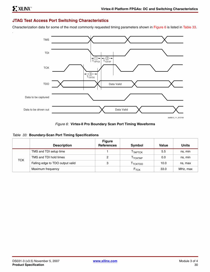
Virtex-II Platform FPGAs: DC and Switching CharacteristicsR
DS031-3 (v3.5) November 5, 2007 www.xilinx.com Module 3 of 4Product Specification 30
JTAG Test Access Port Switching Characteristics
Characterization data for some of the most commonly requested timing parameters shown in Figure 6 is listed in Table 33. FI
Figure 6: Virtex-II Pro Boundary Scan Port Timing Waveforms
Table 33: Boundary-Scan Port Timing Specifications
DescriptionFigure
References Symbol Value Units
TCK
TMS and TDI setup time 1 TTAPTCK 5.5 ns, min
TMS and TDI hold times 2 TTCKTAP 0.0 ns, min
Falling edge to TDO output valid 3 TTCKTDO 10.0 ns, max
Maximum frequency FTCK 33.0 MHz, max
ds083-3_11_012104
Data to be captured
Data to be driven out
TDO
TCK
TDI
TMS
Data Valid
Data Valid
TTCKTDO
TTAPTCK TTCKTAP
1 2
3

Virtex-II Platform FPGAs: DC and Switching CharacteristicsR
DS031-3 (v3.5) November 5, 2007 www.xilinx.com Module 3 of 4Product Specification 31
Virtex-II Pin-to-Pin Output Parameter GuidelinesAll devices are 100% functionally tested. Listed below are representative values for typical pin locations and normal clockloading. Values are expressed in nanoseconds unless otherwise noted.
Global Clock Input to Output Delay for LVTTL, 12 mA, Fast Slew Rate, With DCM
Table 34: Global Clock Input to Output Delay for LVTTL, 12 mA, Fast Slew Rate, With DCM
Description Symbol Device
Speed Grade
Units-6 -5 -4
LVTTL Global Clock Input to Output delay using Output flip-flop, 12 mA, Fast Slew Rate, with DCM.
For data output with different standards, adjust the delays with the values shown in IOB Output Switching Characteristics Standard Adjustments, page 14.
Global Clock and OFF with DCM TICKOFDCM XC2V40 1.10 1.28 1.48 ns
XC2V80 1.10 1.28 1.48 ns
XC2V250 1.10 1.28 1.48 ns
XC2V500 1.10 1.28 1.48 ns
XC2V1000 1.10 1.28 1.48 ns
XC2V1500 1.10 1.28 1.48 ns
XC2V2000 1.10 1.28 1.48 ns
XC2V3000 1.19 1.38 1.59 ns
XC2V4000 1.19 1.38 1.59 ns
XC2V6000 1.64 1.88 2.17 ns
XC2V8000 1.88 2.17 ns
Notes: 1. Listed above are representative values where one global clock input drives one vertical clock line in each accessible column, and
where all accessible IOB and CLB flip-flops are clocked by the global clock net. 2. Output timing is measured at 50% VCC threshold with test setup shown in Figure 1. For other I/O standards, see Table 19.

Virtex-II Platform FPGAs: DC and Switching CharacteristicsR
DS031-3 (v3.5) November 5, 2007 www.xilinx.com Module 3 of 4Product Specification 32
Global Clock Input to Output Delay for LVTTL, 12 mA, Fast Slew Rate, Without DCM
Table 35: Global Clock Input to Output Delay for LVTTL, 12 mA, Fast Slew Rate, Without DCM
Description Symbol Device
Speed Grade
Units-6 -5 -4
LVTTL Global Clock Input to Output Delay using Output flip-flop, 12 mA, Fast Slew Rate, without DCM.
For data output with different standards, adjust the delays with the values shown in IOB Output Switching Characteristics Standard Adjustments, page 14.
Global Clock and OFF without DCM TICKOF XC2V40 3.46 3.58 3.69 ns
XC2V80 3.62 3.58 3.69 ns
XC2V250 3.79 3.88 4.47 ns
XC2V500 3.85 3.88 4.47 ns
XC2V1000 4.02 4.28 4.62 ns
XC2V1500 4.16 4.28 4.62 ns
XC2V2000 4.30 4.43 5.10 ns
XC2V3000 4.49 4.64 5.34 ns
XC2V4000 4.82 4.99 5.74 ns
XC2V6000 5.19 5.38 5.93 ns
XC2V8000 6.09 7.00 ns
Notes: 1. Listed above are representative values where one global clock input drives one vertical clock line in each accessible column, and
where all accessible IOB and CLB flip-flops are clocked by the global clock net. 2. Output timing is measured at 50% VCC threshold with test setup shown in Figure 1. For other I/O standards, see Table 19.

Virtex-II Platform FPGAs: DC and Switching CharacteristicsR
DS031-3 (v3.5) November 5, 2007 www.xilinx.com Module 3 of 4Product Specification 33
Virtex-II Pin-to-Pin Input Parameter GuidelinesAll devices are 100% functionally tested. Listed below are representative values for typical pin locations and normal clockloading. Values are expressed in nanoseconds unless otherwise noted.
Global Clock Setup and Hold for LVTTL Standard, With DCM
Table 36: Global Clock Setup and Hold for LVTTL Standard, With DCM
Description Symbol Device
Speed Grade
Units-6 -5 -4
Input Setup and Hold Time Relative to Global Clock Input Signal for LVTTL Standard.
For data input with different standards, adjust the setup time delay by the values shown in IOB Input Switching Characteristics Standard Adjustments, page 11.
No Delay
Global Clock and IFF with DCM
TPSDCM/TPHDCM XC2V40 1.60/–0.90 1.60/–0.90 1.84/–0.76 ns
XC2V80 1.60/–0.90 1.60/–0.90 1.84/–0.76 ns
XC2V250 1.60/–0.90 1.60/–0.90 1.84/–0.76 ns
XC2V500 1.60/–0.90 1.60/–0.90 1.84/–0.76 ns
XC2V1000 1.60/–0.90 1.60/–0.90 1.84/–0.76 ns
XC2V1500 1.60/–0.90 1.60/–0.90 1.84/–0.76 ns
XC2V2000 1.70/–0.90 1.70/–0.90 1.96/–0.76 ns
XC2V3000 1.70/–0.90 1.70/–0.90 1.96/–0.76 ns
XC2V4000 1.70/–0.90 1.70/–0.90 1.96/–0.76 ns
XC2V6000 1.70/–0.90 1.70/–0.90 1.96/–0.76 ns
XC2V8000 1.70/–0.90 1.96/–0.76 ns
Notes: 1. IFF = Input Flip-Flop or Latch 2. Setup time is measured relative to the Global Clock input signal with the fastest route and the lightest load. Hold time is measured
relative to the Global Clock input signal with the slowest route and heaviest load.

Virtex-II Platform FPGAs: DC and Switching CharacteristicsR
DS031-3 (v3.5) November 5, 2007 www.xilinx.com Module 3 of 4Product Specification 34
Global Clock Setup and Hold for LVTTL Standard, Without DCM ,
Table 37: Global Clock Setup and Hold for LVTTL Standard, Without DCM
Description Symbol Device
Speed Grade
Units-6 -5 -4
Input Setup and Hold Time Relative to Global Clock Input Signal for LVTTL Standard.(2)
For data input with different standards, adjust the setup time delay by the values shown in IOB Input Switching Characteristics Standard Adjustments, page 11.
Full Delay
Global Clock and IFF(1) without DCM
TPSFD/TPHFD XC2V40 1.92/ 0.00 1.92/ 0.00 2.21/ 0.00 ns
XC2V80 2.10/ 0.00 2.10/ 0.00 2.21/ 0.00 ns
XC2V250 1.92/ 0.00 1.92/ 0.00 2.21/ 0.00 ns
XC2V500 1.92/ 0.00 1.92/ 0.00 2.21/ 0.00 ns
XC2V1000 1.92/ 0.00 1.92/ 0.00 2.21/ 0.00 ns
XC2V1500 1.92/ 0.00 1.92/ 0.00 2.21/ 0.00 ns
XC2V2000 1.92/ 0.00 1.92/ 0.00 2.21/ 0.00 ns
XC2V3000 1.92/ 0.00 1.92/ 0.00 2.21/ 0.00 ns
XC2V4000 2.00/ 0.00 2.00/ 0.00 2.30/ 0.00 ns
XC2V6000 1.92/ 0.50 1.92/ 0.50 2.21/ 0.50 ns
XC2V8000 2.38/ 0.00 2.60/ 0.00 ns
Notes: 1. IFF = Input Flip-Flop or Latch2. Setup time is measured relative to the Global Clock input signal with the fastest route and the lightest load. Hold time is measured
relative to the Global Clock input signal with the slowest route and heaviest load.3. These values are parametrically measured.

Virtex-II Platform FPGAs: DC and Switching CharacteristicsR
DS031-3 (v3.5) November 5, 2007 www.xilinx.com Module 3 of 4Product Specification 35
DCM Timing ParametersAll devices are 100% functionally tested. Because of the dif-ficulty in directly measuring many internal timing parame-ters, those parameters are derived from benchmark timingpatterns. The following guidelines reflect worst-case values
across the recommended operating conditions. All outputjitter and phase specifications are determined through sta-tistical measurement at the package pins.
Operating Frequency Rangese
Table 38: Operating Frequency Ranges
Description SymbolConstraint
s
Speed Grade Units-6 -5 -4
Output Clocks (Low Frequency Mode)
CLK0, CLK90, CLK180, CLK270 CLKOUT_FREQ_1X_LF_Min 24.00 24.00 24.00 MHz
CLKOUT_FREQ_1X_LF_Max 230.00 210.00 180.00 MHz
CLK2X, CLK2X180 CLKOUT_FREQ_2X_LF_Min 48.00 48.00 48.00 MHz
CLKOUT_FREQ_2X_LF_Max 450.00 420.00 360.00 MHz
CLKDV CLKOUT_FREQ_DV_LF_Min 1.50 1.50 1.50 MHz
CLKOUT_FREQ_DV_LF_Max 150.00 140.00 120.00 MHz
CLKFX, CLKFX180 CLKOUT_FREQ_FX_LF_Min 24.00 24.00 24.00 MHz
CLKOUT_FREQ_FX_LF_Max 260.00 240.00 210.00 MHz
Input Clocks (Low Frequency Mode)
CLKIN (using DLL outputs) (1,3,4) CLKIN_FREQ_DLL_LF_Min 24.00 24.00 24.00 MHz
CLKIN_FREQ_DLL_LF_Max 230.00 210.00 180.00 MHz
CLKIN (using CLKFX outputs) (2,3,4) CLKIN_FREQ_FX_LF_Min 1.00 1.00 1.00 MHz
CLKIN_FREQ_FX_LF_Max 260.00 240.00 210.00 MHz
PSCLK PSCLK_FREQ_LF_Min 0.01 0.01 0.01 MHz
PSCLK_FREQ_LF_Max 450.00 420.00 360.00 MHz
Output Clocks (High Frequency Mode)
CLK0, CLK180 CLKOUT_FREQ_1X_HF_Min 48.00 48.00 48.00 MHz
CLKOUT_FREQ_1X_HF_Max 450.00 420.00 360.00 MHz
CLKDV CLKOUT_FREQ_DV_HF_Min 3.00 3.00 3.00 MHz
CLKOUT_FREQ_DV_HF_Max 300.00 280.00 240.00 MHz
CLKFX, CLKFX180 CLKOUT_FREQ_FX_HF_Min 210.00 210.00 210.00 MHz
CLKOUT_FREQ_FX_HF_Max 350.00 320.00 270.00 MHz
Input Clocks (High Frequency Mode)
CLKIN (using DLL outputs) (1,3,4) CLKIN_FREQ_DLL_HF_Min 48.00 48.00 48.00 MHz
CLKIN_FREQ_DLL_HF_Max 450.00 420.00 360.00 MHz
CLKIN (using CLKFX outputs) (2,3,4) CLKIN_FRQ_FX_HF_Min 50.00 50.00 50.00 MHz
CLKIN_FRQ_FX_HF_Max 350.00 320.00 270.00 MHz
PSCLK PSCLK_FREQ_HF_Min 0.01 0.01 0.01 MHz
PSCLK_FREQ_HF_Max 450.00 420.00 360.00 MHz
Notes: 1. “DLL outputs” is used here to describe the outputs: CLK0, CLK90, CLK180, CLK270, CLK2X, CLK2X180, and CLKDV.2. If both DLL and CLKFX outputs are used, follow the more restrictive specification.3. If the CLKIN_DIVIDE_BY_2 attribute of the DCM is used, then double these values.4. If the CLKIN_DIVIDE_BY_2 attribute of the DCM is used and CLKIN frequency > 400 MHz, CLKIN duty cycle must be within ±5% (45/55 to 55/45).

Virtex-II Platform FPGAs: DC and Switching CharacteristicsR
DS031-3 (v3.5) November 5, 2007 www.xilinx.com Module 3 of 4Product Specification 36
Input Clock Tolerances
Table 39: Input Clock Tolerances
Description Symbol
Constraints
FCLKIN
Speed Grade
Units
-6 -5 -4
Min Max Min Max Min Max
Input Clock Low/High Pulse Width
PSCLK PSCLK_PULSE < 1MHz 25.00 25.00 25.00 ns
PSCLK and CLKIN(3) PSCLK_PULSE and CLKIN_PULSE
1 – 10 MHz 25.00 25.00 25.00 ns
10 – 25 MHz 10.00 10.00 10.00 ns
25 – 50 MHz 5.00 5.00 5.00 ns
50 – 100 MHz 3.00 3.00 3.00 ns
100 – 150 MHz 2.40 2.40 2.40 ns
150 – 200 MHz 2.00 2.00 2.00 ns
200 – 250 MHz 1.80 1.80 1.80 ns
250 – 300 MHz 1.50 1.50 1.50 ns
300 – 350 MHz 1.30 1.30 1.30 ns
350 – 400 MHz 1.15 1.15 1.15 ns
> 400 MHz 1.05 1.05 1.05 ns
Input Clock Cycle-Cycle Jitter (Low Frequency Mode)
CLKIN (using DLL outputs)(1) CLKIN_CYC_JITT_DLL_LF ±300 ±300 ±300 ps
CLKIN (using CLKFX outputs)(2) CLKIN_CYC_JITT_FX_LF ±300 ±300 ±300 ps
Input Clock Cycle-Cycle Jitter (High Frequency Mode)
CLKIN (using DLL outputs)(1) CLKIN_CYC_JITT_DLL_HF ±150 ±150 ±150 ps
CLKIN (using CLKFX outputs)(2) CLKIN_CYC_JITT_FX_HF ±150 ±150 ±150 ps
Input Clock Period Jitter (Low Frequency Mode)
CLKIN (using DLL outputs)(1) CLKIN_PER_JITT_DLL_LF ±1 ±1 ±1 ns
CLKIN (using CLKFX outputs)(2) CLKIN_PER_JITT_FX_LF ±1 ±1 ±1 ns
Input Clock Period Jitter (High Frequency Mode)
CLKIN (using DLL outputs)(1) CLKIN_PER_JITT_DLL_HF ±1 ±1 ±1 ns
CLKIN (using CLKFX outputs)(2) CLKIN_PER_JITT_FX_HF ±1 ±1 ±1 ns
Feedback Clock Path Delay Variation
CLKFB off-chip feedback CLKFB_DELAY_VAR_EXT ±1 ±1 ±1 ns
Notes: 1. “DLL outputs” is used here to describe the outputs: CLK0, CLK90, CLK180, CLK270, CLK2X, CLK2X180, and CLKDV.2. If both DLL and CLKFX outputs are used, follow the more restrictive specification.3. If DCM phase shift feature is used and CLKIN frequency > 200 Mhz, CLKIN duty cycle must be within ±5% (45/55 to 55/45).

Virtex-II Platform FPGAs: DC and Switching CharacteristicsR
DS031-3 (v3.5) November 5, 2007 www.xilinx.com Module 3 of 4Product Specification 37
Output Clock Jitter
Output Clock Phase Alignment
Table 40: Output Clock Jitter
Description Symbol Constraints
Speed Grade
Units-6 -5 -4
Clock Synthesis Period Jitter
CLK0 CLKOUT_PER_JITT_0 ±100 ±100 ±100 ps
CLK90 CLKOUT_PER_JITT_90 ±150 ±150 ±150 ps
CLK180 CLKOUT_PER_JITT_180 ±150 ±150 ±150 ps
CLK270 CLKOUT_PER_JITT_270 ±150 ±150 ±150 ps
CLK2X, CLK2X180 CLKOUT_PER_JITT_2X ±200 ±200 ±200 ps
CLKDV (integer division) CLKOUT_PER_JITT_DV1 ±150 ±150 ±150 ps
CLKDV (non-integer division) CLKOUT_PER_JITT_DV2 ±300 ±300 ±300 ps
CLKFX, CLKFX180 CLKOUT_PER_JITT_FX Note 1 Note 1 Note 1 ps
Notes: 1. Values for this parameter are available at www.xilinx.com.
Table 41: Output Clock Phase Alignment
Description Symbol Constraints
Speed Grade
Units-6 -5 -4
Phase Offset Between CLKIN and CLKFB
CLKIN/CLKFB CLKIN_CLKFB_PHASE ±50 ±50 ±50 ps
Phase Offset Between Any DCM Outputs
All CLK outputs CLKOUT_PHASE ±140 ±140 ±140 ps
Duty Cycle Precision
DLL outputs(1) CLKOUT_DUTY_CYCLE_DLL(2) ±150 ±150 ±150 ps
CLKFX outputs CLKOUT_DUTY_CYCLE_FX ±100 ±100 ±100 ps
Notes: 1. "DLL outputs" is used here to describe the outputs: CLK0, CLK90, CLK180, CLK270, CLK2X, CLK2X180, and CLKDV.2. CLKOUT_DUTY_CYCLE_DLL applies to the 1X clock outputs (CLK0, CLK90, CLK180, and CLK270) only if
DUTY_CYCLE_CORRECTION = TRUE.3. Specification also applies to PSCLK.

Virtex-II Platform FPGAs: DC and Switching CharacteristicsR
DS031-3 (v3.5) November 5, 2007 www.xilinx.com Module 3 of 4Product Specification 38
Miscellaneous Timing Parameters
Frequency Synthesis
Parameter Cross Reference
Table 42: Miscellaneous Timing Parameters
Description Symbol
Constraints
FCLKIN Speed Grade Units
-6 -5 -4
Time Required to Achieve LOCK
Using DLL outputs(1) LOCK_DLL
LOCK_DLL_60 > 60MHz 20.0 20.0 20.0 μs
LOCK_DLL_50_60 50 - 60 MHz 25.0 25.0 25.0 μs
LOCK_DLL_40_50 40 - 50 MHz 50.0 50.0 50.0 μs
LOCK_DLL_30_40 30 - 40 MHz 90.0 90.0 90.0 μs
LOCK_DLL_24_30 24 - 30 MHz 120.0 120.0 120.0 μs
Using CLKFX outputs LOCK_FX_MIN 10.0 10.0 10.0 ms
LOCK_FX_MAX 10.0 10.0 10.0 ms
Additional lock time with fine-phase shifting
LOCK_DLL_FINE_SHIFT50.0 50.0 50.0 μs
Fine-Phase Shifting
Absolute shifting range FINE_SHIFT_RANGE 10.0 10.0 10.0 ns
Delay Lines
Tap delay resolution DCM_TAP_MIN 30.0 30.0 30.0 ps
DCM_TAP_MAX 60.0 60.0 60.0 ps
Notes: 1. "DLL outputs" is used here to describe the outputs: CLK0, CLK90, CLK180, CLK270, CLK2X, CLK2X180, and CLKDV.2. Specification also applies to PSCLK.
Table 43: Frequency Synthesis
Attribute Min Max
CLKFX_MULTIPLY 2 32
CLKFX_DIVIDE 1 32
Table 44: Parameter Cross Reference
Libraries Guide Data Sheet
DLL_CLKOUT_{MIN|MAX}_LF CLKOUT_FREQ_{1X|2X|DV}_LF
DFS_CLKOUT_{MIN|MAX}_LF CLKOUT_FREQ_FX_LF
DLL_CLKIN_{MIN|MAX}_LF CLKIN_FREQ_DLL_LF
DFS_CLKIN_{MIN|MAX}_LF CLKIN_FREQ_FX_LF
DLL_CLKOUT_{MIN|MAX}_HF CLKOUT_FREQ_{1X|DV}_HF
DFS_CLKOUT_{MIN|MAX}_HF CLKOUT_FREQ_FX_HF
DLL_CLKIN_{MIN|MAX}_HF CLKIN_FREQ_DLL_HF
DFS_CLKIN_{MIN|MAX}_HF CLKIN_FREQ_FX_HF

Virtex-II Platform FPGAs: DC and Switching CharacteristicsR
DS031-3 (v3.5) November 5, 2007 www.xilinx.com Module 3 of 4Product Specification 39
Source-Synchronous Switching CharacteristicsThe parameters in this section provide the necessary values for calculating timing budgets for Virtex-II source-synchronoustransmitter and receiver data-valid windows.
Table 45: Duty Cycle Distortion and Clock-Tree Skew
Description Symbol Device
Speed Grade
Units-6 -5 -4
Duty Cycle Distortion(1) TDCD_CLK0 All 140 140 140 ps
TDCD_CLK180 All 50 50 50 ps
Clock Tree Skew(2) TCKSKEW XC2V40 50 50 60 ps
XC2V80 50 50 60 ps
XC2V250 50 50 60 ps
XC2V500 50 50 60 ps
XC2V1000 80 80 90 ps
XC2V1500 80 80 90 ps
XC2V2000 100 100 110 ps
XC2V3000 100 100 110 ps
XC2V4000 400 400 450 ps
XC2V6000 500 500 550 ps
XC2V8000 600 650 ps
Notes: 1. These parameters represent the worst-case duty cycle distortion observable at the pins of the device using LVDS output buffers. For
cases where other I/O standards are used, IBIS can be used to calculate any additional duty cycle distortion that might be caused by asymmetrical rise/fall times. TDCD_CLK0 applies to cases where local (IOB) inversion is used to provide the negative-edge clock to the DDR element in the I/O. TDCD_CLK180 applies to cases where the CLK180 output of the DCM is used to provide the negative-edge clock to the DDR element in the I/O.
2. This value represents the worst-case clock-tree skew observable between sequential I/O elements. Significantly less clock-tree skew exists for I/O registers that are close to each other and fed by the same or adjacent clock-tree branches. Use the Xilinx FPGA_Editor and Timing Analyzer tools to evaluate clock skew specific to your application.
Table 46: Package Skew
Description Symbol Device/Package Value Units
Package Skew(1) TPKGSKEW XC2V1000 / FF896 130 ps
XC2V3000 / FF1152 115 ps
XC2V3000 / BF957 130 ps
XC2V4000 / FF1152 130 ps
XC2V4000 / FF1517 200 ps
XC2V4000 / BF957 140 ps
XC2V6000 / FF1152 90 ps
XC2V6000 / FF1517 105 ps
XC2V6000 / BF957 105 ps
Notes: 1. These values represent the worst-case skew between any two balls of the package: shortest flight time to longest flight time from Pad
to Ball (7.1ps per mm).2. Package trace length information is available for these device/package combinations. This information can be used to deskew the
package.

Virtex-II Platform FPGAs: DC and Switching CharacteristicsR
DS031-3 (v3.5) November 5, 2007 www.xilinx.com Module 3 of 4Product Specification 40
Table 47: Sample Window
Description Symbol Device
Speed Grade
Units-6 -5 -4
Sampling Error at Receiver Pins(1) TSAMP XC2V40 500 500 550 ps
XC2V80 500 500 550 ps
XC2V250 500 500 550 ps
XC2V500 500 500 550 ps
XC2V1000 500 500 550 ps
XC2V1500 500 500 550 ps
XC2V2000 500 500 550 ps
XC2V3000 500 500 550 ps
XC2V4000 500 500 550 ps
XC2V6000 500 500 550 ps
XC2V8000 500 550 ps
Notes: 1. This parameter indicates the total sampling error of Virtex-II DDR input registers across voltage, temperature, and process. The
characterization methodology uses the DCM to capture the DDR input registers’ edges of operation. These measurements include:- CLK0 and CLK180 DCM jitter- Worst-case Duty-Cycle Distortion - TDCD_CLK180- DCM accuracy (phase offset)- DCM phase shift resolution.These measurements do not include package or clock tree skew.
Table 48: Pin-to-Pin Setup/Hold: Source-Synchronous Configuration
Description Symbol Device
Speed Grade
Units-6 -5 -4
Data Input Set-Up and Hold Times Relative to a Forwarded Clock Input Pin, Using DCM and Global Clock Buffer.
For situations where clock and data inputs conform to different standards, adjust the setup and hold values accordingly using the values shown in IOB Input Switching Characteristics Standard Adjustments, page 11.
No Delay
Global Clock and IFF with DCM
TPSDCM/TPHDCM
XC2V40 0.2/0.5 0.2/0.5 0.2/0.5 ns
XC2V80 0.2/0.5 0.2/0.5 0.2/0.5 ns
XC2V250 0.2/0.5 0.2/0.5 0.2/0.5 ns
XC2V500 0.2/0.5 0.2/0.5 0.2/0.5 ns
XC2V1000 0.2/0.5 0.2/0.5 0.2/0.5 ns
XC2V1500 0.2/0.5 0.2/0.5 0.2/0.5 ns
XC2V2000 0.2/0.5 0.2/0.5 0.2/0.5 ns
XC2V3000 0.2/0.5 0.2/0.5 0.2/0.6 ns
XC2V4000 0.2/0.5 0.2/0.6 0.2/0.6 ns
XC2V6000 0.2/0.5 0.2/0.6 0.2/0.6 ns
XC2V8000 0.2/0.6 0.2/0.7 ns
Notes: 1. IFF = Input Flip-Flop2. The timing values were measured using the fine-phase adjustment feature of the DCM. 3. The worst-case duty-cycle distortion and DCM jitter on CLK0 and CLK180 is included in these measurements.

Virtex-II Platform FPGAs: DC and Switching CharacteristicsR
DS031-3 (v3.5) November 5, 2007 www.xilinx.com Module 3 of 4Product Specification 41
Source Synchronous Timing Budgets
This section describes how to use the parameters provided in the Source-Synchronous Switching Characteristics section todevelop system-specific timing budgets. The following analysis provides information necessary for determining Virtex-IIcontributions to an overall system timing analysis; no assumptions are made about the effects of Inter-Symbol Interferenceor PCB skew.
Virtex-II Transmitter Data-Valid Window (TX)TX is the minimum aggregate valid data period for asource-synchronous data bus at the pins of the device andis calculated as follows:
TX = Data Period - [Jitter(1) + Duty Cycle Distortion(2) + TCKSKEW(3) + TPKGSKEW(4)]
Notes: 1. Jitter values and accumulation methodology to be provided in
a future release of this document. The absolute period jitter values found in the DCM Timing Parameters section of the particular DCM output clock used to clock the IOB FF can be used for a best case analysis.
2. This value depends on the clocking methodology used. See Note1 for Table 45.
3. This value represents the worst-case clock-tree skew observable between sequential I/O elements. Significantly less clock-tree skew exists for I/O registers that are close to each other and fed by the same or adjacent clock-tree branches. Use the Xilinx FPGA_Editor and Timing Analyzer tools to evaluate clock skew specific to your application.
4. These values represent the worst-case skew between any two balls of the package: shortest flight time to longest flight time from Pad to Ball.
Virtex-II Receiver Data-Valid Window (RX)RX is the required minimum aggregate valid data period fora source-synchronous data bus at the pins of the deviceand is calculated as follows:
RX = [TSAMP(1) + TCKSKEW(2) + TPKGSKEW(3) ]
Notes: 1. This parameter indicates the total sampling error of Virtex-II
DDR input registers across voltage, temperature, and process. The characterization methodology uses the DCM to capture the DDR input registers’ edges of operation. These measurements include:- CLK0 and CLK180 DCM jitter in a quiet system- Worst-case duty-cycle distortion- DCM accuracy (phase offset)- DCM phase shift resolution.These measurements do not include package or clock tree skew.
2. This value represents the worst-case clock-tree skew observable between sequential I/O elements. Significantly less clock-tree skew exists for I/O registers that are close to each other and fed by the same or adjacent clock-tree branches. Use the Xilinx FPGA_Editor and Timing Analyzer tools to evaluate clock skew specific to your application.
3. These values represent the worst-case skew between any two balls of the package: shortest flight time to longest flight time from Pad to Ball.
Revision HistoryThis section records the change history for this module of the data sheet.
Date Version Revision
11/07/00 1.0 Early access draft.
12/06/00 1.1 Initial release.
01/15/01 1.2 Added values to the tables in the Virtex-II Performance Characteristics and Virtex-II Switching Characteristics sections.
01/25/01 1.3 • The data sheet was divided into four modules (per the current style standard). • Updated values in the Virtex-II Performance Characteristics and Virtex-II Switching
Characteristics tables.• Table 18, “Delay Measurement Methodology”
04/23/01 1.5 • Updated values in the Virtex-II Performance Characteristics and Virtex-II Switching Characteristics tables.
• Added TREG32 symbol to Table 23.• Skipped v1.4 to sync with other modules. Reverted to traditional double-column format.

Virtex-II Platform FPGAs: DC and Switching CharacteristicsR
DS031-3 (v3.5) November 5, 2007 www.xilinx.com Module 3 of 4Product Specification 42
07/30/01 1.6 • Updated values in the Virtex-II Performance Characteristics and Virtex-II Switching Characteristics tables.
• Added values to the Virtex-II Pin-to-Pin Output Parameter Guidelines and Virtex-II Pin-to-Pin Input Parameter Guidelines tables.
• Added Frequency Synthesis table.
10/02/01 1.7 • Updated values in the Virtex-II Performance Characteristics and Virtex-II Switching Characteristics tables.
• Updated the speed grade designations used in data sheets, and added Table 13, which shows the current speed grade designation for each device.
10/05/01 1.8 • Corrected the speed grade designation for the XC2V1000 device in Table 13.
10/12/01 1.9 • Updated values in the Virtex-II Performance Characteristics and Virtex-II Switching Characteristics tables.
11/28/01 2.0 • Updated values in Table 3, Table 4, Table 5, Virtex-II Performance Characteristics, and Virtex-II Switching Characteristics tables.
01/03/02 2.1 • Updated values in Virtex-II Performance Characteristics and Virtex-II Switching Characteristics tables, based on values extracted from speedsfile version 1.96.
• Changed the speed grade designation for the XC2V6000 device in Table 13.
07/16/02 2.2 • Updated values in Table 4, "Quiescent Supply Current."• Updated values in Virtex-II Performance Characteristics and Virtex-II Switching
Characteristics tables, based on values extracted from speedsfile version 1.111.• Added Enhanced Multiplier Switching Characteristics section.• Added footnote to Table 37, "Global Clock Setup and Hold for LVTTL Standard, Without
DCM."• Added Source-Synchronous Switching Characteristics section.
09/26/02 2.3 • Removed mention of MIL-M-38510/605 specification.• Added footnotes to Table 2 and Table 6.
12/06/02 2.4 • Revised SSTL2 values in Table 6 to match the latest JEDEC specification.• Added footnote regarding VIN PCI compliance to Table 1.• Added footnote regarding CLKOUT_DUTY_CYCLE_DLL to Table 41.
05/07/03 2.5 • Updated values in Virtex-II Performance Characteristics and Virtex-II Switching Characteristics tables, based on values extracted from speedsfile version 1.114.
• Table 4, Quiescent Supply Current, and Table 5, Minimum Power On Current Required for Virtex-II Devices: Added parameters for XC2V8000 device.
• Table 16, IOB Output Switching Characteristics: Changed parameter designator TIOTON to TIOTP.
• Table 26, Enhanced Multiplier Switching Characteristics: Corrected all parameter designators from TMULT_P[nn] to TMULT1_P[nn] in order to correspond with designators used in speedsfile.
• Table 27, Enhanced Pipelined Multiplier Switching Characteristics: Corrected all parameter designators from TMULTCK_P[nn] to TMULTCK1_P[nn] in order to correspond with designators used in speedsfile.
• Removed old Table 19, Standard Capacitive Loads.• Added Figure 1, page 17, showing test configuration for measuring I/O standard
adjustments.
06/19/03 2.5.1 • Removed footnotes in Table 34 and Table 36 that stated DCM jitter was included in the measurements.
Date Version Revision

Virtex-II Platform FPGAs: DC and Switching CharacteristicsR
DS031-3 (v3.5) November 5, 2007 www.xilinx.com Module 3 of 4Product Specification 43
08/01/03 3.0 • Table 13: All Virtex-II devices and speed grades now Production.• Updated values in Virtex-II Performance Characteristics and Virtex-II Switching
Characteristics tables, based on values extracted from speedsfile version 1.116.• Table 34 and Table 35: Revised test setup footnote to refer to Figure 1. Previously
specified a capacitive load parameter.• Figure 1: Added note to figure regarding termination resistors.
10/14/03 3.1 • Table 1: Changed TJ description from “Operating junction temperature” to “Maximum junction temperature”.
• In section General Power Supply Requirements, replaced reference to Answer Record 11713 with reference to XAPP689 regarding handling of simultaneously switching outputs (SSO).
• In section I/O Standard Adjustment Measurement Methodology:- Table 18 renamed Input Delay Measurement Methodology. Added footnotes.- Added new Table 19, Output Delay Measurement Methodology. - Replaced Figure 1, Generalized Test Setup, with new drawing. - Revised and extended text describing output delay measurement procedure.
• Table 45, Table 47, and Table 48: All Source-Synchronous parameters for all devices now available in these tables.
• XC2V8000 is no longer offered in the -6 speed grade. The following tables containing parameters or other references to this device/grade combination were corrected accordingly: Table 13, Table 14, Table 34, Table 35, Table 36, Table 37, Table 45, Table 47, and Table 48.
• Table 39: For Input Clock Low/High Pulse Width, PSCLK and CLKIN, changed existing Footnote (2) to new Footnote (3).
03/29/04 3.2 • Table 4: - For XC2V40, added Maximum quiescent supply current specifications.- For all devices, updated Typical specifications for ICCINTQ and ICCAUXQ.
• Section Power-On Power Supply Requirements, page 3: Added Footnote (1) qualifying statement that power supplies can be turned on in any sequence.
• Added section Configuration Timing, page 27. This section includes new timing diagrams as well as parameter specification tables formerly included in the Virtex-II Platform FPGA User Guide.
• Table 20, Clock Distribution Switching Characteristics: Added parameter TGSI/TGIS (Global Clock Buffer S Input Setup/Hold to I1 and I2 Inputs).
• Table 38, Operating Frequency Ranges: Added Footnote (4) to all four CLKIN parameters.
• Recompiled for backward compatibility with Acrobat 4 and above.
06/24/04 3.3 • Table 1: Added TSOL parameters for Pb-free package devices.
03/01/05 3.4 • Updated values in Virtex-II Performance Characteristics and Virtex-II Switching Characteristics tables, based on values extracted from speedsfile version 1.120.
• Table 2: Corrected Footnote (1) to require connecting VBATT to VCCAUX or GND if battery is not used.
• Table 3: Corrected "VREF current per bank" to "VREF current per pin."• Section Power-On Power Supply Requirements: Added word “monotonically” to
description of supply voltage ramp-on requirements. Added sentence to footnote (1) indicating that if the stated requirements are violated, no damage to the device will result, but configuration will probably fail.
• Figure 3 and Figure 4: Corrected to show DOUT transitions driven by falling edge of CCLK.
Date Version Revision

Virtex-II Platform FPGAs: DC and Switching CharacteristicsR
DS031-3 (v3.5) November 5, 2007 www.xilinx.com Module 3 of 4Product Specification 44
Notice of DisclaimerTHE XILINX HARDWARE FPGA AND CPLD DEVICES REFERRED TO HEREIN (“PRODUCTS”) ARE SUBJECT TO THE TERMS ANDCONDITIONS OF THE XILINX LIMITED WARRANTY WHICH CAN BE VIEWED AT http://www.xilinx.com/warranty.htm. THIS LIMITEDWARRANTY DOES NOT EXTEND TO ANY USE OF PRODUCTS IN AN APPLICATION OR ENVIRONMENT THAT IS NOT WITHIN THESPECIFICATIONS STATED IN THE XILINX DATA SHEET. ALL SPECIFICATIONS ARE SUBJECT TO CHANGE WITHOUT NOTICE.PRODUCTS ARE NOT DESIGNED OR INTENDED TO BE FAIL-SAFE OR FOR USE IN ANY APPLICATION REQUIRING FAIL-SAFEPERFORMANCE, SUCH AS LIFE-SUPPORT OR SAFETY DEVICES OR SYSTEMS, OR ANY OTHER APPLICATION THAT INVOKESTHE POTENTIAL RISKS OF DEATH, PERSONAL INJURY, OR PROPERTY OR ENVIRONMENTAL DAMAGE (“CRITICALAPPLICATIONS”). USE OF PRODUCTS IN CRITICAL APPLICATIONS IS AT THE SOLE RISK OF CUSTOMER, SUBJECT TOAPPLICABLE LAWS AND REGULATIONS.
Virtex-II Data SheetThe Virtex-II Data Sheet contains the following modules:
• Virtex-II Platform FPGAs: Introduction and Overview (Module 1)
• Virtex-II Platform FPGAs: Functional Description (Module 2)
• Virtex-II Platform FPGAs: DC and Switching Characteristics (Module 3)
• Virtex-II Platform FPGAs: Pinout Information (Module 4)
03/01/05(cont’d)
3.4(cont’d)
• Table 15, Table 17, Table 18, and Table 19: Restructured these I/O-related tables to include descriptions, as well as the actual IOSTANDARD attributes (used in Xilinx ISE™ software) for all I/O standards.
• Table 15: Added data for the following I/O standards: SSTL18_I, SSTL18_II, SSTL18_I_DCI, SSTL18_II_DCI, HSTL_I_18, HSTL_II_18, HSTL_III_18, HSTL_IV_18, LVDSEXT_25, LVDSEXT_33, BLVDS_25, LVDS_25_DCI, LVDS_33_DCI, LVDSEXT_25_DCI, LVDSEXT_33_DCI, HSLVDCI_15, HSLVDCI_18, HSLVDCI_25, HSLVDCI_33. Rearranged I/O standards in a more logical order.
• Table 16: Added parameter TRPW (Minimum Pulse Width, SR Input).• Table 17: Added data for the following I/O standards: SSTL18_I, SSTL18_II,
SSTL18_I_DCI, SSTL18_II_DCI, HSLVDCI_15, HSLVDCI_18, HSLVDCI_25, HSLVDCI_33. Changed “Csl” to “CREF” to agree with Figure 1 and Table 19. Rearranged I/O standards in a more logical order.
• Table 18: Added data for the following I/O standards: SSTL18_I, SSTL18_II, HSTL_I_18, HSTL_II_18, HSTL_III_18, HSTL_IV_18. Added footnote defining equivalents for DCI standards.
• Table 19: Added Footnotes (2) and (3) to PCI/PCI-X capacitive load (CREF) values. Added HSLVDCI callouts to LVDCI parameter rows (same values).
• Table 28: Added parameter TBCCS, CLKA to CLKB Setup Time.• Table 31: Added Footnote (1) indicating that FCC_SERIAL should not exceed
FCC_STARTUP if no provision is made to adjust the speed of CCLK.• Table 33: TTCKTDO corrected from a “Min” to a “Max” specification.
11/05/07 3.5 • Updated copyright notice and legal disclaimer.
Date Version Revision

© 2000–2007 Xilinx, Inc. All rights reserved. XILINX, the Xilinx logo, the Brand Window, and other designated brands included herein are trademarks of Xilinx, Inc. All other trademarks are the property of their respective owners.
DS031-4 (v3.5) November 5, 2007 www.xilinx.com Module 4 of 4Product Specification 1
This document provides Virtex-II™ Device/Package Combi-nations, Maximum I/Os Available, and Virtex-II Pin Defini-tions, followed by pinout tables for the following packages:
• CS144/CSG144 Chip-Scale BGA Package• FG256/FGG256 Fine-Pitch BGA Package• FG456/FGG456 Fine-Pitch BGA Package• FG676/FGG676 Fine-Pitch BGA Package• BG575/BGG575 Standard BGA Package
• BG728/BGG728 Standard BGA Package • FF896 Flip-Chip Fine-Pitch BGA Package• FF1152 Flip-Chip Fine-Pitch BGA Package• FF1517 Flip-Chip Fine-Pitch BGA Package• BF957 Flip-Chip BGA Package
For device pinout diagrams and layout guidelines, refer tothe Virtex-II Platform FPGA User Guide. ASCII packagepinout files are also available for download from the Xilinxwebsite (www.xilinx.com).
Virtex-II Device/Package Combinations and Maximum I/Os AvailableWire-bond and flip-chip packages are available. Table 1 andTable 2 show the maximum number of user I/Os possible inwire-bond and flip-chip packages, respectively.
Table 3 shows the number of user I/Os available for alldevice/package combinations.
• CS denotes wire-bond chip-scale ball grid array (BGA) (0.80 mm pitch).
• CSG denotes Pb-free wire-bond chip-scale ball grid array (BGA) (0.80 mm pitch).
• FG denotes wire-bond fine-pitch BGA (1.00 mm pitch).
• FGG denotes Pb-free wire-bond fine-pitch BGA (1.00 mm pitch).
• BG denotes standard BGA (1.27 mm pitch).• BGG denotes Pb-free standard BGA (1.27 mm pitch).• FF denotes flip-chip fine-pitch BGA (1.00 mm pitch).• BF denotes flip-chip BGA (1.27 mm pitch).
The number of I/Os per package include all user I/Os exceptthe 15 control pins (CCLK, DONE, M0, M1, M2, PROG_B,PWRDWN_B, TCK, TDI, TDO, TMS, HSWAP_EN, DXN,DXP, AND RSVD).
226
Virtex-II Platform FPGAs:Pinout Information
DS031-4 (v3.5) November 5, 2007 Product Specification
R
Table 1: Wire-Bond Packages Information
Package(1)CS144/CSG144
FG256/FGG256
FG456/FGG456
FG676/FGG676
BG575/BGG575
BG728/BGG728
Pitch (mm) 0.80 1.00 1.00 1.00 1.27 1.27
Size (mm) 12 x 12 17 x 17 23 x 23 27 x 27 31 x 31 35 x 35
I/Os 92 172 324 484 408 516
Notes: 1. Wire-bond packages include FGGnnn Pb-free versions. See Virtex-II Ordering Examples (Module 1).
Table 2: Flip-Chip Packages Information
Package FF896 FF1152 FF1517 BF957
Pitch (mm) 1.00 1.00 1.00 1.27
Size (mm) 31 x 31 35 x 35 40 x 40 40 x 40
I/Os 624 824 1,108 684

Virtex-II Platform FPGAs: Pinout InformationR
DS031-4 (v3.5) November 5, 2007 www.xilinx.com Module 4 of 4Product Specification 2
Virtex-II Pin DefinitionsThis section describes the pinouts for Virtex-II devices in thefollowing packages:
• CS144: wire-bond chip-scale ball grid array (BGA) of 0.80 mm pitch
• FG256, FG456, and FG676: wire-bond fine-pitch BGA of 1.00 mm pitch
• FF896, FF1152, FF1517: flip-chip fine-pitch BGA of 1.00 mm pitch
• BG575 and BG728: wire-bond BGA of 1.27 mm pitch
• BF957: flip-chip BGA of 1.27 mm pitch
All of the devices supported in a particular package arepinout compatible and are listed in the same table (onetable per package). In addition, the FG456 and FG676packages are compatible, as are the FF896 and FF1152packages. Pins that are not available for the smallestdevices are listed in right-hand columns.
Each device is split into eight I/O banks to allow for flexibilityin the choice of I/O standards (see the Virtex-II Data Sheet).Global pins, including JTAG, configuration, andpower/ground pins, are listed at the end of each table.Table 4 provides definitions for all pin types.
The FG256 pinouts (Table 6) is included as an example. AllVirtex-II pinout tables are available on the distributionCD-ROM, or on the web (at http://www.xilinx.com).
Table 3: Virtex-II Device/Package Combinations and Maximum Number of Available I/Os
Package
Available I/Os
XC2V40
XC2V80
XC2V250
XC2V500
XC2V1000
XC2V1500
XC2V2000
XC2V3000
XC2V4000
XC2V6000
XC2V8000
CS144 88 92 92 - - - - - - - -
FG256 88 120 172 172 172 - - - - - -
FG456 - - 200 264 324 - - - - - -
FG676 - - - - - 392 456 484 - - -
FF896 - - - - 432 528 624 - - - -
FF1152 - - - - - - - 720 824 824 824
FF1517 - - - - - - - - 912 1,104 1,108
BG575 - - - - 328 392 408 - - - -
BG728 - - - - - - - 516 - - -
BF957 - - - - - - 624 684 684 684 -

Virtex-II Platform FPGAs: Pinout InformationR
DS031-4 (v3.5) November 5, 2007 www.xilinx.com Module 4 of 4Product Specification 3
Pin DefinitionsTable 4 provides a description of each pin type listed in Virtex-II pinout tables.
Table 4: Virtex-II Pin Definitions
Pin Name Direction Description
User I/O Pins
IO_LXXY_# Input/Output/Bidirectional
All user I/O pins are capable of differential signalling and can implement LVDS, ULVDS, BLVDS, LVPECL, or LDT pairs. Each user I/O is labeled “IO_LXXY_#”, where:
IO indicates a user I/O pin.LXXY indicates a differential pair, with XX a unique pair in the bank and Y = P/N for the positive and negative sides of the differential pair.# indicates the bank number (0 through 7)
Dual-Function Pins
IO_LXXY_#/ZZZ The dual-function pins are labelled “IO_LXXY_#/ZZZ”, where ZZZ can be one of the following pins:Per Bank - VRP, VRN, or VREF Globally - GCLKX(S/P), BUSY/DOUT, INIT_B, D0/DIN – D7, RDWR_B, or CS_B
With /ZZZ:
D0/DIN, D1, D2, D3, D4, D5, D6, D7
Input/Output • In SelectMAP mode, D0 through D7 are configuration data pins. These pins become user I/Os after configuration, unless the SelectMAP port is retained.
• In bit-serial modes, DIN (D0) is the single-data input. This pin becomes a user I/O after configuration.
CS_B Input In SelectMAP mode, this is the active-low Chip Select signal. The pin becomes a user I/O after configuration, unless the SelectMAP port is retained.
RDWR_B Input In SelectMAP mode, this is the active-low Write Enable signal. The pin becomes a user I/O after configuration, unless the SelectMAP port is retained.
BUSY/DOUT Output • In SelectMAP mode, BUSY controls the rate at which configuration data is loaded. The pin becomes a user I/O after configuration, unless the SelectMAP port is retained.
• In bit-serial modes, DOUT provides preamble and configuration data to downstream devices in a daisy-chain. The pin becomes a user I/O after configuration.
INIT_B Bidirectional (open-drain)
When Low, this pin indicates that the configuration memory is being cleared. When held Low, the start of configuration is delayed. During configuration, a Low on this output indicates that a configuration data error has occurred. The pin becomes a user I/O after configuration.
GCLKx (S/P) Input/Output These are clock input pins that connect to Global Clock Buffers. These pins become regular user I/Os when not needed for clocks.
VRP Input This pin is for the DCI voltage reference resistor of P transistor (per bank).
VRN Input This pin is for the DCI voltage reference resistor of N transistor (per bank).
ALT_VRP Input This is the alternative pin for the DCI voltage reference resistor of P transistor.
ALT_VRN Input This is the alternative pin for the DCI voltage reference resistor of N transistor.
VREF Input These are input threshold voltage pins. They become user I/Os when an external threshold voltage is not needed (per bank).
Dedicated Pins(1)
CCLK Input/Output Configuration clock. Output in Master mode or Input in Slave mode.

Virtex-II Platform FPGAs: Pinout InformationR
DS031-4 (v3.5) November 5, 2007 www.xilinx.com Module 4 of 4Product Specification 4
PROG_B Input Active Low asynchronous reset to configuration logic. This pin has a permanent weak pull-up resistor.
DONE Input/Output DONE is a bidirectional signal with an optional internal pull-up resistor. As an output, this pin indicates completion of the configuration process. As an input, a Low level on DONE can be configured to delay the start-up sequence.
M2, M1, M0 Input Configuration mode selection.
HSWAP_EN Input Enable I/O pull-ups during configuration.
TCK Input Boundary Scan Clock.
TDI Input Boundary Scan Data Input.
TDO Output Boundary Scan Data Output.
TMS Input Boundary Scan Mode Select.
PWRDWN_B Input(unsupported)
Active Low power-down pin (unsupported). Driving this pin Low can adversely affect device operation and configuration. PWRDWN_B is internally pulled High, which is its default state. It does not require an external pull-up.
Other Pins
DXN, DXP N/A Temperature-sensing diode pins (Anode: DXP, Cathode: DXN).
VBATT Input Decryptor key memory backup supply. Connect VBATT to VCCAUX or GND if battery is not used.
RSVD N/A Reserved pin - do not connect.
VCCO Input Power-supply pins for the output drivers (per bank).
VCCAUX Input Power-supply pins for auxiliary circuits.
VCCINT Input Power-supply pins for the internal core logic.
GND Input Ground.
Notes: 1. All dedicated pins (JTAG and configuration) are powered by VCCAUX (independent of the bank VCCO voltage).
Table 4: Virtex-II Pin Definitions (Continued)
Pin Name Direction Description

Virtex-II Platform FPGAs: Pinout InformationR
DS031-4 (v3.5) November 5, 2007 www.xilinx.com Module 4 of 4Product Specification 5
CS144/CSG144 Chip-Scale BGA PackageAs shown in Table 5, XC2V40, XC2V80, and XC2V250 Virtex-II devices are available in the CS144/CSG144 package. Pinsin the XC2V40, XC2V80, and XC2V250 devices are the same except for pin differences in the XC2V40 device, shown in theNo Connect column. Following this table are the CS144/CSG144 Chip-Scale BGA Package Specifications (0.80mm pitch).
Table 5: CS144/CSG144 — XC2V40, XC2V80, and XC2V250
Bank Pin Description Pin Number No Connect in the XC2V40
0 IO_L01N_0 B3
0 IO_L01P_0 A3
0 IO_L02N_0 C4
0 IO_L02P_0 B4
0 IO_L03N_0/VRP_0 A4
0 IO_L03P_0/VRN_0 D5
0 IO_L94N_0/VREF_0 A5
0 IO_L94P_0 D6
0 IO_L95N_0/GCLK7P C6
0 IO_L95P_0/GCLK6S B6
0 IO_L96N_0/GCLK5P A6
0 IO_L96P_0/GCLK4S D7
1 IO_L96N_1/GCLK3P A7
1 IO_L96P_1/GCLK2S B7
1 IO_L95N_1/GCLK1P A8
1 IO_L95P_1/GCLK0S B8
1 IO_L94N_1 C8
1 IO_L94P_1/VREF_1 D8
1 IO_L03N_1/VRP_1 C9
1 IO_L03P_1/VRN_1 D9
1 IO_L02N_1 A10
1 IO_L02P_1 B10
1 IO_L01N_1 C10
1 IO_L01P_1 D10
2 IO_L01N_2 C13
2 IO_L01P_2 D11
2 IO_L02N_2/VRP_2 D12
2 IO_L02P_2/VRN_2 D13
2 IO_L03N_2 E10
2 IO_L03P_2/VREF_2 E11
2 IO_L93N_2 E13 NC
2 IO_L93P_2/VREF_2 F11 NC
2 IO_L94N_2 F12
2 IO_L94P_2 G10

Virtex-II Platform FPGAs: Pinout InformationR
DS031-4 (v3.5) November 5, 2007 www.xilinx.com Module 4 of 4Product Specification 6
2 IO_L96N_2 G11
2 IO_L96P_2 G13
3 IO_L96N_3 G12
3 IO_L96P_3 H12
3 IO_L94N_3 H11
3 IO_L94P_3 J13
3 IO_L03N_3/VREF_3 J10
3 IO_L03P_3 K13
3 IO_L02N_3/VRP_3 K12
3 IO_L02P_3/VRN_3 K11
3 IO_L01N_3 K10
3 IO_L01P_3 L13
4 IO_L01N_4/BUSY/DOUT(1) M11
4 IO_L01P_4/INIT_B N11
4 IO_L02N_4/D0/DIN(1) L10
4 IO_L02P_4/D1 M10
4 IO_L03N_4/D2/ALT_VRP_4 N10
4 IO_L03P_4/D3/ALT_VRN_4 K9
4 IO_L94N_4/VREF_4 N9
4 IO_L94P_4 K8
4 IO_L95N_4/GCLK3S L8
4 IO_L95P_4/GCLK2P M8
4 IO_L96N_4/GCLK1S N8
4 IO_L96P_4/GCLK0P K7
5 IO_L96N_5/GCLK7S N7
5 IO_L96P_5/GCLK6P M7
5 IO_L95N_5/GCLK5S N6
5 IO_L95P_5/GCLK4P M6
5 IO_L94N_5 L6
5 IO_L94P_5/VREF_5 K6
5 IO_L03N_5/D4/ALT_VRP_5 L5
5 IO_L03P_5/D5/ALT_VRN_5 K5
5 IO_L02N_5/D6 N4
5 IO_L02P_5/D7 M4
5 IO_L01N_5/RDWR_B L4
5 IO_L01P_5/CS_B K4
Table 5: CS144/CSG144 — XC2V40, XC2V80, and XC2V250
Bank Pin Description Pin Number No Connect in the XC2V40

Virtex-II Platform FPGAs: Pinout InformationR
DS031-4 (v3.5) November 5, 2007 www.xilinx.com Module 4 of 4Product Specification 7
6 IO_L01P_6 L3
6 IO_L01N_6 L2
6 IO_L02P_6/VRN_6 L1
6 IO_L02N_6/VRP_6 K3
6 IO_L03P_6 K2
6 IO_L03N_6/VREF_6 K1
6 IO_L94P_6 J2
6 IO_L94N_6 H4
6 IO_L96P_6 H3
6 IO_L96N_6 H1
7 IO_L96P_7 G4
7 IO_L96N_7 G3
7 IO_L94P_7 G1
7 IO_L94N_7 F1
7 IO_L93P_7/VREF_7 F2 NC
7 IO_L93N_7 F4 NC
7 IO_L03P_7/VREF_7 E2
7 IO_L03N_7 E3
7 IO_L02P_7/VRN_7 E4
7 IO_L02N_7/VRP_7 D1
7 IO_L01P_7 D2
7 IO_L01N_7 D3
0 VCCO_0 B5
0 VCCO_0 C3
1 VCCO_1 A11
1 VCCO_1 A9
2 VCCO_2 F10
2 VCCO_2 C12
3 VCCO_3 L12
3 VCCO_3 J12
4 VCCO_4 M9
4 VCCO_4 L11
5 VCCO_5 N3
5 VCCO_5 N5
6 VCCO_6 J3
6 VCCO_6 M1
7 VCCO_7 D4
7 VCCO_7 F3
Table 5: CS144/CSG144 — XC2V40, XC2V80, and XC2V250
Bank Pin Description Pin Number No Connect in the XC2V40

Virtex-II Platform FPGAs: Pinout InformationR
DS031-4 (v3.5) November 5, 2007 www.xilinx.com Module 4 of 4Product Specification 8
NA CCLK M13
NA PROG_B B1
NA DONE N12
NA M0 N2
NA M1 M2
NA M2 M3
NA TCK B12
NA TDI C1
NA TDO C11
NA TMS A13
NA PWRDWN_B M12
NA HSWAP_EN A1
NA RSVD A2
NA RSVD B2
NA VBATT A12
NA RSVD B11
NA VCCAUX C2
NA VCCAUX N1
NA VCCAUX N13
NA VCCAUX B13
NA VCCINT H2
NA VCCINT L7
NA VCCINT H13
NA VCCINT C7
NA GND E1
NA GND G2
NA GND J1
NA GND J4
NA GND M5
NA GND L9
NA GND J11
NA GND H10
NA GND F13
NA GND E12
NA GND B9
NA GND C5
Notes: 1. See Table 4 for an explanation of the signals available on this pin.
Table 5: CS144/CSG144 — XC2V40, XC2V80, and XC2V250
Bank Pin Description Pin Number No Connect in the XC2V40

Virtex-II Platform FPGAs: Pinout InformationR
DS031-4 (v3.5) November 5, 2007 www.xilinx.com Module 4 of 4Product Specification 9
CS144/CSG144 Chip-Scale BGA Package Specifications (0.80mm pitch)
Figure 1: CS144/CSG144 Chip-Scale BGA Package Specifications

Virtex-II Platform FPGAs: Pinout InformationR
DS031-4 (v3.5) November 5, 2007 www.xilinx.com Module 4 of 4Product Specification 10
FG256/FGG256 Fine-Pitch BGA PackageAs shown in Table 6, XC2V40, XC2V80, XC2V250, XC2V500, and XC2V1000 Virtex-II devices are available in theFG256/FGG256 fine-pitch BGA package. The pins in the XC2V250, XC2V500, and XC2V1000 devices are same. The NoConnect columns show pin differences for the XC2V40 and XC2V80 devices. Following this table are the FG256/FGG256Fine-Pitch BGA Package Specifications (1.00mm pitch).
Table 6: FG256/FGG256 BGA — XC2V40, XC2V80, XC2V250, XC2V500, and XC2V1000
Bank Pin Description Pin Number No Connect in XC2V40 No Connect in XC2V80
0 IO_L01N_0 C4
0 IO_L01P_0 B4
0 IO_L02N_0 D5
0 IO_L02P_0 C5
0 IO_L03N_0/VRP_0 B5
0 IO_L03P_0/VRN_0 A5
0 IO_L04N_0/VREF_0 D6 NC NC
0 IO_L04P_0 C6 NC NC
0 IO_L05N_0 B6 NC NC
0 IO_L05P_0 A6 NC NC
0 IO_L92N_0 E6 NC NC
0 IO_L92P_0 E7 NC NC
0 IO_L93N_0 D7 NC NC
0 IO_L93P_0 C7 NC NC
0 IO_L94N_0/VREF_0 B7
0 IO_L94P_0 A7
0 IO_L95N_0/GCLK7P D8
0 IO_L95P_0/GCLK6S C8
0 IO_L96N_0/GCLK5P B8
0 IO_L96P_0/GCLK4S A8
1 IO_L96N_1/GCLK3P A9
1 IO_L96P_1/GCLK2S B9
1 IO_L95N_1/GCLK1P C9
1 IO_L95P_1/GCLK0S D9
1 IO_L94N_1 A10
1 IO_L94P_1/VREF_1 B10
1 IO_L93N_1 C10 NC NC
1 IO_L93P_1 D10 NC NC
1 IO_L92N_1 E10 NC NC

Virtex-II Platform FPGAs: Pinout InformationR
DS031-4 (v3.5) November 5, 2007 www.xilinx.com Module 4 of 4Product Specification 11
1 IO_L92P_1 E11 NC NC
1 IO_L05N_1 A11 NC NC
1 IO_L05P_1 B11 NC NC
1 IO_L04N_1 C11 NC NC
1 IO_L04P_1/VREF_1 D11 NC NC
1 IO_L03N_1/VRP_1 A12
1 IO_L03P_1/VRN_1 B12
1 IO_L02N_1 C12
1 IO_L02P_1 D12
1 IO_L01N_1 B13
1 IO_L01P_1 C13
2 IO_L01N_2 C16
2 IO_L01P_2 D16
2 IO_L02N_2/VRP_2 D14
2 IO_L02P_2/VRN_2 D15
2 IO_L03N_2 E13
2 IO_L03P_2/VREF_2 E14
2 IO_L04N_2 E15 NC
2 IO_L04P_2 E16 NC
2 IO_L06N_2 F13 NC
2 IO_L06P_2 F14 NC
2 IO_L43N_2 F15 NC NC
2 IO_L43P_2 F16 NC NC
2 IO_L45N_2 F12 NC NC
2 IO_L45P_2/VREF_2 G12 NC NC
2 IO_L91N_2 G13 NC
2 IO_L91P_2 G14 NC
2 IO_L93N_2 G15 NC
2 IO_L93P_2/VREF_2 G16 NC
2 IO_L94N_2 H13
2 IO_L94P_2 H14
2 IO_L96N_2 H15
2 IO_L96P_2 H16
Table 6: FG256/FGG256 BGA — XC2V40, XC2V80, XC2V250, XC2V500, and XC2V1000
Bank Pin Description Pin Number No Connect in XC2V40 No Connect in XC2V80

Virtex-II Platform FPGAs: Pinout InformationR
DS031-4 (v3.5) November 5, 2007 www.xilinx.com Module 4 of 4Product Specification 12
3 IO_L96N_3 J16
3 IO_L96P_3 J15
3 IO_L94N_3 J14
3 IO_L94P_3 J13
3 IO_L93N_3/VREF_3 K16 NC
3 IO_L93P_3 K15 NC
3 IO_L91N_3 K14 NC
3 IO_L91P_3 K13 NC
3 IO_L45N_3/VREF_3 K12 NC NC
3 IO_L45P_3 L12 NC NC
3 IO_L43N_3 L16 NC NC
3 IO_L43P_3 L15 NC NC
3 IO_L06N_3 L14 NC
3 IO_L06P_3 L13 NC
3 IO_L04N_3 M16 NC
3 IO_L04P_3 M15 NC
3 IO_L03N_3/VREF_3 M14
3 IO_L03P_3 M13
3 IO_L02N_3/VRP_3 N15
3 IO_L02P_3/VRN_3 N14
3 IO_L01N_3 N16
3 IO_L01P_3 P16
4 IO_L01N_4/BUSY/DOUT(1) T14
4 IO_L01P_4/INIT_B T13
4 IO_L02N_4/D0/DIN(1) P13
4 IO_L02P_4/D1 R13
4 IO_L03N_4/D2/ALT_VRP_4 N12
4 IO_L03P_4/D3/ALT_VRN_4 P12
4 IO_L04N_4/VREF_4 R12 NC NC
4 IO_L04P_4 T12 NC NC
4 IO_L05N_4/VRP_4 N11 NC NC
4 IO_L05P_4/VRN_4 P11 NC NC
Table 6: FG256/FGG256 BGA — XC2V40, XC2V80, XC2V250, XC2V500, and XC2V1000
Bank Pin Description Pin Number No Connect in XC2V40 No Connect in XC2V80

Virtex-II Platform FPGAs: Pinout InformationR
DS031-4 (v3.5) November 5, 2007 www.xilinx.com Module 4 of 4Product Specification 13
4 IO_L91N_4/VREF_4 R11 NC NC
4 IO_L91P_4 T11 NC NC
4 IO_L92N_4 M11 NC NC
4 IO_L92P_4 M10 NC NC
4 IO_L93N_4 N10 NC NC
4 IO_L93P_4 P10 NC NC
4 IO_L94N_4/VREF_4 R10
4 IO_L94P_4 T10
4 IO_L95N_4/GCLK3S N9
4 IO_L95P_4/GCLK2P P9
4 IO_L96N_4/GCLK1S R9
4 IO_L96P_4/GCLK0P T9
5 IO_L96N_5/GCLK7S T8
5 IO_L96P_5/GCLK6P R8
5 IO_L95N_5/GCLK5S P8
5 IO_L95P_5/GCLK4P N8
5 IO_L94N_5 T7
5 IO_L94P_5/VREF_5 R7
5 IO_L93N_5 P7 NC NC
5 IO_L93P_5 N7 NC NC
5 IO_L92N_5 M7 NC NC
5 IO_L92P_5 M6 NC NC
5 IO_L91N_5 T6 NC NC
5 IO_L91P_5/VREF_5 R6 NC NC
5 IO_L05N_5/VRP_5 P6 NC NC
5 IO_L05P_5/VRN_5 N6 NC NC
5 IO_L04N_5 T5 NC NC
5 IO_L04P_5/VREF_5 R5 NC NC
5 IO_L03N_5/D4/ALT_VRP_5 P5
5 IO_L03P_5/D5/ALT_VRN_5 N5
5 IO_L02N_5/D6 R4
5 IO_L02P_5/D7 P4
5 IO_L01N_5/RDWR_B T4
Table 6: FG256/FGG256 BGA — XC2V40, XC2V80, XC2V250, XC2V500, and XC2V1000
Bank Pin Description Pin Number No Connect in XC2V40 No Connect in XC2V80

Virtex-II Platform FPGAs: Pinout InformationR
DS031-4 (v3.5) November 5, 2007 www.xilinx.com Module 4 of 4Product Specification 14
5 IO_L01P_5/CS_B T3
6 IO_L01P_6 P1
6 IO_L01N_6 N1
6 IO_L02P_6/VRN_6 N3
6 IO_L02N_6/VRP_6 N2
6 IO_L03P_6 M4
6 IO_L03N_6/VREF_6 M3
6 IO_L04P_6 M2 NC
6 IO_L04N_6 M1 NC
6 IO_L06P_6 L4 NC
6 IO_L06N_6 L3 NC
6 IO_L43P_6 L2 NC NC
6 IO_L43N_6 L1 NC NC
6 IO_L45P_6 L5 NC NC
6 IO_L45N_6/VREF_6 K5 NC NC
6 IO_L91P_6 K4 NC
6 IO_L91N_6 K3 NC
6 IO_L93P_6 K2 NC
6 IO_L93N_6/VREF_6 K1 NC
6 IO_L94P_6 J4
6 IO_L94N_6 J3
6 IO_L96P_6 J2
6 IO_L96N_6 J1
7 IO_L96P_7 H1
7 IO_L96N_7 H2
7 IO_L94P_7 H3
7 IO_L94N_7 H4
7 IO_L93P_7/VREF_7 G1 NC
7 IO_L93N_7 G2 NC
7 IO_L91P_7 G3 NC
7 IO_L91N_7 G4 NC
7 IO_L45P_7/VREF_7 G5 NC NC
Table 6: FG256/FGG256 BGA — XC2V40, XC2V80, XC2V250, XC2V500, and XC2V1000
Bank Pin Description Pin Number No Connect in XC2V40 No Connect in XC2V80

Virtex-II Platform FPGAs: Pinout InformationR
DS031-4 (v3.5) November 5, 2007 www.xilinx.com Module 4 of 4Product Specification 15
7 IO_L45N_7 F5 NC NC
7 IO_L43P_7 F1 NC NC
7 IO_L43N_7 F2 NC NC
7 IO_L06P_7 F3 NC
7 IO_L06N_7 F4 NC
7 IO_L04P_7 E1 NC
7 IO_L04N_7 E2 NC
7 IO_L03P_7/VREF_7 E3
7 IO_L03N_7 E4
7 IO_L02P_7/VRN_7 D2
7 IO_L02N_7/VRP_7 D3
7 IO_L01P_7 D1
7 IO_L01N_7 C1
0 VCCO_0 F8
0 VCCO_0 F7
0 VCCO_0 E8
1 VCCO_1 F10
1 VCCO_1 F9
1 VCCO_1 E9
2 VCCO_2 H12
2 VCCO_2 H11
2 VCCO_2 G11
3 VCCO_3 K11
3 VCCO_3 J12
3 VCCO_3 J11
4 VCCO_4 M9
4 VCCO_4 L10
4 VCCO_4 L9
5 VCCO_5 M8
5 VCCO_5 L8
5 VCCO_5 L7
6 VCCO_6 K6
6 VCCO_6 J6
Table 6: FG256/FGG256 BGA — XC2V40, XC2V80, XC2V250, XC2V500, and XC2V1000
Bank Pin Description Pin Number No Connect in XC2V40 No Connect in XC2V80

Virtex-II Platform FPGAs: Pinout InformationR
DS031-4 (v3.5) November 5, 2007 www.xilinx.com Module 4 of 4Product Specification 16
6 VCCO_6 J5
7 VCCO_7 H6
7 VCCO_7 H5
7 VCCO_7 G6
NA CCLK P15
NA PROG_B A2
NA DONE R14
NA M0 T2
NA M1 P2
NA M2 R3
NA HSWAP_EN B3
NA TCK A15
NA TDI C2
NA TDO C15
NA TMS B14
NA PWRDWN_B T15
NA RSVD A4
NA RSVD A3
NA VBATT A14
NA RSVD A13
NA VCCAUX R16
NA VCCAUX R1
NA VCCAUX B16
NA VCCAUX B1
NA VCCINT N13
NA VCCINT N4
NA VCCINT M12
NA VCCINT M5
NA VCCINT E12
NA VCCINT E5
NA VCCINT D13
NA VCCINT D4
Table 6: FG256/FGG256 BGA — XC2V40, XC2V80, XC2V250, XC2V500, and XC2V1000
Bank Pin Description Pin Number No Connect in XC2V40 No Connect in XC2V80

Virtex-II Platform FPGAs: Pinout InformationR
DS031-4 (v3.5) November 5, 2007 www.xilinx.com Module 4 of 4Product Specification 17
NA GND T16
NA GND T1
NA GND R15
NA GND R2
NA GND P14
NA GND P3
NA GND L11
NA GND L6
NA GND K10
NA GND K9
NA GND K8
NA GND K7
NA GND J10
NA GND J9
NA GND J8
NA GND J7
NA GND H10
NA GND H9
NA GND H8
NA GND H7
NA GND G10
NA GND G9
NA GND G8
NA GND G7
NA GND F11
NA GND F6
NA GND C14
NA GND C3
NA GND B15
NA GND B2
NA GND A16
NA GND A1
Notes: 1. See Table 4 for an explanation of the signals available on this pin.
Table 6: FG256/FGG256 BGA — XC2V40, XC2V80, XC2V250, XC2V500, and XC2V1000
Bank Pin Description Pin Number No Connect in XC2V40 No Connect in XC2V80

Virtex-II Platform FPGAs: Pinout InformationR
DS031-4 (v3.5) November 5, 2007 www.xilinx.com Module 4 of 4Product Specification 18
FG256/FGG256 Fine-Pitch BGA Package Specifications (1.00mm pitch)
Figure 2: FG256/FGG256 Fine-Pitch BGA Package Specifications

Virtex-II Platform FPGAs: Pinout InformationR
DS031-4 (v3.5) November 5, 2007 www.xilinx.com Module 4 of 4Product Specification 19
FG456/FGG456 Fine-Pitch BGA PackageAs shown in Table 7, XC2V250, XC2V500, and XC2V1000 Virtex-II devices are available in the FG456/FGG456 fine-pitchBGA package. Pins in the XC2V250, XC2V500, and XC2V1000 devices are the same, except for the pin differences in theXC2V250 and XC2V500 devices shown in the No Connect columns. Following this table are the FG456/FGG456 Fine-PitchBGA Package Specifications (1.00mm pitch).
Table 7: FG456/FGG456 BGA — XC2V250, XC2V500, and XC2V1000
Bank Pin Description Pin Number No Connect in XC2V250 No Connect in XC2V500
0 IO_L01N_0 B4
0 IO_L01P_0 A4
0 IO_L02N_0 C4
0 IO_L02P_0 C5
0 IO_L03N_0/VRP_0 B5
0 IO_L03P_0/VRN_0 A5
0 IO_L04N_0/VREF_0 D6
0 IO_L04P_0 C6
0 IO_L05N_0 B6
0 IO_L05P_0 A6
0 IO_L06N_0 E7
0 IO_L06P_0 E8
0 IO_L21N_0 D7 NC NC
0 IO_L21P_0/VREF_0 C7 NC NC
0 IO_L22N_0 B7 NC NC
0 IO_L22P_0 A7 NC NC
0 IO_L24N_0 D8 NC NC
0 IO_L24P_0 C8 NC NC
0 IO_L49N_0 B8 NC
0 IO_L49P_0 A8 NC
0 IO_L51N_0 E9 NC
0 IO_L51P_0/VREF_0 F9 NC
0 IO_L52N_0 D9 NC
0 IO_L52P_0 C9 NC
0 IO_L54N_0 B9 NC
0 IO_L54P_0 A9 NC
0 IO_L91N_0/VREF_0 E10
0 IO_L91P_0 F10
0 IO_L92N_0 D10
0 IO_L92P_0 C10

Virtex-II Platform FPGAs: Pinout InformationR
DS031-4 (v3.5) November 5, 2007 www.xilinx.com Module 4 of 4Product Specification 20
0 IO_L93N_0 B10
0 IO_L93P_0 A10
0 IO_L94N_0/VREF_0 E11
0 IO_L94P_0 F11
0 IO_L95N_0/GCLK7P D11
0 IO_L95P_0/GCLK6S C11
0 IO_L96N_0/GCLK5P B11
0 IO_L96P_0/GCLK4S A11
1 IO_L96N_1/GCLK3P F12
1 IO_L96P_1/GCLK2S F13
1 IO_L95N_1/GCLK1P E12
1 IO_L95P_1/GCLK0S D12
1 IO_L94N_1 C12
1 IO_L94P_1/VREF_1 B12
1 IO_L93N_1 A13
1 IO_L93P_1 B13
1 IO_L92N_1 C13
1 IO_L92P_1 D13
1 IO_L91N_1 E13
1 IO_L91P_1/VREF_1 E14
1 IO_L54N_1 A14 NC
1 IO_L54P_1 B14 NC
1 IO_L52N_1 C14 NC
1 IO_L52P_1 D14 NC
1 IO_L51N_1/VREF_1 A15 NC
1 IO_L51P_1 B15 NC
1 IO_L49N_1 C15 NC
1 IO_L49P_1 D15 NC
1 IO_L24N_1 F14 NC NC
1 IO_L24P_1 E15 NC NC
1 IO_L22N_1 A16 NC NC
1 IO_L22P_1 B16 NC NC
1 IO_L21N_1/VREF_1 C16 NC NC
Table 7: FG456/FGG456 BGA — XC2V250, XC2V500, and XC2V1000
Bank Pin Description Pin Number No Connect in XC2V250 No Connect in XC2V500

Virtex-II Platform FPGAs: Pinout InformationR
DS031-4 (v3.5) November 5, 2007 www.xilinx.com Module 4 of 4Product Specification 21
1 IO_L21P_1 D16 NC NC
1 IO_L06N_1 E16
1 IO_L06P_1 E17
1 IO_L05N_1 A17
1 IO_L05P_1 B17
1 IO_L04N_1 C17
1 IO_L04P_1/VREF_1 D17
1 IO_L03N_1/VRP_1 A18
1 IO_L03P_1/VRN_1 B18
1 IO_L02N_1 C18
1 IO_L02P_1 D18
1 IO_L01N_1 A19
1 IO_L01P_1 B19
2 IO_L01N_2 C21
2 IO_L01P_2 C22
2 IO_L02N_2/VRP_2 E18
2 IO_L02P_2/VRN_2 F18
2 IO_L03N_2 D21
2 IO_L03P_2/VREF_2 D22
2 IO_L04N_2 E19
2 IO_L04P_2 E20
2 IO_L06N_2 E21
2 IO_L06P_2 E22
2 IO_L19N_2 F19 NC NC
2 IO_L19P_2 F20 NC NC
2 IO_L21N_2 F21 NC NC
2 IO_L21P_2/VREF_2 F22 NC NC
2 IO_L22N_2 G18 NC NC
2 IO_L22P_2 H18 NC NC
2 IO_L24N_2 G19 NC NC
2 IO_L24P_2 G20 NC NC
2 IO_L43N_2 G21
2 IO_L43P_2 G22
Table 7: FG456/FGG456 BGA — XC2V250, XC2V500, and XC2V1000
Bank Pin Description Pin Number No Connect in XC2V250 No Connect in XC2V500

Virtex-II Platform FPGAs: Pinout InformationR
DS031-4 (v3.5) November 5, 2007 www.xilinx.com Module 4 of 4Product Specification 22
2 IO_L45N_2 H19
2 IO_L45P_2/VREF_2 H20
2 IO_L46N_2 H21
2 IO_L46P_2 H22
2 IO_L48N_2 J17
2 IO_L48P_2 J18
2 IO_L49N_2 J19 NC
2 IO_L49P_2 J20 NC
2 IO_L51N_2 J21 NC
2 IO_L51P_2/VREF_2 J22 NC
2 IO_L52N_2 K17 NC
2 IO_L52P_2 K18 NC
2 IO_L54N_2 K19 NC
2 IO_L54P_2 K20 NC
2 IO_L91N_2 K21
2 IO_L91P_2 K22
2 IO_L93N_2 L17
2 IO_L93P_2/VREF_2 L18
2 IO_L94N_2 L19
2 IO_L94P_2 L20
2 IO_L96N_2 L21
2 IO_L96P_2 L22
3 IO_L96N_3 M21
3 IO_L96P_3 M20
3 IO_L94N_3 M19
3 IO_L94P_3 M18
3 IO_L93N_3/VREF_3 M17
3 IO_L93P_3 N17
3 IO_L91N_3 N22
3 IO_L91P_3 N21
3 IO_L54N_3 N20 NC
3 IO_L54P_3 N19 NC
3 IO_L52N_3 N18 NC
Table 7: FG456/FGG456 BGA — XC2V250, XC2V500, and XC2V1000
Bank Pin Description Pin Number No Connect in XC2V250 No Connect in XC2V500

Virtex-II Platform FPGAs: Pinout InformationR
DS031-4 (v3.5) November 5, 2007 www.xilinx.com Module 4 of 4Product Specification 23
3 IO_L52P_3 P18 NC
3 IO_L51N_3/VREF_3 P22 NC
3 IO_L51P_3 P21 NC
3 IO_L49N_3 P20 NC
3 IO_L49P_3 P19 NC
3 IO_L48N_3 R22
3 IO_L48P_3 R21
3 IO_L46N_3 R20
3 IO_L46P_3 R19
3 IO_L45N_3/VREF_3 R18
3 IO_L45P_3 P17
3 IO_L43N_3 T22
3 IO_L43P_3 T21
3 IO_L24N_3 T20 NC NC
3 IO_L24P_3 T19 NC NC
3 IO_L22N_3 U22 NC NC
3 IO_L22P_3 U21 NC NC
3 IO_L21N_3/VREF_3 U20 NC NC
3 IO_L21P_3 U19 NC NC
3 IO_L19N_3 T18 NC NC
3 IO_L19P_3 U18 NC NC
3 IO_L06N_3 V22
3 IO_L06P_3 V21
3 IO_L04N_3 V20
3 IO_L04P_3 V19
3 IO_L03N_3/VREF_3 W22
3 IO_L03P_3 W21
3 IO_L02N_3/VRP_3 Y22
3 IO_L02P_3/VRN_3 Y21
3 IO_L01N_3 W20
3 IO_L01P_3 AA20
4 IO_L01N_4/BUSY/DOUT(1) AB19
4 IO_L01P_4/INIT_B AA19
Table 7: FG456/FGG456 BGA — XC2V250, XC2V500, and XC2V1000
Bank Pin Description Pin Number No Connect in XC2V250 No Connect in XC2V500

Virtex-II Platform FPGAs: Pinout InformationR
DS031-4 (v3.5) November 5, 2007 www.xilinx.com Module 4 of 4Product Specification 24
4 IO_L02N_4/D0/DIN(1) V18
4 IO_L02P_4/D1 V17
4 IO_L03N_4/D2/ALT_VRP_4 W18
4 IO_L03P_4/D3/ALT_VRN_4 Y18
4 IO_L04N_4/VREF_4 AA18
4 IO_L04P_4 AB18
4 IO_L05N_4/VRP_4 W17
4 IO_L05P_4/VRN_4 Y17
4 IO_L06N_4 AA17
4 IO_L06P_4 AB17
4 IO_L19N_4 V16 NC NC
4 IO_L19P_4 V15 NC NC
4 IO_L21N_4 W16 NC NC
4 IO_L21P_4/VREF_4 Y16 NC NC
4 IO_L22N_4 AA16 NC NC
4 IO_L22P_4 AB16 NC NC
4 IO_L24N_4 W15 NC NC
4 IO_L24P_4 Y15 NC NC
4 IO_L49N_4 AA15 NC
4 IO_L49P_4 AB15 NC
4 IO_L51N_4 U14 NC
4 IO_L51P_4/VREF_4 V14 NC
4 IO_L52N_4 W14 NC
4 IO_L52P_4 Y14 NC
4 IO_L54N_4 AA14 NC
4 IO_L54P_4 AB14 NC
4 IO_L91N_4/VREF_4 U13
4 IO_L91P_4 V13
4 IO_L92N_4 W13
4 IO_L92P_4 Y13
4 IO_L93N_4 AA13
4 IO_L93P_4 AB13
4 IO_L94N_4/VREF_4 U12
4 IO_L94P_4 V12
Table 7: FG456/FGG456 BGA — XC2V250, XC2V500, and XC2V1000
Bank Pin Description Pin Number No Connect in XC2V250 No Connect in XC2V500

Virtex-II Platform FPGAs: Pinout InformationR
DS031-4 (v3.5) November 5, 2007 www.xilinx.com Module 4 of 4Product Specification 25
4 IO_L95N_4/GCLK3S W12
4 IO_L95P_4/GCLK2P Y12
4 IO_L96N_4/GCLK1S AA12
4 IO_L96P_4/GCLK0P AB12
5 IO_L96N_5/GCLK7S AA11
5 IO_L96P_5/GCLK6P Y11
5 IO_L95N_5/GCLK5S W11
5 IO_L95P_5/GCLK4P V11
5 IO_L94N_5 U11
5 IO_L94P_5/VREF_5 U10
5 IO_L93N_5 AB10
5 IO_L93P_5 AA10
5 IO_L92N_5 Y10
5 IO_L92P_5 W10
5 IO_L91N_5 V10
5 IO_L91P_5/VREF_5 V9
5 IO_L54N_5 AB9 NC
5 IO_L54P_5 AA9 NC
5 IO_L52N_5 Y9 NC
5 IO_L52P_5 W9 NC
5 IO_L51N_5/VREF_5 AB8 NC
5 IO_L51P_5 AA8 NC
5 IO_L49N_5 Y8 NC
5 IO_L49P_5 W8 NC
5 IO_L24N_5 U9 NC NC
5 IO_L24P_5 V8 NC NC
5 IO_L22N_5 AB7 NC NC
5 IO_L22P_5 AA7 NC NC
5 IO_L21N_5/VREF_5 Y7 NC NC
5 IO_L21P_5 W7 NC NC
5 IO_L19N_5 AB6 NC NC
5 IO_L19P_5 AA6 NC NC
5 IO_L06N_5 Y6
Table 7: FG456/FGG456 BGA — XC2V250, XC2V500, and XC2V1000
Bank Pin Description Pin Number No Connect in XC2V250 No Connect in XC2V500

Virtex-II Platform FPGAs: Pinout InformationR
DS031-4 (v3.5) November 5, 2007 www.xilinx.com Module 4 of 4Product Specification 26
5 IO_L06P_5 W6
5 IO_L05N_5/VRP_5 V7
5 IO_L05P_5/VRN_5 V6
5 IO_L04N_5 AB5
5 IO_L04P_5/VREF_5 AA5
5 IO_L03N_5/D4/ALT_VRP_5 Y5
5 IO_L03P_5/D5/ALT_VRN_5 W5
5 IO_L02N_5/D6 AB4
5 IO_L02P_5/D7 AA4
5 IO_L01N_5/RDWR_B Y4
5 IO_L01P_5/CS_B AA3
6 IO_L01P_6 V5
6 IO_L01N_6 U5
6 IO_L02P_6/VRN_6 Y2
6 IO_L02N_6/VRP_6 Y1
6 IO_L03P_6 V4
6 IO_L03N_6/VREF_6 V3
6 IO_L04P_6 W2
6 IO_L04N_6 W1
6 IO_L06P_6 U4
6 IO_L06N_6 U3
6 IO_L19P_6 V2 NC NC
6 IO_L19N_6 V1 NC NC
6 IO_L21P_6 U2 NC NC
6 IO_L21N_6/VREF_6 U1 NC NC
6 IO_L22P_6 T5 NC NC
6 IO_L22N_6 R5 NC NC
6 IO_L24P_6 T4 NC NC
6 IO_L24N_6 T3 NC NC
6 IO_L43P_6 T2
6 IO_L43N_6 T1
6 IO_L45P_6 R4
6 IO_L45N_6/VREF_6 R3
Table 7: FG456/FGG456 BGA — XC2V250, XC2V500, and XC2V1000
Bank Pin Description Pin Number No Connect in XC2V250 No Connect in XC2V500

Virtex-II Platform FPGAs: Pinout InformationR
DS031-4 (v3.5) November 5, 2007 www.xilinx.com Module 4 of 4Product Specification 27
6 IO_L46P_6 R2
6 IO_L46N_6 R1
6 IO_L48P_6 P6
6 IO_L48N_6 P5
6 IO_L49P_6 P4 NC
6 IO_L49N_6 P3 NC
6 IO_L51P_6 P2 NC
6 IO_L51N_6/VREF_6 P1 NC
6 IO_L52P_6 N6 NC
6 IO_L52N_6 N5 NC
6 IO_L54P_6 N4 NC
6 IO_L54N_6 N3 NC
6 IO_L91P_6 N2
6 IO_L91N_6 N1
6 IO_L93P_6 M6
6 IO_L93N_6/VREF_6 M5
6 IO_L94P_6 M4
6 IO_L94N_6 M3
6 IO_L96P_6 M2
6 IO_L96N_6 M1
7 IO_L96P_7 L2
7 IO_L96N_7 L3
7 IO_L94P_7 L4
7 IO_L94N_7 L5
7 IO_L93P_7/VREF_7 K1
7 IO_L93N_7 K2
7 IO_L91P_7 K3
7 IO_L91N_7 K4
7 IO_L54P_7 L6 NC
7 IO_L54N_7 K6 NC
7 IO_L52P_7 K5 NC
7 IO_L52N_7 J5 NC
7 IO_L51P_7/VREF_7 J1 NC
Table 7: FG456/FGG456 BGA — XC2V250, XC2V500, and XC2V1000
Bank Pin Description Pin Number No Connect in XC2V250 No Connect in XC2V500

Virtex-II Platform FPGAs: Pinout InformationR
DS031-4 (v3.5) November 5, 2007 www.xilinx.com Module 4 of 4Product Specification 28
7 IO_L51N_7 J2 NC
7 IO_L49P_7 J3 NC
7 IO_L49N_7 J4 NC
7 IO_L48P_7 H1
7 IO_L48N_7 H2
7 IO_L46P_7 H3
7 IO_L46N_7 H4
7 IO_L45P_7/VREF_7 J6
7 IO_L45N_7 H5
7 IO_L43P_7 G1
7 IO_L43N_7 G2
7 IO_L24P_7 G3 NC NC
7 IO_L24N_7 G4 NC NC
7 IO_L22P_7 F1 NC NC
7 IO_L22N_7 F2 NC NC
7 IO_L21P_7/VREF_7 F3 NC NC
7 IO_L21N_7 F4 NC NC
7 IO_L19P_7 G5 NC NC
7 IO_L19N_7 F5 NC NC
7 IO_L06P_7 E1
7 IO_L06N_7 E2
7 IO_L04P_7 E3
7 IO_L04N_7 E4
7 IO_L03P_7/VREF_7 D1
7 IO_L03N_7 D2
7 IO_L02P_7/VRN_7 C1
7 IO_L02N_7/VRP_7 C2
7 IO_L01P_7 E5
7 IO_L01N_7 E6
0 VCCO_0 G11
0 VCCO_0 G10
0 VCCO_0 G9
0 VCCO_0 F8
Table 7: FG456/FGG456 BGA — XC2V250, XC2V500, and XC2V1000
Bank Pin Description Pin Number No Connect in XC2V250 No Connect in XC2V500

Virtex-II Platform FPGAs: Pinout InformationR
DS031-4 (v3.5) November 5, 2007 www.xilinx.com Module 4 of 4Product Specification 29
0 VCCO_0 F7
1 VCCO_1 G14
1 VCCO_1 G13
1 VCCO_1 G12
1 VCCO_1 F16
1 VCCO_1 F15
2 VCCO_2 L16
2 VCCO_2 K16
2 VCCO_2 J16
2 VCCO_2 H17
2 VCCO_2 G17
3 VCCO_3 T17
3 VCCO_3 R17
3 VCCO_3 P16
3 VCCO_3 N16
3 VCCO_3 M16
4 VCCO_4 U16
4 VCCO_4 U15
4 VCCO_4 T14
4 VCCO_4 T13
4 VCCO_4 T12
5 VCCO_5 U8
5 VCCO_5 U7
5 VCCO_5 T11
5 VCCO_5 T10
5 VCCO_5 T9
6 VCCO_6 T6
6 VCCO_6 R6
6 VCCO_6 P7
6 VCCO_6 N7
6 VCCO_6 M7
7 VCCO_7 L7
7 VCCO_7 K7
7 VCCO_7 J7
Table 7: FG456/FGG456 BGA — XC2V250, XC2V500, and XC2V1000
Bank Pin Description Pin Number No Connect in XC2V250 No Connect in XC2V500
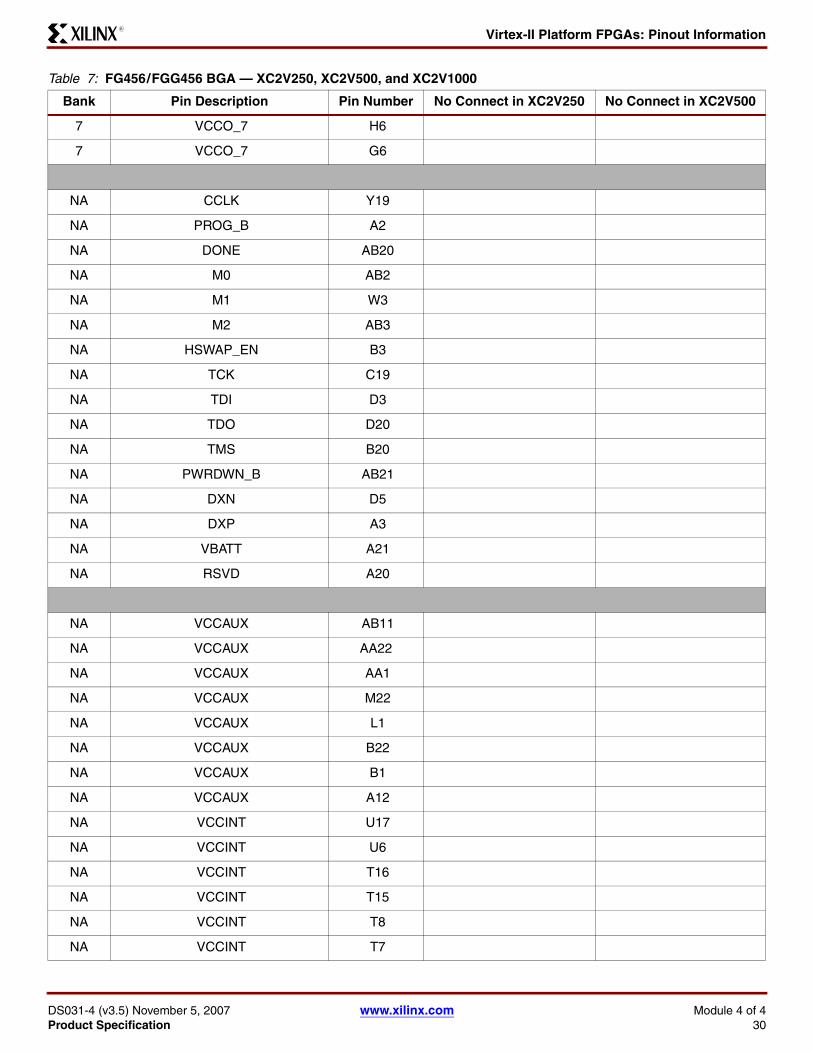
Virtex-II Platform FPGAs: Pinout InformationR
DS031-4 (v3.5) November 5, 2007 www.xilinx.com Module 4 of 4Product Specification 30
7 VCCO_7 H6
7 VCCO_7 G6
NA CCLK Y19
NA PROG_B A2
NA DONE AB20
NA M0 AB2
NA M1 W3
NA M2 AB3
NA HSWAP_EN B3
NA TCK C19
NA TDI D3
NA TDO D20
NA TMS B20
NA PWRDWN_B AB21
NA DXN D5
NA DXP A3
NA VBATT A21
NA RSVD A20
NA VCCAUX AB11
NA VCCAUX AA22
NA VCCAUX AA1
NA VCCAUX M22
NA VCCAUX L1
NA VCCAUX B22
NA VCCAUX B1
NA VCCAUX A12
NA VCCINT U17
NA VCCINT U6
NA VCCINT T16
NA VCCINT T15
NA VCCINT T8
NA VCCINT T7
Table 7: FG456/FGG456 BGA — XC2V250, XC2V500, and XC2V1000
Bank Pin Description Pin Number No Connect in XC2V250 No Connect in XC2V500

Virtex-II Platform FPGAs: Pinout InformationR
DS031-4 (v3.5) November 5, 2007 www.xilinx.com Module 4 of 4Product Specification 31
NA VCCINT R16
NA VCCINT R7
NA VCCINT H16
NA VCCINT H7
NA VCCINT G16
NA VCCINT G15
NA VCCINT G8
NA VCCINT G7
NA VCCINT F17
NA VCCINT F6
NA GND AB22
NA GND AB1
NA GND AA21
NA GND AA2
NA GND Y20
NA GND Y3
NA GND W19
NA GND W4
NA GND P14
NA GND P13
NA GND P12
NA GND P11
NA GND P10
NA GND P9
NA GND N14
NA GND N13
NA GND N12
NA GND N11
NA GND N10
NA GND N9
NA GND M14
NA GND M13
NA GND M12
NA GND M11
Table 7: FG456/FGG456 BGA — XC2V250, XC2V500, and XC2V1000
Bank Pin Description Pin Number No Connect in XC2V250 No Connect in XC2V500

Virtex-II Platform FPGAs: Pinout InformationR
DS031-4 (v3.5) November 5, 2007 www.xilinx.com Module 4 of 4Product Specification 32
NA GND M10
NA GND M9
NA GND L14
NA GND L13
NA GND L12
NA GND L11
NA GND L10
NA GND L9
NA GND K14
NA GND K13
NA GND K12
NA GND K11
NA GND K10
NA GND K9
NA GND J14
NA GND J13
NA GND J12
NA GND J11
NA GND J10
NA GND J9
NA GND D19
NA GND D4
NA GND C20
NA GND C3
NA GND B21
NA GND B2
NA GND A22
NA GND A1
Notes: 1. See Table 4 for an explanation of the signals available on this pin.
Table 7: FG456/FGG456 BGA — XC2V250, XC2V500, and XC2V1000
Bank Pin Description Pin Number No Connect in XC2V250 No Connect in XC2V500

Virtex-II Platform FPGAs: Pinout InformationR
DS031-4 (v3.5) November 5, 2007 www.xilinx.com Module 4 of 4Product Specification 33
FG456/FGG456 Fine-Pitch BGA Package Specifications (1.00mm pitch)
Figure 3: FG456/FGG456 Fine-Pitch BGA Package Specifications

Virtex-II Platform FPGAs: Pinout InformationR
DS031-4 (v3.5) November 5, 2007 www.xilinx.com Module 4 of 4Product Specification 34
FG676/FGG676 Fine-Pitch BGA PackageAs shown in Table 8, XC2V1500, XC2V2000, and XC2V3000 Virtex-II devices are available in the FG676/FGG676 fine-pitchBGA package. Pins in the XC2V1500, XC2V2000, and XC2V3000 devices are the same, except for the pin differences in theXC2V1500 and XC2V2000 devices shown in the No Connect columns. Following this table are the FG676/FGG676Fine-Pitch BGA Package Specifications (1.00mm pitch).
Table 8: FG676/FGG676 BGA — XC2V1500, XC2V2000, and XC2V3000
Bank Pin Description Pin Number No Connect in XC2V1500 No Connect in XC2V2000
0 IO_L01N_0 D6
0 IO_L01P_0 C6
0 IO_L02N_0 B1
0 IO_L02P_0 A2
0 IO_L03N_0/VRP_0 D7
0 IO_L03P_0/VRN_0 C7
0 IO_L04N_0/VREF_0 B3
0 IO_L04P_0 A3
0 IO_L05N_0 G6
0 IO_L05P_0 G7
0 IO_L06N_0 E6
0 IO_L06P_0 E7
0 IO_L19N_0 B4
0 IO_L19P_0 A4
0 IO_L21N_0 B5
0 IO_L21P_0/VREF_0 A5
0 IO_L22N_0 B6
0 IO_L22P_0 A6
0 IO_L24N_0 A7
0 IO_L24P_0 A8
0 IO_L25N_0 E8 NC NC
0 IO_L25P_0 D8 NC NC
0 IO_L27N_0 G8 NC NC
0 IO_L27P_0/VREF_0 F8 NC NC
0 IO_L49N_0 C8
0 IO_L49P_0 B8
0 IO_L51N_0 D9
0 IO_L51P_0/VREF_0 E9
0 IO_L52N_0 F9
0 IO_L52P_0 G9
0 IO_L54N_0 B9
0 IO_L54P_0 A9
0 IO_L67N_0 C9

Virtex-II Platform FPGAs: Pinout InformationR
DS031-4 (v3.5) November 5, 2007 www.xilinx.com Module 4 of 4Product Specification 35
0 IO_L67P_0 C10
0 IO_L69N_0 F10
0 IO_L69P_0/VREF_0 G10
0 IO_L70N_0 E10
0 IO_L70P_0 D10
0 IO_L72N_0 A10
0 IO_L72P_0 A11
0 IO_L73N_0 F11 NC
0 IO_L73P_0 E11 NC
0 IO_L75N_0 G11 NC
0 IO_L75P_0/VREF_0 H11 NC
0 IO_L76N_0 D11 NC
0 IO_L76P_0 C11 NC
0 IO_L78N_0 B11 NC
0 IO_L78P_0 B12 NC
0 IO_L91N_0/VREF_0 G12
0 IO_L91P_0 H12
0 IO_L92N_0 F12
0 IO_L92P_0 E12
0 IO_L93N_0 D12
0 IO_L93P_0 C12
0 IO_L94N_0/VREF_0 G13
0 IO_L94P_0 H13
0 IO_L95N_0/GCLK7P F13
0 IO_L95P_0/GCLK6S E13
0 IO_L96N_0/GCLK5P D13
0 IO_L96P_0/GCLK4S C13
1 IO_L96N_1/GCLK3P H14
1 IO_L96P_1/GCLK2S H15
1 IO_L95N_1/GCLK1P G14
1 IO_L95P_1/GCLK0S F14
1 IO_L94N_1 E14
1 IO_L94P_1/VREF_1 D14
1 IO_L93N_1 A12
1 IO_L93P_1 A13
1 IO_L92N_1 A14
Table 8: FG676/FGG676 BGA — XC2V1500, XC2V2000, and XC2V3000
Bank Pin Description Pin Number No Connect in XC2V1500 No Connect in XC2V2000

Virtex-II Platform FPGAs: Pinout InformationR
DS031-4 (v3.5) November 5, 2007 www.xilinx.com Module 4 of 4Product Specification 36
1 IO_L92P_1 A15
1 IO_L91N_1 B15
1 IO_L91P_1/VREF_1 C15
1 IO_L78N_1 D15 NC
1 IO_L78P_1 E15 NC
1 IO_L76N_1 F15 NC
1 IO_L76P_1 G15 NC
1 IO_L75N_1/VREF_1 G16 NC
1 IO_L75P_1 F16 NC
1 IO_L73N_1 A16 NC
1 IO_L73P_1 A17 NC
1 IO_L72N_1 B16
1 IO_L72P_1 C16
1 IO_L70N_1 D16
1 IO_L70P_1 E16
1 IO_L69N_1/VREF_1 C17
1 IO_L69P_1 D17
1 IO_L67N_1 H16
1 IO_L67P_1 G17
1 IO_L54N_1 E17
1 IO_L54P_1 F17
1 IO_L52N_1 A18
1 IO_L52P_1 A19
1 IO_L51N_1/VREF_1 E18
1 IO_L51P_1 D18
1 IO_L49N_1 B18
1 IO_L49P_1 C18
1 IO_L27N_1/VREF_1 F19 NC NC
1 IO_L27P_1 F18 NC NC
1 IO_L25N_1 G18 NC NC
1 IO_L25P_1 G19 NC NC
1 IO_L24N_1 B19
1 IO_L24P_1 C19
1 IO_L22N_1 D19
1 IO_L22P_1 E19
1 IO_L21N_1/VREF_1 A20
1 IO_L21P_1 A21
Table 8: FG676/FGG676 BGA — XC2V1500, XC2V2000, and XC2V3000
Bank Pin Description Pin Number No Connect in XC2V1500 No Connect in XC2V2000

Virtex-II Platform FPGAs: Pinout InformationR
DS031-4 (v3.5) November 5, 2007 www.xilinx.com Module 4 of 4Product Specification 37
1 IO_L19N_1 E20
1 IO_L19P_1 F20
1 IO_L06N_1 B21
1 IO_L06P_1 B22
1 IO_L05N_1 A22
1 IO_L05P_1 A23
1 IO_L04N_1 C21
1 IO_L04P_1/VREF_1 D21
1 IO_L03N_1/VRP_1 C20
1 IO_L03P_1/VRN_1 D20
1 IO_L02N_1 A24
1 IO_L02P_1 A25
1 IO_L01N_1 B23
1 IO_L01P_1 B24
2 IO_L01N_2 B26
2 IO_L01P_2 C26
2 IO_L02N_2/VRP_2 G20
2 IO_L02P_2/VRN_2 H20
2 IO_L03N_2 C25
2 IO_L03P_2/VREF_2 D25
2 IO_L04N_2 E23
2 IO_L04P_2 E24
2 IO_L06N_2 G21
2 IO_L06P_2 G22
2 IO_L19N_2 D26
2 IO_L19P_2 E26
2 IO_L21N_2 F23
2 IO_L21P_2/VREF_2 F24
2 IO_L22N_2 E25
2 IO_L22P_2 F25
2 IO_L24N_2 H22
2 IO_L24P_2 H21
2 IO_L25N_2 G23 NC NC
2 IO_L25P_2 G24 NC NC
2 IO_L43N_2 F26
2 IO_L43P_2 G26
Table 8: FG676/FGG676 BGA — XC2V1500, XC2V2000, and XC2V3000
Bank Pin Description Pin Number No Connect in XC2V1500 No Connect in XC2V2000

Virtex-II Platform FPGAs: Pinout InformationR
DS031-4 (v3.5) November 5, 2007 www.xilinx.com Module 4 of 4Product Specification 38
2 IO_L45N_2 H23
2 IO_L45P_2/VREF_2 H24
2 IO_L46N_2 J21
2 IO_L46P_2 J20
2 IO_L48N_2 H25
2 IO_L48P_2 H26
2 IO_L49N_2 J22
2 IO_L49P_2 J23
2 IO_L51N_2 K21
2 IO_L51P_2/VREF_2 K22
2 IO_L52N_2 K20
2 IO_L52P_2 L20
2 IO_L54N_2 J24
2 IO_L54P_2 J25
2 IO_L67N_2 K23
2 IO_L67P_2 K24
2 IO_L69N_2 J26
2 IO_L69P_2/VREF_2 K26
2 IO_L70N_2 L22
2 IO_L70P_2 L21
2 IO_L72N_2 L25
2 IO_L72P_2 L26
2 IO_L73N_2 L19 NC
2 IO_L73P_2 M19 NC
2 IO_L75N_2 L23 NC
2 IO_L75P_2/VREF_2 L24 NC
2 IO_L76N_2 M22 NC
2 IO_L76P_2 M21 NC
2 IO_L78N_2 M23 NC
2 IO_L78P_2 M24 NC
2 IO_L91N_2 M25
2 IO_L91P_2 M26
2 IO_L93N_2 M20
2 IO_L93P_2/VREF_2 N20
2 IO_L94N_2 N22
2 IO_L94P_2 N21
2 IO_L96N_2 N24
Table 8: FG676/FGG676 BGA — XC2V1500, XC2V2000, and XC2V3000
Bank Pin Description Pin Number No Connect in XC2V1500 No Connect in XC2V2000

Virtex-II Platform FPGAs: Pinout InformationR
DS031-4 (v3.5) November 5, 2007 www.xilinx.com Module 4 of 4Product Specification 39
2 IO_L96P_2 N23
3 IO_L96N_3 N26
3 IO_L96P_3 P26
3 IO_L94N_3 P23
3 IO_L94P_3 P22
3 IO_L93N_3/VREF_3 P19
3 IO_L93P_3 N19
3 IO_L91N_3 P21
3 IO_L91P_3 P20
3 IO_L78N_3 R26 NC
3 IO_L78P_3 R25 NC
3 IO_L76N_3 R20 NC
3 IO_L76P_3 R19 NC
3 IO_L75N_3/VREF_3 R24 NC
3 IO_L75P_3 R23 NC
3 IO_L73N_3 R22 NC
3 IO_L73P_3 R21 NC
3 IO_L72N_3 T26
3 IO_L72P_3 T25
3 IO_L70N_3 T20
3 IO_L70P_3 T19
3 IO_L69N_3/VREF_3 T24
3 IO_L69P_3 T23
3 IO_L67N_3 T22
3 IO_L67P_3 T21
3 IO_L54N_3 U26
3 IO_L54P_3 V26
3 IO_L52N_3 U24
3 IO_L52P_3 U23
3 IO_L51N_3/VREF_3 U22
3 IO_L51P_3 U21
3 IO_L49N_3 V25
3 IO_L49P_3 V24
3 IO_L48N_3 V23
3 IO_L48P_3 V22
3 IO_L46N_3 W26
Table 8: FG676/FGG676 BGA — XC2V1500, XC2V2000, and XC2V3000
Bank Pin Description Pin Number No Connect in XC2V1500 No Connect in XC2V2000

Virtex-II Platform FPGAs: Pinout InformationR
DS031-4 (v3.5) November 5, 2007 www.xilinx.com Module 4 of 4Product Specification 40
3 IO_L46P_3 Y26
3 IO_L45N_3/VREF_3 U20
3 IO_L45P_3 V20
3 IO_L43N_3 W25
3 IO_L43P_3 W24
3 IO_L25N_3 V21 NC NC
3 IO_L25P_3 W21 NC NC
3 IO_L24N_3 AA26
3 IO_L24P_3 AA25
3 IO_L22N_3 Y24
3 IO_L22P_3 Y23
3 IO_L21N_3/VREF_3 W22
3 IO_L21P_3 W23
3 IO_L19N_3 AB26
3 IO_L19P_3 AB25
3 IO_L06N_3 AC26
3 IO_L06P_3 AC25
3 IO_L04N_3 AD26
3 IO_L04P_3 AD25
3 IO_L03N_3/VREF_3 AA24
3 IO_L03P_3 AA23
3 IO_L02N_3/VRP_3 AB24
3 IO_L02P_3/VRN_3 AB23
3 IO_L01N_3 Y22
3 IO_L01P_3 AA22
4 IO_L01N_4/BUSY/DOUT(1) AD21
4 IO_L01P_4/INIT_B AC21
4 IO_L02N_4/D0/DIN(1) Y20
4 IO_L02P_4/D1 Y19
4 IO_L03N_4/D2/ALT_VRP_4 AA20
4 IO_L03P_4/D3/ALT_VRN_4 AB20
4 IO_L04N_4/VREF_4 AC22
4 IO_L04P_4 AE21
4 IO_L05N_4/VRP_4 AE26
4 IO_L05P_4/VRN_4 AF25
4 IO_L06N_4 W20
Table 8: FG676/FGG676 BGA — XC2V1500, XC2V2000, and XC2V3000
Bank Pin Description Pin Number No Connect in XC2V1500 No Connect in XC2V2000

Virtex-II Platform FPGAs: Pinout InformationR
DS031-4 (v3.5) November 5, 2007 www.xilinx.com Module 4 of 4Product Specification 41
4 IO_L06P_4 Y21
4 IO_L19N_4 AE24
4 IO_L19P_4 AF24
4 IO_L21N_4 AE23
4 IO_L21P_4/VREF_4 AF23
4 IO_L22N_4 AE22
4 IO_L22P_4 AF22
4 IO_L24N_4 AF21
4 IO_L24P_4 AF20
4 IO_L25N_4 AA19 NC NC
4 IO_L25P_4 AB19 NC NC
4 IO_L27N_4 AD20 NC NC
4 IO_L27P_4/VREF_4 AC20 NC NC
4 IO_L28N_4 AC19 NC NC
4 IO_L28P_4 AD19 NC NC
4 IO_L49N_4 AE19
4 IO_L49P_4 AF19
4 IO_L51N_4 AA18
4 IO_L51P_4/VREF_4 AB18
4 IO_L52N_4 Y18
4 IO_L52P_4 Y17
4 IO_L54N_4 AC18
4 IO_L54P_4 AD18
4 IO_L67N_4 AE18
4 IO_L67P_4 AF18
4 IO_L69N_4 AA17
4 IO_L69P_4/VREF_4 AB17
4 IO_L70N_4 AC17
4 IO_L70P_4 AD17
4 IO_L72N_4 AF17
4 IO_L72P_4 AF16
4 IO_L73N_4 AB16 NC
4 IO_L73P_4 AC16 NC
4 IO_L75N_4 AA16 NC
4 IO_L75P_4/VREF_4 Y16 NC
4 IO_L76N_4 AD16 NC
4 IO_L76P_4 AE16 NC
Table 8: FG676/FGG676 BGA — XC2V1500, XC2V2000, and XC2V3000
Bank Pin Description Pin Number No Connect in XC2V1500 No Connect in XC2V2000

Virtex-II Platform FPGAs: Pinout InformationR
DS031-4 (v3.5) November 5, 2007 www.xilinx.com Module 4 of 4Product Specification 42
4 IO_L78N_4 Y15 NC
4 IO_L78P_4 AA15 NC
4 IO_L91N_4/VREF_4 W15
4 IO_L91P_4 W16
4 IO_L92N_4 AB15
4 IO_L92P_4 AC15
4 IO_L93N_4 AD15
4 IO_L93P_4 AE15
4 IO_L94N_4/VREF_4 W14
4 IO_L94P_4 Y14
4 IO_L95N_4/GCLK3S AA14
4 IO_L95P_4/GCLK2P AB14
4 IO_L96N_4/GCLK1S AC14
4 IO_L96P_4/GCLK0P AD14
5 IO_L96N_5/GCLK7S AC13
5 IO_L96P_5/GCLK6P AB13
5 IO_L95N_5/GCLK5S AA13
5 IO_L95P_5/GCLK4P Y13
5 IO_L94N_5 W13
5 IO_L94P_5/VREF_5 W12
5 IO_L93N_5 AF15
5 IO_L93P_5 AF14
5 IO_L92N_5 AF13
5 IO_L92P_5 AF12
5 IO_L91N_5 AE12
5 IO_L91P_5/VREF_5 AD12
5 IO_L78N_5 AC12 NC
5 IO_L78P_5 AB12 NC
5 IO_L76N_5 AA12 NC
5 IO_L76P_5 Y12 NC
5 IO_L75N_5/VREF_5 AF11 NC
5 IO_L75P_5 AF10 NC
5 IO_L73N_5 AE11 NC
5 IO_L73P_5 AD11 NC
5 IO_L72N_5 AC11
5 IO_L72P_5 AB11
Table 8: FG676/FGG676 BGA — XC2V1500, XC2V2000, and XC2V3000
Bank Pin Description Pin Number No Connect in XC2V1500 No Connect in XC2V2000

Virtex-II Platform FPGAs: Pinout InformationR
DS031-4 (v3.5) November 5, 2007 www.xilinx.com Module 4 of 4Product Specification 43
5 IO_L70N_5 W11
5 IO_L70P_5 Y10
5 IO_L69N_5/VREF_5 Y11
5 IO_L69P_5 AA11
5 IO_L67N_5 AF9
5 IO_L67P_5 AF8
5 IO_L54N_5 AE9
5 IO_L54P_5 AD9
5 IO_L52N_5 AB10
5 IO_L52P_5 AA10
5 IO_L51N_5/VREF_5 AD10
5 IO_L51P_5 AC10
5 IO_L49N_5 AE8
5 IO_L49P_5 AF7
5 IO_L28N_5 AD8 NC NC
5 IO_L28P_5 AC8 NC NC
5 IO_L27N_5/VREF_5 AB9 NC NC
5 IO_L27P_5 AC9 NC NC
5 IO_L25N_5 AA9 NC NC
5 IO_L25P_5 Y9 NC NC
5 IO_L24N_5 AF6
5 IO_L24P_5 AE6
5 IO_L22N_5 AB8
5 IO_L22P_5 AA8
5 IO_L21N_5/VREF_5 AC7
5 IO_L21P_5 AD7
5 IO_L19N_5 AF5
5 IO_L19P_5 AE5
5 IO_L06N_5 AF4
5 IO_L06P_5 AE4
5 IO_L05N_5/VRP_5 AF3
5 IO_L05P_5/VRN_5 AE3
5 IO_L04N_5 Y8
5 IO_L04P_5/VREF_5 Y7
5 IO_L03N_5/D4/ALT_VRP_5 AB7
5 IO_L03P_5/D5/ALT_VRN_5 AA7
5 IO_L02N_5/D6 AD6
Table 8: FG676/FGG676 BGA — XC2V1500, XC2V2000, and XC2V3000
Bank Pin Description Pin Number No Connect in XC2V1500 No Connect in XC2V2000
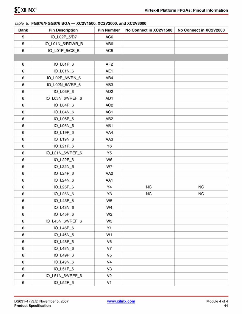
Virtex-II Platform FPGAs: Pinout InformationR
DS031-4 (v3.5) November 5, 2007 www.xilinx.com Module 4 of 4Product Specification 44
5 IO_L02P_5/D7 AC6
5 IO_L01N_5/RDWR_B AB6
5 IO_L01P_5/CS_B AC5
6 IO_L01P_6 AF2
6 IO_L01N_6 AE1
6 IO_L02P_6/VRN_6 AB4
6 IO_L02N_6/VRP_6 AB3
6 IO_L03P_6 AD2
6 IO_L03N_6/VREF_6 AD1
6 IO_L04P_6 AC2
6 IO_L04N_6 AC1
6 IO_L06P_6 AB2
6 IO_L06N_6 AB1
6 IO_L19P_6 AA4
6 IO_L19N_6 AA3
6 IO_L21P_6 Y6
6 IO_L21N_6/VREF_6 Y5
6 IO_L22P_6 W6
6 IO_L22N_6 W7
6 IO_L24P_6 AA2
6 IO_L24N_6 AA1
6 IO_L25P_6 Y4 NC NC
6 IO_L25N_6 Y3 NC NC
6 IO_L43P_6 W5
6 IO_L43N_6 W4
6 IO_L45P_6 W2
6 IO_L45N_6/VREF_6 W3
6 IO_L46P_6 Y1
6 IO_L46N_6 W1
6 IO_L48P_6 V6
6 IO_L48N_6 V7
6 IO_L49P_6 V5
6 IO_L49N_6 V4
6 IO_L51P_6 V3
6 IO_L51N_6/VREF_6 V2
6 IO_L52P_6 V1
Table 8: FG676/FGG676 BGA — XC2V1500, XC2V2000, and XC2V3000
Bank Pin Description Pin Number No Connect in XC2V1500 No Connect in XC2V2000

Virtex-II Platform FPGAs: Pinout InformationR
DS031-4 (v3.5) November 5, 2007 www.xilinx.com Module 4 of 4Product Specification 45
6 IO_L52N_6 U1
6 IO_L54P_6 U7
6 IO_L54N_6 T7
6 IO_L67P_6 U4
6 IO_L67N_6 U3
6 IO_L69P_6 U6
6 IO_L69N_6/VREF_6 U5
6 IO_L70P_6 T5
6 IO_L70N_6 T6
6 IO_L72P_6 T8
6 IO_L72N_6 R8
6 IO_L73P_6 T2 NC
6 IO_L73N_6 T1 NC
6 IO_L75P_6 T4 NC
6 IO_L75N_6/VREF_6 T3 NC
6 IO_L76P_6 R6 NC
6 IO_L76N_6 R5 NC
6 IO_L78P_6 R4 NC
6 IO_L78N_6 R3 NC
6 IO_L91P_6 R2
6 IO_L91N_6 R1
6 IO_L93P_6 R7
6 IO_L93N_6/VREF_6 P7
6 IO_L94P_6 P6
6 IO_L94N_6 P5
6 IO_L96P_6 P4
6 IO_L96N_6 P3
7 IO_L96P_7 P1
7 IO_L96N_7 N1
7 IO_L94P_7 N4
7 IO_L94N_7 N5
7 IO_L93P_7/VREF_7 N6
7 IO_L93N_7 N7
7 IO_L91P_7 P8
7 IO_L91N_7 N8
7 IO_L78P_7 M1 NC
Table 8: FG676/FGG676 BGA — XC2V1500, XC2V2000, and XC2V3000
Bank Pin Description Pin Number No Connect in XC2V1500 No Connect in XC2V2000

Virtex-II Platform FPGAs: Pinout InformationR
DS031-4 (v3.5) November 5, 2007 www.xilinx.com Module 4 of 4Product Specification 46
7 IO_L78N_7 M2 NC
7 IO_L76P_7 M5 NC
7 IO_L76N_7 M6 NC
7 IO_L75P_7/VREF_7 M3 NC
7 IO_L75N_7 M4 NC
7 IO_L73P_7 M7 NC
7 IO_L73N_7 M8 NC
7 IO_L72P_7 L1
7 IO_L72N_7 L2
7 IO_L70P_7 L5
7 IO_L70N_7 L6
7 IO_L69P_7/VREF_7 L3
7 IO_L69N_7 L4
7 IO_L67P_7 K1
7 IO_L67N_7 J1
7 IO_L54P_7 K3
7 IO_L54N_7 K4
7 IO_L52P_7 K5
7 IO_L52N_7 K6
7 IO_L51P_7/VREF_7 L8
7 IO_L51N_7 L7
7 IO_L49P_7 J2
7 IO_L49N_7 H1
7 IO_L48P_7 J3
7 IO_L48N_7 J4
7 IO_L46P_7 J5
7 IO_L46N_7 J6
7 IO_L45P_7/VREF_7 H5
7 IO_L45N_7 H4
7 IO_L43P_7 K7
7 IO_L43N_7 J7
7 IO_L25P_7 H2 NC NC
7 IO_L25N_7 H3 NC NC
7 IO_L24P_7 G1
7 IO_L24N_7 F1
7 IO_L22P_7 G3
7 IO_L22N_7 G4
Table 8: FG676/FGG676 BGA — XC2V1500, XC2V2000, and XC2V3000
Bank Pin Description Pin Number No Connect in XC2V1500 No Connect in XC2V2000

Virtex-II Platform FPGAs: Pinout InformationR
DS031-4 (v3.5) November 5, 2007 www.xilinx.com Module 4 of 4Product Specification 47
7 IO_L21P_7/VREF_7 F3
7 IO_L21N_7 F2
7 IO_L19P_7 H6
7 IO_L19N_7 H7
7 IO_L06P_7 E1
7 IO_L06N_7 E2
7 IO_L04P_7 D1
7 IO_L04N_7 D2
7 IO_L03P_7/VREF_7 C1
7 IO_L03N_7 C2
7 IO_L02P_7/VRN_7 E3
7 IO_L02N_7/VRP_7 E4
7 IO_L01P_7 G5
7 IO_L01N_7 F4
0 VCCO_0 J13
0 VCCO_0 J12
0 VCCO_0 J11
0 VCCO_0 H10
0 VCCO_0 H9
0 VCCO_0 B10
0 VCCO_0 B7
1 VCCO_1 B17
1 VCCO_1 J16
1 VCCO_1 J15
1 VCCO_1 J14
1 VCCO_1 H18
1 VCCO_1 H17
1 VCCO_1 B20
2 VCCO_2 N18
2 VCCO_2 M18
2 VCCO_2 L18
2 VCCO_2 K25
2 VCCO_2 K19
2 VCCO_2 J19
2 VCCO_2 G25
3 VCCO_3 Y25
Table 8: FG676/FGG676 BGA — XC2V1500, XC2V2000, and XC2V3000
Bank Pin Description Pin Number No Connect in XC2V1500 No Connect in XC2V2000

Virtex-II Platform FPGAs: Pinout InformationR
DS031-4 (v3.5) November 5, 2007 www.xilinx.com Module 4 of 4Product Specification 48
3 VCCO_3 V19
3 VCCO_3 U25
3 VCCO_3 U19
3 VCCO_3 T18
3 VCCO_3 R18
3 VCCO_3 P18
4 VCCO_4 AE20
4 VCCO_4 AE17
4 VCCO_4 W18
4 VCCO_4 W17
4 VCCO_4 V16
4 VCCO_4 V15
4 VCCO_4 V14
5 VCCO_5 AE10
5 VCCO_5 AE7
5 VCCO_5 W10
5 VCCO_5 W9
5 VCCO_5 V13
5 VCCO_5 V12
5 VCCO_5 V11
6 VCCO_6 Y2
6 VCCO_6 V8
6 VCCO_6 U8
6 VCCO_6 U2
6 VCCO_6 T9
6 VCCO_6 R9
6 VCCO_6 P9
7 VCCO_7 N9
7 VCCO_7 M9
7 VCCO_7 L9
7 VCCO_7 K8
7 VCCO_7 K2
7 VCCO_7 J8
7 VCCO_7 G2
NA CCLK AB21
NA PROG_B C4
Table 8: FG676/FGG676 BGA — XC2V1500, XC2V2000, and XC2V3000
Bank Pin Description Pin Number No Connect in XC2V1500 No Connect in XC2V2000

Virtex-II Platform FPGAs: Pinout InformationR
DS031-4 (v3.5) November 5, 2007 www.xilinx.com Module 4 of 4Product Specification 49
NA DONE AD22
NA M0 AD4
NA M1 AA5
NA M2 AD5
NA HSWAP_EN D5
NA TCK E21
NA TDI F5
NA TDO F22
NA TMS D22
NA PWRDWN_B AD23
NA DXN F7
NA DXP C5
NA VBATT C23
NA RSVD C22
NA VCCAUX AD13
NA VCCAUX AC24
NA VCCAUX AC3
NA VCCAUX P24
NA VCCAUX N3
NA VCCAUX D24
NA VCCAUX D3
NA VCCAUX C14
NA VCCINT W19
NA VCCINT W8
NA VCCINT V18
NA VCCINT V17
NA VCCINT V10
NA VCCINT V9
NA VCCINT U18
NA VCCINT U9
NA VCCINT K18
NA VCCINT K9
NA VCCINT J18
NA VCCINT J17
NA VCCINT J10
NA VCCINT J9
Table 8: FG676/FGG676 BGA — XC2V1500, XC2V2000, and XC2V3000
Bank Pin Description Pin Number No Connect in XC2V1500 No Connect in XC2V2000

Virtex-II Platform FPGAs: Pinout InformationR
DS031-4 (v3.5) November 5, 2007 www.xilinx.com Module 4 of 4Product Specification 50
NA VCCINT H19
NA VCCINT H8
NA GND AF26
NA GND AF1
NA GND AE25
NA GND AE14
NA GND AE13
NA GND AE2
NA GND AD24
NA GND AD3
NA GND AC23
NA GND AC4
NA GND AB22
NA GND AB5
NA GND AA21
NA GND AA6
NA GND U17
NA GND U16
NA GND U15
NA GND U14
NA GND U13
NA GND U12
NA GND U11
NA GND U10
NA GND T17
NA GND T16
NA GND T15
NA GND T14
NA GND T13
NA GND T12
NA GND T11
NA GND T10
NA GND R17
NA GND R16
NA GND R15
NA GND R14
NA GND R13
Table 8: FG676/FGG676 BGA — XC2V1500, XC2V2000, and XC2V3000
Bank Pin Description Pin Number No Connect in XC2V1500 No Connect in XC2V2000

Virtex-II Platform FPGAs: Pinout InformationR
DS031-4 (v3.5) November 5, 2007 www.xilinx.com Module 4 of 4Product Specification 51
NA GND R12
NA GND R11
NA GND R10
NA GND P25
NA GND P17
NA GND P16
NA GND P15
NA GND P14
NA GND P13
NA GND P12
NA GND P11
NA GND P10
NA GND P2
NA GND N25
NA GND N17
NA GND N16
NA GND N15
NA GND N14
NA GND N13
NA GND N12
NA GND N11
NA GND N10
NA GND N2
NA GND M17
NA GND M16
NA GND M15
NA GND M14
NA GND M13
NA GND M12
NA GND M11
NA GND M10
NA GND L17
NA GND L16
NA GND L15
NA GND L14
NA GND L13
NA GND L12
Table 8: FG676/FGG676 BGA — XC2V1500, XC2V2000, and XC2V3000
Bank Pin Description Pin Number No Connect in XC2V1500 No Connect in XC2V2000
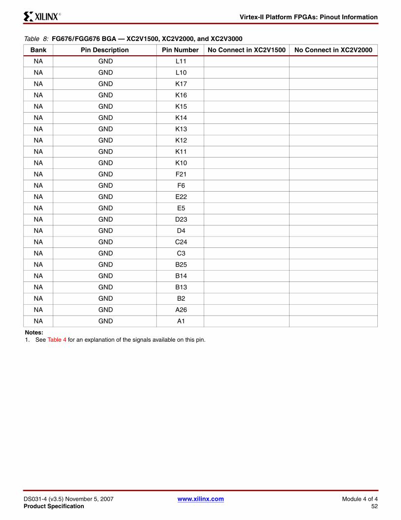
Virtex-II Platform FPGAs: Pinout InformationR
DS031-4 (v3.5) November 5, 2007 www.xilinx.com Module 4 of 4Product Specification 52
NA GND L11
NA GND L10
NA GND K17
NA GND K16
NA GND K15
NA GND K14
NA GND K13
NA GND K12
NA GND K11
NA GND K10
NA GND F21
NA GND F6
NA GND E22
NA GND E5
NA GND D23
NA GND D4
NA GND C24
NA GND C3
NA GND B25
NA GND B14
NA GND B13
NA GND B2
NA GND A26
NA GND A1
Notes: 1. See Table 4 for an explanation of the signals available on this pin.
Table 8: FG676/FGG676 BGA — XC2V1500, XC2V2000, and XC2V3000
Bank Pin Description Pin Number No Connect in XC2V1500 No Connect in XC2V2000

Virtex-II Platform FPGAs: Pinout InformationR
DS031-4 (v3.5) November 5, 2007 www.xilinx.com Module 4 of 4Product Specification 53
FG676/FGG676 Fine-Pitch BGA Package Specifications (1.00mm pitch)
Figure 4: FG676/FGG676 Fine-Pitch BGA Package Specifications

Virtex-II Platform FPGAs: Pinout InformationR
DS031-4 (v3.5) November 5, 2007 www.xilinx.com Module 4 of 4Product Specification 54
BG575/BGG575 Standard BGA PackageAs shown in Table 9, XC2V1000, XC2V1500, and XC2V2000 Virtex-II devices are available in the BG575/BGG575 BGApackage. Pins in the XC2V1000, XC2V1500, and XC2V2000 devices are the same, except for the pin differences in theXC2V1000 and XC2V1500 devices shown in the No Connect columns. Following this table are the BG575/BGG575Standard BGA Package Specifications (1.27mm pitch).
Table 9: BG575/BGG575 BGA — XC2V1000, XC2V1500, and XC2V2000
Bank Pin Description Pin Number No Connect in XC2V1000 No Connect in XC2V1500
0 IO_L01N_0 A3
0 IO_L01P_0 A4
0 IO_L02N_0 D5
0 IO_L02P_0 C5
0 IO_L03N_0/VRP_0 E6
0 IO_L03P_0/VRN_0 D6
0 IO_L04N_0/VREF_0 F7
0 IO_L04P_0 E7
0 IO_L05N_0 G8
0 IO_L05P_0 H9
0 IO_L06N_0 A5
0 IO_L06P_0 A6
0 IO_L19N_0 B5
0 IO_L19P_0 B6
0 IO_L21N_0 D7
0 IO_L21P_0/VREF_0 C7
0 IO_L22N_0 F8
0 IO_L22P_0 E8
0 IO_L24N_0 G9
0 IO_L24P_0 F9
0 IO_L49N_0 G10
0 IO_L49P_0 H10
0 IO_L51N_0 B7
0 IO_L51P_0/VREF_0 B8
0 IO_L52N_0 D8
0 IO_L52P_0 C8
0 IO_L54N_0 E9
0 IO_L54P_0 D9
0 IO_L67N_0 A8 NC
0 IO_L67P_0 A9 NC
0 IO_L69N_0 C9 NC

Virtex-II Platform FPGAs: Pinout InformationR
DS031-4 (v3.5) November 5, 2007 www.xilinx.com Module 4 of 4Product Specification 55
0 IO_L69P_0/VREF_0 B9 NC
0 IO_L70N_0 F10 NC
0 IO_L70P_0 E10 NC
0 IO_L72N_0 A10 NC
0 IO_L72P_0 A11 NC
0 IO_L73N_0 C10 NC NC
0 IO_L73P_0 B10 NC NC
0 IO_L91N_0/VREF_0 D11
0 IO_L91P_0 C11
0 IO_L92N_0 G11
0 IO_L92P_0 E11
0 IO_L93N_0 C12
0 IO_L93P_0 B12
0 IO_L94N_0/VREF_0 E12
0 IO_L94P_0 D12
0 IO_L95N_0/GCLK7P G12
0 IO_L95P_0/GCLK6S F12
0 IO_L96N_0/GCLK5P H11
0 IO_L96P_0/GCLK4S H12
1 IO_L96N_1/GCLK3P A13
1 IO_L96P_1/GCLK2S A14
1 IO_L95N_1/GCLK1P B13
1 IO_L95P_1/GCLK0S C13
1 IO_L94N_1 D13
1 IO_L94P_1/VREF_1 E13
1 IO_L93N_1 F13
1 IO_L93P_1 G13
1 IO_L92N_1 H13
1 IO_L92P_1 H14
1 IO_L91N_1 C14
1 IO_L91P_1/VREF_1 D14
1 IO_L73N_1 E14 NC NC
1 IO_L73P_1 G14 NC NC
1 IO_L72N_1 A15 NC
1 IO_L72P_1 A16 NC
Table 9: BG575/BGG575 BGA — XC2V1000, XC2V1500, and XC2V2000
Bank Pin Description Pin Number No Connect in XC2V1000 No Connect in XC2V1500

Virtex-II Platform FPGAs: Pinout InformationR
DS031-4 (v3.5) November 5, 2007 www.xilinx.com Module 4 of 4Product Specification 56
1 IO_L70N_1 B15 NC
1 IO_L70P_1 C15 NC
1 IO_L69N_1/VREF_1 E15 NC
1 IO_L69P_1 F15 NC
1 IO_L67N_1 G15 NC
1 IO_L67P_1 H15 NC
1 IO_L54N_1 B16
1 IO_L54P_1 C16
1 IO_L52N_1 D16
1 IO_L52P_1 E16
1 IO_L51N_1/VREF_1 F16
1 IO_L51P_1 G16
1 IO_L49N_1 A17
1 IO_L49P_1 A19
1 IO_L24N_1 B17
1 IO_L24P_1 B18
1 IO_L22N_1 C17
1 IO_L22P_1 D17
1 IO_L21N_1/VREF_1 F17
1 IO_L21P_1 E17
1 IO_L19N_1 A20
1 IO_L19P_1 A21
1 IO_L06N_1 B19
1 IO_L06P_1 B20
1 IO_L05N_1 C18
1 IO_L05P_1 D18
1 IO_L04N_1 C20
1 IO_L04P_1/VREF_1 D20
1 IO_L03N_1/VRP_1 D19
1 IO_L03P_1/VRN_1 E19
1 IO_L02N_1 E18
1 IO_L02P_1 F18
1 IO_L01N_1 H16
1 IO_L01P_1 G17
2 IO_L01N_2 D22
Table 9: BG575/BGG575 BGA — XC2V1000, XC2V1500, and XC2V2000
Bank Pin Description Pin Number No Connect in XC2V1000 No Connect in XC2V1500

Virtex-II Platform FPGAs: Pinout InformationR
DS031-4 (v3.5) November 5, 2007 www.xilinx.com Module 4 of 4Product Specification 57
2 IO_L01P_2 D23
2 IO_L02N_2/VRP_2 E21
2 IO_L02P_2/VRN_2 E22
2 IO_L03N_2 F21
2 IO_L03P_2/VREF_2 F20
2 IO_L04N_2 G20
2 IO_L04P_2 G19
2 IO_L06N_2 H18
2 IO_L06P_2 J17
2 IO_L19N_2 D24
2 IO_L19P_2 E23
2 IO_L21N_2 E24
2 IO_L21P_2/VREF_2 F24
2 IO_L22N_2 F23
2 IO_L22P_2 G23
2 IO_L24N_2 G21
2 IO_L24P_2 G22
2 IO_L43N_2 H19
2 IO_L43P_2 H20
2 IO_L45N_2 J18
2 IO_L45P_2/VREF_2 J19
2 IO_L46N_2 K17
2 IO_L46P_2 K18
2 IO_L48N_2 H23
2 IO_L48P_2 H24
2 IO_L49N_2 H21
2 IO_L49P_2 H22
2 IO_L51N_2 J24
2 IO_L51P_2/VREF_2 K24
2 IO_L52N_2 J22
2 IO_L52P_2 J23
2 IO_L54N_2 J20
2 IO_L54P_2 J21
2 IO_L67N_2 K19 NC
2 IO_L67P_2 K20 NC
2 IO_L69N_2 L17 NC
Table 9: BG575/BGG575 BGA — XC2V1000, XC2V1500, and XC2V2000
Bank Pin Description Pin Number No Connect in XC2V1000 No Connect in XC2V1500

Virtex-II Platform FPGAs: Pinout InformationR
DS031-4 (v3.5) November 5, 2007 www.xilinx.com Module 4 of 4Product Specification 58
2 IO_L69P_2/VREF_2 L18 NC
2 IO_L70N_2 K23 NC
2 IO_L70P_2 L24 NC
2 IO_L72N_2 K22 NC
2 IO_L72P_2 L22 NC
2 IO_L73N_2 L21 NC NC
2 IO_L73P_2 L20 NC NC
2 IO_L91N_2 M23
2 IO_L91P_2 N24
2 IO_L93N_2 M21
2 IO_L93P_2/VREF_2 M22
2 IO_L94N_2 M19
2 IO_L94P_2 M20
2 IO_L96N_2 M17
2 IO_L96P_2 M18
3 IO_L96N_3 N23
3 IO_L96P_3 N22
3 IO_L94N_3 N20
3 IO_L94P_3 N21
3 IO_L93N_3/VREF_3 N19
3 IO_L93P_3 N18
3 IO_L91N_3 N17
3 IO_L91P_3 P17
3 IO_L73N_3 P24 NC NC
3 IO_L73P_3 R24 NC NC
3 IO_L72N_3 R23 NC
3 IO_L72P_3 R22 NC
3 IO_L70N_3 P22 NC
3 IO_L70P_3 P21 NC
3 IO_L69N_3/VREF_3 P20 NC
3 IO_L69P_3 P18 NC
3 IO_L67N_3 T24 NC
3 IO_L67P_3 U24 NC
3 IO_L54N_3 T23
3 IO_L54P_3 T22
Table 9: BG575/BGG575 BGA — XC2V1000, XC2V1500, and XC2V2000
Bank Pin Description Pin Number No Connect in XC2V1000 No Connect in XC2V1500

Virtex-II Platform FPGAs: Pinout InformationR
DS031-4 (v3.5) November 5, 2007 www.xilinx.com Module 4 of 4Product Specification 59
3 IO_L52N_3 T21
3 IO_L52P_3 T20
3 IO_L51N_3/VREF_3 R20
3 IO_L51P_3 R19
3 IO_L49N_3 W24
3 IO_L49P_3 W23
3 IO_L48N_3 U23
3 IO_L48P_3 V23
3 IO_L46N_3 U22
3 IO_L46P_3 U21
3 IO_L45N_3/VREF_3 V22
3 IO_L45P_3 V21
3 IO_L43N_3 U19
3 IO_L43P_3 U20
3 IO_L24N_3 T19
3 IO_L24P_3 T18
3 IO_L22N_3 R18
3 IO_L22P_3 R17
3 IO_L21N_3/VREF_3 Y24
3 IO_L21P_3 Y23
3 IO_L19N_3 AA24
3 IO_L19P_3 AB24
3 IO_L06N_3 AA23
3 IO_L06P_3 AA22
3 IO_L04N_3 Y22
3 IO_L04P_3 Y21
3 IO_L03N_3/VREF_3 W21
3 IO_L03P_3 W20
3 IO_L02N_3/VRP_3 V20
3 IO_L02P_3/VRN_3 V19
3 IO_L01N_3 U18
3 IO_L01P_3 T17
4 IO_L01N_4/BUSY/DOUT(1) AD22
4 IO_L01P_4/INIT_B AD21
4 IO_L02N_4/D0/DIN(1) AA20
Table 9: BG575/BGG575 BGA — XC2V1000, XC2V1500, and XC2V2000
Bank Pin Description Pin Number No Connect in XC2V1000 No Connect in XC2V1500

Virtex-II Platform FPGAs: Pinout InformationR
DS031-4 (v3.5) November 5, 2007 www.xilinx.com Module 4 of 4Product Specification 60
4 IO_L02P_4/D1 AB20
4 IO_L03N_4/D2/ALT_VRP_4 Y19
4 IO_L03P_4/D3/ALT_VRN_4 AA19
4 IO_L04N_4/VREF_4 W18
4 IO_L04P_4 Y18
4 IO_L05N_4/VRP_4 U16
4 IO_L05P_4/VRN_4 V17
4 IO_L06N_4 AD20
4 IO_L06P_4 AD19
4 IO_L19N_4 AC20
4 IO_L19P_4 AC19
4 IO_L21N_4 AA18
4 IO_L21P_4/VREF_4 AB18
4 IO_L22N_4 AC18
4 IO_L22P_4 AC17
4 IO_L24N_4 AA17
4 IO_L24P_4 AB17
4 IO_L49N_4 Y17
4 IO_L49P_4 W17
4 IO_L51N_4 V16
4 IO_L51P_4/VREF_4 W16
4 IO_L52N_4 AD17
4 IO_L52P_4 AD16
4 IO_L54N_4 AB16
4 IO_L54P_4 AC16
4 IO_L67N_4 Y16 NC
4 IO_L67P_4 AA16 NC
4 IO_L69N_4 W15 NC
4 IO_L69P_4/VREF_4 Y15 NC
4 IO_L70N_4 U15 NC
4 IO_L70P_4 V15 NC
4 IO_L72N_4 AD15 NC
4 IO_L72P_4 AD14 NC
4 IO_L73N_4 AB15 NC NC
4 IO_L73P_4 AC15 NC NC
4 IO_L91N_4/VREF_4 AA14
Table 9: BG575/BGG575 BGA — XC2V1000, XC2V1500, and XC2V2000
Bank Pin Description Pin Number No Connect in XC2V1000 No Connect in XC2V1500

Virtex-II Platform FPGAs: Pinout InformationR
DS031-4 (v3.5) November 5, 2007 www.xilinx.com Module 4 of 4Product Specification 61
4 IO_L91P_4 AB14
4 IO_L92N_4 V14
4 IO_L92P_4 Y14
4 IO_L93N_4 AB13
4 IO_L93P_4 AC13
4 IO_L94N_4/VREF_4 Y13
4 IO_L94P_4 AA13
4 IO_L95N_4/GCLK3S V13
4 IO_L95P_4/GCLK2P W13
4 IO_L96N_4/GCLK1S U14
4 IO_L96P_4/GCLK0P U13
5 IO_L96N_5/GCLK7S AD12
5 IO_L96P_5/GCLK6P AD11
5 IO_L95N_5/GCLK5S AC12
5 IO_L95P_5/GCLK4P AB12
5 IO_L94N_5 AA12
5 IO_L94P_5/VREF_5 Y12
5 IO_L93N_5 W12
5 IO_L93P_5 V12
5 IO_L92N_5 U12
5 IO_L92P_5 U11
5 IO_L91N_5 AB11
5 IO_L91P_5/VREF_5 AA11
5 IO_L73N_5 Y11 NC NC
5 IO_L73P_5 V11 NC NC
5 IO_L72N_5 AD10 NC
5 IO_L72P_5 AD9 NC
5 IO_L70N_5 AC10 NC
5 IO_L70P_5 AB10 NC
5 IO_L69N_5/VREF_5 Y10 NC
5 IO_L69P_5 W10 NC
5 IO_L67N_5 V10 NC
5 IO_L67P_5 U10 NC
5 IO_L54N_5 AC9
5 IO_L54P_5 AB9
Table 9: BG575/BGG575 BGA — XC2V1000, XC2V1500, and XC2V2000
Bank Pin Description Pin Number No Connect in XC2V1000 No Connect in XC2V1500

Virtex-II Platform FPGAs: Pinout InformationR
DS031-4 (v3.5) November 5, 2007 www.xilinx.com Module 4 of 4Product Specification 62
5 IO_L52N_5 AA9
5 IO_L52P_5 Y9
5 IO_L51N_5/VREF_5 W9
5 IO_L51P_5 V9
5 IO_L49N_5 AD8
5 IO_L49P_5 AD6
5 IO_L24N_5 AC8
5 IO_L24P_5 AC7
5 IO_L22N_5 AB8
5 IO_L22P_5 AA8
5 IO_L21N_5/VREF_5 W8
5 IO_L21P_5 Y8
5 IO_L19N_5 AD5
5 IO_L19P_5 AD4
5 IO_L06N_5 AC6
5 IO_L06P_5 AC5
5 IO_L05N_5/VRP_5 AB7
5 IO_L05P_5/VRN_5 AA7
5 IO_L04N_5 AB5
5 IO_L04P_5/VREF_5 AA5
5 IO_L03N_5/D4/ALT_VRP_5 AA6
5 IO_L03P_5/D5/ALT_VRN_5 Y6
5 IO_L02N_5/D6 Y7
5 IO_L02P_5/D7 W7
5 IO_L01N_5/RDWR_B V8
5 IO_L01P_5/CS_B U9
6 IO_L01P_6 AB2
6 IO_L01N_6 AB1
6 IO_L02P_6/VRN_6 AA3
6 IO_L02N_6/VRP_6 AA2
6 IO_L03P_6 Y4
6 IO_L03N_6/VREF_6 Y3
6 IO_L04P_6 W4
6 IO_L04N_6 W5
6 IO_L06P_6 V5
Table 9: BG575/BGG575 BGA — XC2V1000, XC2V1500, and XC2V2000
Bank Pin Description Pin Number No Connect in XC2V1000 No Connect in XC2V1500

Virtex-II Platform FPGAs: Pinout InformationR
DS031-4 (v3.5) November 5, 2007 www.xilinx.com Module 4 of 4Product Specification 63
6 IO_L06N_6 V6
6 IO_L19P_6 U7
6 IO_L19N_6 T8
6 IO_L21P_6 AA1
6 IO_L21N_6/VREF_6 Y2
6 IO_L22P_6 Y1
6 IO_L22N_6 W1
6 IO_L24P_6 W2
6 IO_L24N_6 V2
6 IO_L43P_6 V4
6 IO_L43N_6 V3
6 IO_L45P_6 U6
6 IO_L45N_6/VREF_6 U5
6 IO_L46P_6 T7
6 IO_L46N_6 T6
6 IO_L48P_6 R8
6 IO_L48N_6 R7
6 IO_L49P_6 U2
6 IO_L49N_6 U1
6 IO_L51P_6 U4
6 IO_L51N_6/VREF_6 U3
6 IO_L52P_6 T1
6 IO_L52N_6 R1
6 IO_L54P_6 T3
6 IO_L54N_6 T2
6 IO_L67P_6 T5 NC
6 IO_L67N_6 T4 NC
6 IO_L69P_6 R6 NC
6 IO_L69N_6/VREF_6 R5 NC
6 IO_L70P_6 P8 NC
6 IO_L70N_6 P7 NC
6 IO_L72P_6 R2 NC
6 IO_L72N_6 P1 NC
6 IO_L73P_6 R3 NC NC
6 IO_L73N_6 P3 NC NC
6 IO_L91P_6 P5
Table 9: BG575/BGG575 BGA — XC2V1000, XC2V1500, and XC2V2000
Bank Pin Description Pin Number No Connect in XC2V1000 No Connect in XC2V1500

Virtex-II Platform FPGAs: Pinout InformationR
DS031-4 (v3.5) November 5, 2007 www.xilinx.com Module 4 of 4Product Specification 64
6 IO_L91N_6 P4
6 IO_L93P_6 N4
6 IO_L93N_6/VREF_6 N3
6 IO_L94P_6 N6
6 IO_L94N_6 N5
6 IO_L96P_6 N8
6 IO_L96N_6 N7
7 IO_L96P_7 N2
7 IO_L96N_7 M1
7 IO_L94P_7 M2
7 IO_L94N_7 M3
7 IO_L93P_7/VREF_7 M4
7 IO_L93N_7 M5
7 IO_L91P_7 M6
7 IO_L91N_7 M7
7 IO_L73P_7 M8 NC NC
7 IO_L73N_7 L8 NC NC
7 IO_L72P_7 L1 NC
7 IO_L72N_7 K1 NC
7 IO_L70P_7 K2 NC
7 IO_L70N_7 K3 NC
7 IO_L69P_7/VREF_7 L3 NC
7 IO_L69N_7 L4 NC
7 IO_L67P_7 L5 NC
7 IO_L67N_7 L7 NC
7 IO_L54P_7 J1
7 IO_L54N_7 H1
7 IO_L52P_7 J2
7 IO_L52N_7 J3
7 IO_L51P_7/VREF_7 J4
7 IO_L51N_7 J5
7 IO_L49P_7 K5
7 IO_L49N_7 K6
7 IO_L48P_7 F1
7 IO_L48N_7 F2
Table 9: BG575/BGG575 BGA — XC2V1000, XC2V1500, and XC2V2000
Bank Pin Description Pin Number No Connect in XC2V1000 No Connect in XC2V1500

Virtex-II Platform FPGAs: Pinout InformationR
DS031-4 (v3.5) November 5, 2007 www.xilinx.com Module 4 of 4Product Specification 65
7 IO_L46P_7 H2
7 IO_L46N_7 G2
7 IO_L45P_7/VREF_7 H3
7 IO_L45N_7 H4
7 IO_L43P_7 G3
7 IO_L43N_7 G4
7 IO_L24P_7 H5
7 IO_L24N_7 H6
7 IO_L22P_7 J6
7 IO_L22N_7 J7
7 IO_L21P_7/VREF_7 K7
7 IO_L21N_7 K8
7 IO_L19P_7 E1
7 IO_L19N_7 E2
7 IO_L06P_7 D2
7 IO_L06N_7 D3
7 IO_L04P_7 E3
7 IO_L04N_7 E4
7 IO_L03P_7/VREF_7 F4
7 IO_L03N_7 F5
7 IO_L02P_7/VRN_7 G5
7 IO_L02N_7/VRP_7 G6
7 IO_L01P_7 H7
7 IO_L01N_7 J8
0 VCCO_0 J12
0 VCCO_0 J11
0 VCCO_0 J10
0 VCCO_0 F11
0 VCCO_0 C6
0 VCCO_0 B11
1 VCCO_1 J15
1 VCCO_1 J14
1 VCCO_1 J13
1 VCCO_1 F14
1 VCCO_1 C19
Table 9: BG575/BGG575 BGA — XC2V1000, XC2V1500, and XC2V2000
Bank Pin Description Pin Number No Connect in XC2V1000 No Connect in XC2V1500

Virtex-II Platform FPGAs: Pinout InformationR
DS031-4 (v3.5) November 5, 2007 www.xilinx.com Module 4 of 4Product Specification 66
1 VCCO_1 B14
2 VCCO_2 M16
2 VCCO_2 L23
2 VCCO_2 L19
2 VCCO_2 L16
2 VCCO_2 K16
2 VCCO_2 F22
3 VCCO_3 W22
3 VCCO_3 R16
3 VCCO_3 P23
3 VCCO_3 P19
3 VCCO_3 P16
3 VCCO_3 N16
4 VCCO_4 AC14
4 VCCO_4 AB19
4 VCCO_4 W14
4 VCCO_4 T15
4 VCCO_4 T14
4 VCCO_4 T13
5 VCCO_5 AC11
5 VCCO_5 AB6
5 VCCO_5 W11
5 VCCO_5 T12
5 VCCO_5 T11
5 VCCO_5 T10
6 VCCO_6 W3
6 VCCO_6 R9
6 VCCO_6 P9
6 VCCO_6 P6
6 VCCO_6 P2
6 VCCO_6 N9
7 VCCO_7 M9
7 VCCO_7 L9
7 VCCO_7 L6
7 VCCO_7 L2
7 VCCO_7 K9
Table 9: BG575/BGG575 BGA — XC2V1000, XC2V1500, and XC2V2000
Bank Pin Description Pin Number No Connect in XC2V1000 No Connect in XC2V1500

Virtex-II Platform FPGAs: Pinout InformationR
DS031-4 (v3.5) November 5, 2007 www.xilinx.com Module 4 of 4Product Specification 67
7 VCCO_7 F3
NA CCLK AB23
NA PROG_B C1
NA DONE AB21
NA M0 AC4
NA M1 AB4
NA M2 AD3
NA HSWAP_EN C2
NA TCK C23
NA TDI D1
NA TDO C24
NA TMS C21
NA PWRDWN_B AC21
NA DXN B4
NA DXP C4
NA VBATT B21
NA RSVD A22
NA VCCAUX AD13
NA VCCAUX AC22
NA VCCAUX AC3
NA VCCAUX N1
NA VCCAUX M24
NA VCCAUX B22
NA VCCAUX B3
NA VCCAUX A12
NA VCCINT U17
NA VCCINT U8
NA VCCINT T16
NA VCCINT T9
NA VCCINT R15
NA VCCINT R14
NA VCCINT R13
NA VCCINT R12
NA VCCINT R11
Table 9: BG575/BGG575 BGA — XC2V1000, XC2V1500, and XC2V2000
Bank Pin Description Pin Number No Connect in XC2V1000 No Connect in XC2V1500

Virtex-II Platform FPGAs: Pinout InformationR
DS031-4 (v3.5) November 5, 2007 www.xilinx.com Module 4 of 4Product Specification 68
NA VCCINT R10
NA VCCINT P15
NA VCCINT P10
NA VCCINT N15
NA VCCINT N10
NA VCCINT M15
NA VCCINT M10
NA VCCINT L15
NA VCCINT L10
NA VCCINT K15
NA VCCINT K14
NA VCCINT K13
NA VCCINT K12
NA VCCINT K11
NA VCCINT K10
NA VCCINT J16
NA VCCINT J9
NA VCCINT H17
NA VCCINT H8
NA GND AD24
NA GND AD23
NA GND AD18
NA GND AD7
NA GND AD2
NA GND AD1
NA GND AC24
NA GND AC23
NA GND AC2
NA GND AC1
NA GND AB22
NA GND AB3
NA GND AA21
NA GND AA15
NA GND AA10
NA GND AA4
NA GND Y20
Table 9: BG575/BGG575 BGA — XC2V1000, XC2V1500, and XC2V2000
Bank Pin Description Pin Number No Connect in XC2V1000 No Connect in XC2V1500

Virtex-II Platform FPGAs: Pinout InformationR
DS031-4 (v3.5) November 5, 2007 www.xilinx.com Module 4 of 4Product Specification 69
NA GND Y5
NA GND W19
NA GND W6
NA GND V24
NA GND V18
NA GND V7
NA GND V1
NA GND R21
NA GND R4
NA GND P14
NA GND P13
NA GND P12
NA GND P11
NA GND N14
NA GND N13
NA GND N12
NA GND N11
NA GND M14
NA GND M13
NA GND M12
NA GND M11
NA GND L14
NA GND L13
NA GND L12
NA GND L11
NA GND K21
NA GND K4
NA GND G24
NA GND G18
NA GND G7
NA GND G1
NA GND F19
NA GND F6
NA GND E20
NA GND E5
NA GND D21
Table 9: BG575/BGG575 BGA — XC2V1000, XC2V1500, and XC2V2000
Bank Pin Description Pin Number No Connect in XC2V1000 No Connect in XC2V1500

Virtex-II Platform FPGAs: Pinout InformationR
DS031-4 (v3.5) November 5, 2007 www.xilinx.com Module 4 of 4Product Specification 70
NA GND D15
NA GND D10
NA GND D4
NA GND C22
NA GND C3
NA GND B24
NA GND B23
NA GND B2
NA GND B1
NA GND A24
NA GND A23
NA GND A18
NA GND A7
NA GND A2
Notes: 1. See Table 4 for an explanation of the signals available on this pin.
Table 9: BG575/BGG575 BGA — XC2V1000, XC2V1500, and XC2V2000
Bank Pin Description Pin Number No Connect in XC2V1000 No Connect in XC2V1500

Virtex-II Platform FPGAs: Pinout InformationR
DS031-4 (v3.5) November 5, 2007 www.xilinx.com Module 4 of 4Product Specification 71
BG575/BGG575 Standard BGA Package Specifications (1.27mm pitch)
Figure 5: BG575/BGG575 Standard BGA Package Specifications

Virtex-II Platform FPGAs: Pinout InformationR
DS031-4 (v3.5) November 5, 2007 www.xilinx.com Module 4 of 4Product Specification 72
BG728/BGG728 Standard BGA PackageAs shown in Table 10, XC2V3000 Virtex-II devices are available in the BG728/BGG728 BGA package. Following this tableare the BG728/BGG728 Standard BGA Package Specifications (1.27mm pitch).
Table 10: BG728 BGA — XC2V3000
Bank Pin Description Pin Number
0 IO_L01N_0 B3
0 IO_L01P_0 A3
0 IO_L02N_0 B4
0 IO_L02P_0 A4
0 IO_L03N_0/VRP_0 C5
0 IO_L03P_0/VRN_0 C6
0 IO_L04N_0/VREF_0 B5
0 IO_L04P_0 A5
0 IO_L05N_0 E6
0 IO_L05P_0 D6
0 IO_L06N_0 B6
0 IO_L06P_0 A6
0 IO_L19N_0 E7
0 IO_L19P_0 D8
0 IO_L21N_0 F8
0 IO_L21P_0/VREF_0 E8
0 IO_L22N_0 C7
0 IO_L22P_0 C8
0 IO_L24N_0 B7
0 IO_L24P_0 A7
0 IO_L25N_0 H9
0 IO_L25P_0 J9
0 IO_L27N_0 F9
0 IO_L27P_0/VREF_0 G9
0 IO_L28N_0 E9
0 IO_L28P_0 D9
0 IO_L30N_0 C9
0 IO_L30P_0 B9
0 IO_L49N_0 A8
0 IO_L49P_0 A9
0 IO_L51N_0 G10
0 IO_L51P_0/VREF_0 H10
0 IO_L52N_0 F10

Virtex-II Platform FPGAs: Pinout InformationR
DS031-4 (v3.5) November 5, 2007 www.xilinx.com Module 4 of 4Product Specification 73
0 IO_L52P_0 E10
0 IO_L54N_0 D10
0 IO_L54P_0 C10
0 IO_L67N_0 B10
0 IO_L67P_0 A10
0 IO_L69N_0 G11
0 IO_L69P_0/VREF_0 H11
0 IO_L70N_0 F11
0 IO_L70P_0 F12
0 IO_L72N_0 D11
0 IO_L72P_0 C11
0 IO_L73N_0 B11
0 IO_L73P_0 A11
0 IO_L75N_0 H12
0 IO_L75P_0/VREF_0 J12
0 IO_L76N_0 E12
0 IO_L76P_0 D12
0 IO_L78N_0 B12
0 IO_L78P_0 A12
0 IO_L91N_0/VREF_0 J13
0 IO_L91P_0 H13
0 IO_L92N_0 G13
0 IO_L92P_0 F13
0 IO_L93N_0 E13
0 IO_L93P_0 D13
0 IO_L94N_0/VREF_0 B13
0 IO_L94P_0 A13
0 IO_L95N_0/GCLK7P C13
0 IO_L95P_0/GCLK6S C14
0 IO_L96N_0/GCLK5P F14
0 IO_L96P_0/GCLK4S E14
1 IO_L96N_1/GCLK3P G14
1 IO_L96P_1/GCLK2S H14
1 IO_L95N_1/GCLK1P A15
1 IO_L95P_1/GCLK0S B15
Table 10: BG728 BGA — XC2V3000
Bank Pin Description Pin Number

Virtex-II Platform FPGAs: Pinout InformationR
DS031-4 (v3.5) November 5, 2007 www.xilinx.com Module 4 of 4Product Specification 74
1 IO_L94N_1 C15
1 IO_L94P_1/VREF_1 D15
1 IO_L93N_1 E15
1 IO_L93P_1 F15
1 IO_L92N_1 G15
1 IO_L92P_1 H15
1 IO_L91N_1 J15
1 IO_L91P_1/VREF_1 J16
1 IO_L78N_1 A16
1 IO_L78P_1 B16
1 IO_L76N_1 D16
1 IO_L76P_1 E16
1 IO_L75N_1/VREF_1 F16
1 IO_L75P_1 F17
1 IO_L73N_1 H16
1 IO_L73P_1 H17
1 IO_L72N_1 A17
1 IO_L72P_1 B17
1 IO_L70N_1 C17
1 IO_L70P_1 D17
1 IO_L69N_1/VREF_1 G18
1 IO_L69P_1 G17
1 IO_L67N_1 A18
1 IO_L67P_1 B18
1 IO_L54N_1 C18
1 IO_L54P_1 D18
1 IO_L52N_1 E18
1 IO_L52P_1 F18
1 IO_L51N_1/VREF_1 H19
1 IO_L51P_1 H18
1 IO_L49N_1 A19
1 IO_L49P_1 A20
1 IO_L30N_1 B19
1 IO_L30P_1 C19
1 IO_L28N_1 D19
1 IO_L28P_1 E19
Table 10: BG728 BGA — XC2V3000
Bank Pin Description Pin Number

Virtex-II Platform FPGAs: Pinout InformationR
DS031-4 (v3.5) November 5, 2007 www.xilinx.com Module 4 of 4Product Specification 75
1 IO_L27N_1/VREF_1 F19
1 IO_L27P_1 G19
1 IO_L25N_1 J19
1 IO_L25P_1 J20
1 IO_L24N_1 C20
1 IO_L24P_1 C21
1 IO_L22N_1 D20
1 IO_L22P_1 E21
1 IO_L21N_1/VREF_1 E20
1 IO_L21P_1 F20
1 IO_L19N_1 A21
1 IO_L19P_1 B21
1 IO_L06N_1 A22
1 IO_L06P_1 B22
1 IO_L05N_1 C22
1 IO_L05P_1 C23
1 IO_L04N_1 D22
1 IO_L04P_1/VREF_1 E22
1 IO_L03N_1/VRP_1 A23
1 IO_L03P_1/VRN_1 B23
1 IO_L02N_1 A24
1 IO_L02P_1 B24
1 IO_L01N_1 A25
1 IO_L01P_1 B25
2 IO_L01N_2 C27
2 IO_L01P_2 D27
2 IO_L02N_2/VRP_2 D25
2 IO_L02P_2/VRN_2 D26
2 IO_L03N_2 E24
2 IO_L03P_2/VREF_2 E25
2 IO_L04N_2 E26
2 IO_L04P_2 E27
2 IO_L06N_2 F23
2 IO_L06P_2 F24
2 IO_L19N_2 F25
Table 10: BG728 BGA — XC2V3000
Bank Pin Description Pin Number

Virtex-II Platform FPGAs: Pinout InformationR
DS031-4 (v3.5) November 5, 2007 www.xilinx.com Module 4 of 4Product Specification 76
2 IO_L19P_2 F26
2 IO_L21N_2 F27
2 IO_L21P_2/VREF_2 G27
2 IO_L22N_2 G23
2 IO_L22P_2 H23
2 IO_L24N_2 G25
2 IO_L24P_2 G26
2 IO_L25N_2 H21
2 IO_L25P_2 J21
2 IO_L27N_2 H22
2 IO_L27P_2/VREF_2 J22
2 IO_L28N_2 H24
2 IO_L28P_2 H25
2 IO_L30N_2 H27
2 IO_L30P_2 J27
2 IO_L43N_2 J23
2 IO_L43P_2 J24
2 IO_L45N_2 J25
2 IO_L45P_2/VREF_2 J26
2 IO_L46N_2 K20
2 IO_L46P_2 K21
2 IO_L48N_2 K22
2 IO_L48P_2 K23
2 IO_L49N_2 K24
2 IO_L49P_2 K25
2 IO_L51N_2 K26
2 IO_L51P_2/VREF_2 K27
2 IO_L52N_2 L20
2 IO_L52P_2 M20
2 IO_L54N_2 L21
2 IO_L54P_2 L22
2 IO_L67N_2 L24
2 IO_L67P_2 L25
2 IO_L69N_2 L26
2 IO_L69P_2/VREF_2 L27
2 IO_L70N_2 M19
Table 10: BG728 BGA — XC2V3000
Bank Pin Description Pin Number

Virtex-II Platform FPGAs: Pinout InformationR
DS031-4 (v3.5) November 5, 2007 www.xilinx.com Module 4 of 4Product Specification 77
2 IO_L70P_2 N19
2 IO_L72N_2 M22
2 IO_L72P_2 M23
2 IO_L73N_2 M24
2 IO_L73P_2 N24
2 IO_L75N_2 M26
2 IO_L75P_2/VREF_2 M27
2 IO_L76N_2 N20
2 IO_L76P_2 N21
2 IO_L78N_2 N22
2 IO_L78P_2 N23
2 IO_L91N_2 N25
2 IO_L91P_2 P25
2 IO_L93N_2 N26
2 IO_L93P_2/VREF_2 N27
2 IO_L94N_2 P20
2 IO_L94P_2 P21
2 IO_L96N_2 P22
2 IO_L96P_2 P23
3 IO_L96N_3 R27
3 IO_L96P_3 R26
3 IO_L94N_3 R25
3 IO_L94P_3 R24
3 IO_L93N_3/VREF_3 R23
3 IO_L93P_3 T23
3 IO_L91N_3 R22
3 IO_L91P_3 R21
3 IO_L78N_3 R20
3 IO_L78P_3 R19
3 IO_L76N_3 T27
3 IO_L76P_3 T26
3 IO_L75N_3/VREF_3 T24
3 IO_L75P_3 U24
3 IO_L73N_3 T22
3 IO_L73P_3 U22
Table 10: BG728 BGA — XC2V3000
Bank Pin Description Pin Number

Virtex-II Platform FPGAs: Pinout InformationR
DS031-4 (v3.5) November 5, 2007 www.xilinx.com Module 4 of 4Product Specification 78
3 IO_L72N_3 T20
3 IO_L72P_3 T19
3 IO_L70N_3 U27
3 IO_L70P_3 U26
3 IO_L69N_3/VREF_3 U25
3 IO_L69P_3 V25
3 IO_L67N_3 U21
3 IO_L67P_3 U20
3 IO_L54N_3 V27
3 IO_L54P_3 V26
3 IO_L52N_3 V24
3 IO_L52P_3 V23
3 IO_L51N_3/VREF_3 V22
3 IO_L51P_3 W22
3 IO_L49N_3 V21
3 IO_L49P_3 V20
3 IO_L48N_3 W27
3 IO_L48P_3 Y27
3 IO_L46N_3 W26
3 IO_L46P_3 W25
3 IO_L45N_3/VREF_3 W24
3 IO_L45P_3 W23
3 IO_L43N_3 W21
3 IO_L43P_3 W20
3 IO_L28N_3 W19
3 IO_L28P_3 Y19
3 IO_L27N_3/VREF_3 Y25
3 IO_L27P_3 Y24
3 IO_L25N_3 Y23
3 IO_L25P_3 AA23
3 IO_L24N_3 Y22
3 IO_L24P_3 Y21
3 IO_L22N_3 AA27
3 IO_L22P_3 AB27
3 IO_L21N_3/VREF_3 AA26
3 IO_L21P_3 AA25
Table 10: BG728 BGA — XC2V3000
Bank Pin Description Pin Number

Virtex-II Platform FPGAs: Pinout InformationR
DS031-4 (v3.5) November 5, 2007 www.xilinx.com Module 4 of 4Product Specification 79
3 IO_L19N_3 AB26
3 IO_L19P_3 AB25
3 IO_L06N_3 AB24
3 IO_L06P_3 AB23
3 IO_L04N_3 AC27
3 IO_L04P_3 AC26
3 IO_L03N_3/VREF_3 AC25
3 IO_L03P_3 AC24
3 IO_L02N_3/VRP_3 AD27
3 IO_L02P_3/VRN_3 AE27
3 IO_L01N_3 AD26
3 IO_L01P_3 AD25
4 IO_L01N_4/BUSY/DOUT(1) AF25
4 IO_L01P_4/INIT_B AG25
4 IO_L02N_4/D0/DIN(1) AF24
4 IO_L02P_4/D1 AG24
4 IO_L03N_4/D2/ALT_VRP_4 AD23
4 IO_L03P_4/D3/ALT_VRN_4 AE23
4 IO_L04N_4/VREF_4 AF23
4 IO_L04P_4 AG23
4 IO_L05N_4/VRP_4 AD22
4 IO_L05P_4/VRN_4 AE22
4 IO_L06N_4 AF22
4 IO_L06P_4 AG22
4 IO_L19N_4 AC21
4 IO_L19P_4 AB21
4 IO_L21N_4 AE21
4 IO_L21P_4/VREF_4 AE20
4 IO_L22N_4 AF21
4 IO_L22P_4 AG21
4 IO_L24N_4 AB20
4 IO_L24P_4 AA20
4 IO_L25N_4 AC20
4 IO_L25P_4 AD20
4 IO_L27N_4 AG20
Table 10: BG728 BGA — XC2V3000
Bank Pin Description Pin Number

Virtex-II Platform FPGAs: Pinout InformationR
DS031-4 (v3.5) November 5, 2007 www.xilinx.com Module 4 of 4Product Specification 80
4 IO_L27P_4/VREF_4 AG19
4 IO_L28N_4 AB19
4 IO_L28P_4 AA19
4 IO_L30N_4 AC19
4 IO_L30P_4 AD19
4 IO_L49N_4 AE19
4 IO_L49P_4 AF19
4 IO_L51N_4 AA18
4 IO_L51P_4/VREF_4 Y18
4 IO_L52N_4 AB18
4 IO_L52P_4 AC18
4 IO_L54N_4 AD18
4 IO_L54P_4 AE18
4 IO_L67N_4 AF18
4 IO_L67P_4 AG18
4 IO_L69N_4 AA17
4 IO_L69P_4/VREF_4 Y17
4 IO_L70N_4 AB17
4 IO_L70P_4 AB16
4 IO_L72N_4 AD17
4 IO_L72P_4 AE17
4 IO_L73N_4 AF17
4 IO_L73P_4 AG17
4 IO_L75N_4 Y16
4 IO_L75P_4/VREF_4 W16
4 IO_L76N_4 AC16
4 IO_L76P_4 AD16
4 IO_L78N_4 AF16
4 IO_L78P_4 AG16
4 IO_L91N_4/VREF_4 W15
4 IO_L91P_4 Y15
4 IO_L92N_4 AB15
4 IO_L92P_4 AA15
4 IO_L93N_4 AC15
4 IO_L93P_4 AD15
4 IO_L94N_4/VREF_4 AE15
Table 10: BG728 BGA — XC2V3000
Bank Pin Description Pin Number

Virtex-II Platform FPGAs: Pinout InformationR
DS031-4 (v3.5) November 5, 2007 www.xilinx.com Module 4 of 4Product Specification 81
4 IO_L94P_4 AE14
4 IO_L95N_4/GCLK3S AF15
4 IO_L95P_4/GCLK2P AG15
4 IO_L96N_4/GCLK1S Y14
4 IO_L96P_4/GCLK0P AA14
5 IO_L96N_5/GCLK7S AC14
5 IO_L96P_5/GCLK6P AB14
5 IO_L95N_5/GCLK5S AG13
5 IO_L95P_5/GCLK4P AF13
5 IO_L94N_5 AE13
5 IO_L94P_5/VREF_5 AD13
5 IO_L93N_5 AC13
5 IO_L93P_5 AB13
5 IO_L92N_5 AA13
5 IO_L92P_5 Y13
5 IO_L91N_5 W13
5 IO_L91P_5/VREF_5 W12
5 IO_L78N_5 AG12
5 IO_L78P_5 AF12
5 IO_L76N_5 AD12
5 IO_L76P_5 AC12
5 IO_L75N_5/VREF_5 AB12
5 IO_L75P_5 AB11
5 IO_L73N_5 Y12
5 IO_L73P_5 Y11
5 IO_L72N_5 AG11
5 IO_L72P_5 AF11
5 IO_L70N_5 AE11
5 IO_L70P_5 AD11
5 IO_L69N_5/VREF_5 AA10
5 IO_L69P_5 AA11
5 IO_L67N_5 AG10
5 IO_L67P_5 AF10
5 IO_L54N_5 AE10
5 IO_L54P_5 AD10
Table 10: BG728 BGA — XC2V3000
Bank Pin Description Pin Number

Virtex-II Platform FPGAs: Pinout InformationR
DS031-4 (v3.5) November 5, 2007 www.xilinx.com Module 4 of 4Product Specification 82
5 IO_L52N_5 AC10
5 IO_L52P_5 AB10
5 IO_L51N_5/VREF_5 Y9
5 IO_L51P_5 Y10
5 IO_L49N_5 AG9
5 IO_L49P_5 AG8
5 IO_L30N_5 AF9
5 IO_L30P_5 AE9
5 IO_L28N_5 AD9
5 IO_L28P_5 AC9
5 IO_L27N_5/VREF_5 AB9
5 IO_L27P_5 AA9
5 IO_L25N_5 AE8
5 IO_L25P_5 AE7
5 IO_L24N_5 AD8
5 IO_L24P_5 AC8
5 IO_L22N_5 AB8
5 IO_L22P_5 AA8
5 IO_L21N_5/VREF_5 AG7
5 IO_L21P_5 AF7
5 IO_L19N_5 AC7
5 IO_L19P_5 AB7
5 IO_L06N_5 AG6
5 IO_L06P_5 AF6
5 IO_L05N_5/VRP_5 AE6
5 IO_L05P_5/VRN_5 AD6
5 IO_L04N_5 AG5
5 IO_L04P_5/VREF_5 AF5
5 IO_L03N_5/D4/ALT_VRP_5 AE5
5 IO_L03P_5/D5/ALT_VRN_5 AD5
5 IO_L02N_5/D6 AG4
5 IO_L02P_5/D7 AF4
5 IO_L01N_5/RDWR_B AG3
5 IO_L01P_5/CS_B AF3
6 IO_L01P_6 AE1
Table 10: BG728 BGA — XC2V3000
Bank Pin Description Pin Number

Virtex-II Platform FPGAs: Pinout InformationR
DS031-4 (v3.5) November 5, 2007 www.xilinx.com Module 4 of 4Product Specification 83
6 IO_L01N_6 AD1
6 IO_L02P_6/VRN_6 AD3
6 IO_L02N_6/VRP_6 AD2
6 IO_L03P_6 AC4
6 IO_L03N_6/VREF_6 AC3
6 IO_L04P_6 AC2
6 IO_L04N_6 AC1
6 IO_L06P_6 AB5
6 IO_L06N_6 AB4
6 IO_L19P_6 AB3
6 IO_L19N_6 AB2
6 IO_L21P_6 AB1
6 IO_L21N_6/VREF_6 AA1
6 IO_L22P_6 AA5
6 IO_L22N_6 AA6
6 IO_L24P_6 AA3
6 IO_L24N_6 AA2
6 IO_L25P_6 Y5
6 IO_L25N_6 Y6
6 IO_L27P_6 Y4
6 IO_L27N_6/VREF_6 Y3
6 IO_L28P_6 Y1
6 IO_L28N_6 W1
6 IO_L43P_6 W8
6 IO_L43N_6 W9
6 IO_L45P_6 W6
6 IO_L45N_6/VREF_6 W7
6 IO_L46P_6 W5
6 IO_L46N_6 W4
6 IO_L48P_6 W3
6 IO_L48N_6 W2
6 IO_L49P_6 V7
6 IO_L49N_6 V8
6 IO_L51P_6 V5
6 IO_L51N_6/VREF_6 V6
6 IO_L52P_6 V4
Table 10: BG728 BGA — XC2V3000
Bank Pin Description Pin Number

Virtex-II Platform FPGAs: Pinout InformationR
DS031-4 (v3.5) November 5, 2007 www.xilinx.com Module 4 of 4Product Specification 84
6 IO_L52N_6 V3
6 IO_L54P_6 V2
6 IO_L54N_6 V1
6 IO_L67P_6 U8
6 IO_L67N_6 T8
6 IO_L69P_6 U6
6 IO_L69N_6/VREF_6 U7
6 IO_L70P_6 U4
6 IO_L70N_6 U3
6 IO_L72P_6 U2
6 IO_L72N_6 U1
6 IO_L73P_6 T9
6 IO_L73N_6 R9
6 IO_L75P_6 T5
6 IO_L75N_6/VREF_6 T6
6 IO_L76P_6 T4
6 IO_L76N_6 R4
6 IO_L78P_6 T2
6 IO_L78N_6 T1
6 IO_L91P_6 R7
6 IO_L91N_6 R8
6 IO_L93P_6 R5
6 IO_L93N_6/VREF_6 R6
6 IO_L94P_6 R3
6 IO_L94N_6 P3
6 IO_L96P_6 R2
6 IO_L96N_6 R1
7 IO_L96P_7 P5
7 IO_L96N_7 P6
7 IO_L94P_7 P7
7 IO_L94N_7 P8
7 IO_L93P_7/VREF_7 N1
7 IO_L93N_7 N2
7 IO_L91P_7 N3
7 IO_L91N_7 N4
Table 10: BG728 BGA — XC2V3000
Bank Pin Description Pin Number

Virtex-II Platform FPGAs: Pinout InformationR
DS031-4 (v3.5) November 5, 2007 www.xilinx.com Module 4 of 4Product Specification 85
7 IO_L78P_7 N6
7 IO_L78N_7 N7
7 IO_L76P_7 N9
7 IO_L76N_7 N8
7 IO_L75P_7/VREF_7 N5
7 IO_L75N_7 M6
7 IO_L73P_7 M1
7 IO_L73N_7 M2
7 IO_L72P_7 M4
7 IO_L72N_7 M5
7 IO_L70P_7 M8
7 IO_L70N_7 M9
7 IO_L69P_7/VREF_7 L1
7 IO_L69N_7 L2
7 IO_L67P_7 L3
7 IO_L67N_7 L4
7 IO_L54P_7 K1
7 IO_L54N_7 K2
7 IO_L52P_7 K4
7 IO_L52N_7 K5
7 IO_L51P_7/VREF_7 L6
7 IO_L51N_7 L7
7 IO_L49P_7 K6
7 IO_L49N_7 K7
7 IO_L48P_7 L8
7 IO_L48N_7 K8
7 IO_L46P_7 J1
7 IO_L46N_7 H1
7 IO_L45P_7/VREF_7 J2
7 IO_L45N_7 J3
7 IO_L43P_7 K3
7 IO_L43N_7 J4
7 IO_L30P_7 H3
7 IO_L30N_7 H4
7 IO_L28P_7 J5
7 IO_L28N_7 J6
Table 10: BG728 BGA — XC2V3000
Bank Pin Description Pin Number

Virtex-II Platform FPGAs: Pinout InformationR
DS031-4 (v3.5) November 5, 2007 www.xilinx.com Module 4 of 4Product Specification 86
7 IO_L27P_7/VREF_7 H5
7 IO_L27N_7 H6
7 IO_L25P_7 J7
7 IO_L25N_7 J8
7 IO_L24P_7 G1
7 IO_L24N_7 F1
7 IO_L22P_7 G2
7 IO_L22N_7 G3
7 IO_L21P_7/VREF_7 F2
7 IO_L21N_7 F3
7 IO_L19P_7 G5
7 IO_L19N_7 G6
7 IO_L06P_7 F4
7 IO_L06N_7 F5
7 IO_L04P_7 E1
7 IO_L04N_7 E2
7 IO_L03P_7/VREF_7 D1
7 IO_L03N_7 C1
7 IO_L02P_7/VRN_7 E3
7 IO_L02N_7/VRP_7 E4
7 IO_L01P_7 D2
7 IO_L01N_7 D3
0 VCCO_0 K13
0 VCCO_0 K12
0 VCCO_0 K11
0 VCCO_0 J11
0 VCCO_0 J10
0 VCCO_0 G12
0 VCCO_0 D7
0 VCCO_0 C12
1 VCCO_1 K17
1 VCCO_1 K16
1 VCCO_1 K15
1 VCCO_1 J18
1 VCCO_1 J17
Table 10: BG728 BGA — XC2V3000
Bank Pin Description Pin Number

Virtex-II Platform FPGAs: Pinout InformationR
DS031-4 (v3.5) November 5, 2007 www.xilinx.com Module 4 of 4Product Specification 87
1 VCCO_1 G16
1 VCCO_1 D21
1 VCCO_1 C16
2 VCCO_2 N18
2 VCCO_2 M25
2 VCCO_2 M21
2 VCCO_2 M18
2 VCCO_2 L19
2 VCCO_2 L18
2 VCCO_2 K19
2 VCCO_2 G24
3 VCCO_3 AA24
3 VCCO_3 V19
3 VCCO_3 U19
3 VCCO_3 U18
3 VCCO_3 T25
3 VCCO_3 T21
3 VCCO_3 T18
3 VCCO_3 R18
4 VCCO_4 AE16
4 VCCO_4 AD21
4 VCCO_4 AA16
4 VCCO_4 W18
4 VCCO_4 W17
4 VCCO_4 V17
4 VCCO_4 V16
4 VCCO_4 V15
5 VCCO_5 AE12
5 VCCO_5 AD7
5 VCCO_5 AA12
5 VCCO_5 W11
5 VCCO_5 W10
5 VCCO_5 V13
5 VCCO_5 V12
5 VCCO_5 V11
6 VCCO_6 AA4
Table 10: BG728 BGA — XC2V3000
Bank Pin Description Pin Number
Virtex-II Platform FPGAs: Pinout InformationR
DS031-4 (v3.5) November 5, 2007 www.xilinx.com Module 4 of 4Product Specification 88
6 VCCO_6 V9
6 VCCO_6 U10
6 VCCO_6 U9
6 VCCO_6 T10
6 VCCO_6 T7
6 VCCO_6 T3
6 VCCO_6 R10
7 VCCO_7 M10
7 VCCO_7 M7
7 VCCO_7 M3
7 VCCO_7 L10
7 VCCO_7 L9
7 VCCO_7 K9
7 VCCO_7 G4
7 VCCO_7 N10
NA CCLK AA22
NA PROG_B C4
NA DONE AC22
NA M0 AC6
NA M1 Y7
NA M2 AE4
NA HSWAP_EN D5
NA TCK G20
NA TDI H7
NA TDO G22
NA TMS F21
NA PWRDWN_B AE24
NA DXN G8
NA DXP F7
NA VBATT D23
NA RSVD C24
NA VCCAUX AF14
NA VCCAUX AE26
NA VCCAUX AE2
Table 10: BG728 BGA — XC2V3000
Bank Pin Description Pin Number

Virtex-II Platform FPGAs: Pinout InformationR
DS031-4 (v3.5) November 5, 2007 www.xilinx.com Module 4 of 4Product Specification 89
NA VCCAUX P26
NA VCCAUX P2
NA VCCAUX C26
NA VCCAUX C2
NA VCCAUX B14
NA VCCINT V18
NA VCCINT V14
NA VCCINT V10
NA VCCINT U17
NA VCCINT U16
NA VCCINT U15
NA VCCINT U14
NA VCCINT U13
NA VCCINT U12
NA VCCINT U11
NA VCCINT T17
NA VCCINT T11
NA VCCINT R17
NA VCCINT R11
NA VCCINT P18
NA VCCINT P17
NA VCCINT P11
NA VCCINT P10
NA VCCINT N17
NA VCCINT N11
NA VCCINT M17
NA VCCINT M11
NA VCCINT L17
NA VCCINT L16
NA VCCINT L15
NA VCCINT L14
NA VCCINT L13
NA VCCINT L12
NA VCCINT L11
NA VCCINT K18
NA VCCINT K14
Table 10: BG728 BGA — XC2V3000
Bank Pin Description Pin Number

Virtex-II Platform FPGAs: Pinout InformationR
DS031-4 (v3.5) November 5, 2007 www.xilinx.com Module 4 of 4Product Specification 90
NA VCCINT K10
NA GND AG27
NA GND AG26
NA GND AG14
NA GND AG2
NA GND AG1
NA GND AF27
NA GND AF26
NA GND AF20
NA GND AF8
NA GND AF2
NA GND AF1
NA GND AE25
NA GND AE3
NA GND AD24
NA GND AD14
NA GND AD4
NA GND AC23
NA GND AC17
NA GND AC11
NA GND AC5
NA GND AB22
NA GND AB6
NA GND AA21
NA GND AA7
NA GND Y26
NA GND Y20
NA GND Y8
NA GND Y2
NA GND W14
NA GND U23
NA GND U5
NA GND T16
NA GND T15
NA GND T14
NA GND T13
Table 10: BG728 BGA — XC2V3000
Bank Pin Description Pin Number

Virtex-II Platform FPGAs: Pinout InformationR
DS031-4 (v3.5) November 5, 2007 www.xilinx.com Module 4 of 4Product Specification 91
NA GND T12
NA GND R16
NA GND R15
NA GND R14
NA GND R13
NA GND R12
NA GND P27
NA GND P24
NA GND P19
NA GND P16
NA GND P15
NA GND P14
NA GND P13
NA GND P12
NA GND P9
NA GND P4
NA GND P1
NA GND N16
NA GND N15
NA GND N14
NA GND N13
NA GND N12
NA GND M16
NA GND M15
NA GND M14
NA GND M13
NA GND M12
NA GND L23
NA GND L5
NA GND J14
NA GND H26
NA GND H20
NA GND H8
NA GND H2
NA GND G21
NA GND G7
Table 10: BG728 BGA — XC2V3000
Bank Pin Description Pin Number

Virtex-II Platform FPGAs: Pinout InformationR
DS031-4 (v3.5) November 5, 2007 www.xilinx.com Module 4 of 4Product Specification 92
NA GND F22
NA GND F6
NA GND E23
NA GND E17
NA GND E11
NA GND E5
NA GND D24
NA GND D14
NA GND D4
NA GND C25
NA GND C3
NA GND B27
NA GND B26
NA GND B20
NA GND B8
NA GND B2
NA GND B1
NA GND A27
NA GND A26
NA GND A14
NA GND A2
Notes: 1. See Table 4 for an explanation of the signals available on this pin.
Table 10: BG728 BGA — XC2V3000
Bank Pin Description Pin Number

Virtex-II Platform FPGAs: Pinout InformationR
DS031-4 (v3.5) November 5, 2007 www.xilinx.com Module 4 of 4Product Specification 93
BG728/BGG728 Standard BGA Package Specifications (1.27mm pitch)
Figure 6: BG728/BGG728 Standard BGA Package Specifications

Virtex-II Platform FPGAs: Pinout InformationR
DS031-4 (v3.5) November 5, 2007 www.xilinx.com Module 4 of 4Product Specification 94
FF896 Flip-Chip Fine-Pitch BGA PackageAs shown in Table 11, XC2V1000, XC2V1500, and XC2V2000 Virtex-II devices are available in the FF896 flip-chip fine-pitchBGA package. Pins in the XC2V1000, XC2V1500, and XC2V2000 devices are the same, except for the pin differences in theXC2V1000 and XC2V1500 devices shown in the No Connect columns. Following this table are the FF896 Flip-ChipFine-Pitch BGA Package Specifications (1.00mm pitch).
Table 11: FF896 BGA — XC2V1000, XC2V1500, and XC2V2000
Bank Pin Description Pin Number No Connect in the XC2V1000 No Connect in the XC2V1500
0 IO_L01N_0 B27
0 IO_L01P_0 A27
0 IO_L02N_0 F24
0 IO_L02P_0 E24
0 IO_L03N_0/VRP_0 C26
0 IO_L03P_0/VRN_0 C25
0 IO_L04N_0/VREF_0 A26
0 IO_L04P_0 A25
0 IO_L05N_0 F23
0 IO_L05P_0 F22
0 IO_L06N_0 C24
0 IO_L06P_0 D25
0 IO_L19N_0 A24
0 IO_L19P_0 B25
0 IO_L20N_0 G22
0 IO_L20P_0 G21
0 IO_L21N_0 D24
0 IO_L21P_0/VREF_0 D23
0 IO_L22N_0 B23
0 IO_L22P_0 B24
0 IO_L23N_0 H21
0 IO_L23P_0 H20
0 IO_L24N_0 E22
0 IO_L24P_0 E23
0 IO_L49N_0 A22
0 IO_L49P_0 B22
0 IO_L50N_0 F21
0 IO_L50P_0 F20
0 IO_L51N_0 C23
0 IO_L51P_0/VREF_0 C22
0 IO_L52N_0 B20
0 IO_L52P_0 B21

Virtex-II Platform FPGAs: Pinout InformationR
DS031-4 (v3.5) November 5, 2007 www.xilinx.com Module 4 of 4Product Specification 95
0 IO_L53N_0 G20
0 IO_L53P_0 G19
0 IO_L54N_0 D21
0 IO_L54P_0 D22
0 IO_L67N_0 E20 NC
0 IO_L67P_0 E21 NC
0 IO_L68N_0 H19 NC
0 IO_L68P_0 H18 NC
0 IO_L69N_0 D20 NC
0 IO_L69P_0/VREF_0 D19 NC
0 IO_L70N_0 A20 NC
0 IO_L70P_0 A21 NC
0 IO_L71N_0 F19 NC
0 IO_L71P_0 F18 NC
0 IO_L72N_0 C19 NC
0 IO_L72P_0 C20 NC
0 IO_L73N_0 B18 NC NC
0 IO_L73P_0 B19 NC NC
0 IO_L74N_0 G18 NC NC
0 IO_L74P_0 H17 NC NC
0 IO_L75N_0 E18 NC NC
0 IO_L75P_0/VREF_0 D18 NC NC
0 IO_L76N_0 A18 NC NC
0 IO_L76P_0 A19 NC NC
0 IO_L77N_0 J17 NC NC
0 IO_L77P_0 J16 NC NC
0 IO_L78N_0 E16 NC NC
0 IO_L78P_0 E17 NC NC
0 IO_L91N_0/VREF_0 B17
0 IO_L91P_0 B16
0 IO_L92N_0 F17
0 IO_L92P_0 F16
0 IO_L93N_0 D16
0 IO_L93P_0 D17
0 IO_L94N_0/VREF_0 A17
0 IO_L94P_0 A16
0 IO_L95N_0/GCLK7P H16
Table 11: FF896 BGA — XC2V1000, XC2V1500, and XC2V2000
Bank Pin Description Pin Number No Connect in the XC2V1000 No Connect in the XC2V1500

Virtex-II Platform FPGAs: Pinout InformationR
DS031-4 (v3.5) November 5, 2007 www.xilinx.com Module 4 of 4Product Specification 96
0 IO_L95P_0/GCLK6S G16
0 IO_L96N_0/GCLK5P C17
0 IO_L96P_0/GCLK4S C16
1 IO_L96N_1/GCLK3P C15
1 IO_L96P_1/GCLK2S C14
1 IO_L95N_1/GCLK1P F15
1 IO_L95P_1/GCLK0S F14
1 IO_L94N_1 B15
1 IO_L94P_1/VREF_1 B14
1 IO_L93N_1 D14
1 IO_L93P_1 D15
1 IO_L92N_1 G15
1 IO_L92P_1 H15
1 IO_L91N_1 A14
1 IO_L91P_1/VREF_1 A13
1 IO_L78N_1 E14 NC NC
1 IO_L78P_1 E15 NC NC
1 IO_L77N_1 J15 NC NC
1 IO_L77P_1 J14 NC NC
1 IO_L76N_1 B12 NC NC
1 IO_L76P_1 B13 NC NC
1 IO_L75N_1/VREF_1 D13 NC NC
1 IO_L75P_1 E13 NC NC
1 IO_L74N_1 H14 NC NC
1 IO_L74P_1 H13 NC NC
1 IO_L73N_1 A11 NC NC
1 IO_L73P_1 A12 NC NC
1 IO_L72N_1 C11 NC
1 IO_L72P_1 C12 NC
1 IO_L71N_1 F13 NC
1 IO_L71P_1 F12 NC
1 IO_L70N_1 B10 NC
1 IO_L70P_1 B11 NC
1 IO_L69N_1/VREF_1 D12 NC
1 IO_L69P_1 D11 NC
1 IO_L68N_1 G13 NC
Table 11: FF896 BGA — XC2V1000, XC2V1500, and XC2V2000
Bank Pin Description Pin Number No Connect in the XC2V1000 No Connect in the XC2V1500

Virtex-II Platform FPGAs: Pinout InformationR
DS031-4 (v3.5) November 5, 2007 www.xilinx.com Module 4 of 4Product Specification 97
1 IO_L68P_1 G12 NC
1 IO_L67N_1 A9 NC
1 IO_L67P_1 A10 NC
1 IO_L54N_1 E10
1 IO_L54P_1 E11
1 IO_L53N_1 H12
1 IO_L53P_1 H11
1 IO_L52N_1 D9
1 IO_L52P_1 D10
1 IO_L51N_1/VREF_1 C9
1 IO_L51P_1 C8
1 IO_L50N_1 F11
1 IO_L50P_1 F10
1 IO_L49N_1 B8
1 IO_L49P_1 B9
1 IO_L24N_1 E8
1 IO_L24P_1 E9
1 IO_L23N_1 G11
1 IO_L23P_1 H10
1 IO_L22N_1 B7
1 IO_L22P_1 A7
1 IO_L21N_1/VREF_1 D8
1 IO_L21P_1 E7
1 IO_L20N_1 G10
1 IO_L20P_1 G9
1 IO_L19N_1 A5
1 IO_L19P_1 A6
1 IO_L06N_1 C6
1 IO_L06P_1 C7
1 IO_L05N_1 F9
1 IO_L05P_1 G8
1 IO_L04N_1 B6
1 IO_L04P_1/VREF_1 C5
1 IO_L03N_1/VRP_1 D7
1 IO_L03P_1/VRN_1 D6
1 IO_L02N_1 F8
1 IO_L02P_1 F7
Table 11: FF896 BGA — XC2V1000, XC2V1500, and XC2V2000
Bank Pin Description Pin Number No Connect in the XC2V1000 No Connect in the XC2V1500

Virtex-II Platform FPGAs: Pinout InformationR
DS031-4 (v3.5) November 5, 2007 www.xilinx.com Module 4 of 4Product Specification 98
1 IO_L01N_1 B4
1 IO_L01P_1 A4
2 IO_L01N_2 C1
2 IO_L01P_2 B1
2 IO_L02N_2/VRP_2 H9
2 IO_L02P_2/VRN_2 H8
2 IO_L03N_2 D3
2 IO_L03P_2/VREF_2 E3
2 IO_L04N_2 D2
2 IO_L04P_2 C2
2 IO_L05N_2 G7
2 IO_L05P_2 H7
2 IO_L06N_2 F4
2 IO_L06P_2 E4
2 IO_L19N_2 E1
2 IO_L19P_2 D1
2 IO_L20N_2 G6
2 IO_L20P_2 H6
2 IO_L21N_2 F5
2 IO_L21P_2/VREF_2 G5
2 IO_L22N_2 G2
2 IO_L22P_2 F2
2 IO_L23N_2 J8
2 IO_L23P_2 J7
2 IO_L24N_2 G3
2 IO_L24P_2 F3
2 IO_L43N_2 G1
2 IO_L43P_2 F1
2 IO_L44N_2 K8
2 IO_L44P_2 L8
2 IO_L45N_2 G4
2 IO_L45P_2/VREF_2 H4
2 IO_L46N_2 J2
2 IO_L46P_2 H2
2 IO_L47N_2 J6
2 IO_L47P_2 K6
Table 11: FF896 BGA — XC2V1000, XC2V1500, and XC2V2000
Bank Pin Description Pin Number No Connect in the XC2V1000 No Connect in the XC2V1500

Virtex-II Platform FPGAs: Pinout InformationR
DS031-4 (v3.5) November 5, 2007 www.xilinx.com Module 4 of 4Product Specification 99
2 IO_L48N_2 J5
2 IO_L48P_2 H5
2 IO_L49N_2 J3
2 IO_L49P_2 H3
2 IO_L50N_2 K7
2 IO_L50P_2 L7
2 IO_L51N_2 J4
2 IO_L51P_2/VREF_2 K4
2 IO_L52N_2 K1
2 IO_L52P_2 J1
2 IO_L53N_2 L6
2 IO_L53P_2 M6
2 IO_L54N_2 L5
2 IO_L54P_2 K5
2 IO_L67N_2 L2 NC
2 IO_L67P_2 K2 NC
2 IO_L68N_2 M8 NC
2 IO_L68P_2 N8 NC
2 IO_L69N_2 L4 NC
2 IO_L69P_2/VREF_2 M4 NC
2 IO_L70N_2 M1 NC
2 IO_L70P_2 L1 NC
2 IO_L71N_2 M7 NC
2 IO_L71P_2 N7 NC
2 IO_L72N_2 M3 NC
2 IO_L72P_2 L3 NC
2 IO_L73N_2 N2 NC NC
2 IO_L73P_2 M2 NC NC
2 IO_L74N_2 N6 NC NC
2 IO_L74P_2 P6 NC NC
2 IO_L75N_2 N5 NC NC
2 IO_L75P_2/VREF_2 N4 NC NC
2 IO_L76N_2 P1 NC NC
2 IO_L76P_2 N1 NC NC
2 IO_L77N_2 P9 NC NC
2 IO_L77P_2 R9 NC NC
2 IO_L78N_2 R5 NC NC
Table 11: FF896 BGA — XC2V1000, XC2V1500, and XC2V2000
Bank Pin Description Pin Number No Connect in the XC2V1000 No Connect in the XC2V1500

Virtex-II Platform FPGAs: Pinout InformationR
DS031-4 (v3.5) November 5, 2007 www.xilinx.com Module 4 of 4Product Specification 100
2 IO_L78P_2 P5 NC NC
2 IO_L91N_2 R2
2 IO_L91P_2 P2
2 IO_L92N_2 P8
2 IO_L92P_2 R8
2 IO_L93N_2 P4
2 IO_L93P_2/VREF_2 R4
2 IO_L94N_2 R1
2 IO_L94P_2 T2
2 IO_L95N_2 R7
2 IO_L95P_2 R6
2 IO_L96N_2 R3
2 IO_L96P_2 P3
3 IO_L96N_3 T7
3 IO_L96P_3 T6
3 IO_L95N_3 U1
3 IO_L95P_3 V1
3 IO_L94N_3 T3
3 IO_L94P_3 U3
3 IO_L93N_3/VREF_3 T8
3 IO_L93P_3 U8
3 IO_L92N_3 U2
3 IO_L92P_3 V2
3 IO_L91N_3 T4
3 IO_L91P_3 U4
3 IO_L78N_3 U9 NC NC
3 IO_L78P_3 T9 NC NC
3 IO_L77N_3 W1 NC NC
3 IO_L77P_3 Y1 NC NC
3 IO_L76N_3 T5 NC NC
3 IO_L76P_3 U5 NC NC
3 IO_L75N_3/VREF_3 U6 NC NC
3 IO_L75P_3 V6 NC NC
3 IO_L74N_3 W2 NC NC
3 IO_L74P_3 Y2 NC NC
3 IO_L73N_3 V4 NC NC
Table 11: FF896 BGA — XC2V1000, XC2V1500, and XC2V2000
Bank Pin Description Pin Number No Connect in the XC2V1000 No Connect in the XC2V1500

Virtex-II Platform FPGAs: Pinout InformationR
DS031-4 (v3.5) November 5, 2007 www.xilinx.com Module 4 of 4Product Specification 101
3 IO_L73P_3 W4 NC NC
3 IO_L72N_3 W7 NC
3 IO_L72P_3 V7 NC
3 IO_L71N_3 V5 NC
3 IO_L71P_3 W6 NC
3 IO_L70N_3 W3 NC
3 IO_L70P_3 Y3 NC
3 IO_L69N_3/VREF_3 V8 NC
3 IO_L69P_3 W8 NC
3 IO_L68N_3 AA1 NC
3 IO_L68P_3 AB1 NC
3 IO_L67N_3 Y4 NC
3 IO_L67P_3 AA4 NC
3 IO_L54N_3 AA6
3 IO_L54P_3 Y6
3 IO_L53N_3 AA2
3 IO_L53P_3 AB2
3 IO_L52N_3 Y5
3 IO_L52P_3 AA5
3 IO_L51N_3/VREF_3 Y8
3 IO_L51P_3 AA8
3 IO_L50N_3 AC2
3 IO_L50P_3 AD2
3 IO_L49N_3 Y7
3 IO_L49P_3 AA7
3 IO_L48N_3 AC6
3 IO_L48P_3 AB6
3 IO_L47N_3 AD1
3 IO_L47P_3 AE1
3 IO_L46N_3 AB3
3 IO_L46P_3 AC3
3 IO_L45N_3/VREF_3 AB7
3 IO_L45P_3 AC7
3 IO_L44N_3 AB4
3 IO_L44P_3 AC4
3 IO_L43N_3 AB5
3 IO_L43P_3 AC5
Table 11: FF896 BGA — XC2V1000, XC2V1500, and XC2V2000
Bank Pin Description Pin Number No Connect in the XC2V1000 No Connect in the XC2V1500

Virtex-II Platform FPGAs: Pinout InformationR
DS031-4 (v3.5) November 5, 2007 www.xilinx.com Module 4 of 4Product Specification 102
3 IO_L24N_3 AC8
3 IO_L24P_3 AB8
3 IO_L23N_3 AE2
3 IO_L23P_3 AF3
3 IO_L22N_3 AD3
3 IO_L22P_3 AE3
3 IO_L21N_3/VREF_3 AD6
3 IO_L21P_3 AD7
3 IO_L20N_3 AF1
3 IO_L20P_3 AG1
3 IO_L19N_3 AD4
3 IO_L19P_3 AE4
3 IO_L06N_3 AD8
3 IO_L06P_3 AE7
3 IO_L05N_3 AG2
3 IO_L05P_3 AH2
3 IO_L04N_3 AD5
3 IO_L04P_3 AE5
3 IO_L03N_3/VREF_3 AC9
3 IO_L03P_3 AD9
3 IO_L02N_3/VRP_3 AH1
3 IO_L02P_3/VRN_3 AJ1
3 IO_L01N_3 AF4
3 IO_L01P_3 AG3
4 IO_L01N_4/BUSY/DOUT(1) AK2
4 IO_L01P_4/INIT_B AJ3
4 IO_L02N_4/D0/DIN(1) AE8
4 IO_L02P_4/D1 AF9
4 IO_L03N_4/D2/ALT_VRP_4 AH5
4 IO_L03P_4/D3/ALT_VRN_4 AH6
4 IO_L04N_4/VREF_4 AJ4
4 IO_L04P_4 AK4
4 IO_L05N_4/VRP_4 AC10
4 IO_L05P_4/VRN_4 AC11
4 IO_L06N_4 AH7
4 IO_L06P_4 AG6
Table 11: FF896 BGA — XC2V1000, XC2V1500, and XC2V2000
Bank Pin Description Pin Number No Connect in the XC2V1000 No Connect in the XC2V1500

Virtex-II Platform FPGAs: Pinout InformationR
DS031-4 (v3.5) November 5, 2007 www.xilinx.com Module 4 of 4Product Specification 103
4 IO_L19N_4 AK6
4 IO_L19P_4 AK5
4 IO_L20N_4 AE9
4 IO_L20P_4 AE10
4 IO_L21N_4 AF7
4 IO_L21P_4/VREF_4 AF8
4 IO_L22N_4 AK7
4 IO_L22P_4 AJ6
4 IO_L23N_4 AD10
4 IO_L23P_4 AD11
4 IO_L24N_4 AG8
4 IO_L24P_4 AG7
4 IO_L49N_4 AJ8
4 IO_L49P_4 AJ7
4 IO_L50N_4 AE11
4 IO_L50P_4 AE12
4 IO_L51N_4 AG9
4 IO_L51P_4/VREF_4 AG10
4 IO_L52N_4 AK9
4 IO_L52P_4 AJ9
4 IO_L53N_4 AH8
4 IO_L53P_4 AH9
4 IO_L54N_4 AF11
4 IO_L54P_4 AF10
4 IO_L67N_4 AJ11 NC
4 IO_L67P_4 AJ10 NC
4 IO_L68N_4 AC12 NC
4 IO_L68P_4 AC13 NC
4 IO_L69N_4 AG11 NC
4 IO_L69P_4/VREF_4 AG12 NC
4 IO_L70N_4 AK11 NC
4 IO_L70P_4 AK10 NC
4 IO_L71N_4 AD12 NC
4 IO_L71P_4 AD13 NC
4 IO_L72N_4 AH12 NC
4 IO_L72P_4 AH11 NC
4 IO_L73N_4 AJ13 NC NC
Table 11: FF896 BGA — XC2V1000, XC2V1500, and XC2V2000
Bank Pin Description Pin Number No Connect in the XC2V1000 No Connect in the XC2V1500

Virtex-II Platform FPGAs: Pinout InformationR
DS031-4 (v3.5) November 5, 2007 www.xilinx.com Module 4 of 4Product Specification 104
4 IO_L73P_4 AJ12 NC NC
4 IO_L74N_4 AE13 NC NC
4 IO_L74P_4 AE14 NC NC
4 IO_L75N_4 AF13 NC NC
4 IO_L75P_4/VREF_4 AG13 NC NC
4 IO_L76N_4 AK13 NC NC
4 IO_L76P_4 AK12 NC NC
4 IO_L77N_4 AB14 NC NC
4 IO_L77P_4 AB15 NC NC
4 IO_L78N_4 AF15 NC NC
4 IO_L78P_4 AF14 NC NC
4 IO_L91N_4/VREF_4 AJ14
4 IO_L91P_4 AJ15
4 IO_L92N_4 AC14
4 IO_L92P_4 AC15
4 IO_L93N_4 AG15
4 IO_L93P_4 AG14
4 IO_L94N_4/VREF_4 AK14
4 IO_L94P_4 AK15
4 IO_L95N_4/GCLK3S AD15
4 IO_L95P_4/GCLK2P AE15
4 IO_L96N_4/GCLK1S AH14
4 IO_L96P_4/GCLK0P AH15
5 IO_L96N_5/GCLK7S AH16
5 IO_L96P_5/GCLK6P AH17
5 IO_L95N_5/GCLK5S AE16
5 IO_L95P_5/GCLK4P AD16
5 IO_L94N_5 AJ16
5 IO_L94P_5/VREF_5 AJ17
5 IO_L93N_5 AG17
5 IO_L93P_5 AG16
5 IO_L92N_5 AC16
5 IO_L92P_5 AC17
5 IO_L91N_5 AK17
5 IO_L91P_5/VREF_5 AK18
5 IO_L78N_5 AF17 NC NC
Table 11: FF896 BGA — XC2V1000, XC2V1500, and XC2V2000
Bank Pin Description Pin Number No Connect in the XC2V1000 No Connect in the XC2V1500

Virtex-II Platform FPGAs: Pinout InformationR
DS031-4 (v3.5) November 5, 2007 www.xilinx.com Module 4 of 4Product Specification 105
5 IO_L78P_5 AF16 NC NC
5 IO_L77N_5 AB16 NC NC
5 IO_L77P_5 AB17 NC NC
5 IO_L76N_5 AJ19 NC NC
5 IO_L76P_5 AJ18 NC NC
5 IO_L75N_5/VREF_5 AG18 NC NC
5 IO_L75P_5 AF18 NC NC
5 IO_L74N_5 AE17 NC NC
5 IO_L74P_5 AE18 NC NC
5 IO_L73N_5 AK20 NC NC
5 IO_L73P_5 AK19 NC NC
5 IO_L72N_5 AH20 NC
5 IO_L72P_5 AH19 NC
5 IO_L71N_5 AD18 NC
5 IO_L71P_5 AD19 NC
5 IO_L70N_5 AJ21 NC
5 IO_L70P_5 AJ20 NC
5 IO_L69N_5/VREF_5 AG19 NC
5 IO_L69P_5 AG20 NC
5 IO_L68N_5 AC18 NC
5 IO_L68P_5 AC19 NC
5 IO_L67N_5 AK22 NC
5 IO_L67P_5 AK21 NC
5 IO_L54N_5 AF21
5 IO_L54P_5 AF20
5 IO_L53N_5 AH22
5 IO_L53P_5 AH23
5 IO_L52N_5 AG22
5 IO_L52P_5 AG21
5 IO_L51N_5/VREF_5 AF22
5 IO_L51P_5 AF23
5 IO_L50N_5 AE19
5 IO_L50P_5 AE20
5 IO_L49N_5 AJ23
5 IO_L49P_5 AJ22
5 IO_L24N_5 AF24
5 IO_L24P_5 AG23
Table 11: FF896 BGA — XC2V1000, XC2V1500, and XC2V2000
Bank Pin Description Pin Number No Connect in the XC2V1000 No Connect in the XC2V1500

Virtex-II Platform FPGAs: Pinout InformationR
DS031-4 (v3.5) November 5, 2007 www.xilinx.com Module 4 of 4Product Specification 106
5 IO_L23N_5 AD20
5 IO_L23P_5 AD21
5 IO_L22N_5 AK25
5 IO_L22P_5 AK24
5 IO_L21N_5/VREF_5 AH24
5 IO_L21P_5 AH25
5 IO_L20N_5 AE21
5 IO_L20P_5 AD22
5 IO_L19N_5 AJ25
5 IO_L19P_5 AJ24
5 IO_L06N_5 AG25
5 IO_L06P_5 AG24
5 IO_L05N_5/VRP_5 AC20
5 IO_L05P_5/VRN_5 AC21
5 IO_L04N_5 AK26
5 IO_L04P_5/VREF_5 AK27
5 IO_L03N_5/D4/ALT_VRP_5 AH26
5 IO_L03P_5/D5/ALT_VRN_5 AJ27
5 IO_L02N_5/D6 AE22
5 IO_L02P_5/D7 AE23
5 IO_L01N_5/RDWR_B AJ28
5 IO_L01P_5/CS_B AK29
6 IO_L01P_6 AC22
6 IO_L01N_6 AB23
6 IO_L02P_6/VRN_6 AG28
6 IO_L02N_6/VRP_6 AF28
6 IO_L03P_6 AJ30
6 IO_L03N_6/VREF_6 AH30
6 IO_L04P_6 AD23
6 IO_L04N_6 AC23
6 IO_L05P_6 AF27
6 IO_L05N_6 AE27
6 IO_L06P_6 AG29
6 IO_L06N_6 AH29
6 IO_L19P_6 AE24
6 IO_L19N_6 AD24
Table 11: FF896 BGA — XC2V1000, XC2V1500, and XC2V2000
Bank Pin Description Pin Number No Connect in the XC2V1000 No Connect in the XC2V1500

Virtex-II Platform FPGAs: Pinout InformationR
DS031-4 (v3.5) November 5, 2007 www.xilinx.com Module 4 of 4Product Specification 107
6 IO_L20P_6 AE26
6 IO_L20N_6 AD26
6 IO_L21P_6 AG30
6 IO_L21N_6/VREF_6 AF30
6 IO_L22P_6 AD25
6 IO_L22N_6 AC25
6 IO_L23P_6 AE28
6 IO_L23N_6 AD28
6 IO_L24P_6 AD29
6 IO_L24N_6 AE29
6 IO_L43P_6 AC24
6 IO_L43N_6 AB24
6 IO_L44P_6 AD27
6 IO_L44N_6 AC27
6 IO_L45P_6 AC26
6 IO_L45N_6/VREF_6 AB26
6 IO_L46P_6 AA23
6 IO_L46N_6 Y23
6 IO_L47P_6 AC28
6 IO_L47N_6 AB28
6 IO_L48P_6 AD30
6 IO_L48N_6 AE30
6 IO_L49P_6 AB25
6 IO_L49N_6 AA25
6 IO_L50P_6 AA24
6 IO_L50N_6 Y24
6 IO_L51P_6 AC29
6 IO_L51N_6/VREF_6 AB30
6 IO_L52P_6 Y25
6 IO_L52N_6 W25
6 IO_L53P_6 AB27
6 IO_L53N_6 AA27
6 IO_L54P_6 AA29
6 IO_L54N_6 AB29
6 IO_L67P_6 W23 NC
6 IO_L67N_6 V23 NC
6 IO_L68P_6 AA26 NC
Table 11: FF896 BGA — XC2V1000, XC2V1500, and XC2V2000
Bank Pin Description Pin Number No Connect in the XC2V1000 No Connect in the XC2V1500

Virtex-II Platform FPGAs: Pinout InformationR
DS031-4 (v3.5) November 5, 2007 www.xilinx.com Module 4 of 4Product Specification 108
6 IO_L68N_6 Y26 NC
6 IO_L69P_6 AA30 NC
6 IO_L69N_6/VREF_6 Y30 NC
6 IO_L70P_6 W24 NC
6 IO_L70N_6 V24 NC
6 IO_L71P_6 Y27 NC
6 IO_L71N_6 W27 NC
6 IO_L72P_6 W28 NC
6 IO_L72N_6 Y28 NC
6 IO_L73P_6 V25 NC NC
6 IO_L73N_6 U25 NC NC
6 IO_L74P_6 V26 NC NC
6 IO_L74N_6 V27 NC NC
6 IO_L75P_6 Y29 NC NC
6 IO_L75N_6/VREF_6 W29 NC NC
6 IO_L76P_6 U22 NC NC
6 IO_L76N_6 T22 NC NC
6 IO_L77P_6 U26 NC NC
6 IO_L77N_6 T26 NC NC
6 IO_L78P_6 V30 NC NC
6 IO_L78N_6 W30 NC NC
6 IO_L91P_6 U23
6 IO_L91N_6 T23
6 IO_L92P_6 U27
6 IO_L92N_6 T27
6 IO_L93P_6 V29
6 IO_L93N_6/VREF_6 U29
6 IO_L94P_6 T24
6 IO_L94N_6 T25
6 IO_L95P_6 U28
6 IO_L95N_6 T28
6 IO_L96P_6 T30
6 IO_L96N_6 U30
7 IO_L96P_7 P28
7 IO_L96N_7 R28
7 IO_L95P_7 R25
Table 11: FF896 BGA — XC2V1000, XC2V1500, and XC2V2000
Bank Pin Description Pin Number No Connect in the XC2V1000 No Connect in the XC2V1500

Virtex-II Platform FPGAs: Pinout InformationR
DS031-4 (v3.5) November 5, 2007 www.xilinx.com Module 4 of 4Product Specification 109
7 IO_L95N_7 R24
7 IO_L94P_7 R29
7 IO_L94N_7 T29
7 IO_L93P_7/VREF_7 R27
7 IO_L93N_7 P27
7 IO_L92P_7 R23
7 IO_L92N_7 P23
7 IO_L91P_7 N30
7 IO_L91N_7 P30
7 IO_L78P_7 P26 NC NC
7 IO_L78N_7 R26 NC NC
7 IO_L77P_7 R22 NC NC
7 IO_L77N_7 P22 NC NC
7 IO_L76P_7 N29 NC NC
7 IO_L76N_7 P29 NC NC
7 IO_L75P_7/VREF_7 N27 NC NC
7 IO_L75N_7 N26 NC NC
7 IO_L74P_7 P25 NC NC
7 IO_L74N_7 N25 NC NC
7 IO_L73P_7 L30 NC NC
7 IO_L73N_7 M30 NC NC
7 IO_L72P_7 L28 NC
7 IO_L72N_7 M28 NC
7 IO_L71P_7 N24 NC
7 IO_L71N_7 M24 NC
7 IO_L70P_7 L29 NC
7 IO_L70N_7 M29 NC
7 IO_L69P_7/VREF_7 M27 NC
7 IO_L69N_7 L27 NC
7 IO_L68P_7 N23 NC
7 IO_L68N_7 M23 NC
7 IO_L67P_7 J30 NC
7 IO_L67N_7 K30 NC
7 IO_L54P_7 K26
7 IO_L54N_7 L26
7 IO_L53P_7 M25
7 IO_L53N_7 L25
Table 11: FF896 BGA — XC2V1000, XC2V1500, and XC2V2000
Bank Pin Description Pin Number No Connect in the XC2V1000 No Connect in the XC2V1500

Virtex-II Platform FPGAs: Pinout InformationR
DS031-4 (v3.5) November 5, 2007 www.xilinx.com Module 4 of 4Product Specification 110
7 IO_L52P_7 J29
7 IO_L52N_7 K29
7 IO_L51P_7/VREF_7 K27
7 IO_L51N_7 J27
7 IO_L50P_7 L24
7 IO_L50N_7 K24
7 IO_L49P_7 H27
7 IO_L49N_7 J28
7 IO_L48P_7 H26
7 IO_L48N_7 J26
7 IO_L47P_7 K25
7 IO_L47N_7 J25
7 IO_L46P_7 H28
7 IO_L46N_7 H29
7 IO_L45P_7/VREF_7 G28
7 IO_L45N_7 F28
7 IO_L44P_7 L23
7 IO_L44N_7 K23
7 IO_L43P_7 F30
7 IO_L43N_7 G30
7 IO_L24P_7 F26
7 IO_L24N_7 G27
7 IO_L23P_7 J24
7 IO_L23N_7 H24
7 IO_L22P_7 F29
7 IO_L22N_7 G29
7 IO_L21P_7/VREF_7 G26
7 IO_L21N_7 G25
7 IO_L20P_7 H25
7 IO_L20N_7 G24
7 IO_L19P_7 D30
7 IO_L19N_7 E30
7 IO_L06P_7 E27
7 IO_L06N_7 F27
7 IO_L05P_7 J23
7 IO_L05N_7 H22
7 IO_L04P_7 C29
Table 11: FF896 BGA — XC2V1000, XC2V1500, and XC2V2000
Bank Pin Description Pin Number No Connect in the XC2V1000 No Connect in the XC2V1500

Virtex-II Platform FPGAs: Pinout InformationR
DS031-4 (v3.5) November 5, 2007 www.xilinx.com Module 4 of 4Product Specification 111
7 IO_L04N_7 D29
7 IO_L03P_7/VREF_7 E28
7 IO_L03N_7 D28
7 IO_L02P_7/VRN_7 H23
7 IO_L02N_7/VRP_7 G23
7 IO_L01P_7 B30
7 IO_L01N_7 C30
0 VCCO_0 K20
0 VCCO_0 K19
0 VCCO_0 K18
0 VCCO_0 K17
0 VCCO_0 K16
0 VCCO_0 J21
0 VCCO_0 J20
0 VCCO_0 J19
0 VCCO_0 J18
0 VCCO_0 C18
0 VCCO_0 B26
1 VCCO_1 K15
1 VCCO_1 K14
1 VCCO_1 K13
1 VCCO_1 K12
1 VCCO_1 K11
1 VCCO_1 J13
1 VCCO_1 J12
1 VCCO_1 J11
1 VCCO_1 J10
1 VCCO_1 C13
1 VCCO_1 B5
2 VCCO_2 R10
2 VCCO_2 P10
2 VCCO_2 N10
2 VCCO_2 N9
2 VCCO_2 N3
2 VCCO_2 M10
2 VCCO_2 M9
Table 11: FF896 BGA — XC2V1000, XC2V1500, and XC2V2000
Bank Pin Description Pin Number No Connect in the XC2V1000 No Connect in the XC2V1500

Virtex-II Platform FPGAs: Pinout InformationR
DS031-4 (v3.5) November 5, 2007 www.xilinx.com Module 4 of 4Product Specification 112
2 VCCO_2 L10
2 VCCO_2 L9
2 VCCO_2 K9
2 VCCO_2 E2
3 VCCO_3 AF2
3 VCCO_3 AA9
3 VCCO_3 Y10
3 VCCO_3 Y9
3 VCCO_3 W10
3 VCCO_3 W9
3 VCCO_3 V10
3 VCCO_3 V9
3 VCCO_3 V3
3 VCCO_3 U10
3 VCCO_3 T10
4 VCCO_4 AJ5
4 VCCO_4 AH13
4 VCCO_4 AB13
4 VCCO_4 AB12
4 VCCO_4 AB11
4 VCCO_4 AB10
4 VCCO_4 AA15
4 VCCO_4 AA14
4 VCCO_4 AA13
4 VCCO_4 AA12
4 VCCO_4 AA11
5 VCCO_5 AJ26
5 VCCO_5 AH18
5 VCCO_5 AB21
5 VCCO_5 AB20
5 VCCO_5 AB19
5 VCCO_5 AB18
5 VCCO_5 AA20
5 VCCO_5 AA19
5 VCCO_5 AA18
5 VCCO_5 AA17
5 VCCO_5 AA16
Table 11: FF896 BGA — XC2V1000, XC2V1500, and XC2V2000
Bank Pin Description Pin Number No Connect in the XC2V1000 No Connect in the XC2V1500

Virtex-II Platform FPGAs: Pinout InformationR
DS031-4 (v3.5) November 5, 2007 www.xilinx.com Module 4 of 4Product Specification 113
6 VCCO_6 AF29
6 VCCO_6 AA22
6 VCCO_6 Y22
6 VCCO_6 Y21
6 VCCO_6 W22
6 VCCO_6 W21
6 VCCO_6 V28
6 VCCO_6 V22
6 VCCO_6 V21
6 VCCO_6 U21
6 VCCO_6 T21
7 VCCO_7 R21
7 VCCO_7 P21
7 VCCO_7 N28
7 VCCO_7 N22
7 VCCO_7 N21
7 VCCO_7 M22
7 VCCO_7 M21
7 VCCO_7 L22
7 VCCO_7 L21
7 VCCO_7 K22
7 VCCO_7 E29
NA CCLK AF6
NA PROG_B B28
NA DONE AG5
NA M0 AF25
NA M1 AG26
NA M2 AH27
NA HSWAP_EN C27
NA TCK D5
NA TDI A29
NA TDO B3
NA TMS C4
NA PWRDWN_B AH4
NA DXN D26
NA DXP E25
Table 11: FF896 BGA — XC2V1000, XC2V1500, and XC2V2000
Bank Pin Description Pin Number No Connect in the XC2V1000 No Connect in the XC2V1500
Virtex-II Platform FPGAs: Pinout InformationR
DS031-4 (v3.5) November 5, 2007 www.xilinx.com Module 4 of 4Product Specification 114
NA VBATT A2
NA RSVD E6
NA VCCAUX AK28
NA VCCAUX AK16
NA VCCAUX AK3
NA VCCAUX T1
NA VCCAUX R30
NA VCCAUX A28
NA VCCAUX A15
NA VCCAUX A3
NA VCCINT AB22
NA VCCINT AB9
NA VCCINT AA21
NA VCCINT AA10
NA VCCINT Y20
NA VCCINT Y19
NA VCCINT Y18
NA VCCINT Y17
NA VCCINT Y16
NA VCCINT Y15
NA VCCINT Y14
NA VCCINT Y13
NA VCCINT Y12
NA VCCINT Y11
NA VCCINT W20
NA VCCINT W11
NA VCCINT V20
NA VCCINT V11
NA VCCINT U20
NA VCCINT U11
NA VCCINT T20
NA VCCINT T11
NA VCCINT R20
NA VCCINT R11
NA VCCINT P20
NA VCCINT P11
Table 11: FF896 BGA — XC2V1000, XC2V1500, and XC2V2000
Bank Pin Description Pin Number No Connect in the XC2V1000 No Connect in the XC2V1500

Virtex-II Platform FPGAs: Pinout InformationR
DS031-4 (v3.5) November 5, 2007 www.xilinx.com Module 4 of 4Product Specification 115
NA VCCINT N20
NA VCCINT N11
NA VCCINT M20
NA VCCINT M11
NA VCCINT L20
NA VCCINT L19
NA VCCINT L18
NA VCCINT L17
NA VCCINT L16
NA VCCINT L15
NA VCCINT L14
NA VCCINT L13
NA VCCINT L12
NA VCCINT L11
NA VCCINT K21
NA VCCINT K10
NA VCCINT J22
NA VCCINT J9
NA GND AK23
NA GND AK8
NA GND AJ29
NA GND AJ2
NA GND AH28
NA GND AH21
NA GND AH10
NA GND AH3
NA GND AG27
NA GND AG4
NA GND AF26
NA GND AF19
NA GND AF12
NA GND AF5
NA GND AE25
NA GND AE6
NA GND AD17
NA GND AD14
NA GND AC30
Table 11: FF896 BGA — XC2V1000, XC2V1500, and XC2V2000
Bank Pin Description Pin Number No Connect in the XC2V1000 No Connect in the XC2V1500

Virtex-II Platform FPGAs: Pinout InformationR
DS031-4 (v3.5) November 5, 2007 www.xilinx.com Module 4 of 4Product Specification 116
NA GND AC1
NA GND AA28
NA GND AA3
NA GND W26
NA GND W19
NA GND W18
NA GND W17
NA GND W16
NA GND W15
NA GND W14
NA GND W13
NA GND W12
NA GND W5
NA GND V19
NA GND V18
NA GND V17
NA GND V16
NA GND V15
NA GND V14
NA GND V13
NA GND V12
NA GND U24
NA GND U19
NA GND U18
NA GND U17
NA GND U16
NA GND U15
NA GND U14
NA GND U13
NA GND U12
NA GND U7
NA GND T19
NA GND T18
NA GND T17
NA GND T16
NA GND T15
NA GND T14
Table 11: FF896 BGA — XC2V1000, XC2V1500, and XC2V2000
Bank Pin Description Pin Number No Connect in the XC2V1000 No Connect in the XC2V1500

Virtex-II Platform FPGAs: Pinout InformationR
DS031-4 (v3.5) November 5, 2007 www.xilinx.com Module 4 of 4Product Specification 117
NA GND T13
NA GND T12
NA GND R19
NA GND R18
NA GND R17
NA GND R16
NA GND R15
NA GND R14
NA GND R13
NA GND R12
NA GND P24
NA GND P19
NA GND P18
NA GND P17
NA GND P16
NA GND P15
NA GND P14
NA GND P13
NA GND P12
NA GND P7
NA GND N19
NA GND N18
NA GND N17
NA GND N16
NA GND N15
NA GND N14
NA GND N13
NA GND N12
NA GND M26
NA GND M19
NA GND M18
NA GND M17
NA GND M16
NA GND M15
NA GND M14
NA GND M13
NA GND M12
Table 11: FF896 BGA — XC2V1000, XC2V1500, and XC2V2000
Bank Pin Description Pin Number No Connect in the XC2V1000 No Connect in the XC2V1500

Virtex-II Platform FPGAs: Pinout InformationR
DS031-4 (v3.5) November 5, 2007 www.xilinx.com Module 4 of 4Product Specification 118
NA GND M5
NA GND K28
NA GND K3
NA GND H30
NA GND H1
NA GND G17
NA GND G14
NA GND F25
NA GND F6
NA GND E26
NA GND E19
NA GND E12
NA GND E5
NA GND D27
NA GND D4
NA GND C28
NA GND C21
NA GND C10
NA GND C3
NA GND B29
NA GND B2
NA GND A23
NA GND A8
Notes: 1. See Table 4 for an explanation of the signals available on this pin.
Table 11: FF896 BGA — XC2V1000, XC2V1500, and XC2V2000
Bank Pin Description Pin Number No Connect in the XC2V1000 No Connect in the XC2V1500

Virtex-II Platform FPGAs: Pinout InformationR
DS031-4 (v3.5) November 5, 2007 www.xilinx.com Module 4 of 4Product Specification 119
FF896 Flip-Chip Fine-Pitch BGA Package Specifications (1.00mm pitch)
FF1152 Flip-Chip Fine-Pitch BGA PackageAs shown in Table 12, XC2V3000, XC2V4000, XC2V6000, and XC2V8000 Virtex-II devices are available in the FF1152flip-chip fine-pitch BGA package. Pins in each of these devices are the same, except for the pin differences in the XC2V3000
Figure 7: FF896 Flip-Chip Fine-Pitch BGA Package Specifications

Virtex-II Platform FPGAs: Pinout InformationR
DS031-4 (v3.5) November 5, 2007 www.xilinx.com Module 4 of 4Product Specification 120
device shown in the No Connect column. Following this table are the FF1152 Flip-Chip Fine-Pitch BGA PackageSpecifications (1.00mm pitch).
Table 12: FF1152 BGA — XC2V3000, XC2V4000, XC2V6000, and XC2V8000
Bank Pin Description Pin Number No Connect in the XC2V3000
0 IO_L01N_0 D29
0 IO_L01P_0 C29
0 IO_L02N_0 H26
0 IO_L02P_0 G26
0 IO_L03N_0/VRP_0 E28
0 IO_L03P_0/VRN_0 E27
0 IO_L04N_0/VREF_0 F25
0 IO_L04P_0 F26
0 IO_L05N_0 H25
0 IO_L05P_0 H24
0 IO_L06N_0 E26
0 IO_L06P_0 F27
0 IO_L19N_0 B32
0 IO_L19P_0 C33
0 IO_L20N_0 J24
0 IO_L20P_0 J23
0 IO_L21N_0 C27
0 IO_L21P_0/VREF_0 C28
0 IO_L22N_0 B30
0 IO_L22P_0 B31
0 IO_L23N_0 K23
0 IO_L23P_0 K22
0 IO_L24N_0 C26
0 IO_L24P_0 D27
0 IO_L25N_0 A30
0 IO_L25P_0 A31
0 IO_L26N_0 G24
0 IO_L26P_0 G25
0 IO_L27N_0 E25
0 IO_L27P_0/VREF_0 E24
0 IO_L28N_0 D25
0 IO_L28P_0 D26
0 IO_L29N_0 H23
0 IO_L29P_0 H22

Virtex-II Platform FPGAs: Pinout InformationR
DS031-4 (v3.5) November 5, 2007 www.xilinx.com Module 4 of 4Product Specification 121
0 IO_L30N_0 F23
0 IO_L30P_0 F24
0 IO_L49N_0 B28
0 IO_L49P_0 B29
0 IO_L50N_0 J22
0 IO_L50P_0 J21
0 IO_L51N_0 A28
0 IO_L51P_0/VREF_0 A29
0 IO_L52N_0 A26
0 IO_L52P_0 B27
0 IO_L53N_0 C24
0 IO_L53P_0 D24
0 IO_L54N_0 D22
0 IO_L54P_0 D23
0 IO_L60N_0 B25 NC
0 IO_L60P_0 B26 NC
0 IO_L67N_0 B23
0 IO_L67P_0 B24
0 IO_L68N_0 G22
0 IO_L68P_0 G23
0 IO_L69N_0 F22
0 IO_L69P_0/VREF_0 F21
0 IO_L70N_0 A23
0 IO_L70P_0 A24
0 IO_L71N_0 K21
0 IO_L71P_0 K20
0 IO_L72N_0 C22
0 IO_L72P_0 C23
0 IO_L73N_0 E21
0 IO_L73P_0 E22
0 IO_L74N_0 H21
0 IO_L74P_0 H20
0 IO_L75N_0 G20
0 IO_L75P_0/VREF_0 F20
0 IO_L76N_0 B21
0 IO_L76P_0 B22
Table 12: FF1152 BGA — XC2V3000, XC2V4000, XC2V6000, and XC2V8000
Bank Pin Description Pin Number No Connect in the XC2V3000

Virtex-II Platform FPGAs: Pinout InformationR
DS031-4 (v3.5) November 5, 2007 www.xilinx.com Module 4 of 4Product Specification 122
0 IO_L77N_0 J20
0 IO_L77P_0 K19
0 IO_L78N_0 D20
0 IO_L78P_0 D21
0 IO_L79N_0 A21 NC
0 IO_L79P_0 A22 NC
0 IO_L80N_0 L19 NC
0 IO_L80P_0 L18 NC
0 IO_L81N_0 B19 NC
0 IO_L81P_0/VREF_0 A20 NC
0 IO_L82N_0 A18 NC
0 IO_L82P_0 B18 NC
0 IO_L83N_0 H19 NC
0 IO_L83P_0 H18 NC
0 IO_L84N_0 C20 NC
0 IO_L84P_0 C21 NC
0 IO_L91N_0/VREF_0 D19
0 IO_L91P_0 D18
0 IO_L92N_0 G18
0 IO_L92P_0 G19
0 IO_L93N_0 F18
0 IO_L93P_0 F19
0 IO_L94N_0/VREF_0 C19
0 IO_L94P_0 C18
0 IO_L95N_0/GCLK7P K18
0 IO_L95P_0/GCLK6S J18
0 IO_L96N_0/GCLK5P E19
0 IO_L96P_0/GCLK4S E18
1 IO_L96N_1/GCLK3P E17
1 IO_L96P_1/GCLK2S E16
1 IO_L95N_1/GCLK1P H17
1 IO_L95P_1/GCLK0S H16
1 IO_L94N_1 D17
1 IO_L94P_1/VREF_1 D16
1 IO_L93N_1 F16
Table 12: FF1152 BGA — XC2V3000, XC2V4000, XC2V6000, and XC2V8000
Bank Pin Description Pin Number No Connect in the XC2V3000

Virtex-II Platform FPGAs: Pinout InformationR
DS031-4 (v3.5) November 5, 2007 www.xilinx.com Module 4 of 4Product Specification 123
1 IO_L93P_1 F17
1 IO_L92N_1 G16
1 IO_L92P_1 G17
1 IO_L91N_1 C16
1 IO_L91P_1/VREF_1 C15
1 IO_L84N_1 D14 NC
1 IO_L84P_1 D15 NC
1 IO_L83N_1 J17 NC
1 IO_L83P_1 K17 NC
1 IO_L82N_1 B17 NC
1 IO_L82P_1 A17 NC
1 IO_L81N_1/VREF_1 A15 NC
1 IO_L81P_1 B16 NC
1 IO_L80N_1 L17 NC
1 IO_L80P_1 L16 NC
1 IO_L79N_1 A13 NC
1 IO_L79P_1 A14 NC
1 IO_L78N_1 C13
1 IO_L78P_1 C14
1 IO_L77N_1 K16
1 IO_L77P_1 K15
1 IO_L76N_1 B13
1 IO_L76P_1 B14
1 IO_L75N_1/VREF_1 F15
1 IO_L75P_1 G15
1 IO_L74N_1 H15
1 IO_L74P_1 H14
1 IO_L73N_1 A11
1 IO_L73P_1 A12
1 IO_L72N_1 E13
1 IO_L72P_1 E14
1 IO_L71N_1 J15
1 IO_L71P_1 J14
1 IO_L70N_1 D12
1 IO_L70P_1 D13
1 IO_L69N_1/VREF_1 F14
Table 12: FF1152 BGA — XC2V3000, XC2V4000, XC2V6000, and XC2V8000
Bank Pin Description Pin Number No Connect in the XC2V3000

Virtex-II Platform FPGAs: Pinout InformationR
DS031-4 (v3.5) November 5, 2007 www.xilinx.com Module 4 of 4Product Specification 124
1 IO_L69P_1 F13
1 IO_L68N_1 C11
1 IO_L68P_1 C12
1 IO_L67N_1 B11
1 IO_L67P_1 B12
1 IO_L60N_1 F11 NC
1 IO_L60P_1 F12 NC
1 IO_L54N_1 D10
1 IO_L54P_1 D11
1 IO_L53N_1 G12
1 IO_L53P_1 G13
1 IO_L52N_1 B9
1 IO_L52P_1 B10
1 IO_L51N_1/VREF_1 B8
1 IO_L51P_1 A9
1 IO_L50N_1 K14
1 IO_L50P_1 K13
1 IO_L49N_1 A6
1 IO_L49P_1 A7
1 IO_L30N_1 D9
1 IO_L30P_1 C9
1 IO_L29N_1 H13
1 IO_L29P_1 H12
1 IO_L28N_1 C7
1 IO_L28P_1 C8
1 IO_L27N_1/VREF_1 E11
1 IO_L27P_1 E10
1 IO_L26N_1 J13
1 IO_L26P_1 K12
1 IO_L25N_1 B6
1 IO_L25P_1 B7
1 IO_L24N_1 E8
1 IO_L24P_1 E9
1 IO_L23N_1 G10
1 IO_L23P_1 G11
1 IO_L22N_1 A4
Table 12: FF1152 BGA — XC2V3000, XC2V4000, XC2V6000, and XC2V8000
Bank Pin Description Pin Number No Connect in the XC2V3000

Virtex-II Platform FPGAs: Pinout InformationR
DS031-4 (v3.5) November 5, 2007 www.xilinx.com Module 4 of 4Product Specification 125
1 IO_L22P_1 A5
1 IO_L21N_1/VREF_1 F10
1 IO_L21P_1 G9
1 IO_L20N_1 J12
1 IO_L20P_1 J11
1 IO_L19N_1 B4
1 IO_L19P_1 B5
1 IO_L06N_1 D6
1 IO_L06P_1 C6
1 IO_L05N_1 H11
1 IO_L05P_1 J10
1 IO_L04N_1 D8
1 IO_L04P_1/VREF_1 E7
1 IO_L03N_1/VRP_1 F9
1 IO_L03P_1/VRN_1 F8
1 IO_L02N_1 H10
1 IO_L02P_1 H9
1 IO_L01N_1 C2
1 IO_L01P_1 B3
2 IO_L01N_2 E2
2 IO_L01P_2 D2
2 IO_L02N_2/VRP_2 K11
2 IO_L02P_2/VRN_2 K10
2 IO_L03N_2 F5
2 IO_L03P_2/VREF_2 G5
2 IO_L04N_2 E3
2 IO_L04P_2 D3
2 IO_L05N_2 J9
2 IO_L05P_2 K9
2 IO_L06N_2 F4
2 IO_L06P_2 E4
2 IO_L19N_2 E1
2 IO_L19P_2 D1
2 IO_L20N_2 J8
2 IO_L20P_2 K8
Table 12: FF1152 BGA — XC2V3000, XC2V4000, XC2V6000, and XC2V8000
Bank Pin Description Pin Number No Connect in the XC2V3000

Virtex-II Platform FPGAs: Pinout InformationR
DS031-4 (v3.5) November 5, 2007 www.xilinx.com Module 4 of 4Product Specification 126
2 IO_L21N_2 H7
2 IO_L21P_2/VREF_2 J7
2 IO_L22N_2 H6
2 IO_L22P_2 G6
2 IO_L23N_2 L10
2 IO_L23P_2 L9
2 IO_L24N_2 G3
2 IO_L24P_2 F3
2 IO_L25N_2 G2
2 IO_L25P_2 F2
2 IO_L26N_2 M10
2 IO_L26P_2 N10
2 IO_L27N_2 J6
2 IO_L27P_2/VREF_2 K6
2 IO_L28N_2 J5
2 IO_L28P_2 H5
2 IO_L29N_2 L7
2 IO_L29P_2 K7
2 IO_L30N_2 J4
2 IO_L30P_2 H4
2 IO_L43N_2 G1
2 IO_L43P_2 F1
2 IO_L44N_2 L8
2 IO_L44P_2 M8
2 IO_L45N_2 J1
2 IO_L45P_2/VREF_2 H2
2 IO_L46N_2 J3
2 IO_L46P_2 H3
2 IO_L47N_2 M9
2 IO_L47P_2 N9
2 IO_L48N_2 L5
2 IO_L48P_2 K5
2 IO_L49N_2 K2
2 IO_L49P_2 J2
2 IO_L50N_2 N7
2 IO_L50P_2 M7
Table 12: FF1152 BGA — XC2V3000, XC2V4000, XC2V6000, and XC2V8000
Bank Pin Description Pin Number No Connect in the XC2V3000

Virtex-II Platform FPGAs: Pinout InformationR
DS031-4 (v3.5) November 5, 2007 www.xilinx.com Module 4 of 4Product Specification 127
2 IO_L51N_2 L6
2 IO_L51P_2/VREF_2 M6
2 IO_L52N_2 M3
2 IO_L52P_2 L3
2 IO_L53N_2 L4
2 IO_L53P_2 K4
2 IO_L54N_2 N4
2 IO_L54P_2 M4
2 IO_L67N_2 M2
2 IO_L67P_2 L2
2 IO_L68N_2 N8
2 IO_L68P_2 P8
2 IO_L69N_2 N6
2 IO_L69P_2/VREF_2 P6
2 IO_L70N_2 P5
2 IO_L70P_2 N5
2 IO_L71N_2 P10
2 IO_L71P_2 R10
2 IO_L72N_2 P3
2 IO_L72P_2 N3
2 IO_L73N_2 M1
2 IO_L73P_2 L1
2 IO_L74N_2 P9
2 IO_L74P_2 R9
2 IO_L75N_2 P2
2 IO_L75P_2/VREF_2 N2
2 IO_L76N_2 R4
2 IO_L76P_2 P4
2 IO_L77N_2 R8
2 IO_L77P_2 T8
2 IO_L78N_2 T3
2 IO_L78P_2 R3
2 IO_L79N_2 P1 NC
2 IO_L79P_2 N1 NC
2 IO_L80N_2 T11 NC
2 IO_L80P_2 U11 NC
Table 12: FF1152 BGA — XC2V3000, XC2V4000, XC2V6000, and XC2V8000
Bank Pin Description Pin Number No Connect in the XC2V3000

Virtex-II Platform FPGAs: Pinout InformationR
DS031-4 (v3.5) November 5, 2007 www.xilinx.com Module 4 of 4Product Specification 128
2 IO_L81N_2 R7 NC
2 IO_L81P_2/VREF_2 R6 NC
2 IO_L82N_2 U5 NC
2 IO_L82P_2 T5 NC
2 IO_L83N_2 T10 NC
2 IO_L83P_2 U10 NC
2 IO_L84N_2 U4 NC
2 IO_L84P_2 T4 NC
2 IO_L91N_2 T2
2 IO_L91P_2 R1
2 IO_L92N_2 U7
2 IO_L92P_2 T7
2 IO_L93N_2 T6
2 IO_L93P_2/VREF_2 U6
2 IO_L94N_2 U1
2 IO_L94P_2 U2
2 IO_L95N_2 U9
2 IO_L95P_2 U8
2 IO_L96N_2 U3
2 IO_L96P_2 V4
3 IO_L96N_3 V6
3 IO_L96P_3 W6
3 IO_L95N_3 V5
3 IO_L95P_3 W5
3 IO_L94N_3 V7
3 IO_L94P_3 W7
3 IO_L93N_3/VREF_3 V10
3 IO_L93P_3 W10
3 IO_L92N_3 V1
3 IO_L92P_3 V2
3 IO_L91N_3 W3
3 IO_L91P_3 Y3
3 IO_L84N_3 V9 NC
3 IO_L84P_3 V8 NC
3 IO_L83N_3 W4 NC
Table 12: FF1152 BGA — XC2V3000, XC2V4000, XC2V6000, and XC2V8000
Bank Pin Description Pin Number No Connect in the XC2V3000

Virtex-II Platform FPGAs: Pinout InformationR
DS031-4 (v3.5) November 5, 2007 www.xilinx.com Module 4 of 4Product Specification 129
3 IO_L83P_3 Y4 NC
3 IO_L82N_3 W11 NC
3 IO_L82P_3 V11 NC
3 IO_L81N_3/VREF_3 W8 NC
3 IO_L81P_3 Y8 NC
3 IO_L80N_3 W2 NC
3 IO_L80P_3 Y1 NC
3 IO_L79N_3 AA3 NC
3 IO_L79P_3 AB3 NC
3 IO_L78N_3 Y6
3 IO_L78P_3 AA6
3 IO_L77N_3 AA4
3 IO_L77P_3 AB4
3 IO_L76N_3 Y7
3 IO_L76P_3 AA8
3 IO_L75N_3/VREF_3 Y10
3 IO_L75P_3 AA10
3 IO_L74N_3 AA1
3 IO_L74P_3 AB1
3 IO_L73N_3 AA5
3 IO_L73P_3 AB5
3 IO_L72N_3 AA9
3 IO_L72P_3 Y9
3 IO_L71N_3 AA2
3 IO_L71P_3 AB2
3 IO_L70N_3 AB6
3 IO_L70P_3 AC6
3 IO_L69N_3/VREF_3 AD1
3 IO_L69P_3 AC1
3 IO_L68N_3 AC3
3 IO_L68P_3 AD3
3 IO_L67N_3 AC4
3 IO_L67P_3 AD4
3 IO_L54N_3 AB7
3 IO_L54P_3 AC7
3 IO_L53N_3 AC2
Table 12: FF1152 BGA — XC2V3000, XC2V4000, XC2V6000, and XC2V8000
Bank Pin Description Pin Number No Connect in the XC2V3000

Virtex-II Platform FPGAs: Pinout InformationR
DS031-4 (v3.5) November 5, 2007 www.xilinx.com Module 4 of 4Product Specification 130
3 IO_L53P_3 AD2
3 IO_L52N_3 AC8
3 IO_L52P_3 AB8
3 IO_L51N_3/VREF_3 AB10
3 IO_L51P_3 AC10
3 IO_L50N_3 AD5
3 IO_L50P_3 AE5
3 IO_L49N_3 AE4
3 IO_L49P_3 AF4
3 IO_L48N_3 AB9
3 IO_L48P_3 AC9
3 IO_L47N_3 AE2
3 IO_L47P_3 AF1
3 IO_L46N_3 AD6
3 IO_L46P_3 AE6
3 IO_L45N_3/VREF_3 AD9
3 IO_L45P_3 AE9
3 IO_L44N_3 AF2
3 IO_L44P_3 AG2
3 IO_L43N_3 AF3
3 IO_L43P_3 AG3
3 IO_L30N_3 AD7
3 IO_L30P_3 AE7
3 IO_L29N_3 AF5
3 IO_L29P_3 AG5
3 IO_L28N_3 AE8
3 IO_L28P_3 AD8
3 IO_L27N_3/VREF_3 AF8
3 IO_L27P_3 AF9
3 IO_L26N_3 AH1
3 IO_L26P_3 AJ1
3 IO_L25N_3 AG4
3 IO_L25P_3 AH5
3 IO_L24N_3 AF6
3 IO_L24P_3 AG6
3 IO_L23N_3 AH3
Table 12: FF1152 BGA — XC2V3000, XC2V4000, XC2V6000, and XC2V8000
Bank Pin Description Pin Number No Connect in the XC2V3000

Virtex-II Platform FPGAs: Pinout InformationR
DS031-4 (v3.5) November 5, 2007 www.xilinx.com Module 4 of 4Product Specification 131
3 IO_L23P_3 AJ3
3 IO_L22N_3 AF7
3 IO_L22P_3 AG7
3 IO_L21N_3/VREF_3 AL1
3 IO_L21P_3 AK1
3 IO_L20N_3 AH2
3 IO_L20P_3 AJ2
3 IO_L19N_3 AJ4
3 IO_L19P_3 AK4
3 IO_L06N_3 AE10
3 IO_L06P_3 AD10
3 IO_L05N_3 AK2
3 IO_L05P_3 AL2
3 IO_L04N_3 AH6
3 IO_L04P_3 AJ5
3 IO_L03N_3/VREF_3 AE11
3 IO_L03P_3 AF11
3 IO_L02N_3/VRP_3 AK3
3 IO_L02P_3/VRN_3 AL3
3 IO_L01N_3 AF10
3 IO_L01P_3 AG9
4 IO_L01N_4/BUSY/DOUT(1) AM4
4 IO_L01P_4/INIT_B AL5
4 IO_L02N_4/D0/DIN(1) AG10
4 IO_L02P_4/D1 AH11
4 IO_L03N_4/D2/ALT_VRP_4 AK7
4 IO_L03P_4/D3/ALT_VRN_4 AK8
4 IO_L04N_4/VREF_4 AL6
4 IO_L04P_4 AM6
4 IO_L05N_4/VRP_4 AK9
4 IO_L05P_4/VRN_4 AJ8
4 IO_L06N_4 AM8
4 IO_L06P_4 AM7
4 IO_L19N_4 AN3
4 IO_L19P_4 AM2
Table 12: FF1152 BGA — XC2V3000, XC2V4000, XC2V6000, and XC2V8000
Bank Pin Description Pin Number No Connect in the XC2V3000

Virtex-II Platform FPGAs: Pinout InformationR
DS031-4 (v3.5) November 5, 2007 www.xilinx.com Module 4 of 4Product Specification 132
4 IO_L20N_4 AJ10
4 IO_L20P_4 AJ9
4 IO_L21N_4 AH9
4 IO_L21P_4/VREF_4 AH10
4 IO_L22N_4 AN5
4 IO_L22P_4 AN4
4 IO_L23N_4 AE12
4 IO_L23P_4 AE13
4 IO_L24N_4 AM9
4 IO_L24P_4 AL8
4 IO_L25N_4 AP5
4 IO_L25P_4 AP4
4 IO_L26N_4 AG11
4 IO_L26P_4 AG12
4 IO_L27N_4 AN7
4 IO_L27P_4/VREF_4 AN6
4 IO_L28N_4 AL10
4 IO_L28P_4 AL9
4 IO_L29N_4 AF12
4 IO_L29P_4 AF13
4 IO_L30N_4 AK10
4 IO_L30P_4 AK11
4 IO_L49N_4 AP7
4 IO_L49P_4 AP6
4 IO_L50N_4 AH13
4 IO_L50P_4 AH12
4 IO_L51N_4 AJ11
4 IO_L51P_4/VREF_4 AJ12
4 IO_L52N_4 AP9
4 IO_L52P_4 AN8
4 IO_L53N_4 AG13
4 IO_L53P_4 AG14
4 IO_L54N_4 AM11
4 IO_L54P_4 AL11
4 IO_L60N_4 AN10 NC
4 IO_L60P_4 AN9 NC
Table 12: FF1152 BGA — XC2V3000, XC2V4000, XC2V6000, and XC2V8000
Bank Pin Description Pin Number No Connect in the XC2V3000

Virtex-II Platform FPGAs: Pinout InformationR
DS031-4 (v3.5) November 5, 2007 www.xilinx.com Module 4 of 4Product Specification 133
4 IO_L67N_4 AN12
4 IO_L67P_4 AN11
4 IO_L68N_4 AE14
4 IO_L68P_4 AE15
4 IO_L69N_4 AJ13
4 IO_L69P_4/VREF_4 AJ14
4 IO_L70N_4 AL13
4 IO_L70P_4 AL12
4 IO_L71N_4 AF14
4 IO_L71P_4 AF15
4 IO_L72N_4 AM13
4 IO_L72P_4 AM12
4 IO_L73N_4 AP12
4 IO_L73P_4 AP11
4 IO_L74N_4 AG15
4 IO_L74P_4 AG16
4 IO_L75N_4 AN14
4 IO_L75P_4/VREF_4 AN13
4 IO_L76N_4 AP14
4 IO_L76P_4 AP13
4 IO_L77N_4 AD16
4 IO_L77P_4 AD17
4 IO_L78N_4 AK14
4 IO_L78P_4 AK13
4 IO_L79N_4 AN16 NC
4 IO_L79P_4 AP15 NC
4 IO_L80N_4 AE16 NC
4 IO_L80P_4 AE17 NC
4 IO_L81N_4 AH15 NC
4 IO_L81P_4/VREF_4 AJ15 NC
4 IO_L82N_4 AP17 NC
4 IO_L82P_4 AN17 NC
4 IO_L83N_4 AH17 NC
4 IO_L83P_4 AH16 NC
4 IO_L84N_4 AL15 NC
4 IO_L84P_4 AL14 NC
Table 12: FF1152 BGA — XC2V3000, XC2V4000, XC2V6000, and XC2V8000
Bank Pin Description Pin Number No Connect in the XC2V3000

Virtex-II Platform FPGAs: Pinout InformationR
DS031-4 (v3.5) November 5, 2007 www.xilinx.com Module 4 of 4Product Specification 134
4 IO_L91N_4/VREF_4 AL16
4 IO_L91P_4 AL17
4 IO_L92N_4 AJ17
4 IO_L92P_4 AJ16
4 IO_L93N_4 AM15
4 IO_L93P_4 AM14
4 IO_L94N_4/VREF_4 AM16
4 IO_L94P_4 AM17
4 IO_L95N_4/GCLK3S AF17
4 IO_L95P_4/GCLK2P AG17
4 IO_L96N_4/GCLK1S AK16
4 IO_L96P_4/GCLK0P AK17
5 IO_L96N_5/GCLK7S AK18
5 IO_L96P_5/GCLK6P AK19
5 IO_L95N_5/GCLK5S AG18
5 IO_L95P_5/GCLK4P AF18
5 IO_L94N_5 AL18
5 IO_L94P_5/VREF_5 AL19
5 IO_L93N_5 AJ19
5 IO_L93P_5 AJ18
5 IO_L92N_5 AH19
5 IO_L92P_5 AH18
5 IO_L91N_5 AM19
5 IO_L91P_5/VREF_5 AM20
5 IO_L84N_5 AL21 NC
5 IO_L84P_5 AL20 NC
5 IO_L83N_5 AM22 NC
5 IO_L83P_5 AM21 NC
5 IO_L82N_5 AN18 NC
5 IO_L82P_5 AP18 NC
5 IO_L81N_5/VREF_5 AP20 NC
5 IO_L81P_5 AN19 NC
5 IO_L80N_5 AE18 NC
5 IO_L80P_5 AE19 NC
5 IO_L79N_5 AP22 NC
Table 12: FF1152 BGA — XC2V3000, XC2V4000, XC2V6000, and XC2V8000
Bank Pin Description Pin Number No Connect in the XC2V3000

Virtex-II Platform FPGAs: Pinout InformationR
DS031-4 (v3.5) November 5, 2007 www.xilinx.com Module 4 of 4Product Specification 135
5 IO_L79P_5 AP21 NC
5 IO_L78N_5 AK22
5 IO_L78P_5 AK21
5 IO_L77N_5 AD18
5 IO_L77P_5 AD19
5 IO_L76N_5 AN22
5 IO_L76P_5 AN21
5 IO_L75N_5/VREF_5 AJ20
5 IO_L75P_5 AH20
5 IO_L74N_5 AG19
5 IO_L74P_5 AG20
5 IO_L73N_5 AP24
5 IO_L73P_5 AP23
5 IO_L72N_5 AL23
5 IO_L72P_5 AL22
5 IO_L71N_5 AF20
5 IO_L71P_5 AF21
5 IO_L70N_5 AM24
5 IO_L70P_5 AM23
5 IO_L69N_5/VREF_5 AJ21
5 IO_L69P_5 AJ22
5 IO_L68N_5 AJ24
5 IO_L68P_5 AJ23
5 IO_L67N_5 AN24
5 IO_L67P_5 AN23
5 IO_L60N_5 AN26 NC
5 IO_L60P_5 AN25 NC
5 IO_L54N_5 AL25
5 IO_L54P_5 AL24
5 IO_L53N_5 AE20
5 IO_L53P_5 AE21
5 IO_L52N_5 AN27
5 IO_L52P_5 AP26
5 IO_L51N_5/VREF_5 AP29
5 IO_L51P_5 AP28
5 IO_L50N_5 AG21
Table 12: FF1152 BGA — XC2V3000, XC2V4000, XC2V6000, and XC2V8000
Bank Pin Description Pin Number No Connect in the XC2V3000

Virtex-II Platform FPGAs: Pinout InformationR
DS031-4 (v3.5) November 5, 2007 www.xilinx.com Module 4 of 4Product Specification 136
5 IO_L50P_5 AG22
5 IO_L49N_5 AN29
5 IO_L49P_5 AN28
5 IO_L30N_5 AK24
5 IO_L30P_5 AK25
5 IO_L29N_5 AH23
5 IO_L29P_5 AH22
5 IO_L28N_5 AP31
5 IO_L28P_5 AP30
5 IO_L27N_5/VREF_5 AH24
5 IO_L27P_5 AH25
5 IO_L26N_5 AF22
5 IO_L26P_5 AF23
5 IO_L25N_5 AM27
5 IO_L25P_5 AM26
5 IO_L24N_5 AL27
5 IO_L24P_5 AL26
5 IO_L23N_5 AH26
5 IO_L23P_5 AJ25
5 IO_L22N_5 AN31
5 IO_L22P_5 AN30
5 IO_L21N_5/VREF_5 AK26
5 IO_L21P_5 AK27
5 IO_L20N_5 AG23
5 IO_L20P_5 AF24
5 IO_L19N_5 AM33
5 IO_L19P_5 AN32
5 IO_L06N_5 AJ27
5 IO_L06P_5 AJ26
5 IO_L05N_5/VRP_5 AE22
5 IO_L05P_5/VRN_5 AE23
5 IO_L04N_5 AM28
5 IO_L04P_5/VREF_5 AM29
5 IO_L03N_5/D4/ALT_VRP_5 AK28
5 IO_L03P_5/D5/ALT_VRN_5 AL29
5 IO_L02N_5/D6 AG24
Table 12: FF1152 BGA — XC2V3000, XC2V4000, XC2V6000, and XC2V8000
Bank Pin Description Pin Number No Connect in the XC2V3000

Virtex-II Platform FPGAs: Pinout InformationR
DS031-4 (v3.5) November 5, 2007 www.xilinx.com Module 4 of 4Product Specification 137
5 IO_L02P_5/D7 AG25
5 IO_L01N_5/RDWR_B AL30
5 IO_L01P_5/CS_B AM31
6 IO_L01P_6 AE24
6 IO_L01N_6 AD25
6 IO_L02P_6/VRN_6 AJ30
6 IO_L02N_6/VRP_6 AH30
6 IO_L03P_6 AL32
6 IO_L03N_6/VREF_6 AK32
6 IO_L04P_6 AF25
6 IO_L04N_6 AE25
6 IO_L05P_6 AJ31
6 IO_L05N_6 AK31
6 IO_L06P_6 AH29
6 IO_L06N_6 AG29
6 IO_L19P_6 AG26
6 IO_L19N_6 AF26
6 IO_L20P_6 AL33
6 IO_L20N_6 AK33
6 IO_L21P_6 AJ32
6 IO_L21N_6/VREF_6 AH32
6 IO_L22P_6 AG28
6 IO_L22N_6 AF28
6 IO_L23P_6 AG30
6 IO_L23N_6 AF30
6 IO_L24P_6 AF29
6 IO_L24N_6 AE29
6 IO_L25P_6 AF27
6 IO_L25N_6 AE27
6 IO_L26P_6 AL34
6 IO_L26N_6 AK34
6 IO_L27P_6 AE28
6 IO_L27N_6/VREF_6 AD28
6 IO_L28P_6 AE26
6 IO_L28N_6 AD26
Table 12: FF1152 BGA — XC2V3000, XC2V4000, XC2V6000, and XC2V8000
Bank Pin Description Pin Number No Connect in the XC2V3000

Virtex-II Platform FPGAs: Pinout InformationR
DS031-4 (v3.5) November 5, 2007 www.xilinx.com Module 4 of 4Product Specification 138
6 IO_L29P_6 AF31
6 IO_L29N_6 AG31
6 IO_L30P_6 AF32
6 IO_L30N_6 AG32
6 IO_L43P_6 AC25
6 IO_L43N_6 AB25
6 IO_L44P_6 AJ33
6 IO_L44N_6 AH33
6 IO_L45P_6 AE31
6 IO_L45N_6/VREF_6 AD32
6 IO_L46P_6 AD27
6 IO_L46N_6 AC27
6 IO_L47P_6 AJ34
6 IO_L47N_6 AH34
6 IO_L48P_6 AE30
6 IO_L48N_6 AD30
6 IO_L49P_6 AC26
6 IO_L49N_6 AB26
6 IO_L50P_6 AD29
6 IO_L50N_6 AC29
6 IO_L51P_6 AF33
6 IO_L51N_6/VREF_6 AG33
6 IO_L52P_6 AC28
6 IO_L52N_6 AB28
6 IO_L53P_6 AF34
6 IO_L53N_6 AE33
6 IO_L54P_6 AB27
6 IO_L54N_6 AA27
6 IO_L67P_6 AA25
6 IO_L67N_6 Y25
6 IO_L68P_6 AD33
6 IO_L68N_6 AC33
6 IO_L69P_6 AC32
6 IO_L69N_6/VREF_6 AB32
6 IO_L70P_6 AA26
6 IO_L70N_6 Y26
Table 12: FF1152 BGA — XC2V3000, XC2V4000, XC2V6000, and XC2V8000
Bank Pin Description Pin Number No Connect in the XC2V3000

Virtex-II Platform FPGAs: Pinout InformationR
DS031-4 (v3.5) November 5, 2007 www.xilinx.com Module 4 of 4Product Specification 139
6 IO_L71P_6 AD34
6 IO_L71N_6 AC34
6 IO_L72P_6 AC31
6 IO_L72N_6 AD31
6 IO_L73P_6 Y27
6 IO_L73N_6 W27
6 IO_L74P_6 AB29
6 IO_L74N_6 AA29
6 IO_L75P_6 AB31
6 IO_L75N_6/VREF_6 AA31
6 IO_L76P_6 Y28
6 IO_L76N_6 Y29
6 IO_L77P_6 AB33
6 IO_L77N_6 AA33
6 IO_L78P_6 AA30
6 IO_L78N_6 AB30
6 IO_L79P_6 W24 NC
6 IO_L79N_6 V24 NC
6 IO_L80P_6 AB34 NC
6 IO_L80N_6 AA34 NC
6 IO_L81P_6 W33 NC
6 IO_L81N_6/VREF_6 Y34 NC
6 IO_L82P_6 W25 NC
6 IO_L82N_6 V25 NC
6 IO_L83P_6 Y32 NC
6 IO_L83N_6 AA32 NC
6 IO_L84P_6 W29 NC
6 IO_L84N_6 V29 NC
6 IO_L91P_6 W28
6 IO_L91N_6 V28
6 IO_L92P_6 V33
6 IO_L92N_6 V34
6 IO_L93P_6 Y31
6 IO_L93N_6/VREF_6 W31
6 IO_L94P_6 V26
6 IO_L94N_6 V27
Table 12: FF1152 BGA — XC2V3000, XC2V4000, XC2V6000, and XC2V8000
Bank Pin Description Pin Number No Connect in the XC2V3000

Virtex-II Platform FPGAs: Pinout InformationR
DS031-4 (v3.5) November 5, 2007 www.xilinx.com Module 4 of 4Product Specification 140
6 IO_L95P_6 W30
6 IO_L95N_6 V30
6 IO_L96P_6 V32
6 IO_L96N_6 W32
7 IO_L96P_7 U31
7 IO_L96N_7 V31
7 IO_L95P_7 T28
7 IO_L95N_7 U28
7 IO_L94P_7 U33
7 IO_L94N_7 U34
7 IO_L93P_7/VREF_7 U29
7 IO_L93N_7 T29
7 IO_L92P_7 U27
7 IO_L92N_7 U26
7 IO_L91P_7 T30
7 IO_L91N_7 U30
7 IO_L84P_7 R32 NC
7 IO_L84N_7 T32 NC
7 IO_L83P_7 U25 NC
7 IO_L83N_7 T25 NC
7 IO_L82P_7 R34 NC
7 IO_L82N_7 T33 NC
7 IO_L81P_7/VREF_7 N34 NC
7 IO_L81N_7 P34 NC
7 IO_L80P_7 U24 NC
7 IO_L80N_7 T24 NC
7 IO_L79P_7 R31 NC
7 IO_L79N_7 T31 NC
7 IO_L78P_7 N32
7 IO_L78N_7 P32
7 IO_L77P_7 T27
7 IO_L77N_7 R27
7 IO_L76P_7 N33
7 IO_L76N_7 P33
7 IO_L75P_7/VREF_7 R29
Table 12: FF1152 BGA — XC2V3000, XC2V4000, XC2V6000, and XC2V8000
Bank Pin Description Pin Number No Connect in the XC2V3000

Virtex-II Platform FPGAs: Pinout InformationR
DS031-4 (v3.5) November 5, 2007 www.xilinx.com Module 4 of 4Product Specification 141
7 IO_L75N_7 R28
7 IO_L74P_7 R26
7 IO_L74N_7 P26
7 IO_L73P_7 N31
7 IO_L73N_7 P31
7 IO_L72P_7 N30
7 IO_L72N_7 P30
7 IO_L71P_7 R25
7 IO_L71N_7 P25
7 IO_L70P_7 L34
7 IO_L70N_7 M34
7 IO_L69P_7/VREF_7 P29
7 IO_L69N_7 N29
7 IO_L68P_7 P27
7 IO_L68N_7 N27
7 IO_L67P_7 L32
7 IO_L67N_7 M32
7 IO_L54P_7 L31
7 IO_L54N_7 M31
7 IO_L53P_7 K29
7 IO_L53N_7 L30
7 IO_L52P_7 L33
7 IO_L52N_7 M33
7 IO_L51P_7/VREF_7 M29
7 IO_L51N_7 L29
7 IO_L50P_7 M28
7 IO_L50N_7 N28
7 IO_L49P_7 K30
7 IO_L49N_7 K31
7 IO_L48P_7 H32
7 IO_L48N_7 J32
7 IO_L47P_7 N26
7 IO_L47N_7 M26
7 IO_L46P_7 J33
7 IO_L46N_7 K33
7 IO_L45P_7/VREF_7 H33
Table 12: FF1152 BGA — XC2V3000, XC2V4000, XC2V6000, and XC2V8000
Bank Pin Description Pin Number No Connect in the XC2V3000

Virtex-II Platform FPGAs: Pinout InformationR
DS031-4 (v3.5) November 5, 2007 www.xilinx.com Module 4 of 4Product Specification 142
7 IO_L45N_7 J34
7 IO_L44P_7 M27
7 IO_L44N_7 L27
7 IO_L43P_7 H31
7 IO_L43N_7 J31
7 IO_L30P_7 F32
7 IO_L30N_7 G32
7 IO_L29P_7 N25
7 IO_L29N_7 M25
7 IO_L28P_7 F34
7 IO_L28N_7 G34
7 IO_L27P_7/VREF_7 J30
7 IO_L27N_7 H30
7 IO_L26P_7 K28
7 IO_L26N_7 L28
7 IO_L25P_7 H28
7 IO_L25N_7 J29
7 IO_L24P_7 G29
7 IO_L24N_7 H29
7 IO_L23P_7 L26
7 IO_L23N_7 K26
7 IO_L22P_7 F33
7 IO_L22N_7 G33
7 IO_L21P_7/VREF_7 J28
7 IO_L21N_7 J27
7 IO_L20P_7 K27
7 IO_L20N_7 J26
7 IO_L19P_7 E31
7 IO_L19N_7 F31
7 IO_L06P_7 D32
7 IO_L06N_7 E32
7 IO_L05P_7 L25
7 IO_L05N_7 K24
7 IO_L04P_7 D34
7 IO_L04N_7 E34
7 IO_L03P_7/VREF_7 G30
Table 12: FF1152 BGA — XC2V3000, XC2V4000, XC2V6000, and XC2V8000
Bank Pin Description Pin Number No Connect in the XC2V3000

Virtex-II Platform FPGAs: Pinout InformationR
DS031-4 (v3.5) November 5, 2007 www.xilinx.com Module 4 of 4Product Specification 143
7 IO_L03N_7 F30
7 IO_L02P_7/VRN_7 K25
7 IO_L02N_7/VRP_7 J25
7 IO_L01P_7 D33
7 IO_L01N_7 E33
0 VCCO_0 M22
0 VCCO_0 M21
0 VCCO_0 M20
0 VCCO_0 M19
0 VCCO_0 M18
0 VCCO_0 L23
0 VCCO_0 L22
0 VCCO_0 L21
0 VCCO_0 L20
0 VCCO_0 E20
0 VCCO_0 D28
0 VCCO_0 A25
0 VCCO_0 A19
1 VCCO_1 M17
1 VCCO_1 M16
1 VCCO_1 M15
1 VCCO_1 M14
1 VCCO_1 M13
1 VCCO_1 L15
1 VCCO_1 L14
1 VCCO_1 L13
1 VCCO_1 L12
1 VCCO_1 E15
1 VCCO_1 D7
1 VCCO_1 A16
1 VCCO_1 A10
2 VCCO_2 U12
2 VCCO_2 T12
2 VCCO_2 T1
2 VCCO_2 R12
Table 12: FF1152 BGA — XC2V3000, XC2V4000, XC2V6000, and XC2V8000
Bank Pin Description Pin Number No Connect in the XC2V3000

Virtex-II Platform FPGAs: Pinout InformationR
DS031-4 (v3.5) November 5, 2007 www.xilinx.com Module 4 of 4Product Specification 144
2 VCCO_2 R11
2 VCCO_2 R5
2 VCCO_2 P12
2 VCCO_2 P11
2 VCCO_2 N12
2 VCCO_2 N11
2 VCCO_2 M11
2 VCCO_2 K1
2 VCCO_2 G4
3 VCCO_3 AH4
3 VCCO_3 AE1
3 VCCO_3 AC11
3 VCCO_3 AB12
3 VCCO_3 AB11
3 VCCO_3 AA12
3 VCCO_3 AA11
3 VCCO_3 Y12
3 VCCO_3 Y11
3 VCCO_3 Y5
3 VCCO_3 W12
3 VCCO_3 W1
3 VCCO_3 V12
4 VCCO_4 AP16
4 VCCO_4 AP10
4 VCCO_4 AL7
4 VCCO_4 AK15
4 VCCO_4 AD15
4 VCCO_4 AD14
4 VCCO_4 AD13
4 VCCO_4 AD12
4 VCCO_4 AC17
4 VCCO_4 AC16
4 VCCO_4 AC15
4 VCCO_4 AC14
4 VCCO_4 AC13
5 VCCO_5 AP25
Table 12: FF1152 BGA — XC2V3000, XC2V4000, XC2V6000, and XC2V8000
Bank Pin Description Pin Number No Connect in the XC2V3000

Virtex-II Platform FPGAs: Pinout InformationR
DS031-4 (v3.5) November 5, 2007 www.xilinx.com Module 4 of 4Product Specification 145
5 VCCO_5 AP19
5 VCCO_5 AL28
5 VCCO_5 AK20
5 VCCO_5 AD23
5 VCCO_5 AD22
5 VCCO_5 AD21
5 VCCO_5 AD20
5 VCCO_5 AC22
5 VCCO_5 AC21
5 VCCO_5 AC20
5 VCCO_5 AC19
5 VCCO_5 AC18
6 VCCO_6 AH31
6 VCCO_6 AE34
6 VCCO_6 AC24
6 VCCO_6 AB24
6 VCCO_6 AB23
6 VCCO_6 AA24
6 VCCO_6 AA23
6 VCCO_6 Y30
6 VCCO_6 Y24
6 VCCO_6 Y23
6 VCCO_6 W34
6 VCCO_6 W23
6 VCCO_6 V23
7 VCCO_7 U23
7 VCCO_7 T34
7 VCCO_7 T23
7 VCCO_7 R30
7 VCCO_7 R24
7 VCCO_7 R23
7 VCCO_7 P24
7 VCCO_7 P23
7 VCCO_7 N24
7 VCCO_7 N23
7 VCCO_7 M24
Table 12: FF1152 BGA — XC2V3000, XC2V4000, XC2V6000, and XC2V8000
Bank Pin Description Pin Number No Connect in the XC2V3000

Virtex-II Platform FPGAs: Pinout InformationR
DS031-4 (v3.5) November 5, 2007 www.xilinx.com Module 4 of 4Product Specification 146
7 VCCO_7 K34
7 VCCO_7 G31
NA CCLK AH8
NA PROG_B D30
NA DONE AJ7
NA M0 AH27
NA M1 AJ28
NA M2 AK29
NA HSWAP_EN E29
NA TCK F7
NA TDI C31
NA TDO D5
NA TMS E6
NA PWRDWN_B AK6
NA DXN F28
NA DXP G27
NA VBATT C4
NA RSVD G8
NA VCCAUX AM30
NA VCCAUX AM18
NA VCCAUX AM5
NA VCCAUX V3
NA VCCAUX U32
NA VCCAUX C30
NA VCCAUX C17
NA VCCAUX C5
NA VCCINT AD24
NA VCCINT AD11
NA VCCINT AC23
NA VCCINT AC12
NA VCCINT AB22
NA VCCINT AB21
NA VCCINT AB20
NA VCCINT AB19
NA VCCINT AB18
Table 12: FF1152 BGA — XC2V3000, XC2V4000, XC2V6000, and XC2V8000
Bank Pin Description Pin Number No Connect in the XC2V3000

Virtex-II Platform FPGAs: Pinout InformationR
DS031-4 (v3.5) November 5, 2007 www.xilinx.com Module 4 of 4Product Specification 147
NA VCCINT AB17
NA VCCINT AB16
NA VCCINT AB15
NA VCCINT AB14
NA VCCINT AB13
NA VCCINT AA22
NA VCCINT AA13
NA VCCINT Y22
NA VCCINT Y13
NA VCCINT W22
NA VCCINT W13
NA VCCINT V22
NA VCCINT V13
NA VCCINT U22
NA VCCINT U13
NA VCCINT T22
NA VCCINT T13
NA VCCINT R22
NA VCCINT R13
NA VCCINT P22
NA VCCINT P13
NA VCCINT N22
NA VCCINT N21
NA VCCINT N20
NA VCCINT N19
NA VCCINT N18
NA VCCINT N17
NA VCCINT N16
NA VCCINT N15
NA VCCINT N14
NA VCCINT N13
NA VCCINT M23
NA VCCINT M12
NA VCCINT L24
NA VCCINT L11
Table 12: FF1152 BGA — XC2V3000, XC2V4000, XC2V6000, and XC2V8000
Bank Pin Description Pin Number No Connect in the XC2V3000

Virtex-II Platform FPGAs: Pinout InformationR
DS031-4 (v3.5) November 5, 2007 www.xilinx.com Module 4 of 4Product Specification 148
NA GND AP33
NA GND AP32
NA GND AP27
NA GND AP8
NA GND AP3
NA GND AP2
NA GND AN34
NA GND AN33
NA GND AN20
NA GND AN15
NA GND AN2
NA GND AN1
NA GND AM34
NA GND AM32
NA GND AM25
NA GND AM10
NA GND AM3
NA GND AM1
NA GND AL31
NA GND AL4
NA GND AK30
NA GND AK23
NA GND AK12
NA GND AK5
NA GND AJ29
NA GND AJ6
NA GND AH28
NA GND AH21
NA GND AH14
NA GND AH7
NA GND AG34
NA GND AG27
NA GND AG8
NA GND AG1
NA GND AF19
NA GND AF16
Table 12: FF1152 BGA — XC2V3000, XC2V4000, XC2V6000, and XC2V8000
Bank Pin Description Pin Number No Connect in the XC2V3000

Virtex-II Platform FPGAs: Pinout InformationR
DS031-4 (v3.5) November 5, 2007 www.xilinx.com Module 4 of 4Product Specification 149
NA GND AE32
NA GND AE3
NA GND AC30
NA GND AC5
NA GND AA28
NA GND AA21
NA GND AA20
NA GND AA19
NA GND AA18
NA GND AA17
NA GND AA16
NA GND AA15
NA GND AA14
NA GND AA7
NA GND Y33
NA GND Y21
NA GND Y20
NA GND Y19
NA GND Y18
NA GND Y17
NA GND Y16
NA GND Y15
NA GND Y14
NA GND Y2
NA GND W26
NA GND W21
NA GND W20
NA GND W19
NA GND W18
NA GND W17
NA GND W16
NA GND W15
NA GND W14
NA GND W9
NA GND V21
NA GND V20
Table 12: FF1152 BGA — XC2V3000, XC2V4000, XC2V6000, and XC2V8000
Bank Pin Description Pin Number No Connect in the XC2V3000
Virtex-II Platform FPGAs: Pinout InformationR
DS031-4 (v3.5) November 5, 2007 www.xilinx.com Module 4 of 4Product Specification 150
NA GND V19
NA GND V18
NA GND V17
NA GND V16
NA GND V15
NA GND V14
NA GND U21
NA GND U20
NA GND U19
NA GND U18
NA GND U17
NA GND U16
NA GND U15
NA GND U14
NA GND T26
NA GND T21
NA GND T20
NA GND T19
NA GND T18
NA GND T17
NA GND T16
NA GND T15
NA GND T14
NA GND T9
NA GND R33
NA GND R21
NA GND R20
NA GND R19
NA GND R18
NA GND R17
NA GND R16
NA GND R15
NA GND R14
NA GND R2
NA GND P28
NA GND P21
Table 12: FF1152 BGA — XC2V3000, XC2V4000, XC2V6000, and XC2V8000
Bank Pin Description Pin Number No Connect in the XC2V3000

Virtex-II Platform FPGAs: Pinout InformationR
DS031-4 (v3.5) November 5, 2007 www.xilinx.com Module 4 of 4Product Specification 151
NA GND P20
NA GND P19
NA GND P18
NA GND P17
NA GND P16
NA GND P15
NA GND P14
NA GND P7
NA GND M30
NA GND M5
NA GND K32
NA GND K3
NA GND J19
NA GND J16
NA GND H34
NA GND H27
NA GND H8
NA GND H1
NA GND G28
NA GND G21
NA GND G14
NA GND G7
NA GND F29
NA GND F6
NA GND E30
NA GND E23
NA GND E12
NA GND E5
NA GND D31
NA GND D4
NA GND C34
NA GND C32
NA GND C25
NA GND C10
NA GND C3
NA GND C1
Table 12: FF1152 BGA — XC2V3000, XC2V4000, XC2V6000, and XC2V8000
Bank Pin Description Pin Number No Connect in the XC2V3000

Virtex-II Platform FPGAs: Pinout InformationR
DS031-4 (v3.5) November 5, 2007 www.xilinx.com Module 4 of 4Product Specification 152
NA GND B34
NA GND B33
NA GND B20
NA GND B15
NA GND B2
NA GND B1
NA GND A33
NA GND A32
NA GND A27
NA GND A8
NA GND A3
NA GND A2
Notes: 1. See Table 4 for an explanation of the signals available on this pin.
Table 12: FF1152 BGA — XC2V3000, XC2V4000, XC2V6000, and XC2V8000
Bank Pin Description Pin Number No Connect in the XC2V3000

Virtex-II Platform FPGAs: Pinout InformationR
DS031-4 (v3.5) November 5, 2007 www.xilinx.com Module 4 of 4Product Specification 153
FF1152 Flip-Chip Fine-Pitch BGA Package Specifications (1.00mm pitch)
Figure 8: FF1152 Flip-Chip Fine-Pitch BGA Package Specifications

Virtex-II Platform FPGAs: Pinout InformationR
DS031-4 (v3.5) November 5, 2007 www.xilinx.com Module 4 of 4Product Specification 154
FF1517 Flip-Chip Fine-Pitch BGA PackageAs shown in Table 13, XC2V4000, XC2V6000, and XC2V8000 Virtex-II devices are available in the FF1517 flip-chipfine-pitch BGA package. Pins in each of these devices are the same, except for the pin differences in the XC2V4000 andXC2V6000 devices shown in the No Connect columns. Following this table are the FF1517 Flip-Chip Fine-Pitch BGAPackage Specifications (1.00mm pitch).
Table 13: FF1517 BGA — XC2V4000, XC2V6000, and XC2V8000
Bank Pin Description Pin Number No Connect in the XC2V4000 No Connect in the XC2V6000
0 IO_L01N_0 B36
0 IO_L01P_0 C36
0 IO_L02N_0 J30
0 IO_L02P_0 J29
0 IO_L03N_0/VRP_0 D33
0 IO_L03P_0/VRN_0 D34
0 IO_L04N_0/VREF_0 C34
0 IO_L04P_0 C35
0 IO_L05N_0 H30
0 IO_L05P_0 G30
0 IO_L06N_0 D32
0 IO_L06P_0 E33
0 IO_L07N_0 A35 NC
0 IO_L07P_0 A36 NC
0 IO_L08N_0 K28 NC
0 IO_L08P_0 J28 NC
0 IO_L09N_0 E32 NC
0 IO_L09P_0/VREF_0 F32 NC
0 IO_L10N_0 B34 NC
0 IO_L10P_0 B35 NC
0 IO_L11N_0 H29 NC
0 IO_L11P_0 H28 NC
0 IO_L12N_0 F31 NC
0 IO_L12P_0 G31 NC
0 IO_L19N_0 C32
0 IO_L19P_0 C33
0 IO_L20N_0 M26
0 IO_L20P_0 M25
0 IO_L21N_0 E30
0 IO_L21P_0/VREF_0 E31
0 IO_L22N_0 A33

Virtex-II Platform FPGAs: Pinout InformationR
DS031-4 (v3.5) November 5, 2007 www.xilinx.com Module 4 of 4Product Specification 155
0 IO_L22P_0 A34
0 IO_L23N_0 K27
0 IO_L23P_0 K26
0 IO_L24N_0 F29
0 IO_L24P_0 F30
0 IO_L25N_0 B32
0 IO_L25P_0 B33
0 IO_L26N_0 L26
0 IO_L26P_0 L25
0 IO_L27N_0 G28
0 IO_L27P_0/VREF_0 G29
0 IO_L28N_0 C30
0 IO_L28P_0 C31
0 IO_L29N_0 J27
0 IO_L29P_0 J26
0 IO_L30N_0 D30
0 IO_L30P_0 D31
0 IO_L31N_0 A31 NC
0 IO_L31P_0 A32 NC
0 IO_L32N_0 H27 NC
0 IO_L32P_0 H26 NC
0 IO_L33N_0 F27 NC
0 IO_L33P_0/VREF_0 F28 NC
0 IO_L34N_0 B30 NC
0 IO_L34P_0 B31 NC
0 IO_L35N_0 M24 NC
0 IO_L35P_0 M23 NC
0 IO_L36N_0 D28 NC
0 IO_L36P_0 D29 NC
0 IO_L49N_0 C28
0 IO_L49P_0 C29
0 IO_L50N_0 K25
0 IO_L50P_0 L24
0 IO_L51N_0 E27
0 IO_L51P_0/VREF_0 E28
0 IO_L52N_0 A29
Table 13: FF1517 BGA — XC2V4000, XC2V6000, and XC2V8000
Bank Pin Description Pin Number No Connect in the XC2V4000 No Connect in the XC2V6000

Virtex-II Platform FPGAs: Pinout InformationR
DS031-4 (v3.5) November 5, 2007 www.xilinx.com Module 4 of 4Product Specification 156
0 IO_L52P_0 A30
0 IO_L53N_0 G26
0 IO_L53P_0 G25
0 IO_L54N_0 D26
0 IO_L54P_0 D27
0 IO_L55N_0 B27
0 IO_L55P_0 B28
0 IO_L56N_0 H25
0 IO_L56P_0 H24
0 IO_L57N_0 F25
0 IO_L57P_0/VREF_0 F26
0 IO_L58N_0 A27
0 IO_L58P_0 A28
0 IO_L59N_0 K24
0 IO_L59P_0 K23
0 IO_L60N_0 E24
0 IO_L60P_0 E25
0 IO_L67N_0 C26
0 IO_L67P_0 C27
0 IO_L68N_0 J24
0 IO_L68P_0 J23
0 IO_L69N_0 D24
0 IO_L69P_0/VREF_0 D25
0 IO_L70N_0 A25
0 IO_L70P_0 A26
0 IO_L71N_0 M22
0 IO_L71P_0 M21
0 IO_L72N_0 G23
0 IO_L72P_0 G24
0 IO_L73N_0 B25
0 IO_L73P_0 C25
0 IO_L74N_0 L22
0 IO_L74P_0 L21
0 IO_L75N_0 F23
0 IO_L75P_0/VREF_0 F24
0 IO_L76N_0 C23
Table 13: FF1517 BGA — XC2V4000, XC2V6000, and XC2V8000
Bank Pin Description Pin Number No Connect in the XC2V4000 No Connect in the XC2V6000

Virtex-II Platform FPGAs: Pinout InformationR
DS031-4 (v3.5) November 5, 2007 www.xilinx.com Module 4 of 4Product Specification 157
0 IO_L76P_0 C24
0 IO_L77N_0 K22
0 IO_L77P_0 K21
0 IO_L78N_0 E22
0 IO_L78P_0 E23
0 IO_L79N_0 B23
0 IO_L79P_0 B24
0 IO_L80N_0 J22
0 IO_L80P_0 J21
0 IO_L81N_0 G21
0 IO_L81P_0/VREF_0 G22
0 IO_L82N_0 A23
0 IO_L82P_0 A24
0 IO_L83N_0 H22
0 IO_L83P_0 H21
0 IO_L84N_0 F21
0 IO_L84P_0 F22
0 IO_L91N_0/VREF_0 B21
0 IO_L91P_0 B22
0 IO_L92N_0 L20
0 IO_L92P_0 M20
0 IO_L93N_0 E21
0 IO_L93P_0 D22
0 IO_L94N_0/VREF_0 A21
0 IO_L94P_0 A22
0 IO_L95N_0/GCLK7P H20
0 IO_L95P_0/GCLK6S J20
0 IO_L96N_0/GCLK5P C21
0 IO_L96P_0/GCLK4S D21
1 IO_L96N_1/GCLK3P F19
1 IO_L96P_1/GCLK2S F20
1 IO_L95N_1/GCLK1P H19
1 IO_L95P_1/GCLK0S H18
1 IO_L94N_1 C19
1 IO_L94P_1/VREF_1 C20
Table 13: FF1517 BGA — XC2V4000, XC2V6000, and XC2V8000
Bank Pin Description Pin Number No Connect in the XC2V4000 No Connect in the XC2V6000

Virtex-II Platform FPGAs: Pinout InformationR
DS031-4 (v3.5) November 5, 2007 www.xilinx.com Module 4 of 4Product Specification 158
1 IO_L93N_1 E19
1 IO_L93P_1 E20
1 IO_L92N_1 J19
1 IO_L92P_1 J18
1 IO_L91N_1 A18
1 IO_L91P_1/VREF_1 A19
1 IO_L84N_1 D18
1 IO_L84P_1 D19
1 IO_L83N_1 K19
1 IO_L83P_1 K18
1 IO_L82N_1 B18
1 IO_L82P_1 B19
1 IO_L81N_1/VREF_1 G18
1 IO_L81P_1 G19
1 IO_L80N_1 E18
1 IO_L80P_1 E17
1 IO_L79N_1 A16
1 IO_L79P_1 A17
1 IO_L78N_1 F17
1 IO_L78P_1 F18
1 IO_L77N_1 L19
1 IO_L77P_1 L18
1 IO_L76N_1 B16
1 IO_L76P_1 B17
1 IO_L75N_1/VREF_1 G16
1 IO_L75P_1 G17
1 IO_L74N_1 M19
1 IO_L74P_1 M18
1 IO_L73N_1 C16
1 IO_L73P_1 C17
1 IO_L72N_1 D15
1 IO_L72P_1 D16
1 IO_L71N_1 J17
1 IO_L71P_1 J16
1 IO_L70N_1 A14
1 IO_L70P_1 A15
Table 13: FF1517 BGA — XC2V4000, XC2V6000, and XC2V8000
Bank Pin Description Pin Number No Connect in the XC2V4000 No Connect in the XC2V6000

Virtex-II Platform FPGAs: Pinout InformationR
DS031-4 (v3.5) November 5, 2007 www.xilinx.com Module 4 of 4Product Specification 159
1 IO_L69N_1/VREF_1 E15
1 IO_L69P_1 E16
1 IO_L68N_1 K17
1 IO_L68P_1 K16
1 IO_L67N_1 C15
1 IO_L67P_1 B15
1 IO_L60N_1 F15
1 IO_L60P_1 F16
1 IO_L59N_1 H16
1 IO_L59P_1 H15
1 IO_L58N_1 C13
1 IO_L58P_1 C14
1 IO_L57N_1/VREF_1 D13
1 IO_L57P_1 D14
1 IO_L56N_1 M17
1 IO_L56P_1 M16
1 IO_L55N_1 A12
1 IO_L55P_1 A13
1 IO_L54N_1 B12
1 IO_L54P_1 B13
1 IO_L53N_1 G15
1 IO_L53P_1 G14
1 IO_L52N_1 C11
1 IO_L52P_1 C12
1 IO_L51N_1/VREF_1 F13
1 IO_L51P_1 F14
1 IO_L50N_1 L16
1 IO_L50P_1 L15
1 IO_L49N_1 A10
1 IO_L49P_1 A11
1 IO_L36N_1 E12 NC
1 IO_L36P_1 E13 NC
1 IO_L35N_1 K15 NC
1 IO_L35P_1 J14 NC
1 IO_L34N_1 B9 NC
1 IO_L34P_1 B10 NC
Table 13: FF1517 BGA — XC2V4000, XC2V6000, and XC2V8000
Bank Pin Description Pin Number No Connect in the XC2V4000 No Connect in the XC2V6000

Virtex-II Platform FPGAs: Pinout InformationR
DS031-4 (v3.5) November 5, 2007 www.xilinx.com Module 4 of 4Product Specification 160
1 IO_L33N_1/VREF_1 D11 NC
1 IO_L33P_1 D12 NC
1 IO_L32N_1 H14 NC
1 IO_L32P_1 H13 NC
1 IO_L31N_1 A8 NC
1 IO_L31P_1 A9 NC
1 IO_L30N_1 F11
1 IO_L30P_1 F12
1 IO_L29N_1 K14
1 IO_L29P_1 L14
1 IO_L28N_1 C9
1 IO_L28P_1 C10
1 IO_L27N_1/VREF_1 G11
1 IO_L27P_1 G12
1 IO_L26N_1 M15
1 IO_L26P_1 M14
1 IO_L25N_1 B7
1 IO_L25P_1 B8
1 IO_L24N_1 D9
1 IO_L24P_1 D10
1 IO_L23N_1 J13
1 IO_L23P_1 J12
1 IO_L22N_1 A6
1 IO_L22P_1 A7
1 IO_L21N_1/VREF_1 E9
1 IO_L21P_1 E10
1 IO_L20N_1 D8
1 IO_L20P_1 E7
1 IO_L19N_1 C7
1 IO_L19P_1 C8
1 IO_L12N_1 F9 NC
1 IO_L12P_1 F10 NC
1 IO_L11N_1 H12 NC
1 IO_L11P_1 H11 NC
1 IO_L10N_1 B5 NC
1 IO_L10P_1 B6 NC
Table 13: FF1517 BGA — XC2V4000, XC2V6000, and XC2V8000
Bank Pin Description Pin Number No Connect in the XC2V4000 No Connect in the XC2V6000

Virtex-II Platform FPGAs: Pinout InformationR
DS031-4 (v3.5) November 5, 2007 www.xilinx.com Module 4 of 4Product Specification 161
1 IO_L09N_1/VREF_1 G9 NC
1 IO_L09P_1 G10 NC
1 IO_L08N_1 K13 NC
1 IO_L08P_1 K12 NC
1 IO_L07N_1 A4 NC
1 IO_L07P_1 A5 NC
1 IO_L06N_1 F8
1 IO_L06P_1 E8
1 IO_L05N_1 J11
1 IO_L05P_1 K11
1 IO_L04N_1 C5
1 IO_L04P_1/VREF_1 C6
1 IO_L03N_1/VRP_1 D6
1 IO_L03P_1/VRN_1 D7
1 IO_L02N_1 H10
1 IO_L02P_1 J10
1 IO_L01N_1 C4
1 IO_L01P_1 B4
2 IO_L01N_2 E3
2 IO_L01P_2 D2
2 IO_L02N_2/VRP_2 L13
2 IO_L02P_2/VRN_2 M13
2 IO_L03N_2 F4
2 IO_L03P_2/VREF_2 E4
2 IO_L04N_2 E1
2 IO_L04P_2 D1
2 IO_L05N_2 L12
2 IO_L05P_2 M11
2 IO_L06N_2 G6
2 IO_L06P_2 F5
2 IO_L07N_2 F2 NC
2 IO_L07P_2 E2 NC
2 IO_L08N_2 M12 NC
2 IO_L08P_2 N12 NC
2 IO_L09N_2 H6 NC
Table 13: FF1517 BGA — XC2V4000, XC2V6000, and XC2V8000
Bank Pin Description Pin Number No Connect in the XC2V4000 No Connect in the XC2V6000

Virtex-II Platform FPGAs: Pinout InformationR
DS031-4 (v3.5) November 5, 2007 www.xilinx.com Module 4 of 4Product Specification 162
2 IO_L09P_2/VREF_2 H7 NC
2 IO_L10N_2 G3 NC
2 IO_L10P_2 F3 NC
2 IO_L11N_2 J8 NC
2 IO_L11P_2 K8 NC
2 IO_L12N_2 H5 NC
2 IO_L12P_2 G5 NC
2 IO_L19N_2 G1
2 IO_L19P_2 F1
2 IO_L20N_2 K9
2 IO_L20P_2 L10
2 IO_L21N_2 K7
2 IO_L21P_2/VREF_2 J7
2 IO_L22N_2 H2
2 IO_L22P_2 G2
2 IO_L23N_2 L9
2 IO_L23P_2 M9
2 IO_L24N_2 H4
2 IO_L24P_2 G4
2 IO_L25N_2 J3
2 IO_L25P_2 H3
2 IO_L26N_2 M10
2 IO_L26P_2 N10
2 IO_L27N_2 K6
2 IO_L27P_2/VREF_2 J6
2 IO_L28N_2 K5
2 IO_L28P_2 J5
2 IO_L29N_2 N11
2 IO_L29P_2 P11
2 IO_L30N_2 M7
2 IO_L30P_2 L7
2 IO_L31N_2 J1 NC
2 IO_L31P_2 H1 NC
2 IO_L32N_2 L8 NC
2 IO_L32P_2 M8 NC
2 IO_L33N_2 K4 NC
Table 13: FF1517 BGA — XC2V4000, XC2V6000, and XC2V8000
Bank Pin Description Pin Number No Connect in the XC2V4000 No Connect in the XC2V6000

Virtex-II Platform FPGAs: Pinout InformationR
DS031-4 (v3.5) November 5, 2007 www.xilinx.com Module 4 of 4Product Specification 163
2 IO_L33P_2/VREF_2 J4 NC
2 IO_L34N_2 K2 NC
2 IO_L34P_2 J2 NC
2 IO_L35N_2 P12 NC
2 IO_L35P_2 R12 NC
2 IO_L36N_2 M6 NC
2 IO_L36P_2 L6 NC
2 IO_L43N_2 L3
2 IO_L43P_2 K3
2 IO_L44N_2 N9
2 IO_L44P_2 P9
2 IO_L45N_2 M4
2 IO_L45P_2/VREF_2 L4
2 IO_L46N_2 L1
2 IO_L46P_2 K1
2 IO_L47N_2 P10
2 IO_L47P_2 R10
2 IO_L48N_2 N5
2 IO_L48P_2 M5
2 IO_L49N_2 N3
2 IO_L49P_2 M3
2 IO_L50N_2 N8
2 IO_L50P_2 P8
2 IO_L51N_2 T11
2 IO_L51P_2/VREF_2 R11
2 IO_L52N_2 N2
2 IO_L52P_2 M2
2 IO_L53N_2 T12
2 IO_L53P_2 U12
2 IO_L54N_2 P6
2 IO_L54P_2 N6
2 IO_L55N_2 N1
2 IO_L55P_2 M1
2 IO_L56N_2 R8
2 IO_L56P_2 T8
2 IO_L57N_2 R7
Table 13: FF1517 BGA — XC2V4000, XC2V6000, and XC2V8000
Bank Pin Description Pin Number No Connect in the XC2V4000 No Connect in the XC2V6000

Virtex-II Platform FPGAs: Pinout InformationR
DS031-4 (v3.5) November 5, 2007 www.xilinx.com Module 4 of 4Product Specification 164
2 IO_L57P_2/VREF_2 P7
2 IO_L58N_2 R3
2 IO_L58P_2 P3
2 IO_L59N_2 T10
2 IO_L59P_2 U10
2 IO_L60N_2 P4
2 IO_L60P_2 N4
2 IO_L67N_2 T6
2 IO_L67P_2 R6
2 IO_L68N_2 T9
2 IO_L68P_2 U9
2 IO_L69N_2 T5
2 IO_L69P_2/VREF_2 R5
2 IO_L70N_2 R1
2 IO_L70P_2 P1
2 IO_L71N_2 V12
2 IO_L71P_2 W12
2 IO_L72N_2 T4
2 IO_L72P_2 R4
2 IO_L73N_2 T2
2 IO_L73P_2 R2
2 IO_L74N_2 V11
2 IO_L74P_2 W11
2 IO_L75N_2 U7
2 IO_L75P_2/VREF_2 T7
2 IO_L76N_2 U3
2 IO_L76P_2 T3
2 IO_L77N_2 V10
2 IO_L77P_2 W10
2 IO_L78N_2 V6
2 IO_L78P_2 U6
2 IO_L79N_2 U1
2 IO_L79P_2 T1
2 IO_L80N_2 V9
2 IO_L80P_2 W9
2 IO_L81N_2 V5
Table 13: FF1517 BGA — XC2V4000, XC2V6000, and XC2V8000
Bank Pin Description Pin Number No Connect in the XC2V4000 No Connect in the XC2V6000

Virtex-II Platform FPGAs: Pinout InformationR
DS031-4 (v3.5) November 5, 2007 www.xilinx.com Module 4 of 4Product Specification 165
2 IO_L81P_2/VREF_2 U5
2 IO_L82N_2 V2
2 IO_L82P_2 U2
2 IO_L83N_2 V8
2 IO_L83P_2 W8
2 IO_L84N_2 W7
2 IO_L84P_2 V7
2 IO_L91N_2 W1
2 IO_L91P_2 V1
2 IO_L92N_2 Y11
2 IO_L92P_2 Y12
2 IO_L93N_2 W4
2 IO_L93P_2/VREF_2 V4
2 IO_L94N_2 W2
2 IO_L94P_2 W3
2 IO_L95N_2 Y8
2 IO_L95P_2 Y9
2 IO_L96N_2 W5
2 IO_L96P_2 W6
3 IO_L96N_3 AB8
3 IO_L96P_3 AA8
3 IO_L95N_3 Y3
3 IO_L95P_3 AA3
3 IO_L94N_3 Y6
3 IO_L94P_3 AA6
3 IO_L93N_3/VREF_3 AB9
3 IO_L93P_3 AA9
3 IO_L92N_3 AA1
3 IO_L92P_3 AB1
3 IO_L91N_3 Y5
3 IO_L91P_3 AA5
3 IO_L84N_3 AB10
3 IO_L84P_3 AA10
3 IO_L83N_3 AA2
3 IO_L83P_3 AB2
Table 13: FF1517 BGA — XC2V4000, XC2V6000, and XC2V8000
Bank Pin Description Pin Number No Connect in the XC2V4000 No Connect in the XC2V6000

Virtex-II Platform FPGAs: Pinout InformationR
DS031-4 (v3.5) November 5, 2007 www.xilinx.com Module 4 of 4Product Specification 166
3 IO_L82N_3 AA4
3 IO_L82P_3 AB4
3 IO_L81N_3/VREF_3 AB11
3 IO_L81P_3 AA11
3 IO_L80N_3 AC1
3 IO_L80P_3 AD1
3 IO_L79N_3 AA7
3 IO_L79P_3 AB7
3 IO_L78N_3 AB12
3 IO_L78P_3 AA12
3 IO_L77N_3 AC2
3 IO_L77P_3 AC3
3 IO_L76N_3 AB5
3 IO_L76P_3 AC5
3 IO_L75N_3/VREF_3 AD9
3 IO_L75P_3 AC9
3 IO_L74N_3 AD2
3 IO_L74P_3 AE2
3 IO_L73N_3 AB6
3 IO_L73P_3 AC6
3 IO_L72N_3 AD10
3 IO_L72P_3 AC10
3 IO_L71N_3 AD3
3 IO_L71P_3 AE3
3 IO_L70N_3 AC7
3 IO_L70P_3 AD7
3 IO_L69N_3/VREF_3 AE8
3 IO_L69P_3 AD8
3 IO_L68N_3 AE1
3 IO_L68P_3 AF1
3 IO_L67N_3 AD4
3 IO_L67P_3 AE4
3 IO_L60N_3 AD12
3 IO_L60P_3 AC12
3 IO_L59N_3 AF3
3 IO_L59P_3 AG3
Table 13: FF1517 BGA — XC2V4000, XC2V6000, and XC2V8000
Bank Pin Description Pin Number No Connect in the XC2V4000 No Connect in the XC2V6000

Virtex-II Platform FPGAs: Pinout InformationR
DS031-4 (v3.5) November 5, 2007 www.xilinx.com Module 4 of 4Product Specification 167
3 IO_L58N_3 AD5
3 IO_L58P_3 AE5
3 IO_L57N_3/VREF_3 AE11
3 IO_L57P_3 AD11
3 IO_L56N_3 AG1
3 IO_L56P_3 AH1
3 IO_L55N_3 AD6
3 IO_L55P_3 AE6
3 IO_L54N_3 AF10
3 IO_L54P_3 AE10
3 IO_L53N_3 AG2
3 IO_L53P_3 AH2
3 IO_L52N_3 AF4
3 IO_L52P_3 AG4
3 IO_L51N_3/VREF_3 AG8
3 IO_L51P_3 AF8
3 IO_L50N_3 AH3
3 IO_L50P_3 AJ3
3 IO_L49N_3 AE7
3 IO_L49P_3 AF7
3 IO_L48N_3 AG9
3 IO_L48P_3 AF9
3 IO_L47N_3 AF6
3 IO_L47P_3 AG6
3 IO_L46N_3 AG5
3 IO_L46P_3 AH5
3 IO_L45N_3/VREF_3 AF12
3 IO_L45P_3 AE12
3 IO_L44N_3 AJ1
3 IO_L44P_3 AK1
3 IO_L43N_3 AH4
3 IO_L43P_3 AJ4
3 IO_L36N_3 AG11 NC
3 IO_L36P_3 AF11 NC
3 IO_L35N_3 AK2 NC
3 IO_L35P_3 AL2 NC
Table 13: FF1517 BGA — XC2V4000, XC2V6000, and XC2V8000
Bank Pin Description Pin Number No Connect in the XC2V4000 No Connect in the XC2V6000

Virtex-II Platform FPGAs: Pinout InformationR
DS031-4 (v3.5) November 5, 2007 www.xilinx.com Module 4 of 4Product Specification 168
3 IO_L34N_3 AH6 NC
3 IO_L34P_3 AJ6 NC
3 IO_L33N_3/VREF_3 AJ8 NC
3 IO_L33P_3 AH8 NC
3 IO_L32N_3 AL1 NC
3 IO_L32P_3 AM1 NC
3 IO_L31N_3 AH7 NC
3 IO_L31P_3 AJ7 NC
3 IO_L30N_3 AH10
3 IO_L30P_3 AG10
3 IO_L29N_3 AK3
3 IO_L29P_3 AL3
3 IO_L28N_3 AK4
3 IO_L28P_3 AL4
3 IO_L27N_3/VREF_3 AJ9
3 IO_L27P_3 AH9
3 IO_L26N_3 AM2
3 IO_L26P_3 AN2
3 IO_L25N_3 AK5
3 IO_L25P_3 AL5
3 IO_L24N_3 AK9
3 IO_L24P_3 AK8
3 IO_L23N_3 AN1
3 IO_L23P_3 AP1
3 IO_L22N_3 AK6
3 IO_L22P_3 AL6
3 IO_L21N_3/VREF_3 AH12
3 IO_L21P_3 AG12
3 IO_L20N_3 AM3
3 IO_L20P_3 AN3
3 IO_L19N_3 AM4
3 IO_L19P_3 AN4
3 IO_L12N_3 AJ12 NC
3 IO_L12P_3 AH11 NC
3 IO_L11N_3 AP2 NC
3 IO_L11P_3 AR2 NC
Table 13: FF1517 BGA — XC2V4000, XC2V6000, and XC2V8000
Bank Pin Description Pin Number No Connect in the XC2V4000 No Connect in the XC2V6000

Virtex-II Platform FPGAs: Pinout InformationR
DS031-4 (v3.5) November 5, 2007 www.xilinx.com Module 4 of 4Product Specification 169
3 IO_L10N_3 AK7 NC
3 IO_L10P_3 AL7 NC
3 IO_L09N_3/VREF_3 AK11 NC
3 IO_L09P_3 AJ10 NC
3 IO_L08N_3 AR1 NC
3 IO_L08P_3 AT1 NC
3 IO_L07N_3 AM5 NC
3 IO_L07P_3 AN5 NC
3 IO_L06N_3 AM7
3 IO_L06P_3 AL8
3 IO_L05N_3 AP3
3 IO_L05P_3 AP4
3 IO_L04N_3 AM6
3 IO_L04P_3 AN6
3 IO_L03N_3/VREF_3 AJ13
3 IO_L03P_3 AH13
3 IO_L02N_3/VRP_3 AR3
3 IO_L02P_3/VRN_3 AT2
3 IO_L01N_3 AP5
3 IO_L01P_3 AR4
4 IO_L01N_4/BUSY/DOUT(1) AV4
4 IO_L01P_4/INIT_B AU4
4 IO_L02N_4/D0/DIN(1) AM9
4 IO_L02P_4/D1 AM10
4 IO_L03N_4/D2/ALT_VRP_4 AT6
4 IO_L03P_4/D3/ALT_VRN_4 AR6
4 IO_L04N_4/VREF_4 AU6
4 IO_L04P_4 AU5
4 IO_L05N_4/VRP_4 AL10
4 IO_L05P_4/VRN_4 AL11
4 IO_L06N_4 AR8
4 IO_L06P_4 AR7
4 IO_L07N_4 AW5 NC
4 IO_L07P_4 AW4 NC
4 IO_L08N_4 AK12 NC
Table 13: FF1517 BGA — XC2V4000, XC2V6000, and XC2V8000
Bank Pin Description Pin Number No Connect in the XC2V4000 No Connect in the XC2V6000

Virtex-II Platform FPGAs: Pinout InformationR
DS031-4 (v3.5) November 5, 2007 www.xilinx.com Module 4 of 4Product Specification 170
4 IO_L08P_4 AL12 NC
4 IO_L09N_4 AP9 NC
4 IO_L09P_4/VREF_4 AP8 NC
4 IO_L10N_4 AV6 NC
4 IO_L10P_4 AV5 NC
4 IO_L11N_4 AM11 NC
4 IO_L11P_4 AM12 NC
4 IO_L12N_4 AN10 NC
4 IO_L12P_4 AN9 NC
4 IO_L19N_4 AU8
4 IO_L19P_4 AU7
4 IO_L20N_4 AH14
4 IO_L20P_4 AH15
4 IO_L21N_4 AT8
4 IO_L21P_4/VREF_4 AT7
4 IO_L22N_4 AW7
4 IO_L22P_4 AW6
4 IO_L23N_4 AK13
4 IO_L23P_4 AK14
4 IO_L24N_4 AR10
4 IO_L24P_4 AR9
4 IO_L25N_4 AV8
4 IO_L25P_4 AV7
4 IO_L26N_4 AJ14
4 IO_L26P_4 AJ15
4 IO_L27N_4 AP11
4 IO_L27P_4/VREF_4 AP10
4 IO_L28N_4 AU10
4 IO_L28P_4 AU9
4 IO_L29N_4 AL13
4 IO_L29P_4 AL14
4 IO_L30N_4 AN12
4 IO_L30P_4 AN11
4 IO_L31N_4 AW9 NC
4 IO_L31P_4 AW8 NC
4 IO_L32N_4 AM13 NC
Table 13: FF1517 BGA — XC2V4000, XC2V6000, and XC2V8000
Bank Pin Description Pin Number No Connect in the XC2V4000 No Connect in the XC2V6000

Virtex-II Platform FPGAs: Pinout InformationR
DS031-4 (v3.5) November 5, 2007 www.xilinx.com Module 4 of 4Product Specification 171
4 IO_L32P_4 AM14 NC
4 IO_L33N_4 AT10 NC
4 IO_L33P_4/VREF_4 AT9 NC
4 IO_L34N_4 AV10 NC
4 IO_L34P_4 AV9 NC
4 IO_L35N_4 AH16 NC
4 IO_L35P_4 AH17 NC
4 IO_L36N_4 AP13 NC
4 IO_L36P_4 AP12 NC
4 IO_L49N_4 AU12
4 IO_L49P_4 AU11
4 IO_L50N_4 AK15
4 IO_L50P_4 AJ16
4 IO_L51N_4 AT12
4 IO_L51P_4/VREF_4 AT11
4 IO_L52N_4 AN15
4 IO_L52P_4 AN14
4 IO_L53N_4 AR12
4 IO_L53P_4 AR13
4 IO_L54N_4 AT14
4 IO_L54P_4 AT13
4 IO_L55N_4 AW11
4 IO_L55P_4 AW10
4 IO_L56N_4 AM15
4 IO_L56P_4 AM16
4 IO_L57N_4 AP15
4 IO_L57P_4/VREF_4 AP14
4 IO_L58N_4 AV13
4 IO_L58P_4 AV12
4 IO_L59N_4 AK16
4 IO_L59P_4 AK17
4 IO_L60N_4 AR16
4 IO_L60P_4 AR15
4 IO_L67N_4 AW13
4 IO_L67P_4 AW12
4 IO_L68N_4 AL16
Table 13: FF1517 BGA — XC2V4000, XC2V6000, and XC2V8000
Bank Pin Description Pin Number No Connect in the XC2V4000 No Connect in the XC2V6000

Virtex-II Platform FPGAs: Pinout InformationR
DS031-4 (v3.5) November 5, 2007 www.xilinx.com Module 4 of 4Product Specification 172
4 IO_L68P_4 AL17
4 IO_L69N_4 AT16
4 IO_L69P_4/VREF_4 AT15
4 IO_L70N_4 AU14
4 IO_L70P_4 AU13
4 IO_L71N_4 AH18
4 IO_L71P_4 AH19
4 IO_L72N_4 AN17
4 IO_L72P_4 AN16
4 IO_L73N_4 AW15
4 IO_L73P_4 AW14
4 IO_L74N_4 AJ18
4 IO_L74P_4 AJ19
4 IO_L75N_4 AP17
4 IO_L75P_4/VREF_4 AP16
4 IO_L76N_4 AV15
4 IO_L76P_4 AU15
4 IO_L77N_4 AK18
4 IO_L77P_4 AK19
4 IO_L78N_4 AR18
4 IO_L78P_4 AR17
4 IO_L79N_4 AU17
4 IO_L79P_4 AU16
4 IO_L80N_4 AL18
4 IO_L80P_4 AL19
4 IO_L81N_4 AN19
4 IO_L81P_4/VREF_4 AN18
4 IO_L82N_4 AV17
4 IO_L82P_4 AV16
4 IO_L83N_4 AM18
4 IO_L83P_4 AM19
4 IO_L84N_4 AP19
4 IO_L84P_4 AP18
4 IO_L85N_4 AW17 NC NC
4 IO_L85P_4 AW16 NC NC
4 IO_L91N_4/VREF_4 AV19
Table 13: FF1517 BGA — XC2V4000, XC2V6000, and XC2V8000
Bank Pin Description Pin Number No Connect in the XC2V4000 No Connect in the XC2V6000

Virtex-II Platform FPGAs: Pinout InformationR
DS031-4 (v3.5) November 5, 2007 www.xilinx.com Module 4 of 4Product Specification 173
4 IO_L91P_4 AV18
4 IO_L92N_4 AH20
4 IO_L92P_4 AJ20
4 IO_L93N_4 AR19
4 IO_L93P_4 AT18
4 IO_L94N_4/VREF_4 AW19
4 IO_L94P_4 AW18
4 IO_L95N_4/GCLK3S AL20
4 IO_L95P_4/GCLK2P AM20
4 IO_L96N_4/GCLK1S AU19
4 IO_L96P_4/GCLK0P AT19
5 IO_L96N_5/GCLK7S AP21
5 IO_L96P_5/GCLK6P AP20
5 IO_L95N_5/GCLK5S AN21
5 IO_L95P_5/GCLK4P AN22
5 IO_L94N_5 AU21
5 IO_L94P_5/VREF_5 AU20
5 IO_L93N_5 AR21
5 IO_L93P_5 AR20
5 IO_L92N_5 AM21
5 IO_L92P_5 AM22
5 IO_L91N_5 AW22
5 IO_L91P_5/VREF_5 AW21
5 IO_L85N_5 AV22 NC NC
5 IO_L85P_5 AV21 NC NC
5 IO_L84N_5 AT22
5 IO_L84P_5 AT21
5 IO_L83N_5 AL21
5 IO_L83P_5 AL22
5 IO_L82N_5 AW24
5 IO_L82P_5 AW23
5 IO_L81N_5/VREF_5 AR23
5 IO_L81P_5 AR22
5 IO_L80N_5 AK21
5 IO_L80P_5 AK22
Table 13: FF1517 BGA — XC2V4000, XC2V6000, and XC2V8000
Bank Pin Description Pin Number No Connect in the XC2V4000 No Connect in the XC2V6000

Virtex-II Platform FPGAs: Pinout InformationR
DS031-4 (v3.5) November 5, 2007 www.xilinx.com Module 4 of 4Product Specification 174
5 IO_L79N_5 AV24
5 IO_L79P_5 AV23
5 IO_L78N_5 AP23
5 IO_L78P_5 AP22
5 IO_L77N_5 AJ21
5 IO_L77P_5 AJ22
5 IO_L76N_5 AU24
5 IO_L76P_5 AU23
5 IO_L75N_5/VREF_5 AT25
5 IO_L75P_5 AT24
5 IO_L74N_5 AH21
5 IO_L74P_5 AH22
5 IO_L73N_5 AW26
5 IO_L73P_5 AW25
5 IO_L72N_5 AR25
5 IO_L72P_5 AR24
5 IO_L71N_5 AN23
5 IO_L71P_5 AN24
5 IO_L70N_5 AU25
5 IO_L70P_5 AV25
5 IO_L69N_5/VREF_5 AL24
5 IO_L69P_5 AL23
5 IO_L68N_5 AK23
5 IO_L68P_5 AK24
5 IO_L67N_5 AU27
5 IO_L67P_5 AU26
5 IO_L60N_5 AP25
5 IO_L60P_5 AP24
5 IO_L59N_5 AM24
5 IO_L59P_5 AM25
5 IO_L58N_5 AW28
5 IO_L58P_5 AW27
5 IO_L57N_5/VREF_5 AT27
5 IO_L57P_5 AT26
5 IO_L56N_5 AH23
5 IO_L56P_5 AH24
Table 13: FF1517 BGA — XC2V4000, XC2V6000, and XC2V8000
Bank Pin Description Pin Number No Connect in the XC2V4000 No Connect in the XC2V6000
Virtex-II Platform FPGAs: Pinout InformationR
DS031-4 (v3.5) November 5, 2007 www.xilinx.com Module 4 of 4Product Specification 175
5 IO_L55N_5 AV28
5 IO_L55P_5 AV27
5 IO_L54N_5 AP27
5 IO_L54P_5 AP26
5 IO_L53N_5 AN25
5 IO_L53P_5 AN26
5 IO_L52N_5 AU29
5 IO_L52P_5 AU28
5 IO_L51N_5/VREF_5 AR28
5 IO_L51P_5 AR27
5 IO_L50N_5 AJ24
5 IO_L50P_5 AJ25
5 IO_L49N_5 AW30
5 IO_L49P_5 AW29
5 IO_L36N_5 AT29 NC
5 IO_L36P_5 AT28 NC
5 IO_L35N_5 AK25 NC
5 IO_L35P_5 AL26 NC
5 IO_L34N_5 AV31 NC
5 IO_L34P_5 AV30 NC
5 IO_L33N_5/VREF_5 AP29 NC
5 IO_L33P_5 AP28 NC
5 IO_L32N_5 AK26 NC
5 IO_L32P_5 AJ26 NC
5 IO_L31N_5 AW32 NC
5 IO_L31P_5 AW31 NC
5 IO_L30N_5 AM27
5 IO_L30P_5 AM26
5 IO_L29N_5 AN28
5 IO_L29P_5 AN29
5 IO_L28N_5 AU31
5 IO_L28P_5 AU30
5 IO_L27N_5/VREF_5 AT31
5 IO_L27P_5 AT30
5 IO_L26N_5 AH25
5 IO_L26P_5 AH26
Table 13: FF1517 BGA — XC2V4000, XC2V6000, and XC2V8000
Bank Pin Description Pin Number No Connect in the XC2V4000 No Connect in the XC2V6000

Virtex-II Platform FPGAs: Pinout InformationR
DS031-4 (v3.5) November 5, 2007 www.xilinx.com Module 4 of 4Product Specification 176
5 IO_L25N_5 AV33
5 IO_L25P_5 AV32
5 IO_L24N_5 AR31
5 IO_L24P_5 AR30
5 IO_L23N_5 AL27
5 IO_L23P_5 AL28
5 IO_L22N_5 AW34
5 IO_L22P_5 AW33
5 IO_L21N_5/VREF_5 AN30
5 IO_L21P_5 AP30
5 IO_L20N_5 AM28
5 IO_L20P_5 AM29
5 IO_L19N_5 AU33
5 IO_L19P_5 AU32
5 IO_L12N_5 AT33 NC
5 IO_L12P_5 AT32 NC
5 IO_L11N_5 AK27 NC
5 IO_L11P_5 AK28 NC
5 IO_L10N_5 AV35 NC
5 IO_L10P_5 AV34 NC
5 IO_L09N_5/VREF_5 AP32 NC
5 IO_L09P_5 AP31 NC
5 IO_L08N_5 AL29 NC
5 IO_L08P_5 AK29 NC
5 IO_L07N_5 AW36 NC
5 IO_L07P_5 AW35 NC
5 IO_L06N_5 AR33
5 IO_L06P_5 AR32
5 IO_L05N_5/VRP_5 AM30
5 IO_L05P_5/VRN_5 AL30
5 IO_L04N_5 AU35
5 IO_L04P_5/VREF_5 AU34
5 IO_L03N_5/D4/ALT_VRP_5 AR34
5 IO_L03P_5/D5/ALT_VRN_5 AT34
5 IO_L02N_5/D6 AN31
5 IO_L02P_5/D7 AM31
Table 13: FF1517 BGA — XC2V4000, XC2V6000, and XC2V8000
Bank Pin Description Pin Number No Connect in the XC2V4000 No Connect in the XC2V6000

Virtex-II Platform FPGAs: Pinout InformationR
DS031-4 (v3.5) November 5, 2007 www.xilinx.com Module 4 of 4Product Specification 177
5 IO_L01N_5/RDWR_B AU36
5 IO_L01P_5/CS_B AV36
6 IO_L01P_6 AJ27
6 IO_L01N_6 AH27
6 IO_L02P_6/VRN_6 AT38
6 IO_L02N_6/VRP_6 AR37
6 IO_L03P_6 AP36
6 IO_L03N_6/VREF_6 AR36
6 IO_L04P_6 AJ28
6 IO_L04N_6 AH29
6 IO_L05P_6 AT39
6 IO_L05N_6 AR39
6 IO_L06P_6 AN34
6 IO_L06N_6 AP35
6 IO_L07P_6 AH28 NC
6 IO_L07N_6 AG28 NC
6 IO_L08P_6 AR38 NC
6 IO_L08N_6 AP38 NC
6 IO_L09P_6 AM34 NC
6 IO_L09N_6/VREF_6 AM33 NC
6 IO_L10P_6 AL32 NC
6 IO_L10N_6 AK32 NC
6 IO_L11P_6 AP37 NC
6 IO_L11N_6 AN37 NC
6 IO_L12P_6 AM35 NC
6 IO_L12N_6 AN35 NC
6 IO_L19P_6 AK31
6 IO_L19N_6 AJ30
6 IO_L20P_6 AP39
6 IO_L20N_6 AN39
6 IO_L21P_6 AK33
6 IO_L21N_6/VREF_6 AL33
6 IO_L22P_6 AJ31
6 IO_L22N_6 AH31
6 IO_L23P_6 AN38
Table 13: FF1517 BGA — XC2V4000, XC2V6000, and XC2V8000
Bank Pin Description Pin Number No Connect in the XC2V4000 No Connect in the XC2V6000

Virtex-II Platform FPGAs: Pinout InformationR
DS031-4 (v3.5) November 5, 2007 www.xilinx.com Module 4 of 4Product Specification 178
6 IO_L23N_6 AM38
6 IO_L24P_6 AM36
6 IO_L24N_6 AN36
6 IO_L25P_6 AH30
6 IO_L25N_6 AG30
6 IO_L26P_6 AM37
6 IO_L26N_6 AL37
6 IO_L27P_6 AK34
6 IO_L27N_6/VREF_6 AL34
6 IO_L28P_6 AG29
6 IO_L28N_6 AF29
6 IO_L29P_6 AL35
6 IO_L29N_6 AK35
6 IO_L30P_6 AH33
6 IO_L30N_6 AJ33
6 IO_L31P_6 AJ32 NC
6 IO_L31N_6 AH32 NC
6 IO_L32P_6 AM39 NC
6 IO_L32N_6 AL39 NC
6 IO_L33P_6 AK36 NC
6 IO_L33N_6/VREF_6 AL36 NC
6 IO_L34P_6 AF28 NC
6 IO_L34N_6 AE28 NC
6 IO_L35P_6 AL38 NC
6 IO_L35N_6 AK38 NC
6 IO_L36P_6 AH34 NC
6 IO_L36N_6 AJ34 NC
6 IO_L43P_6 AG31
6 IO_L43N_6 AF31
6 IO_L44P_6 AK37
6 IO_L44N_6 AJ37
6 IO_L45P_6 AH36
6 IO_L45N_6/VREF_6 AJ36
6 IO_L46P_6 AF30
6 IO_L46N_6 AE30
6 IO_L47P_6 AK39
Table 13: FF1517 BGA — XC2V4000, XC2V6000, and XC2V8000
Bank Pin Description Pin Number No Connect in the XC2V4000 No Connect in the XC2V6000

Virtex-II Platform FPGAs: Pinout InformationR
DS031-4 (v3.5) November 5, 2007 www.xilinx.com Module 4 of 4Product Specification 179
6 IO_L47N_6 AJ39
6 IO_L48P_6 AG35
6 IO_L48N_6 AH35
6 IO_L49P_6 AG32
6 IO_L49N_6 AF32
6 IO_L50P_6 AH37
6 IO_L50N_6 AG37
6 IO_L51P_6 AD29
6 IO_L51N_6/VREF_6 AE29
6 IO_L52P_6 AD28
6 IO_L52N_6 AC28
6 IO_L53P_6 AH38
6 IO_L53N_6 AG38
6 IO_L54P_6 AF34
6 IO_L54N_6 AG34
6 IO_L55P_6 AE32
6 IO_L55N_6 AD32
6 IO_L56P_6 AH39
6 IO_L56N_6 AG39
6 IO_L57P_6 AE33
6 IO_L57N_6/VREF_6 AF33
6 IO_L58P_6 AD30
6 IO_L58N_6 AC30
6 IO_L59P_6 AF37
6 IO_L59N_6 AE37
6 IO_L60P_6 AF36
6 IO_L60N_6 AG36
6 IO_L67P_6 AD31
6 IO_L67N_6 AC31
6 IO_L68P_6 AE34
6 IO_L68N_6 AD34
6 IO_L69P_6 AD35
6 IO_L69N_6/VREF_6 AE35
6 IO_L70P_6 AB28
6 IO_L70N_6 AA28
6 IO_L71P_6 AF39
Table 13: FF1517 BGA — XC2V4000, XC2V6000, and XC2V8000
Bank Pin Description Pin Number No Connect in the XC2V4000 No Connect in the XC2V6000

Virtex-II Platform FPGAs: Pinout InformationR
DS031-4 (v3.5) November 5, 2007 www.xilinx.com Module 4 of 4Product Specification 180
6 IO_L71N_6 AE39
6 IO_L72P_6 AD36
6 IO_L72N_6 AE36
6 IO_L73P_6 AB29
6 IO_L73N_6 AA29
6 IO_L74P_6 AE38
6 IO_L74N_6 AD38
6 IO_L75P_6 AC33
6 IO_L75N_6/VREF_6 AD33
6 IO_L76P_6 AB30
6 IO_L76N_6 AA30
6 IO_L77P_6 AD37
6 IO_L77N_6 AC37
6 IO_L78P_6 AB34
6 IO_L78N_6 AC34
6 IO_L79P_6 AB31
6 IO_L79N_6 AA31
6 IO_L80P_6 AD39
6 IO_L80N_6 AC39
6 IO_L81P_6 AB35
6 IO_L81N_6/VREF_6 AC35
6 IO_L82P_6 AB32
6 IO_L82N_6 AA32
6 IO_L83P_6 AC38
6 IO_L83N_6 AB38
6 IO_L84P_6 AA33
6 IO_L84N_6 AB33
6 IO_L91P_6 Y28
6 IO_L91N_6 Y29
6 IO_L92P_6 AB39
6 IO_L92N_6 AA39
6 IO_L93P_6 AA36
6 IO_L93N_6/VREF_6 AB36
6 IO_L94P_6 Y31
6 IO_L94N_6 Y32
6 IO_L95P_6 AA37
Table 13: FF1517 BGA — XC2V4000, XC2V6000, and XC2V8000
Bank Pin Description Pin Number No Connect in the XC2V4000 No Connect in the XC2V6000

Virtex-II Platform FPGAs: Pinout InformationR
DS031-4 (v3.5) November 5, 2007 www.xilinx.com Module 4 of 4Product Specification 181
6 IO_L95N_6 AA38
6 IO_L96P_6 AA35
6 IO_L96N_6 AA34
7 IO_L96P_7 W34
7 IO_L96N_7 Y34
7 IO_L95P_7 W32
7 IO_L95N_7 V32
7 IO_L94P_7 W37
7 IO_L94N_7 Y37
7 IO_L93P_7/VREF_7 W35
7 IO_L93N_7 Y35
7 IO_L92P_7 W31
7 IO_L92N_7 V31
7 IO_L91P_7 V39
7 IO_L91N_7 W39
7 IO_L84P_7 V36
7 IO_L84N_7 W36
7 IO_L83P_7 W30
7 IO_L83N_7 V30
7 IO_L82P_7 V38
7 IO_L82N_7 W38
7 IO_L81P_7/VREF_7 V33
7 IO_L81N_7 W33
7 IO_L80P_7 W29
7 IO_L80N_7 V29
7 IO_L79P_7 T39
7 IO_L79N_7 U39
7 IO_L78P_7 U35
7 IO_L78N_7 V35
7 IO_L77P_7 W28
7 IO_L77N_7 V28
7 IO_L76P_7 U37
7 IO_L76N_7 U38
7 IO_L75P_7/VREF_7 U34
7 IO_L75N_7 V34
Table 13: FF1517 BGA — XC2V4000, XC2V6000, and XC2V8000
Bank Pin Description Pin Number No Connect in the XC2V4000 No Connect in the XC2V6000

Virtex-II Platform FPGAs: Pinout InformationR
DS031-4 (v3.5) November 5, 2007 www.xilinx.com Module 4 of 4Product Specification 182
7 IO_L74P_7 U31
7 IO_L74N_7 T31
7 IO_L73P_7 R38
7 IO_L73N_7 T38
7 IO_L72P_7 T33
7 IO_L72N_7 U33
7 IO_L71P_7 U30
7 IO_L71N_7 T30
7 IO_L70P_7 R37
7 IO_L70N_7 T37
7 IO_L69P_7/VREF_7 R36
7 IO_L69N_7 T36
7 IO_L68P_7 T32
7 IO_L68N_7 R32
7 IO_L67P_7 P39
7 IO_L67N_7 R39
7 IO_L60P_7 R35
7 IO_L60N_7 T35
7 IO_L59P_7 U28
7 IO_L59N_7 T28
7 IO_L58P_7 N37
7 IO_L58N_7 P37
7 IO_L57P_7/VREF_7 R34
7 IO_L57N_7 T34
7 IO_L56P_7 T29
7 IO_L56N_7 R29
7 IO_L55P_7 M39
7 IO_L55N_7 N39
7 IO_L54P_7 N36
7 IO_L54N_7 P36
7 IO_L53P_7 R30
7 IO_L53N_7 P30
7 IO_L52P_7 M38
7 IO_L52N_7 N38
7 IO_L51P_7/VREF_7 P33
7 IO_L51N_7 R33
Table 13: FF1517 BGA — XC2V4000, XC2V6000, and XC2V8000
Bank Pin Description Pin Number No Connect in the XC2V4000 No Connect in the XC2V6000

Virtex-II Platform FPGAs: Pinout InformationR
DS031-4 (v3.5) November 5, 2007 www.xilinx.com Module 4 of 4Product Specification 183
7 IO_L50P_7 P32
7 IO_L50N_7 N32
7 IO_L49P_7 L37
7 IO_L49N_7 M37
7 IO_L48P_7 N34
7 IO_L48N_7 P34
7 IO_L47P_7 P31
7 IO_L47N_7 N31
7 IO_L46P_7 M35
7 IO_L46N_7 N35
7 IO_L45P_7/VREF_7 L36
7 IO_L45N_7 M36
7 IO_L44P_7 R28
7 IO_L44N_7 P28
7 IO_L43P_7 K39
7 IO_L43N_7 L39
7 IO_L36P_7 L34 NC
7 IO_L36N_7 M34 NC
7 IO_L35P_7 P29 NC
7 IO_L35N_7 N29 NC
7 IO_L34P_7 J38 NC
7 IO_L34N_7 K38 NC
7 IO_L33P_7/VREF_7 L33 NC
7 IO_L33N_7 M33 NC
7 IO_L32P_7 M32 NC
7 IO_L32N_7 L32 NC
7 IO_L31P_7 H39 NC
7 IO_L31N_7 J39 NC
7 IO_L30P_7 J36
7 IO_L30N_7 K36
7 IO_L29P_7 N30
7 IO_L29N_7 M30
7 IO_L28P_7 J37
7 IO_L28N_7 K37
7 IO_L27P_7/VREF_7 J35
7 IO_L27N_7 K35
Table 13: FF1517 BGA — XC2V4000, XC2V6000, and XC2V8000
Bank Pin Description Pin Number No Connect in the XC2V4000 No Connect in the XC2V6000

Virtex-II Platform FPGAs: Pinout InformationR
DS031-4 (v3.5) November 5, 2007 www.xilinx.com Module 4 of 4Product Specification 184
7 IO_L26P_7 M31
7 IO_L26N_7 L31
7 IO_L25P_7 G38
7 IO_L25N_7 H38
7 IO_L24P_7 J34
7 IO_L24N_7 K34
7 IO_L23P_7 K32
7 IO_L23N_7 K31
7 IO_L22P_7 F39
7 IO_L22N_7 G39
7 IO_L21P_7/VREF_7 G36
7 IO_L21N_7 H36
7 IO_L20P_7 N28
7 IO_L20N_7 M28
7 IO_L19P_7 G37
7 IO_L19N_7 H37
7 IO_L12P_7 J33 NC
7 IO_L12N_7 K33 NC
7 IO_L11P_7 M29 NC
7 IO_L11N_7 L28 NC
7 IO_L10P_7 E38 NC
7 IO_L10N_7 F38 NC
7 IO_L09P_7/VREF_7 G35 NC
7 IO_L09N_7 H35 NC
7 IO_L08P_7 L30 NC
7 IO_L08N_7 K29 NC
7 IO_L07P_7 D39 NC
7 IO_L07N_7 E39 NC
7 IO_L06P_7 G34
7 IO_L06N_7 H34
7 IO_L05P_7 J32
7 IO_L05N_7 H33
7 IO_L04P_7 F36
7 IO_L04N_7 F37
7 IO_L03P_7/VREF_7 E36
7 IO_L03N_7 F35
Table 13: FF1517 BGA — XC2V4000, XC2V6000, and XC2V8000
Bank Pin Description Pin Number No Connect in the XC2V4000 No Connect in the XC2V6000

Virtex-II Platform FPGAs: Pinout InformationR
DS031-4 (v3.5) November 5, 2007 www.xilinx.com Module 4 of 4Product Specification 185
7 IO_L02P_7/VRN_7 M27
7 IO_L02N_7/VRP_7 L27
7 IO_L01P_7 D38
7 IO_L01N_7 E37
0 VCCO_0 P25
0 VCCO_0 P24
0 VCCO_0 P23
0 VCCO_0 P22
0 VCCO_0 P21
0 VCCO_0 N26
0 VCCO_0 N25
0 VCCO_0 N24
0 VCCO_0 N23
0 VCCO_0 N22
0 VCCO_0 N21
0 VCCO_0 L23
0 VCCO_0 J25
0 VCCO_0 G27
0 VCCO_0 E29
0 VCCO_0 C22
0 VCCO_0 B26
1 VCCO_1 P19
1 VCCO_1 P18
1 VCCO_1 P17
1 VCCO_1 P16
1 VCCO_1 P15
1 VCCO_1 N19
1 VCCO_1 N18
1 VCCO_1 N17
1 VCCO_1 N16
1 VCCO_1 N15
1 VCCO_1 N14
1 VCCO_1 L17
1 VCCO_1 J15
1 VCCO_1 G13
Table 13: FF1517 BGA — XC2V4000, XC2V6000, and XC2V8000
Bank Pin Description Pin Number No Connect in the XC2V4000 No Connect in the XC2V6000

Virtex-II Platform FPGAs: Pinout InformationR
DS031-4 (v3.5) November 5, 2007 www.xilinx.com Module 4 of 4Product Specification 186
1 VCCO_1 E11
1 VCCO_1 C18
1 VCCO_1 B14
2 VCCO_2 W14
2 VCCO_2 W13
2 VCCO_2 V14
2 VCCO_2 V13
2 VCCO_2 V3
2 VCCO_2 U14
2 VCCO_2 U13
2 VCCO_2 U11
2 VCCO_2 T14
2 VCCO_2 T13
2 VCCO_2 R14
2 VCCO_2 R13
2 VCCO_2 R9
2 VCCO_2 P13
2 VCCO_2 P2
2 VCCO_2 N7
2 VCCO_2 L5
3 VCCO_3 AJ5
3 VCCO_3 AG7
3 VCCO_3 AF13
3 VCCO_3 AF2
3 VCCO_3 AE14
3 VCCO_3 AE13
3 VCCO_3 AE9
3 VCCO_3 AD14
3 VCCO_3 AD13
3 VCCO_3 AC14
3 VCCO_3 AC13
3 VCCO_3 AC11
3 VCCO_3 AB14
3 VCCO_3 AB13
3 VCCO_3 AB3
3 VCCO_3 AA14
Table 13: FF1517 BGA — XC2V4000, XC2V6000, and XC2V8000
Bank Pin Description Pin Number No Connect in the XC2V4000 No Connect in the XC2V6000

Virtex-II Platform FPGAs: Pinout InformationR
DS031-4 (v3.5) November 5, 2007 www.xilinx.com Module 4 of 4Product Specification 187
3 VCCO_3 AA13
4 VCCO_4 AV14
4 VCCO_4 AU18
4 VCCO_4 AR11
4 VCCO_4 AN13
4 VCCO_4 AL15
4 VCCO_4 AJ17
4 VCCO_4 AG19
4 VCCO_4 AG18
4 VCCO_4 AG17
4 VCCO_4 AG16
4 VCCO_4 AG15
4 VCCO_4 AG14
4 VCCO_4 AF19
4 VCCO_4 AF18
4 VCCO_4 AF17
4 VCCO_4 AF16
4 VCCO_4 AF15
5 VCCO_5 AV26
5 VCCO_5 AU22
5 VCCO_5 AR29
5 VCCO_5 AN27
5 VCCO_5 AL25
5 VCCO_5 AJ23
5 VCCO_5 AG26
5 VCCO_5 AG25
5 VCCO_5 AG24
5 VCCO_5 AG23
5 VCCO_5 AG22
5 VCCO_5 AG21
5 VCCO_5 AF25
5 VCCO_5 AF24
5 VCCO_5 AF23
5 VCCO_5 AF22
5 VCCO_5 AF21
6 VCCO_6 AJ35
Table 13: FF1517 BGA — XC2V4000, XC2V6000, and XC2V8000
Bank Pin Description Pin Number No Connect in the XC2V4000 No Connect in the XC2V6000

Virtex-II Platform FPGAs: Pinout InformationR
DS031-4 (v3.5) November 5, 2007 www.xilinx.com Module 4 of 4Product Specification 188
6 VCCO_6 AG33
6 VCCO_6 AF38
6 VCCO_6 AF27
6 VCCO_6 AE31
6 VCCO_6 AE27
6 VCCO_6 AE26
6 VCCO_6 AD27
6 VCCO_6 AD26
6 VCCO_6 AC29
6 VCCO_6 AC27
6 VCCO_6 AC26
6 VCCO_6 AB37
6 VCCO_6 AB27
6 VCCO_6 AB26
6 VCCO_6 AA27
6 VCCO_6 AA26
7 VCCO_7 W27
7 VCCO_7 W26
7 VCCO_7 V37
7 VCCO_7 V27
7 VCCO_7 V26
7 VCCO_7 U29
7 VCCO_7 U27
7 VCCO_7 U26
7 VCCO_7 T27
7 VCCO_7 T26
7 VCCO_7 R31
7 VCCO_7 R27
7 VCCO_7 R26
7 VCCO_7 P38
7 VCCO_7 P27
7 VCCO_7 N33
7 VCCO_7 L35
NA CCLK AT5
NA PROG_B H31
Table 13: FF1517 BGA — XC2V4000, XC2V6000, and XC2V8000
Bank Pin Description Pin Number No Connect in the XC2V4000 No Connect in the XC2V6000

Virtex-II Platform FPGAs: Pinout InformationR
DS031-4 (v3.5) November 5, 2007 www.xilinx.com Module 4 of 4Product Specification 189
NA DONE AP7
NA M0 AN32
NA M1 AP33
NA M2 AT35
NA HSWAP_EN E34
NA TCK G8
NA TDI D35
NA TDO E6
NA TMS F7
NA PWRDWN_B AN8
NA DXN G32
NA DXP F33
NA VBATT D5
NA RSVD H9
NA VCCAUX AV20
NA VCCAUX AT37
NA VCCAUX AT3
NA VCCAUX Y38
NA VCCAUX Y2
NA VCCAUX D37
NA VCCAUX D3
NA VCCAUX B20
NA VCCINT AG27
NA VCCINT AG20
NA VCCINT AG13
NA VCCINT AF26
NA VCCINT AF20
NA VCCINT AF14
NA VCCINT AE25
NA VCCINT AE24
NA VCCINT AE23
NA VCCINT AE22
NA VCCINT AE21
NA VCCINT AE20
NA VCCINT AE19
Table 13: FF1517 BGA — XC2V4000, XC2V6000, and XC2V8000
Bank Pin Description Pin Number No Connect in the XC2V4000 No Connect in the XC2V6000

Virtex-II Platform FPGAs: Pinout InformationR
DS031-4 (v3.5) November 5, 2007 www.xilinx.com Module 4 of 4Product Specification 190
NA VCCINT AE18
NA VCCINT AE17
NA VCCINT AE16
NA VCCINT AE15
NA VCCINT AD25
NA VCCINT AD24
NA VCCINT AD16
NA VCCINT AD15
NA VCCINT AC25
NA VCCINT AC15
NA VCCINT AB25
NA VCCINT AB15
NA VCCINT AA25
NA VCCINT AA15
NA VCCINT Y27
NA VCCINT Y26
NA VCCINT Y25
NA VCCINT Y15
NA VCCINT Y14
NA VCCINT Y13
NA VCCINT W25
NA VCCINT W15
NA VCCINT V25
NA VCCINT V15
NA VCCINT U25
NA VCCINT U15
NA VCCINT T25
NA VCCINT T24
NA VCCINT T16
NA VCCINT T15
NA VCCINT R25
NA VCCINT R24
NA VCCINT R23
NA VCCINT R22
NA VCCINT R21
NA VCCINT R20
Table 13: FF1517 BGA — XC2V4000, XC2V6000, and XC2V8000
Bank Pin Description Pin Number No Connect in the XC2V4000 No Connect in the XC2V6000

Virtex-II Platform FPGAs: Pinout InformationR
DS031-4 (v3.5) November 5, 2007 www.xilinx.com Module 4 of 4Product Specification 191
NA VCCINT R19
NA VCCINT R18
NA VCCINT R17
NA VCCINT R16
NA VCCINT R15
NA VCCINT P26
NA VCCINT P20
NA VCCINT P14
NA VCCINT N27
NA VCCINT N20
NA VCCINT N13
NA GND AW38
NA GND AW37
NA GND AW20
NA GND AW3
NA GND AW2
NA GND AV39
NA GND AV38
NA GND AV37
NA GND AV29
NA GND AV11
NA GND AV3
NA GND AV2
NA GND AV1
NA GND AU39
NA GND AU38
NA GND AU37
NA GND AU3
NA GND AU2
NA GND AU1
NA GND AT36
NA GND AT23
NA GND AT20
NA GND AT17
NA GND AT4
NA GND AR35
Table 13: FF1517 BGA — XC2V4000, XC2V6000, and XC2V8000
Bank Pin Description Pin Number No Connect in the XC2V4000 No Connect in the XC2V6000

Virtex-II Platform FPGAs: Pinout InformationR
DS031-4 (v3.5) November 5, 2007 www.xilinx.com Module 4 of 4Product Specification 192
NA GND AR26
NA GND AR14
NA GND AR5
NA GND AP34
NA GND AP6
NA GND AN33
NA GND AN20
NA GND AN7
NA GND AM32
NA GND AM23
NA GND AM17
NA GND AM8
NA GND AL31
NA GND AL9
NA GND AK30
NA GND AK20
NA GND AK10
NA GND AJ38
NA GND AJ29
NA GND AJ11
NA GND AJ2
NA GND AF35
NA GND AF5
NA GND AD23
NA GND AD22
NA GND AD21
NA GND AD20
NA GND AD19
NA GND AD18
NA GND AD17
NA GND AC36
NA GND AC32
NA GND AC24
NA GND AC23
NA GND AC22
NA GND AC21
Table 13: FF1517 BGA — XC2V4000, XC2V6000, and XC2V8000
Bank Pin Description Pin Number No Connect in the XC2V4000 No Connect in the XC2V6000

Virtex-II Platform FPGAs: Pinout InformationR
DS031-4 (v3.5) November 5, 2007 www.xilinx.com Module 4 of 4Product Specification 193
NA GND AC20
NA GND AC19
NA GND AC18
NA GND AC17
NA GND AC16
NA GND AC8
NA GND AC4
NA GND AB24
NA GND AB23
NA GND AB22
NA GND AB21
NA GND AB20
NA GND AB19
NA GND AB18
NA GND AB17
NA GND AB16
NA GND AA24
NA GND AA23
NA GND AA22
NA GND AA21
NA GND AA20
NA GND AA19
NA GND AA18
NA GND AA17
NA GND AA16
NA GND Y39
NA GND Y36
NA GND Y33
NA GND Y30
NA GND Y24
NA GND Y23
NA GND Y22
NA GND Y21
NA GND Y20
NA GND Y19
NA GND Y18
Table 13: FF1517 BGA — XC2V4000, XC2V6000, and XC2V8000
Bank Pin Description Pin Number No Connect in the XC2V4000 No Connect in the XC2V6000

Virtex-II Platform FPGAs: Pinout InformationR
DS031-4 (v3.5) November 5, 2007 www.xilinx.com Module 4 of 4Product Specification 194
NA GND Y17
NA GND Y16
NA GND Y10
NA GND Y7
NA GND Y4
NA GND Y1
NA GND W24
NA GND W23
NA GND W22
NA GND W21
NA GND W20
NA GND W19
NA GND W18
NA GND W17
NA GND W16
NA GND V24
NA GND V23
NA GND V22
NA GND V21
NA GND V20
NA GND V19
NA GND V18
NA GND V17
NA GND V16
NA GND U36
NA GND U32
NA GND U24
NA GND U23
NA GND U22
NA GND U21
NA GND U20
NA GND U19
NA GND U18
NA GND U17
NA GND U16
NA GND U8
Table 13: FF1517 BGA — XC2V4000, XC2V6000, and XC2V8000
Bank Pin Description Pin Number No Connect in the XC2V4000 No Connect in the XC2V6000

Virtex-II Platform FPGAs: Pinout InformationR
DS031-4 (v3.5) November 5, 2007 www.xilinx.com Module 4 of 4Product Specification 195
NA GND U4
NA GND T23
NA GND T22
NA GND T21
NA GND T20
NA GND T19
NA GND T18
NA GND T17
NA GND P35
NA GND P5
NA GND L38
NA GND L29
NA GND L11
NA GND L2
NA GND K30
NA GND K20
NA GND K10
NA GND J31
NA GND J9
NA GND H32
NA GND H23
NA GND H17
NA GND H8
NA GND G33
NA GND G20
NA GND G7
NA GND F34
NA GND F6
NA GND E35
NA GND E26
NA GND E14
NA GND E5
NA GND D36
NA GND D23
NA GND D20
NA GND D17
Table 13: FF1517 BGA — XC2V4000, XC2V6000, and XC2V8000
Bank Pin Description Pin Number No Connect in the XC2V4000 No Connect in the XC2V6000

Virtex-II Platform FPGAs: Pinout InformationR
DS031-4 (v3.5) November 5, 2007 www.xilinx.com Module 4 of 4Product Specification 196
NA GND D4
NA GND C39
NA GND C38
NA GND C37
NA GND C3
NA GND C2
NA GND C1
NA GND B39
NA GND B38
NA GND B37
NA GND B29
NA GND B11
NA GND B3
NA GND B2
NA GND B1
NA GND A38
NA GND A37
NA GND A20
NA GND A3
NA GND A2
Notes: 1. See Table 4 for an explanation of the signals available on this pin.
Table 13: FF1517 BGA — XC2V4000, XC2V6000, and XC2V8000
Bank Pin Description Pin Number No Connect in the XC2V4000 No Connect in the XC2V6000

Virtex-II Platform FPGAs: Pinout InformationR
DS031-4 (v3.5) November 5, 2007 www.xilinx.com Module 4 of 4Product Specification 197
FF1517 Flip-Chip Fine-Pitch BGA Package Specifications (1.00mm pitch)
Figure 9: FF1517 Flip-Chip Fine-Pitch BGA Package Specifications

Virtex-II Platform FPGAs: Pinout InformationR
DS031-4 (v3.5) November 5, 2007 www.xilinx.com Module 4 of 4Product Specification 198
BF957 Flip-Chip BGA PackageAs shown in Table 14, XC2V2000, XC2V3000, XC2V4000, and XC2V6000 Virtex-II devices are available in the BF957package. Pins in each of these devices are the same, except for the pin differences in the XC2V2000 device shown in theNo Connect column. Following this table are the BF957 Flip-Chip BGA Package Specifications (1.27mm pitch).
Table 14: BF957 — XC2V2000, XC2V3000, XC2V4000, and XC2V6000
Bank Pin Description Pin Number No Connect in XC2V2000
0 IO_L01N_0 H23
0 IO_L01P_0 H22
0 IO_L02N_0 G24
0 IO_L02P_0 E25
0 IO_L03N_0/VRP_0 B29
0 IO_L03P_0/VRN_0 C27
0 IO_L04N_0/VREF_0 F24
0 IO_L04P_0 F23
0 IO_L05N_0 D26
0 IO_L05P_0 D25
0 IO_L06N_0 A28
0 IO_L06P_0 A27
0 IO_L19N_0 J22
0 IO_L19P_0 J21
0 IO_L20N_0 G23
0 IO_L20P_0 G22
0 IO_L21N_0 B27
0 IO_L21P_0/VREF_0 B26
0 IO_L22N_0 K20
0 IO_L22P_0 K19
0 IO_L23N_0 C26
0 IO_L23P_0 C24
0 IO_L24N_0 D24
0 IO_L24P_0 D23
0 IO_L25N_0 E24 NC
0 IO_L25P_0 E23 NC
0 IO_L26N_0 G21 NC
0 IO_L26P_0 G20 NC
0 IO_L27N_0 A26 NC
0 IO_L27P_0/VREF_0 A25 NC
0 IO_L29N_0 H21 NC
0 IO_L29P_0 H20 NC
0 IO_L30N_0 B25 NC
0 IO_L30P_0 B23 NC

Virtex-II Platform FPGAs: Pinout InformationR
DS031-4 (v3.5) November 5, 2007 www.xilinx.com Module 4 of 4Product Specification 199
0 IO_L49N_0 C23
0 IO_L49P_0 C22
0 IO_L50N_0 E22
0 IO_L50P_0 E21
0 IO_L51N_0 F21
0 IO_L51P_0/VREF_0 F20
0 IO_L52N_0 A24
0 IO_L52P_0 A23
0 IO_L53N_0 E20
0 IO_L53P_0 E19
0 IO_L54N_0 B22
0 IO_L54P_0 B21
0 IO_L67N_0 D21
0 IO_L67P_0 D20
0 IO_L68N_0 J20
0 IO_L68P_0 J19
0 IO_L69N_0 F19
0 IO_L69P_0/VREF_0 F18
0 IO_L70N_0 A22
0 IO_L70P_0 A21
0 IO_L71N_0 H19
0 IO_L71P_0 H17
0 IO_L72N_0 C21
0 IO_L72P_0 C20
0 IO_L73N_0 B20
0 IO_L73P_0 B19
0 IO_L74N_0 G18
0 IO_L74P_0 G17
0 IO_L75N_0 E18
0 IO_L75P_0/VREF_0 D17
0 IO_L76N_0 A20
0 IO_L76P_0 A19
0 IO_L77N_0 D19
0 IO_L77P_0 D18
0 IO_L78N_0 C19
0 IO_L78P_0 C17
0 IO_L91N_0/VREF_0 K18
0 IO_L91P_0 J18
Table 14: BF957 — XC2V2000, XC2V3000, XC2V4000, and XC2V6000
Bank Pin Description Pin Number No Connect in XC2V2000

Virtex-II Platform FPGAs: Pinout InformationR
DS031-4 (v3.5) November 5, 2007 www.xilinx.com Module 4 of 4Product Specification 200
0 IO_L92N_0 F17
0 IO_L92P_0 F16
0 IO_L93N_0 B18
0 IO_L93P_0 B17
0 IO_L94N_0/VREF_0 J17
0 IO_L94P_0 J16
0 IO_L95N_0/GCLK7P E17
0 IO_L95P_0/GCLK6S E16
0 IO_L96N_0/GCLK5P A18
0 IO_L96P_0/GCLK4S A17
1 IO_L96N_1/GCLK3P C16
1 IO_L96P_1/GCLK2S C15
1 IO_L95N_1/GCLK1P H16
1 IO_L95P_1/GCLK0S H15
1 IO_L94N_1 A15
1 IO_L94P_1/VREF_1 A14
1 IO_L93N_1 F15
1 IO_L93P_1 F14
1 IO_L92N_1 G15
1 IO_L92P_1 G14
1 IO_L91N_1 B15
1 IO_L91P_1/VREF_1 B14
1 IO_L78N_1 D15
1 IO_L78P_1 E15
1 IO_L77N_1 J15
1 IO_L77P_1 K14
1 IO_L76N_1 D14
1 IO_L76P_1 D13
1 IO_L75N_1/VREF_1 E14
1 IO_L75P_1 E13
1 IO_L74N_1 A13
1 IO_L74P_1 A12
1 IO_L73N_1 F13
1 IO_L73P_1 F12
1 IO_L72N_1 J14
1 IO_L72P_1 J13
1 IO_L71N_1 B13
Table 14: BF957 — XC2V2000, XC2V3000, XC2V4000, and XC2V6000
Bank Pin Description Pin Number No Connect in XC2V2000

Virtex-II Platform FPGAs: Pinout InformationR
DS031-4 (v3.5) November 5, 2007 www.xilinx.com Module 4 of 4Product Specification 201
1 IO_L71P_1 B12
1 IO_L70N_1 C13
1 IO_L70P_1 C12
1 IO_L69N_1/VREF_1 H13
1 IO_L69P_1 H12
1 IO_L68N_1 D12
1 IO_L68P_1 D11
1 IO_L67N_1 B11
1 IO_L67P_1 B10
1 IO_L54N_1 E12
1 IO_L54P_1 E11
1 IO_L53N_1 A11
1 IO_L53P_1 A10
1 IO_L52N_1 G12
1 IO_L52P_1 G11
1 IO_L51N_1/VREF_1 K13
1 IO_L51P_1 K12
1 IO_L50N_1 C11
1 IO_L50P_1 C10
1 IO_L49N_1 B9
1 IO_L49P_1 B7
1 IO_L30N_1 F11 NC
1 IO_L30P_1 F9 NC
1 IO_L29N_1 A9 NC
1 IO_L29P_1 A8 NC
1 IO_L27N_1/VREF_1 D9 NC
1 IO_L27P_1 D8 NC
1 IO_L26N_1 J12 NC
1 IO_L26P_1 J11 NC
1 IO_L25N_1 C9 NC
1 IO_L25P_1 C8 NC
1 IO_L24N_1 E10
1 IO_L24P_1 E9
1 IO_L23N_1 H11
1 IO_L23P_1 H10
1 IO_L22N_1 A7
1 IO_L22P_1 A6
1 IO_L21N_1/VREF_1 A5
Table 14: BF957 — XC2V2000, XC2V3000, XC2V4000, and XC2V6000
Bank Pin Description Pin Number No Connect in XC2V2000

Virtex-II Platform FPGAs: Pinout InformationR
DS031-4 (v3.5) November 5, 2007 www.xilinx.com Module 4 of 4Product Specification 202
1 IO_L21P_1 A4
1 IO_L20N_1 G10
1 IO_L20P_1 G9
1 IO_L19N_1 B6
1 IO_L19P_1 C5
1 IO_L06N_1 C6
1 IO_L06P_1 D6
1 IO_L05N_1 H9
1 IO_L05P_1 G8
1 IO_L04N_1 D7
1 IO_L04P_1/VREF_1 E6
1 IO_L03N_1/VRP_1 E8
1 IO_L03P_1/VRN_1 E7
1 IO_L02N_1 F8
1 IO_L02P_1 F7
1 IO_L01N_1 B5
1 IO_L01P_1 B3
2 IO_L01N_2 F5
2 IO_L01P_2 G4
2 IO_L02N_2/VRP_2 G6
2 IO_L02P_2/VRN_2 H6
2 IO_L03N_2 D3
2 IO_L03P_2/VREF_2 E4
2 IO_L04N_2 K10
2 IO_L04P_2 K9
2 IO_L05N_2 D2
2 IO_L05P_2 E3
2 IO_L06N_2 F4
2 IO_L06P_2 F3
2 IO_L19N_2 L10
2 IO_L19P_2 M10
2 IO_L20N_2 H7
2 IO_L20P_2 J8
2 IO_L21N_2 D1
2 IO_L21P_2/VREF_2 E1
2 IO_L22N_2 G5
2 IO_L22P_2 H5
Table 14: BF957 — XC2V2000, XC2V3000, XC2V4000, and XC2V6000
Bank Pin Description Pin Number No Connect in XC2V2000

Virtex-II Platform FPGAs: Pinout InformationR
DS031-4 (v3.5) November 5, 2007 www.xilinx.com Module 4 of 4Product Specification 203
2 IO_L23N_2 E2
2 IO_L23P_2 F2
2 IO_L24N_2 H4
2 IO_L24P_2 J4
2 IO_L25N_2 K8 NC
2 IO_L25P_2 L8 NC
2 IO_L27N_2 J7 NC
2 IO_L27P_2/VREF_2 K7 NC
2 IO_L43N_2 F1
2 IO_L43P_2 G1
2 IO_L44N_2 L9
2 IO_L44P_2 M9
2 IO_L45N_2 G2
2 IO_L45P_2/VREF_2 J2
2 IO_L46N_2 H3
2 IO_L46P_2 J3
2 IO_L47N_2 J6
2 IO_L47P_2 L6
2 IO_L48N_2 J5
2 IO_L48P_2 K5
2 IO_L49N_2 H1
2 IO_L49P_2 J1
2 IO_L50N_2 N10
2 IO_L50P_2 P10
2 IO_L51N_2 L7
2 IO_L51P_2/VREF_2 M7
2 IO_L52N_2 K3
2 IO_L52P_2 L3
2 IO_L53N_2 M8
2 IO_L53P_2 N8
2 IO_L54N_2 L5
2 IO_L54P_2 M5
2 IO_L67N_2 K2
2 IO_L67P_2 L2
2 IO_L68N_2 M6
2 IO_L68P_2 N6
2 IO_L69N_2 L4
2 IO_L69P_2/VREF_2 M4
Table 14: BF957 — XC2V2000, XC2V3000, XC2V4000, and XC2V6000
Bank Pin Description Pin Number No Connect in XC2V2000

Virtex-II Platform FPGAs: Pinout InformationR
DS031-4 (v3.5) November 5, 2007 www.xilinx.com Module 4 of 4Product Specification 204
2 IO_L70N_2 K1
2 IO_L70P_2 L1
2 IO_L71N_2 N9
2 IO_L71P_2 P9
2 IO_L72N_2 N5
2 IO_L72P_2 P5
2 IO_L73N_2 M3
2 IO_L73P_2 N3
2 IO_L74N_2 R8
2 IO_L74P_2 R9
2 IO_L75N_2 M2
2 IO_L75P_2/VREF_2 N2
2 IO_L76N_2 M1
2 IO_L76P_2 N1
2 IO_L77N_2 P7
2 IO_L77P_2 R7
2 IO_L78N_2 N4
2 IO_L78P_2 P4
2 IO_L91N_2 T8
2 IO_L91P_2 T9
2 IO_L92N_2 P6
2 IO_L92P_2 R6
2 IO_L93N_2 P2
2 IO_L93P_2/VREF_2 R2
2 IO_L94N_2 R5
2 IO_L94P_2 T5
2 IO_L95N_2 P1
2 IO_L95P_2 R1
2 IO_L96N_2 R4
2 IO_L96P_2 R3
3 IO_L96N_3 T6
3 IO_L96P_3 U5
3 IO_L95N_3 U6
3 IO_L95P_3 V6
3 IO_L94N_3 T3
3 IO_L94P_3 U3
3 IO_L93N_3/VREF_3 U1
Table 14: BF957 — XC2V2000, XC2V3000, XC2V4000, and XC2V6000
Bank Pin Description Pin Number No Connect in XC2V2000

Virtex-II Platform FPGAs: Pinout InformationR
DS031-4 (v3.5) November 5, 2007 www.xilinx.com Module 4 of 4Product Specification 205
3 IO_L93P_3 V1
3 IO_L92N_3 U8
3 IO_L92P_3 W8
3 IO_L91N_3 U2
3 IO_L91P_3 V2
3 IO_L78N_3 U7
3 IO_L78P_3 V7
3 IO_L77N_3 U4
3 IO_L77P_3 V4
3 IO_L76N_3 W1
3 IO_L76P_3 Y1
3 IO_L75N_3/VREF_3 V5
3 IO_L75P_3 W5
3 IO_L74N_3 W2
3 IO_L74P_3 Y2
3 IO_L73N_3 W6
3 IO_L73P_3 Y6
3 IO_L72N_3 Y5
3 IO_L72P_3 AA5
3 IO_L71N_3 W3
3 IO_L71P_3 Y3
3 IO_L70N_3 W4
3 IO_L70P_3 Y4
3 IO_L69N_3/VREF_3 U9
3 IO_L69P_3 V9
3 IO_L68N_3 AA1
3 IO_L68P_3 AB1
3 IO_L67N_3 Y7
3 IO_L67P_3 AA7
3 IO_L54N_3 AA6
3 IO_L54P_3 AC6
3 IO_L53N_3 AA2
3 IO_L53P_3 AB2
3 IO_L52N_3 AA4
3 IO_L52P_3 AC4
3 IO_L51N_3/VREF_3 V10
3 IO_L51P_3 W10
3 IO_L50N_3 AA3
Table 14: BF957 — XC2V2000, XC2V3000, XC2V4000, and XC2V6000
Bank Pin Description Pin Number No Connect in XC2V2000

Virtex-II Platform FPGAs: Pinout InformationR
DS031-4 (v3.5) November 5, 2007 www.xilinx.com Module 4 of 4Product Specification 206
3 IO_L50P_3 AB3
3 IO_L49N_3 AB5
3 IO_L49P_3 AC5
3 IO_L48N_3 W9
3 IO_L48P_3 Y9
3 IO_L47N_3 AC1
3 IO_L47P_3 AD1
3 IO_L46N_3 AC3
3 IO_L46P_3 AD3
3 IO_L45N_3/VREF_3 Y8
3 IO_L45P_3 AA8
3 IO_L44N_3 AC2
3 IO_L44P_3 AE2
3 IO_L43N_3 AB7
3 IO_L43P_3 AC7
3 IO_L27N_3/VREF_3 Y10 NC
3 IO_L27P_3 AA10 NC
3 IO_L25N_3 AE1 NC
3 IO_L25P_3 AF1 NC
3 IO_L24N_3 AF2
3 IO_L24P_3 AG2
3 IO_L23N_3 AA9
3 IO_L23P_3 AB9
3 IO_L22N_3 AD4
3 IO_L22P_3 AE4
3 IO_L21N_3/VREF_3 AD5
3 IO_L21P_3 AE5
3 IO_L20N_3 AB8
3 IO_L20P_3 AC8
3 IO_L19N_3 AG1
3 IO_L19P_3 AH1
3 IO_L06N_3 AF4
3 IO_L06P_3 AG4
3 IO_L05N_3 AB10
3 IO_L05P_3 AB11
3 IO_L04N_3 AF3
3 IO_L04P_3 AG3
3 IO_L03N_3/VREF_3 AD6
Table 14: BF957 — XC2V2000, XC2V3000, XC2V4000, and XC2V6000
Bank Pin Description Pin Number No Connect in XC2V2000

Virtex-II Platform FPGAs: Pinout InformationR
DS031-4 (v3.5) November 5, 2007 www.xilinx.com Module 4 of 4Product Specification 207
3 IO_L03P_3 AD7
3 IO_L02N_3/VRP_3 AE6
3 IO_L02P_3/VRN_3 AF5
3 IO_L01N_3 AH2
3 IO_L01P_3 AH3
4 IO_L01N_4/BUSY/DOUT(1) AD9
4 IO_L01P_4/INIT_B AD10
4 IO_L02N_4/D0/DIN(1) AF7
4 IO_L02P_4/D1 AG7
4 IO_L03N_4/D2/ALT_VRP_4 AK3
4 IO_L03P_4/D3/ALT_VRN_4 AJ5
4 IO_L04N_4/VREF_4 AE8
4 IO_L04P_4 AF8
4 IO_L05N_4/VRP_4 AK4
4 IO_L05P_4/VRN_4 AK5
4 IO_L06N_4 AH6
4 IO_L06P_4 AH7
4 IO_L19N_4 AC10
4 IO_L19P_4 AC11
4 IO_L20N_4 AE9
4 IO_L20P_4 AE10
4 IO_L21N_4 AL4
4 IO_L21P_4/VREF_4 AL5
4 IO_L22N_4 AB12
4 IO_L22P_4 AB13
4 IO_L23N_4 AJ6
4 IO_L23P_4 AJ8
4 IO_L24N_4 AK6
4 IO_L24P_4 AK7
4 IO_L25N_4 AG8 NC
4 IO_L25P_4 AG9 NC
4 IO_L26N_4 AF9 NC
4 IO_L26P_4 AF11 NC
4 IO_L27N_4 AH8 NC
4 IO_L27P_4/VREF_4 AH9 NC
4 IO_L28N_4 AD11 NC
4 IO_L28P_4 AD12 NC
Table 14: BF957 — XC2V2000, XC2V3000, XC2V4000, and XC2V6000
Bank Pin Description Pin Number No Connect in XC2V2000

Virtex-II Platform FPGAs: Pinout InformationR
DS031-4 (v3.5) November 5, 2007 www.xilinx.com Module 4 of 4Product Specification 208
4 IO_L29N_4 AL6 NC
4 IO_L29P_4 AL7 NC
4 IO_L30N_4 AJ9 NC
4 IO_L30P_4 AJ10 NC
4 IO_L49N_4 AE11
4 IO_L49P_4 AE12
4 IO_L50N_4 AG10
4 IO_L50P_4 AG11
4 IO_L51N_4 AL8
4 IO_L51P_4/VREF_4 AL9
4 IO_L52N_4 AF12
4 IO_L52P_4 AF13
4 IO_L53N_4 AK9
4 IO_L53P_4 AK10
4 IO_L54N_4 AH11
4 IO_L54P_4 AH12
4 IO_L67N_4 AC12
4 IO_L67P_4 AC13
4 IO_L68N_4 AG12
4 IO_L68P_4 AG13
4 IO_L69N_4 AL10
4 IO_L69P_4/VREF_4 AL11
4 IO_L70N_4 AD13
4 IO_L70P_4 AD15
4 IO_L71N_4 AJ11
4 IO_L71P_4 AJ12
4 IO_L72N_4 AK11
4 IO_L72P_4 AK12
4 IO_L73N_4 AE14
4 IO_L73P_4 AE15
4 IO_L74N_4 AF14
4 IO_L74P_4 AF15
4 IO_L75N_4 AL12
4 IO_L75P_4/VREF_4 AL13
4 IO_L76N_4 AB14
4 IO_L76P_4 AC14
4 IO_L77N_4 AH13
4 IO_L77P_4 AH14
Table 14: BF957 — XC2V2000, XC2V3000, XC2V4000, and XC2V6000
Bank Pin Description Pin Number No Connect in XC2V2000

Virtex-II Platform FPGAs: Pinout InformationR
DS031-4 (v3.5) November 5, 2007 www.xilinx.com Module 4 of 4Product Specification 209
4 IO_L78N_4 AJ13
4 IO_L78P_4 AK13
4 IO_L91N_4/VREF_4 AC15
4 IO_L91P_4 AC16
4 IO_L92N_4 AG14
4 IO_L92P_4 AG15
4 IO_L93N_4 AK14
4 IO_L93P_4 AK15
4 IO_L94N_4/VREF_4 AF16
4 IO_L94P_4 AG16
4 IO_L95N_4/GCLK3S AL14
4 IO_L95P_4/GCLK2P AL15
4 IO_L96N_4/GCLK1S AH15
4 IO_L96P_4/GCLK0P AJ15
5 IO_L96N_5/GCLK7S AJ16
5 IO_L96P_5/GCLK6P AH17
5 IO_L95N_5/GCLK5S AD16
5 IO_L95P_5/GCLK4P AD17
5 IO_L94N_5 AL17
5 IO_L94P_5/VREF_5 AL18
5 IO_L93N_5 AG17
5 IO_L93P_5 AF17
5 IO_L92N_5 AE17
5 IO_L92P_5 AE18
5 IO_L91N_5 AK17
5 IO_L91P_5/VREF_5 AJ17
5 IO_L78N_5 AK18
5 IO_L78P_5 AK19
5 IO_L77N_5 AC17
5 IO_L77P_5 AB18
5 IO_L76N_5 AH18
5 IO_L76P_5 AH19
5 IO_L75N_5/VREF_5 AL19
5 IO_L75P_5 AL20
5 IO_L74N_5 AC18
5 IO_L74P_5 AC19
5 IO_L73N_5 AJ19
Table 14: BF957 — XC2V2000, XC2V3000, XC2V4000, and XC2V6000
Bank Pin Description Pin Number No Connect in XC2V2000
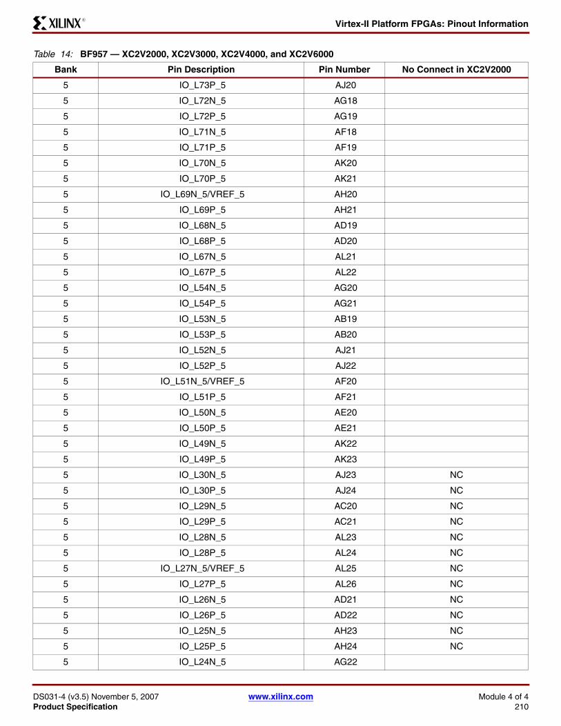
Virtex-II Platform FPGAs: Pinout InformationR
DS031-4 (v3.5) November 5, 2007 www.xilinx.com Module 4 of 4Product Specification 210
5 IO_L73P_5 AJ20
5 IO_L72N_5 AG18
5 IO_L72P_5 AG19
5 IO_L71N_5 AF18
5 IO_L71P_5 AF19
5 IO_L70N_5 AK20
5 IO_L70P_5 AK21
5 IO_L69N_5/VREF_5 AH20
5 IO_L69P_5 AH21
5 IO_L68N_5 AD19
5 IO_L68P_5 AD20
5 IO_L67N_5 AL21
5 IO_L67P_5 AL22
5 IO_L54N_5 AG20
5 IO_L54P_5 AG21
5 IO_L53N_5 AB19
5 IO_L53P_5 AB20
5 IO_L52N_5 AJ21
5 IO_L52P_5 AJ22
5 IO_L51N_5/VREF_5 AF20
5 IO_L51P_5 AF21
5 IO_L50N_5 AE20
5 IO_L50P_5 AE21
5 IO_L49N_5 AK22
5 IO_L49P_5 AK23
5 IO_L30N_5 AJ23 NC
5 IO_L30P_5 AJ24 NC
5 IO_L29N_5 AC20 NC
5 IO_L29P_5 AC21 NC
5 IO_L28N_5 AL23 NC
5 IO_L28P_5 AL24 NC
5 IO_L27N_5/VREF_5 AL25 NC
5 IO_L27P_5 AL26 NC
5 IO_L26N_5 AD21 NC
5 IO_L26P_5 AD22 NC
5 IO_L25N_5 AH23 NC
5 IO_L25P_5 AH24 NC
5 IO_L24N_5 AG22
Table 14: BF957 — XC2V2000, XC2V3000, XC2V4000, and XC2V6000
Bank Pin Description Pin Number No Connect in XC2V2000

Virtex-II Platform FPGAs: Pinout InformationR
DS031-4 (v3.5) November 5, 2007 www.xilinx.com Module 4 of 4Product Specification 211
5 IO_L24P_5 AG23
5 IO_L23N_5 AE22
5 IO_L23P_5 AE23
5 IO_L22N_5 AK25
5 IO_L22P_5 AK26
5 IO_L21N_5/VREF_5 AH25
5 IO_L21P_5 AG25
5 IO_L20N_5 AB21
5 IO_L20P_5 AC22
5 IO_L19N_5 AL27
5 IO_L19P_5 AL28
5 IO_L06N_5 AK27
5 IO_L06P_5 AJ27
5 IO_L05N_5/VRP_5 AD23
5 IO_L05P_5/VRN_5 AE24
5 IO_L04N_5 AJ26
5 IO_L04P_5/VREF_5 AH26
5 IO_L03N_5/D4/ALT_VRP_5 AF23
5 IO_L03P_5/D5/ALT_VRN_5 AF24
5 IO_L02N_5/D6 AG24
5 IO_L02P_5/D7 AF25
5 IO_L01N_5/RDWR_B AK28
5 IO_L01P_5/CS_B AK29
6 IO_L01P_6 AF27
6 IO_L01N_6 AF28
6 IO_L02P_6/VRN_6 AE26
6 IO_L02N_6/VRP_6 AE27
6 IO_L03P_6 AH29
6 IO_L03N_6/VREF_6 AH30
6 IO_L04P_6 AB22
6 IO_L04N_6 AB23
6 IO_L05P_6 AG28
6 IO_L05N_6 AG29
6 IO_L06P_6 AH31
6 IO_L06N_6 AG31
6 IO_L19P_6 AA22
6 IO_L19N_6 Y22
Table 14: BF957 — XC2V2000, XC2V3000, XC2V4000, and XC2V6000
Bank Pin Description Pin Number No Connect in XC2V2000

Virtex-II Platform FPGAs: Pinout InformationR
DS031-4 (v3.5) November 5, 2007 www.xilinx.com Module 4 of 4Product Specification 212
6 IO_L20P_6 AD25
6 IO_L20N_6 AC24
6 IO_L21P_6 AG30
6 IO_L21N_6/VREF_6 AF30
6 IO_L22P_6 AD26
6 IO_L22N_6 AC26
6 IO_L23P_6 AF29
6 IO_L23N_6 AD29
6 IO_L24P_6 AE28
6 IO_L24N_6 AD28
6 IO_L25P_6 AB24 NC
6 IO_L25N_6 AA24 NC
6 IO_L27P_6 AC25 NC
6 IO_L27N_6/VREF_6 AB25 NC
6 IO_L43P_6 AF31
6 IO_L43N_6 AE31
6 IO_L44P_6 AA23
6 IO_L44N_6 Y23
6 IO_L45P_6 AE30
6 IO_L45N_6/VREF_6 AC30
6 IO_L46P_6 AC28
6 IO_L46N_6 AA28
6 IO_L47P_6 AD27
6 IO_L47N_6 AC27
6 IO_L48P_6 AA25
6 IO_L48N_6 Y25
6 IO_L49P_6 AC29
6 IO_L49N_6 AB29
6 IO_L50P_6 AB27
6 IO_L50N_6 AA27
6 IO_L51P_6 AA26
6 IO_L51N_6/VREF_6 Y26
6 IO_L52P_6 AD31
6 IO_L52N_6 AC31
6 IO_L53P_6 W22
6 IO_L53N_6 V22
6 IO_L54P_6 Y27
6 IO_L54N_6 W27
Table 14: BF957 — XC2V2000, XC2V3000, XC2V4000, and XC2V6000
Bank Pin Description Pin Number No Connect in XC2V2000

Virtex-II Platform FPGAs: Pinout InformationR
DS031-4 (v3.5) November 5, 2007 www.xilinx.com Module 4 of 4Product Specification 213
6 IO_L67P_6 AB30
6 IO_L67N_6 AA30
6 IO_L68P_6 W26
6 IO_L68N_6 V26
6 IO_L69P_6 AB31
6 IO_L69N_6/VREF_6 AA31
6 IO_L70P_6 AA29
6 IO_L70N_6 Y29
6 IO_L71P_6 Y24
6 IO_L71N_6 W24
6 IO_L72P_6 V25
6 IO_L72N_6 U25
6 IO_L73P_6 Y28
6 IO_L73N_6 W28
6 IO_L74P_6 W23
6 IO_L74N_6 V23
6 IO_L75P_6 Y30
6 IO_L75N_6/VREF_6 W30
6 IO_L76P_6 Y31
6 IO_L76N_6 W31
6 IO_L77P_6 V27
6 IO_L77N_6 U27
6 IO_L78P_6 W29
6 IO_L78N_6 U29
6 IO_L91P_6 U23
6 IO_L91N_6 T23
6 IO_L92P_6 U26
6 IO_L92N_6 T26
6 IO_L93P_6 V28
6 IO_L93N_6/VREF_6 U28
6 IO_L94P_6 U24
6 IO_L94N_6 T24
6 IO_L95P_6 V30
6 IO_L95N_6 U30
6 IO_L96P_6 V31
6 IO_L96N_6 U31
7 IO_L96P_7 T27
Table 14: BF957 — XC2V2000, XC2V3000, XC2V4000, and XC2V6000
Bank Pin Description Pin Number No Connect in XC2V2000

Virtex-II Platform FPGAs: Pinout InformationR
DS031-4 (v3.5) November 5, 2007 www.xilinx.com Module 4 of 4Product Specification 214
7 IO_L96N_7 R27
7 IO_L95P_7 R24
7 IO_L95N_7 N24
7 IO_L94P_7 T29
7 IO_L94N_7 R29
7 IO_L93P_7/VREF_7 R31
7 IO_L93N_7 P31
7 IO_L92P_7 R26
7 IO_L92N_7 P26
7 IO_L91P_7 R30
7 IO_L91N_7 P30
7 IO_L78P_7 R25
7 IO_L78N_7 P25
7 IO_L77P_7 R28
7 IO_L77N_7 P28
7 IO_L76P_7 N31
7 IO_L76N_7 M31
7 IO_L75P_7/VREF_7 R23
7 IO_L75N_7 P23
7 IO_L74P_7 N30
7 IO_L74N_7 M30
7 IO_L73P_7 P27
7 IO_L73N_7 N27
7 IO_L72P_7 P22
7 IO_L72N_7 N22
7 IO_L71P_7 N29
7 IO_L71N_7 M29
7 IO_L70P_7 N28
7 IO_L70N_7 M28
7 IO_L69P_7/VREF_7 N26
7 IO_L69N_7 M26
7 IO_L68P_7 L31
7 IO_L68N_7 K31
7 IO_L67P_7 M27
7 IO_L67N_7 L27
7 IO_L54P_7 N23
7 IO_L54N_7 M23
7 IO_L53P_7 L30
Table 14: BF957 — XC2V2000, XC2V3000, XC2V4000, and XC2V6000
Bank Pin Description Pin Number No Connect in XC2V2000

Virtex-II Platform FPGAs: Pinout InformationR
DS031-4 (v3.5) November 5, 2007 www.xilinx.com Module 4 of 4Product Specification 215
7 IO_L53N_7 K30
7 IO_L52P_7 L28
7 IO_L52N_7 J28
7 IO_L51P_7/VREF_7 M24
7 IO_L51N_7 L24
7 IO_L50P_7 L29
7 IO_L50N_7 K29
7 IO_L49P_7 M25
7 IO_L49N_7 L25
7 IO_L48P_7 L26
7 IO_L48N_7 J26
7 IO_L47P_7 J31
7 IO_L47N_7 H31
7 IO_L46P_7 J29
7 IO_L46N_7 H29
7 IO_L45P_7/VREF_7 M22
7 IO_L45N_7 L22
7 IO_L44P_7 J30
7 IO_L44N_7 G30
7 IO_L43P_7 K27
7 IO_L43N_7 J27
7 IO_L27P_7/VREF_7 L23 NC
7 IO_L27N_7 K23 NC
7 IO_L25P_7 G31 NC
7 IO_L25N_7 F31 NC
7 IO_L24P_7 F30
7 IO_L24N_7 E30
7 IO_L23P_7 K25
7 IO_L23N_7 J25
7 IO_L22P_7 H28
7 IO_L22N_7 G28
7 IO_L21P_7/VREF_7 H27
7 IO_L21N_7 G27
7 IO_L20P_7 K24
7 IO_L20N_7 J24
7 IO_L19P_7 E31
7 IO_L19N_7 D31
7 IO_L06P_7 F28
Table 14: BF957 — XC2V2000, XC2V3000, XC2V4000, and XC2V6000
Bank Pin Description Pin Number No Connect in XC2V2000

Virtex-II Platform FPGAs: Pinout InformationR
DS031-4 (v3.5) November 5, 2007 www.xilinx.com Module 4 of 4Product Specification 216
7 IO_L06N_7 E28
7 IO_L05P_7 K22
7 IO_L05N_7 K21
7 IO_L04P_7 F29
7 IO_L04N_7 E29
7 IO_L03P_7/VREF_7 H26
7 IO_L03N_7 H25
7 IO_L02P_7/VRN_7 G26
7 IO_L02N_7/VRP_7 F27
7 IO_L01P_7 D30
7 IO_L01N_7 D29
0 VCCO_0 C18
0 VCCO_0 C25
0 VCCO_0 F22
0 VCCO_0 H18
0 VCCO_0 L17
0 VCCO_0 L18
0 VCCO_0 L19
0 VCCO_0 L20
0 VCCO_0 M17
0 VCCO_0 M18
0 VCCO_0 M19
1 VCCO_1 C7
1 VCCO_1 C14
1 VCCO_1 F10
1 VCCO_1 H14
1 VCCO_1 L12
1 VCCO_1 L13
1 VCCO_1 L14
1 VCCO_1 L15
1 VCCO_1 M13
1 VCCO_1 M14
1 VCCO_1 M15
2 VCCO_2 G3
2 VCCO_2 K6
2 VCCO_2 M11
2 VCCO_2 N11
Table 14: BF957 — XC2V2000, XC2V3000, XC2V4000, and XC2V6000
Bank Pin Description Pin Number No Connect in XC2V2000

Virtex-II Platform FPGAs: Pinout InformationR
DS031-4 (v3.5) November 5, 2007 www.xilinx.com Module 4 of 4Product Specification 217
2 VCCO_2 N12
2 VCCO_2 P3
2 VCCO_2 P8
2 VCCO_2 P11
2 VCCO_2 P12
2 VCCO_2 R11
2 VCCO_2 R12
3 VCCO_3 U11
3 VCCO_3 U12
3 VCCO_3 V3
3 VCCO_3 V8
3 VCCO_3 V11
3 VCCO_3 V12
3 VCCO_3 W11
3 VCCO_3 W12
3 VCCO_3 Y11
3 VCCO_3 AB6
3 VCCO_3 AE3
4 VCCO_4 Y13
4 VCCO_4 Y14
4 VCCO_4 Y15
4 VCCO_4 AA12
4 VCCO_4 AA13
4 VCCO_4 AA14
4 VCCO_4 AA15
4 VCCO_4 AD14
4 VCCO_4 AF10
4 VCCO_4 AJ7
4 VCCO_4 AJ14
5 VCCO_5 Y17
5 VCCO_5 Y18
5 VCCO_5 Y19
5 VCCO_5 AA17
5 VCCO_5 AA18
5 VCCO_5 AA19
5 VCCO_5 AA20
5 VCCO_5 AD18
5 VCCO_5 AF22
Table 14: BF957 — XC2V2000, XC2V3000, XC2V4000, and XC2V6000
Bank Pin Description Pin Number No Connect in XC2V2000

Virtex-II Platform FPGAs: Pinout InformationR
DS031-4 (v3.5) November 5, 2007 www.xilinx.com Module 4 of 4Product Specification 218
5 VCCO_5 AJ18
5 VCCO_5 AJ25
6 VCCO_6 U20
6 VCCO_6 U21
6 VCCO_6 V20
6 VCCO_6 V21
6 VCCO_6 V24
6 VCCO_6 V29
6 VCCO_6 W20
6 VCCO_6 W21
6 VCCO_6 Y21
6 VCCO_6 AB26
6 VCCO_6 AE29
7 VCCO_7 G29
7 VCCO_7 K26
7 VCCO_7 M21
7 VCCO_7 N20
7 VCCO_7 N21
7 VCCO_7 P20
7 VCCO_7 P21
7 VCCO_7 P24
7 VCCO_7 P29
7 VCCO_7 R20
7 VCCO_7 R21
NA CCLK AJ4
NA PROG_B D27
NA DONE AG6
NA M0 AH27
NA M1 AJ28
NA M2 AG26
NA HSWAP_EN E26
NA TCK K11
NA TDI C28
NA TDO C4
NA TMS J10
NA PWRDWN_B AH5
NA DXN F25
Table 14: BF957 — XC2V2000, XC2V3000, XC2V4000, and XC2V6000
Bank Pin Description Pin Number No Connect in XC2V2000

Virtex-II Platform FPGAs: Pinout InformationR
DS031-4 (v3.5) November 5, 2007 www.xilinx.com Module 4 of 4Product Specification 219
NA DXP B28
NA VBATT D5
NA RSVD B4
NA VCCAUX B16
NA VCCAUX C2
NA VCCAUX C30
NA VCCAUX T2
NA VCCAUX T30
NA VCCAUX AJ2
NA VCCAUX AJ30
NA VCCAUX AK16
NA VCCINT K15
NA VCCINT K17
NA VCCINT L11
NA VCCINT L16
NA VCCINT L21
NA VCCINT M12
NA VCCINT M16
NA VCCINT M20
NA VCCINT N13
NA VCCINT N14
NA VCCINT N15
NA VCCINT N16
NA VCCINT N17
NA VCCINT N18
NA VCCINT N19
NA VCCINT P13
NA VCCINT P19
NA VCCINT R10
NA VCCINT R13
NA VCCINT R19
NA VCCINT R22
NA VCCINT T11
NA VCCINT T12
NA VCCINT T13
NA VCCINT T19
NA VCCINT T20
Table 14: BF957 — XC2V2000, XC2V3000, XC2V4000, and XC2V6000
Bank Pin Description Pin Number No Connect in XC2V2000

Virtex-II Platform FPGAs: Pinout InformationR
DS031-4 (v3.5) November 5, 2007 www.xilinx.com Module 4 of 4Product Specification 220
NA VCCINT T21
NA VCCINT U10
NA VCCINT U13
NA VCCINT U19
NA VCCINT U22
NA VCCINT V13
NA VCCINT V19
NA VCCINT W13
NA VCCINT W14
NA VCCINT W15
NA VCCINT W16
NA VCCINT W17
NA VCCINT W18
NA VCCINT W19
NA VCCINT Y12
NA VCCINT Y16
NA VCCINT Y20
NA VCCINT AA11
NA VCCINT AA16
NA VCCINT AA21
NA VCCINT AB15
NA VCCINT AB17
NA GND A2
NA GND A3
NA GND A16
NA GND A29
NA GND A30
NA GND B1
NA GND B2
NA GND B8
NA GND B24
NA GND B30
NA GND B31
NA GND C1
NA GND C3
NA GND C29
NA GND C31
NA GND D4
Table 14: BF957 — XC2V2000, XC2V3000, XC2V4000, and XC2V6000
Bank Pin Description Pin Number No Connect in XC2V2000

Virtex-II Platform FPGAs: Pinout InformationR
DS031-4 (v3.5) November 5, 2007 www.xilinx.com Module 4 of 4Product Specification 221
NA GND D10
NA GND D16
NA GND D22
NA GND D28
NA GND E5
NA GND E27
NA GND F6
NA GND F26
NA GND G7
NA GND G13
NA GND G16
NA GND G19
NA GND G25
NA GND H2
NA GND H8
NA GND H24
NA GND H30
NA GND J9
NA GND J23
NA GND K4
NA GND K16
NA GND K28
NA GND N7
NA GND N25
NA GND P14
NA GND P15
NA GND P16
NA GND P17
NA GND P18
NA GND R14
NA GND R15
NA GND R16
NA GND R17
NA GND R18
NA GND T1
NA GND T4
NA GND T7
NA GND T10
Table 14: BF957 — XC2V2000, XC2V3000, XC2V4000, and XC2V6000
Bank Pin Description Pin Number No Connect in XC2V2000

Virtex-II Platform FPGAs: Pinout InformationR
DS031-4 (v3.5) November 5, 2007 www.xilinx.com Module 4 of 4Product Specification 222
NA GND T14
NA GND T15
NA GND T16
NA GND T17
NA GND T18
NA GND T22
NA GND T25
NA GND T28
NA GND T31
NA GND U14
NA GND U15
NA GND U16
NA GND U17
NA GND U18
NA GND V14
NA GND V15
NA GND V16
NA GND V17
NA GND V18
NA GND W7
NA GND W25
NA GND AB4
NA GND AB16
NA GND AB28
NA GND AC9
NA GND AC23
NA GND AD2
NA GND AD8
NA GND AD24
NA GND AD30
NA GND AE7
NA GND AE13
NA GND AE16
NA GND AE19
NA GND AE25
NA GND AF6
NA GND AF26
NA GND AG5
Table 14: BF957 — XC2V2000, XC2V3000, XC2V4000, and XC2V6000
Bank Pin Description Pin Number No Connect in XC2V2000

Virtex-II Platform FPGAs: Pinout InformationR
DS031-4 (v3.5) November 5, 2007 www.xilinx.com Module 4 of 4Product Specification 223
NA GND AG27
NA GND AH4
NA GND AH10
NA GND AH16
NA GND AH22
NA GND AH28
NA GND AJ1
NA GND AJ3
NA GND AJ29
NA GND AJ31
NA GND AK1
NA GND AK2
NA GND AK8
NA GND AK24
NA GND AK30
NA GND AK31
NA GND AL2
NA GND AL3
NA GND AL16
NA GND AL29
NA GND AL30
Notes: 1. See Table 4 for an explanation of the signals available on this pin.
Table 14: BF957 — XC2V2000, XC2V3000, XC2V4000, and XC2V6000
Bank Pin Description Pin Number No Connect in XC2V2000

Virtex-II Platform FPGAs: Pinout InformationR
DS031-4 (v3.5) November 5, 2007 www.xilinx.com Module 4 of 4Product Specification 224
BF957 Flip-Chip BGA Package Specifications (1.27mm pitch)
Figure 10: BF957 Flip-Chip BGA Package Specifications

Virtex-II Platform FPGAs: Pinout InformationR
DS031-4 (v3.5) November 5, 2007 www.xilinx.com Module 4 of 4Product Specification 225
Revision HistoryThis section records the change history for this module of the data sheet.
Date Version Revision
11/07/00 1.0 Early access draft.
11/22/00 1.1 Initial Xilinx release. Made the following corrections:CS144 package - Table 5, page 5:• Added missing pin D10 in Bank 1.• Changed dedicated pins A2 and B2 to RSVD (from DXN and DXP).FG256 package - Table 6, page 10:• Changed dedicated pins A3 and A4 to RSVD (from DXN and DXP).FG896 package - Table 11, page 94:• Corrected pin AG1 in Bank 4 to be AG12.FF1152 package - Table 12, page 120:• Corrected pin Y3 in Bank 6 to be Y32.
12/19/00 1.2 Reverse designations were fixed for pins in every package.
01/25/01 1.3 Data sheet divided into four modules (per current style standard). DXN and DXP pin information added for CS144 package (Table 5) and FG256 package (Table 6).
02/07/01 1.4 DXN and DXP pin information was changed back to RSVD for the CS144 package (Table 5) and the FG256 package (Table 6).
04/02/01 1.5 • ALT_VRN and ALT_VRP pin information was added for each package. • Table 8, page 34 – added No Connect designations for the XC2V1500 device in the
FG676 package.• Reverted to traditional double-column format.
11/07/01 1.6 • Updated list of devices supported in the FF1152, FF1517, and BF957 packages.
09/26/02 1.7 • Updated Table 3 to reflect devices supported in the BG728 and BF957 packages.• Added mention of LVPECL to pin definition in Table 4.
10/07/02 1.8 • Corrected Table 10 heading to reflect supported devices in the BG728 package.
12/06/02 1.8.1 • Enhanced the description of the PWRDWN_B pin in Table 4.
05/07/03 1.8.2 • Added clarification to Table 4 and all device pinout tables regarding the dual-use nature of pins D0/DIN and BUSY/DOUT during configuration.
06/19/03 1.8.3 • The final GND pin in each of five pinout tables was inadvertently deleted in v1.8.2. This revision restores the deleted GND pins as follows:- Pin C5, Table 5, page 5 (CS144)- Pin A1, Table 6, page 10 (FG256)- Pin A2, Table 10, page 72 (BG728)- Pin A2, Table 12, page 120 (FF1152)- Pin AL30, Table 14, page 198 (BF957)
08/01/03 2.0 All Virtex-II devices and speed grades now Production. See Table 13, Module 3.
03/29/04 2.0.1 Recompiled for backward compatibility with Acrobat 4 and above.
06/24/04 3.3 Added references to, and new package drawings for, Pb-free wire-bond packages CSG, FGG, and BGG. (Revision number advanced to level of complete data sheet.)
03/01/05 3.4 Table 4: Changed Direction for User I/O pins (IO_LXXY_#) from “Input/Output” to “Input/Output/Bidirectional”. Added requirement to VBATT to connect pin to VCCAUX or GND if battery is not used.
11/05/07 3.5 Updated copyright notice and legal disclaimer.

Virtex-II Platform FPGAs: Pinout InformationR
DS031-4 (v3.5) November 5, 2007 www.xilinx.com Module 4 of 4Product Specification 226
Notice of DisclaimerTHE XILINX HARDWARE FPGA AND CPLD DEVICES REFERRED TO HEREIN (“PRODUCTS”) ARE SUBJECT TO THE TERMS ANDCONDITIONS OF THE XILINX LIMITED WARRANTY WHICH CAN BE VIEWED AT http://www.xilinx.com/warranty.htm. THIS LIMITEDWARRANTY DOES NOT EXTEND TO ANY USE OF PRODUCTS IN AN APPLICATION OR ENVIRONMENT THAT IS NOT WITHIN THESPECIFICATIONS STATED IN THE XILINX DATA SHEET. ALL SPECIFICATIONS ARE SUBJECT TO CHANGE WITHOUT NOTICE.PRODUCTS ARE NOT DESIGNED OR INTENDED TO BE FAIL-SAFE OR FOR USE IN ANY APPLICATION REQUIRING FAIL-SAFEPERFORMANCE, SUCH AS LIFE-SUPPORT OR SAFETY DEVICES OR SYSTEMS, OR ANY OTHER APPLICATION THAT INVOKESTHE POTENTIAL RISKS OF DEATH, PERSONAL INJURY, OR PROPERTY OR ENVIRONMENTAL DAMAGE (“CRITICALAPPLICATIONS”). USE OF PRODUCTS IN CRITICAL APPLICATIONS IS AT THE SOLE RISK OF CUSTOMER, SUBJECT TOAPPLICABLE LAWS AND REGULATIONS.
Virtex-II Data SheetThe Virtex-II Data Sheet contains the following modules:
• Virtex-II Platform FPGAs: Introduction and Overview (Module 1)
• Virtex-II Platform FPGAs: Functional Description (Module 2)
• Virtex-II Platform FPGAs: DC and Switching Characteristics (Module 3)
• Virtex-II Platform FPGAs: Pinout Information (Module 4)