xc18v00 series in-system-programmable configuration proms
TRANSCRIPT
DS026 (v6.1) February 5, 2019 www.xilinx.comProduct Specification 1
© 1999–2019 Xilinx, Inc. Xilinx, the Xilinx logo, Alveo, Artix, ISE, Kintex, Spartan, Versal, Virtex, Vivado, Zynq, and other designated brands included herein are trademarks of Xilinx in the United States and other countries.
Features• In-System Programmable 3.3V PROMs for
Configuration of Xilinx FPGAs
♦ Endurance of 20,000 Program/Erase Cycles
♦ Program/Erase Over Full Industrial Voltage and Temperature Range (–40°C to +85°C)
• IEEE Std 1149.1 Boundary-Scan (JTAG) Support
• JTAG Command Initiation of Standard FPGA Configuration
• Simple Interface to the FPGA
• Cascadable for Storing Longer or Multiple Bitstreams
• Low-Power Advanced CMOS FLASH Process
• Dual Configuration Modes
♦ Serial Slow/Fast Configuration (up to 33 MHz)
♦ Parallel (up to 264 Mb/s at 33 MHz)
• 5V-Tolerant I/O Pins Accept 5V, 3.3V and 2.5V Signals
• 3.3V or 2.5V Output Capability
• Design Support Using the Xilinx ISE™ Foundation™ Software Packages
• Available in PC20, SO20, PC44, and VQ44 Packages
• Lead-Free (Pb-Free) Packaging
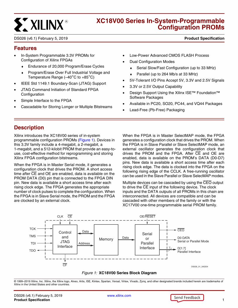
DescriptionXilinx introduces the XC18V00 series of in-system programmable configuration PROMs (Figure 1). Devices in this 3.3V family include a 4-megabit, a 2-megabit, a 1-megabit, and a 512-kilobit PROM that provide an easy-to-use, cost-effective method for reprogramming and storing Xilinx FPGA configuration bitstreams.
When the FPGA is in Master Serial mode, it generates a configuration clock that drives the PROM. A short access time after CE and OE are enabled, data is available on the PROM DATA (D0) pin that is connected to the FPGA DIN pin. New data is available a short access time after each rising clock edge. The FPGA generates the appropriate number of clock pulses to complete the configuration. When the FPGA is in Slave Serial mode, the PROM and the FPGA are clocked by an external clock.
When the FPGA is in Master SelectMAP mode, the FPGAgenerates a configuration clock that drives the PROM. Whenthe FPGA is in Slave Parallel or Slave SelectMAP mode, anexternal oscillator generates the configuration clock thatdrives the PROM and the FPGA. After CE and OE areenabled, data is available on the PROM’s DATA (D0-D7)pins. New data is available a short access time after eachrising clock edge. The data is clocked into the FPGA on thefollowing rising edge of the CCLK. A free-running oscillatorcan be used in the Slave Parallel or Slave SelecMAP modes.
Multiple devices can be cascaded by using the CEO output to drive the CE input of the following device. The clock inputs and the DATA outputs of all PROMs in this chain are interconnected. All devices are compatible and can be cascaded with other members of the family or with the XC17V00 one-time programmable serial PROM family.
25XC18V00 Series In-System-Programmable
Configuration PROMs
DS026 (v6.1) February 5, 2019 0 Product Specification
R
X-Ref Target - Figure 1
Figure 1: XC18V00 Series Block Diagram
Controland
JTAGInterface
MemorySerial
orParallel
Interface
D0 DATASerial or Parallel Mode
D[1:7]Parallel Interface
Data
Address
CLK CE
TCK
TMS
TDI
TDO
OE/RESET
CEO
Data
DS026_01_040204
7
CF
Send Feedback

XC18V00 Series In-System-Programmable Configuration PROMs
DS026 (v6.1) February 5, 2019 www.xilinx.comProduct Specification 2
R
Pinout and Pin DescriptionTable 1 provides a list of the pin names and descriptions for the 44-pin VQFP and PLCC and the 20-pin SOIC and PLCCpackages.
Table 1: Pin Names and Descriptions
Pin Name
Boundary- Scan Order Function Pin Description 44-pin VQFP 44-pin
PLCC
20-pinSOIC &PLCC
D0 4 DATA OUT D0 is the DATA output pin to provide data for configuring an FPGA in serial mode.
40 2 1
3 OUTPUT ENABLE
D1 6 DATA OUT D0-D7 are the output pins to provide parallel data for configuring a Xilinx FPGA in Slave Parallel/SelectMAP mode.
D1-D7 remain in high-Z state when the PROM operates in serial mode.
D1-D7 can be left unconnected when the PROM is used in serial mode.
29 35 16
5 OUTPUT ENABLE
D2 2 DATA OUT 42 4 2
1 OUTPUT ENABLE
D3 8 DATA OUT 27 33 15
7 OUTPUT ENABLE
D4 24 DATA OUT 9 15 7(1)
23 OUTPUT ENABLE
D5 10 DATA OUT 25 31 14
9 OUTPUT ENABLE
D6 17 DATA OUT 14 20 9
16 OUTPUT ENABLE
D7 14 DATA OUT 19 25 12
13 OUTPUT ENABLE
CLK 0 DATA IN Each rising edge on the CLK input increments the internal address counter if both CE is Low and OE/RESET is High.
43 5 3
OE/RESET
20 DATA IN When Low, this input holds the address counter reset and the DATA output is in a high-Z state. This is a bidirectional open-drain pin that is held Low while the PROM is reset. Polarity is NOT programmable.
13 19 8
19 DATA OUT
18 OUTPUT ENABLE
CE 15 DATA IN When CE is High, the device is put into low-power standby mode, the address counter is reset, and the DATA pins are put in a high-Z state.
15 21 10
CF 22 DATA OUT Allows JTAG CONFIG instruction to initiate FPGA configuration without powering down FPGA. This is an open-drain output that is pulsed Low by the JTAG CONFIG command.
10 16 7(1)
21 OUTPUT ENABLE
Send Feedback

XC18V00 Series In-System-Programmable Configuration PROMs
DS026 (v6.1) February 5, 2019 www.xilinx.comProduct Specification 3
R
CEO 12 DATA OUT Chip Enable Output (CEO) is connected to the CE input of the next PROM in the chain. This output is Low when CE is Low and OE/RESET input is High, AND the internal address counter has been incremented beyond its Terminal Count (TC) value. CEO returns to High when OE/RESET goes Low or CE goes High.
21 27 13
11 OUTPUT ENABLE
GND GND is the ground connection. 6, 18, 28 & 41 3, 12, 24 & 34
11
TMS MODE SELECT
The state of TMS on the rising edge of TCK determines the state transitions at the Test Access Port (TAP) controller. TMS has an internal 50 kΩ resistive pull-up to provide a logic 1 to the device if the pin is not driven.
5 11 5
TCK CLOCK This pin is the JTAG test clock. It sequences the TAP controller and all the JTAG test and programming electronics.
7 13 6
TDI DATA IN This pin is the serial input to all JTAG instruction and data registers. TDI has an internal 50 kΩ resistive pull-up to provide a logic 1 to the device if the pin is not driven.
3 9 4
TDO DATA OUT This pin is the serial output for all JTAG instruction and data registers. TDO has an internal 50 kΩ resistive pull-up to provide a logic 1 to the system if the pin is not driven.
31 37 17
VCCINT Positive 3.3V supply voltage for internal logic. 17, 35 & 38(3) 23, 41 & 44(3)
18 & 20(3)
VCCO Positive 3.3V or 2.5V supply voltage connected to the input buffers(2) and output voltage drivers.
8, 16, 26 & 36 14, 22, 32 & 42
19
NC No connects. 1, 2, 4,11, 12, 20, 22, 23, 24, 30, 32, 33, 34, 37, 39,
44
1, 6, 7, 8, 10, 17, 18, 26, 28, 29, 30, 36, 38, 39, 40, 43
Notes: 1. By default, pin 7 is the D4 pin in the 20-pin packages. However, CF → D4 programming option can be set to override the default and route
the CF function to pin 7 in the Serial mode.2. For devices with IDCODES 0502x093h, the input buffers are supplied by VCCINT.3. For devices with IDCODES 0503x093h, the following VCCINT pins are no-connects: pin 38 in 44-pin VQFP package, pin 44 in 44-pin PLCC
package, and pin 20 in 20-pin SOIC and 20-pin PLCC packages.
Table 1: Pin Names and Descriptions (Cont’d)
Pin Name
Boundary- Scan Order Function Pin Description 44-pin VQFP 44-pin
PLCC
20-pinSOIC &PLCC
Send Feedback

XC18V00 Series In-System-Programmable Configuration PROMs
DS026 (v6.1) February 5, 2019 www.xilinx.comProduct Specification 4
R
Pinout Diagrams
6 5 4 3 2 1 44 43 42 41 40
3938373635343332313029
18 19 20 21 22 23 24 25 26 27 28
7891011121314151617
PC44/PCG44Top View
NCNCTDONCD1GNDD3VCCOD5NCNC
NC
OE
/RE
SE
TD
6C
EV
CC
OV
CC
INT
*G
ND D7
NC
CE
ON
C
NCNCTDINC
TMSGNDTCK
VCCOD4CFNC
NC
CLK
D2
GN
DD
0N
CV
CC
INT
*N
CV
CC
OV
CC
INT
*N
C
DS026_12_20051007
*See pin descriptions.
1234567891011
VQ44/VQG44Top View
NCNCTDONCD1GNDD3VCCOD5NCNC
NC
OE
/RE
SE
TD
6C
EV
CC
OV
CC
INT
*G
ND D7
NC
CE
ON
C
NCNCTDINC
TMSGNDTCK
VCCOD4CFNC
NC
CLK
D2
GN
DD
0N
CV
CC
INT
*N
CV
CC
OV
CC
INT
*N
C
DS026_13_20051007
44 43 42 41 40 39 38 37 36 35 34
3332313029282726252423
12 13 14 15 16 17 18 19 20 21 22
*See pin descriptions.
SO20/SOG20
Top View
DS026_14_102005
*See pin descriptions.
1
2
3
4
5
6
7
8
9
10
DATA(D0)
D2
CLK
TDI
TMS
TCK
CF/D4*
OE/RESET
D6
CE
20
19
18
17
16
15
14
13
12
11
VCCINT*
VCCO
VCCINT*
TDO
D1
D3
D5
CEO
D7
GND
SO20/SOG20
Top View
DS026_14_102005
*See pin descriptions.
1
2
3
4
5
6
7
8
9
10
DATA(D0)
D2
CLK
TDI
TMS
TCK
CF/D4*
OE/RESET
D6
CE
20
19
18
17
16
15
14
13
12
11
VCCINT*
VCCO
VCCINT*
TDO
D1
D3
D5
CEO
D7
GND
PC20/PCG20
Top View
DS026_15_200510073 2 1 20 19
18
17
16
15
14
9 10 11 12 13
4
5
6
7
8
CLK
D2
D0
VC
CIN
T*
VC
CO
VCCINT*
TDO
D1
D3
D5
D6
CE
GN
D D7
CE
O
TDI
TMS
TCK
D4/CF*
OE/RESET
*See pin descriptions.
Send Feedback

XC18V00 Series In-System-Programmable Configuration PROMs
DS026 (v6.1) February 5, 2019 www.xilinx.comProduct Specification 5
R
Xilinx FPGAs and Compatible PROMsTable 2 provides a list of Xilinx FPGAs and compatible PROMs.
Capacity
Table 2: Xilinx FPGAs and Compatible PROMs
Device Configuration Bits XC18V00 Solution
XC2VP2 1,305,376 XC18V02
XC2VP4 3,006,496 XC18V04
XC2VP7 4,485,408 XC18V04 + XC18V512
XC2VP20 8,214,560 2 of XC18V04
XC2VP30 11,589,920 3 of XC18V04
XC2VP40 15,868,192 4 of XC18V04
XC2VP50 19,021,344 5 of XC18V04
XC2VP70 26,098,976 6 of XC18V04 + XC18V512
XC2VP100 34,292,768 8 of XC18V04 + XC18V512
XC2V40 470,048 XC18V512
XC2V80 732,576 XC18V01
XC2V250 1,726,880 XC18V02
XC2V500 2,767,520 XC18V04
XC2V1000 4,089,504 XC18V04
XC2V1500 5,667,488 XC18V04+ XC18V02
XC2V2000 7,501,472 2 of XC18V04
XC2V3000 10,505,120 3 of XC18V04
XC2V4000 15,673,248 4 of XC18V04
XC2V6000 21,865,376 5 of XC18V04 + XC18V02
XC2V8000 29,081,504 7 of XC18V04
XCV50 559,200 XC18V01
XCV100 781,216 XC18V01
XCV150 1,040,096 XC18V01
XCV200 1,335,840 XC18V02
XCV300 1,751,808 XC18V02
XCV400 2,546,048 XC18V04
XCV600 3,607,968 XC18V04
XCV800 4,715,616 XC18V04 + XC18V512
XCV1000 6,127,744 XC18V04 + XC18V02
XCV50E 630,048 XC18V01
XCV100E 863,840 XC18V01
XCV200E 1,442,016 XC18V02
XCV300E 1,875,648 XC18V02
XCV400E 2,693,440 XC18V04
XCV405E 3,430,400 XC18V04
XCV600E 3,961,632 XC18V04
XCV812E 6,519,648 2 of XC18V04
XCV1000E 6,587,520 2 of XC18V04
XCV1600E 8,308,992 2 of XC18V04
XCV2000E 10,159,648 3 of XC18V04
XCV2600E 12,922,336 4 of XC18V04
XCV3200E 16,283,712 4 of XC18V04
XC2S15 197,696 XC18V512
XC2S30 336,768 XC18V512
XC2S50 559,200 XC18V01
XC2S100 781,216 XC18V01
XC2S150 1,040,096 XC18V01
XC2S200 1,335,840 XC18V02
XC2S50E 630,048 XC18V01
XC2S100E 863,840 XC18V01
XC2S150E 1,134,496 XC18V02
XC2S200E 1,442,016 XC18V02
XC2S300E 1,875,648 XC18V02
XC2S400E 2,693,440 XC18V04
XC2S600E 3,961,632 XC18V04
XC3S50 439,264 XC18V512
XC3S200 1,047,616 XC18V01
XC3S400 1,699,136 XC18V02
XC3S1000 3,223,488 XC18V04
XC3S1500 5,214,784 XC18V04 + XC18V01
XC3S2000 7,673,024 2 of XC18V04
XC3S4000 11,316,864 3 of XC18V04
XC3S5000 13,271,936 3 of XC18V04 + XC18V01
Devices Configuration Bits
XC18V04 4,194,304
XC18V02 2,097,152
XC18V01 1,048,576
XC18V512 524,288
Table 2: Xilinx FPGAs and Compatible PROMs (Cont’d)
Device Configuration Bits XC18V00 Solution
Send Feedback

XC18V00 Series In-System-Programmable Configuration PROMs
DS026 (v6.1) February 5, 2019 www.xilinx.comProduct Specification 6
R
In-System ProgrammingIn-System Programmable PROMs can be programmed individually, or two or more can be chained together and programmed in-system via the standard 4-pin JTAG protocol as shown in Figure 2. In-system programming offers quick and efficient design iterations and eliminates unnecessary package handling or socketing of devices. The Xilinx development system provides the programming data sequence using either Xilinx iMPACT software and a download cable, a third-party JTAG development system, a JTAG-compatible board tester, or a simple microprocessor interface that emulates the JTAG instruction sequence. The iMPACT software also outputs serial vector format (SVF) files for use with any tools that accept SVF format and with automatic test equipment.
All outputs are held in a high-Z state or held at clamp levels during in-system programming.
OE/RESET
The ISP programming algorithm requires issuance of a reset that causes OE to go Low.
External ProgrammingXilinx reprogrammable PROMs can also be programmed by a third-party device programmer, providing the added flexibility of using pre-programmed devices with an in-
system programmable option for future enhancements and design changes.
Reliability and EnduranceXilinx in-system programmable products provide a guaranteed endurance level of 20,000 in-system program/erase cycles and a minimum data retention of 20 years. Each device meets all functional, performance, and data retention specifications within this endurance limit. See the UG116, Xilinx Device Reliability Report, for device quality, reliability, and process node information.
Design SecurityThe Xilinx in-system programmable PROM devices incorporate advanced data security features to fully protect the programming data against unauthorized reading via JTAG. Table 3 shows the security setting available.
The read security bit can be set by the user to prevent the internal programming pattern from being read or copied via JTAG. When set, it allows device erase. Erasing the entire device is the only way to reset the read security bit.
Table 3: Data Security Options
Reset Set
Read AllowedProgram/Erase Allowed
Verify Allowed
Read Inhibited via JTAGProgram/Erase Allowed
Verify Inhibited
X-Ref Target - Figure 2
Figure 2: In-System Programming Operation (a) Solder Device to PCB and (b) Program Using Download Cable
DS026_02_06/1103
GND
V CCINT
(a) (b)
Send Feedback
XC18V00 Series In-System-Programmable Configuration PROMs
DS026 (v6.1) February 5, 2019 www.xilinx.comProduct Specification 7
R
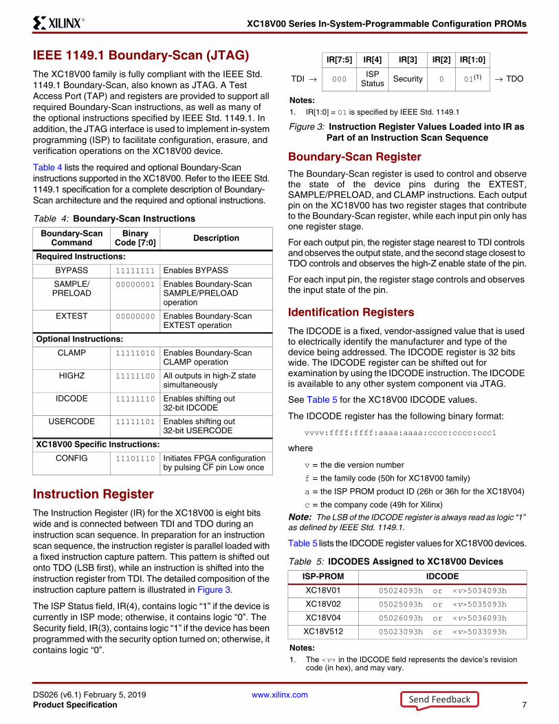
IEEE 1149.1 Boundary-Scan (JTAG)The XC18V00 family is fully compliant with the IEEE Std. 1149.1 Boundary-Scan, also known as JTAG. A Test Access Port (TAP) and registers are provided to support all required Boundary-Scan instructions, as well as many of the optional instructions specified by IEEE Std. 1149.1. In addition, the JTAG interface is used to implement in-system programming (ISP) to facilitate configuration, erasure, and verification operations on the XC18V00 device.
Table 4 lists the required and optional Boundary-Scan instructions supported in the XC18V00. Refer to the IEEE Std. 1149.1 specification for a complete description of Boundary-Scan architecture and the required and optional instructions.
Instruction RegisterThe Instruction Register (IR) for the XC18V00 is eight bits wide and is connected between TDI and TDO during an instruction scan sequence. In preparation for an instruction scan sequence, the instruction register is parallel loaded with a fixed instruction capture pattern. This pattern is shifted out onto TDO (LSB first), while an instruction is shifted into the instruction register from TDI. The detailed composition of the instruction capture pattern is illustrated in Figure 3.
The ISP Status field, IR(4), contains logic “1” if the device is currently in ISP mode; otherwise, it contains logic “0”. The Security field, IR(3), contains logic “1” if the device has been programmed with the security option turned on; otherwise, it contains logic “0”.
X-Ref Target - Figure 3
Boundary-Scan RegisterThe Boundary-Scan register is used to control and observethe state of the device pins during the EXTEST,SAMPLE/PRELOAD, and CLAMP instructions. Each outputpin on the XC18V00 has two register stages that contributeto the Boundary-Scan register, while each input pin only hasone register stage.
For each output pin, the register stage nearest to TDI controls and observes the output state, and the second stage closest to TDO controls and observes the high-Z enable state of the pin.
For each input pin, the register stage controls and observes the input state of the pin.
Identification Registers
The IDCODE is a fixed, vendor-assigned value that is used to electrically identify the manufacturer and type of the device being addressed. The IDCODE register is 32 bits wide. The IDCODE register can be shifted out for examination by using the IDCODE instruction. The IDCODE is available to any other system component via JTAG.
See Table 5 for the XC18V00 IDCODE values.
The IDCODE register has the following binary format:
vvvv:ffff:ffff:aaaa:aaaa:cccc:cccc:ccc1where
v = the die version number
f = the family code (50h for XC18V00 family)
a = the ISP PROM product ID (26h or 36h for the XC18V04)
c = the company code (49h for Xilinx)
Note: The LSB of the IDCODE register is always read as logic “1” as defined by IEEE Std. 1149.1.
Table 5 lists the IDCODE register values for XC18V00 devices.
Table 4: Boundary-Scan Instructions
Boundary-Scan Command
Binary Code [7:0] Description
Required Instructions:
BYPASS 11111111 Enables BYPASS
SAMPLE/PRELOAD
00000001 Enables Boundary-Scan SAMPLE/PRELOAD operation
EXTEST 00000000 Enables Boundary-Scan EXTEST operation
Optional Instructions:
CLAMP 11111010 Enables Boundary-Scan CLAMP operation
HIGHZ 11111100 All outputs in high-Z state simultaneously
IDCODE 11111110 Enables shifting out 32-bit IDCODE
USERCODE 11111101 Enables shifting out 32-bit USERCODE
XC18V00 Specific Instructions:
CONFIG 11101110 Initiates FPGA configuration by pulsing CF pin Low once
IR[7:5] IR[4] IR[3] IR[2] IR[1:0]
TDI → 000 ISPStatus Security 0 01(1) → TDO
Notes: 1. IR[1:0] = 01 is specified by IEEE Std. 1149.1
Figure 3: Instruction Register Values Loaded into IR as Part of an Instruction Scan Sequence
Table 5: IDCODES Assigned to XC18V00 Devices
ISP-PROM IDCODE
XC18V01 05024093h or <v>5034093hXC18V02 05025093h or <v>5035093hXC18V04 05026093h or <v>5036093hXC18V512 05023093h or <v>5033093h
Notes: 1. The <v> in the IDCODE field represents the device’s revision
code (in hex), and may vary.
Send Feedback

XC18V00 Series In-System-Programmable Configuration PROMs
DS026 (v6.1) February 5, 2019 www.xilinx.comProduct Specification 8
R
The USERCODE instruction gives access to a 32-bit user programmable scratch pad typically used to supply information about the device’s programmed contents. By using the USERCODE instruction, a user-programmable identification code can be shifted out for examination. This code is loaded into the USERCODE register during programming of the XC18V00 device. If the device is blank or was not loaded during programming, the USERCODE register contains FFFFFFFFh.
XC18V00 TAP CharacteristicsThe XC18V00 family performs both in-system programming and IEEE 1149.1 Boundary-Scan (JTAG) testing via a single four-wire Test Access Port (TAP). This simplifies system designs and allows standard Automatic Test Equipment to perform both functions. The AC characteristics of the XC18V00 TAP are described as follows.
TAP TimingFigure 4 shows the timing relationships of the TAP signals. These TAP timing characteristics are identical for both Boundary-Scan and ISP operations.
TAP AC ParametersTable 6 shows the timing parameters for the TAP waveforms shown in Figure 4.
X-Ref Target - Figure 4
Figure 4: Test Access Port Timing
Table 6: Test Access Port Timing Parameters
Symbol Parameter Min Max Units
TCKMIN1 TCK minimum clock period 100 – ns
TCKMIN2 TCK minimum clock period, Bypass mode 50 – ns
TMSS TMS setup time 10 – ns
TMSH TMS hold time 25 – ns
TDIS TDI setup time 10 – ns
TDIH TDI hold time 25 – ns
TDOV TDO valid delay – 25 ns
TCK
TCKMIN1,2
TMSS
TMS
TDI
TDO
TMSH
TDIH
TDOV
TDIS
DS026_04_032702
Send Feedback
XC18V00 Series In-System-Programmable Configuration PROMs
DS026 (v6.1) February 5, 2019 www.xilinx.comProduct Specification 9
R
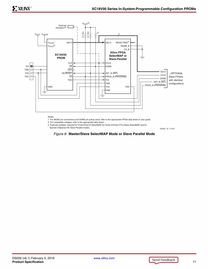
Connecting Configuration PROMs Connecting the FPGA device with the configuration PROM(see Figure 5 and Figure 6).
• The DATA output(s) of the PROM(s) drives the DIN input of the lead FPGA device.
• The Master FPGA CCLK output drives the CLK input(s) of the PROM(s) (in Master Serial and Master SelectMAP modes only).
• The CEO output of a PROM drives the CE input of the next PROM in a daisy chain (if any).
• The OE/RESET pins of all PROMs are connected to the INIT pins of all FPGA devices. This connection assures that the PROM address counter is reset before the start of any (re)configuration, even when a reconfiguration is initiated by a VCCINT glitch.
• The PROM CE input can be driven from the DONE pin. The CE input of the first (or only) PROM can be driven by the DONE output of all target FPGA devices, provided that DONE is not permanently grounded. CE can also be permanently tied Low, but this keeps the DATA output active and causes an unnecessary supply current of 10 mA maximum.
• Slave Parallel/SelectMap mode is similar to slave serial mode. The DATA is clocked out of the PROM one byte per CCLK instead of one bit per CCLK cycle. See FPGA data sheets for special configuration requirements.
Initiating FPGA Configuration
The XC18V00 devices incorporate a pin named CF that is controllable through the JTAG CONFIG instruction. Executing the CONFIG instruction through JTAG pulses the CF Low once for 300–500 ns, which resets the FPGA and initiates configuration.
The CF pin must be connected to the PROGRAM pin on the FPGA(s) to use this feature.
The iMPACT software can also issue a JTAG CONFIG command to initiate FPGA configuration through the “Load FPGA” setting.
The 20-pin packages do not have a dedicated CF pin. For 20-pin packages, the CF → D4 setting can be used to route the CF pin function to pin 7 only if the parallel output mode is not used.
Selecting Configuration Modes
The XC18V00 accommodates serial and parallel methods of configuration. The configuration modes are selectable through a user control register in the XC18V00 device. This control register is accessible through JTAG, and is set using the “Parallel mode” setting on the Xilinx iMPACT software. Serial output is the default configuration mode.
Master Serial Mode SummaryThe I/O and logic functions of the FPGA’s configurable logic block (CLB) and their associated interconnections are established by a configuration program. The program is loaded either automatically upon power up, or on command, depending on the state of the three FPGA mode pins. In Master Serial mode, the FPGA automatically loads the configuration program from an external memory. Xilinx PROMs are designed to accommodate the Master Serial mode.
Upon power-up or reconfiguration, an FPGA enters the Master Serial mode whenever all three of the FPGA mode-select pins are Low (M0=0, M1=0, M2=0). Data is read from the PROM sequentially on a single data line. Synchronization is provided by the rising edge of the temporary signal CCLK, which is generated by the FPGA during configuration.
Master Serial mode provides a simple configuration interface. Only a serial data line, a clock line, and two control lines are required to configure an FPGA. Data from the PROM is read sequentially, accessed via the internal address and bit counters which are incremented on every valid rising edge of CCLK. If the user-programmable, dual-function DIN pin on the FPGA is used only for configuration, it must still be held at a defined level during normal operation. The Xilinx FPGA families take care of this automatically with an on-chip pull-up resistor.
Cascading Configuration PROMs
For multiple FPGAs configured as a serial daisy-chain, or a single FPGA requiring larger configuration memories in a serial or SelectMAP configuration mode, cascaded PROMs provide additional memory (Figure 7 and Figure 8). Multiple XC18V00 devices can be cascaded by using the CEO output to drive the CE input of the downstream device. The clock inputs and the data outputs of all XC18V00 devices in the chain are interconnected. After the last data from the first PROM is read, the next clock signal to the PROM asserts its CEO output Low and drives its DATA line to a high-Z state. The second PROM recognizes the Low level on its CE input and enables its DATA output.
After configuration is complete, address counters of all cascaded PROMs are reset if the PROM OE/RESET pin goes Low or CE goes High.
Send Feedback

XC18V00 Series In-System-Programmable Configuration PROMs
DS026 (v6.1) February 5, 2019 www.xilinx.comProduct Specification 10
R
X-Ref Target - Figure 5
Figure 5: Master Serial Mode
Xilinx FPGAMaster Serial
DIN
CCLK
DONE
INIT_B (INIT)
PROG_B (PROGRAM)
TDI
TMS
TCK
GND
MODE PINS(1)
DOUT
TDO
VCCO VCCINT
DOUT
CCLK
DONE
INIT_B (INIT)
PROG_B (PROGRAM)
DIN
CCLK
DONE
INIT_B (INIT)
PROG_B (PROGRAM)
4.7
kΩ
4.7
kΩ (1)
VCCO(2)
...OPTIONALDaisy-chainedSlave FPGAs with differentconfigurations
...OPTIONALSlave FPGAs with identicalconfigurations
TDI
TMS
TCK
TDO
Notes:1 For MODE pin connections and DONE pin pullup value, refer to the appropriate FPGA data sheet or user guide.2 For compatible voltages, refer to the appropriate data sheet.
XC18V00 PROM
VCCINT
VCCO(2)
TDI
TMS
TCK
GND
D0
CLK
CE
CEO
OE/RESET
CF
TDO
ds026_18_20051007
Send Feedback
XC18V00 Series In-System-Programmable Configuration PROMs
DS026 (v6.1) February 5, 2019 www.xilinx.comProduct Specification 11
R
X-Ref Target - Figure 6
Figure 6: Master/Slave SelectMAP Mode or Slave Parallel Mode
XC18V00 PROM
VCCINT
VCCO(2)
GND
D[0:7]
CLK
CE
CEO
OE/RESET
CF
TDO
Xilinx FPGASelectMAP orSlave-Parallel
D[0:7]
CCLK
DONE
INIT_B (INIT)
PROG_B (PROGRAM)
TDI
TMS
TCK
GND
MODE PINS(1)
RDWR_B
CS_B
TDO
VCCO VCCINT
D[0:7]
CCLK
DONE
INIT_B (INIT)
PROG_B (PROGRAM)4.
7 kΩ
4.7
kΩ (1)
VCCO(2)
...OPTIONALSlave FPGAs with identicalconfigurations
Notes:1 For MODE pin connections and DONE pin pullup value, refer to the appropriate FPGA data sheet or user guide.2 For compatible voltages, refer to the appropriate data sheet.3 External oscillator required for Virtex/Virtex-E SelectMAP, for Virtex-II/Virtex-II Pro Slave SelectMAP, and for Spartan-II/Spartan-IIE Slave-Parallel modes. DS026_19_111207
ExternalOscillator(3)
TDI
TMS
TCK
TDO
8
Send Feedback

XC18V00 Series In-System-Programmable Configuration PROMs
DS026 (v6.1) February 5, 2019 www.xilinx.comProduct Specification 12
R
X-Ref Target - Figure 7
Figure 7: Configuring Multiple Devices in Master/Slave Serial Mode
XC18V00 PROM
First PROM(PROM 0)
VCCINT
VCCO(2)
TDI
TMS
TCK
D0
CLK
CE
CEO
OE/RESET
CF
TDO
Xilinx FPGAMaster Serial
DIN
CCLK
DONE
INIT_B (INIT)
PROG_B (PROGRAM)
TDI
TMS
TCK
MODE PINS(1)
DOUT
TDO
4.7
kΩ
4.7
kΩ (1)
VCCO(2)
TDI
TMS
TCK
TDO
Notes:1 For MODE pin connections and DONE pin pullup value, refer to the appropriate FPGA data sheet or user guide.2 For compatible voltages, refer to the appropriate data sheet.
Xilinx FPGASlave Serial
DIN
CCLK
DONE
INIT_B (INIT)
PROG_B (PROGRAM)
TDI
TMS
TCK
XC18V00 PROM
Cascaded PROM(PROM 1)
VCCINT
VCCO(2)
TDI
TMS
TCK
D0
CLK
CE
CEO
OE/RESET
CF
TDO
VCCO VCCINT
MODE PINS(1)
TDO
ds026_16_20051007
GND
GNDGND
GND
VCCO VCCINT
Send Feedback

XC18V00 Series In-System-Programmable Configuration PROMs
DS026 (v6.1) February 5, 2019 www.xilinx.comProduct Specification 13
R
X-Ref Target - Figure 8
Figure 8: Configuring Multiple Devices with Identical Patterns in Master/Slave Serial, Master/Slave SelectMAP, or Master/Slave Parallel Mode
XC18V00 PROM
First PROM(PROM 0)
VCCINT
VCCO(2)
TDI
TMS
TCK
GND
D[0:7](3)
CLK
CE
CEO
OE/RESET
CF
TDO
Xilinx FPGAMaster Serial/SelectMAP
Xilinx FPGASlave Serial/SelectMAP
D[0:7](3)
CCLK
DONE
INIT_B (INIT)
PROG_B (PROGRAM)
TDI
TMS
TCK
GND
MODE PINS(1)
TDO
4.7
kΩ
4.7
kΩ (1)
VCCO(2)
TDI
TMS
TCK
TDO
Notes:1 For MODE pin connections and DONE pin pullup value, refer to the appropriate FPGA data sheet or user guide.2 For compatible voltages, refer to the appropriate data sheet.3 Serial modes do not require the D[1:7], RDWR_B, or CS_B pins to be connected.4 External oscillator required if CLK is not supplied by an FPGA in Master mode. Refer to the appropriate FPGA data sheet.
D[0:7](3)
CCLK
DONE
INIT_B (INIT)
PROG_B (PROGRAM)
TDI
TMS
TCK
GND
XC18V00PROM
Cascaded PROM(PROM 1)
VCCINT
VCCO(2)
TDI
TMS
TCK
GND
D[0:7](3)
CLK
CE
CEO
OE/RESET
CF
TDO
MODE PINS(1)
TDO
DS026_17_111207
RDWR_B(3)
CS_B(3)RDWR_B(3)
CS_B(3)
VCCO VCCINT VCCO VCCINTExternal (4)
Oscillator
8 8
Send Feedback

XC18V00 Series In-System-Programmable Configuration PROMs
DS026 (v6.1) February 5, 2019 www.xilinx.comProduct Specification 14
R
Reset and Power-On Reset ActivationAt power up, the device requires the VCCINT power supply to rise monotonically to the nominal operating voltage within the specified VCCINT rise time. If the power supply cannot meet this requirement, then the device might not perform power-on reset properly. During the power-up sequence, OE/RESET is held Low by the PROM.
Once the required supplies have reached their respective POR (Power On Reset) thresholds, the OE/RESET release is delayed (TOER minimum) to allow more margin for the power supplies to stabilize before initiating configuration. The OE/RESET pin is connected to an external pull-up resistor and also to the target FPGA's INIT_B pin. For systems utilizing slow-rising power supplies, an additional power monitoring circuit can be used to delay the target configuration until the system power reaches minimum operating voltages by holding the OE/RESET pin Low.
When OE/RESET is released, the FPGA’s INIT_B pin is pulled High, allowing the FPGA's configuration sequence to begin. If the power drops below the power-down threshold (VCCPD), the PROM resets and OE/RESET is again held Low until the after the POR threshold is reached. OE/RESET polarity is not programmable. These power-up requirements are shown graphically in Figure 9.
For a fully powered Platform Flash PROM, a reset occurs whenever OE/RESET is asserted (Low) or CE is deasserted (High). The address counter is reset, CEO is driven High, and the remaining outputs are placed in a high-Z state.
Standby ModeThe PROM enters a low-power standby mode whenever CE is asserted High. The address is reset. The output remains in a high-Z state regardless of the state of the OE input. JTAG pins TMS, TDI and TDO can be in a high-Z state or High. See Table 7.
When using the FPGA DONE signal to drive the PROM CE pin High to reduce standby power after configuration, an external pull-up resistor should be used. Typically a 330Ω pull-up resistor is used, but refer to the appropriate FPGA data sheet for the recommended DONE pin pull-up value. If the DONE circuit is connected to an LED to indicate FPGA configuration is complete, and also connected to the PROM CE pin to enable low-power standby mode, then an external buffer should be used to drive the LED circuit to ensure valid transitions on the PROMs CE pin. If low-power standby mode is not required for the PROM, then the CE pin should be connected to ground.
5V Tolerant I/OsThe I/Os on each re-programmable PROM are fully 5V tolerant even through the core power supply is 3.3V. This allows 5V CMOS signals to connect directly to the PROM inputs without damage. In addition, the 3.3V VCCINT power supply can be applied before or after 5V signals are applied to the I/Os. In mixed 5V/3.3V/2.5V systems, the user pins, the core power supply (VCCINT), and the output power supply (VCCO) can have power applied in any order. This makes the PROM devices immune to power supply sequencing issues.
X-Ref Target - Figure 9
Figure 9: VCCINT Power-Up Requirements
TOER
VCCINT
VCCPOR
VCCPD
200 µs ramp50 ms ramp
TOER TRST
TIME (ms)
A slow-ramping VCCINT supply may still be below the minimum operating voltage when OE/RESET is released. In this case, the configuration sequence must be delayed until both VCCINT and VCCO have reached their recommended operating conditions.
Recommended Operating Range
Delay or RestartConfiguration
ds026_20_032504
Send Feedback
XC18V00 Series In-System-Programmable Configuration PROMs
DS026 (v6.1) February 5, 2019 www.xilinx.comProduct Specification 15
R
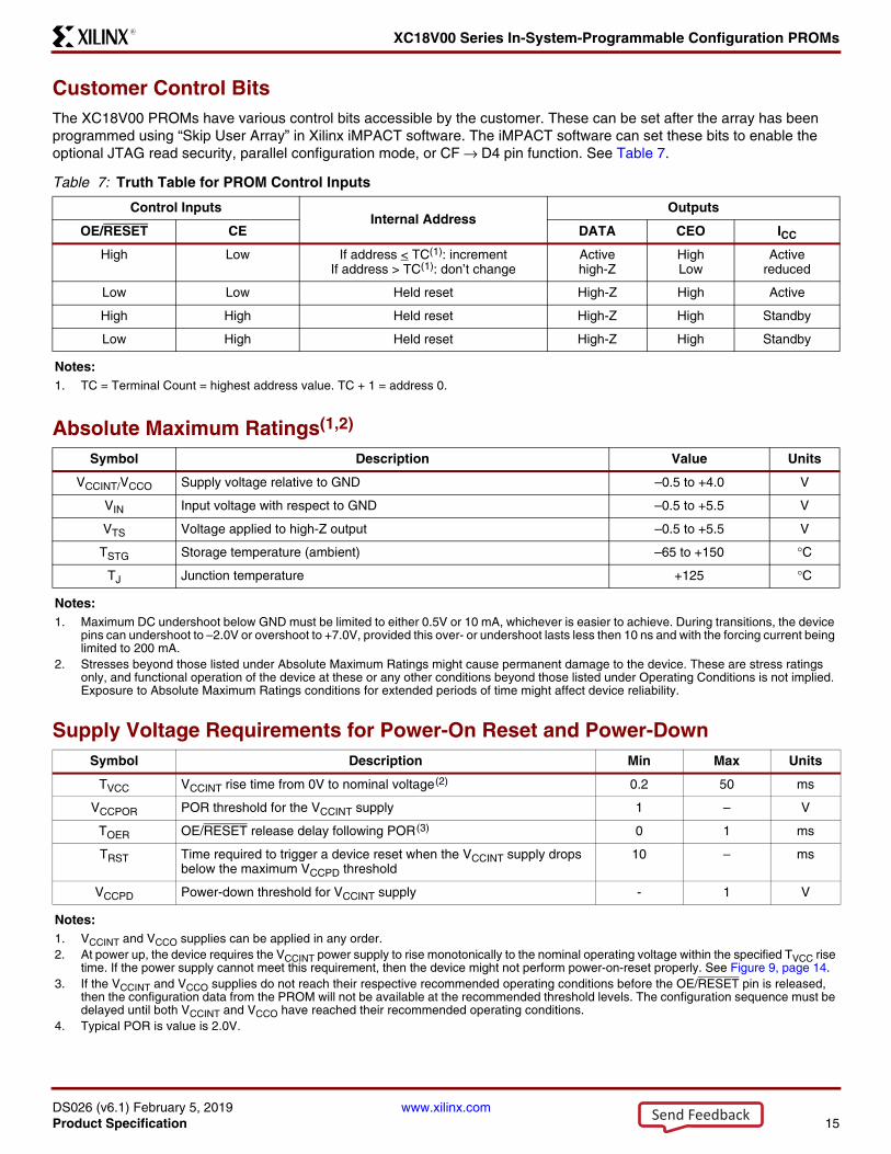
Customer Control BitsThe XC18V00 PROMs have various control bits accessible by the customer. These can be set after the array has been programmed using “Skip User Array” in Xilinx iMPACT software. The iMPACT software can set these bits to enable the optional JTAG read security, parallel configuration mode, or CF → D4 pin function. See Table 7.
Absolute Maximum Ratings(1,2)
Supply Voltage Requirements for Power-On Reset and Power-Down
Table 7: Truth Table for PROM Control Inputs
Control InputsInternal Address
Outputs
OE/RESET CE DATA CEO ICC
High Low If address < TC(1): increment If address > TC(1): don’t change
Activehigh-Z
HighLow
Activereduced
Low Low Held reset High-Z High Active
High High Held reset High-Z High Standby
Low High Held reset High-Z High Standby
Notes: 1. TC = Terminal Count = highest address value. TC + 1 = address 0.
Symbol Description Value Units
VCCINT/VCCO Supply voltage relative to GND –0.5 to +4.0 V
VIN Input voltage with respect to GND –0.5 to +5.5 V
VTS Voltage applied to high-Z output –0.5 to +5.5 V
TSTG Storage temperature (ambient) –65 to +150 °C
TJ Junction temperature +125 °C
Notes: 1. Maximum DC undershoot below GND must be limited to either 0.5V or 10 mA, whichever is easier to achieve. During transitions, the device
pins can undershoot to –2.0V or overshoot to +7.0V, provided this over- or undershoot lasts less then 10 ns and with the forcing current being limited to 200 mA.
2. Stresses beyond those listed under Absolute Maximum Ratings might cause permanent damage to the device. These are stress ratings only, and functional operation of the device at these or any other conditions beyond those listed under Operating Conditions is not implied. Exposure to Absolute Maximum Ratings conditions for extended periods of time might affect device reliability.
Symbol Description Min Max Units
TVCC VCCINT rise time from 0V to nominal voltage(2) 0.2 50 ms
VCCPOR POR threshold for the VCCINT supply 1 – V
TOER OE/RESET release delay following POR(3) 0 1 ms
TRST Time required to trigger a device reset when the VCCINT supply drops below the maximum VCCPD threshold
10 – ms
VCCPD Power-down threshold for VCCINT supply - 1 V
Notes: 1. VCCINT and VCCO supplies can be applied in any order.2. At power up, the device requires the VCCINT power supply to rise monotonically to the nominal operating voltage within the specified TVCC rise
time. If the power supply cannot meet this requirement, then the device might not perform power-on-reset properly. See Figure 9, page 14.3. If the VCCINT and VCCO supplies do not reach their respective recommended operating conditions before the OE/RESET pin is released,
then the configuration data from the PROM will not be available at the recommended threshold levels. The configuration sequence must be delayed until both VCCINT and VCCO have reached their recommended operating conditions.
4. Typical POR is value is 2.0V.
Send Feedback

XC18V00 Series In-System-Programmable Configuration PROMs
DS026 (v6.1) February 5, 2019 www.xilinx.comProduct Specification 16
R
Recommended Operating Conditions
Quality and Reliability Characteristics
DC Characteristics Over Operating Conditions
Symbol Parameter Min Max Units
VCCINT Internal voltage supply 3.0 3.6 V
VCCO Supply voltage for output drivers for 3.3V operation 3.0 3.6 V
Supply voltage for output drivers for 2.5V operation 2.3 2.7 V
VIL Low-level input voltage 0 0.8 V
VIH High-level input voltage 2.0 5.5 V
VO Output voltage 0 VCCO V
TVCC VCCINT rise time from 0V to nominal voltage(1) 1 50 ms
TA Operating ambient temperature(2) –40 85 °C
Notes: 1. At power up, the device requires the VCCINT power supply to rise monotonically from 0V to nominal voltage within the specified VCCINT rise
time. If the power supply cannot meet this requirement, then the device might not perform power-on-reset properly. See Figure 9, page 14.2. Covers the industrial temperature range.
Symbol Description Min Max Units
TDR Data retention 20 – Years
NPE Program/erase cycles (Endurance) 20,000 – Cycles
VESD Electrostatic discharge (ESD) 2,000 – Volts
Symbol Parameter Test Conditions Min Max Units
VOH High-level output voltage for 3.3V outputs IOH = –4 mA 2.4 – V
High-level output voltage for 2.5V outputs IOH = –500 μA 90% VCCO – V
VOL Low-level output voltage for 3.3V outputs IOL = 8 mA – 0.4 V
Low-level output voltage for 2.5V outputs IOL = 500 μA – 0.4 V
ICC Supply current, active mode 25 MHz – 25 mA
ICCS Supply current, standby mode – 10 mA
IILJ JTAG pins TMS, TDI, and TDO pull-up current (1) VCCINT = MAXVIN = GND
– 100 μA
IIL Input leakage current VCCINT = MaxVIN = GND or VCCINT
–10 10 μA
IIH Input and output high-Z leakage current VCCINT = MaxVIN = GND or VCCINT
–10 10 μA
CIN Input capacitance VIN = GNDf = 1.0 MHz
– 8 pF
COUTOutput capacitance VOUT = GND
f = 1.0 MHz– 14 pF
Notes: 1. Internal pull-up resistors guarantee valid logic levels at unconnected input pins. These pull-up resistors do not guarantee valid logic levels
when input pins are connected to other circuits.
Send Feedback

XC18V00 Series In-System-Programmable Configuration PROMs
DS026 (v6.1) February 5, 2019 www.xilinx.comProduct Specification 17
R
AC Characteristics Over Operating Conditions for XC18V04 and XC18V02
OE/RESET
CE
CLK
DATATCE
TOE
TLC
TSCE THCE
THOE
TCAC TOH TDF
TOH
THC
DS026_06_012000
TCYC
Symbol Description Min Max Units
TOE OE/RESET to data delay – 10 ns
TCE CE to data delay – 20 ns
TCAC CLK to data delay – 20 ns
TOH Data hold from CE, OE/RESET, or CLK 0 - ns
TDF CE or OE/RESET to data float delay(2) – 25 ns
TCYC Clock periods 50 – ns
TLC CLK Low time(3) 10 – ns
THC CLK High time(3) 10 – ns
TSCE CE setup time to CLK (guarantees proper counting)(3) 25 – ns
THCE CE High time (guarantees counters are reset) 250 – ns
THOE OE/RESET hold time (guarantees counters are reset) 250 – ns
Notes: 1. AC test load = 50 pF.2. Float delays are measured with 5 pF AC loads. Transition is measured at ±200 mV from steady state active levels.3. Guaranteed by design, not tested.4. All AC parameters are measured with VIL = 0.0V and VIH = 3.0V.5. If THCE High < 2 μs, TCE = 2 μs.6. If THOE Low < 2 μs, TOE = 2 μs.
Send Feedback

XC18V00 Series In-System-Programmable Configuration PROMs
DS026 (v6.1) February 5, 2019 www.xilinx.comProduct Specification 18
R
AC Characteristics Over Operating Conditions for XC18V01 and XC18V512
OE/RESET
CE
CLK
DATATCE
TOE
TLC
TSCE THCE
THOE
TCAC TOH TDF
TOH
THC
DS026_06_012000
TCYC
Symbol Description Min Max Units
TOE OE/RESET to data delay – 10 ns
TCE CE to data delay – 15 ns
TCAC CLK to data delay – 15 ns
TOH Data hold from CE, OE/RESET, or CLK 0 – ns
TDF CE or OE/RESET to data float delay(2) – 25 ns
TCYC Clock periods 30 – ns
TLC CLK Low time(3) 10 – ns
THC CLK High time(3) 10 – ns
TSCE CE setup time to CLK (guarantees proper counting)(3) 20 – ns
THCE CE High time (guarantees counters are reset) 250 – ns
THOE OE/RESET hold time (guarantees counters are reset) 250 – ns
Notes: 1. AC test load = 50 pF.2. Float delays are measured with 5 pF AC loads. Transition is measured at ±200 mV from steady state active levels.3. Guaranteed by design, not tested.4. All AC parameters are measured with VIL = 0.0V and VIH = 3.0V.5. If THCE High < 2 μs, TCE = 2 μs.6. If THOE Low < 2 μs, TOE = 2 μs.
Send Feedback

XC18V00 Series In-System-Programmable Configuration PROMs
DS026 (v6.1) February 5, 2019 www.xilinx.comProduct Specification 19
R
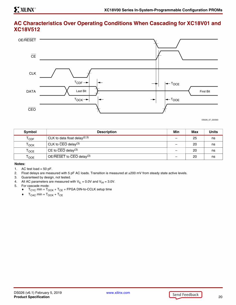
AC Characteristics Over Operating Conditions When Cascading for XC18V04 and XC18V02
CLK
DATA
CE
CEO
First Bit Last Bit
TCDF
DS026_07_020300
OE/RESET
TOCK TOOE
TOCE
Symbol Description Min Max Units
TCDF CLK to data float delay(2,3) – 25 ns
TOCK CLK to CEO delay(3) – 20 ns
TOCE CE to CEO delay(3) – 20 ns
TOOE OE/RESET to CEO delay(3) – 20 ns
Notes: 1. AC test load = 50 pF.2. Float delays are measured with 5 pF AC loads. Transition is measured at ±200 mV from steady state active levels.3. Guaranteed by design, not tested.4. All AC parameters are measured with VIL = 0.0V and VIH = 3.0V.5. For cascade mode:
♦ TCYC min = TOCK + TCE + FPGA DIN-to-CCLK setup time
♦ TCAC min = TOCK + TCE
Send Feedback
XC18V00 Series In-System-Programmable Configuration PROMs
DS026 (v6.1) February 5, 2019 www.xilinx.comProduct Specification 20
R
AC Characteristics Over Operating Conditions When Cascading for XC18V01 and XC18V512
CLK
DATA
CE
CEO
First Bit Last Bit
TCDF
DS026_07_020300
OE/RESET
TOCK TOOE
TOCE
Symbol Description Min Max Units
TCDF CLK to data float delay(2,3) – 25 ns
TOCK CLK to CEO delay(3) – 20 ns
TOCE CE to CEO delay(3) – 20 ns
TOOE OE/RESET to CEO delay(3) – 20 ns
Notes: 1. AC test load = 50 pF.2. Float delays are measured with 5 pF AC loads. Transition is measured at ±200 mV from steady state active levels.3. Guaranteed by design, not tested.4. All AC parameters are measured with VIL = 0.0V and VIH = 3.0V.5. For cascade mode:
♦ TCYC min = TOCK + TCE + FPGA DIN-to-CCLK setup time
♦ TCAC min = TOCK + TCE
Send Feedback
XC18V00 Series In-System-Programmable Configuration PROMs
DS026 (v6.1) February 5, 2019 www.xilinx.comProduct Specification 21
R
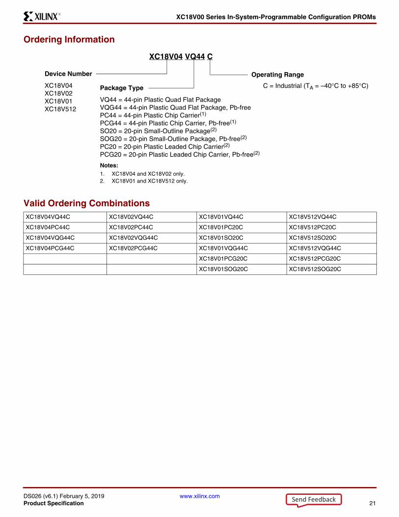
Ordering Information
Valid Ordering CombinationsXC18V04VQ44C XC18V02VQ44C XC18V01VQ44C XC18V512VQ44C
XC18V04PC44C XC18V02PC44C XC18V01PC20C XC18V512PC20C
XC18V04VQG44C XC18V02VQG44C XC18V01SO20C XC18V512SO20C
XC18V04PCG44C XC18V02PCG44C XC18V01VQG44C XC18V512VQG44C
XC18V01PCG20C XC18V512PCG20C
XC18V01SOG20C XC18V512SOG20C
Package Type
VQ44 = 44-pin Plastic Quad Flat PackageVQG44 = 44-pin Plastic Quad Flat Package, Pb-freePC44 = 44-pin Plastic Chip Carrier(1)
PCG44 = 44-pin Plastic Chip Carrier, Pb-free(1)
SO20 = 20-pin Small-Outline Package(2)
SOG20 = 20-pin Small-Outline Package, Pb-free(2)
PC20 = 20-pin Plastic Leaded Chip Carrier(2)
PCG20 = 20-pin Plastic Leaded Chip Carrier, Pb-free(2)
Notes: 1. XC18V04 and XC18V02 only.2. XC18V01 and XC18V512 only.
XC18V04 VQ44 C
Operating Range
C = Industrial (TA = –40°C to +85°C)
Device Number
XC18V04XC18V02XC18V01XC18V512
Send Feedback

XC18V00 Series In-System-Programmable Configuration PROMs
DS026 (v6.1) February 5, 2019 www.xilinx.comProduct Specification 22
R
Marking Information
Package Type
VQ44 = 44-pin Plastic Quad Flat PackageVQG44 = 44-pin Plastic Quad Flat Package, Pb-FreePC44 = 44-pin Plastic Leaded Chip Carrier(1)
PCG44 = 44-pin Plastic Leaded Chip Carrier, Pb-Free(1)
Notes: 1. XC18V02 and XC18V04 only.
20-pin Package(1)
Due to the small size of the serial PROM packages, the complete ordering part number cannot be marked on the package. The package code is simplified. Device marking is as follows:
44-pin PackageXC18V04 VQ44
Operating Range
[no mark] = Industrial (TA = –40°C to +85°C)
Device Number
XC18V04XC18V02XC18V01XC18V512
XC18V01 S
Package Type
S = 20-pin Small-Outline Package(2)
SG = 20-pin Small-Outline Package, Pb-free(2)
J = 20-pin Plastic Leaded Chip Carrier(2)
JG = 20-pin Plastic Leaded Chip Carrier, Pb-free(2)
Notes: 1. Refer to XC18V00 PROM product change notices (PCNs) for legacy part markings.2. XC18V01 and XC18V512 only.
Device Number
18V0118V512
Operating Range
[no mark] = Industrial (TA = –40°C to +85°C)
Send Feedback

XC18V00 Series In-System-Programmable Configuration PROMs
DS026 (v6.1) February 5, 2019 www.xilinx.comProduct Specification 23
R
Revision HistoryThe following table shows the revision history for this document.
Date Version Revision
02/09/1999 1.0 First publication of this early access specification
08/23/1999 1.1 Edited text, changed marking, added CF and parallel load
09/01/1999 1.2 Corrected JTAG order, Security and Endurance data.
09/16/1999 1.3 Corrected SelectMAP diagram, control inputs, reset polarity. Added JTAG and CF description, 256 Kbit and 128 Kbit devices.
01/20/2000 2.0 Added Q44 Package, changed XC18xx to XC18Vxx
02/18/2000 2.1 Updated JTAG configuration, AC and DC characteristics
04/04/2000 2.2 Removed stand alone resistor on INIT pin in Figure 5. Added Virtex-E and EM parts to FPGA table.
06/29/2000 2.3 Removed XC18V128 and updated format. Added AC characteristics for XC18V01, XC18V512, and XC18V256 densities.
11/13/2000 2.4 Features: changed 264 MHz to 264 Mb/s at 33 MHz; AC Spec.: TSCE units to ns, THCE CE High time units to μs. Removed Standby mode statement: “The lower power standby modes available on some XC18V00 devices are set by the user in the programming software”. Changed 10,000 cycles endurance to 20,000 cycles.
01/15/2001 2.5 Updated Figures 5 and 6, added 4.7 resistors. Identification registers: changes ISP PROM product ID from 06h to 26h.
04/04/2001 2.6 Updated Figure 8, Virtex SelectMAP mode; added XC2V products to Compatible PROM table; changed Endurance from 10,000 cycles, 10 years to 20,000, 20 years;
04/30/2001 2.7 Updated Figure 8: removed Virtex-E in Note 2, fixed SelectMAP mode connections. Under "AC Characteristics Over Operating Conditions for XC18V04 and XC18V02", changed TSCE from 25 ms to 25 ns.
06/11/2001 2.8 "AC Characteristics Over Operating Conditions for XC18V01 and XC18V512". Changed Min values for TSCE from 20 ms to 20 ns and for THCE from 2 ms to 2 μs.
09/28/2001 2.9 Changed the Boundary-Scan order for the CEO pin in Table 1, updated the configuration bits values in the table under "Xilinx FPGAs and Compatible PROMs", and added information to the "Recommended Operating Conditions" table.
11/12/2001 3.0 Updated for Spartan-IIE FPGA family.
12/06/2001 3.1 Changed Figure 5(c).
02/27/2002 3.2 Updated Table 2 and Figure 8 for the Virtex-II Pro family of devices.
03/15/2002 3.3 Updated Xilinx software and modified Figure 8 and Figure 5.
03/27/2002 3.4 Made changes to pages 1-3, 5, 7-11, 13, 14, and 18. Added new Figure 9 and Figure 9.
06/14/2002 3.5 Made additions and changes to Table 2.
07/24/2002 3.6 Changed last bullet under Connecting Configuration PROMs, page 9.
09/06/2002 3.7 Multiple minor changes throughout, plus the addition of Pinout Diagrams, page 4 and the deletion of Figure 9.
10/31/2002 3.8 Made minor change on Figure 5 (b) and changed orientation of SO20 diagram on page 5.
11/18/2002 3.9 Added XC2S400E and XC2S600E to Table 2.
04/17/2003 3.10 Changes to "Description", "External Programming", and Table 2.
Send Feedback

XC18V00 Series In-System-Programmable Configuration PROMs
DS026 (v6.1) February 5, 2019 www.xilinx.comProduct Specification 24
R
06/11/2003 4.0 Major revision.• Added alternate IDCODES to Table 5.• Discontinued XC18V256 density.• Eliminated industrial ordering combinations.• Extended commercial temperature range.• Added MultiPRO Desktop Tool support.• Changed THOE and THCE to 250 ns in the tables on <RD Red>page 17 and <RD Red>page 18.• Made change in capacitance values "DC Characteristics Over Operating Conditions".• Added Note (3) to Table 1.• Other minor edits.
12/15/2003 4.1 Added specification (4.7 kΩ) for recommended pull-up resistor on OE/RESET pin to section Reset and Power-On Reset Activation, page 14.Added paragraph to section Standby Mode, page 14, concerning use of a pull-up resistor and/or buffer on the DONE pin.
04/05/2004 5.0 Major revision.• Figure 2: Revised configuration bitstream lengths for most Virtex-II FPGAs.• Replaced previous schematics in Figures 5, 6, 7(a), 7(b), and 7(c) with new Figure 5, Figure 6,
Figure 7, and Figure 8.• Replaced previous Figure 8 with new Figure 9.• Replaced previous power-on text section with new Reset and Power-On Reset Activation,
page 14.• Added specification table Supply Voltage Requirements for Power-On Reset and Power-Down,
page 15.• Added Footnote (5) to:
♦ Specification table AC Characteristics Over Operating Conditions When Cascading for XC18V04 and XC18V02, page 19.
♦ Specification table AC Characteristics Over Operating Conditions When Cascading for XC18V01 and XC18V512, page 20.
• Numerous copyedits and wording changes/clarifications throughout.
07/20/2004 5.0.1 Table 2: Removed reference to XC2VP125 FPGA.
03/06/2006 5.1 • Added Pb-free packages to Features, page 1, Pinout Diagrams, page 4,"Ordering Information", Valid Ordering Combinations, page 21and Marking Information, page 22.
• Removed maximum soldering temperature (TSOL) from Absolute Maximum Ratings(1,2), page 15. Refer to Xilinx Device Package User Guide for package soldering guidelines.
• Added information to Table 5 regarding variable JTAG IDCODE revision field.
01/11/2008 5.2 • Updated document template.• Updated URLs.• Tied RDWR_B and CS_B to GND to ensure valid logic-level Low in FPGA SelectMAP mode in
Figure 6, page 11 and Figure 8, page 13.• Updated "Marking Information," page 22 for 20-pin packaging.
08/05/2015 6.0 This product is obsolete/discontinued per XCN15008. Updated Notice of Disclaimer.
02/05/2019 6.1 The 2015 Product Discontinuation Notice (XCN15008) has been retracted. For more information, see the following Product Discontinuation Notice FAQ (XTP425). Updated Automotive Applications Disclaimer.
Send Feedback

XC18V00 Series In-System-Programmable Configuration PROMs
DS026 (v6.1) February 5, 2019 www.xilinx.comProduct Specification 25
R
Notice of DisclaimerThe information disclosed to you hereunder (the “Materials”) is provided solely for the selection and use of Xilinx products. To themaximum extent permitted by applicable law: (1) Materials are made available "AS IS" and with all faults, Xilinx hereby DISCLAIMS ALLWARRANTIES AND CONDITIONS, EXPRESS, IMPLIED, OR STATUTORY, INCLUDING BUT NOT LIMITED TO WARRANTIES OFMERCHANTABILITY, NON-INFRINGEMENT, OR FITNESS FOR ANY PARTICULAR PURPOSE; and (2) Xilinx shall not be liable(whether in contract or tort, including negligence, or under any other theory of liability) for any loss or damage of any kind or nature relatedto, arising under, or in connection with, the Materials (including your use of the Materials), including for any direct, indirect, special,incidental, or consequential loss or damage (including loss of data, profits, goodwill, or any type of loss or damage suffered as a result ofany action brought by a third party) even if such damage or loss was reasonably foreseeable or Xilinx had been advised of the possibilityof the same. Xilinx assumes no obligation to correct any errors contained in the Materials or to notify you of updates to the Materials or toproduct specifications. You may not reproduce, modify, distribute, or publicly display the Materials without prior written consent. Certainproducts are subject to the terms and conditions of Xilinx’s limited warranty, please refer to Xilinx’s Terms of Sale which can be viewed atwww.xilinx.com/legal.htm#tos; IP cores may be subject to warranty and support terms contained in a license issued to you by Xilinx. Xilinxproducts are not designed or intended to be fail-safe or for use in any application requiring fail-safe performance; you assume sole risk andliability for use of Xilinx products in such critical applications, please refer to Xilinx’s Terms of Sale which can be viewed atwww.xilinx.com/legal.htm#tos.
Automotive Applications DisclaimerAUTOMOTIVE PRODUCTS (IDENTIFIED AS “XA” IN THE PART NUMBER) ARE NOT WARRANTED FOR USE IN THE DEPLOYMENTOF AIRBAGS OR FOR USE IN APPLICATIONS THAT AFFECT CONTROL OF A VEHICLE (“SAFETY APPLICATION”) UNLESS THEREIS A SAFETY CONCEPT OR REDUNDANCY FEATURE CONSISTENT WITH THE ISO 26262 AUTOMOTIVE SAFETY STANDARD(“SAFETY DESIGN”). CUSTOMER SHALL, PRIOR TO USING OR DISTRIBUTING ANY SYSTEMS THAT INCORPORATE PRODUCTS,THOROUGHLY TEST SUCH SYSTEMS FOR SAFETY PURPOSES. USE OF PRODUCTS IN A SAFETY APPLICATION WITHOUT ASAFETY DESIGN IS FULLY AT THE RISK OF CUSTOMER, SUBJECT ONLY TO APPLICABLE LAWS AND REGULATIONSGOVERNING LIMITATIONS ON PRODUCT LIABILITY.
Send Feedback

Mouser Electronics
Authorized Distributor
Click to View Pricing, Inventory, Delivery & Lifecycle Information: Xilinx:
XC18V512SOG20C XC18V01VQG44C0100 XC18V01VQ44C XC18V02PCG44C0100 XC18V04PCG44C
XC18V01VQG44C XC18V512PCG20C XC18V01PCG20C XC18V04VQG44C XC18V01SOG20C XC18V04PC44C
XC18V01SO20C0100 XC18V02PC44C XC18V04VQ44C XC18V02VQG44C XC18V512SO20C
XC18V01PC20C0100 XC18V01PCG20C0100 XC18V01SO20C XC18V512VQG44C XC18V04VQ44C0100
XC18V02PCG44C XC18V01PC20C XC18V512PC20C XC18V512VQ44C XC18V02VQ44C XQ18V04VQ44N