x7r dielectric - used electronic test equipment, spare ... · 13 x7r dielectric specifications and...
TRANSCRIPT
12
0805
Size(L" x W")
5
Voltage4V = 4
6.3V = 610V = Z16V = Y25V = 350V = 5
100V = 1200V = 2500V = 7
C
DielectricX7R = C
103
CapacitanceCode (In pF)2 Sig. Digits +
Number ofZeros
M
CapacitanceToleranceJ = ± 5%K = ±10%M = ± 20%
A
FailureRate
A = NotApplicable
T
TerminationsT = Plated Ni
and Sn7 = Gold
Plated
2
Packaging2 = 7" Reel 4 = 13" Reel7 = Bulk Cass.9 = Bulk
ContactFactory For
Multiples
A
SpecialCode
A = Std.Product
X7R DielectricGeneral Specifications
X7R formulations are called “temperature stable” ceramicsand fall into EIA Class II materials. X7R is the most popularof these intermediate dielectric constant materials. Its tem-perature variation of capacitance is within ±15% from-55°C to +125°C. This capacitance change is non-linear.Capacitance for X7R varies under the influence of electricaloperating conditions such as voltage and frequency.X7R dielectric chip usage covers the broad spectrum ofindustrial applications where known changes in capaci-tance due to applied voltages are acceptable.
PART NUMBER (see page 2 for complete part number explanation)
% C
ap C
hang
e
10
-60 -40 -20 0 20 40 60 80 100 120 140
Temperature °C
X7R DielectricTypical Temperature Coefficient
5
0
-5
-10
-15
-20
-25
%
Cap
acita
nce
+10
+20
+30
0
-10
-20
-301KHz 10 KHz 100 KHz 1 MHz 10 MHz
Frequency
Capacitance vs. Frequency
Insu
latio
n R
esis
tanc
e (O
hm-F
arad
s)
1,000
10,000
100
00 20 12040 60 80
Temperature °C
Insulation Resistance vs Temperature
100
Imp
edan
ce,
10 100 1000
Frequency, MHz
Variation of Impedance with Cap ValueImpedance vs. Frequency
1,000 pF vs. 10,000 pF - X7R0805
0.10
0.01
1.00
1,000 pF
10,000 pF
10.00
Imp
edan
ce,
1 10 100 1,000
Frequency, MHz
Variation of Impedance with Chip SizeImpedance vs. Frequency
100,000 pF - X7R
0.1
.01
1.0
12060805
10
1210
Imp
edan
ce,
1 10 100 1,000
Frequency, MHz
Variation of Impedance with Chip SizeImpedance vs. Frequency
10,000 pF - X7R
0.1
.01
1.0
12060805
10
1210
13
X7R DielectricSpecifications and Test Methods
Parameter/Test X7R Specification Limits Measuring ConditionsOperating Temperature Range -55ºC to +125ºC Temperature Cycle Chamber
Capacitance Within specified tolerance≤ 2.5% for ≥ 50V DC rating Freq.: 1.0 kHz ± 10%
Dissipation Factor ≤ 3.0% for 25V DC rating Voltage: 1.0Vrms ± .2V≤ 3.5% for 16V DC rating For Cap > 10 µF, 0.5Vrms @ 120Hz
≤ 5.0% for ≤ 10V DC rating
Insulation Resistance100,000MΩ or 1000MΩ - µF, Charge device with rated voltage for
whichever is less 120 ± 5 secs @ room temp/humidityCharge device with 300% of rated voltage for
Dielectric Strength No breakdown or visual defects 1-5 seconds, w/charge and discharge currentlimited to 50 mA (max)
Note: Charge device with 150% of ratedvoltage for 500V devices.
Appearance No defects Deflection: 2mmCapacitance Test Time: 30 seconds
Resistance to Variation≤ ±12%
Flexure DissipationMeets Initial Values (As Above)Stresses Factor
Insulation≥ Initial Value x 0.3Resistance
Solderability≥ 95% of each terminal should be covered Dip device in eutectic solder at 230 ± 5ºC
with fresh solder for 5.0 ± 0.5 secondsAppearance No defects, <25% leaching of either end terminalCapacitance
Variation≤ ±7.5%
Dip device in eutectic solder at 260ºC for 60DissipationMeets Initial Values (As Above) seconds. Store at room temperature for 24 ± 2Resistance to Factor hours before measuring electrical properties.Solder Heat InsulationMeets Initial Values (As Above)Resistance
Dielectric Meets Initial Values (As Above)Strength
Appearance No visual defects Step 1: -55ºC ± 2º 30 ± 3 minutesCapacitance
Variation≤ ±7.5% Step 2: Room Temp ≤ 3 minutes
DissipationMeets Initial Values (As Above) Step 3: +125ºC ± 2º 30 ± 3 minutesThermal FactorShock InsulationMeets Initial Values (As Above) Step 4: Room Temp ≤ 3 minutesResistance
Dielectric Meets Initial Values (As Above)
Repeat for 5 cycles and measure afterStrength 24 ± 2 hours at room temperature
Appearance No visual defectsCapacitance
Variation≤ ±12.5%
Dissipation≤ Initial Value x 2.0 (See Above)Load Life Factor
Insulation≥ Initial Value x 0.3 (See Above)Resistance
Dielectric Meets Initial Values (As Above)Strength
Appearance No visual defectsCapacitance
Variation≤ ±12.5%
Load Dissipation≤ Initial Value x 2.0 (See Above)Humidity Factor
Insulation≥ Initial Value x 0.3 (See Above)Resistance
Dielectric Meets Initial Values (As Above)Strength
Charge device with twice rated voltage intest chamber set at 125ºC ± 2ºC
for 1000 hours (+48, -0)
Remove from test chamber and stabilize at room temperature for 24 ± 2 hours
before measuring.
Store in a test chamber set at 85ºC ± 2ºC/85% ± 5% relative humidity for 1000 hours
(+48, -0) with rated voltage applied.
Remove from chamber and stabilize atroom temperature and humidity for
24 ± 2 hours before measuring.
1mm/sec
90 mm
14
X7R DielectricCapacitance Range
PREFERRED SIZES ARE SHADED
SIZE 0201 0402 0603 0805 1206Soldering Reflow Only Reflow Only Reflow Only Reflow/Wave Reflow/WavePackaging All Paper All Paper All Paper Paper/Embossed Paper/Embossed
(L) Length MM 0.60 ± 0.03 1.00 ± 0.10 1.60 ± 0.15 2.01 ± 0.20 3.20 ± 0.20 (in.) (0.024 ± 0.001) (0.040 ± 0.004) (0.063 ± 0.006) (0.079 ± 0.008) (0.126 ± 0.008)
(W) Width MM 0.30 ± 0.03 0.50 ± 0.10 0.81 ± 0.15 1.25 ± 0.20 1.60 ± 0.20(in.) (0.011 ± 0.001) (0.020 ± 0.004) (0.032 ± 0.006) (0.049 ± 0.008) (0.063 ± 0.008)
(t) Terminal MM 0.15 ± 0.05 0.25 ± 0.15 0.35 ± 0.15 0.50 ± 0.25 0.50 ± 0.25(in.) (0.006 ± 0.002) (0.010 ± 0.006) (0.014 ± 0.006) (0.020 ± 0.010) (0.020 ± 0.010)
WVDC 16 16 25 50 6.3 10 16 25 50 100 200 6.3 10 16 25 50 100 200 6.3 10 16 25 50 100 200 500Cap 100 A(pF) 150 A
220 A C330 A C G G G J J J J J J K470 A C G G G J J J J J J K680 A C G G G J J J J J J K
1000 A C G G G J J J J J J K1500 C G G J J J J J J J J J J J J M2200 C G G J J J J J J J J J J J J M3300 C C G G J J J J J J J J J J J J M4700 C G G J J J J J J J J J J J J M6800 C C G G J J J J J J J J J J J J P
Cap 0.010 C G G J J J J J J J J J J J J P(µF 0.015 C G G J J J J J J J J J J J M
0.022 C G G J J J J J N J J J J J M0.033 G G J J J J N J J J J J M0.047 G G G J J J J N J J J J J M0.068 G G G J J J J N J J J J J P0.10 G G G G J J J J N J J J J M0.15 G J J J N J J J J Q0.22 G J J N N J J J J Q0.33 N N N N J J M P Q0.47 N N N N M M M P0.68 N N N M M Q Q1.0 J J N N N M M Q Q1.5 P Q Q2.2 J N Q Q Q3.34.7 P P Q10 P Q Q22 Q47
100WVDC 16 16 25 50 6.3 10 16 25 50 100 200 6.3 10 16 25 50 100 200 6.3 10 16 25 50 100 200 500
SIZE 0201 0402 0603 0805 1206
Letter A C E G J K M N P Q X Y ZMax. 0.33 0.56 0.71 0.86 0.94 1.02 1.27 1.40 1.52 1.78 2.29 2.54 2.79
Thickness (0.013) (0.022) (0.028) (0.034) (0.037) (0.040) (0.050) (0.055) (0.060) (0.070) (0.090) (0.100) (0.110)PAPER EMBOSSED
= Under Development
15
X7R DielectricCapacitance Range
Letter A C E G J K M N P Q X Y ZMax. 0.33 0.56 0.71 0.86 0.94 1.02 1.27 1.40 1.52 1.78 2.29 2.54 2.79
Thickness (0.013) (0.022) (0.028) (0.034) (0.037) (0.040) (0.050) (0.055) (0.060) (0.070) (0.090) (0.100) (0.110)PAPER EMBOSSED
PREFERRED SIZES ARE SHADED
SIZE 1210 1812 1825 2220 2225Soldering Reflow Only Reflow Only Reflow Only Reflow Only Reflow OnlyPackaging Paper/Embossed All Embossed All Embossed All Embossed All Embossed
(L) Length MM 3.20 ± 0.20 4.50 ± 0.30 4.50 ± 0.30 5.70 ± 0.40 5.72 ± 0.25(in.) (0.126 ± 0.008) (0.177 ± 0.012) (0.177 ± 0.012) (0.225 ± 0.016) (0.225 ± 0.010)
(W) Width MM 2.50 ± 0.20 3.20 ± 0.20 6.40 ± 0.40 5.00 ± 0.40 6.35 ± 0.25(in.) (0.098 ± 0.008) (0.126 ± 0.008) (0.252 ± 0.016) (0.197 ± 0.016) (0.250 ± 0.010)
(t) Terminal MM 0.50 ± 0.25 0.61 ± 0.36 0.61 ± 0.36 0.64 ± 0.39 0.64 ± 0.39(in.) (0.020 ± 0.010) (0.024 ± 0.014) (0.024 ± 0.014) (0.025 ± 0.015) (0.025 ± 0.015)
WVDC 10 16 25 50 100 200 500 50 100 200 500 50 100 6.3 50 100 200 50 100Cap 100(pF) 150
220330470680
10001500 J J J J J J M2200 J J J J J J M3300 J J J J J J M4700 J J J J J J M6800 J J J J J J M
Cap 0.010 J J J J J J M K K K K M M X X X X M P(µF 0.015 J J J J J J P K K K P M M X X X X M P
0.022 J J J J J J Q K K K P M M X X X X M P0.033 J J J J J J K K K X M M X X X X M P0.047 J J J J J J K K K Z M M X X X X M P0.068 J J J J J M K K K M M X X X X M P0.10 J J J J J M K K K M M X X X X M P0.15 J J J J M K K P M M X X X X M P0.22 J J J J P K K P M M X X X M P0.33 J J J J Z K M M M X X X M P0.47 M M M M Z K P M M X X X M P0.68 M M P X Z M Q M X X X M P1.0 N N P X Z M X M X Z M P1.5 N N Z Z Z Z M X Z M X2.2 Z Z Z Z Z Z M3.3 Z Z Z Z Z4.7 Z Z Z Z Z10 Z Z Z22 Z Z47
100WVDC 10 16 25 50 100 200 500 50 100 200 500 50 100 6.3 50 100 200 50 100
SIZE 1210 1812 1825 2220 2225
L
W
T
t
= Under Development
60
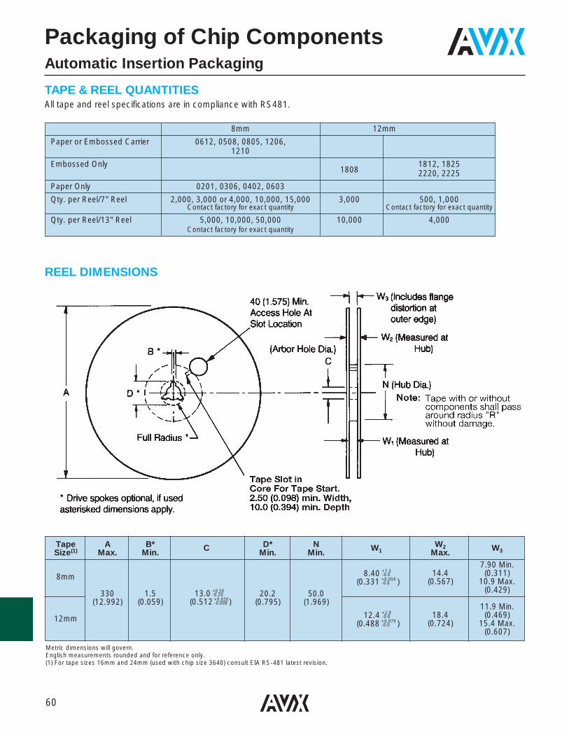
Packaging of Chip ComponentsAutomatic Insertion Packaging
TAPE & REEL QUANTITIESAll tape and reel specifications are in compliance with RS481.
8mm 12mm
Paper or Embossed Carrier 0612, 0508, 0805, 1206,1210
Embossed Only 1812, 18251808 2220, 2225
Paper Only 0201, 0306, 0402, 0603
Qty. per Reel/7" Reel 2,000, 3,000 or 4,000, 10,000, 15,000 3,000 500, 1,000Contact factory for exact quantity Contact factory for exact quantity
Qty. per Reel/13" Reel 5,000, 10,000, 50,000 10,000 4,000Contact factory for exact quantity
REEL DIMENSIONS
Tape A B* C D* N W1W2 W3Size(1) Max. Min. Min. Min. Max.
7.90 Min.8mm 14.4 (0.311)
(0.567) 10.9 Max.330 1.5 20.2 50.0 (0.429)
(12.992) (0.059) (0.795) (1.969) 11.9 Min.12mm 18.4 (0.469)
(0.724) 15.4 Max.(0.607)
Metric dimensions will govern.English measurements rounded and for reference only.(1) For tape sizes 16mm and 24mm (used with chip size 3640) consult EIA RS-481 latest revision.
13.0 +0.50-0.20
(0.512 +0.020)-0.008
8.40 +1.5-0.0
(0.331 +0.059 )-0.0
12.4 +2.0-0.0
(0.488 +0.079 )-0.0
61
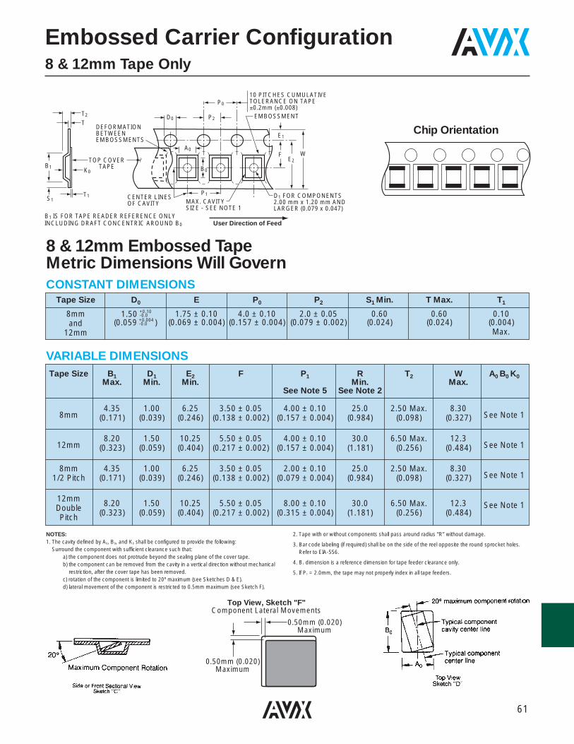
Tape Size B1 D1 E2 F P1 R T2 W A0 B0 K0Max. Min. Min. Min. Max.
See Note 5 See Note 2
8mm4.35 1.00 6.25 3.50 ± 0.05 4.00 ± 0.10 25.0 2.50 Max. 8.30
See Note 1(0.171) (0.039) (0.246) (0.138 ± 0.002) (0.157 ± 0.004) (0.984) (0.098) (0.327)
12mm8.20 1.50 10.25 5.50 ± 0.05 4.00 ± 0.10 30.0 6.50 Max. 12.3
See Note 1(0.323) (0.059) (0.404) (0.217 ± 0.002) (0.157 ± 0.004) (1.181) (0.256) (0.484)
8mm 4.35 1.00 6.25 3.50 ± 0.05 2.00 ± 0.10 25.0 2.50 Max. 8.30See Note 11/2 Pitch (0.171) (0.039) (0.246) (0.138 ± 0.002) (0.079 ± 0.004) (0.984) (0.098) (0.327)
12mm 8.20 1.50 10.25 5.50 ± 0.05 8.00 ± 0.10 30.0 6.50 Max. 12.3 See Note 1Double (0.323) (0.059) (0.404) (0.217 ± 0.002) (0.315 ± 0.004) (1.181) (0.256) (0.484)Pitch
Embossed Carrier Configuration8 & 12mm Tape Only
P0
B0
P1
P2D0T2
T
TOP COVERTAPE
DEFORMATIONBETWEEN EMBOSSMENTS
CENTER LINESOF CAVITY MAX. CAVITY
SIZE - SEE NOTE 1
D1 FOR COMPONENTS2.00 mm x 1.20 mm ANDLARGER (0.079 x 0.047)
10 PITCHES CUMULATIVE TOLERANCE ON TAPE±0.2mm (±0.008)
B1
E1
F
EMBOSSMENT
User Direction of Feed
E2W
K0
T1S1
A0
B1 IS FOR TAPE READER REFERENCE ONLYINCLUDING DRAFT CONCENTRIC AROUND B0
8 & 12mm Embossed TapeMetric Dimensions Will GovernCONSTANT DIMENSIONS
VARIABLE DIMENSIONS
NOTES:1. The cavity defined by A0, B0, and K0 shall be configured to provide the following:
Surround the component with sufficient clearance such that:a) the component does not protrude beyond the sealing plane of the cover tape.b) the component can be removed from the cavity in a vertical direction without mechanical
restriction, after the cover tape has been removed.c) rotation of the component is limited to 20º maximum (see Sketches D & E).d) lateral movement of the component is restricted to 0.5mm maximum (see Sketch F).
2. Tape with or without components shall pass around radius “R” without damage.
3. Bar code labeling (if required) shall be on the side of the reel opposite the round sprocket holes.Refer to EIA-556.
4. B1 dimension is a reference dimension for tape feeder clearance only.
5. If P1 = 2.0mm, the tape may not properly index in all tape feeders.
Tape Size D0 E P0 P2 S1 Min. T Max. T1
8mm 1.75 ± 0.10 4.0 ± 0.10 2.0 ± 0.05 0.60 0.60 0.10and (0.069 ± 0.004) (0.157 ± 0.004) (0.079 ± 0.002) (0.024) (0.024) (0.004)
12mm Max.
0.50mm (0.020)Maximum
0.50mm (0.020)Maximum
Top View, Sketch "F"Component Lateral Movements
1.50 +0.10-0.0
(0.059 +0.004 )-0.0
Chip Orientation
62
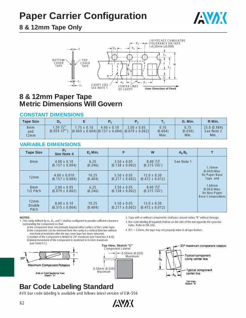
Tape Size P1 E2 Min. F W A0 B0 TSee Note 4
8mm 4.00 ± 0.10 6.25 3.50 ± 0.05 See Note 1(0.157 ± 0.004) (0.246) (0.138 ± 0.002)
12mm 4.00 ± 0.010 10.25 5.50 ± 0.05 12.0 ± 0.30(0.157 ± 0.004) (0.404) (0.217 ± 0.002) (0.472 ± 0.012)
8mm 2.00 ± 0.05 6.25 3.50 ± 0.051/2 Pitch (0.079 ± 0.002) (0.246) (0.138 ± 0.002)
12mm 8.00 ± 0.10 10.25 5.50 ± 0.05 12.0 ± 0.30Double (0.315 ± 0.004) (0.404) (0.217 ± 0.002) (0.472 ± 0.012)Pitch
Paper Carrier Configuration8 & 12mm Tape Only
P0
B0
P1
P2D0T
TOP COVERTAPE
BOTTOM COVERTAPE
CENTER LINESOF CAVITY
CAVITY SIZESEE NOTE 1
10 PITCHES CUMULATIVE TOLERANCE ON TAPE±0.20mm (±0.008)
E1
F
G
User Direction of Feed
E2W
T1
T1 A0
8 & 12mm Paper TapeMetric Dimensions Will GovernCONSTANT DIMENSIONS
Tape Size D0 E P0 P2 T1 G. Min. R Min.
8mm 1.75 ± 0.10 4.00 ± 0.10 2.00 ± 0.05 0.10 0.75 25.0 (0.984)and (0.069 ± 0.004) (0.157 ± 0.004) (0.079 ± 0.002) (0.004) (0.030) See Note 2
12mm Max. Min. Min.
VARIABLE DIMENSIONS
1.10mm (0.043) Max.
for Paper BaseTape and
1.60mm (0.063) Max.
for Non-PaperBase Compositions
NOTES:1. The cavity defined by A0, B0, and T shall be configured to provide sufficient clearance
surrounding the component so that:a) the component does not protrude beyond either surface of the carrier tape;b) the component can be removed from the cavity in a vertical direction without
mechanical restriction after the top cover tape has been removed;c) rotation of the component is limited to 20º maximum (see Sketches A & B);d) lateral movement of the component is restricted to 0.5mm maximum
(see Sketch C).
2. Tape with or without components shall pass around radius “R” without damage.
3. Bar code labeling (if required) shall be on the side of the reel opposite the sprocketholes. Refer to EIA-556.
4. If P1 = 2.0mm, the tape may not properly index in all tape feeders.
0.50mm (0.020)Maximum
0.50mm (0.020)Maximum
Top View, Sketch "C"Component Lateral
1.50 +0.10-0.0
(0.059 +0.004 )-0.0
8.00 +0.30-0.10
(0.315 +0.012 )-0.004
8.00 +0.30-0.10
(0.315 +0.012 )-0.004
Bar Code Labeling StandardAVX bar code labeling is available and follows latest version of EIA-556
63
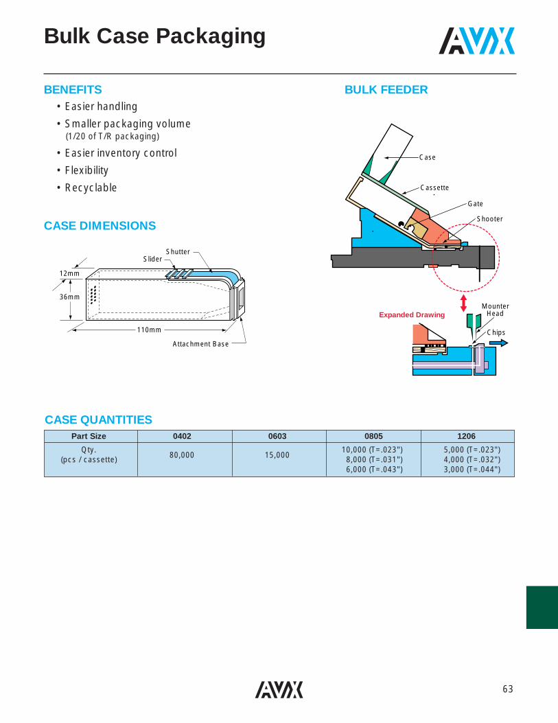
Bulk Case Packaging
CASE QUANTITIESPart Size 0402 0603 0805 1206
Qty. 10,000 (T=.023") 5,000 (T=.023")(pcs / cassette) 80,000 15,000 8,000 (T=.031") 4,000 (T=.032")
6,000 (T=.043") 3,000 (T=.044")
BENEFITS BULK FEEDER• Easier handling
• Smaller packaging volume(1/20 of T/R packaging)
• Easier inventory control
• Flexibility
• Recyclable
CASE DIMENSIONS
ShutterSlider
Attachment Base
110mm
12mm
36mm
Case
Cassette
Gate
Shooter
Chips
Expanded DrawingMounter
Head
64
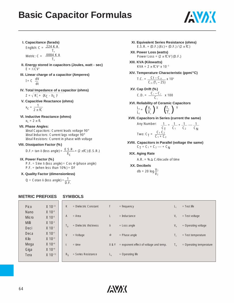
I. Capacitance (farads)
English: C = .224 K A TD
Metric: C = .0884 K ATD
II. Energy stored in capacitors (Joules, watt - sec)E = 1⁄2 CV2
III. Linear charge of a capacitor (Amperes)
I = C dVdt
IV. Total Impedance of a capacitor (ohms)
Z = R2S + (XC - XL )2
V. Capacitive Reactance (ohms)
xc = 12 π fC
VI. Inductive Reactance (ohms)xL = 2 π fL
VII. Phase Angles:Ideal Capacitors: Current leads voltage 90°Ideal Inductors: Current lags voltage 90°Ideal Resistors: Current in phase with voltage
VIII. Dissipation Factor (%)
D.F.= tan (loss angle) = E.S.R. = (2 πfC) (E.S.R.)Xc
IX. Power Factor (%)P.F. = Sine (loss angle) = Cos f (phase angle)P.F. = (when less than 10%) = DF
X. Quality Factor (dimensionless)
Q = Cotan (loss angle) = 1D.F.
XI. Equivalent Series Resistance (ohms)E.S.R. = (D.F.) (Xc) = (D.F.) / (2 π fC)
XII. Power Loss (watts)Power Loss = (2 π fCV2) (D.F.)
XIII. KVA (Kilowatts)KVA = 2 π fCV2 x 10 -3
XIV. Temperature Characteristic (ppm/°C)
T.C. = Ct – C25 x 106
C25 (Tt – 25)
XV. Cap Drift (%)
C.D. = C1 – C2 x 100C1
XVI. Reliability of Ceramic CapacitorsL0 = Vt X Tt YLt
( Vo ) ( To
)XVII. Capacitors in Series (current the same)
Any Number: 1 = 1 + 1 --- 1 CT C1 C2 CN
C1 C2Two: CT =C1 + C2
XVIII. Capacitors in Parallel (voltage the same)CT = C1 + C2 --- + CN
XIX. Aging Rate
A.R. = %D C/decade of time
XX. Decibels
db = 20 log V1
V2
Pico X 10-12
Nano X 10-9
Micro X 10-6
Milli X 10-3
Deci X 10-1
Deca X 10+1
Kilo X 10+3
Mega X 10+6
Giga X 10+9
Tera X 10+12
K = Dielectric Constant f = frequency Lt = Test life
A = Area L = Inductance Vt = Test voltage
TD = Dielectric thickness = Loss angle Vo = Operating voltage
V = Voltage f = Phase angle Tt = Test temperature
t = time X & Y = exponent effect of voltage and temp. To = Operating temperature
Rs = Series Resistance Lo = Operating life
METRIC PREFIXES SYMBOLS
Basic Capacitor Formulas
65
General Description
Formulations – Multilayer ceramic capacitors are availablein both Class 1 and Class 2 formulations. Temperaturecompensating formulation are Class 1 and temperature stable and general application formulations are classified as Class 2.
Class 1 – Class 1 capacitors or temperature compensatingcapacitors are usually made from mixtures of titanateswhere barium titanate is normally not a major part of themix. They have predictable temperature coefficients and in general, do not have an aging characteristic. Thus theyare the most stable capacitor available. The most popularClass 1 multilayer ceramic capacitors are C0G (NP0) temperature compensating capacitors (negative-positive 0 ppm/°C).
Class 2 – EIA Class 2 capacitors typically are based on thechemistry of barium titanate and provide a wide range ofcapacitance values and temperature stability. The mostcommonly used Class 2 dielectrics are X7R and Y5V. TheX7R provides intermediate capacitance values which varyonly ±15% over the temperature range of -55°C to 125°C. Itfinds applications where stability over a wide temperaturerange is required.The Y5V provides the highest capacitance values and isused in applications where limited temperature changes areexpected. The capacitance value for Y5V can vary from22% to -82% over the -30°C to 85°C temperature range.All Class 2 capacitors vary in capacitance value under theinfluence of temperature, operating voltage (both AC andDC), and frequency. For additional information on perfor-mance changes with operating conditions, consult AVX’ssoftware, SpiCap.
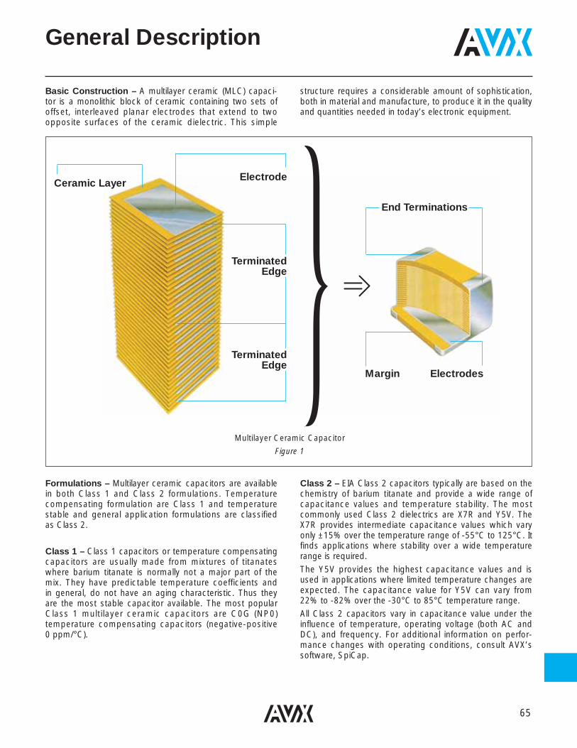
Basic Construction – A multilayer ceramic (MLC) capaci-tor is a monolithic block of ceramic containing two sets ofoffset, interleaved planar electrodes that extend to twoopposite surfaces of the ceramic dielectric. This simple
structure requires a considerable amount of sophistication,both in material and manufacture, to produce it in the qualityand quantities needed in today’s electronic equipment.
Ceramic LayerElectrode
TerminatedEdge
TerminatedEdge
End Terminations
Margin Electrodes
Multilayer Ceramic Capacitor
Figure 1
66
In specifying capacitance change with temperature for Class2 materials, EIA expresses the capacitance change over anoperating temperature range by a 3 symbol code. The firstsymbol represents the cold temperature end of the temper-ature range, the second represents the upper limit of theoperating temperature range and the third symbol repre-sents the capacitance change al lowed over the operating temperature range. Table 1 provides a detailedexplanation of the EIA system.
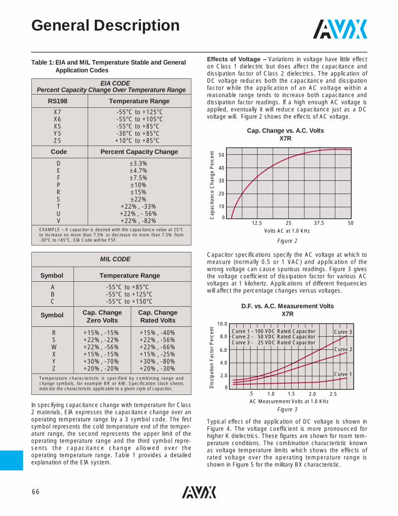
Effects of Voltage – Variations in voltage have little effecton Class 1 dielectric but does affect the capacitance anddissipation factor of Class 2 dielectrics. The application ofDC voltage reduces both the capacitance and dissipationfactor while the application of an AC voltage within a reasonable range tends to increase both capacitance anddissipation factor readings. If a high enough AC voltage isapplied, eventually it will reduce capacitance just as a DCvoltage will. Figure 2 shows the effects of AC voltage.
Capacitor specifications specify the AC voltage at which tomeasure (normally 0.5 or 1 VAC) and application of thewrong voltage can cause spurious readings. Figure 3 givesthe voltage coefficient of dissipation factor for various ACvoltages at 1 kilohertz. Applications of different frequencieswill affect the percentage changes versus voltages.
Typical effect of the application of DC voltage is shown inFigure 4. The voltage coefficient is more pronounced forhigher K dielectrics. These figures are shown for room tem-perature conditions. The combination characteristic knownas voltage temperature limits which shows the effects ofrated voltage over the operating temperature range isshown in Figure 5 for the military BX characteristic.
General Description
Figure 2
50
40
30
20
10
012.5 25 37.5 50
Volts AC at 1.0 KHz
Cap
acita
nce
Cha
nge
Per
cent
Cap. Change vs. A.C. VoltsX7R
Figure 3
Curve 3 - 25 VDC Rated CapacitorCurve 2 - 50 VDC Rated CapacitorCurve 1 - 100 VDC Rated Capacitor Curve 3
Curve 2
Curve 1
.5 1.0 1.5 2.0 2.5AC Measurement Volts at 1.0 KHz
Dis
sip
atio
n Fa
ctor
Per
cent
10.0
8.0
6.0
4.0
2.0
0
D.F. vs. A.C. Measurement VoltsX7R
EIA CODEPercent Capacity Change Over Temperature Range
RS198 Temperature Range
X7 -55°C to +125°CX6 -55°C to +105°CX5 -55°C to +85°CY5 -30°C to +85°CZ5 +10°C to +85°C
Code Percent Capacity Change
D ±3.3%E ±4.7%F ±7.5%P ±10%R ±15%S ±22%T +22%, -33%U +22%, - 56%V +22%, -82%
MIL CODE
Symbol Temperature Range
A -55°C to +85°CB -55°C to +125°CC -55°C to +150°C
Symbol Cap. Change Cap. ChangeZero Volts Rated Volts
R +15%, -15% +15%, -40%S +22%, -22% +22%, -56%W +22%, -56% +22%, -66%X +15%, -15% +15%, -25%Y +30%, -70% +30%, -80%Z +20%, -20% +20%, -30%
Table 1: EIA and MIL Temperature Stable and GeneralApplication Codes
EXAMPLE – A capacitor is desired with the capacitance value at 25°Cto increase no more than 7.5% or decrease no more than 7.5% from -30°C to +85°C. EIA Code will be Y5F.
Temperature characteristic is specified by combining range andchange symbols, for example BR or AW. Specification slash sheetsindicate the characteristic applicable to a given style of capacitor.
67
General Description
Typical Cap. Change vs. D.C. VoltsX7R
Typical Cap. Change vs. TemperatureX7R
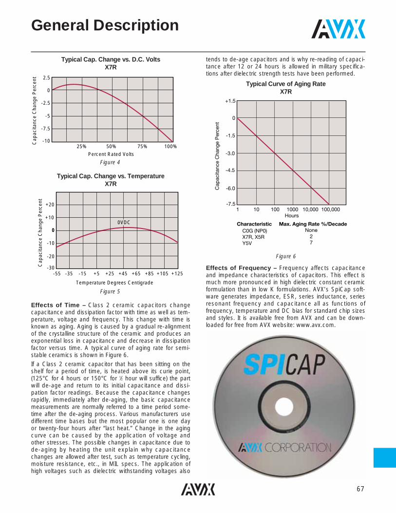
Effects of Time – Class 2 ceramic capacitors changecapacitance and dissipation factor with time as well as tem-perature, voltage and frequency. This change with time isknown as aging. Aging is caused by a gradual re-alignmentof the crystalline structure of the ceramic and produces anexponential loss in capacitance and decrease in dissipationfactor versus time. A typical curve of aging rate for semi-stable ceramics is shown in Figure 6.If a Class 2 ceramic capacitor that has been sitting on theshelf for a period of time, is heated above its curie point,(125°C for 4 hours or 150°C for 1⁄2 hour will suffice) the partwill de-age and return to its initial capacitance and dissi-pation factor readings. Because the capacitance changes rapidly, immediately after de-aging, the basic capacitance measurements are normally referred to a time period some-time after the de-aging process. Various manufacturers usedifferent time bases but the most popular one is one day or twenty-four hours after “last heat.” Change in the agingcurve can be caused by the application of voltage and other stresses. The possible changes in capacitance due tode-aging by heating the unit explain why capacitancechanges are allowed after test, such as temperature cycling,moisture resistance, etc., in MIL specs. The application ofhigh voltages such as dielectric withstanding voltages also
tends to de-age capacitors and is why re-reading of capaci-tance after 12 or 24 hours is allowed in military specifica-tions after dielectric strength tests have been performed.
Effects of Frequency – Frequency affects capacitanceand impedance characteristics of capacitors. This effect ismuch more pronounced in high dielectric constant ceramicformulation than in low K formulations. AVX’s SpiCap soft-ware generates impedance, ESR, series inductance, seriesresonant frequency and capacitance all as functions of frequency, temperature and DC bias for standard chip sizesand styles. It is available free from AVX and can be down-loaded for free from AVX website: www.avx.com.
25% 50% 75% 100%
Percent Rated Volts
Cap
acita
nce
Cha
nge
Per
cent 2.5
0
-2.5
-5
-7.5
-10
0VDC
-55 -35 -15 +5 +25 +45 +65 +85 +105 +125
Temperature Degrees Centigrade
Cap
acita
nce
Cha
nge
Per
cent
+20
+10
0
-10
-20
-30
Figure 4
Figure 5
1 10 100 1000 10,000 100,000 Hours
Cap
acita
nce
Cha
nge
Per
cent
+1.5
0
-1.5
-3.0
-4.5
-6.0
-7.5
Characteristic Max. Aging Rate %/Decade C0G (NP0)X7R, X5RY5V
None27
Figure 6
Typical Curve of Aging RateX7R
68
Effects of Mechanical Stress – High “K” dielectricceramic capacitors exhibit some low level piezoelectricreactions under mechanical stress. As a general statement,the piezoelectric output is higher, the higher the dielectricconstant of the ceramic. It is desirable to investigate thiseffect before using high “K” dielectrics as coupling capaci-tors in extremely low level applications.Reliability – Historically ceramic capacitors have been oneof the most reliable types of capacitors in use today. The approximate formula for the reliability of a ceramiccapacitor is:
Lo = Vt X Tt Y
Lt Vo To
whereLo = operating life Tt = test temperature andLt = test life To = operating temperatureVt = test voltage in °CVo = operating voltage X,Y = see text
Historically for ceramic capacitors exponent X has beenconsidered as 3. The exponent Y for temperature effectstypically tends to run about 8.
A capacitor is a component which is capable of storingelectrical energy. It consists of two conductive plates (elec-trodes) separated by insulating material which is called thedielectric. A typical formula for determining capacitance is:
C = .224 KAt
C = capacitance (picofarads)K = dielectric constant (Vacuum = 1)A = area in square inchest = separation between the plates in inches
(thickness of dielectric).224 = conversion constant
(.0884 for metric system in cm)Capacitance – The standard unit of capacitance is thefarad. A capacitor has a capacitance of 1 farad when 1coulomb charges it to 1 volt. One farad is a very large unitand most capacitors have values in the micro (10-6), nano(10-9) or pico (10-12) farad level.Dielectric Constant – In the formula for capacitance givenabove the dielectric constant of a vacuum is arbitrarily cho-sen as the number 1. Dielectric constants of other materialsare then compared to the dielectric constant of a vacuum.Dielectric Thickness – Capacitance is indirectly propor-tional to the separation between electrodes. Lower voltagerequirements mean thinner dielectrics and greater capaci-tance per volume.Area – Capacitance is directly proportional to the area ofthe electrodes. Since the other variables in the equation areusually set by the performance desired, area is the easiestparameter to modify to obtain a specific capacitance withina material group.
Energy Stored – The energy which can be stored in acapacitor is given by the formula:
E = 1⁄2CV2
E = energy in joules (watts-sec)V = applied voltageC = capacitance in farads
Potential Change – A capacitor is a reactive componentwhich reacts against a change in potential across it. This isshown by the equation for the linear charge of a capacitor:
I ideal = C dVdt
whereI = Current
C = CapacitancedV/dt = Slope of voltage transition across capacitor
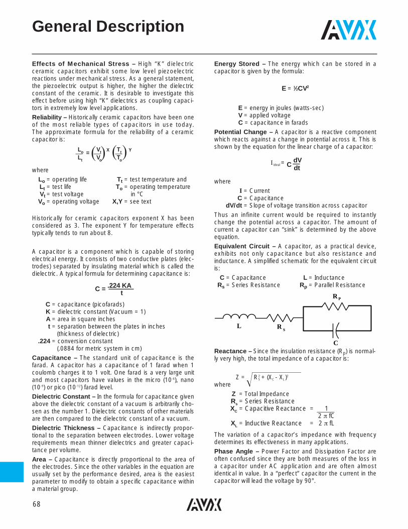
Thus an infinite current would be required to instantlychange the potential across a capacitor. The amount ofcurrent a capacitor can “sink” is determined by the aboveequation.Equivalent Circuit – A capacitor, as a practical device,exhibits not only capacitance but also resistance andinductance. A simplified schematic for the equivalent circuitis:
C = Capacitance L = Inductance Rs = Series Resistance Rp = Parallel Resistance
Reactance – Since the insulation resistance (Rp) is normal-ly very high, the total impedance of a capacitor is:
Z = R2S + (XC - XL)2
whereZ = Total Impedance Rs = Series ResistanceXC = Capacitive Reactance = 1
2 π fCXL = Inductive Reactance = 2 π fL
The variation of a capacitor’s impedance with frequencydetermines its effectiveness in many applications.Phase Angle – Power Factor and Dissipation Factor areoften confused since they are both measures of the loss ina capacitor under AC application and are often almostidentical in value. In a “perfect” capacitor the current in thecapacitor will lead the voltage by 90°.
General Description
R
L R
C
P
S
69
General Description
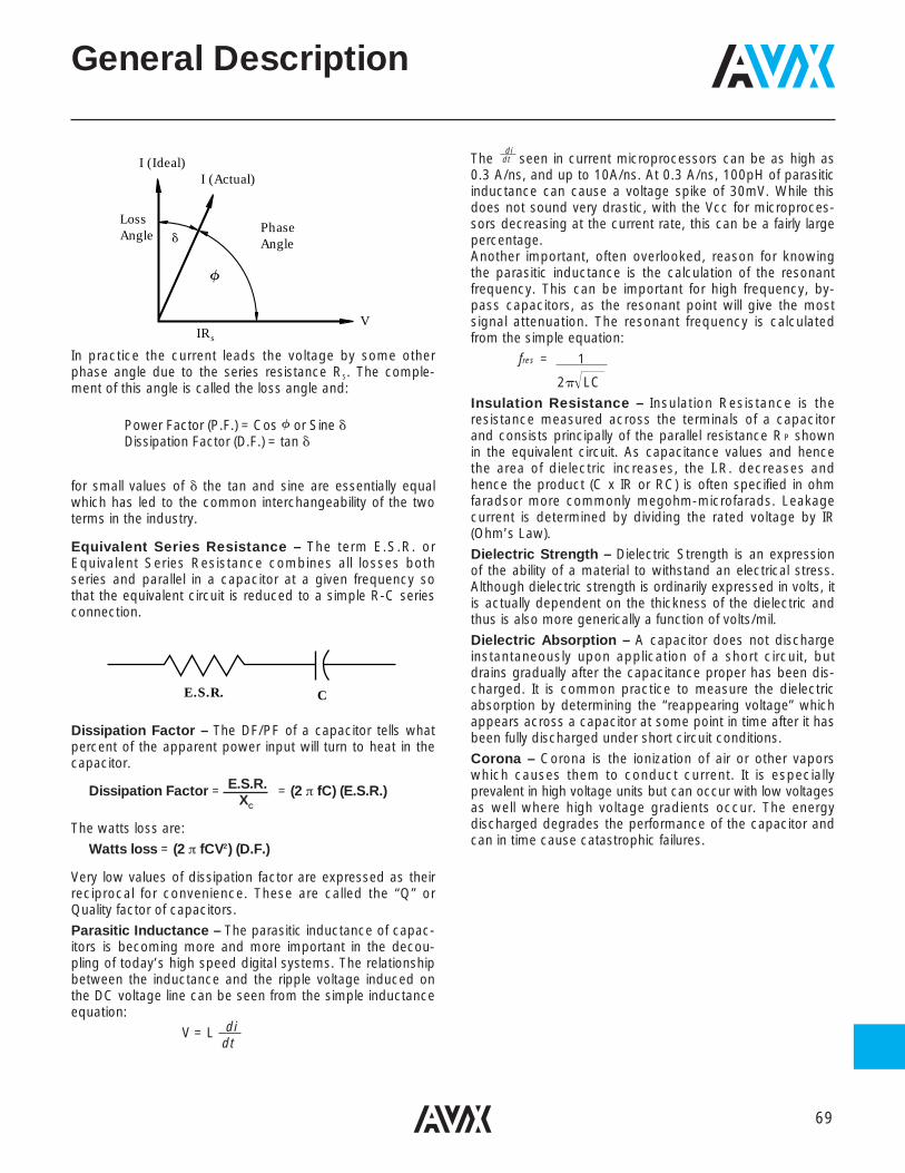
In practice the current leads the voltage by some otherphase angle due to the series resistance RS. The comple-ment of this angle is called the loss angle and:
Power Factor (P.F.) = Cos f or Sine Dissipation Factor (D.F.) = tan
for small values of the tan and sine are essentially equalwhich has led to the common interchangeability of the twoterms in the industry.
Equivalent Series Resistance – The term E.S.R. orEquivalent Series Resistance combines all losses bothseries and parallel in a capacitor at a given frequency sothat the equivalent circuit is reduced to a simple R-C seriesconnection.
Dissipation Factor – The DF/PF of a capacitor tells whatpercent of the apparent power input will turn to heat in thecapacitor.
Dissipation Factor = E.S.R. = (2 π fC) (E.S.R.)XC
The watts loss are:Watts loss = (2 π fCV2) (D.F.)
Very low values of dissipation factor are expressed as theirreciprocal for convenience. These are called the “Q” orQuality factor of capacitors.Parasitic Inductance – The parasitic inductance of capac-itors is becoming more and more important in the decou-pling of today’s high speed digital systems. The relationshipbetween the inductance and the ripple voltage induced onthe DC voltage line can be seen from the simple inductanceequation:
V = L di dt
The seen in current microprocessors can be as high as0.3 A/ns, and up to 10A/ns. At 0.3 A/ns, 100pH of parasiticinductance can cause a voltage spike of 30mV. While thisdoes not sound very drastic, with the Vcc for microproces-sors decreasing at the current rate, this can be a fairly largepercentage.Another important, often overlooked, reason for knowingthe parasitic inductance is the calculation of the resonantfrequency. This can be important for high frequency, by-pass capacitors, as the resonant point will give the mostsignal attenuation. The resonant frequency is calculatedfrom the simple equation:
fres = 1
2 LCInsulation Resistance – Insulation Resistance is the resistance measured across the terminals of a capacitorand consists principally of the parallel resistance RP shownin the equivalent circuit. As capacitance values and hencethe area of dielectric increases, the I.R. decreases andhence the product (C x IR or RC) is often specified in ohmfaradsor more commonly megohm-microfarads. Leakagecurrent is determined by dividing the rated voltage by IR(Ohm’s Law).Dielectric Strength – Dielectric Strength is an expressionof the ability of a material to withstand an electrical stress.Although dielectric strength is ordinarily expressed in volts, itis actually dependent on the thickness of the dielectric andthus is also more generically a function of volts/mil.Dielectric Absorption – A capacitor does not dischargeinstantaneously upon application of a short circuit, butdrains gradually after the capacitance proper has been dis-charged. It is common practice to measure the dielectricabsorption by determining the “reappearing voltage” whichappears across a capacitor at some point in time after it hasbeen fully discharged under short circuit conditions.Corona – Corona is the ionization of air or other vaporswhich causes them to conduct current. It is especiallyprevalent in high voltage units but can occur with low voltagesas well where high voltage gradients occur. The energydischarged degrades the performance of the capacitor andcan in time cause catastrophic failures.
di dt
I (Ideal)I (Actual)
PhaseAngle
LossAngle
VIRs
f
E.S.R. C
70
Surface Mounting GuideMLC Chip Capacitors
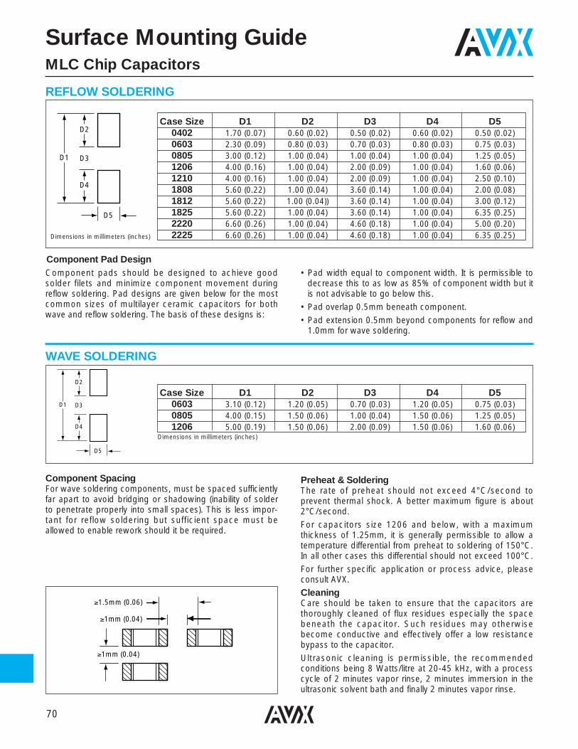
Component pads should be designed to achieve good solder filets and minimize component movement duringreflow soldering. Pad designs are given below for the mostcommon sizes of multilayer ceramic capacitors for bothwave and reflow soldering. The basis of these designs is:
• Pad width equal to component width. It is permissible todecrease this to as low as 85% of component width but itis not advisable to go below this.
• Pad overlap 0.5mm beneath component.• Pad extension 0.5mm beyond components for reflow and
1.0mm for wave soldering.
D1
D2
D3
D4
D5
Case Size D1 D2 D3 D4 D50402 1.70 (0.07) 0.60 (0.02) 0.50 (0.02) 0.60 (0.02) 0.50 (0.02)0603 2.30 (0.09) 0.80 (0.03) 0.70 (0.03) 0.80 (0.03) 0.75 (0.03)0805 3.00 (0.12) 1.00 (0.04) 1.00 (0.04) 1.00 (0.04) 1.25 (0.05)1206 4.00 (0.16) 1.00 (0.04) 2.00 (0.09) 1.00 (0.04) 1.60 (0.06)1210 4.00 (0.16) 1.00 (0.04) 2.00 (0.09) 1.00 (0.04) 2.50 (0.10)1808 5.60 (0.22) 1.00 (0.04) 3.60 (0.14) 1.00 (0.04) 2.00 (0.08)1812 5.60 (0.22) 1.00 (0.04)) 3.60 (0.14) 1.00 (0.04) 3.00 (0.12)1825 5.60 (0.22) 1.00 (0.04) 3.60 (0.14) 1.00 (0.04) 6.35 (0.25)2220 6.60 (0.26) 1.00 (0.04) 4.60 (0.18) 1.00 (0.04) 5.00 (0.20)2225 6.60 (0.26) 1.00 (0.04) 4.60 (0.18) 1.00 (0.04) 6.35 (0.25)Dimensions in millimeters (inches)
REFLOW SOLDERING
WAVE SOLDERING
Component SpacingFor wave soldering components, must be spaced sufficientlyfar apart to avoid bridging or shadowing (inability of solderto penetrate properly into small spaces). This is less impor-tant for reflow soldering but sufficient space must beallowed to enable rework should it be required.
Preheat & SolderingThe rate of preheat should not exceed 4°C/second to prevent thermal shock. A better maximum figure is about2°C/second.For capacitors size 1206 and below, with a maximum thickness of 1.25mm, it is generally permissible to allow atemperature differential from preheat to soldering of 150°C.In all other cases this differential should not exceed 100°C.For further specific application or process advice, pleaseconsult AVX.CleaningCare should be taken to ensure that the capacitors arethoroughly cleaned of flux residues especially the spacebeneath the capacitor. Such residues may otherwisebecome conductive and effectively offer a low resistancebypass to the capacitor.Ultrasonic cleaning is permissible, the recommended conditions being 8 Watts/litre at 20-45 kHz, with a processcycle of 2 minutes vapor rinse, 2 minutes immersion in theultrasonic solvent bath and finally 2 minutes vapor rinse.
D1
D2
D3
D4
D5
Case Size D1 D2 D3 D4 D50603 3.10 (0.12) 1.20 (0.05) 0.70 (0.03) 1.20 (0.05) 0.75 (0.03)0805 4.00 (0.15) 1.50 (0.06) 1.00 (0.04) 1.50 (0.06) 1.25 (0.05)1206 5.00 (0.19) 1.50 (0.06) 2.00 (0.09) 1.50 (0.06) 1.60 (0.06)
Dimensions in millimeters (inches)
≥1mm (0.04)
≥1.5mm (0.06)
≥1mm (0.04)
Component Pad Design
71
Surface Mounting GuideMLC Chip Capacitors
APPLICATION NOTES
StorageGood solderability is maintained for at least twelve months,provided the components are stored in their “as received”packaging at less than 40°C and 70% RH.
SolderabilityTerminations to be well soldered after immersion in a 60/40tin/lead solder bath at 235 ± 5°C for 2 ± 1 seconds.
LeachingTerminations will resist leaching for at least the immersiontimes and conditions shown below.
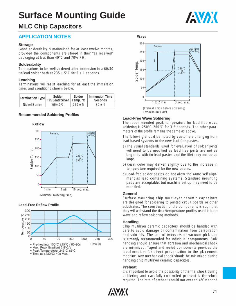
Recommended Soldering Profiles
Lead-Free Reflow Profile
Lead-Free Wave SolderingThe recommended peak temperature for lead-free wave soldering is 250°C-260°C for 3-5 seconds. The other para-meters of the profile remains the same as above.The following should be noted by customers changing fromlead based systems to the new lead free pastes.a) The visual standards used for evaluation of solder joints
will need to be modified as lead free joints are not asbright as with tin-lead pastes and the fillet may not be aslarge.
b) Resin color may darken slightly due to the increase in temperature required for the new pastes.
c) Lead-free solder pastes do not allow the same self align-ment as lead containing systems. Standard mountingpads are acceptable, but machine set up may need to bemodified.
GeneralSurface mounting chip multilayer ceramic capacitors are designed for soldering to printed circuit boards or othersubstrates. The construction of the components is such thatthey will withstand the time/temperature profiles used in bothwave and reflow soldering methods.
HandlingChip multilayer ceramic capacitors should be handled withcare to avoid damage or contamination from perspirationand skin oils. The use of tweezers or vacuum pick ups is strongly recommended for individual components. Bulkhandling should ensure that abrasion and mechanical shockare minimized. Taped and reeled components provides theideal medium for direct presentation to the placementmachine. Any mechanical shock should be minimized duringhandling chip multilayer ceramic capacitors.
PreheatIt is important to avoid the possibility of thermal shock duringsoldering and carefully controlled preheat is thereforerequired. The rate of preheat should not exceed 4°C/second
Termination Type Solder Solder Immersion TimeTin/Lead/Silver Temp. °C Seconds
Nickel Barrier 60/40/0 260 ± 5 30 ± 1
Reflow
300
250
200
150
100
50
0
Sol
der
Tem
p.
10 sec. max1min1min
(Minimize soldering time)
NaturalCooling
220°Cto
250°C
Preheat
Wave
300
250
200
150
100
50
0
Sol
der
Tem
p.
(Preheat chips before soldering)T/maximum 150°C
3 sec. max1 to 2 min
PreheatNaturalCooling
230°Cto
250°C
T
3002502001501005000 50 100 150 200 250 300
• Pre-heating: 150°C ±15°C / 60-90s• Max. Peak Gradient 2.5°C/s• Peak Temperature: 245°C ±5°C• Time at >230°C: 40s Max.
Tem
per
atur
e °C
Time (s)
72
Surface Mounting GuideMLC Chip Capacitorsand a target figure 2°C/second is recommended. Althoughan 80°C to 120°C temperature differential is preferred,recent developments allow a temperature differentialbetween the component surface and the soldering temper-ature of 150°C (Maximum) for capacitors of 1210 size andbelow with a maximum thickness of 1.25mm. The user iscautioned that the risk of thermal shock increases as chipsize or temperature differential increases.
SolderingMildly activated rosin fluxes are preferred. The minimumamount of solder to give a good joint should be used.Excessive solder can lead to damage from the stressescaused by the difference in coefficients of expansionbetween solder, chip and substrate. AVX terminations aresuitable for all wave and reflow soldering systems. If handsoldering cannot be avoided, the preferred technique is theutilization of hot air soldering tools.
CoolingNatural cooling in air is preferred, as this minimizes stresseswithin the soldered joint. When forced air cooling is used,cooling rate should not exceed 4°C/second. Quenching is not recommended but if used, maximum temperature differentials should be observed according to the preheat conditions above.
CleaningFlux residues may be hygroscopic or acidic and must beremoved. AVX MLC capacitors are acceptable for use withall of the solvents described in the specifications MIL-STD-202 and EIA-RS-198. Alcohol based solvents are acceptableand properly controlled water cleaning systems are alsoacceptable. Many other solvents have been proven successful,and most solvents that are acceptable to other componentson circuit assemblies are equally acceptable for use withceramic capacitors.
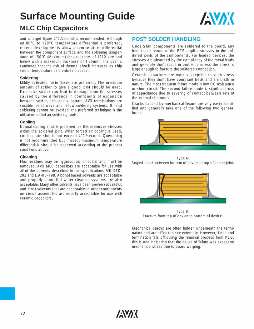
POST SOLDER HANDLINGOnce SMP components are soldered to the board, anybending or flexure of the PCB applies stresses to the sol-dered joints of the components. For leaded devices, thestresses are absorbed by the compliancy of the metal leadsand generally don’t result in problems unless the stress islarge enough to fracture the soldered connection.Ceramic capacitors are more susceptible to such stressbecause they don’t have compliant leads and are brittle innature. The most frequent failure mode is low DC resistanceor short circuit. The second failure mode is significant lossof capacitance due to severing of contact between sets ofthe internal electrodes.Cracks caused by mechanical flexure are very easily identi-fied and generally take one of the following two generalforms:
Mechanical cracks are often hidden underneath the termi-nation and are difficult to see externally. However, if one endtermination falls off during the removal process from PCB,this is one indication that the cause of failure was excessivemechanical stress due to board warping.
Type A: Angled crack between bottom of device to top of solder joint.
Type B: Fracture from top of device to bottom of device.
73
Surface Mounting GuideMLC Chip Capacitors
PCB BOARD DESIGNTo avoid many of the handling problems, AVX recommends that MLCs be located at least .2" away from nearest edge ofboard. However when this is not possible, AVX recommends that the panel be routed along the cut line, adjacent to where theMLC is located.
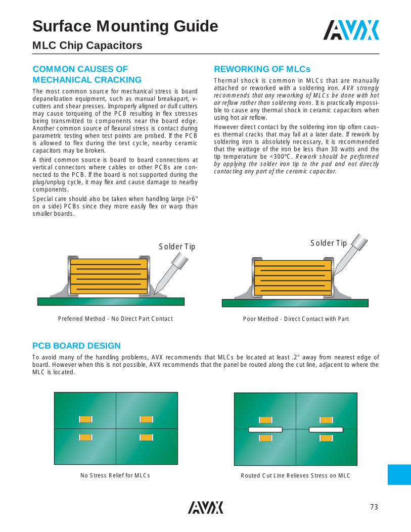
Solder Tip Solder Tip
Preferred Method - No Direct Part Contact Poor Method - Direct Contact with Part
No Stress Relief for MLCs Routed Cut Line Relieves Stress on MLC
COMMON CAUSES OF MECHANICAL CRACKINGThe most common source for mechanical stress is boarddepanelization equipment, such as manual breakapart, v-cutters and shear presses. Improperly aligned or dull cuttersmay cause torqueing of the PCB resulting in flex stressesbeing transmitted to components near the board edge.Another common source of flexural stress is contact duringparametric testing when test points are probed. If the PCBis allowed to flex during the test cycle, nearby ceramiccapacitors may be broken.A third common source is board to board connections atvertical connectors where cables or other PCBs are con-nected to the PCB. If the board is not supported during theplug/unplug cycle, it may flex and cause damage to nearbycomponents.Special care should also be taken when handling large (>6"on a side) PCBs since they more easily flex or warp thansmaller boards.
REWORKING OF MLCsThermal shock is common in MLCs that are manuallyattached or reworked with a soldering iron. AVX stronglyrecommends that any reworking of MLCs be done with hotair reflow rather than soldering irons. It is practically impossi-ble to cause any thermal shock in ceramic capacitors whenusing hot air reflow.However direct contact by the soldering iron tip often caus-es thermal cracks that may fail at a later date. If rework bysoldering iron is absolutely necessary, it is recommendedthat the wattage of the iron be less than 30 watts and thetip temperature be <300ºC. Rework should be performedby applying the solder iron tip to the pad and not directlycontacting any part of the ceramic capacitor.