x5r dielectric, 4 – 50 vdc (commercial grade) level control (alc). the alc feature should be...
TRANSCRIPT
© KEMET Electronics Corporation • P.O. Box 5928 • Greenville, SC 29606 (864) 963-6300 • www.kemet.com C1006_X5R_SMD • 5/7/2012 1One WORLD One Brand One Strategy One Focus One Team One KEMET
Benefits
• -55°C to +85°C operating temperature range• Pb-Free and RoHS Compliant• Temperature stable dielectric• EIA 0201, 0402, 0603, 0805, 1206, and 1210 case sizes• DC voltage ratings of 4 V, 6.3 V, 10 V, 16 V, 25 V, 35 V and 50 V• Capacitance offerings ranging from 0.01 μF to 100 μF• Available capacitance tolerances of ±10% and ±20%• Non-polar device, minimizing installation concerns• 100% pure matte tin-plated termination finish allowing for
excellent solderability
Applications
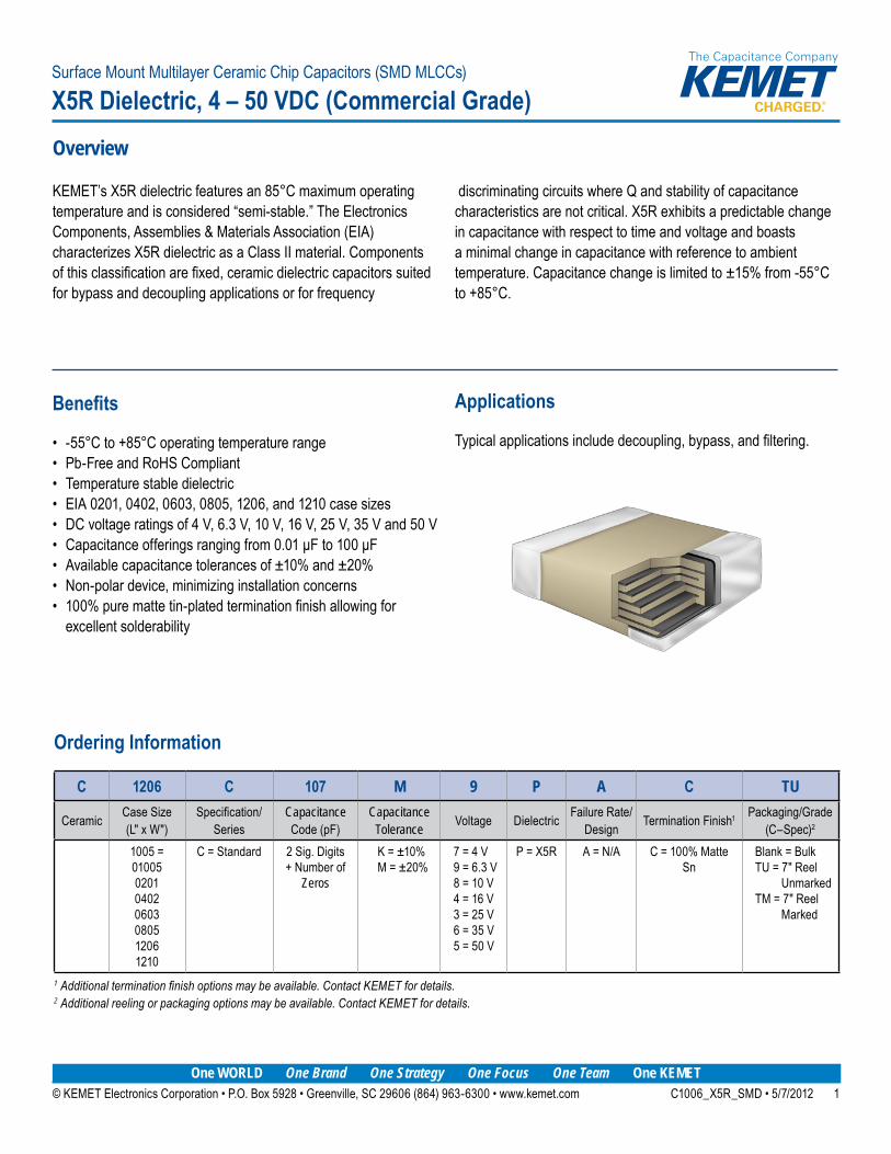
Typical applications include decoupling, bypass, and filtering.
Overview
KEMET’s X5R dielectric features an 85°C maximum operating temperature and is considered “semi-stable.” The Electronics Components, Assemblies & Materials Association (EIA) characterizes X5R dielectric as a Class II material. Components of this classification are fixed, ceramic dielectric capacitors suited for bypass and decoupling applications or for frequency
discriminating circuits where Q and stability of capacitance characteristics are not critical. X5R exhibits a predictable change in capacitance with respect to time and voltage and boasts a minimal change in capacitance with reference to ambient temperature. Capacitance change is limited to ±15% from -55°C to +85°C.
Surface Mount Multilayer Ceramic Chip Capacitors (SMD MLCCs)
X5R Dielectric, 4 – 50 VDC (Commercial Grade)
Ordering Information
C 1206 C 107 M 9 P A C TU
Ceramic Case Size (L" x W")
Specification/Series
Capacitance Code (pF)
Capacitance Tolerance Voltage Dielectric Failure Rate/
Design Termination Finish1 Packaging/Grade (C–Spec)2
1005 = 01005020104020603080512061210
C = Standard 2 Sig. Digits + Number of
Zeros
K = ±10%M = ±20%
7 = 4 V9 = 6.3 V8 = 10 V4 = 16 V3 = 25 V6 = 35 V5 = 50 V
P = X5R A = N/A C = 100% Matte Sn
Blank = BulkTU = 7" Reel
UnmarkedTM = 7" Reel
Marked
1 Additional termination finish options may be available. Contact KEMET for details. 2 Additional reeling or packaging options may be available. Contact KEMET for details.

© KEMET Electronics Corporation • P.O. Box 5928 • Greenville, SC 29606 (864) 963-6300 • www.kemet.com C1006_X5R_SMD • 5/7/2012 2
Surface Mount Multilayer Ceramic Chip Capacitors (SMD MLCCs) – X5R Dielectric, 4 – 50 VDC (Commercial Grade)
Dimensions – Millimeters (Inches)
Qualification/Certification
Commercial grade products are subject to internal qualification. Details regarding test methods and conditions are referenced in Table 4, Performance & Reliability.
Environmental Compliance
Pb-Free and RoHS Compliant.
Cer
amic
Su
rfac
e M
ou
nt
W L
T B
S
100% Tin or SnPb Plate
Nickel Plate
Conductive MetalizationElectrodes
EIA Size Code
Metric Size Code
L Length
W Width
T Thickness
B Bandwidth
SSeparation Minimum
Mounting Technique
01005 0402 0.40 (.016) ± 0.02 (.001) 0.20 (.008) ± 0.02 (.001)
See Table 2 for Thickness
0.10 (.004) ± 0.03 (.001)N/A
Solder Reflow Only0201 0603 0.60 (.024) ± 0.03 (.001) 0.30 (.012) ± 0.03 (.001) 0.15 (.006) ± 0.05 (.002)0402 1005 1.00 (.040) ± 0.05 (.002) 0.50 (.020) ± 0.05 (.002) 0.30 (.012) ± 0.10 (.004) 0.30 (.012)0603 1608 1.60 (.063) ± 0.15 (.006) 0.80 (.032) ± 0.15 (.006) 0.35 (.014) ± 0.15 (.006) 0.70 (.028)
Solder Wave or Solder Reflow0805 2012 2.00 (.079) ± 0.20 (.008) 1.25 (.049) ± 0.20 (.008) 0.50 (0.02) ± 0.25 (.010) 0.75 (.030)
1206 3216 3.20 (.126) ± 0.20 (.008) 1.60 (.063) ± 0.20 (.008) 0.50 (0.02) ± 0.25 (.010)
N/A
1210 3225 3.20 (.126) ± 0.20 (.008) 2.50 (.098) ± 0.20 (.008) 0.50 (0.02) ± 0.25 (.010)
Solder Reflow Only1812 4532 4.50 (.177) ± 0.30 (.012) 3.20 (.126) ± 0.30 (.012) 0.60 (.024) ± 0.35 (.014)1825 4564 4.50 (.177) ± 0.30 (.012) 6.40 (.252) ± 0.40 (.016) 0.60 (.024) ± 0.35 (.014)2220 5650 5.70 (.224) ± 0.40 (.016) 5.00 (.197) ± 0.40 (.016) 0.60 (.024) ± 0.35 (.014)2225 5664 5.60 (.220) ± 0.40 (.016) 6.40 (.248) ± 0.40 (.016) 0.60 (.024) ± 0.35 (.014)

© KEMET Electronics Corporation • P.O. Box 5928 • Greenville, SC 29606 (864) 963-6300 • www.kemet.com C1006_X5R_SMD • 5/7/2012 3
Surface Mount Multilayer Ceramic Chip Capacitors (SMD MLCCs) – X5R Dielectric, 4 – 50 VDC (Commercial Grade)
Electrical Parameters/Characteristics
Item Parameters/CharacteristicsOperating Temperature Range -55°C to +85°C
Capacitance Change with Reference to +25°C and 0 VDC Applied (TCC) ±15%
Aging Rate (Maximum % Cap Loss/Decade Hour) 4.0%
Dielectric Withstanding Voltage 250% of rated voltage(5 ±1 seconds and charge/discharge not exceeding 50 mA)
Dissipation Factor (DF) Maximum Limits @ 25ºC See Dissipation Factor Limit Table
Insulation Resistance (IR) Limit @ 25°C See Insulation Resistance Limit Table(Rated voltage applied for 120 ±5 seconds @ 25°C)
Regarding aging rate: Capacitance measurements (including tolerance) are indexed to a referee time of 48 or 1,000 hours. Please refer to a part number specific datasheet for referee time details. To obtain IR limit, divide MΩ-µF value by the capacitance and compare to GΩ limit. Select the lower of the two limits.Capacitance and dissipation factor (DF) measured under the following conditions: 1 kHz ±50 Hz and 1.0 ±0.2 Vrms if capacitance ≤ 10 µF 120 Hz ±10 Hz and 0.5 ±0.1 Vrms if capacitance > 10 µFNote: When measuring capacitance it is important to ensure the set voltage level is held constant. The HP4284 and Agilent E4980 have a feature known as Automatic Level Control (ALC). The ALC feature should be switched to "ON."
Post Environmental Limits
High Temperature Life, Biased Humidity, Moisture Resistance
Dielectric Rated DCVoltage
CapacitanceValue
Dissipation Factor (Maximum %)
CapacitanceShift
Insulation Resistance
X5R
> 25All
3.0
±20% 10% of Initial Limit25 7.5
< 25 < 0.56 µF 7.5
< 25 ≥ 0.56 µF 12.0
Dissipation Factor Limit Table
Rated DC Voltage Capacitance Dissipation Factor 50 – 200 V All 3%
25 V All 5%< 25 V < 0.56 µF 5%< 25 V ≥ 0.56 µF 10%

© KEMET Electronics Corporation • P.O. Box 5928 • Greenville, SC 29606 (864) 963-6300 • www.kemet.com C1006_X5R_SMD • 5/7/2012 4
Surface Mount Multilayer Ceramic Chip Capacitors (SMD MLCCs) – X5R Dielectric, 4 – 50 VDC (Commercial Grade)
Insulation Resistance Limit Table
EIA Case Size 1,000 Megohm Microfarads or 100 GΩ
500 Megohm Microfarads or 10 GΩ
0201 N/A ALL
0402 < .012 µF ≥ .012 µF
0603 < .047 µF ≥ .047 µF
0805 < .047 µF ≥ .047 µF
1206 < 0.22 µF ≥ 0.22 µF
1210 < 0.39 µF ≥ 0.39 µF
1808 ALL N/A
1812 < 2.2 µF ≥ 2.2 µF
1825 ALL N/A
2220 < 10 µF ≥ 10 µF
2225 ALL N/A

© KEMET Electronics Corporation • P.O. Box 5928 • Greenville, SC 29606 (864) 963-6300 • www.kemet.com C1006_X5R_SMD • 5/7/2012 5
Surface Mount Multilayer Ceramic Chip Capacitors (SMD MLCCs) – X5R Dielectric, 4 – 50 VDC (Commercial Grade)
Table 1 – Capacitance Range/Selection Waterfall (1005 – 1210 Case Sizes)
Cap Cap Code
Series C1005 C0201 C0402 C0603 C0805 C1206 C1210Voltage Code 7 9 7 9 8 4 7 9 8 4 3 5 7 9 8 4 3 5 7 9 8 4 3 5 9 8 4 3 1 9 8 4 3 6 5
Voltage DC 4 6.3 4 6.3 10 16 4 6.3 10 16 25 50 4 6.3 10 16 25 50 4 6.3 10 16 25 50 6.3 10 16 25 50 6.3 10 16 25 35 50
Cap Tolerance Product Availability and Chip Thickness Codes - See Table 2 for Chip Thickness Dimensions10,000 pF 103 K M AB AB AB AB 12,000 pF 123 K M BB BB BB BB15,000 pF 153 K M BB BB BB BB18,000 pF 183 K M BB BB BB BB22,000 pF 223 K M BB BB BB BB27,000 pF 273 K M BB BB BB BB33,000 pF 333 K M BB BB BB BB39,000 pF 393 K M BB BB BB BB47,000 pF 473 K M BB BB BB BB56,000 pF 563 K M BB BB BB BB68,000 pF 683 K M BB BB BB BB82,000 pF 823 K M BB BB BB BB
0.10 uF 104 K M AB AB BB BB BB BB0.12 uF 124 K M0.15 uF 154 K M0.18 uF 184 K M0.22 uF 224 K M BB BB 0.27 uF 274 K M CC CC CC CC EB EB EB EB0.33 uF 334 K M CC CC CC CC EB EB EB EB0.39 uF 394 K M CC CC CC CC EB EB EB EB FD FD FD FD FD0.47 uF 474 K M BB BB CC CC CC CC DC DC DC DC DC EC EC EC EC FD FD FD FD FD0.56 uF 564 K M CC CC CC CC DD DD DD DD DD ED ED ED ED FD FD FD FD FD0.68 uF 684 K M CC CC CC CC DE DE DE DE DE EE EE EE EE FD FD FD FD FD0.82 uF 824 K M CC CC CC CC DF DF DF DF DF EF EF EF EF FF FF FF FF FF1.0 uF 105 K M BB BB CC CC CC CC CC DG DG DG DG DG DG EE EE EE EH FH FH FH FH FH FH 1.2 uF 125 K M DC DC DC DC EC EC EC EC FD FD FD FD1.5 uF 155 K M DC DC DC DC EC EC EC EC FD FD FD FD1.8 uF 185 K M DD DD DD DD EC EC EC EC FD FD FD FD2.2 uF 225 K M BB¹ BB¹ CC CC CC CC DG DG DG DG EE EE EE EE FG FG FG FG2.7 uF 275 K M DL DL DL DL EF EF EF EF FG FG FG FG3.3 uF 335 K M BB¹ CC¹ CC¹ DL DL DL DG EH EH EH EH FH FH FH FH3.9 uF 395 K M DG DG DG DG EH EH EH EH FJ FJ FJ FJ4.7 uF 475 K M BC¹ CC CC CC DG DG DH DH DG EH EH EH EH EH FK FK FK FK5.6 uF 565 K M DG DG DG EK EK EH FG FG FG FE6.8 uF 685 K M DG DG DG EK EK EH FJ FJ FJ FJ8.2 uF 825 K M ED ED EH FK FK FK FG10 uF 106 K M CC¹ CC¹ DG DG DG DG EH EH EH EH FK FK FK FH12 uF 126 K M FD¹ FD FG15 uF 156 K M FF FF FG18 uF 186 K M FG FG FH22 uF 226 K M DG¹ DG¹ EH¹ EH¹ FH FH FJ FS¹27 uF 276 K M33 uF 336 K M39 uF 396 K M47 uF 476 K M DH¹ DG¹ EH¹ EH¹ FS¹ FS¹ FS¹
100 uF 107 K M EH¹ FS¹
Cap Cap Code
Voltage DC 4 6.3 4 6.3 10 16 4 6.3 10 16 25 50 4 6.3 10 16 25 50 4 6.3 10 16 25 50 6.3 10 16 25 50 6.3 10 16 25 35 50
Voltage Code 7 9 7 9 8 4 7 9 8 3 5 4 7 9 8 4 3 5 7 9 8 4 3 5 9 8 4 3 5 9 8 4 3 6 5
Series C1005 C0201 C0402 C0603 C0805 C1206 C1210
xx¹ Available only in M tolerance.

© KEMET Electronics Corporation • P.O. Box 5928 • Greenville, SC 29606 (864) 963-6300 • www.kemet.com C1006_X5R_SMD • 5/7/2012 6
Surface Mount Multilayer Ceramic Chip Capacitors (SMD MLCCs) – X5R Dielectric, 4 – 50 VDC (Commercial Grade)
Table 2 – Chip Thickness/Packaging Quantities
Thickness Code
Case Size
Thickness ± Range (mm)
Paper Quantity Plastic Quantity7" Reel 13" Reel 7" Reel 13" Reel
AB 0201 0.30 ± 0.03 15,000 0 0 0 BB 0402 0.50 ± 0.05 10,000 50,000 0 0 BC 0402 0.50 ± 0.05 10,000 50,000 0 0 BB 0402 0.50 ± 0.05 10,000 50,000 0 0 CC 0603 0.80 ± 0.10 4,000 10,000 0 0 DG 0805 0.60 ± 0.10 4,000 10,000 0 0 DH 0805 0.60 ± 0.10 4,000 10,000 0 0 DG 0805 0.60 ± 0.10 4,000 10,000 0 0 DC 0805 0.78 ± 0.10 4,000 10,000 0 0 DD 0805 0.90 ± 0.10 4,000 10,000 0 0 DL 0805 0.95 ± 0.10 0 0 4,000 10,000 DE 0805 1.00 ± 0.10 0 0 2,500 10,000 DF 0805 1.10 ± 0.10 0 0 2,500 10,000 EB 1206 0.78 ± 0.10 4,000 10,000 4,000 10,000 EH 1206 0.78 ± 0.10 4,000 10,000 4,000 10,000 EH 1206 0.78 ± 0.10 4,000 10,000 4,000 10,000 EK 1206 0.80 ± 0.10 0 0 2,000 8,000 EC 1206 0.90 ± 0.10 0 0 4,000 10,000 ED 1206 1.00 ± 0.10 0 0 2,500 10,000 EE 1206 1.10 ± 0.10 0 0 2,500 10,000 EF 1206 1.20 ± 0.15 0 0 2,500 10,000 FH 1210 0.78 ± 0.10 0 0 4,000 10,000 FS 1210 0.78 ± 0.10 0 0 4,000 10,000 FT 1210 0.78 ± 0.10 0 0 4,000 10,000 FD 1210 0.95 ± 0.10 0 0 4,000 10,000 FE 1210 1.00 ± 0.10 0 0 2,500 10,000 FF 1210 1.10 ± 0.10 0 0 2,500 10,000 FG 1210 1.25 ± 0.15 0 0 2,500 10,000 FJ 1210 1.85 ± 0.20 0 0 2,000 8,000 FK 1210 2.10 ± 0.20 0 0 2,000 8,000
Thickness Code
Case Size
Thickness ± Range (mm)
7" Reel 13" Reel 7" Reel 13" Reel
Paper Quantity Plastic Quantity
Package quantity based on finished chip thickness specifications.

© KEMET Electronics Corporation • P.O. Box 5928 • Greenville, SC 29606 (864) 963-6300 • www.kemet.com C1006_X5R_SMD • 5/7/2012 7
Surface Mount Multilayer Ceramic Chip Capacitors (SMD MLCCs) – X5R Dielectric, 4 – 50 VDC (Commercial Grade)
Table 3 – Chip Capacitor Land Pattern Design Recommendations per IPC–7351
EIA Size Code
Metric Size Code
Density Level A: Maximum (Most)
Land Protrusion (mm)
Density Level B: Median (Nominal)
Land Protrusion (mm)
Density Level C: Minimum (Least)
Land Protrusion (mm)C Y X V1 V2 C Y X V1 V2 C Y X V1 V2
01005 0402 0.33 0.46 0.43 1.60 0.90 0.28 0.36 0.33 1.30 0.70 0.23 0.26 0.23 1.00 0.500201 0603 0.38 0.56 0.52 1.80 1.00 0.33 0.46 0.42 1.50 0.80 0.28 0.36 0.32 1.20 0.600402 1005 0.50 0.72 0.72 2.20 1.20 0.45 0.62 0.62 1.90 1.00 0.40 0.52 0.52 1.60 0.800603 1608 0.90 1.15 1.10 4.00 2.10 0.80 0.95 1.00 3.10 1.50 0.60 0.75 0.90 2.40 1.200805 2012 1.00 1.35 1.55 4.40 2.60 0.90 1.15 1.45 3.50 2.00 0.75 0.95 1.35 2.80 1.701206 3216 1.60 1.35 1.90 5.60 2.90 1.50 1.15 1.80 4.70 2.30 1.40 0.95 1.70 4.00 2.001210 3225 1.60 1.35 2.80 5.65 3.80 1.50 1.15 2.70 4.70 3.20 1.40 0.95 2.60 4.00 2.901808 4520 2.30 1.75 2.30 7.40 3.30 2.20 1.55 2.20 6.50 2.70 2.10 1.35 2.10 5.80 2.401812 4532 2.15 1.60 3.60 6.90 4.60 2.05 1.40 3.50 6.00 4.00 1.95 1.20 3.40 5.30 3.701825 4564 2.15 1.60 6.90 6.90 7.90 2.05 1.40 6.80 6.00 7.30 1.95 1.20 6.70 5.30 7.002220 5650 2.75 1.70 5.50 8.20 6.50 2.65 1.50 5.40 7.30 5.90 2.55 1.30 5.30 6.60 5.602225 5664 2.70 1.70 6.90 8.10 7.90 2.60 1.50 6.80 7.20 7.30 2.50 1.30 6.70 6.50 7.00
Density Level A: For low-density product applications. Recommended for wave solder applications and provides a wider process window for reflow solder processes. KEMET only recommends wave soldering of EIA 0603, 0805 and 1206 case sizes.Density Level B: For products with a moderate level of component density. Provides a robust solder attachment condition for reflow solder processes.Density Level C: For high component density product applications. Before adapting the minimum land pattern variations the user should perform qualification testing based on the conditions outlined in IPC Standard 7351 (IPC–7351).
Soldering Process
Recommended Soldering Technique: • Solder wave or solder reflow for EIA case sizes 0603, 0805 and 1206 • All other EIA case sizes are limited to solder reflow onlyRecommended Soldering Profile: • KEMET recommends following the guidelines outlined in IPC/JEDEC J–STD–020

© KEMET Electronics Corporation • P.O. Box 5928 • Greenville, SC 29606 (864) 963-6300 • www.kemet.com C1006_X5R_SMD • 5/7/2012 8
Surface Mount Multilayer Ceramic Chip Capacitors (SMD MLCCs) – X5R Dielectric, 4 – 50 VDC (Commercial Grade)
Table 4 – Performance & Reliability: Test Methods and Conditions
Stress Reference Test or Inspection MethodTerminal Strength JIS–C–6429 Appendix 1, Note: Force of 1.8 kg for 60 seconds.
Board Flex JIS–C–6429 Appendix 2, Note: 2 mm (min) for all except 3 mm for C0G.
Solderability J–STD–002
Magnification 50 X. Conditions:
a) Method B, 4 hours @ 155°C, dry heat @ 235°C
b) Method B @ 215°C category 3
c) Method D, category 3 @ 260°C
Temperature Cycling JESD22 Method JA–104 1,000 Cycles (-55°C to +125°C), Measurement at 24 hours. +/- 2 hours after test conclusion.
Biased Humidity MIL–STD–202 Method 103Load Humidity: 1,000 hours 85°C/85% RH and Rated Voltage. Add 100 K ohm resistor. Measurement at 24 hours. +/- 2 hours after test conclusion.Low Volt Humidity: 1,000 hours 85°C/85% RH and 1.5 V. Add 100 K ohm resistor. Measurement at 24 hours. +/- 2 hours after test conclusion.
Moisture Resistance MIL–STD–202 Method 106 t = 24 hours/cycle. Steps 7a and 7b not required. Unpowered.Measurement at 24 hours. +/- 2 hours after test conclusion.
Thermal Shock MIL–STD–202 Method 107 -55°C/+125°C. Note: Number of cycles required-300, maximum transfer time-20 seconds, dwell time-15 minutes. Air-Air.
High Temperature Life MIL–STD–202 Method 108/EIA–198 1,000 hours at 125°C (85°C for X5R, Z5U and Y5V) with 2 X rated voltage applied.
Storage Life MIL–STD–202 Method 108 150°C, 0 VDC, for 1,000 hours.
Mechanical Shock MIL–STD–202 Method 213 Figure 1 of Method 213, Condition F.
Resistance to Solvents MIL–STD–202 Method 215 Add aqueous wash chemical, OKEM Clean or equivalent.
Storage and Handling
Ceramic chip capacitors should be stored in normal working environments. While the chips themselves are quite robust in other environments, solderability will be degraded by exposure to high temperatures, high humidity, corrosive atmospheres, and long term storage. In addition, packaging materials will be degraded by high temperature–reels may soften or warp, and tape peel force may increase. KEMET recommends that maximum storage temperature not exceed 40ºC, and maximum storage humidity not exceed 70% relative humidity. Temperature fluctuations should be minimized to avoid condensation on the parts, and atmospheres should be free of chlorine and sulfur bearing compounds. For optimized solderability, chip stock should be used promptly, preferably within 1.5 years of receipt.
Construction
Reference Item MaterialA
Termination System
Finish 100% Matte SnB Barrier Layer NiC Base metal CuD Inner Electrode Ni
E Dielectric Material BaTiO3
Note: Image is exaggerated in order to clearly identify all components of construction.

© KEMET Electronics Corporation • P.O. Box 5928 • Greenville, SC 29606 (864) 963-6300 • www.kemet.com C1006_X5R_SMD • 5/7/2012 9
Surface Mount Multilayer Ceramic Chip Capacitors (SMD MLCCs) – X5R Dielectric, 4 – 50 VDC (Commercial Grade)
Tape & Reel Packaging Information
KEMET offers multilayer ceramic chip capacitors packaged in 8, 12 and 16 mm tape on 7" and 13" reels in accordance with EIA Standard 481. This packaging system is compatible with all tape fed automatic pick and place systems. See Table 2 for details on reeling quantities for commercial chips.
8 mm, 12 mmor 16 mm Carrier Tape
178 mm (7.00")or
330 mm (13.00")
Anti-Static Reel
Embossed Plastic* or Punched Paper Carrier.
Embossment or Punched Cavity
Anti-Static Cover Tape(.10 mm (.004") Max Thickness)
Chip and KPS Orientation in Pocket(except 1825 Commercial, and 1825 and 2225 Military)
*EIA 01005, 0201, 0402 and 0603 case sizes available on punched paper carrier only.
KEMET®
Bar Code Label
Sprocket Holes
Table 5 – Carrier Tape Confi guration (mm)
EIA Case Size Tape Size (W)* Lead Space (P1)*01005 – 0402 8 2
0603 – 1210 8 4
1805 – 1808 12 4
≥ 1812 12 8
KPS 1210 12 8
KPS 1812 & 2220 16 12
Array 0508 & 0612 8 4
*Refer to Figure 1 for W and P1 carrier tape reference locations.*Refer to Table 6 for tolerance specifi cations.

© KEMET Electronics Corporation • P.O. Box 5928 • Greenville, SC 29606 (864) 963-6300 • www.kemet.com C1006_X5R_SMD • 5/7/2012 10
Surface Mount Multilayer Ceramic Chip Capacitors (SMD MLCCs) – X5R Dielectric, 4 – 50 VDC (Commercial Grade)
Figure 1 – Embossed (Plastic) Carrier Tape Dimensions
PoT
F
W
Center Lines of Cavity
Ao
Bo
User Direction of Unreeling
Cover Tape
Ko
B1 is for tape feeder reference only, including draft concentric about B o.
T2
ØD1
ØDo
B1
S1
T1
E1
E2
P1
P2
EmbossmentFor cavity size,see Note 1 Table 5
[10 pitches cumulativetolerance on tape ± 0.2 mm]
Table 6 – Embossed (Plastic) Carrier Tape DimensionsMetric will govern
Constant Dimensions — Millimeters (Inches)
Tape Size D0 D1 Minimum
Note 1 E1 P0 P2 R Reference
Note 2S1 Minimum
Note 3T
Maximum.T1
Maximum.
8 mm
1.5 +0.10/-0.0 (0.059 +0.004/-0.0)
1.0 (0.039)
1.75 ±0.10 (0.069 ±0.004)
4.0 ±0.10 (0.157 ±0.004)
2.0 ±0.05 (0.079 ±0.002)
25.0 (0.984)
0.600 (0.024)
0.600 (0.024)
0.100 (0.004)12 mm
1.5 (0.059)
30 (1.181)
16 mm
Variable Dimensions — Millimeters (Inches)
Tape Size Pitch B1 MaximumNote 4 E2 Minimum F P1 T2 Maximum W Maximum A0,B0 & K0
8 mm Single (4 mm) 4.35 (0.171)
6.25 (0.246)
3.5 ±0.05 (0.138 ±0.002)
4.0 ±0.10(0.157 ±0.004)
2.5 (0.098)
8.3 (0.327)
Note 512 mm Single (4 mm) & Double (8 mm)
8.2 (0.323)
10.25 (0.404)
5.5 ±0.05 (0.217 ±0.002)
8.0 ±0.10 (0.315 ±0.004)
4.6 (0.181)
12.3 (0.484)
16 mm Triple (12 mm) 12.1 (0.476)
14.25 (0.561)
5.5 ±0.05 (0.217 ±0.002)
8.0 ±0.10 (0.315 ±0.004)
4.6 (0.181)
16.3 (0.642)
1. The embossment hole location shall be measured from the sprocket hole controlling the location of the embossment. Dimensions of embossment location and hole location shall be applied independent of each other.
2. The tape with or without components shall pass around R without damage (see Figure 5).3. If S1< 1.0 mm, there may not be enough area for cover tape to be properly applied (see EIA Standard 481 paragraph 4.3 section b).4. B1 dimension is a reference dimension for tape feeder clearance only.5. The cavity defi ned by A0, B0 and K0 shall surround the component with suffi cient clearance that: (a) the component does not protrude above the top surface of the carrier tape. (b) the component can be removed from the cavity in a vertical direction without mechanical restriction, after the top cover tape has been removed. (c) rotation of the component is limited to 20° maximum for 8 and 12 mm tapes and 10° maximum for 16 mm tapes (see Figure 3). (d) lateral movement of the component is restricted to 0.5 mm maximum for 8 and 12 mm wide tape and to 1.0 mm maximum for 16 mm tape (see Figure 4). (e) for KPS Series product, A0 and B0 are measured on a plane 0.3 mm above the bottom of the pocket. (f) see Addendum in EIA Standard 481 for standards relating to more precise taping requirements.

© KEMET Electronics Corporation • P.O. Box 5928 • Greenville, SC 29606 (864) 963-6300 • www.kemet.com C1006_X5R_SMD • 5/7/2012 11
Surface Mount Multilayer Ceramic Chip Capacitors (SMD MLCCs) – X5R Dielectric, 4 – 50 VDC (Commercial Grade)
Figure 2 – Punched (Paper) Carrier Tape Dimensions
User Direction of Unreeling
Top Cover Tape
T
Center Lines of Cavity
P1
ØDo PoP2
E1
F
E2W
G
A0
B0
Cavity Size,SeeNote 1, Table 7
Bottom Cover Tape
T1
T1
Bottom Cover Tape
[10 pitches cumulativetolerance on tape ± 0.2 mm]
Table 7 – Punched (Paper) Carrier Tape Dimensions Metric will govern
Constant Dimensions — Millimeters (Inches)Tape Size D0 E1 P0 P2 T1Max G Minimum R Ref.
Note 2
8 mm 1.5 +0.10 -0.0 (0.059 +0.004 -0.0)
1.75 ±0.10 (0.069 ±0.004)
4.0 ±0.10 (0.157 ±0.004)
2.0 ±0.05 (0.079 ±0.002)
0.10 (0.004) Maximum
0.75 (0.030)
25 (0.984)
Variable Dimensions — Millimeters (Inches)Tape Size Pitch E2 Minimum F P1 T Maximum W Maximum A0 B0
8 mm Half (2 mm) 6.25 (0.246)
3.5 ±0.05 (0.138 ±0.002)
2.0 ±0.05 (0.079 ±0.002) 1.1
(0.098)
8.3(0.327) Note 1
8 mm Single (4 mm) 4.0 ±0.10 (0.157 ±0.004)
8.3(0.327)
1. The cavity defi ned by A0, B0 and T shall surround the component with suffi cient clearance that: a) the component does not protrude beyond either surface of the carrier tape. b) the component can be removed from the cavity in a vertical direction without mechanical restriction, after the top cover tape has been removed. d) lateral movement of the component is restricted to 0.5 mm maximum (see Figure 4). e) see Addendum in EIA Standard 481 for standards relating to more precise taping requirements.2. The tape with or without components shall pass around R without damage (see Figure 5).

© KEMET Electronics Corporation • P.O. Box 5928 • Greenville, SC 29606 (864) 963-6300 • www.kemet.com C1006_X5R_SMD • 5/7/2012 12
Surface Mount Multilayer Ceramic Chip Capacitors (SMD MLCCs) – X5R Dielectric, 4 – 50 VDC (Commercial Grade)
Packaging Information Performance Notes
1. Cover Tape Break Force: 1.0 Kg minimum.2. Cover Tape Peel Strength: The total peel strength of the cover tape from the carrier tape shall be:
Tape Width Peel Strength8 mm 0.1 to 1.0 Newton (10 to 100 gf)
12 and 16 mm 0.1 to 1.3 Newton (10 to 130 gf)
The direction of the pull shall be opposite the direction of the carrier tape travel. The pull angle of the carrier tape shall be 165° to 180° from the plane of the carrier tape. During peeling, the carrier and/or cover tape shall be pulled at a velocity of 300 ±10 mm/minute.3. Labeling: Bar code labeling (standard or custom) shall be on the side of the reel opposite the sprocket holes. Refer to EIA Standards 556 and 624.
Figure 2 – Maximum Component Rotation
Ao
Bo
°T
°s
Maximum Component RotationTop View
Maximum Component RotationSide View
Tape MaximumWidth (mm) Rotation ( °
T)8,12 20 16-200 10 Tape Maximum
Width (mm) Rotation ( °S)
8,12 20 16-56 1072-200 5
Typical Pocket Centerline
Typical Component Centerline
Figure 3 – Maximum Lateral Movement
0.5 mm maximum0.5 mm maximum
8 mm & 12 mm Tape
1.0 mm maximum1.0 mm maximum
16 mm Tape
Figure 4 – Bending Radius
RRBending
Radius
EmbossedCarrier
PunchedCarrier

© KEMET Electronics Corporation • P.O. Box 5928 • Greenville, SC 29606 (864) 963-6300 • www.kemet.com C1006_X5R_SMD • 5/7/2012 13
Surface Mount Multilayer Ceramic Chip Capacitors (SMD MLCCs) – X5R Dielectric, 4 – 50 VDC (Commercial Grade)
Figure 6 – Reel Dimensions
A D (See Note)
Full Radius,See Note
B (see Note)
Access Hole atSlot Location(Ø 40 mm min.)
If present,tape slot in corefor tape start:2.5 mm min. width x10.0 mm min. depth
W3 (Includes flange distortion at outer edge)
W2 (Measured at hub)
W1 (Measured at hub)
C(Arbor holediameter)
Note: Drive spokes optional; if used, dimensions B and D shall apply.
N
Table 8 – Reel DimensionsMetric will govern
Constant Dimensions — Millimeters (Inches) Tape Size A B Minimum C D Minimum
8 mm 178 ±0.20 (7.008 ±0.008)
or330 ±0.20
(13.000 ±0.008)
1.5 (0.059)
13.0 +0.5/-0.2 (0.521 +0.02/-0.008)
20.2 (0.795)12 mm
16 mm
Variable Dimensions — Millimeters (Inches) Tape Size N Minimum W1 W2 Maximum W3
8 mm
50 (1.969)
8.4 +1.5/-0.0(0.331 +0.059/-0.0)
14.4 (0.567)
Shall accommodate tape width without interference12 mm 12.4 +2.0/-0.0
(0.488 +0.078/-0.0) 18.4
(0.724)
16 mm 16.4 +2.0/-0.0(0.646 +0.078/-0.0)
22.4 (0.882)

© KEMET Electronics Corporation • P.O. Box 5928 • Greenville, SC 29606 (864) 963-6300 • www.kemet.com C1006_X5R_SMD • 5/7/2012 14
Surface Mount Multilayer Ceramic Chip Capacitors (SMD MLCCs) – X5R Dielectric, 4 – 50 VDC (Commercial Grade)
Figure 7 – Tape Leader & Trailer Dimensions
Trailer160 mm minimum,
Carrier Tape
END STARTRound Sprocket Holes
Elongated Sprocket Holes(32 mm tape and wider)
Top Cover Tape
Top Cover Tape
Punched Carrier8 mm & 12 mm only
Embossed Carrier
Components
100 mm Min.Leader
400 mm Minimum,
Figure 8 – Maximum CamberCarrier Tape
Round Sprocket Holes
1 mm maximum, either direction
Straight Edge
250 mm
Elongated sprocket holes(32 mm & wider tapes)

© KEMET Electronics Corporation • P.O. Box 5928 • Greenville, SC 29606 (864) 963-6300 • www.kemet.com C1006_X5R_SMD • 5/7/2012 15
Surface Mount Multilayer Ceramic Chip Capacitors (SMD MLCCs) – X5R Dielectric, 4 – 50 VDC (Commercial Grade)
Figure 9 – Bulk Cassette Packaging (Ceramic Chips Only)Meets Dimensional Requirements IEC-286 and EIAJ 7201Unit mm *Reference
Table 9 – Capacitor Dimensions for Bulk CassetteCassette Packaging – Millimeters
Table 10 – Capacitor MarkingLaser marking is available as an extra-cost option for most KEMET ceramic chips. Such marking is two sided, and includes a K to identify KEMET, followed by two characters (per EIA-198) to identify the capacitance value. Note that marking is not available for any Y5V chip. ln addition, the 0603 marking option is limited to the K only. (Marking Optional – Not Available for 0402 Size)
Example shown is 1,000 pF capacitor
EIA Size Code
Metric Size Code L Length W Width B Bandwidth S Separation
minimum T Thickness Number of Pcs/Cassette
0402 1005 1.0 ± 0.05 0.5 ± 0.05 0.2 to 0.4 0.3 0.5 ± .05 50,000
0603 1608 1.6 ± 0.07 0.8 ± 0.07 0.2 to 0.5 0.7 0.8 ± .07 15,000
110 ± 0.7
31.5
± 00.
2
36 ±
0 0.2
19.0
*
5 0*
10*
53 3* 68
± 0.
18
8 ±
0.1
12.0
± 0
.1
3.0 ± 00.2
2.0 ± 0.10
1.5 ± 00.1
Numeral Alpha Character
Capacitance (pF) For Various Numeral Identifiers9 0 1 2 3 4 5 6 7
A 0.1 1 10 100 1000 10000 100000 1000000 10000000B 0.11 1.1 11 110 1100 11000 110000 1100000 11000000C 0.12 1.2 12 120 1200 12000 120000 1200000 12000000D 0.13 1.3 13 130 1300 13000 130000 1300000 13000000E 0.15 1.5 15 150 1500 15000 150000 1500000 15000000F 0.16 1.6 16 160 1600 16000 160000 1600000 16000000G 0.18 1.8 18 180 1800 18000 180000 1800000 18000000H 0.2 2 20 200 2000 20000 200000 2000000 20000000J 0.22 2.2 22 220 2200 22000 220000 2200000 22000000K 0.24 2.4 24 240 2400 24000 240000 2400000 24000000L 0.27 2.7 27 270 2700 27000 270000 2700000 27000000M 0.3 3 30 300 3000 30000 300000 3000000 30000000N 0.33 3.3 33 330 3300 33000 330000 3300000 33000000P 0.36 3.6 36 360 3600 36000 360000 3600000 36000000Q 0.39 3.9 39 390 3900 39000 390000 3900000 39000000R 0.43 4.3 43 430 4300 43000 430000 4300000 43000000S 0.47 4.7 47 470 4700 47000 470000 4700000 47000000T 0.51 5.1 51 510 5100 51000 510000 5100000 51000000U 0.56 5.6 56 560 5600 56000 560000 5600000 56000000V 0.62 6.2 62 620 6200 62000 620000 6200000 62000000W 0.68 6.8 68 680 6800 68000 680000 6800000 68000000X 0.75 7.5 75 750 7500 75000 750000 7500000 75000000Y 0.82 8.2 82 820 8200 82000 820000 8200000 82000000Z 0.91 9.1 91 910 9100 91000 910000 9100000 91000000a 0.25 2.5 25 250 2500 25000 250000 2500000 25000000b 0.35 3.5 35 350 3500 35000 350000 3500000 35000000d 0.4 4 40 400 4000 40000 400000 4000000 40000000e 0.45 4.5 45 450 4500 45000 450000 4500000 45000000f 0.5 5 50 500 5000 50000 500000 5000000 50000000m 0.6 6 60 600 6000 60000 600000 6000000 60000000n 0.7 7 70 700 7000 70000 700000 7000000 70000000t 0.8 8 80 800 8000 80000 800000 8000000 80000000y 0.9 9 90 900 9000 90000 900000 9000000 90000000

© KEMET Electronics Corporation • P.O. Box 5928 • Greenville, SC 29606 (864) 963-6300 • www.kemet.com C1006_X5R_SMD • 5/7/2012 16
Surface Mount Multilayer Ceramic Chip Capacitors (SMD MLCCs) – X5R Dielectric, 4 – 50 VDC (Commercial Grade)
KEMET Corporation World Headquarters2835 KEMET WaySimpsonville, SC 29681
Mailing Address:P.O. Box 5928 Greenville, SC 29606
www.kemet.com Tel: 864-963-6300 Fax: 864-963-6521
Corporate Offi cesFort Lauderdale, FLTel: 954-766-2800
North America SoutheastLake Mary, FLTel: 407-855-8886
NortheastWilmington, MATel: 978-658-1663
West Chester, PATel: 610-692-4642
CentralNovi, MITel: 248-994-1030
Carmel, INTel: 317-706-6742
WestMilpitas, CATel: 408-433-9950
Mexico Zapopan, Jalisco Tel: 52-33-3123-2141
Europe
Southern EuropeGeneva, SwitzerlandTel: 41-22-715-0100
Paris, FranceTel: 33-1-4646-1009
Sasso Marconi, ItalyTel: 39-051-939111
Milan, ItalyTel: 39-02-57518176
Rome, ItalyTel: 39-06-23231718
Madrid, SpainTel: 34-91-804-4303
Central EuropeLandsberg, Germany Tel: 49-8191-3350800
Dortmund, GermanyTel: 49-2307-3619672
Kwidzyn, PolandTel: 48-55-279-7025
Northern EuropeBishop’s Stortford, United Kingdom Tel: 44-1279-757201
Weymouth, United KingdomTel: 44-1305-830747
Coatbridge, ScotlandTel: 44-1236-434455
Färjestaden, SwedenTel: 46-485-563934
Espoo, FinlandTel: 358-9-5406-5000
Asia
Northeast AsiaHong KongTel: 852-2305-1168
Shenzhen, ChinaTel: 86-755-2518-1306
Beijing, ChinaTel: 86-10-5829-1711
Shanghai, ChinaTel: 86-21-6447-0707
Taipei, TaiwanTel: 886-2-27528585
Southeast AsiaSingaporeTel: 65-6586-1900
Penang, MalaysiaTel: 60-4-6430200
Bangalore, IndiaTel: 91-806-53-76817
Note: KEMET reserves the right to modify minor details of internal and external construction at any time in the interest of product improvement. KEMET does not assume any responsibility for infringement that might result from the use of KEMET Capacitors in potential circuit designs. KEMET is a registered trademark of KEMET Electronics Corporation.

© KEMET Electronics Corporation • P.O. Box 5928 • Greenville, SC 29606 (864) 963-6300 • www.kemet.com C1006_X5R_SMD • 5/7/2012 17
Surface Mount Multilayer Ceramic Chip Capacitors (SMD MLCCs) – X5R Dielectric, 4 – 50 VDC (Commercial Grade)
Other KEMET Resources
ToolsResource Location
Confi gure A Part: CapEdge http://capacitoredge.kemet.comSPICE & FIT Software http://www.kemet.com/spice
Search Our FAQs: KnowledgeEdge http://www.kemet.com/keask
Product InformationResource Location
Products http://www.kemet.com/productsTechnical Resources (Including Soldering Techniques) http://www.kemet.com/technicalpapers
RoHS Statement http://www.kemet.com/rohsQuality Documents http://www.kemet.com/qualitydocuments
Product RequestResource Location
Sample Request http://www.kemet.com/sampleEngineering Kit Request http://www.kemet.com/kits
ContactResource Location
Website www.kemet.comContact Us http://www.kemet.com/contact
Investor Relations http://www.kemet.com/irCall Us 1-877-MyKEMETTwitter http://twitter.com/kemetcapacitors
DisclaimerAll product specifi cations, statements, information and data (collectively, the “Information”) are subject to change without notice.
All Information given herein is believed to be accurate and reliable, but is presented without guarantee, warranty, or responsibility of any kind, expressed or implied.
Statements of suitability for certain applications are based on our knowledge of typical operating conditions for such applications, but are not intended to constitute – and we specifi cally disclaim – any warranty concerning suitability for a specifi c customer application or use. This Information is intended for use only by customers who have the requisite experience and capability to determine the correct products for their application. Any technical advice inferred from this Information or otherwise provided by us with reference to the use of our products is given gratis, and we assume no obligation or liability for the advice given or results obtained.
Although we design and manufacture our products to the most stringent quality and safety standards, given the current state of the art, isolated component failures may still occur. Accordingly, customer applications which require a high degree of reliability or safety should employ suitable designs or other safeguards (such as installation of protective circuitry or redundancies) in order to ensure that the failure of an electrical component does not result in a risk of personal injury or property damage.
Although all product-related warnings, cautions and notes must be observed, the customer should not assume that all safety measures are indicated or that other measures may not be required.

© KEMET Electronics Corporation • P.O. Box 5928 • Greenville, SC 29606 (864) 963-6300 • www.kemet.com C1006_X5R_SMD • 5/7/2012 18
Surface Mount Multilayer Ceramic Chip Capacitors (SMD MLCCs) – X5R Dielectric, 4 – 50 VDC (Commercial Grade)