ws02 2 hfss microstrip waveports
TRANSCRIPT

7/26/2019 WS02 2 Hfss Microstrip Waveports
http://slidepdf.com/reader/full/ws02-2-hfss-microstrip-waveports 1/20
Customer Training Material
or s op .
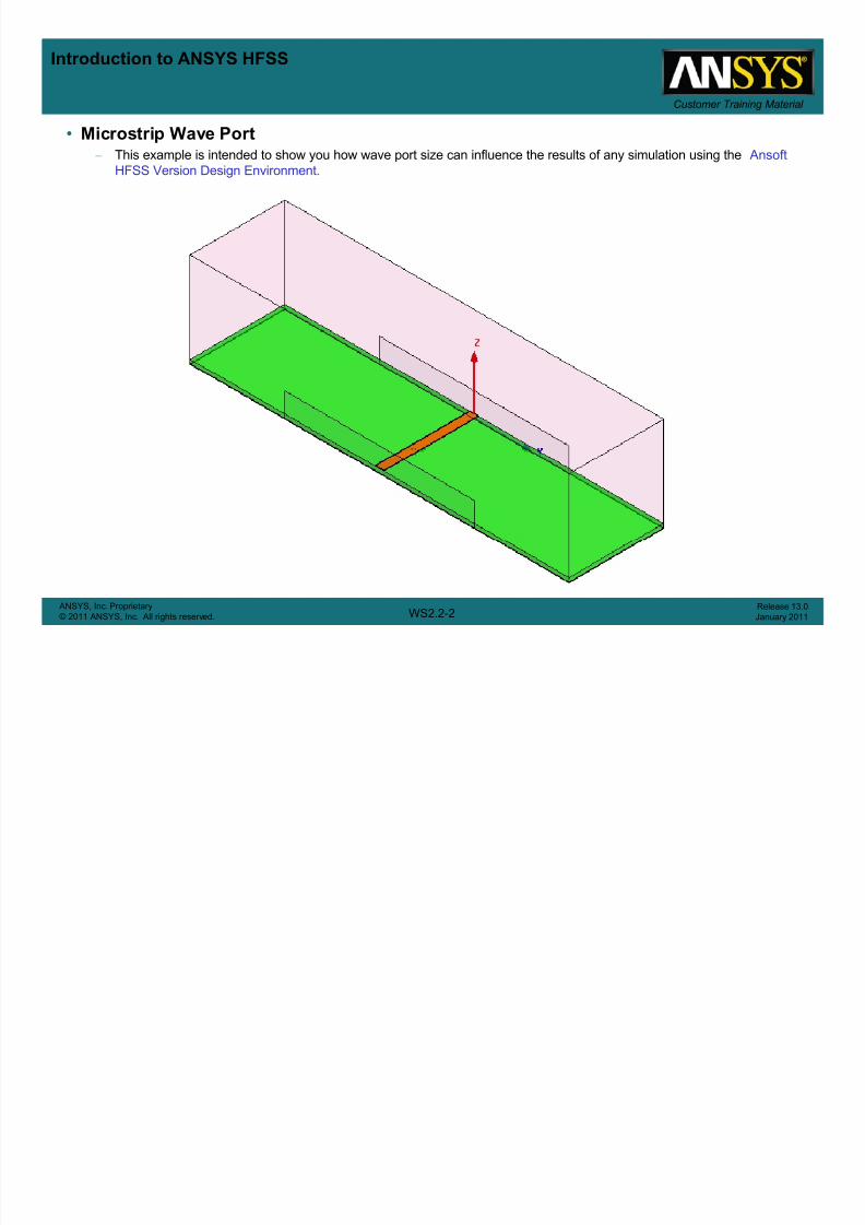
Microstrip Wave Port
ANSYS HFSS
WS2.2-1 ANSYS, Inc. Proprietary
© 2011 ANSYS, Inc. All rights reserved.Release 13.0
January 2011
7/26/2019 WS02 2 Hfss Microstrip Waveports
http://slidepdf.com/reader/full/ws02-2-hfss-microstrip-waveports 2/20
Introduction to ANSYS HFSS
Customer Training Material
• Microstrip Wave Port – This example is intended to show you how wave port size can influence the results of any simulation using the Ansoft
HFSS Version Design Environment.
WS2.2-2 ANSYS, Inc. Proprietary
© 2011 ANSYS, Inc. All rights reserved.Release 13.0
January 2011

7/26/2019 WS02 2 Hfss Microstrip Waveports
http://slidepdf.com/reader/full/ws02-2-hfss-microstrip-waveports 3/20
Introduction to ANSYS HFSS
Customer Training Material
• Design Review – Generally speaking when we assign a wave port to a microstrip line, or any quasi-TEM line, we need to include some
area around the actual transmission line. The big question is, “how much area?”
– Below you will see the cross section of a simple microstrip line with naming conventions shown.
~10w
~8h
– As a rule of thumb, we typically create a 2D rectangle to represent the wave port stimulus for this type of structure. The
h
substrate.
– REMEMBER: These are only guidelines !!!
– The height of the port will be affected by the permittivity of the substrate. The higher the
perm v y, e ess e e s w propaga e n e a r, an e s or er e por can e ma e. – The width of the port will affect the port impedance and propagating modes. The narrower the
width (image on right), the more the fields will couple to the side walls of the port. This effect may
not be physical. The wider the port, the greater chance that a higher frequency waveguide mode
can propagate.
WS2.2-3 ANSYS, Inc. Proprietary
© 2011 ANSYS, Inc. All rights reserved.Release 13.0
January 2011
– This example will explore this last phenomenon.

7/26/2019 WS02 2 Hfss Microstrip Waveports
http://slidepdf.com/reader/full/ws02-2-hfss-microstrip-waveports 4/20
Introduction to ANSYS HFSS
Customer Training Material Getting Started
• Launching Ansoft HFSS – To access Ansoft HFSS, click the Microsoft Start button, select All Programs, and select the Ansoft, HFSS 13.0
program group. Click HFSS 13.0.
• Setting Tool Options
– Note: In order to follow the steps outlined in this example, verify that the following tool options are set :
– Select the menu item Tools > Options > HFSS Options
• Click the General tab
– se zar s or a a npu w en crea ng new oun ar es: ec e
– Duplicate boundaries/mesh operations with geometry: Checked
• Click the OK button
– Select the menu item Tools > Options > Modeler Options.
• Click the O eration tab
– Automatically cover closed polylines: Checked
– Select last command on object select: Checked
• Click the Drawing tab
– Edit properties of new primitives: Checked
• c e u on
• Opening a New Project – In HFSS Desktop, click the On the Standard toolbar, or
WS2.2-4 ANSYS, Inc. Proprietary
© 2011 ANSYS, Inc. All rights reserved.Release 13.0
January 2011
.
– From the Project menu, select Insert HFSS Design.

7/26/2019 WS02 2 Hfss Microstrip Waveports
http://slidepdf.com/reader/full/ws02-2-hfss-microstrip-waveports 5/20
Introduction to ANSYS HFSS
Customer Training Material Creating the 3D Model
• Set Solution Type – Select the menu item HFSS > Solution Type
• Choose Driven Modal
• Click the OK button
• Set Model Units – Select the menu item Modeler > Units
• Select Units: mil
• Click the OK button
• Set Default Material – Using the 3D Modeler Materials toolbar, choose Select
• From the Select Definition window, click the Add Material button
• View/Edit Material Window:
– Material Name: My_Rogers
– Relative Permittivity: 3.38
–
• Click the OK button
WS2.2-5 ANSYS, Inc. Proprietary
© 2011 ANSYS, Inc. All rights reserved.Release 13.0
January 2011

7/26/2019 WS02 2 Hfss Microstrip Waveports
http://slidepdf.com/reader/full/ws02-2-hfss-microstrip-waveports 6/20
Introduction to ANSYS HFSS
Customer Training Material
• Create Substrate – Select the menu item Draw > Box
• Using the coordinate entry fields, enter the box position
– X: 0.0, Y: -400.0, Z: 0.0, Press the Enter key
• s ng t e coor nate entry e s, enter t e oppos te corner o t e ox:
–
dX: 200.0, dY: 800.0, dZ: 8.0, Press the Enter key – Select the Attribute tab from the Properties window.
• For the Value of Name type: Substrate
• Click the Edit button for the Value of Color to chan e the substrate color
• Click the OK button
– To fit the view:
• Select the menu item View > Fit All > Active View .
• Set Default Material – Using the 3D Modeler Materials toolbar, choose Select
• Type pec in the Search by Name field
• Click the OK button
WS2.2-6 ANSYS, Inc. Proprietary
© 2011 ANSYS, Inc. All rights reserved.Release 13.0
January 2011

7/26/2019 WS02 2 Hfss Microstrip Waveports
http://slidepdf.com/reader/full/ws02-2-hfss-microstrip-waveports 7/20
Introduction to ANSYS HFSS
Customer Training Material
• Create Trace – Select the menu item Draw > Box
• Using the coordinate entry fields, enter the box position
– X: 0.0, Y: -9.25, Z: 8.0, Press the Enter key
• s ng t e coor nate entry e s, enter t e oppos te corner o t e ox:
–
dX: 200.0, dY: 18.5, dZ: 1.4, Press the Enter key – Select the Attribute tab from the Properties window.
• For the Value of Name type: Trace
• Click the Edit button for the Value of Color to chan e the trace color
• Click the OK button
– To fit the view:
• Select the menu item View > Fit All > Active View .
• Create Ground – Select the menu item Draw > Box
• Using the coordinate entry fields, enter the box position
– X: 0.0, Y: -400.0, Z: 0.0, Press the Enter key
• s ng e coor na e en ry e s, en er e oppos e corner o e ox: – dX: 200.0, dY: 800.0, dZ: -1.4, Press the Enter key
– Select the Attribute tab from the Properties window.
• For the Value of Name type: Ground
• Click the Edit button for the Value of Color to chan e the round color
WS2.2-7 ANSYS, Inc. Proprietary
© 2011 ANSYS, Inc. All rights reserved.Release 13.0
January 2011
• Click the OK button

7/26/2019 WS02 2 Hfss Microstrip Waveports
http://slidepdf.com/reader/full/ws02-2-hfss-microstrip-waveports 8/20
Introduction to ANSYS HFSS
Customer Training Material
• Set Default Material – Using the 3D Modeler Materials toolbar, choose vacuum
• Create Air – Select the menu item Draw > Box
• Using the coordinate entry fields, enter the box position
– X: 0.0, Y: -400.0, Z: -1.4, Press the Enter key
• Using the coordinate entry fields, enter the opposite corner of the box:
– dX: 200.0, dY: 800.0, dZ: 200.0, Press the Enter key
– Select the Attribute tab from the Properties window.
• For the Value of Name type: Air
• Click the checkbox for the Value of the Display Wireframe attribute•
• Create Radiation Boundary – Select the menu item Edit > Select > By Name
• Select the ob ects named: Air
• Click the OK button
– Select the menu item HFSS > Boundaries > Assign > Radiation
• Name: Rad1
• Click the OK button
WS2.2-8 ANSYS, Inc. Proprietary
© 2011 ANSYS, Inc. All rights reserved.Release 13.0
January 2011

7/26/2019 WS02 2 Hfss Microstrip Waveports
http://slidepdf.com/reader/full/ws02-2-hfss-microstrip-waveports 9/20
Introduction to ANSYS HFSS
Customer Training Material
• Set Grid Plane – Select the menu item Modeler > Grid Plane > YZ
• Create the Wave Port – Select the menu item Draw > Rectangle
• Using the coordinate entry fields, enter the center position
– X: 0.0, Y: -200.0, Z: 0.0, Press the Enter key
• Using the coordinate entry fields, enter the opposite corner of the rectangle:
– dX: 0.0, dY: 400.0, dZ: 50.0, Press the Enter key
– Select the Attribute tab from the Properties window.
• For the Value of Name type: Port1
• Click the OK button – -
• For Position, type: 0mil, -Port_Width/2, 0mil, Click the Tab key to accept
– Add Variable dialog
• Unit Type: Length
• Unit: mil
• Value: 400 – Click the OK button
• For YSize, type: Port_Width, Click the Tab key to accept
• Click OK to accept changes to the port object
WS2.2-9 ANSYS, Inc. Proprietary
© 2011 ANSYS, Inc. All rights reserved.Release 13.0
January 2011

7/26/2019 WS02 2 Hfss Microstrip Waveports
http://slidepdf.com/reader/full/ws02-2-hfss-microstrip-waveports 10/20
Introduction to ANSYS HFSS
Customer Training Material
• Assign the Excitation 1 – Select the menu item Edit > Select > By Name
• Select the objects named: Port1
• Click the OK button
– e ect t e menu tem > xc tat ons > ss gn > ave ort
• Wave Port : General – Name: 1,
– Click the Next button
• Wave Port : Modes
– Number of Modes: 5
– For Mode 1, click the None in the Integration Line column
and select New Line
– Using the coordinate entry fields, enter the vector position
• X: 0.0, Y: 0.0, Z: 0.0, Press the Enter key
– Using the coordinate entry fields, enter the vertex
• dX: 0.0, dY: 0.0, dZ: 8.0, Press the Enter key
– For Mode 1, click the Zpi entry in the Characteristic Impedance
– Click the Next button
• Wave Port : Post Processing
– Click the Finish button
WS2.2-10 ANSYS, Inc. Proprietary
© 2011 ANSYS, Inc. All rights reserved.Release 13.0
January 2011

7/26/2019 WS02 2 Hfss Microstrip Waveports
http://slidepdf.com/reader/full/ws02-2-hfss-microstrip-waveports 11/20
Introduction to ANSYS HFSS
Customer Training Material
• Create Wave Port Excitation 2 – Select the menu item Edit > Select > By Name
• Select the objects named: Port1
• Click the OK button
– e ect t e menu tem, t > up cate > ong ne
• Using the coordinate entry fields, enter the first point of the duplicate vector – X: 0.0, Y: 0.0, Z: 0.0, Press the Enter key
• Using the coordinate entry fields, enter the second point of the duplicate vector
– dX: 200.0 dY: 0.0 dZ: 0.0 Press the Enter ke
• Duplicate Along Line window
– Total Number: 2
– Click the OK button
• Click the OK button
WS2.2-11 ANSYS, Inc. Proprietary
© 2011 ANSYS, Inc. All rights reserved.Release 13.0
January 2011

7/26/2019 WS02 2 Hfss Microstrip Waveports
http://slidepdf.com/reader/full/ws02-2-hfss-microstrip-waveports 12/20
Introduction to ANSYS HFSS
Customer Training Material
• Boundary Display – Select the menu item HFSS > Boundary Display (Solver View)
• From the Solver View of Boundaries, toggle the Visibility check box for the boundaries you wish to display.
– Note: The background (Perfect Conductor) is displayed as the outer boundary.
– ote: e er ect on uctors are sp aye as t e smeta oun ary.
–
Note: Select the menu item, View > Visibility to hide all of the geometry objects. This makes it easier tosee the boundary
• Click the Close button when you are finished
WS2.2-12 ANSYS, Inc. Proprietary
© 2011 ANSYS, Inc. All rights reserved.Release 13.0
January 2011

7/26/2019 WS02 2 Hfss Microstrip Waveports
http://slidepdf.com/reader/full/ws02-2-hfss-microstrip-waveports 13/20
Introduction to ANSYS HFSS
Customer Training Material
• Creating an Analysis Setup – Select the menu item HFSS > Analysis Setup > Add Solution Setup
• Click the General tab:
– Solution Frequency: 20GHz
• ec o ve orts n y
• Click the OK button
• Adding a Frequency Sweep – Select the menu item HFSS > Analysis Setup > Add Frequency Sweep
• Select Solution Setup: Setup1
• Click the OK button
– Edit Sweep Window:
• Frequency Setup Type: Linear Count
– Start: 0.1GHz
– Stop: 50.1GHz
– Count: 81
• Interpolating Sweep Options – Max. Solutions: 50
– Error Tolerance: 0.5%
• Click the OK button
WS2.2-13 ANSYS, Inc. Proprietary
© 2011 ANSYS, Inc. All rights reserved.Release 13.0
January 2011

7/26/2019 WS02 2 Hfss Microstrip Waveports
http://slidepdf.com/reader/full/ws02-2-hfss-microstrip-waveports 14/20
Introduction to ANSYS HFSS
Customer Training Material Analysis
• Save Project – Select the menu item File > Save As.
• From the Save As window, type the Filename: hfss_waveports
• Click the Save button
• Model Validation – Select the menu item HFSS > Validation Check
– Click the Close button (Note: To view any errors or warning messages, use the Message Manager.)
• Analyze – Select the menu item HFSS > Analyze All
• Simulation Warnings – Upon completion of the simulation you will get the following message:
– This warning is acceptable for this exercise, however, in general, if you receive this warning, you should increase the
Max. Solutions in the Interpolating Sweep options or increase the Error Tolerance. This warning could indicate a loss in
accuracy of the S-parameters for the Interpolating sweep.
WS2.2-14 ANSYS, Inc. Proprietary
© 2011 ANSYS, Inc. All rights reserved.Release 13.0
January 2011

7/26/2019 WS02 2 Hfss Microstrip Waveports
http://slidepdf.com/reader/full/ws02-2-hfss-microstrip-waveports 15/20
Introduction to ANSYS HFSS
Customer Training Material
• Solution Data – Select the menu item HFSS > Results > Solution Data
– To view the Profile, Click the Profile Tab.
– To view the Convergence, Click the Convergence Tab
• ote: e e au t v ew s or convergence s a e. e ect t e ot
radio button to view a graphical representations of the convergence
data.
– To view the Matrix Data, Click the Matrix Data Tab
• Note: To view a real-time update of the Matrix Data,
set the Simulation to Setup1, Last Adaptive
– To view the Mesh Statistics, Click the Mesh Statistics Tab.
• Click the Close button
• Create Propagation Constant vs. Frequency – Select the menu item HFSS > Results > Create Modal Solution
Data Report > Rectangular Plot
• Solution: Setup1: Sweep1
• oma n: weep
• Category: Gamma
• Quantity: Gamma(p1:1),Gamma(p1:2), Gamma(p1:3), Gamma(p1:4), Gamma(p1:5)
• Function: im
• Click the New Re ort button
WS2.2-15 ANSYS, Inc. Proprietary
© 2011 ANSYS, Inc. All rights reserved.Release 13.0
January 2011
• Click the Close button
• See next page for plot and discussion of results

7/26/2019 WS02 2 Hfss Microstrip Waveports
http://slidepdf.com/reader/full/ws02-2-hfss-microstrip-waveports 16/20
Introduction to ANSYS HFSS
Customer Training Material
• Discussion – What does this plot tell us?
• Given the physical size of the wave port object that we created, the fundamental mode (p2:1) is a quasi-TEM
mode that propagates from DC on up.
• .
starts propagating at ~14 GHz.
• Therefore, if we only needed to simulate up to 10 GHz, we wouldn’t need to size our port any different, however, if
we need to simulate up to 50 GHz, then we need to resize our port to eliminate the higher order propagating
modes.
• e as par o e exerc se w exp ore s.
WS2.2-16 ANSYS, Inc. Proprietary
© 2011 ANSYS, Inc. All rights reserved.Release 13.0
January 2011
7/26/2019 WS02 2 Hfss Microstrip Waveports
http://slidepdf.com/reader/full/ws02-2-hfss-microstrip-waveports 17/20
Introduction to ANSYS HFSS
Customer Training Material
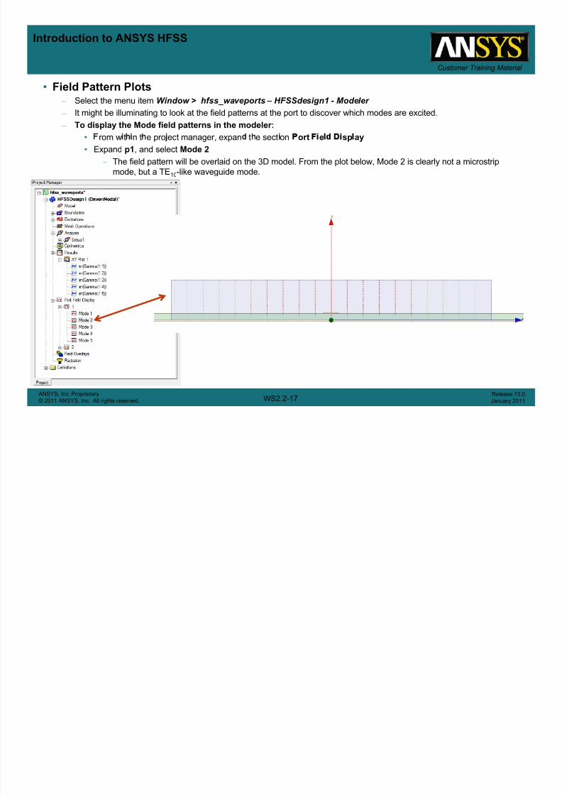
• Field Pattern Plots – Select the menu item Window > hfss_waveports – HFSSdesign1 - Modeler
– It might be illuminating to look at the field patterns at the port to discover which modes are excited.
– To display the Mode field patterns in the modeler:
• rom w t n t e pro ect manager, expan t e sect on ort e sp ay
• Expand p1, and select Mode 2
– The field pattern will be overlaid on the 3D model. From the plot below, Mode 2 is clearly not a microstrip
mode, but a TE10-like waveguide mode.
WS2.2-17 ANSYS, Inc. Proprietary
© 2011 ANSYS, Inc. All rights reserved.Release 13.0
January 2011

7/26/2019 WS02 2 Hfss Microstrip Waveports
http://slidepdf.com/reader/full/ws02-2-hfss-microstrip-waveports 18/20
Introduction to ANSYS HFSS
Customer Training Material Optimetrics
• Add a Parametric Sweep – Select the menu item HFSS > Optimetrics Analysis > Add Parametric
• Click the Sweep Definitions tab:
– Click the Add button
– t weep a og
• Variable: Port_Width
• Select Linear Step
• Start: 200mil
• Sto : 600mil
• Step: 100mil
• Click the Add >> button
• Click the OK button
• Click the OK button
• Save Project – Select the menu item File > Save.
• Analyze – Expand the Project Tree to display the items listed under Optimetrics
– Right-click the mouse on ParametricSetup1 and choose Analyze
WS2.2-18 ANSYS, Inc. Proprietary
© 2011 ANSYS, Inc. All rights reserved.Release 13.0
January 2011

7/26/2019 WS02 2 Hfss Microstrip Waveports
http://slidepdf.com/reader/full/ws02-2-hfss-microstrip-waveports 19/20
Introduction to ANSYS HFSS
Customer Training Material
• Create Propagation Constant vs. Frequency vs. Port_Width – Select the menu item HFSS > Results > Create Modal Solution Data Report > Rectangular Plot
• Solution: Setup1: Sweep1
• Domain: Sweep
• ategory: amma
• Quantity: Gamma(p1:2),
• Function: im
• Click the New Report button
• Click the Close button
• Discussion –
– This shows that as we decrease the width of the port, the frequency at which the higher order mode starts to
propagate increases.
– Therefore, by properly sizing the wave port, you can eliminate any higher order propagating modes if you believe
that they do not exist.
WS2.2-19 ANSYS, Inc. Proprietary
© 2011 ANSYS, Inc. All rights reserved.Release 13.0
January 2011
– You need to use caution if you are simulating very high frequencies, i.e., millimeter wavelengths, as you may not
be able to make the ports small enough to eliminate these modes. You probably shouldn’t even try as the higher
order modes might represent real world effects.

7/26/2019 WS02 2 Hfss Microstrip Waveports
http://slidepdf.com/reader/full/ws02-2-hfss-microstrip-waveports 20/20
Introduction to ANSYS HFSS
Customer Training Material
• Create Propagation Constant vs. Port Width at a fixed frequency – Select the menu item HFSS > Results > Create Modal Solution Data Report > Rectangular Plot
• Solution: Setup1: PortOnly
• Domain: Sweep
• : ort t
• Category: Gamma
• Quantity: Gamma(p1:2),
• Function: im
• Click the New Re ort button
• Click the Close button
WS2.2-20 ANSYS, Inc. Proprietary
© 2011 ANSYS, Inc. All rights reserved.Release 13.0
January 2011