würth elektronik circuit board technology · summary seite 42 05.12.2017 dient-leistungen...
TRANSCRIPT
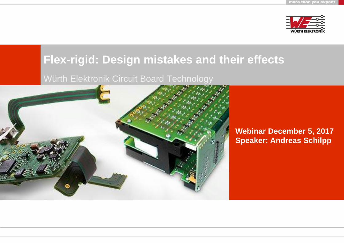
Flex-rigid: Design mistakes and their effects
Würth Elektronik Circuit Board Technology
Webinar December 5, 2017
Speaker: Andreas Schilpp

Agenda
Introduction Flex-Rigid
Design Standards, Design Rules
Examples, Consequences, Tips
Combination of Technologies
Summary, Q&A
www.we-online.de Seite 2 05.12.2017
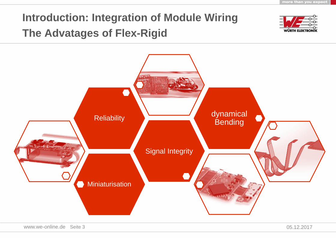
Introduction: Integration of Module Wiring
The Advatages of Flex-Rigid
Miniaturisation
Signal Integrity
ReliabilitydynamicalBending
05.12.2017Seite 3www.we-online.de
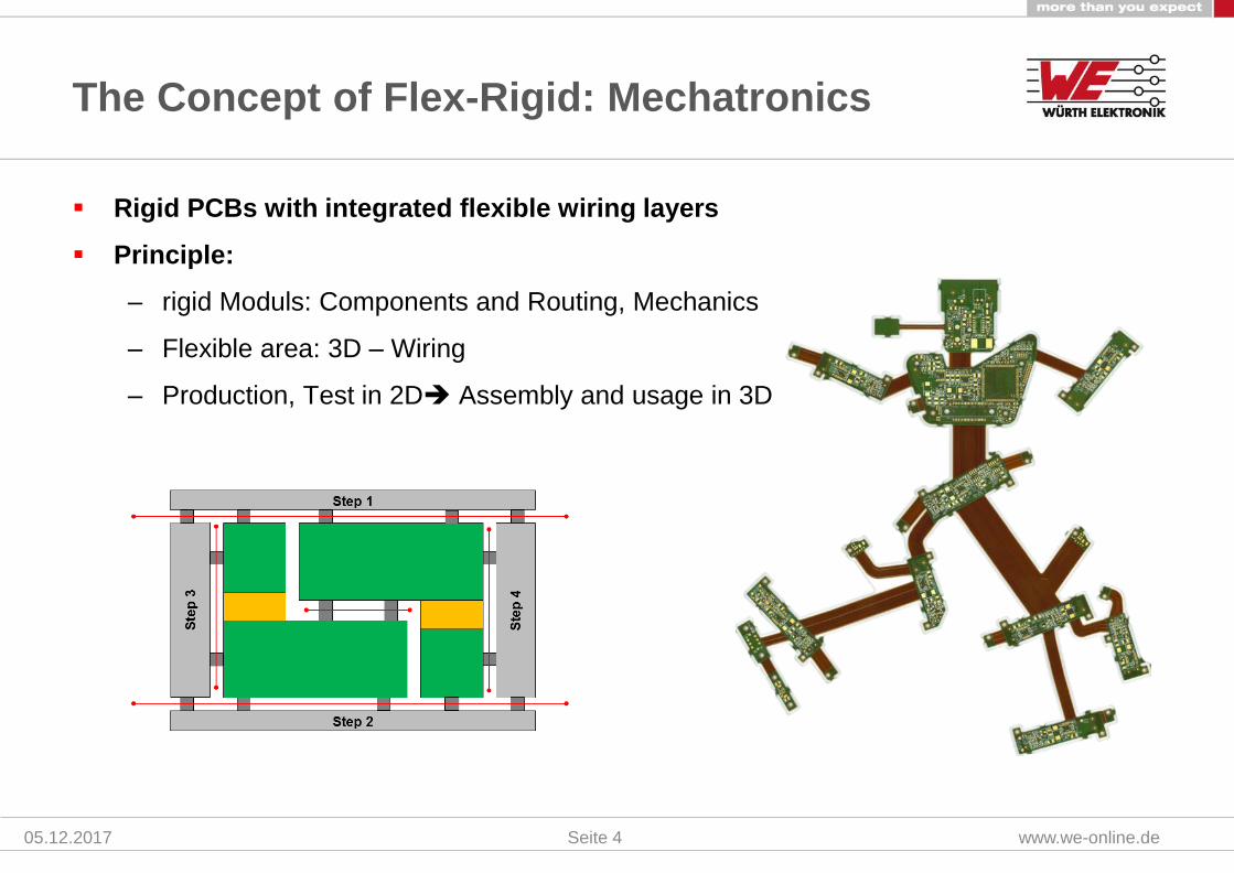
The Concept of Flex-Rigid: Mechatronics
Rigid PCBs with integrated flexible wiring layers
Principle:
– rigid Moduls: Components and Routing, Mechanics
– Flexible area: 3D – Wiring
– Production, Test in 2D Assembly and usage in 3D
05.12.2017 Seite 4 www.we-online.de
Agenda
Introduction Flex-Rigid
Design Standards, Design Rules
Examples, Consequences, Tips
Combination of Technologies
Summary, Q&A
www.we-online.de Seite 5 05.12.2017
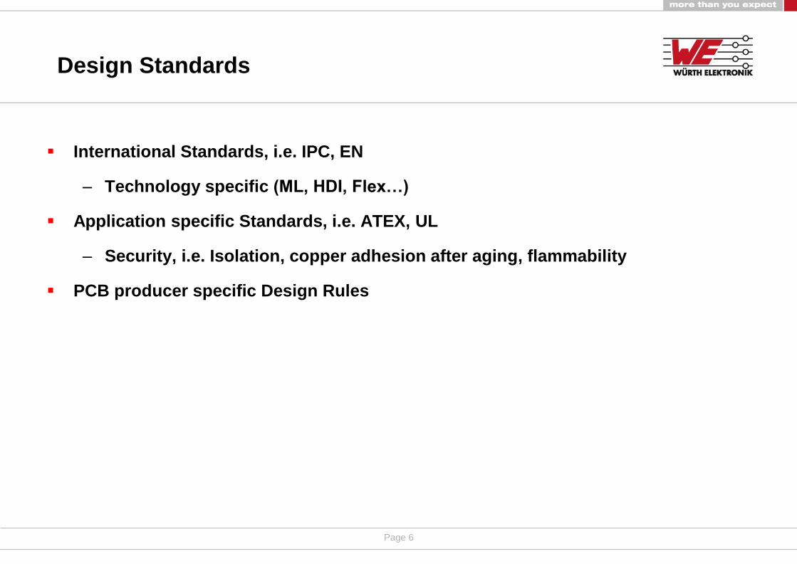
Design Standards
International Standards, i.e. IPC, EN
– Technology specific (ML, HDI, Flex…)
Application specific Standards, i.e. ATEX, UL
– Security, i.e. Isolation, copper adhesion after aging, flammability
PCB producer specific Design Rules
Page 6

IPC Standards
Acceptability of Printed Boards: IPC-A-600
Material
Design: IPC-2223
Qualification and Performance Spec: IPC-6013
……
Page 7

IPC-A-600H
www.we-online.de Seite 8 05.12.2017
Description Transition Zone: +/- 1,5mm

IPC-6013C - Definition
www.we-online.de Seite 9 05.12.2017
Grey Area
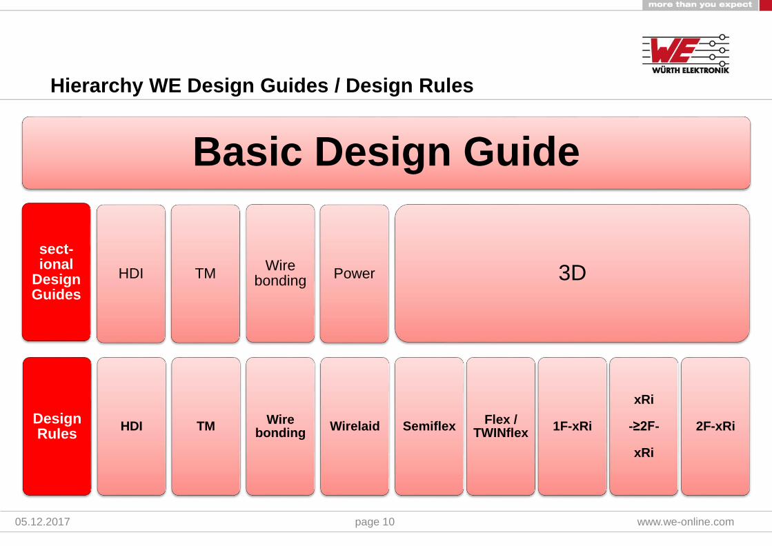
Hierarchy WE Design Guides / Design Rules
Basic Design Guide
sect-ional
Design Guides
Design Rules
HDI
HDI
TM
TM
Wirebonding
Wirebonding
Power
Wirelaid
3D
SemiflexFlex /
TWINflex1F-xRi
xRi
-≥2F-
xRi
2F-xRi
05.12.2017 page 10 www.we-online.com
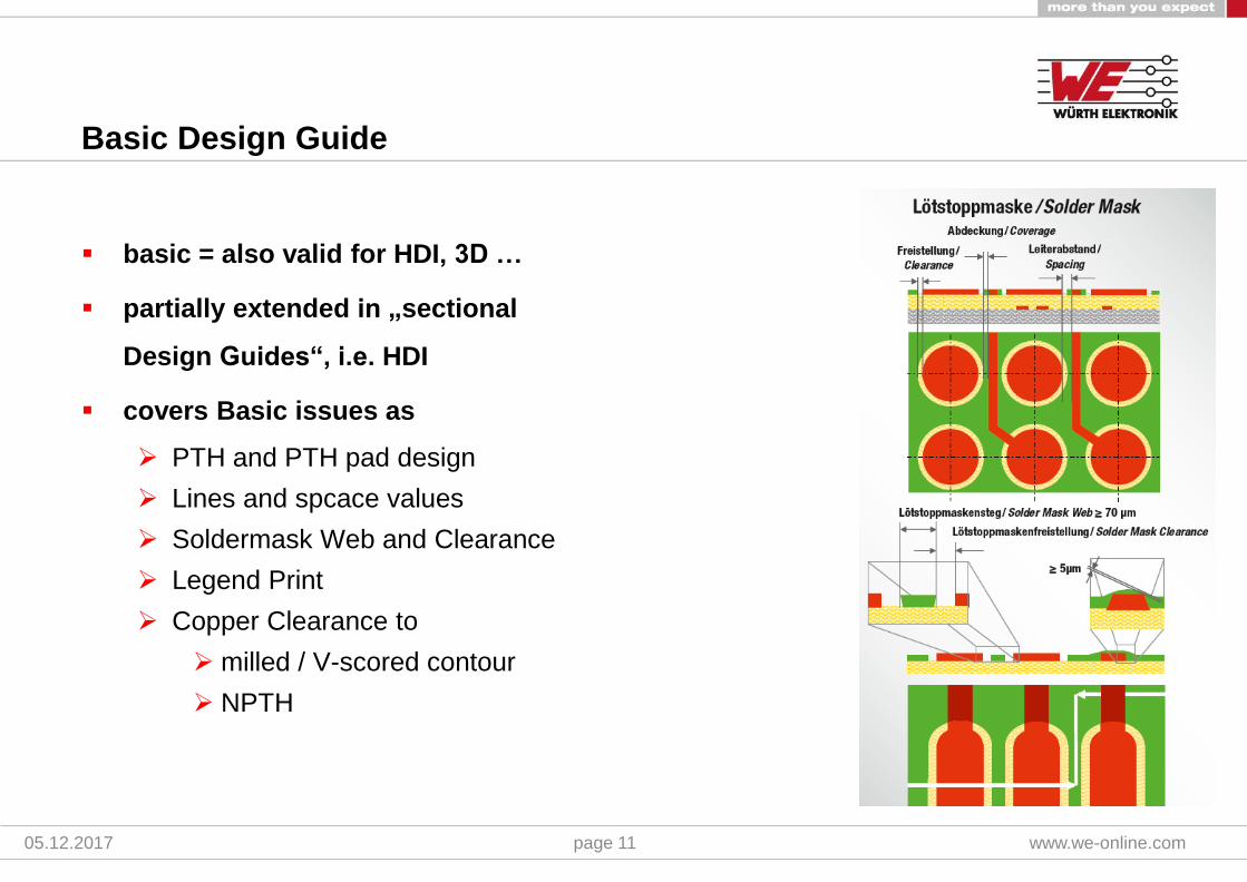
Basic Design Guide
basic = also valid for HDI, 3D …
partially extended in „sectional
Design Guides“, i.e. HDI
covers Basic issues as
PTH and PTH pad design
Lines and spcace values
Soldermask Web and Clearance
Legend Print
Copper Clearance to
milled / V-scored contour
NPTH
05.12.2017 page 11 www.we-online.com

Sense of Annular Rings
Layout / Screen:
Real life
IPC-A-600H:
05.12.2017Seite 12www.we-online.de

Most common Mistake: Standard Rules Item „G“ not regarded
– Spacing Vias to Flex-Rigid Transition
Distance to the Via Pad!
IPC-2223:
05.12.2017 page 13 www.we-online.com
Design Rules Flex-Rigid – Spacing Vias / Pads
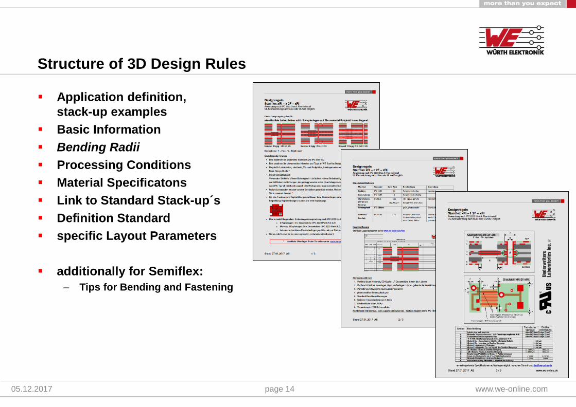
Application definition,
stack-up examples
Basic Information
Bending Radii
Processing Conditions
Material Specificatons
Link to Standard Stack-up´s
Definition Standard
specific Layout Parameters
additionally for Semiflex:
– Tips for Bending and Fastening
Structure of 3D Design Rules
05.12.2017 page 14 www.we-online.com

05.12.2017
Mechanical Design influences expense for PCB production: Array Creation
– reduces expense
– improves Registration Accuracy
www.we-online.de Seite 15
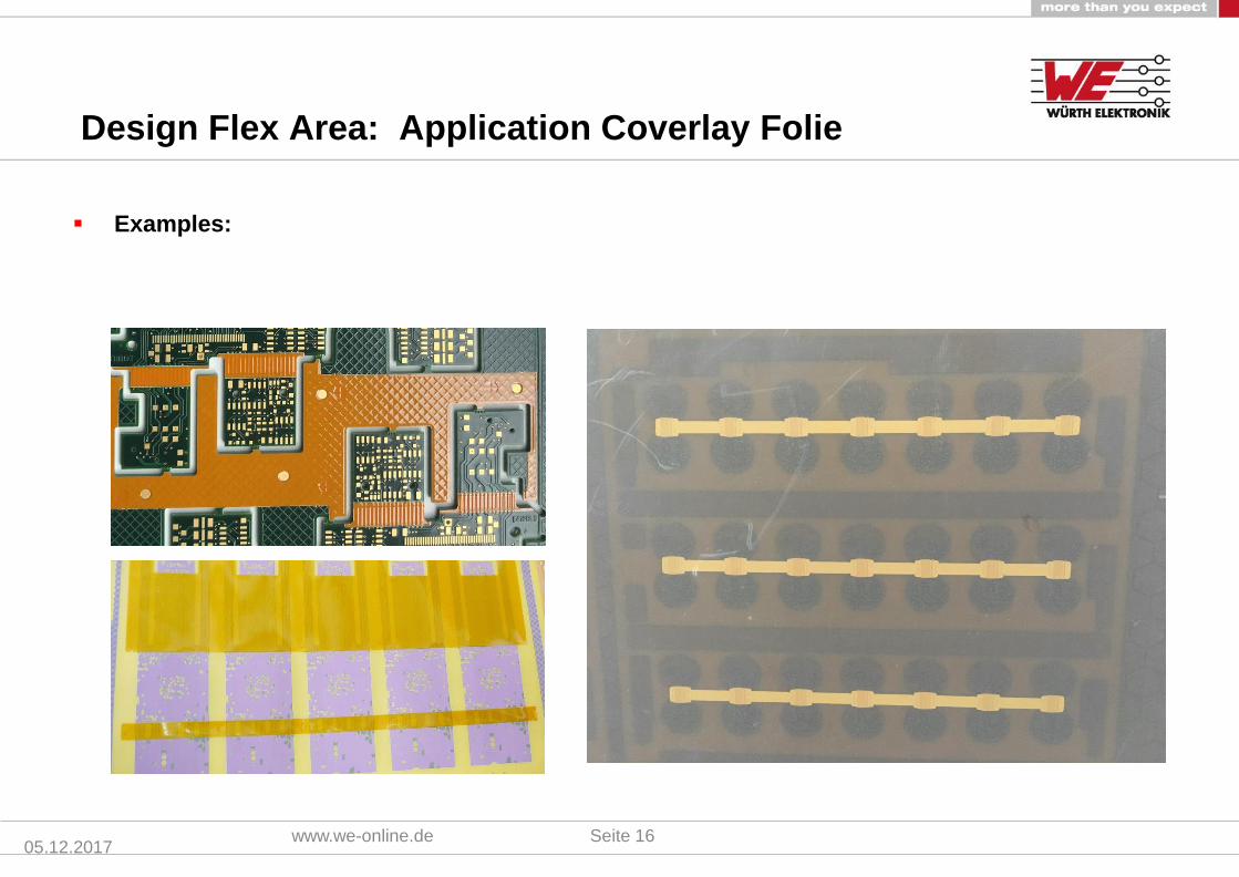
Design Flex Area: Application Coverlay Folie
RIGID FLEX RIGID RIGID FLEX RIGIDFLEX
RIGID FLEX RIGID
>4mm
05.12.2017
Examples:
www.we-online.de Seite 16
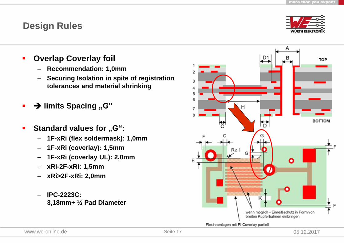
Design Flex Area: Application Coverlay Folie
Design Rules
www.we-online.de Seite 17 05.12.2017
Overlap Coverlay foil
– Recommendation: 1,0mm
– Securing Isolation in spite of registration
tolerances and material shrinking
limits Spacing „G"
Standard values for „G“:
– 1F-xRi (flex soldermask): 1,0mm
– 1F-xRi (coverlay): 1,5mm
– 1F-xRi (coverlay UL): 2,0mm
– xRi-2F-xRi: 1,5mm
– xRi>2F-xRi: 2,0mm
– IPC-2223C:
3,18mm+ ½ Pad Diameter
Agenda
Introduction Flex-Rigid
Design Standards, Design Rules
Examples, Consequences, Tips
Combination of Technologies
Summary, Q&A
www.we-online.de Seite 18 05.12.2017
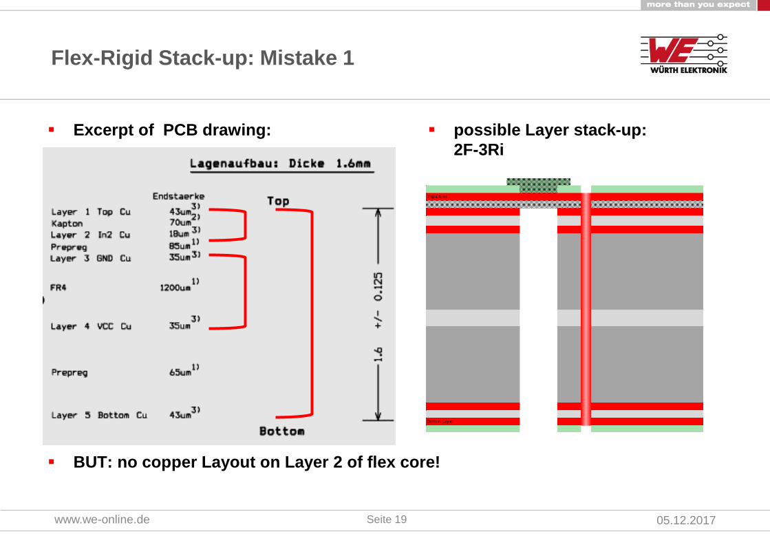
Flex-Rigid Stack-up: Mistake 1
www.we-online.de Seite 19 05.12.2017
Excerpt of PCB drawing:
BUT: no copper Layout on Layer 2 of flex core!
possible Layer stack-up:
2F-3Ri

www.we-online.de Seite 20 05.12.2017
much better Stack-up:
1F-4Ri
Cost Savings: about 30% with same Performance!
at the same time reduced Risk of Warpage!
possible Layer stack-up :
2F-3Ri
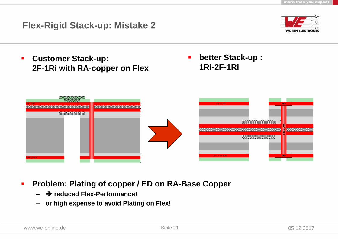
Flex-Rigid Stack-up: Mistake 1
www.we-online.de Seite 21 05.12.2017
Customer Stack-up:
2F-1Ri with RA-copper on Flex
Problem: Plating of copper / ED on RA-Base Copper
– reduced Flex-Performance!
– or high expense to avoid Plating on Flex!
better Stack-up :
1Ri-2F-1Ri
Flex-Rigid Stack-up: Mistake 2
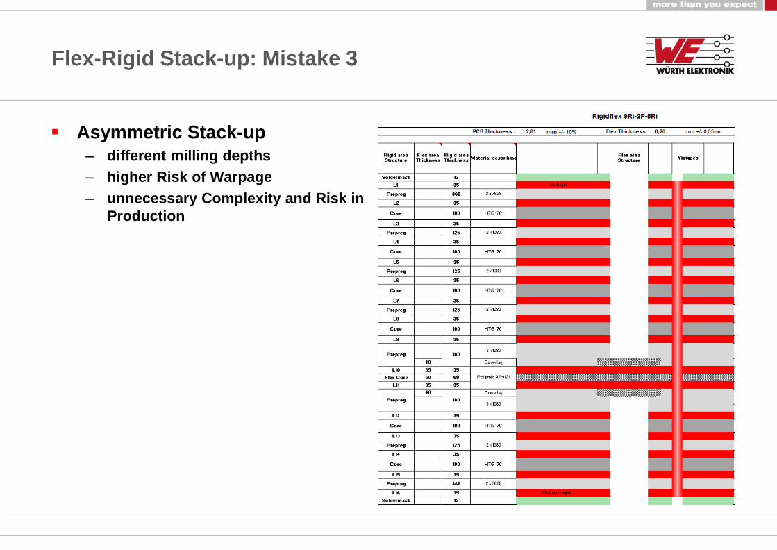
Asymmetric Stack-up
– different milling depths
– higher Risk of Warpage
– unnecessary Complexity and Risk in
Production
Flex-Rigid Stack-up: Mistake 3
05.12.2017page 23www.we-online.de
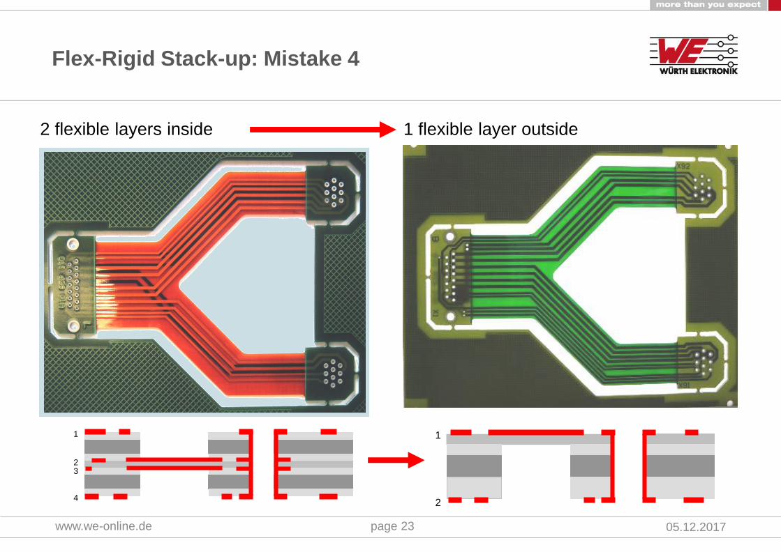
2 flexible layers inside 1 flexible layer outside
1
2
1
23
4
Flex-Rigid Stack-up: Mistake 4
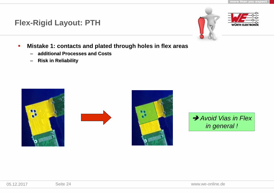
Mistake 1: contacts and plated through holes in flex areas
– additional Processes and Costs
– Risk in Reliability
Flex-Rigid Layout: PTH
05.12.2017 Seite 24 www.we-online.de
Avoid Vias in Flex
in general !

Mistake 2 : NFP Removal
– Drilling quality in flexible core could become
dramatically worse!
– Consequence: Plating problems and thus
problems in Reliability
Don´t perform NFP Removal
on Flex Layers! „R“
Mistake 3: AR Aspect Ratio too large
(PCB Thickness T / PTH-Diameter B)
– reduced copper distribution in barrel
– reduced barrel stability, current capacity and heat transfer
– Risk of barrel cracking in case of thermal load
– for Flex-Rigid with Flex core inside even more problematic
Flex-Rigid Layout: PTH
05.12.2017 Seite 25 www.we-online.de
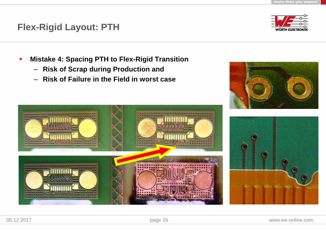
Mistake 4: Spacing PTH to Flex-Rigid Transition
– Risk of Scrap during Production and
– Risk of Failure in the Field in worst case
05.12.2017 page 26 www.we-online.com
Flex-Rigid Layout: PTH
05.12.2017 page 27 www.we-online.com
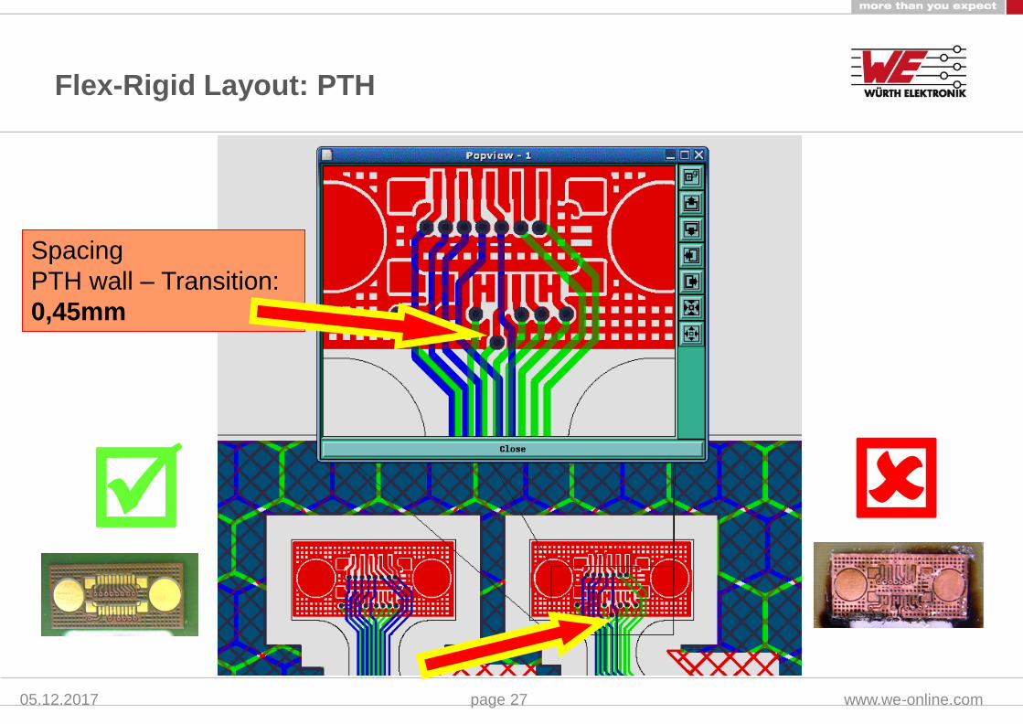
Spacing
PTH wall – Transition:
0,45mm
Flex-Rigid Layout: PTH
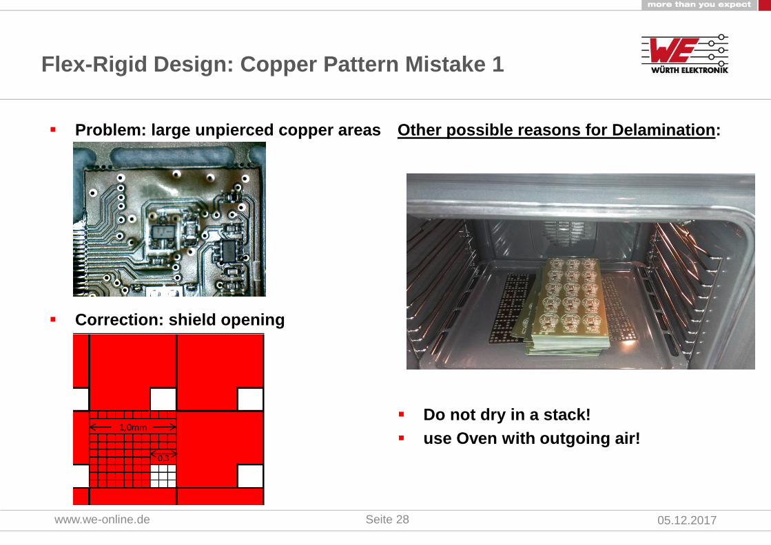
Problem: large unpierced copper areas
Correction: shield opening
Other possible reasons for Delamination:
Do not dry in a stack!
use Oven with outgoing air!
05.12.2017Seite 28www.we-online.de
Flex-Rigid Design: Copper Pattern Mistake 1

Mistake 2 : copper lines on same place on all flexible layers
– partially big differences in Thickness
– bad pressure distribution during Lamination process
– Reduction in Flexibility resp. Bendability
Solution: Copper Offset
05.12.2017Seite 29www.we-online.de
Flex-Rigid Design: Copper Pattern

Airgap-Stack-up– Flex Length „H“ too small
– „Buckling“ makes flexible area very
stiff
Recommendation:
– H ≥ 50mm
05.12.2017Seite 30www.we-online.de
Flex-Rigid Mechanics: Mistake 1
05.12.2017Seite 31www.we-online.de
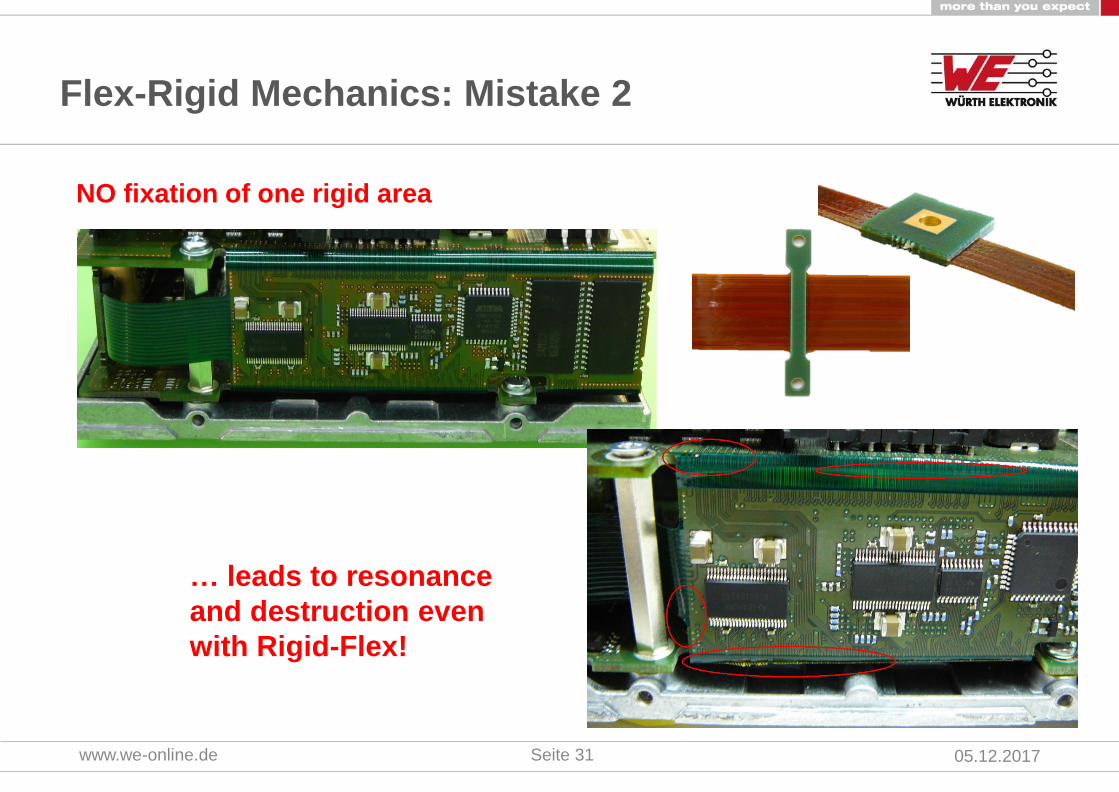
NO fixation of one rigid area
… leads to resonance
and destruction even
with Rigid-Flex!
Flex-Rigid Mechanics: Mistake 2
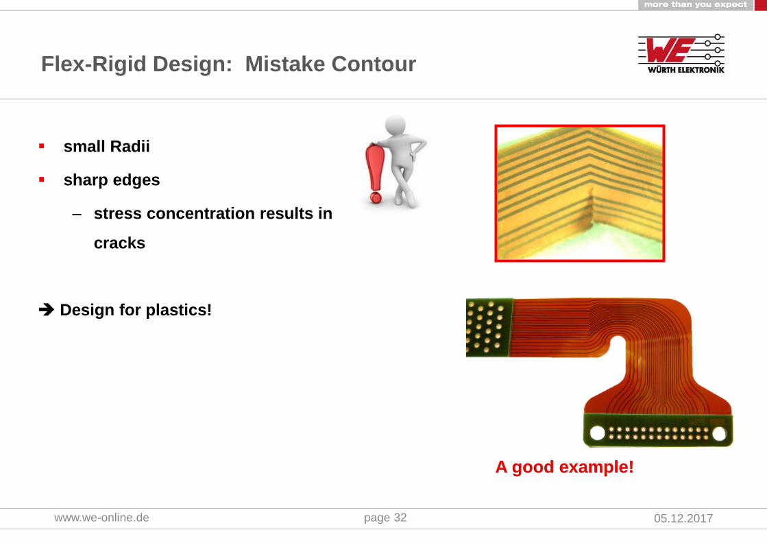
05.12.2017page 32www.we-online.de
A good example!
small Radii
sharp edges
– stress concentration results in
cracks
Design for plastics!
Flex-Rigid Design: Mistake Contour

05.12.2017 Seite 33 www.we-online.de
Array too solide, hard to separate
Missing of break points
circulating stable frame
– Damaging of flexible Area during Separation
Flex-Rigid Design: Mistake Delivery Array
05.12.2017 Seite 34 www.we-online.de
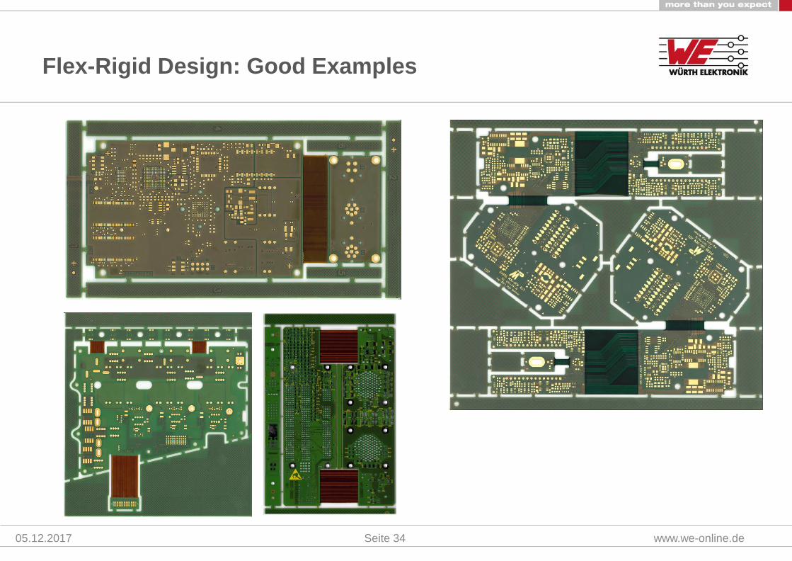
Flex-Rigid Design: Good Examples

www.we-online.de Seite 35 05.12.2017
Flex-Rigid Design: Good Examples
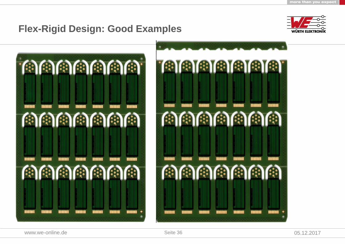
www.we-online.de Seite 36 05.12.2017
Flex-Rigid Design: Good Examples
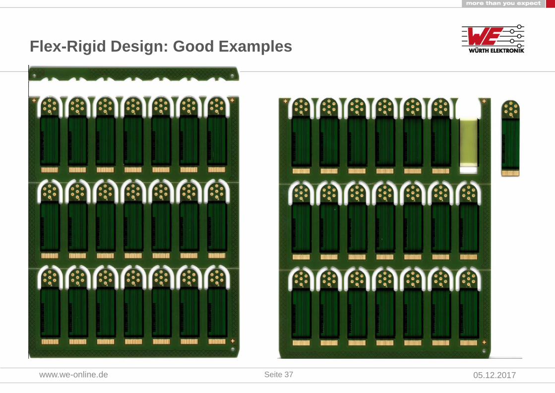
www.we-online.de Seite 37 05.12.2017
Flex-Rigid Design: Good Examples

www.we-online.de Seite 38 05.12.2017
Flex-Rigid Design: Good Examples

Agenda
Introduction Flex-Rigid
Design Standards, Design Rules
Examples, Consequences, Tips
Combination of Technologies
Summary, Q&A
www.we-online.de Seite 39 05.12.2017
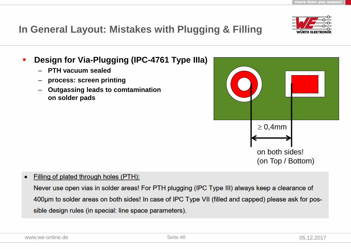
www.we-online.de Seite 40 05.12.2017
Design for Via-Plugging (IPC-4761 Type IIIa)
– PTH vacuum sealed
– process: screen printing
– Outgassing leads to comtamination
on solder pads
0,4mm
on both sides!
(on Top / Bottom)
In General Layout: Mistakes with Plugging & Filling

www.we-online.de Seite 41 05.12.2017
Design for Via-Filling (IPC-4761 Type VII)
– multiple Plating processes increase copper thickness
– thicker copper = larger design structures (spacing)
Limitation of design structures as a consequence
of Combination of Technologies und Processes
– Microvia copper filling
– PTH filled & capped
– AND open PTH !!!!
Smallest Structures dependant on combination:
– 100µm / 125µm / 150µm
in any case please check with your supplier
IPC 4761 Type VII „Filling capped“ Via mit Harz gefüllt und Überkupfert!
Einsatzfeld:
- Kühlkörperflächen
- Vias in Lötflächen
- Vakuumdichtigkeit
In General Layout: Mistakes with Plugging & Filling
Summary
www.we-online.de Seite 42 05.12.2017
Dient-leistungen
Knowledge of Design Rules
– helps avoiding Mistakes and Costs
– saves valuable time by avoiding technical queries
– saves reliable Function of the Application
Our Design Rules are revised regularly
– please don´t use old copies
– newest Revision always in Internet
In case of questions or suggestions:
Please contact us!
Emails are welcome via our Team-Address:
Thank you very much for your attention!
05.12.2017Seite 43www.we-online.de