written exam with solutions ie1204-5 digital design friday
TRANSCRIPT

1
Written exam with solutions IE1204-5 Digital Design
Friday 21/10 2016 09.00-13.00
General Information Examiner: Ingo Sander.
Teacher: Kista, William Sandqvist tel 08-7904487, Elena Dubrova phone 08-790 41 14 Exam text does not have to be returned when you hand in your writing. Aids: No aids are allowed! The exam consists of three parts with a total of 14 tasks, and a total of 30 points:
Part A1 (Analysis) containes ten short questions. Right answer will give you one point. Incorrect answer will give you zero points. The total number of points in Part A1 is 10 points. To pass the Part A1 requires at least 6p, if you get fewer points, we will not look at the rest of your exam.
Part A2 (Methods) contains two methodology-related problems with a total of 10 points.
To pass the exam requires at least 11 points from A1 + A2 , if you get fewer points, we will not look at the rest of your exam.
Part B (Design problems) contains two design problems with total of 10 points. Part B is
corrected only if there are at least 11p from the exam A- Part.
NOTE ! At the end of the exam text there is a submission sheet for Part A1, which should be
separated and submitted together with the solutions for A2 and B.
A passing grade (E ) requires at least 11 points on the exam. If you get exactly 10p from A1(6p)+A2(4p), (FX), completion to (E) will be offered.
Grades are given as follows:
0 – 11 – 16 – 19 – 22 – 25 F E D C B A
The result is expected to be announced before Friday 11/11 2016.

2
Part A1: Analysis Only final answers are required in Part A1. Write these answers on the submission sheet for Part A1, which can be found at the end of the exam text. 1. 1p/0p
A function f(x, y, z) is described by the expression:
)()(),,( xyxyxzxzzyxf +⋅⊕+⊕=
Write down a minimized two-level sum-of-products (SoP) form for this function..
{ } ?),,( min == SoPzyxf
1. Proposed solution.
yyxzyxzyxzyzx
xxyxzxzxyxyxzxzzyxf
=+++=
=+⋅⊕+⊕=+⋅⊕+⊕= )()()()(),,(
2. 1p/0p A four-bit unsigned integer x = (x3x2x1x0) is connected to a 6-bit adder in the way that it is multiplied with a constant K, so that the result is s = K⋅x (see the diagram below to figure out the value of K). If the input x = (1111)2 is applied to the diagram below, then what will the number s = ? Answer with s as a binary number.
2. Proposed solution. s = 1∙x+4∙x = 5∙x 5∙15 = 75 10010112
3
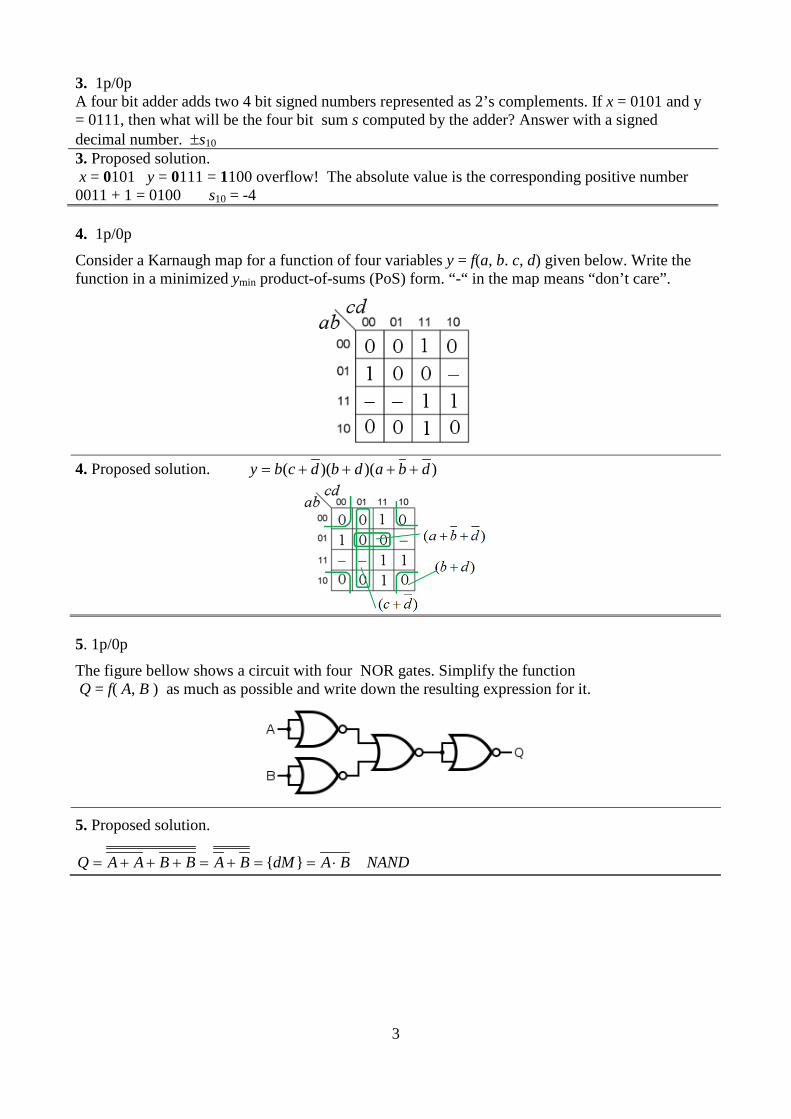
3. 1p/0p A four bit adder adds two 4 bit signed numbers represented as 2’s complements. If x = 0101 and y = 0111, then what will be the four bit sum s computed by the adder? Answer with a signed decimal number. ±s10 3. Proposed solution. x = 0101 y = 0111 = 1100 overflow! The absolute value is the corresponding positive number 0011 + 1 = 0100 s10 = -4 4. 1p/0p
Consider a Karnaugh map for a function of four variables y = f(a, b. c, d) given below. Write the function in a minimized ymin product-of-sums (PoS) form. “-“ in the map means “don’t care”.
4. Proposed solution. ))()(( dbadbdcby ++++=
5. 1p/0p
The figure bellow shows a circuit with four NOR gates. Simplify the function Q = f( A, B ) as much as possible and write down the resulting expression for it.
5. Proposed solution.
NANDBAdMBABBAAQ ⋅==+=+++= }{
4
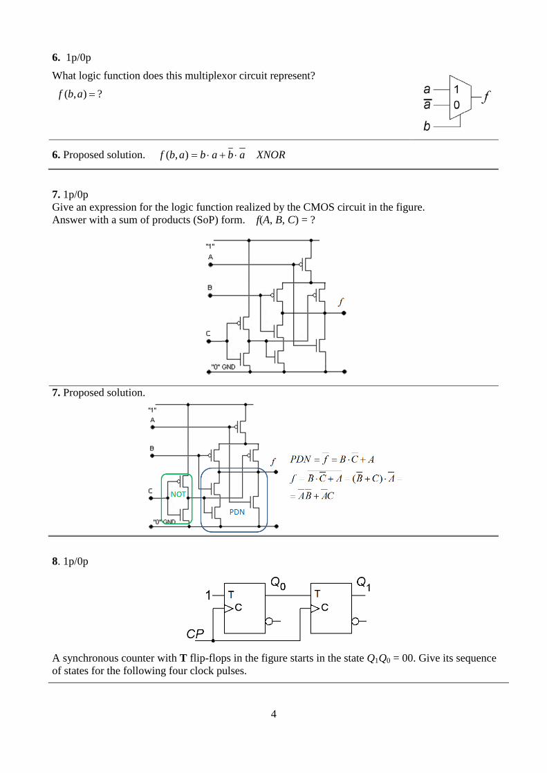
6. 1p/0p
What logic function does this multiplexor circuit represent?
?),( =abf
6. Proposed solution. XNORabababf ⋅+⋅=),(
7. 1p/0p Give an expression for the logic function realized by the CMOS circuit in the figure. Answer with a sum of products (SoP) form. f(A, B, C) = ?
7. Proposed solution.
8. 1p/0p
A synchronous counter with T flip-flops in the figure starts in the state Q1Q0 = 00. Give its sequence of states for the following four clock pulses.
5
8. Proposed solution.
Q0 toggles each clock pulse, Q1 toggles when Q0=1.
0011100100:01 →→→→QQ so, it acts as an ordinary binary counter. 9. 1p/0p
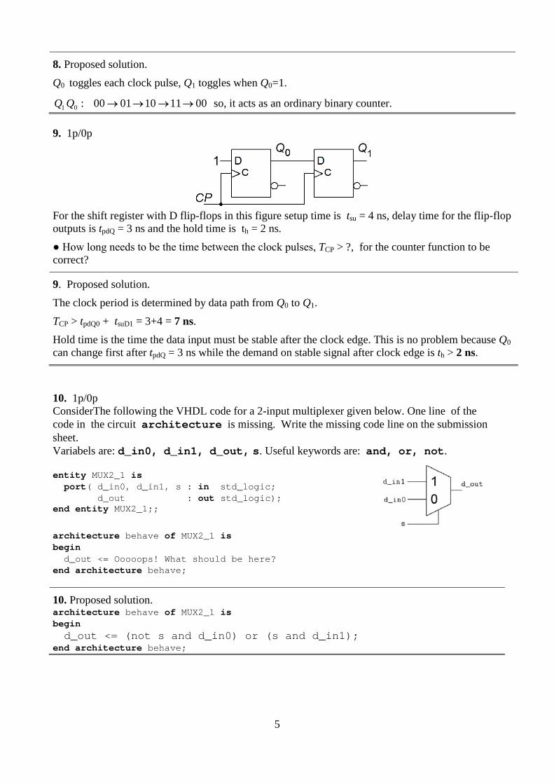
For the shift register with D flip-flops in this figure setup time is tsu = 4 ns, delay time for the flip-flop outputs is tpdQ = 3 ns and the hold time is th = 2 ns.
● How long needs to be the time between the clock pulses, TCP > ?, for the counter function to be correct?
9. Proposed solution.
The clock period is determined by data path from Q0 to Q1.
TCP > tpdQ0 + tsuD1 = 3+4 = 7 ns.
Hold time is the time the data input must be stable after the clock edge. This is no problem because Q0 can change first after tpdQ = 3 ns while the demand on stable signal after clock edge is th > 2 ns.
10. 1p/0p ConsiderThe following the VHDL code for a 2-input multiplexer given below. One line of the code in the circuit architecture is missing. Write the missing code line on the submission sheet. Variabels are: d_in0, d_in1, d_out, s. Useful keywords are: and, or, not. entity MUX2_1 is port( d_in0, d_in1, s : in std_logic; d_out : out std_logic); end entity MUX2_1;;
architecture behave of MUX2_1 is begin d_out <= Ooooops! What should be here? end architecture behave;
10. Proposed solution. architecture behave of MUX2_1 is begin d_out <= (not s and d_in0) or (s and d_in1); end architecture behave;
6
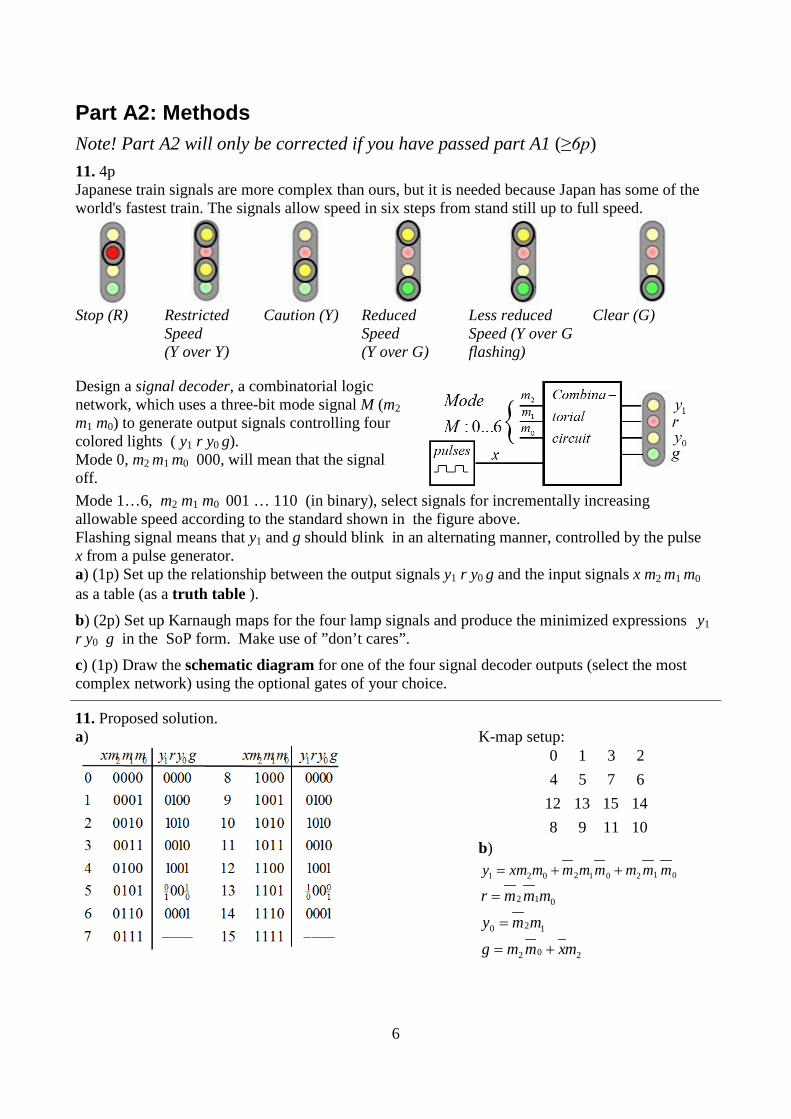
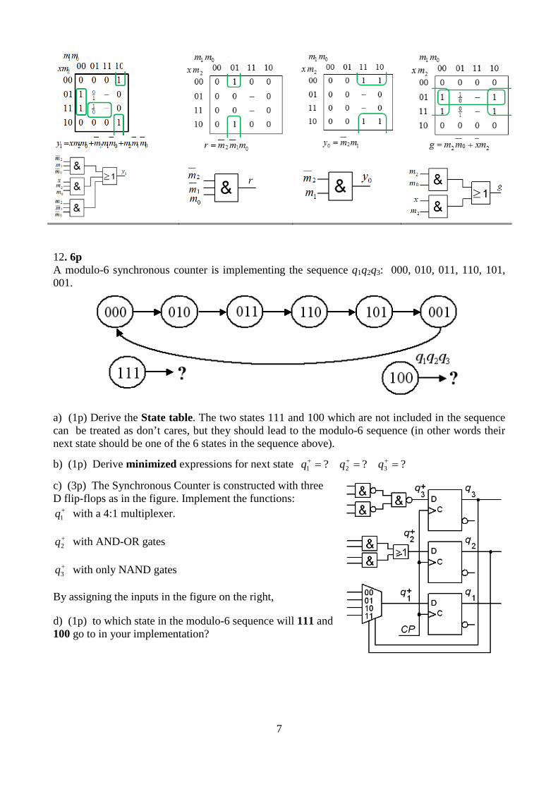
Part A2: Methods Note! Part A2 will only be corrected if you have passed part A1 (≥6p) 11. 4p Japanese train signals are more complex than ours, but it is needed because Japan has some of the world's fastest train. The signals allow speed in six steps from stand still up to full speed.
Stop (R) Restricted
Speed (Y over Y)
Caution (Y) Reduced Speed (Y over G)
Less reduced Speed (Y over G flashing)
Clear (G)
Design a signal decoder, a combinatorial logic network, which uses a three-bit mode signal M (m2 m1 m0) to generate output signals controlling four colored lights ( y1 r y0 g). Mode 0, m2 m1 m0 000, will mean that the signal off. Mode 1…6, m2 m1 m0 001 … 110 (in binary), select signals for incrementally increasing allowable speed according to the standard shown in the figure above. Flashing signal means that y1 and g should blink in an alternating manner, controlled by the pulse x from a pulse generator. a) (1p) Set up the relationship between the output signals y1 r y0 g and the input signals x m2 m1 m0 as a table (as a truth table ).
b) (2p) Set up Karnaugh maps for the four lamp signals and produce the minimized expressions y1 r y0 g in the SoP form. Make use of ”don’t cares”.
c) (1p) Draw the schematic diagram for one of the four signal decoder outputs (select the most complex network) using the optional gates of your choice.
11. Proposed solution. a)
K-map setup:
1011981415131267542310
b)
012012021 mmmmmmmxmy ++=
012 mmmr = 120 mmy =
202 mxmmg +=
7
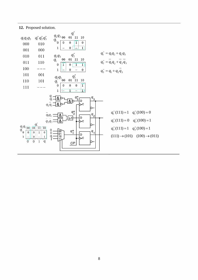
12. 6p A modulo-6 synchronous counter is implementing the sequence q1q2q3: 000, 010, 011, 110, 101, 001.
a) (1p) Derive the State table. The two states 111 and 100 which are not included in the sequence can be treated as don’t cares, but they should lead to the modulo-6 sequence (in other words their next state should be one of the 6 states in the sequence above).
b) (1p) Derive minimized expressions for next state ??? 321 === +++ qqq
c) (3p) The Synchronous Counter is constructed with three D flip-flops as in the figure. Implement the functions:
+1q with a 4:1 multiplexer.
+2q with AND-OR gates
+3q with only NAND gates
By assigning the inputs in the figure on the right,
d) (1p) to which state in the modulo-6 sequence will 111 and 100 go to in your implementation?
8
12. Proposed solution.
32211 qqqqq +=+
32212 qqqqq +=+
3213 qqqq +=+
0)100(1)111( 11 == ++ qq
1)100(0)111( 22 == ++ qq
1)100(1)111( 33 == ++ qq
)011()100()101()111( →→
9
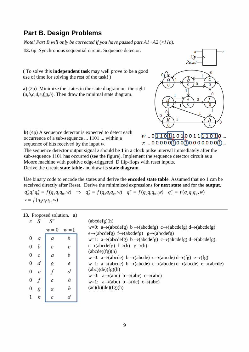
Part B. Design Problems Note! Part B will only be corrected if you have passed part A1+A2 (≥11p). 13. 6p Synchronous sequential circuit. Sequence detector.
( To solve this independent task may well prove to be a good use of time for solving the rest of the task! ) a) (2p) Minimize the states in the state diagram on the right (a,b,c,d,e,f,g,h). Then draw the minimal state diagram.
b) (4p) A sequence detector is expected to detect each occurrence of a sub-sequence ... 1101 ... within a sequence of bits received by the input w. The sequence detector output signal z should be 1 in a clock pulse interval immediately after the sub-sequence 1101 has occurred (see the figure). Implement the sequence detector circuit as a Moore machine with positive edge-triggered D flip-flops with reset inputs. Derive the circuit state table and draw its state diagram. Use binary code to encode the states and derive the encoded state table. Assumed that no 1 can be received directly after Reset. Derive the minimized expressions for next state and for the output.
),(),(),(),(),(
012
012001210122012012
wqqqfzwqqqfqwqqqfqwqqqfqwqqqfqqq
====⇒= ++++++
13. Proposed solution. a)
(abcdefg)(h) w=0: a→(abcdefg) b →(abcdefg) c→(abcdefg) d→(abcdefg) e→(abcdefg) f→(abcdefg) g→(abcdefg) w=1: a→(abcdefg) b →(abcdefg) c→(abcdefg) d→(abcdefg) e→(abcdefg) f→(h) g→(h) (abcde)(fg)(h) w=0: a→(abcde) b →(abcde) c→(abcde) d→(fg) e→(fg) w=1: a→(abcde) b →(abcde) c→(abcde) d→(abcde) e→(abcde) (abc)(de)(fg)(h) w=0: a→(abc) b →(abc) c→(abc) w=1: a→(abc) b →(de) c→(abc) (ac)(b)(de)(fg)(h)
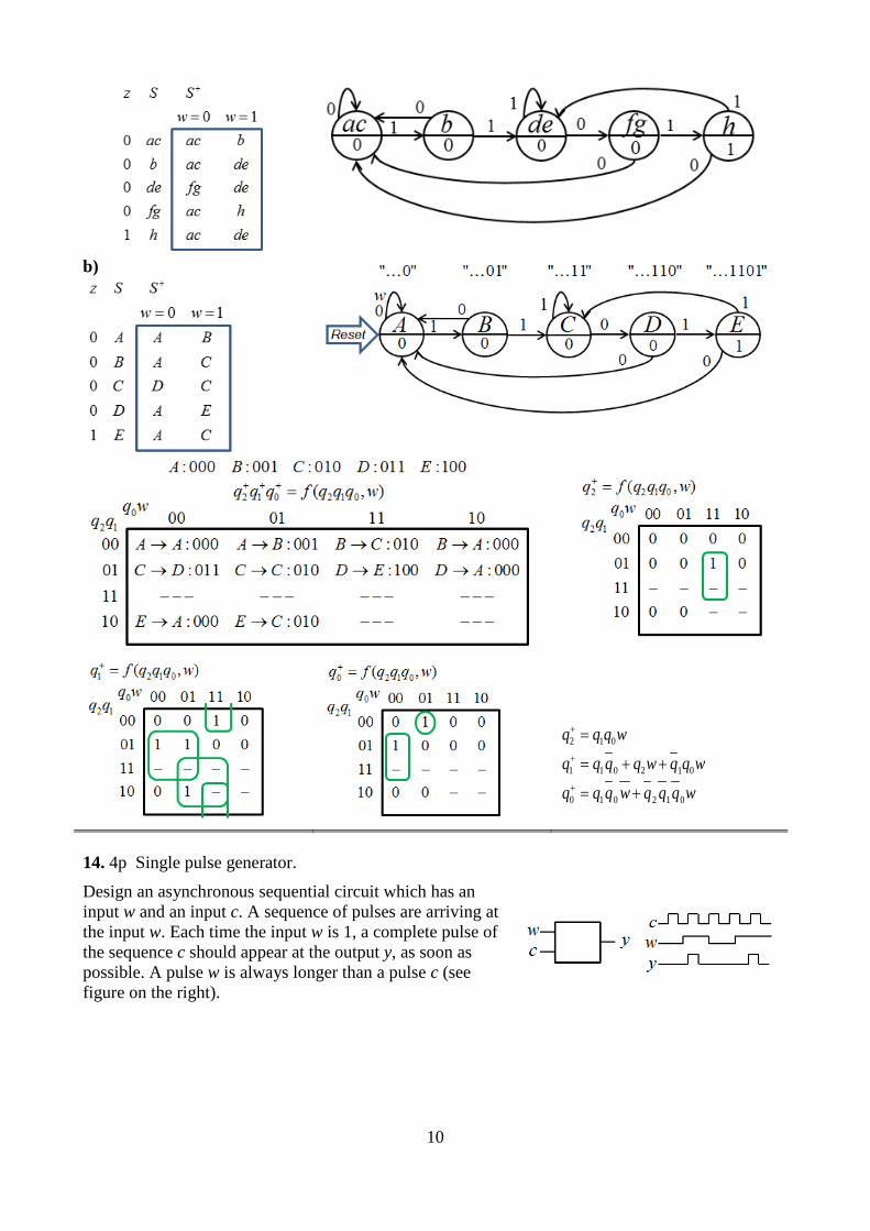
10
b)
2 1 0q q q w+ =
1 1 2 00 1q q q q w q q w+ = + +
0 1 0 2 1 0q q q w q q q w+ = +
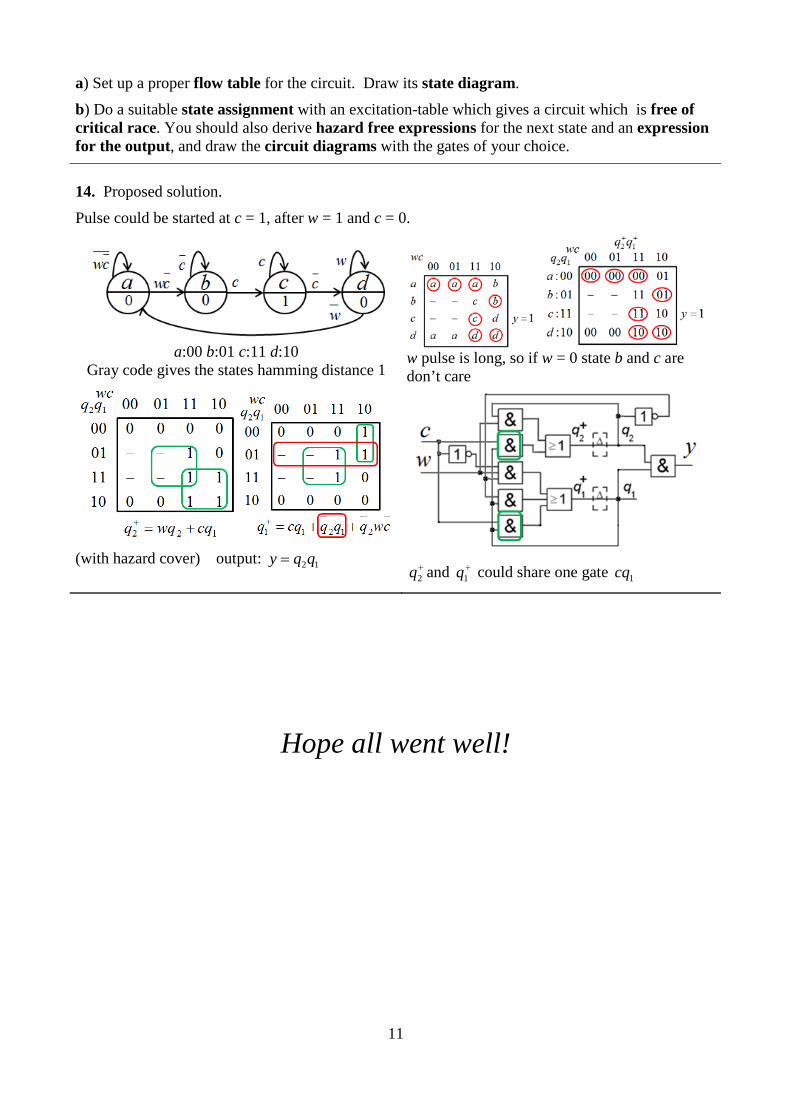
14. 4p Single pulse generator.
Design an asynchronous sequential circuit which has an input w and an input c. A sequence of pulses are arriving at the input w. Each time the input w is 1, a complete pulse of the sequence c should appear at the output y, as soon as possible. A pulse w is always longer than a pulse c (see figure on the right).
11
a) Set up a proper flow table for the circuit. Draw its state diagram.
b) Do a suitable state assignment with an excitation-table which gives a circuit which is free of critical race. You should also derive hazard free expressions for the next state and an expression for the output, and draw the circuit diagrams with the gates of your choice.
14. Proposed solution.
Pulse could be started at c = 1, after w = 1 and c = 0.
a:00 b:01 c:11 d:10
Gray code gives the states hamming distance 1
w pulse is long, so if w = 0 state b and c are don’t care
(with hazard cover) output: 12qqy =
+2q and +
1q could share one gate 1cq
Hope all went well!

12

13
Submission sheet for Part A1 Sheet 1 ( remove and hand in together with your answers for part A2 and part B )
Last name: Given name:
Personal code: Sheet: 1 Write down your answers for the questions from Part A1 ( 1 to 10 ) Question Answer
1 { } ?),,( min == SoPzyxf
2 s = K∙x x = 11112 s = ? [binary]
3 x = 0101 y = 0111 s = x+y ± s10 [ two complement number as signed decimal value]
4 ?}{),,,( min == PoSdcbaf
5 Q = f(A,B) = ?
6 ?),( =abf
7 f(A, B, C) = ?
8 →00:01 QQ
9 TCP > ? [ns]
10
architecture behave of MUX2_1 is begin
d_out <=
end architecture behave;
This table is completed by the examiner!! Part A1 (10) Part A2 (10) Part B (10) Total (30) Points 11 12 13 14 Sum Grade