wiserban · 2.1 d-bb implementation for the receiver ... 31 4 fpga implementation ... wp4 will...
TRANSCRIPT
FP7-ICT-2009-5 WiserBAN (257454) D4.2 V0.9
This project is funded by the European Commission under the 7th
Research Framework Programme.
WiserBAN
Project Acronym: WiserBAN
Project Title: Smart miniature low-power wireless microsystem for Body Area Networks
Call: FP7-ICT-2009-5, Collaborative project
Grant Agreement no.: 257454
Project Duration: 36 months
Coordinator: CSEM
Beneficiaries:
CSEM Centre Suisse D’Electronique et de Microtechnique SA – Recherche et Development
CSEM CH
Commissariat a L’Energie Atomique et aux Energies Alternatives CEA FR
Fraunhofer-Gesellschaft zur Foerderung der Angewandten Forschung E.V.
FRAUNHOFER DE
Valtion Teknillinen Tutkimuskeskus VTT FI
Technische Universitat Berlin TUB DE
Alma Mater Studiorum-Universita di Bologna UNIBO IT
Sorin CRM SAS SORIN FR
EPCOS SAS EPCOS FR
MED-EL Elektromedizinische Geraete GmbH MED-EL AT
Siemens Audiologische Technik GmbH DE-SAT DE
Debiotech S.A. DEBIOTECH CH
SignalGeneriX Ltd SG CY
RTD TALOS Ltd TALOS CY

FP7-ICT-2009-5 WiserBAN (257454) D4.2 V0.9
2
WiserBAN
Smart miniature low-power wireless microsystem for
Body Area Networks
Deliverable identifier: D4.2
Deliverable title: Characterization & Validation of the 1st
Base-Band version
Due date of deliverable: M18, February 29, 2012
Actual submission date: M21, May 21, 2012
Start day of project: 01/09/2010
Duration: 36 months
WP Number: WP 4 BAN MAC/Protocol and data processing
Organization name of lead partner for this deliverable (partner name): CEA
Author(s): L. Ouvry, F. Dehmas, E. Mercier. S. Thuries, M. Maman (CEA), C. Buratti, F.
Martelli, R. Rosini, R. Verdone (UNIBO), M-N. Morgan, D. Severac, E. Le Roux (CSEM), K.
Michaelides, D. Doumenis (SG)
Document Status: Delivered
Project funded by the European Commission within the Seventh Framework Programme
Dissemination Level
PU Public
PP Restricted to other programme participants (including the Commission Services)
RE Restricted to a group specified by the consortium (including the Commission Services)
CO Confidential, only for members of the consortium (including the Commission Services) x
FP7-ICT-2009-5 WiserBAN (257454) D4.2 V0.9
3
Revision History
Version Date Changed page(s) Cause of change Partner
V0.1 Mar 05 2012 Creation CEA
V0.2 Mar 19 2012 Section 3 & 5 have been integrated
CEA, SG
V0.3 Mar 21 2012 Section 6 has been integrated
Uni Bo, CEA
V0.4 Mar 27 2012 Introduction & conclusion
CEA
V0.5 Apr 5 2012 Modified contribution CSEM & UNIBO
V0.6 Apr 9 2012 Pre-final review CSEM
V0.7 Apr 17 2012 Latest contributions & improvements
CEA
V0.8 Apr 27 2012 Latest contributions from CSEM
CSEM
V0.9 May 21 2012 Final review before submission
CSEM
Disclaimer: The information in this document is subject to change without notice. Company
or product names mentioned in this document may be trademarkers or registered
trademarks of their respective companies.
All rights reserved.
The document is proprietary of the WiserBAN consortium members. No copying or
distributing, in any form or by any means is allowed without the prior written agreement of
the owner of the property rights.
Τhis document reflects the authors’ view. The European Community is not liable for any use
that may be made of the information contained herein.

FP7-ICT-2009-5 WiserBAN (257454) D4.2 V0.9
4
Contents
Contents ............................................................................................................... 4
Executive Summary ............................................................................................... 6
1 Introduction ................................................................................................... 7
1.1 Goals and methodology ..................................................................................... 7
1.2 Digital system to validate .................................................................................. 7
2 Digital BaseBand validation ........................................................................... 9
2.1 D-BB implementation for the receiver ................................................................ 9
2.2 D-BB RX test methodology and validation ........................................................ 12
2.3 D-BB implementation for the transmitter......................................................... 20
2.4 D-BB TX test methodology and validation ........................................................ 25
3 Processor unit validation ............................................................................... 27
3.1 Pre-integration validation ................................................................................ 27
3.2 Post-integration validation of the functionality ................................................ 27
3.3 Released package of the processor unit for the FPGA validation ....................... 31
4 FPGA implementation ................................................................................... 32
4.1 General architecture ....................................................................................... 32
4.1.1 Hardware Used ................................................................................................................. 32
4.1.2 Programming the icyflex core into the FPGA .................................................................... 34
4.2 Methodology for the validation of the SoC complete digital ............................. 37
4.3 Results of the FPGA validation ......................................................................... 40
4.3.1 Synthesized D-BB Rx VHDL Code Validation ..................................................................... 41
4.3.2 Synthesized icyflex VHDL Code Validation ........................................................................ 43
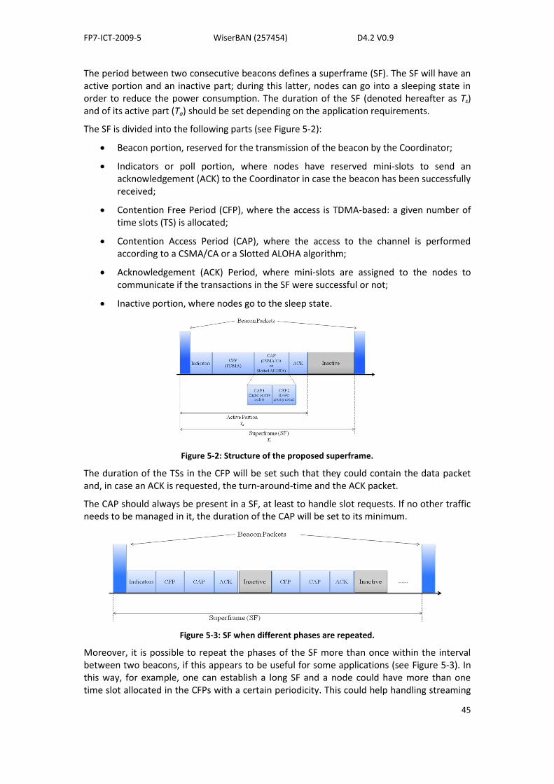
5 BAN specific protocol implementation and validation .................................... 44
5.1 General description of the protocol ................................................................. 44
5.2 Simulation results related to propagation measurements ................................ 46
5.2.1 Measurements set ............................................................................................................ 46
5.2.2 Simulation settings and scenario ...................................................................................... 47
5.2.3 Simulation Results ............................................................................................................ 49
5.2.4 Conclusions ....................................................................................................................... 56
5.3 BAN Protocol implementation ......................................................................... 57
5.3.1 The Software Architecture ................................................................................................ 57
5.3.2 The Software Implementation .......................................................................................... 66

FP7-ICT-2009-5 WiserBAN (257454) D4.2 V0.9
5
6 Conclusions ................................................................................................... 68
7 Annexes ........................................................................................................ 69
7.1 List of Tables ................................................................................................... 69
7.2 List of Figures .................................................................................................. 70
7.3 List of references ............................................................................................. 73
7.4 Abbreviations .................................................................................................. 73
FP7-ICT-2009-5 WiserBAN (257454) D4.2 V0.9
6
Executive Summary
The WiserBAN project will create an ultra-miniature and ultra low-power RF microsystem for wireless Body Area Networks (BAN) targeting primarily wearable and implanted devices for healthcare, biomedical and lifestyle applications. The proposed research concerns the extreme miniaturization of the BAN with primarily the areas of ultra low-power radio SoC (System on Chip), RF and Low-frequency MEMS, miniature reconfigurable antennas, miniaturized SiP (System in Package), sensor signal processing and flexible communication protocols. The WiserBAN microsystem will be 50 times smaller than today’s radio modules for Personal Area Networks (PAN) solutions, e.g. Bluetooth, that can simply not be embedded in a variety of tiny implants and wearable applications. WiserBAN will thus enable significant take up by the European SME’s and industries in healthcare, bio-medical and lifestyle. WiserBAN will also create a major impact on the quality of life of the European Citizens, in particular for improving the comfort and access to ICT for impaired and disabled people of all ages carrying implants or wearing medical devices, hence reducing the risk of social exclusion. WP4 will consist in the design, simulation and validation of the digital part of the BAN radio microsystem, which entails the radio transceiver baseband, MAC units (soft & hard), and the sensor data processing unit. About this deliverable D4.2: This deliverable is the second one of the WP4 within the WiserBAN project, and concerns all the tasks T4.1, T4.2 and T4.3 which are:
• Task 4.1 Reconfigurable Baseband and MAC objectives:
Design and develop both the baseband and the hardware MAC entities to be attached to the smart RF components which WP2 will provide, Design reconfigurable MAC entities, through reprogramming, for greater flexibility in the applications requirements/constraints that WiserBAN will address.
• Task 4.2 Low Power BAN Protocol objectives:
Design an energy efficient BAN protocol architecture with the support for various applications requirements (variable data-rates, quality-of-service, reliability, priorities, directions of flows, etc.) and the support of coexistence, cooperation and compliance with existing BAN/PAN architectures.
• Task 4.3 Low-power sensor data processing unit objectives:
Develop and integrate a high-performance, low-power, DSP-based unit at the core of the application layer. This DSP-based unit will be in charge of Running the basic MAC protocol (T4.2) and controlling the interfaces with the other system or applicative parts. The application data processed by this unit will be used to feed the MAC layer below it.
It shall link the applications, scenarios, and platform requirements from WP1 to the research done within WP4 on the MAC protocol and the reconfigurable digital baseband. In particular, requirements on the quality of services to comply with the different scenarios shall be analysed from the protocol perspective, taking into account existing standards like Bluetooth Low Energy or IEEE802.15.6. The objective is in a first place to provide solutions as much as possible compliant with standards or to justify proprietary choices.
FP7-ICT-2009-5 WiserBAN (257454) D4.2 V0.9
7
1 Introduction
1.1 Goals and methodology
The D4.2 deliverable goals are:
To provide characterization and validation results of the digital blocks which have
been designed in the scope of the implementation into the WiserBAN SoC.
To validate the methodology for the validation of the digital blocks and settle a high
level of confidence in the developed blocks for an expected successful SoC release.
To demonstrate the good interoperability of the various blocks designed by the
partners in different places.
To elaborate and validate by simulation a complete protocol including outcomes from
around-the-body propagation measurements.
The deliverable content is organized accordingly with sections addressing:
the VHDL code development for the D-BB Rx and Tx, and for the icyflex DSP processor
and associated peripherals,
the validation of these codes on a high-level simulation platform,
the validation of digital part integrated into MPW1 SoC,
the validation of these codes on a FPGA platform,
the implementation of the associated protocol taking into account the specific BAN
environment.
The different validations described above are covering different parts with different
coverage limitations that are explained in respective sections. The limitations are linked to a
usual effort-coverage trade off. But finally, the validation must provide a good confidence on
digital system integration quality.
1.2 Digital system to validate
The purpose of section 2 is to introduce from a high-level the architecture of the building
blocks described hereafter. They include the D-BB Rx and D-BB Tx, the interface to the icyflex
and some elements to build a HW MAC, the icyflex itself and the implementation of the
whole onto an FPGA platform, and the context of the related protocols using outcomes from
propagation measurements. In this deliverable, characterization elements and validation
process resulting from dedicated tests are introduced and detailed.

FP7-ICT-2009-5 WiserBAN (257454) D4.2 V0.9
8
The implementation of the WiserBAN digital system includes the Tx and Rx Digital BaseBand
which processes the received signal and manages the low-level protocol elements, the
processor which supports the software of application and high-level protocol elements.
Regarding the D-BB Rx, it is composed of many different blocks, derived from the algorithms
to down convert the signal to Base-Band, filter it out, and finally demodulate the
information. The inputs of this part are made of bits from the Anolog-to-Digital Converter,
directly from the analog domain. The outputs are packaged into buffers, registers and are
also signals like interrupts in a format which is compatible with the processor. This part has
yet not been integrated into the first SoC, so the validation which is provided with here in
this deliverable is based on high-level simulations experiencing various scenarii of interest.
These simulations are optimized to limit the dead zone, where validation is missing and
remaining errors or mismatches may be uncharacterized. This is described in Section 3.
On the D-BB Tx side, a similar approach has also been considered. The inputs come from the
processor through registers and the output consists in the modulation of the RF signal by
dynamic digital control of the RF synthesizer. Some interrupts are also generated to inform
the processor about the status of the transmission. This is described in Section 3.
Once the VHDL code has been generated and validated in-depth, it is also possible to
consider its implementation on an actual hardware platform like an FPGA. This is done
thanks to a specific development which will also be of interest for the implementation of the
application software and protocol before the final SoC is ready. Thereby, the correctness of
the connectivity between the various blocks – D-BB Rx and Tx, icyflex core, IRQ manager,
icyflex bus – can be confirmed in an alternative manner to the simulation one. The
implementation of this hardware platform and its use is described in the Section 5.
As above-described, the principle of the characterization and validation of the digital blocks
is also applied to the protocol elements. It is based on codes which have been developed
taking into account actual conditions related to BAN propagation. First, simulations are
carried out to validate the interest of this dedicated protocol, and second its further
preliminary implementation onto a hardware target will help to finalize and refine it before
it is used into the final WiserBAN module. To this end, the Icycom platform has been chosen
as it integrates an icyflex core and an associated RF transceiver (not carrier frequency and
data rate compatible). In Section 6 is detailed the implementation of the protocol and its
validation on a simulation platform.
FP7-ICT-2009-5 WiserBAN (257454) D4.2 V0.9
9
2 Digital BaseBand validation
This section describes the D-BB Rx and Tx in a straightforward way, and detail the validation
methodology as well as the simulation & measurements results obtained using an adequate
set of test benches and simulation environment.
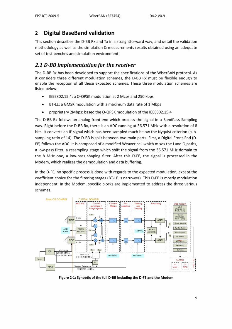
2.1 D-BB implementation for the receiver
The D-BB Rx has been developed to support the specifications of the WiserBAN protocol. As it considers three different modulation schemes, the D-BB Rx must be flexible enough to enable the reception of all these expected schemes. These three modulation schemes are listed below:
IEEE802.15.4: a O-QPSK modulation at 2 Mcps and 250 kbps
BT-LE: a GMSK modulation with a maximum data rate of 1 Mbps
proprietary 2Mbps: based the O-QPSK modulation of the IEEE802.15.4
The D-BB Rx follows an analog front-end which process the signal in a BandPass Sampling
way. Right before the D-BB Rx, there is an ADC running at 36.571 MHz with a resolution of 8
bits. It converts an IF signal which has been sampled much below the Nyquist criterion (sub-
sampling ratio of 14). The D-BB is split between two main parts. First, a Digital Front-End (D-
FE) follows the ADC. It is composed of a modified Weaver cell which mixes the I and Q paths,
a low-pass filter, a resampling stage which shift the signal from the 36.571 MHz domain to
the 8 MHz one, a low-pass shaping filter. After this D-FE, the signal is processed in the
Modem, which realizes the demodulation and data buffering.
In the D-FE, no specific process is done with regards to the expected modulation, except the
coefficient choice for the filtering stages (BT-LE is narrower). This D-FE is mostly modulation
independent. In the Modem, specific blocks are implemented to address the three various
schemes.
Figure 2-1: Synoptic of the full D-BB including the D-FE and the Modem

FP7-ICT-2009-5 WiserBAN (257454) D4.2 V0.9
10
The overall D-BB is monitored and controlled thanks to configuration registers which are
directly connected to the icyflex internal bus. It also provides with Interruptions to enable an
easy handling of the communications. These have been designed in relation with the icyflex
architecture and use the Interrupt manager of the processor.
Figure 2-2: synoptic of the full-Digital BaseBand
Clocks are provided by the frequency reference based on the 2.048 GHz BAW oscillator.
After the signal has been resampled in the D-FE, it is processed by an 8 MHz clock
synchronized with the 32 MHz one used in the digital and specifically in the processor.
At the end of the D-BB Rx, the data are buffered in a dedicated buffer which can contain the
maximum number of octets specified in a frame - 128 octets.
In addition to this functional architecture of the D-BB Rx, some test modes have been added.
They are of three kinds. On one hand, some passive test modes can be used. For instance,
the configuration of the blocks can be tuned thanks to the configuration registers. They can
be used for instance to fine tune the level of signal which will trigger a synchronization
process on the Modem or modify some gain in the chain. Once these parameters have been
tested and optimized, they can be documented and the embedded software, using libraries,
can set these up, and therefore optimize the functioning of the receiver. The Interrupts
signal can also be used as validation and test signal as they propose real-time activation
monitoring to known stimuli. On the other hand, active test modes have been implemented
to validate the correct functioning of the D-BB Rx, besides try to find out where in the chain
any mismatch or issue may be generated. To do so, monitoring the signal at different levels
or inject specific signals through registers has been made possible and loop-back techniques
employed.
All the D-BB Rx registers are listed below:

FP7-ICT-2009-5 WiserBAN (257454) D4.2 V0.9
11
Address Register R/W Size Default Description
0x00 to 0x1F: D-BB_RX registers
0x00 DBB_RX_CTRL R/W 16 0x0 Control register
0x02 DBB_RX_STATUS R 16 0x0 DBB_RX status register
0x04 DBB_RX_DEBUG R/W 8 0x0 Reserved for programmable states enabling internal
connections
0x05 DBB_RX_IRQ_ACK R/W 8 0x0 Interrupt acknowledge register
0x06 DBB_RX_IRQ_STATUS R 16 0x0 Interrupt status register
0x08 DBB_RX_IRQ0_EN R/W 16 0x0 IRQ0 Interrupt mask register
0x0A DBB_RX_IRQ1_EN R/W 16 0x0 IRQ1 Interrupt mask register
0x0C DBB_RX_IRQ2_EN R/W 16 0x0 IRQ2 Interrupt mask register
0x0E DBB_RX_FIFO_RX_THRES R/W 8 0x0 Programmable threshold for the FIFO RX
0x10 DBB_RX_FIFO_LOOPBACK_DATA_0 R/W 16 0x0 Loopback mode (to DFE or DBB depending mode selected
in DBB_RX_CTRL)
0x12 DBB_RX_FIFO_LOOPBACK_DATA_1 R/W 16 0x0 Same as DBB_RX_FIFO_LOOPBACK_DATA_1 but generate
one pulse in CLK_36M
0x14 DBB_RX_FIFO_RX_DATA R 32 0x0 DATA from FIFO RX in normal mode (selected in
DBB_RX_CTRL)
0x18 DBB_RX_FIFO_LOOPBACK_DUMP R 32 0x0 Output data dump (from ADC or DFE depending mode
selected in DBB_RX_CTRL)
0x1C DBB_RX_VENDOR_ID R 32 0x0 Vendor ID register
0x20 to 0x2F: D-FE registers
0x20 DBB_RX_DFE_CTRL R/W 16 0x0 Control register
0x22 DBB_RX_DFE_AFE_AGC_THRES R/W 8 0x0 AFE AGC threshold
0x23 DBB_RX_DFE_RES_AGC_THRES R/W 8 0x0 Rescale AGC threshold
0x24 DBB_RX_DFE_RSSI_DIV R/W 8 0x0 Select averaging value for RSSI
0x25 DBB_RX_DFE_RSSI_FRAME R/W 8 0x0 RSSI in the received frame
0x26 DBB_RX_DFE_RSSI_VALUE R/W 8 0x0 Current RSSI
0x30 to 0x3F: IEEE802.15.4 modem registers
0x30 DBB_RX_RX1_SFD_WORD R/W 8 0xA7 SFD Byte
0x31 DBB_RX_RX1_SYNCH R/W 8 0x5 SYNC_TH synchronization detection threshold
0x32 DBB_RX_RX1_CPT_THRES R/W 8 0x6 -

FP7-ICT-2009-5 WiserBAN (257454) D4.2 V0.9
12
0x33 DBB_RX_RX1_GAIN_THRES R/W 8 0x8D Gain for the RX demodulation algorithm
0x34 DBB_RX_RX1_LQI_VALUE R 8 0x0 Link quality indicator result
0x35 DBB_RX_RX1_PHR_VALUE R 8 0x0 PHR value
0x36 DBB_RX_RX1_CRC_VALUE R 16 0x0 CRC value
Table 1: D-BB Rx registers
To use the loopback functionality, a specific mode has to be selected. It is then possible, in
simulation as with the actual SoC, to inject frames into the D-BB Rx and monitor the output
to verify the correct processing in the D-FE as well as in the Modem.
2.2 D-BB RX test methodology and validation
The methodology for the validation of the full D-BB Rx is based on being able to stick the
behaviour when simulating to the actual behaviour of the final SoC. To do so, the entry
points and outcomes of the test process have been limited to the minimum. A test bench is
set around the core D-BB Rx VHDL featuring a 2 entry points:
ADC output / input of D-FE
icyflex bus
which are fed by input files generated using Matlab, and 2 possible outputs:
Data buffer: directly readable by the icyflex interface
Spy block in the test bench: automatically generating files fed with the outputs of each D-BB Rx constituting block
This way, the D-BB Rx is not impacted by the requirements of the test hardware as it uses
features already available for the SoC functioning.
From this methodology, several scenarii have been envisioned in simulation to validate the
correctness of the whole D-BB Rx. They are all related to test modalities of interest to detect
potential sources of non-functioning.

FP7-ICT-2009-5 WiserBAN (257454) D4.2 V0.9
13
Figure 2-3: test bench interface with the D-BB Rx
The architecture of this test bench allows monitoring the signal on the complete D-BB Rx
chain. The signals are stored into files which can be compared to expectation files devised
thanks to Matlab.
At the end of the D-BB Rx chain, it is also possible to read the data buffer and get the
received, which can then be compared with the original data bytes file used to generate the
Matlab log file.
Given this methodology, various test can be carried out. Amongst them, some can be
described as functional tests as they are carried out using ideal waveform processed under
Matlab. The list below describes these functional tests:
Name of the test Description
rx/F000_802_15_4_full_decodage This validates the whole IEEE802.15.4 modem, for 100
packets fo 20 bytes each at an expected received power
of -85 dBm and a CFO of 20 ppm.
rx/F001_dfe_802_15_4_adc_input This validates the D-FE only in the normal mode, with a
pulse shaping filter set for IEEE802.15.4
rx/F002_dfe_802_15_4_adc_sat_input This validates the D-FE only in the normal mode with
generated saturated data at the input from the ADC,
with a pulse shaping filter set for IEEE802.15.4
rx/F003_dfe_bluetooth_adc_input This validates the D-FE only in the normal mode with a
pulse shaping filter set for BlueTooth LE 1Mbps
rx/F004_dfe_bluetooth_adc_sat_input This validates the D-FE only in the normal mode with
generated saturated data at the input, with a pulse
FP7-ICT-2009-5 WiserBAN (257454) D4.2 V0.9
14
shaping filter set for BlueTooth LE 1Mbps
rx/F005_IRQ _end_frame This validates the interrupt end_frame on IRQ0, IRQ1,
IRQ2
rx/F006_IRQ_fifo_rx_full This validates the interrupt fifo_rx_full on IRQ0, IRQ1
and IRQ2
rx/F007_IRQ_fifo_rx_part This validates the interrupt fifo_rx_part on IRQ0, IRQ1
and IRQ2, for DBB_RX_FIFO_THRES = 3
rx/F008_IRQ_fifo_rx_empty This validates the interrupt fifo_rx_empty on IRQ0 and
IRQ1
rx/F009_IRQ_fifo_rx_underflow This validates in the loopback mode the interrupt
fifo_rx_underflow on IRQ0 and IRQ1
rx/F010_IRQ_fifo_rx_overflow This validates the interrupt fifo_rx_overflow on IRQ0
rx/F011_IRQ_fifo_adc_overflow This validates in the loopback mode the interrupt
fifo_adc_overflow on IRQ0.
rx/F012_IRQ_end_frame_loopback_dfe_input This validates in the loopback mode the interrupt
end_frame on IRQ0, IRQ1 and IRQ2
rx/F013_IRQ_fifo_rx_full_loopback_ dfe_input This validates in the loopback mode the interrupt
fifo_rx_full on IRQ0, IRQ1 and IRQ2
rx/F014_IRQ_fifo_rx_part_loopback_ dfe_input This validates in the loopback mode the interrupt
fifo_rx_part on IRQ0, IRQ1 and IRQ2
rx/F015_IRQ_fifo_rx_empty_loopback_ dfe_input This validates in the loopback mode the interrupt
fifo_rx_empty on IRQ0, IRQ1 and IRQ2
rx/F016_IRQ_fifo_rx_underflow_loopback_ dfe_input This validates in the loopback mode the interrupt
fifo_rx_underflow on IRQ0 and IRQ1
rx/F017_IRQ_fifo_rx_overflow_loopback_ dfe_input This validates in the loopback mode the interrupt
fifo_rx_overflow on IRQ0
rx/F018_RSSI_AFE_AGC_16_RSSI_rescale_AGC_8 This validates the RSSI value calculated for AFE_AGC at
16 and rescale_AGC at 8
rx/F019_RSSI_AFE_AGC_32_RSSI_rescale_AGC_16 This validates the RSSI value calculated for AFE_AGC at
32 and rescale_AGC at 16
rx/F020_RSSI_AFE_AGC_64_RSSI_rescale_AGC_32 This validates the RSSI value calculated for AFE_AGC at
64 and rescale_AGC at 32
rx/F021_RSSI_AFE_AGC_128_RSSI_rescale_AGC_64 This validates the RSSI value calculated for AFE_AGC at
128 and rescale_AGC at 64
rx/F022_RSSI_AFE_AGC_256_RSSI_rescale_AGC_128 This validates the RSSI value calculated for AFE_AGC at
256 and rescale_AGC at 128
rx/F023_RSSI_AFE_AGC_512_RSSI_rescale_AGC_256 This validates the RSSI value calculated for AFE_AGC at
512 and rescale_AGC at 256
rx/F024_RSSI_AFE_AGC_1024_RSSI_rescale_AGC_512 This validates the RSSI value calculated for AFE_AGC at
1024 and rescale_AGC at 512

FP7-ICT-2009-5 WiserBAN (257454) D4.2 V0.9
15
rx/F025_RSSI_AFE_AGC_2048_RSSI_rescale_AGC_1024 This validates the RSSI value calculated for AFE_AGC at
2048 and rescale_AGC at 1024
rx/F026_rescale_AGC_auto_mode This validates the behaviour of the automatic rescale
driven by the AGC block
rx/F027_loopback_dfe_input This validates the D-FE only in the loopback mode. The
input data are coming at the input of the D-FE through
the icyflex data bus.
rx/F028_loopback_modem_input This validates the IEEE802.15.4 Modem only in the
loopback mode. The input data are coming at the input
of the Modem through the icyflex data bus. The
decoded bytes are buffered and read thanks to the
fifo_rx_full IT.
rx/F029_dump_adc_output This monitors the data directly at the output of the ADC.
It will be useful to test and characterize the ADC
functioning on the actual SoC implementation
rx/F030_dump_dfe_output This monitors the data directly at the output of the DFE.
It will be useful to test and characterize the DFE
functioning on the actual SoC implementation
rx/F031_loopback_dfe_input_dump_dfe_output This monitors the data directly at the output of the DFE
while injecting the data stream at its imput. It will be
useful to test and characterize the DFE functioning on
the actual SoC implementation
rx/F032_swap_cos_I_FI2BB_input This tests the inversion of sign on cosine I path
rx/F033_swap_sin_I_FI2BB_input This tests the inversion of sign on sine I path
rx/F034_swap_cos_Q_FI2BB_input This tests the inversion of sign on cosine Q path
rx/F035_swap_sin_Q_FI2BB_input This tests the inversion of sign on sine I path
rx/F036_CRC_normal_mode This validates the CRC functioning. The frame is
removed if the CRC is wrong.
rx/F037_CRC_debug_mode This validates the CRC functioning. The frame is kept
even if the CRC is wrong.
rx/F038_IRQ_dfe_res_agc_sat This valides in the norrmal mode the interrupt
dfe_res_agc_sat on IRQ0, IRQ1 and IRQ2
rx/F039_IRQ_dfe_res_agc_sat_loopback_dfe_input This valides in the loopback mode the interrupt
dfe_res_agc_sat on IRQ0, IRQ1 and IRQ2
Table 2: Functional tests carried out on the D-BB Rx
The first ones are investigating the correctness of the D-FE for the 2 Pulse Matched filter
configurations, corresponding to the IEEE802.15.4 and BT-LE versions of the filter.
When loopback is mentioned, the tests verify the correctness of the D-FE and the Modem by
injecting the data through the icyflex bus: this verifies at the same time the validity of the
bus interface and of the loopback mode.

FP7-ICT-2009-5 WiserBAN (257454) D4.2 V0.9
16
When the ADC is mentioned, the values of interest are fed thanks to the loopback mode,
and read through the icyflex bus. This eases the validation of the ADC, without passing the
signal through the D-BB.
Indeed, the target for these tests is to match to output files with the files generated by the
algorithms simulated with Matlab. Finally, all these tests described here have been passed
successfully and no issue has been found. It also has to be mentioned that most of these
tests monitor intermediate files in the chain. These intermediate files also exhibit correct
result which validates the overall test bench methodology and secure the porting of the
VHDL code to the SoC implementation.
Another feature which is also tested carefully in the previous tests is the interrupt
generation one. When generating and simulating the proposed scenario, the activation of
interrupts of interest has also been activated. Some screen snapshots of the simulations are
presented below to explain how and when the interrupts are generated.
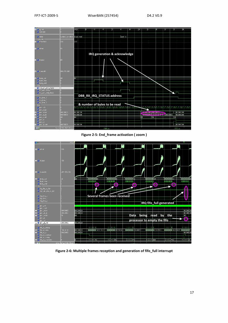
Figure 2-4: frame reception and end_frame IT generation
Length of the frame = 20 bytes
IRQ activation
Bytes received and buffered
FP7-ICT-2009-5 WiserBAN (257454) D4.2 V0.9
17
Figure 2-5: End_frame activation ( zoom )
Figure 2-6: Multiple frames reception and generation of fifo_full interrupt
DBB_RX_IRQ_STATUS address
& number of bytes to be read
IRQ generation & acknowledge
IRQ fifo_full generated
Several frames been received
Data being read by the
processor to empty the fifo

FP7-ICT-2009-5 WiserBAN (257454) D4.2 V0.9
18
Figure 2-7: Frame reception and fifo_full interrupt generation ( zoom )
Figure 2-8: Frame reception and generation of a FIFO partial filling interrupt
IRQ fifo_full generated on IRQ0
DBB_RX_FIFO_RX_DATA address &
RX data been read by the processor
128 bytes read by packets of 32 bits
32 read sequences
IRQ fifo_part generated
Several frames been received
Data being read from
the fifo by the processor

FP7-ICT-2009-5 WiserBAN (257454) D4.2 V0.9
19
Figure 2-9: Frame reception and generation of the fifo_part IT ( zoom )
These display the correctness of the IT generation process. As explained, all the IT developed
with the overall D-BB have been tested and validated when simulating the reception of the
frames.
Some performance tests have also been carried out to validate that in real conditions, the
frame would be received in a correct manner. As a first step, the robustness to frequency
drift has been considered. Due to the long possible received frame, it is mandatory to
confirm that the frequency difference between the receiver module and the transmitter will
not create an error in the demodulation.
Name of the test Description
rx/P000_FRAME80_PHR127_-80to80ppm_85dbm This validates the Compensation of Frequency
Offset for IEEE802.15.4, with 80 packets of 127
bytes payload at a received power of -85 dBm,
considering 2 ppm steps between 2 packets to
finally civer +/-80 ppm drift.
rx/P001_FRAME123_PHR5to127_20ppm_85dbm This validates the Compensation of Frequency
Offset for IEEE802.15.4, for packets of PHR
between 5 and 127 bytes, at a received power
of -85 dBm, considering 20 ppm drifts.
rx/P002_FRAME31_PHR20_80ppm_95dbm This validates the correct reception of 31
frames of 20 bytes at an equivalent level of -95
dBm signal with a CFO of 80 ppm for
IEEE802.15.4.
rx/P003_FRAME2_PHR_with_zero_80ppm_85dbm This validates the correct reception of 2 frames
of 0 bytes at an equivalent level of -85 dBm
signal with a CFO of 80 ppm for IEEE802.15.4.
The purpose is to make sure that no weird
IRQ fifo_part generated
on IRQ0
DBB_RX_FIFO_RX_DATA
address & RX data been
read by the processor

FP7-ICT-2009-5 WiserBAN (257454) D4.2 V0.9
20
behaviour happens when sequences of zero is
received.
rx/P004_RX1_FRAME40_random_PHR_CFO_Prx_test0 This validates the correct reception of frames
with random PHR, recoeved signal level, and
CFO. 40 packets with a payload between 5 and
127, a power level between -20 and -95 dBm,
and a drift between -80 and +80 ppm.
rx/P005_RX1_FRAME40_random_PHR_CFO_Prx_test1 This validates the correct reception of frames
with random PHR, recoeved signal level, and
CFO. 40 packets with a payload between 5 and
127, a power level between -20 and -95 dBm,
and a drift between -80 and +80 ppm.
rx/P006_RX1_FRAME40_random_PHR_CFO_Prx_test2 This validates the correct reception of frames
with random PHR, recoeved signal level, and
CFO. 40 packets with a payload between 5 and
127, a power level between -20 and -95 dBm,
and a drift between -80 and +80 ppm.
rx/P007_RX1_FRAME40_random_PHR_CFO_Prx_test3 This validates the correct reception of frames
with random PHR, recoeved signal level, and
CFO. 40 packets with a payload between 5 and
127, a power level between -20 and -95 dBm,
and a drift between -80 and +80 ppm.
rx/P008_RX1_FRAME50_PHR20_20ppm_variable_spacing This validates the correct reception of frames
with random spacing between them. The PHR is
20 bytes and the power level -95 dBm. 50
packets are simulated.
Table 3: Performance tests carried out on the D-BB Rx
A Compensation of Frequency Offset has been implemented, and the validation tests have
demonstrated that it was not robust enough to support 80 ppm drift. Thereby, the VHDL
code has been modified in order to improve this and it can now support more than 80 ppm
(or +/- 40 ppm on each side of the RF link). Finally, the test bench has demonstrated that a
full 127-byte frame was received correctly even in the case of +/- 80 ppm drifts. It has also
been tested in the case of various frame lengths, at the minimum expected power level, with
successful results.
The validation of DFE, for all targeted modulations, and demodulation of 802.15.4 as well as
interface with the icyflex bus has been performed by simulation. Because the associated
digital functionality will be integrated in silicon in MPW2, those validations will be reinforced
by measurement before final integration. The validation of remaining demodulations will be
performed following the same flow with the addition of a validation by measurement before
final integration using the FPGA platform described in chapter 4.
2.3 D-BB implementation for the transmitter
The modulation is realized by direct dynamic digital programming of the Tx VCO, running at
the output frequency. Basically, the sample rate at the output of the modulator is x8 times
the symbol rate, the closed-loop transfer function realizing the interpolation filter. This is
enough in practice to get alias below the phase noise of the VCO. An interpolator can be
used to increase the alias filtering for low symbol rates.
FP7-ICT-2009-5 WiserBAN (257454) D4.2 V0.9
21
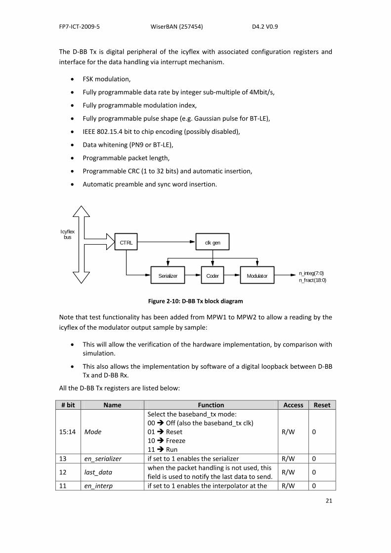
The D-BB Tx is digital peripheral of the icyflex with associated configuration registers and
interface for the data handling via interrupt mechanism.
FSK modulation,
Fully programmable data rate by integer sub-multiple of 4Mbit/s,
Fully programmable modulation index,
Fully programmable pulse shape (e.g. Gaussian pulse for BT-LE),
IEEE 802.15.4 bit to chip encoding (possibly disabled),
Data whitening (PN9 or BT-LE),
Programmable packet length,
Programmable CRC (1 to 32 bits) and automatic insertion,
Automatic preamble and sync word insertion.
CTRL clk gen
CoderSerializer Modulator
Icyflexbus
n_integ(7:0)
n_fract(18:0)
Figure 2-10: D-BB Tx block diagram
Note that test functionality has been added from MPW1 to MPW2 to allow a reading by the
icyflex of the modulator output sample by sample:
This will allow the verification of the hardware implementation, by comparison with simulation.
This also allows the implementation by software of a digital loopback between D-BB Tx and D-BB Rx.
All the D-BB Tx registers are listed below:
# bit Name Function Access Reset
15:14 Mode
Select the baseband_tx mode: 00 Off (also the baseband_tx clk) 01 Reset 10 Freeze 11 Run
R/W 0
13 en_serializer if set to 1 enables the serializer R/W 0
12 last_data when the packet handling is not used, this field is used to notify the last data to send.
R/W 0
11 en_interp if set to 1 enables the interpolator at the R/W 0
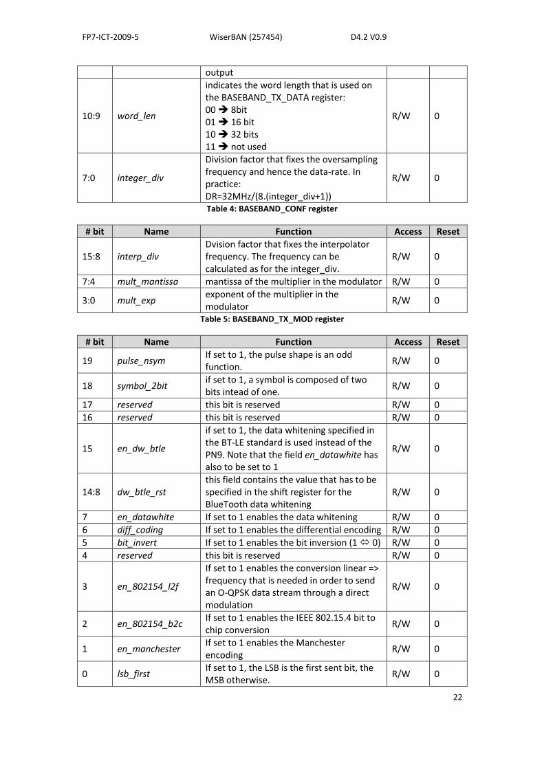
FP7-ICT-2009-5 WiserBAN (257454) D4.2 V0.9
22
output
10:9 word_len
indicates the word length that is used on the BASEBAND_TX_DATA register: 00 8bit 01 16 bit 10 32 bits 11 not used
R/W 0
7:0 integer_div
Division factor that fixes the oversampling frequency and hence the data-rate. In practice: DR=32MHz/(8.(integer_div+1))
R/W 0
Table 4: BASEBAND_CONF register
# bit Name Function Access Reset
15:8 interp_div Dvision factor that fixes the interpolator frequency. The frequency can be calculated as for the integer_div.
R/W 0
7:4 mult_mantissa mantissa of the multiplier in the modulator R/W 0
3:0 mult_exp exponent of the multiplier in the modulator
R/W 0
Table 5: BASEBAND_TX_MOD register
# bit Name Function Access Reset
19 pulse_nsym If set to 1, the pulse shape is an odd function.
R/W 0
18 symbol_2bit if set to 1, a symbol is composed of two bits intead of one.
R/W 0
17 reserved this bit is reserved R/W 0
16 reserved this bit is reserved R/W 0
15 en_dw_btle
if set to 1, the data whitening specified in the BT-LE standard is used instead of the PN9. Note that the field en_datawhite has also to be set to 1
R/W 0
14:8 dw_btle_rst this field contains the value that has to be specified in the shift register for the BlueTooth data whitening
R/W 0
7 en_datawhite If set to 1 enables the data whitening R/W 0
6 diff_coding If set to 1 enables the differential encoding R/W 0
5 bit_invert If set to 1 enables the bit inversion (1 0) R/W 0
4 reserved this bit is reserved R/W 0
3 en_802154_l2f
If set to 1 enables the conversion linear => frequency that is needed in order to send an O-QPSK data stream through a direct modulation
R/W 0
2 en_802154_b2c If set to 1 enables the IEEE 802.15.4 bit to chip conversion
R/W 0
1 en_manchester If set to 1 enables the Manchester encoding
R/W 0
0 lsb_first If set to 1, the LSB is the first sent bit, the MSB otherwise.
R/W 0

FP7-ICT-2009-5 WiserBAN (257454) D4.2 V0.9
23
Table 6: BASEBAND_CODING register
# bit Name Function Access Reset
7 en_crc If set to 1 enables the CRC calculation and automatic insertion
R/W 0
6:5 pattern_word_len
Set the pattern word length. 00 8bit 01 16 bit 10 32 bits 11 not used
R/W 0
4 en_multiframe If set to 1 enables the multi-frame mode (experimental)
R/W 0
3 en_address If set to 1 enables the automatic address insertion
R/W 0
2 en_preamble If set to 1 enables the automatic preamble insertion
R/W 0
1 en_packet_len_fix If set to 1, the packet will have a fixed length. The length can be written in the BASEBAND_PKT_LEN register.
R/W 0
0 en_packet If set to 1, enables the packet handler R/W 0 Table 7: BASEBAND_PKT_HDL register
# bit Name Function Access Reset
13:10 correction Signed value that specifies the correction to be added to the packet length
R/W 0
9:8 position unsigned value that specifies the position of the packet length inside the payload.
R/W 0
7:0 length Unsigned value that specifies the length of the packet in case of a fix packet length protocol.
R/W 0
Table 8: BASEBAND_PKT_LEN register
# bit Name Function Access Reset
31:0 pattern Pattern to be send (sync word) R/W 0 Table 9: BASEBAND_PATTERN register
# bit Name Function Access Reset
31:0 crc_polynomial
CRC polynomial. It is coded using the Koopman notation, i.e. the nth bit codes the (n+1) coefficient. Example: x16+x12+x5+1 0x8810.
R/W 0
Table 10: BASEBAND_CRC_POLY register
# bit Name Function Access Reset
31:0 crc_rst Reset value of the CRC R/W 0 Table 11: BASEBAND_CRC_RST register
# bit Name Function Access Reset
26:0 mod_cfreq Central frequency. R/W 0 Table 12: BASEBAND_MOD_CFREQ register
FP7-ICT-2009-5 WiserBAN (257454) D4.2 V0.9
24
# bit Name Function Access Reset
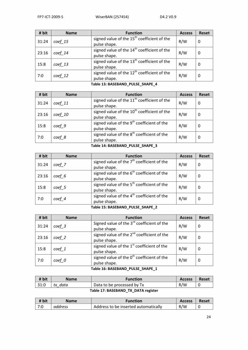
31:24 coef_15 signed value of the 15th coefficient of the pulse shape.
R/W 0
23:16 coef_14 signed value of the 14th coefficient of the pulse shape.
R/W 0
15:8 coef_13 signed value of the 13th coefficient of the pulse shape.
R/W 0
7:0 coef_12 signed value of the 12th coefficient of the pulse shape.
R/W 0
Table 13: BASEBAND_PULSE_SHAPE_4
# bit Name Function Access Reset
31:24 coef_11 signed value of the 11th coefficient of the pulse shape.
R/W 0
23:16 coef_10 signed value of the 10th coefficient of the pulse shape.
R/W 0
15:8 coef_9 signed value of the 9th coefficient of the pulse shape.
R/W 0
7:0 coef_8 signed value of the 8th coefficient of the pulse shape.
R/W 0
Table 14: BASEBAND_PULSE_SHAPE_3
# bit Name Function Access Reset
31:24 coef_7 signed value of the 7th coefficient of the pulse shape.
R/W 0
23:16 coef_6 signed value of the 6th coefficient of the pulse shape.
R/W 0
15:8 coef_5 signed value of the 5th coefficient of the pulse shape.
R/W 0
7:0 coef_4 signed value of the 4th coefficient of the pulse shape.
R/W 0
Table 15: BASEBAND_PULSE_SHAPE_2
# bit Name Function Access Reset
31:24 coef_3 Signed value of the 3rd coefficient of the pulse shape.
R/W 0
23:16 coef_2 signed value of the 2nd coefficient of the pulse shape.
R/W 0
15:8 coef_1 signed value of the 1st coefficient of the pulse shape.
R/W 0
7:0 coef_0 signed value of the 0th coefficient of the pulse shape.
R/W 0
Table 16: BASEBAND_PULSE_SHAPE_1
# bit Name Function Access Reset
31:0 tx_data Data to be processed by Tx R/W 0 Table 17: BASEBAND_TX_DATA register
# bit Name Function Access Reset
7:0 address Address to be inserted automatically R/W 0
FP7-ICT-2009-5 WiserBAN (257454) D4.2 V0.9
25
Table 18: BASEBAND_ADDRESS register
# bit Name Function Access Reset
7:0 preamble Preamble to be inserted automatically R/W 0 Table 19: BASEBAND_PREAMBLE register
# bit Name Function Access Reset
7:0 preamble_len Length of the preamble -1. R/W 0 Table 20: BASEBAND_PREAMBLE_LEN register
2.4 D-BB TX test methodology and validation
The D-BB Tx has been benched by digital simulation, with the targeted modulations, with a
corresponding D-BB Rx different from the one described in the preceding Section 2.1 and
2.2.
This D-BB Tx has been integrated into the MPW1 SoC. The more interesting validation is then
realized by measurement of the modulated output of the SoC, at RF level, for the different
targeted modulations.
In addition to the below measurements of continuous transmissions, it would have been
also interesting to validate the different frame formats at RF level. This can only be
performed by the use of corresponding demodulator with RF input, the more interesting
configuration being the use of the Rx analogue chain and demodulator that will be
integrated in the SoC.
If we consider that the proprietary modulation is equivalent to IEEE802.15.4-2006
modulation without the spreading, both modulation spectrums and eyes correspond to a
2Mbit/s MSK. The below Figure 2-11 displays the output spectrum and eye diagram for
continuous 2Mbit/s MSK modulation that corresponds to the BT-LE modulation: the output
spectrum is very close to the output spectrum of a generator configured for the same
modulation and the eye is widely opened. The close spectrum as well as parasitic spurs are
well below the IEEE802.15.4-2006 standard mask.

FP7-ICT-2009-5 WiserBAN (257454) D4.2 V0.9
26
Figure 2-11: Output spectrum for MSK 2Mbit/s and associated eye diagram (802.15.4)
The below Figure 2-12 displays the output spectrum and eye diagram for continuous 1Mbit/s
GMSK modulation that corresponds to the BT-LE modulation: the output spectrum is quite
close to the output spectrum of a generator configured for the same modulation and the eye
is widely opened. The close spectrum as well as parasitic spurs are well below the BT-LE
standard mask.
Figure 2-12: Output spectrum for GMSK 1Mbit/s and associated eye diagram (BT-LE)
The validation of the TD-BB Tx at RF level has then been performed but the addition of a
complete loopback with a corresponding receiver would have been desired to validate also
the frame formats at RF level in addition to the digital bench: this need to be performed
before final integration.

FP7-ICT-2009-5 WiserBAN (257454) D4.2 V0.9
27
3 Processor unit validation
3.1 Pre-integration validation
CSEM has been developing SoCs based on the icyflex processor family since several years
already. Those SoCs have been used for the development of numerous applications and
demonstrators. The more important validation is then the verification that the integration of
the icyflex processor and its peripherals in the WiserBAN SoC has been realized properly.
This is performed by running numerous simulations to verify the processor itself and its
digital peripherals. These simulations are implemented with software which is executed by
the processor at the top level of the digital system. As an example, the boot loader software
implanted in the boot ROM has been executed with the top level of the digital system
including the RAM, ROM, digital pads, etc. and even behavioral model of external EEPROM
(provided by EEPROM manufacturer). So the functionality has been verified with good
confidence.
For the implementation into silicon, we verify the results of the synthesis and place & route
tools by running additional verifications prior to the implementation into silicon. These
verifications include back-annotated simulations and use of formal equivalence checking
tools. This gives us a very good level of confidence in the design and has been proven to be
sufficient in practice for numerous circuits in the past.
In order to reduce the effort of the developers in individual projects, CSEM provides low-
level library and program examples. Some of these programs are used for the pre-
integration and post-integration validation of the digital system. They are described in the
following section 3.2.
3.2 Post-integration validation of the functionality
The organization of the software architecture is divided in several layers. A Hardware
Abstraction Layer (HAL) developed by the CEA-Léti hides the detailed control of digital
system, using low-level library and features from the CSEM, and provides to the upper layer
programmer with a simplified hardware-independent interface. This HAL implements
functionality associated to the management of general resources like power consumption,
clock tree, miscellaneous parts used by the peripherals listed in the tables below:
file/folder Comment
Clock Initialization run at startup
DMA Misc. library used to initialize a transfer
Interrupt Used to set the request controller
Mode Layer which helps user to change the system frequency
regops.h Misc. Macro definitions
Runtime low level definitions
sys_timer common timer used by peripherals
wiserbanv1a.h WiserBAN register definitions
Table 21: Digital peripherals HAL functionality

FP7-ICT-2009-5 WiserBAN (257454) D4.2 V0.9
28
Peripheral Short description
gpio0 To configure a GPIO as an input or output or to control/read GPIO pins, user can set any GPIO as interrupt
i2s0 half or full duplex transfer protocol
rtc0 Timers and interruptible calendar based on the low frequency oscillator. Useful for real time operation
spi0 Serial interface, most used on wiserbanv1a PCB, to communicate with the FLASH
spi0_dma Half duplex version of SPI interface, developed to output the clock system divided by 2
Timer Interruptible timer based on the system clock
timer0 Interruptible timer based on the system clock
timer1 Interruptible timer based on the system clock
timer2 Interruptible timer based on the system clock
timer3 Interruptible timer based on the system clock
uart0 Serial interface, used principally as PC gateway Table 22: Digital peripherals HAL functionality
Five operational modes are managed, and described in the Figure 3-1 below:
system_mode_init()Clock init :
Low Frequency oscillator enabled
Osc. calibration
System timer initialized
IRQ initialization
system_set_mode(IDLE)
Run on the BAW:
System clock run at 2MHz
system_set_mode(RUN1)
Run on the BAW:
System clock run at 8MHz
system_set_mode(RUN2)
Run on the BAW:
System clock run at 16MHz
system_set_mode(SLEEP1)
Sleep mode:
Processor sleep;
TIMER
Periph irq
RTC irq
WD irq
GPIO
Available peripherals
IRQ for waking up system
SPI
UART
system_set_mode(RUN3)
Run with the low frequency oscillator:
LF oscillator is calibrated at 32KiHz
I2S
TIMER
GPIO
SPI
UART
I2S
TIMER
GPIO
SPI
UART
I2S
TIMER
GPIO
SPI
Figure 3-1: modes of operation
Specific functionalities like interrupts, clock source selection and test modes that are listed in
the table below have been validated by software:
FP7-ICT-2009-5 WiserBAN (257454) D4.2 V0.9
29
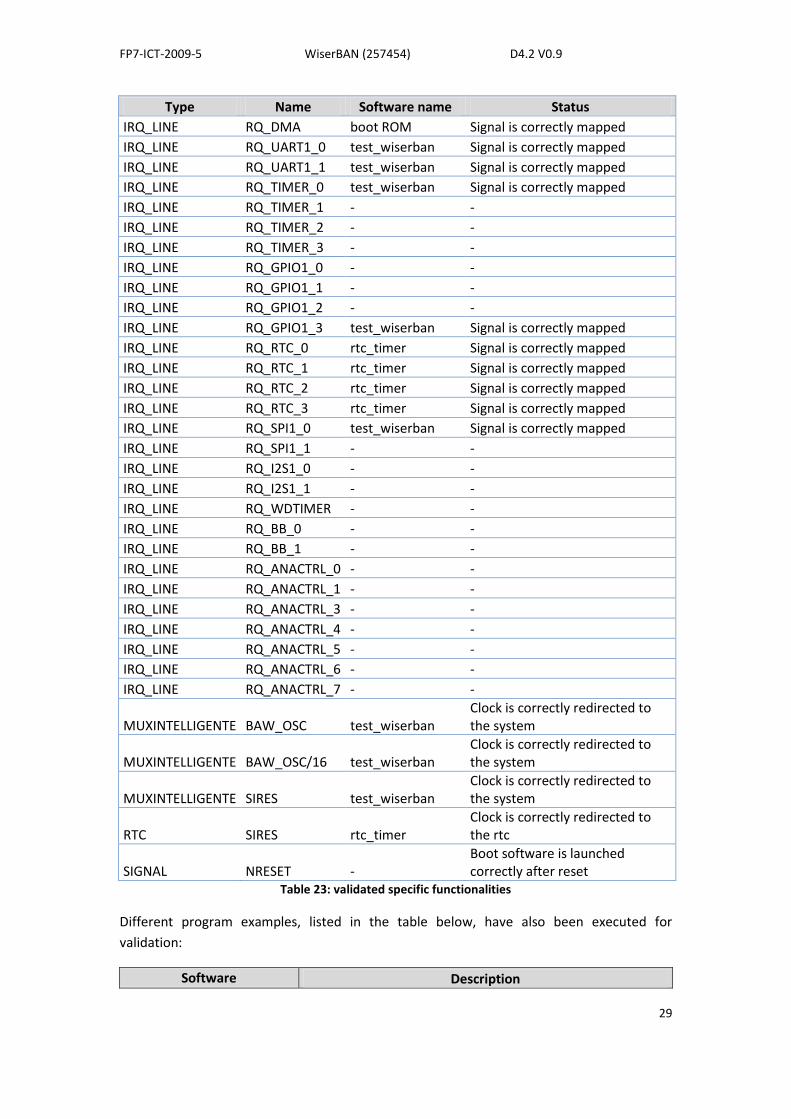
Type Name Software name Status
IRQ_LINE RQ_DMA boot ROM Signal is correctly mapped
IRQ_LINE RQ_UART1_0 test_wiserban Signal is correctly mapped
IRQ_LINE RQ_UART1_1 test_wiserban Signal is correctly mapped
IRQ_LINE RQ_TIMER_0 test_wiserban Signal is correctly mapped
IRQ_LINE RQ_TIMER_1 - -
IRQ_LINE RQ_TIMER_2 - -
IRQ_LINE RQ_TIMER_3 - -
IRQ_LINE RQ_GPIO1_0 - -
IRQ_LINE RQ_GPIO1_1 - -
IRQ_LINE RQ_GPIO1_2 - -
IRQ_LINE RQ_GPIO1_3 test_wiserban Signal is correctly mapped
IRQ_LINE RQ_RTC_0 rtc_timer Signal is correctly mapped
IRQ_LINE RQ_RTC_1 rtc_timer Signal is correctly mapped
IRQ_LINE RQ_RTC_2 rtc_timer Signal is correctly mapped
IRQ_LINE RQ_RTC_3 rtc_timer Signal is correctly mapped
IRQ_LINE RQ_SPI1_0 test_wiserban Signal is correctly mapped
IRQ_LINE RQ_SPI1_1 - -
IRQ_LINE RQ_I2S1_0 - -
IRQ_LINE RQ_I2S1_1 - -
IRQ_LINE RQ_WDTIMER - -
IRQ_LINE RQ_BB_0 - -
IRQ_LINE RQ_BB_1 - -
IRQ_LINE RQ_ANACTRL_0 - -
IRQ_LINE RQ_ANACTRL_1 - -
IRQ_LINE RQ_ANACTRL_3 - -
IRQ_LINE RQ_ANACTRL_4 - -
IRQ_LINE RQ_ANACTRL_5 - -
IRQ_LINE RQ_ANACTRL_6 - -
IRQ_LINE RQ_ANACTRL_7 - -
MUXINTELLIGENTE BAW_OSC test_wiserban Clock is correctly redirected to the system
MUXINTELLIGENTE BAW_OSC/16 test_wiserban Clock is correctly redirected to the system
MUXINTELLIGENTE SIRES test_wiserban Clock is correctly redirected to the system
RTC SIRES rtc_timer Clock is correctly redirected to the rtc
SIGNAL NRESET - Boot software is launched correctly after reset
Table 23: validated specific functionalities
Different program examples, listed in the table below, have also been executed for
validation:
Software Description

FP7-ICT-2009-5 WiserBAN (257454) D4.2 V0.9
30
Example Software provided as model to implement your own application
example2 2nd software provided as model
prog_flash_dmades Used to program the flash memory which is loaded at start-up
rtc_timer An example create to validate the RTC
temp_measure Characterization software
test_wiserban used to validate GPIO, TIMER, SPI, IRQ, UART and components present on the characterisation board
uart0_com used to validate the UART separately Table 24: validation programs
In addition to the functional validation described above, some pass/fail checks have been
performed for different clock frequencies and voltage levels to provide with an indication on
the safety margin associated to the digital integrated in MPW1 run. The pass/fail checks
correspond to the correct execution of the boot loader in ROM that uploads a program in
RAM from the external EEPROM and executes this program that writes a 1kW of data with a
PN16 and reads it back for verification. The results are summarized in the Figure 3-2 below:
Figure 3-2: MPW1 Shmoo plot
The post-integration validations described above are performed with the MPW1 SoC. No
functional issue has been discovered associated to these validations. An indicative safety
margin has been measured. Further functional validation will be performed on-silicon with
MPW2 run before last integration and safety margin need to be conserved.
FP7-ICT-2009-5 WiserBAN (257454) D4.2 V0.9
31
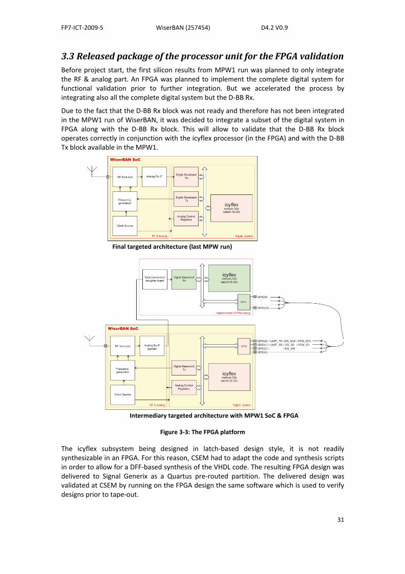
3.3 Released package of the processor unit for the FPGA validation
Before project start, the first silicon results from MPW1 run was planned to only integrate the RF & analog part. An FPGA was planned to implement the complete digital system for functional validation prior to further integration. But we accelerated the process by integrating also all the complete digital system but the D-BB Rx.
Due to the fact that the D-BB Rx block was not ready and therefore has not been integrated in the MPW1 run of WiserBAN, it was decided to integrate a subset of the digital system in FPGA along with the D-BB Rx block. This will allow to validate that the D-BB Rx block operates correctly in conjunction with the icyflex processor (in the FPGA) and with the D-BB Tx block available in the MPW1.
Final targeted architecture (last MPW run)
Intermediary targeted architecture with MPW1 SoC & FPGA
Figure 3-3: The FPGA platform
The icyflex subsystem being designed in latch-based design style, it is not readily synthesizable in an FPGA. For this reason, CSEM had to adapt the code and synthesis scripts in order to allow for a DFF-based synthesis of the VHDL code. The resulting FPGA design was delivered to Signal Generix as a Quartus pre-routed partition. The delivered design was validated at CSEM by running on the FPGA design the same software which is used to verify designs prior to tape-out.
FP7-ICT-2009-5 WiserBAN (257454) D4.2 V0.9
32
4 FPGA implementation
The FPGA implementation is closely linked with mainly tasks “T4.1 Reconfigurable baseband
& MAC” and “T4.3 Low power sensor data processing unit”, but it will also provide with the
infrastructure for testing code developed in task “T4.2 low-power BAN protocol”. It shall
provide a first characterization of the FPGA platform for both testing of SoC VHDL code in
real-time before signing off code for SoC fabrication, as well as running program on the
icyflex DSP core embedded on the FPGA. This dual functionality allows the implementation
risk to be minimized before its fabrication onto silicon.
The FPGA implementation goals within D4.2 are:
Achieve the integration of the icyflex DSP core proprietary functionality, developed by
CSEM, into the FPGA platform and allow the development of icyflex programs
downloaded directly to the FPGA implemented icyflex core and executed.
Achieve the integration of the D-BB Rx, developed by CEA-Léti, into the FPGA
platform and validate its interface with icyflex controller.
Provide with a proof-of-concept for the implementation of the actual MPW1 SoC
receiver datapath functionality, with analog interface, running in real-time on FPGA, if
possible prior to the final SoC fabrication. RF front-end architectures developed in
WP2 can then be tested in this reconfigurable BB with programming functionality.
MAC protocols and user strategies can then be directly tested on an actual hardware
platform and adapted if required.
This section content is organized accordingly.
4.1 General architecture
4.1.1 Hardware Used
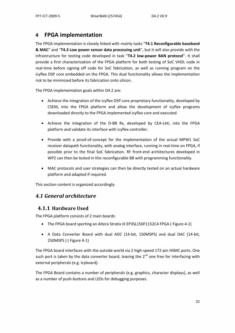
The FPGA platform consists of 2 main boards:
The FPGA board sporting an Altera Stratix III EP3SL150F1152C4 FPGA ( Figure 4-1)
A Data Converter Board with dual ADC (14-bit, 150MSPS) and dual DAC (14-bit,
250MSPS ) ( Figure 4-1)
The FPGA board interfaces with the outside world via 2 high-speed 172-pin HSMC ports. One
such port is taken by the data converter board, leaving the 2nd one free for interfacing with
external peripherals (e.g. Icyboard).
The FPGA Board contains a number of peripherals (e.g. graphics, character displays), as well
as a number of push-buttons and LEDs for debugging purposes.
FP7-ICT-2009-5 WiserBAN (257454) D4.2 V0.9
33
Figure 4-1: The FPGA platform
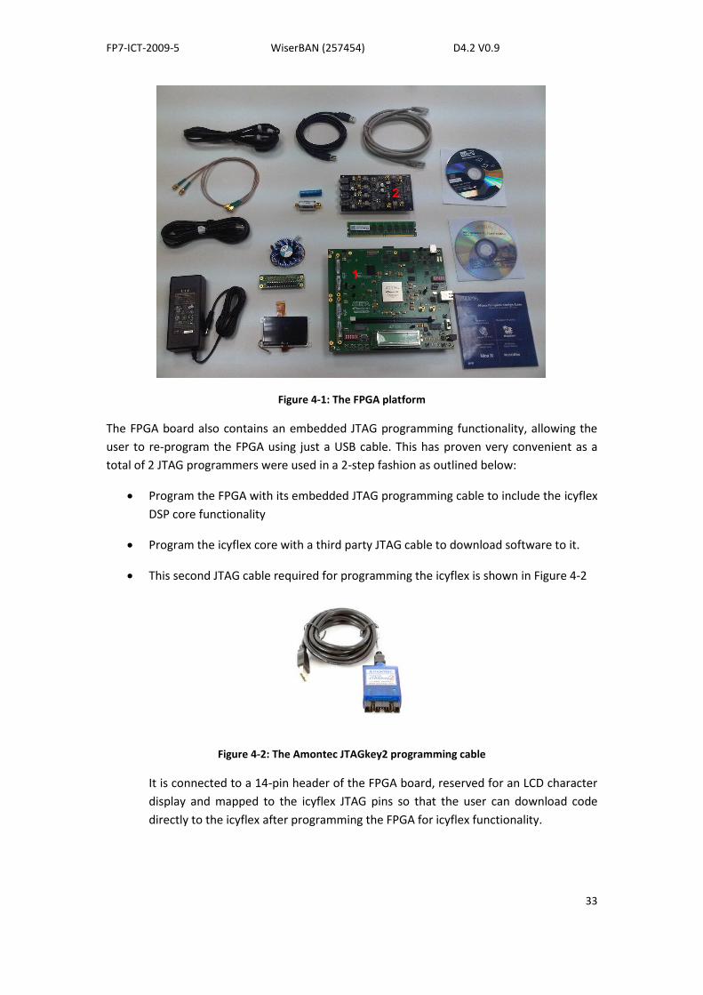
The FPGA board also contains an embedded JTAG programming functionality, allowing the
user to re-program the FPGA using just a USB cable. This has proven very convenient as a
total of 2 JTAG programmers were used in a 2-step fashion as outlined below:
Program the FPGA with its embedded JTAG programming cable to include the icyflex
DSP core functionality
Program the icyflex core with a third party JTAG cable to download software to it.
This second JTAG cable required for programming the icyflex is shown in Figure 4-2
Figure 4-2: The Amontec JTAGkey2 programming cable
It is connected to a 14-pin header of the FPGA board, reserved for an LCD character
display and mapped to the icyflex JTAG pins so that the user can download code
directly to the icyflex after programming the FPGA for icyflex functionality.
FP7-ICT-2009-5 WiserBAN (257454) D4.2 V0.9
34
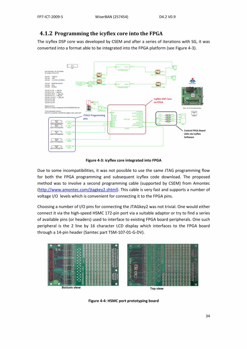
4.1.2 Programming the icyflex core into the FPGA
The icyflex DSP core was developed by CSEM and after a series of iterations with SG, it was
converted into a format able to be integrated into the FPGA platform (see Figure 4-3).
Figure 4-3: icyflex core integrated into FPGA
Due to some incompatibilities, it was not possible to use the same JTAG programming flow
for both the FPGA programming and subsequent icyflex code download. The proposed
method was to involve a second programming cable (supported by CSEM) from Amontec
(http://www.amontec.com/jtagkey2.shtml). This cable is very fast and supports a number of
voltage I/O levels which is convenient for connecting it to the FPGA pins.
Choosing a number of I/O pins for connecting the JTAGkey2 was not trivial. One would either
connect it via the high-speed HSMC 172-pin port via a suitable adaptor or try to find a series
of available pins (or headers) used to interface to existing FPGA board peripherals. One such
peripheral is the 2 line by 16 character LCD display which interfaces to the FPGA board
through a 14-pin header (Samtec part TSM-107-01-G-DV).
Figure 4-4: HSMC port prototyping board
FP7-ICT-2009-5 WiserBAN (257454) D4.2 V0.9
35
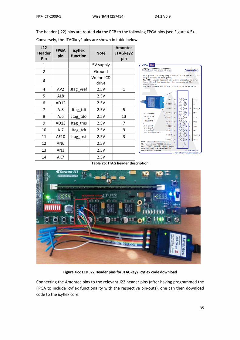
The header (J22) pins are routed via the PCB to the following FPGA pins (see Figure 4-5).
Conversely, the JTAGkey2 pins are shown in table below:
J22 Header
Pin
FPGA pin
icyflex function
Note Amontec JTAGkey2
pin
1 5V supply
2 Ground
3 Vo for LCD
drive
4 AP2 Jtag_vref 2.5V 1
5 AL8 2.5V
6 AD12 2.5V
7 AJ8 Jtag_tdi 2.5V 5
8 AJ6 Jtag_tdo 2.5V 13
9 AD13 Jtag_tms 2.5V 7
10 AJ7 Jtag_tck 2.5V 9
11 AF10 Jtag_trst 2.5V 3
12 AN6 2.5V
13 AN3 2.5V
14 AK7 2.5V
Table 25: JTAG header description
Figure 4-5: LCD J22 Header pins for JTAGkey2 icyflex code download
Connecting the Amontec pins to the relevant J22 header pins (after having programmed the
FPGA to include icyflex functionality with the respective pin-outs), one can then download
code to the icyflex core.
FP7-ICT-2009-5 WiserBAN (257454) D4.2 V0.9
36
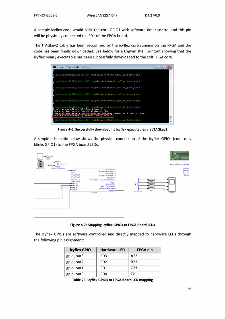
A sample icyflex code would blink the core GPIO1 with software timer control and this pin
will be physically connected to LED1 of the FPGA board.
The JTAGkey2 cable has been recognized by the icyflex core running on the FPGA and the
code has been finally downloaded. See below for a Cygwin shell printout showing that the
icyflex binary executable has been successfully downloaded to the soft FPGA core.
Figure 4-6: Successfully downloading icyflex executables via JTAGkey2
A simple schematic below shows the physical connection of the icyflex GPIOs (code only
blinks GPIO1) to the FPGA board LEDs.
Figure 4-7: Mapping icyflex GPIOs to FPGA Board LEDs
The icyflex GPIOs are software controlled and directly mapped to hardware LEDs through
the following pin assignment:
icyflex GPIO Hardware LED FPGA pin
gpio_out3 LED3 A23
gpio_out2 LED2 B23
gpio_out1 LED1 C23
gpio_out0 LED0 F21
Table 26: icyflex GPIOs to FPGA Board LED mapping
FP7-ICT-2009-5 WiserBAN (257454) D4.2 V0.9
37
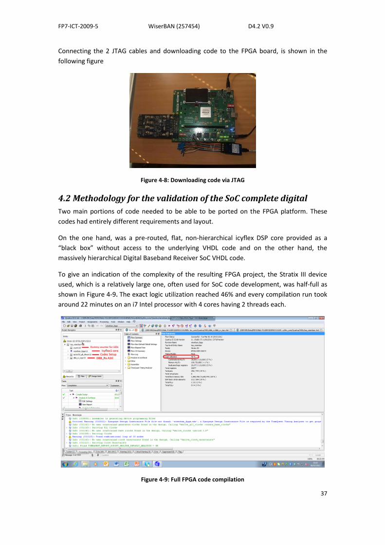
Connecting the 2 JTAG cables and downloading code to the FPGA board, is shown in the
following figure
Figure 4-8: Downloading code via JTAG
4.2 Methodology for the validation of the SoC complete digital
Two main portions of code needed to be able to be ported on the FPGA platform. These
codes had entirely different requirements and layout.
On the one hand, was a pre-routed, flat, non-hierarchical icyflex DSP core provided as a
“black box” without access to the underlying VHDL code and on the other hand, the
massively hierarchical Digital Baseband Receiver SoC VHDL code.
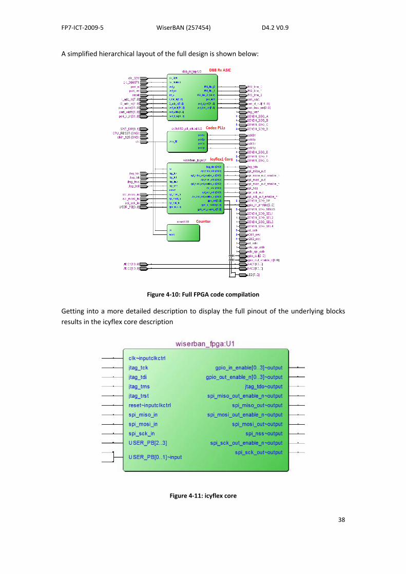
To give an indication of the complexity of the resulting FPGA project, the Stratix III device
used, which is a relatively large one, often used for SoC code development, was half-full as
shown in Figure 4-9. The exact logic utilization reached 46% and every compilation run took
around 22 minutes on an i7 Intel processor with 4 cores having 2 threads each.
Figure 4-9: Full FPGA code compilation
FP7-ICT-2009-5 WiserBAN (257454) D4.2 V0.9
38
A simplified hierarchical layout of the full design is shown below:
Figure 4-10: Full FPGA code compilation
Getting into a more detailed description to display the full pinout of the underlying blocks
results in the icyflex core description
Figure 4-11: icyflex core

FP7-ICT-2009-5 WiserBAN (257454) D4.2 V0.9
39
The D-BB Rx SoC is shown below
Figure 4-12: D-BB Rx SoC
The top level design file, also incorporates all the FPGA board infrastructure components
such as DIP switches, push-buttons, LEDs, seven-segment display etc, so the user can easily
connect subsystem pins to the outside world for debugging.
Furthermore, the dual A/D and D/A converters available via the HSMC Data Converter board
were also mapped and signals to and from the analog domain could enter and exit the FPGA
board. The following Figure shows a loopback operation implemented via the codec board,
where an analog signal from the signal generator is sent to the 1st ADC and then displayed to
the oscilloscope via the 1st DAC.
Figure 4-13: Performing a real time loopback with ADCs and DACs

FP7-ICT-2009-5 WiserBAN (257454) D4.2 V0.9
40
4.3 Results of the FPGA validation
The FPGA validation consisted of two main tasks. Compiling the full D-BB Rx SoC VHDL code
and implementing the icyflex DSP core, both running in parallel. In addition to that, the 14-
bit dual ADCs and DACs were validated by means of a loopback operation and hence the
ADC inputs can now feed signals of varying resolution to the D-BB Rx core. The D-BB Rx core
requires 8-bit ADC inputs for I & Q while the FPGA board ADCs can support up to 14-bit
words. Therefore, some wordlength analysis can also be done in real time by selecting the
more appropriate ADC bits (e.g. [7..0], [8..1] etc) through an AGC (Automated Gain Control)
mechanism. Conversely the D-BB Rx core provides 3 IRQ output lines which can be tied to
LEDs or external logic which can easily be integrated around it. In our simple example a 29-
bit counter was integrated to provide clock divisions from a master clock of 50 MHz down to
about 1 second. It should be noted that the FPGA board has built-in clocks of 50 MHz and
125 MHz (which can be easily used to drive logic), as well as an external clock through an
SMA port (see below) for interfacing with external clocks (e.g. 36.571 MHz).
Figure 4-14: External Input and Output Clocks
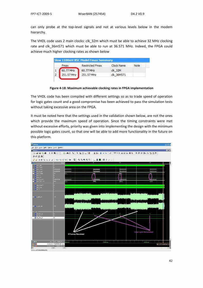
The 7-segment display (shown below) was also integrated in the top-level design file and can
be used to display user feedback.
Figure 4-15: 7-segment display
FP7-ICT-2009-5 WiserBAN (257454) D4.2 V0.9
41
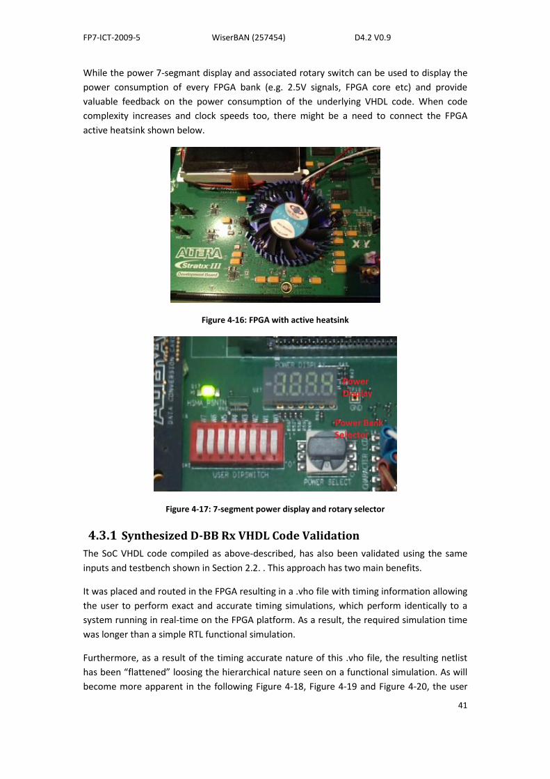
While the power 7-segmant display and associated rotary switch can be used to display the
power consumption of every FPGA bank (e.g. 2.5V signals, FPGA core etc) and provide
valuable feedback on the power consumption of the underlying VHDL code. When code
complexity increases and clock speeds too, there might be a need to connect the FPGA
active heatsink shown below.
Figure 4-16: FPGA with active heatsink
Figure 4-17: 7-segment power display and rotary selector
4.3.1 Synthesized D-BB Rx VHDL Code Validation
The SoC VHDL code compiled as above-described, has also been validated using the same
inputs and testbench shown in Section 2.2. . This approach has two main benefits.
It was placed and routed in the FPGA resulting in a .vho file with timing information allowing
the user to perform exact and accurate timing simulations, which perform identically to a
system running in real-time on the FPGA platform. As a result, the required simulation time
was longer than a simple RTL functional simulation.
Furthermore, as a result of the timing accurate nature of this .vho file, the resulting netlist
has been “flattened” loosing the hierarchical nature seen on a functional simulation. As will
become more apparent in the following Figure 4-18, Figure 4-19 and Figure 4-20, the user
FP7-ICT-2009-5 WiserBAN (257454) D4.2 V0.9
42
can only probe at the top-level signals and not at various levels below in the modem
hierarchy.
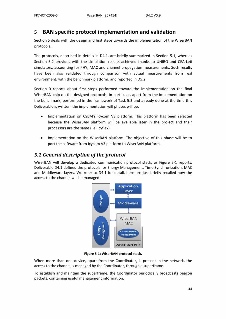
The VHDL code uses 2 main clocks: clk_32m which must be able to achieve 32 MHz clocking
rate and clk_36m571 which must be able to run at 36.571 MHz. Indeed, the FPGA could
achieve much higher clocking rates as shown below
Figure 4-18: Maximum achievable clocking rates in FPGA implementation
The VHDL code has been compiled with different settings so as to trade speed of operation
for logic gates count and a good compromise has been achieved to pass the simulation tests
without taking excessive area on the FPGA.
It must be noted here that the settings used in the validation shown below, are not the ones
which provide the maximum speed of operation. Since the timing constraints were met
without excessive efforts, priority was given into implementing the design with the minimum
possible logic gates count, so that one will be able to add more functionality in the future on
this platform.

FP7-ICT-2009-5 WiserBAN (257454) D4.2 V0.9
43
Figure 4-19: Cycle-accurate simulation of dbb_rx_top showing 3 frames
With a closer look, one can see the address and data decoding taking place where one can
extract the following values:
06 00000005 , 06 00000005 , 06 00000005 , 06 00000005 , 14 5EF3B414 , 14
89B2603F , 14 7A73D029 , etc…
Figure 4-20: Address and Data Decoding
The same testbench, which has been devised by CEA-Léti for the SoC D-BB Rx validation, has
also been used for the FPGA D-BB validation. The VHDL source code was compiled for a
Stratix III FPGA and the resulting timing-accurate file replaced its SoC counterpart. All other
input files, register values, parameters etc… remained identical. The resulting simulation
showed compliance with the expected behavior and this flow can prove itself worthy in
verifying SoC source code prior to manufacturing as well as provide with a more flexible
backup platform in parallel to the SoC validation.
4.3.2 Synthesized icyflex VHDL Code Validation
The icyflex implementation in FPGA has been validated by execution of a downloaded test
program. As the VHDL of D-BB Rx has also been implemented in the FPGA, further validation
of functional assembly of Rx D-BB as peripheral of icyflex will be performed before validation
with analog signals delivered by MPW1.
FP7-ICT-2009-5 WiserBAN (257454) D4.2 V0.9
44
5 BAN specific protocol implementation and validation
Section 5 deals with the design and first steps towards the implementation of the WiserBAN
protocols.
The protocols, described in details in D4.1, are briefly summarized in Section 5.1, whereas
Section 5.2 provides with the simulation results achieved thanks to UNIBO and CEA-Leti
simulators, accounting for PHY, MAC and channel propagation measurements. Such results
have been also validated through comparison with actual measurements from real
environment, with the benchmark platform, and reported in D5.2.
Section 0 reports about first steps performed toward the implementation on the final
WiserBAN chip on the designed protocols. In particular, apart from the implementation on
the benchmark, performed in the framework of Task 5.3 and already done at the time this
Deliverable is written, the implementation will phases will be:
Implementation on CSEM’s Icycom V3 platform. This platform has been selected
because the WiserBAN platform will be available later in the project and their
processors are the same (i.e. icyflex).
Implementation on the WiserBAN platform. The objective of this phase will be to
port the software from Icycom V3 platform to WiserBAN platform.
5.1 General description of the protocol
WiserBAN will develop a dedicated communication protocol stack, as Figure 5-1 reports. Deliverable D4.1 defined the protocols for Energy Management, Time Synchronization, MAC and Middleware layers. We refer to D4.1 for detail, here are just briefly recalled how the access to the channel will be managed.
Figure 5-1: WiserBAN protocol stack.
When more than one device, apart from the Coordinator, is present in the network, the access to the channel is managed by the Coordinator, through a superframe.
To establish and maintain the superframe, the Coordinator periodically broadcasts beacon packets, containing useful management information.
FP7-ICT-2009-5 WiserBAN (257454) D4.2 V0.9
45
The period between two consecutive beacons defines a superframe (SF). The SF will have an active portion and an inactive part; during this latter, nodes can go into a sleeping state in order to reduce the power consumption. The duration of the SF (denoted hereafter as Ts) and of its active part (Ta) should be set depending on the application requirements.
The SF is divided into the following parts (see Figure 5-2):
Beacon portion, reserved for the transmission of the beacon by the Coordinator;
Indicators or poll portion, where nodes have reserved mini-slots to send an acknowledgement (ACK) to the Coordinator in case the beacon has been successfully received;
Contention Free Period (CFP), where the access is TDMA-based: a given number of time slots (TS) is allocated;
Contention Access Period (CAP), where the access to the channel is performed according to a CSMA/CA or a Slotted ALOHA algorithm;
Acknowledgement (ACK) Period, where mini-slots are assigned to the nodes to communicate if the transactions in the SF were successful or not;
Inactive portion, where nodes go to the sleep state.
Figure 5-2: Structure of the proposed superframe.
The duration of the TSs in the CFP will be set such that they could contain the data packet and, in case an ACK is requested, the turn-around-time and the ACK packet.
The CAP should always be present in a SF, at least to handle slot requests. If no other traffic needs to be managed in it, the duration of the CAP will be set to its minimum.
Figure 5-3: SF when different phases are repeated.
Moreover, it is possible to repeat the phases of the SF more than once within the interval between two beacons, if this appears to be useful for some applications (see Figure 5-3). In this way, for example, one can establish a long SF and a node could have more than one time slot allocated in the CFPs with a certain periodicity. This could help handling streaming
FP7-ICT-2009-5 WiserBAN (257454) D4.2 V0.9
46
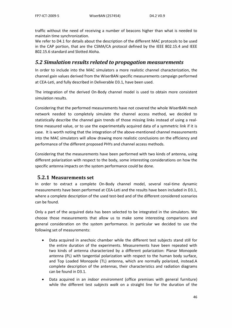
traffic without the need of receiving a number of beacons higher than what is needed to maintain time synchronization. We refer to D4.1 for details about the description of the different MAC protocols to be used in the CAP portion, that are the CSMA/CA protocol defined by the IEEE 802.15.4 and IEEE 802.15.6 standard and Slotted Aloha.
5.2 Simulation results related to propagation measurements
In order to include into the MAC simulators a more realistic channel characterization, the
channel gain values derived from the WiserBAN specific measurements campaign performed
at CEA-Leti, and fully described in Deliverable D3.1, have been used.
The integration of the derived On-Body channel model is used to obtain more consistent
simulation results.
Considering that the performed measurements have not covered the whole WiserBAN mesh
network needed to completely simulate the channel access method, we decided to
statistically describe the channel gain trends of those missing links instead of using a real-
time measured value, or to use the experimentally acquired data of a symmetric link if it is
case. It is worth noting that the integration of the above-mentioned channel measurements
into the MAC simulators will allow drawing more realistic conclusions on the efficiency and
performance of the different proposed PHYs and channel access methods.
Considering that the measurements have been performed with two kinds of antenna, using
different polarization with respect to the body, some interesting considerations on how the
specific antenna impacts on the system performance could be done.
5.2.1 Measurements set In order to extract a complete On-Body channel model, several real-time dynamic
measurements have been performed at CEA-Leti and the results have been included in D3.1,
where a complete description of the used test-bed and of the different considered scenarios
can be found.
Only a part of the acquired data has been selected to be integrated in the simulators. We
choose those measurements that allow us to make some interesting comparisons and
general consideration on the system performance. In particular we decided to use the
following set of measurements:
Data acquired in anechoic chamber while the different test subjects stand still for the entire duration of the experiments. Measurements have been repeated with two kinds of antenna characterized by a different polarization: Planar Monopole antenna (PL) with tangential polarization with respect to the human body surface, and Top Loaded Monopole (TL) antenna, which are normally polarized, instead.A complete description of the antennas, their characteristics and radiation diagrams can be found in D3.1.
Data acquired in an indoor environment (office premises with general furniture) while the different test subjects walk on a straight line for the duration of the

FP7-ICT-2009-5 WiserBAN (257454) D4.2 V0.9
47
acquisitions. Also in this case the measurements have been performed with PL and TL antennas.
We can consider the first set of measurements as a benchmark for the second set, that is to
say that through set a) we are able to evaluate system performance affected only by the
influence on human body, since channel gain values are measured in anechoic chamber
where environment effect is negligible and no movement performed by the subject. On the
contrary, the second set of data refers to a channel that is strongly affected by the specific
environment considered and by the dynamicity of the body.
Finally, note that all the acquisitions have been performed considering the node location
related to the four WiserBAN use-cases as fully described in D1.1.
5.2.2 Simulation settings and scenario
We have performed simulations with the aim of evaluating the performance of the three different contention access schemes proposed for the CAP: i) IEEE 802.15.4 CSMA/CA; ii) IEEE 802.15.6 CSMA/CA; iii) Slotted Aloha.
The cases A and B have been implemented at UNIBO, whereas case C has been implemented at CEA. A common scenario and packet capture model have been considered and implemented in the simulators for fair comparison. Moreover, in both simulators the channel measurements described in the previous section have been included.
The considered reference scenario is the integrated scenario, where four WiserBAN devices are present on the body (see D4.1 for details); we have considered three different sub-scenarios, with different possible positions of the RC, supposed to be held in the left hand (scenario A), to be held in the right hand (scenario B), or to be carried in a pocket (thigh position, scenario C). The three sub-scenarios are reported in Figure 5-5. Therefore results refer to a network composed of four nodes transmitting data to the Coordinator (that is the RC), organized in a star topology and using the CAP portion of the SF as depicted in Figure 5-4.
Figure 5-4: Structure of the superframe considered in the simulator.

FP7-ICT-2009-5 WiserBAN (257454) D4.2 V0.9
48
Figure 5-5: Integrated scenarios for the simulator.
We simulated a simplified traffic, according to which at the beginning of every SF each node has one packet to send, and packets have all the same length. If a node does not succeed in sending its packet before the end of the current SF, the packet is considered as lost. We assume that ACK packets do not collide.
We have simulated 10000 SFs, meaning 10000 packets to be transmitted from each node to the RC.
Performance are evaluated in terms of:
Packet Loss Rate = (Number of packets lost) / (Number of packets generated). Packets can be lost due to connectivity, collisions, or the end of the SF.
Delay: time interval between the beginning of the SF and the correct reception of the node packet at the Coordinator.
Energy consumption: the average energy which is consumed by a node to send its packet in the superframe.
We have considered separately the three different modulation schemes that have been defined at PHY layer:
MSK with spreading PHY (IEEE802.15.4-like), with a bit rate of 250 kbit/s;
MSK without spreading PHY, with a bit rate of 2 Mbit/s;
Bluetooth-LE PHY (GMSK), with a bit rate of 1 Mbit/s.
Packet capture models implemented for the different PHYs will be illustrated in the following subsections, together with the obtained results for the three different access schemes.
In the case of IEEE 802.15.4 CSMA/CA we set {BEmin , BEmax , NBmax}={3,4,5}.
In the case of IEEE 802.15.6 CSMA/CA we set {CWmin, CWmax}={8,16}.
In the case of Slotted Aloha we set {Cpmax, Cpmin}={1/4,1/8}.
Common MAC parameters values set in the simulators are reported in Table 27.

FP7-ICT-2009-5 WiserBAN (257454) D4.2 V0.9
49
Parameter Value
SIFS 50 μs
PHY header + preamble 14 bytes
MAC header + FCS 9 bytes
Beacon length 23 bytes
Ack MPDU length 9 bytes
Maximum number of retransmissions 3
Ack Timeout 2 ms
TB 1 ms
TInd 1 ms
TAck 1 ms
Ta 40 ms
Table 27: MAC simulation parameters
PHY and energy consumption parameters values set in the simulators are reported in Table 28.
Parameter Value
Transmit power 0 dBm
Receiver sensitivity
IEEE 802.15.4 PHY (MSK with
spreading) -96 dBm
MSK without spreading, 2 Mbit/s -87 dBm
Bluetooth-LE PHY (GMSK) -90 dBm
Antenna efficiency, RC -3 dB
Antenna efficiency, nodes -15 dB
Current consumption, transmitting mode 10 mA
Current consumption, receiving mode 10 mA
Current consumption, stand-by (CPU ON) 1.6 mA
Current consumption, stand-by (CPU OFF) 10 A
Supply voltage 1.2 V
Table 28: PHY and energy consumption parameters.
We refer to IR4.2 for details about the packet capture models considered into the simulators
for the different PHYs.
5.2.3 Simulation Results
5.2.3.1 Walking Scenario
The average Packet Loss Rate (PLR) obtained for the walking scenarios, for both the antenna
types, is shown in Figure 5-6 for MSK with spreading PHY.

FP7-ICT-2009-5 WiserBAN (257454) D4.2 V0.9
50
0 20 40 60 80 100 120 140 160 180 20010
-3
10-2
10-1
100
MAC payload [bytes]
PL
R
MSK with spreading (15.4-like) PHY - 250 kbit/sPL antennas, walking scenarios
Scenario A
Scenario B
Scenario C
802.15.6CSMA/CA
802.15.4CSMA/CA
SlottedALOHA
0 20 40 60 80 100 120 140 160 180 20010
-3
10-2
10-1
100
MAC payload [bytes]
PL
R
MSK with spreading (15.4-like) PHY - 250 kbit/sTL antennas, walking scenarios
Scenario A
Scenario B
Scenario C
802.15.4CSMA/CA
802.15.6CSMA/CA
SlottedALOHA
Figure 5-6: PLR obtained for MSK with spreading for PL antenna (left) and TL antenna (right)
A first observation that can be drawn from these figures is that PL antennas lead to worse
PLR performance than TL. This was expected from the measured propagation channel for
the different antennas: PL antennas, in fact, usually produce lower channel gain values (that
means higher attenuation among nodes, causing possible connectivity problems). This
observation will also apply to all results shown hereafter.
The main cause of loss for Slotted Aloha access scheme is the end of SF, especially when the
packet payload is long. This means that the CAP is not correctly dimensioned for this
simulated traffic, where all four devices connected to the network try to transmit their data
at the RC simultaneously. A longer CAP should be allocated, in this case, to decrease the PLR,
taking into account that, on the other hand, this will lead to an increment of the delay. This
case is a good example to show the significance of properly setting the MAC parameters
(e.g., the SF and CAP lengths, the CW value for the Slotted ALOHA, the CSMA/CA parameters
values, etc.).
The average PLR obtained for MSK without spreading PHY (walking scenarios, both types of
antennas) is shown in Figure 5-7.
0 20 40 60 80 100 120 140 160 180 20010
-3
10-2
10-1
100
MAC payload [bytes]
PLR
MSK without spreading PHY - 2 Mbit/sPL antennas, walking scenarios
Scenario A
Scenario B
Scenario C
SlottedALOHA
802.15.4CSMA/CA
802.15.6CSMA/CA
0 20 40 60 80 100 120 140 160 180 20010
-3
10-2
10-1
100
MAC payload [bytes]
PL
R
MSK without spreading PHY - 2 Mbit/sTL antennas, walking scenarios
Scenario A
Scenario B
Scenario C
802.15.4CSMA/CA
SlottedALOHA
802.15.6CSMA/CA
Figure 5-7: PLR obtained for MSK without spreading for PL antenna (left) and TL antenna (right).
For this PHY, the difference between obtained performance with PL and TL is even more
evident than for the MSK with spreading PHY seen above. The PHY under consideration
(MSK without spreading), in fact, has a higher sensitivity value, therefore connectivity issues
are more relevant. When TL antennas are used, the higher bit rate of this PHY (equal to 2
Mbit/s) allows to achieve significantly better PLR than the previously seen PHY, even when
long payload have to be sent.

FP7-ICT-2009-5 WiserBAN (257454) D4.2 V0.9
51
As for the third PHY, BT-LE (GMSK), the average PLR is shown in Figure 5-8. Similar
considerations to those already drawn for the MSK without spreading PHY can be done.
0 20 40 60 80 100 120 140 160 180 20010
-3
10-2
10-1
100
MAC payload [bytes]
PL
R
BT-LE PHY (GMSK) - 1 Mbit/sPL antennas, walking scenarios
Scenario A
Scenario B
Scenario C 802.15.6CSMA/CA
SlottedALOHA
802.15.4CSMA/CA
0 20 40 60 80 100 120 140 160 180 20010
-3
10-2
10-1
100
MAC payload [bytes]
PL
R
BT-LE PHY (GMSK) - 1 Mbit/sTL antennas, walking scenarios
Scenario A
Scenario B
Scenario C
SlottedALOHA
802.15.6CSMA/CA 802.15.4
CSMA/CA
Figure 5-8: PLR obtained for GMSK for PL antenna (left) and TL antenna (right).
Results on the average delay are reported below.
Two main general considerations can be highlighted, which are in line with what seen in the
previous section and in deliverable D4.1:
Performance achieved with PL antennas are worse than the one obtained with TLs;
IEEE 802.15.6 CSMA/CA is the best protocol solution for the delay viewpoint.
0 20 40 60 80 100 120 140 160 180 2000
5
10
15
20
25
30
MAC payload [bytes]
De
lay [m
s]
MSK with spreading (15.4-like) PHY - 250 kbit/sPL antennas, walking scenarios
Scenario A
Scenario B
Scenario C
802.15.6CSMA/CA
SlottedALOHA
802.15.4CSMA/CA
0 20 40 60 80 100 120 140 160 180 2000
5
10
15
20
25
30
MAC payload [bytes]
De
lay [m
s]
MSK with spreading (15.4-like) PHY - 250 kbit/sTL antennas, walking scenarios
Scenario A
Scenario B
Scenario C
SlottedALOHA
802.15.6CSMA/CA
802.15.4CSMA/CA
Figure 5-9: Delay obtained for MSK with spreading for PL antenna (left) and TL antenna (right).
0 20 40 60 80 100 120 140 160 180 2000
5
10
15
20
25
30
MAC payload [bytes]
De
lay [m
s]
MSK without spreading PHY - 2 Mbit/sPL antennas, walking scenarios
Scenario A
Scenario B
Scenario C
802.15.4CSMA/CA
SlottedALOHA
802.15.6CSMA/CA
0 20 40 60 80 100 120 140 160 180 2000
5
10
15
20
25
30
MAC payload [bytes]
De
lay [m
s]
MSK without spreading PHY - 2 Mbit/sTL antennas, walking scenarios
Scenario A
Scenario B
Scenario C
802.15.4CSMA/CA
SlottedALOHA
802.15.6CSMA/CA
Figure 5-10: Delay obtained for MSK without spreading for PL antenna (left) and TL antenna (right).
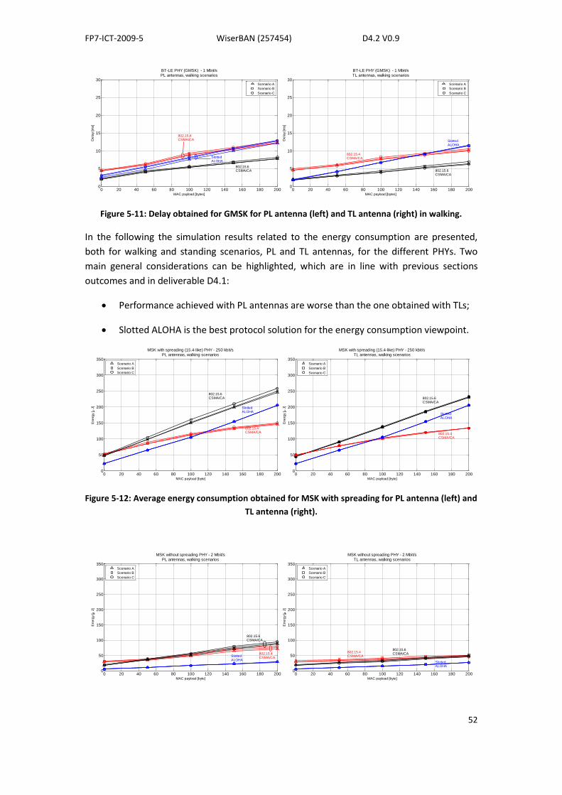
FP7-ICT-2009-5 WiserBAN (257454) D4.2 V0.9
52
0 20 40 60 80 100 120 140 160 180 2000
5
10
15
20
25
30
MAC payload [bytes]
De
lay [m
s]
BT-LE PHY (GMSK) - 1 Mbit/sPL antennas, walking scenarios
Scenario A
Scenario B
Scenario C
802.15.4CSMA/CA
SlottedALOHA
802.15.6CSMA/CA
0 20 40 60 80 100 120 140 160 180 2000
5
10
15
20
25
30
MAC payload [bytes]
De
lay [m
s]
BT-LE PHY (GMSK) - 1 Mbit/sTL antennas, walking scenarios
Scenario A
Scenario B
Scenario C
802.15.4CSMA/CA
SlottedALOHA
802.15.6CSMA/CA
Figure 5-11: Delay obtained for GMSK for PL antenna (left) and TL antenna (right) in walking.
In the following the simulation results related to the energy consumption are presented,
both for walking and standing scenarios, PL and TL antennas, for the different PHYs. Two
main general considerations can be highlighted, which are in line with previous sections
outcomes and in deliverable D4.1:
Performance achieved with PL antennas are worse than the one obtained with TLs;
Slotted ALOHA is the best protocol solution for the energy consumption viewpoint.
0 20 40 60 80 100 120 140 160 180 2000
50
100
150
200
250
300
350
MAC payload [byte]
En
erg
y [
J]
MSK with spreading (15.4-like) PHY - 250 kbit/sPL antennas, walking scenarios
Scenario A
Scenario B
Scenario C
802.15.6CSMA/CA
802.15.4CSMA/CA
SlottedALOHA
0 20 40 60 80 100 120 140 160 180 2000
50
100
150
200
250
300
350
MAC payload [byte]
En
erg
y [
J]
MSK with spreading (15.4-like) PHY - 250 kbit/sTL antennas, walking scenarios
Scenario A
Scenario B
Scenario C
SlottedALOHA
802.15.6CSMA/CA
802.15.4CSMA/CA
Figure 5-12: Average energy consumption obtained for MSK with spreading for PL antenna (left) and
TL antenna (right).
0 20 40 60 80 100 120 140 160 180 2000
50
100
150
200
250
300
350
MAC payload [byte]
En
erg
y [
J]
MSK without spreading PHY - 2 Mbit/sPL antennas, walking scenarios
Scenario A
Scenario B
Scenario C
SlottedALOHA
802.15.6CSMA/CA
802.15.4CSMA/CA
0 20 40 60 80 100 120 140 160 180 2000
50
100
150
200
250
300
350
MAC payload [byte]
En
erg
y [
J]
MSK without spreading PHY - 2 Mbit/sTL antennas, walking scenarios
Scenario A
Scenario B
Scenario C
802.15.4CSMA/CA
802.15.6CSMA/CA
SlottedALOHA
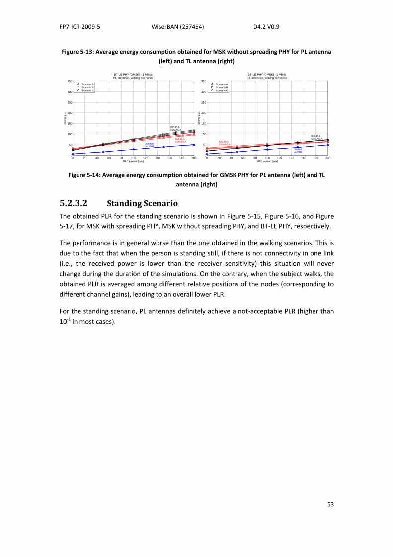
FP7-ICT-2009-5 WiserBAN (257454) D4.2 V0.9
53
Figure 5-13: Average energy consumption obtained for MSK without spreading PHY for PL antenna
(left) and TL antenna (right)
0 20 40 60 80 100 120 140 160 180 2000
50
100
150
200
250
300
350
MAC payload [byte]
En
erg
y [
J]
BT-LE PHY (GMSK) - 1 Mbit/sPL antennas, walking scenarios
Scenario A
Scenario B
Scenario C
802.15.4CSMA/CA
802.15.6CSMA/CA
SlottedALOHA
0 20 40 60 80 100 120 140 160 180 2000
50
100
150
200
250
300
350
MAC payload [byte]
En
erg
y [
J]
BT-LE PHY (GMSK) - 1 Mbit/sTL antennas, walking scenarios
Scenario A
Scenario B
Scenario C
802.15.4CSMA/CA
802.15.6CSMA/CA
SlottedALOHA
Figure 5-14: Average energy consumption obtained for GMSK PHY for PL antenna (left) and TL
antenna (right)
5.2.3.2 Standing Scenario
The obtained PLR for the standing scenario is shown in Figure 5-15, Figure 5-16, and Figure
5-17, for MSK with spreading PHY, MSK without spreading PHY, and BT-LE PHY, respectively.
The performance is in general worse than the one obtained in the walking scenarios. This is
due to the fact that when the person is standing still, if there is not connectivity in one link
(i.e., the received power is lower than the receiver sensitivity) this situation will never
change during the duration of the simulations. On the contrary, when the subject walks, the
obtained PLR is averaged among different relative positions of the nodes (corresponding to
different channel gains), leading to an overall lower PLR.
For the standing scenario, PL antennas definitely achieve a not-acceptable PLR (higher than
10-1 in most cases).
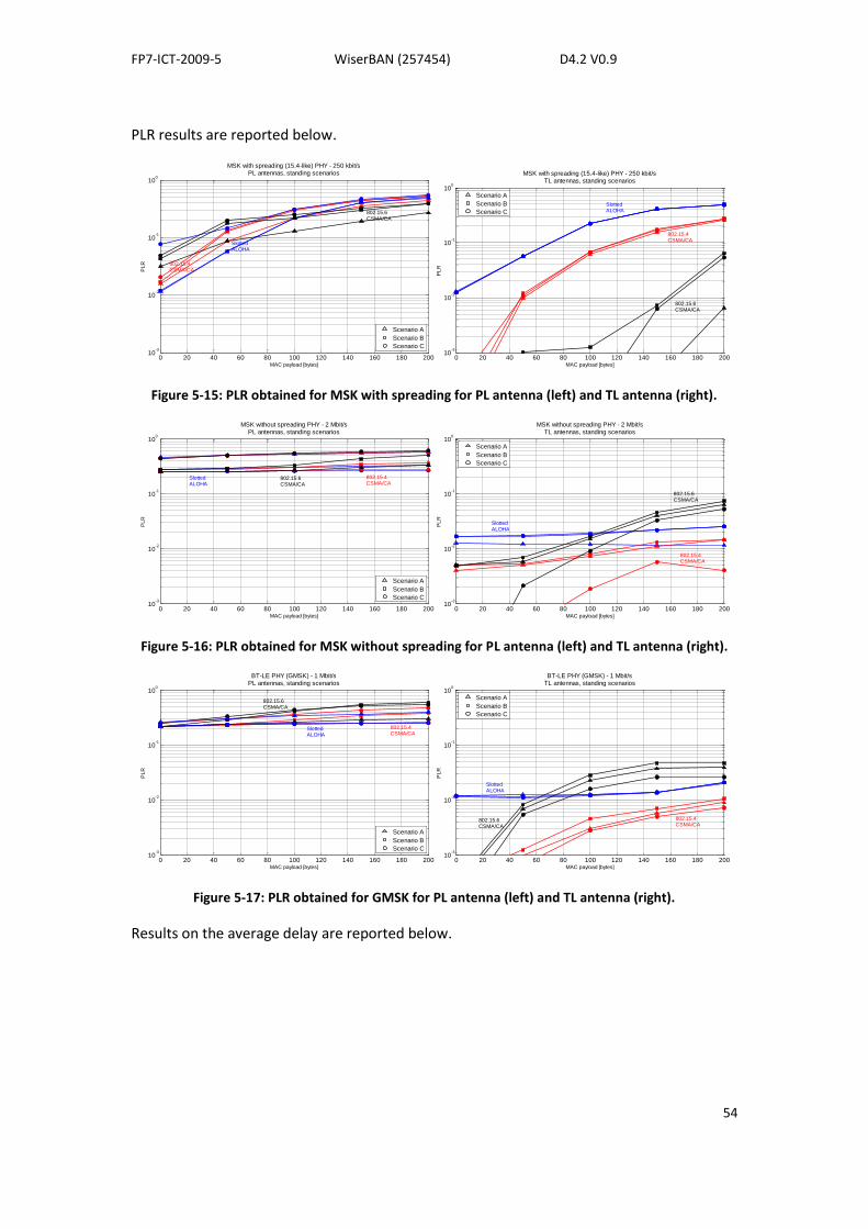
FP7-ICT-2009-5 WiserBAN (257454) D4.2 V0.9
54
PLR results are reported below.
0 20 40 60 80 100 120 140 160 180 20010
-3
10-2
10-1
100
MAC payload [bytes]
PL
R
MSK with spreading (15.4-like) PHY - 250 kbit/sPL antennas, standing scenarios
Scenario A
Scenario B
Scenario C
802.15.4CSMA/CA
802.15.6CSMA/CA
SlottedALOHA
0 20 40 60 80 100 120 140 160 180 20010
-3
10-2
10-1
100
MAC payload [bytes]
PL
R
MSK with spreading (15.4-like) PHY - 250 kbit/sTL antennas, standing scenarios
Scenario A
Scenario B
Scenario C
802.15.6CSMA/CA
802.15.4CSMA/CA
SlottedALOHA
Figure 5-15: PLR obtained for MSK with spreading for PL antenna (left) and TL antenna (right).
0 20 40 60 80 100 120 140 160 180 20010
-3
10-2
10-1
100
MAC payload [bytes]
PL
R
MSK without spreading PHY - 2 Mbit/sPL antennas, standing scenarios
Scenario A
Scenario B
Scenario C
802.15.4CSMA/CA
SlottedALOHA
802.15.6CSMA/CA
0 20 40 60 80 100 120 140 160 180 20010
-3
10-2
10-1
100
MAC payload [bytes]
PL
R
MSK without spreading PHY - 2 Mbit/sTL antennas, standing scenarios
Scenario A
Scenario B
Scenario C
802.15.4CSMA/CA
802.15.6CSMA/CA
SlottedALOHA
Figure 5-16: PLR obtained for MSK without spreading for PL antenna (left) and TL antenna (right).
0 20 40 60 80 100 120 140 160 180 20010
-3
10-2
10-1
100
MAC payload [bytes]
PL
R
BT-LE PHY (GMSK) - 1 Mbit/sPL antennas, standing scenarios
Scenario A
Scenario B
Scenario C
802.15.6CSMA/CA
SlottedALOHA
802.15.4CSMA/CA
0 20 40 60 80 100 120 140 160 180 20010
-3
10-2
10-1
100
MAC payload [bytes]
PL
R
BT-LE PHY (GMSK) - 1 Mbit/sTL antennas, standing scenarios
Scenario A
Scenario B
Scenario C
802.15.4CSMA/CA
SlottedALOHA
802.15.6CSMA/CA
Figure 5-17: PLR obtained for GMSK for PL antenna (left) and TL antenna (right).
Results on the average delay are reported below.
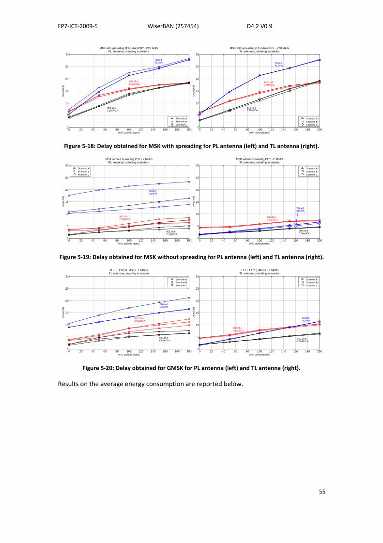
FP7-ICT-2009-5 WiserBAN (257454) D4.2 V0.9
55
0 20 40 60 80 100 120 140 160 180 2000
5
10
15
20
25
30
MAC payload [bytes]
De
lay [m
s]
MSK with spreading (15.4-like) PHY - 250 kbit/sPL antennas, standing scenarios
Scenario A
Scenario B
Scenario C
802.15.6CSMA/CA
802.15.4CSMA/CA
SlottedALOHA
0 20 40 60 80 100 120 140 160 180 2000
5
10
15
20
25
30
MAC payload [bytes]
De
lay [m
s]
MSK with spreading (15.4-like) PHY - 250 kbit/sTL antennas, standing scenarios
Scenario A
Scenario B
Scenario C
802.15.6CSMA/CA
802.15.4CSMA/CA
SlottedALOHA
Figure 5-18: Delay obtained for MSK with spreading for PL antenna (left) and TL antenna (right).
0 20 40 60 80 100 120 140 160 180 2000
5
10
15
20
25
30
MAC payload [bytes]
De
lay [m
s]
MSK without spreading PHY - 2 Mbit/sPL antennas, standing scenarios
Scenario A
Scenario B
Scenario C
SlottedALOHA
802.15.4CSMA/CA
802.15.6CSMA/CA
0 20 40 60 80 100 120 140 160 180 2000
5
10
15
20
25
30
MAC payload [bytes]
De
lay [m
s]
MSK without spreading PHY - 2 Mbit/sTL antennas, standing scenarios
Scenario A
Scenario B
Scenario C
802.15.4CSMA/CA
802.15.6CSMA/CA
SlottedALOHA
Figure 5-19: Delay obtained for MSK without spreading for PL antenna (left) and TL antenna (right).
0 20 40 60 80 100 120 140 160 180 2000
5
10
15
20
25
30
MAC payload [bytes]
De
lay [m
s]
BT-LE PHY (GMSK) - 1 Mbit/sPL antennas, standing scenarios
Scenario A
Scenario B
Scenario C
SlottedALOHA
802.15.4CSMA/CA
802.15.6CSMA/CA
0 20 40 60 80 100 120 140 160 180 2000
5
10
15
20
25
30
MAC payload [bytes]
De
lay [m
s]
BT-LE PHY (GMSK) - 1 Mbit/sTL antennas, standing scenarios
Scenario A
Scenario B
Scenario C
802.15.4CSMA/CA
SlottedALOHA
802.15.6CSMA/CA
Figure 5-20: Delay obtained for GMSK for PL antenna (left) and TL antenna (right).
Results on the average energy consumption are reported below.
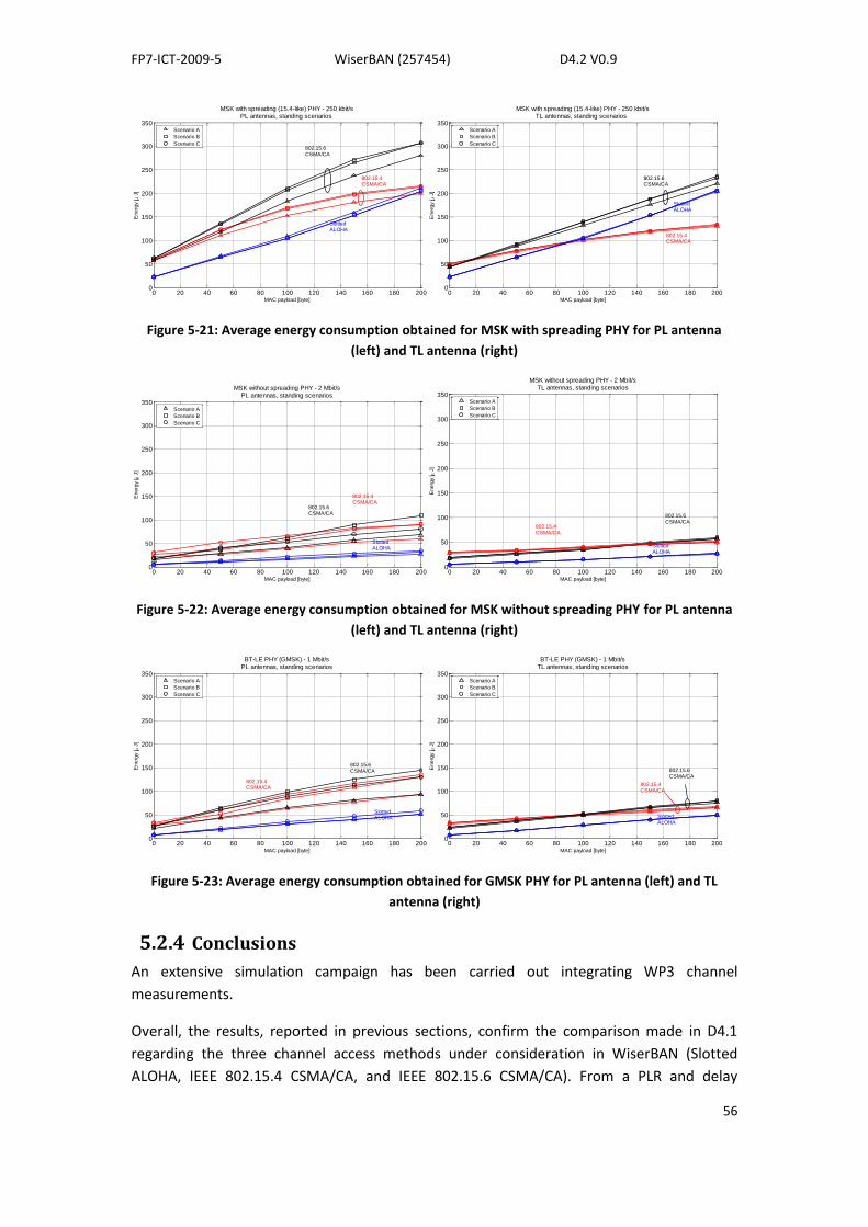
FP7-ICT-2009-5 WiserBAN (257454) D4.2 V0.9
56
0 20 40 60 80 100 120 140 160 180 2000
50
100
150
200
250
300
350
MAC payload [byte]
En
erg
y [
J]
MSK with spreading (15.4-like) PHY - 250 kbit/sPL antennas, standing scenarios
Scenario A
Scenario B
Scenario C802.15.6CSMA/CA
SlottedALOHA
802.15.4CSMA/CA
0 20 40 60 80 100 120 140 160 180 2000
50
100
150
200
250
300
350
MAC payload [byte]
En
erg
y [
J]
MSK with spreading (15.4-like) PHY - 250 kbit/sTL antennas, standing scenarios
Scenario A
Scenario B
Scenario C
SlottedALOHA
802.15.6CSMA/CA
802.15.4CSMA/CA
Figure 5-21: Average energy consumption obtained for MSK with spreading PHY for PL antenna
(left) and TL antenna (right)
0 20 40 60 80 100 120 140 160 180 2000
50
100
150
200
250
300
350
MAC payload [byte]
En
erg
y [
J]
MSK without spreading PHY - 2 Mbit/sPL antennas, standing scenarios
Scenario A
Scenario B
Scenario C
802.15.4CSMA/CA
802.15.6CSMA/CA
SlottedALOHA
0 20 40 60 80 100 120 140 160 180 2000
50
100
150
200
250
300
350
MAC payload [byte]
En
erg
y [
J]
MSK without spreading PHY - 2 Mbit/sTL antennas, standing scenarios
Scenario A
Scenario B
Scenario C
802.15.4CSMA/CA
802.15.6CSMA/CA
SlottedALOHA
Figure 5-22: Average energy consumption obtained for MSK without spreading PHY for PL antenna
(left) and TL antenna (right)
0 20 40 60 80 100 120 140 160 180 2000
50
100
150
200
250
300
350
MAC payload [byte]
En
erg
y [
J]
BT-LE PHY (GMSK) - 1 Mbit/sPL antennas, standing scenarios
Scenario A
Scenario B
Scenario C
802.15.4CSMA/CA
802.15.6CSMA/CA
SlottedALOHA
0 20 40 60 80 100 120 140 160 180 2000
50
100
150
200
250
300
350
MAC payload [byte]
En
erg
y [
J]
BT-LE PHY (GMSK) - 1 Mbit/sTL antennas, standing scenarios
Scenario A
Scenario B
Scenario C
802.15.4CSMA/CA
802.15.6CSMA/CA
SlottedALOHA
Figure 5-23: Average energy consumption obtained for GMSK PHY for PL antenna (left) and TL
antenna (right)
5.2.4 Conclusions
An extensive simulation campaign has been carried out integrating WP3 channel
measurements.
Overall, the results, reported in previous sections, confirm the comparison made in D4.1
regarding the three channel access methods under consideration in WiserBAN (Slotted
ALOHA, IEEE 802.15.4 CSMA/CA, and IEEE 802.15.6 CSMA/CA). From a PLR and delay
FP7-ICT-2009-5 WiserBAN (257454) D4.2 V0.9
57
perspective, both CSMA/CA generally perform better than Slotted ALOHA, while they are on
average more energy consuming. Therefore, all the three protocols will be considered as
possible solution for WiserBAN MAC layer. Due to the huge set of requirements imposed by
different use cases, in fact, one single solution cannot fit all the requirements: the MAC
protocol will be as flexible as possible. Depending on the application requirements the best
solution will be selected case by case, and the simulation results can help the designer in this
choice. To this end, as anticipated in Section 5.1, different application profiles will be defined
and according to such profiles the most appropriate MAC protocol will be selected.
Results also clearly show the impact of the use of different antennas and of the propagation
channel, as for the antenna efficiency. The achieved performance with the PL was always
worse than the one obtained with the TL, as expected. Finally, results show that the
movement of the body improves performance.
Finally, note that some simple aggregation strategy could be implemented to improve
performance. Due to the body movements, in fact, connectivity between couple of nodes
could change frequently. Nodes could store the information data generated when no
connectivity is present and they could transmit the aggregated data when connectivity
comes back. Experimental results addressing this issue are described in D5.2.
5.3 BAN Protocol implementation
5.3.1 The Software Architecture
This section provides an overview of the BAN specific protocol implementation. The key
features of this Medium Access Control (MAC) layer are to interface with other layers and to
support various applications requirements (variable data-rate, quality of service, reliability,
priorities, etc.).
The reference layered system model is given on the figure below.
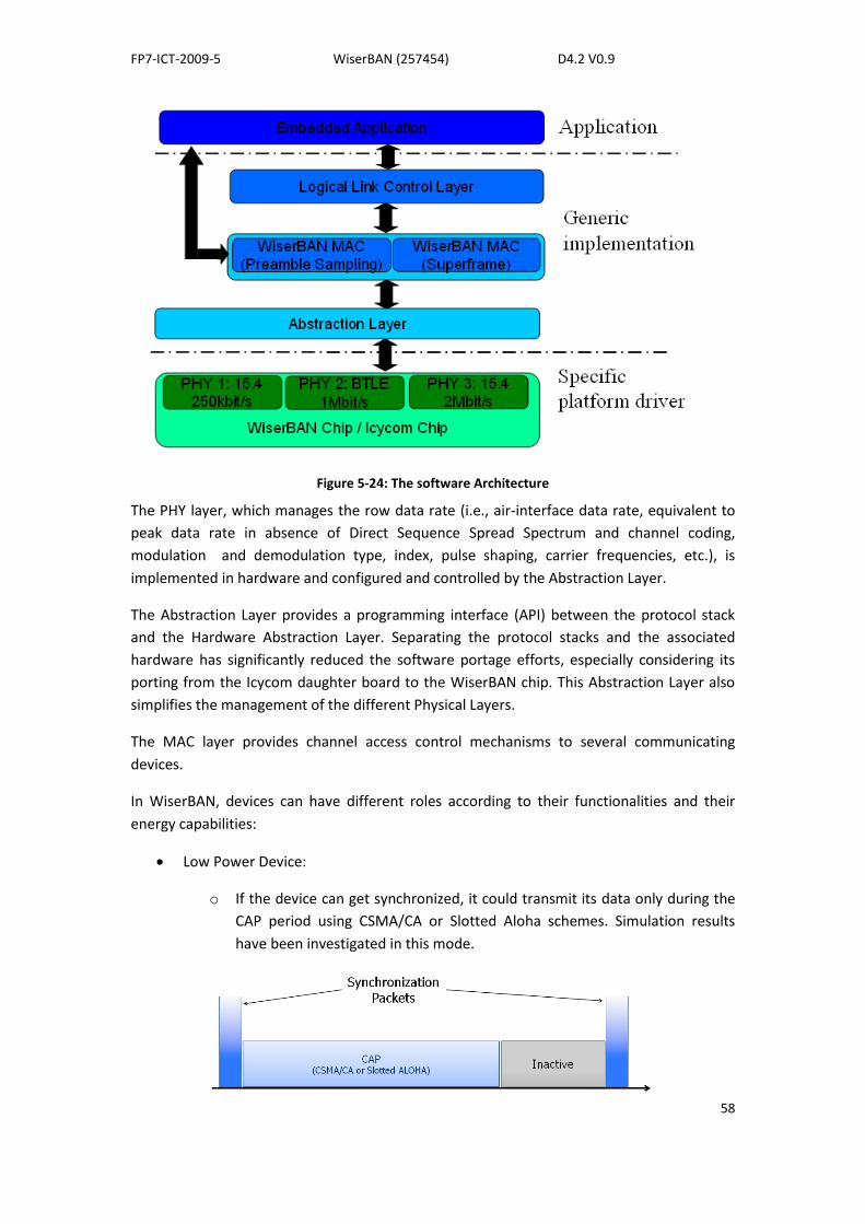
FP7-ICT-2009-5 WiserBAN (257454) D4.2 V0.9
58
Figure 5-24: The software Architecture
The PHY layer, which manages the row data rate (i.e., air-interface data rate, equivalent to
peak data rate in absence of Direct Sequence Spread Spectrum and channel coding,
modulation and demodulation type, index, pulse shaping, carrier frequencies, etc.), is
implemented in hardware and configured and controlled by the Abstraction Layer.
The Abstraction Layer provides a programming interface (API) between the protocol stack
and the Hardware Abstraction Layer. Separating the protocol stacks and the associated
hardware has significantly reduced the software portage efforts, especially considering its
porting from the Icycom daughter board to the WiserBAN chip. This Abstraction Layer also
simplifies the management of the different Physical Layers.
The MAC layer provides channel access control mechanisms to several communicating
devices.
In WiserBAN, devices can have different roles according to their functionalities and their
energy capabilities:
Low Power Device:
o If the device can get synchronized, it could transmit its data only during the
CAP period using CSMA/CA or Slotted Aloha schemes. Simulation results
have been investigated in this mode.

FP7-ICT-2009-5 WiserBAN (257454) D4.2 V0.9
59
Figure 5-25: Low Power Superframe.
o If devices are unsynchronized, preamble sampling should be used.
Reduced Function Device: this mode includes the Low Power Device mode (i.e., the
CAP portion) and the CFP (i.e., nodes can use also TDMA to access the channel).
Devices are associated to the BAN coordinator and the WiserBAN SF is used (Figure
5-2).
Full Function Device: this mode is reserved to high energy capabilities devices which
can potentially manage the coordinator functionalities. The coordinator is in charge
of forming and maintaining the network, maintaining synchronization, and managing
the channel access.
The network could be managed by a device, called WiserBAN Coordinator. The coordinator
will be the Remote control when it is present and it could be substituted by whatever Full
Function Device in case of Remote Control absence.
In WiserBAN project, two MAC schemes are considered: Superframe MAC and Preamble
sampling MAC, also denoted as Low Power Listening (LPL) MAC in the following. In order to
keep a good interoperability of the different proposed MACs, a common MAC state machine
has been defined. This will allow WiserBAN Partners to easily switch between the two
protocols and to define mutual functionalities. Preamble sampling is used when devices
need to save energy and they would like to stay most of the time switched off. At that point
preamble sampling is used to synchronize devices. Once devices are synchronized, if more
than one device is present in the network the superframe is established. Otherwise direct
transmission is used.
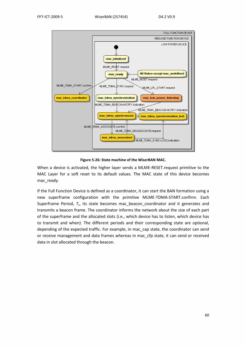
FP7-ICT-2009-5 WiserBAN (257454) D4.2 V0.9
60
Figure 5-26: State machine of the WiserBAN MAC.
When a device is activated, the higher layer sends a MLME-RESET.request primitive to the
MAC Layer for a soft reset to its default values. The MAC state of this device becomes
mac_ready.
If the Full Function Device is defined as a coordinator, it can start the BAN formation using a
new superframe configuration with the primitive MLME-TDMA-START.confirm. Each
Superframe Period, Ts, its state becomes mac_beacon_coordinator and it generates and
transmits a beacon frame. The coordinator informs the network about the size of each part
of the superframe and the allocated slots (i.e., which device has to listen, which device has
to transmit and when). The different periods and their corresponding state are optional,
depending of the expected traffic. For example, in mac_cap state, the coordinator can send
or receive management and data frames whereas in mac_cfp state, it can send or received
data in slot allocated through the beacon.

FP7-ICT-2009-5 WiserBAN (257454) D4.2 V0.9
61
Figure 5-27: Superframe-based MAC State machine.
When the MAC state of a simple device is mac_ready, it can start two different MAC
protocols: Unsynchronized Preamble sampling and Synchronized Superframe schemes.
With the MLME-TDMA-SYNC.request primitive, a simple device can start its synchronization
procedure with the coordinator. This device will seek for a beacon for at most the duration
of a superframe. When it receives a beacon frame, it is considered as synchronized with the
coordinator. Then the MAC layer sends a beacon notification primitive (MLME-BEACON-
NOTIFY.indication) to the next higher layer and its MAC state becomes
mac_tdma_synchronized. The device will have to keep the synchronization by tracking the
beacon with a regular and timely activation of its receiver. If no beacon frame is received
during this time, the number of missed beacons shall be increased by one and the MAC layer
repeats this search. The synchronization is lost if the number of missed beacons reaches
aMaxLostBeacons. Then the MAC layer notifies the higher layer by sending a MLME-SYNC-
LOSS.indication primitive with a loss cause of BEACON_LOSS and its MAC state becomes
mac_tdma_synchronization_lost.
Once the device is synchronized, it can work in two modes depending on its capabilities:
In low power mode according to the low power superframe
In Reduced Function mode after being associated. It can request an association
procedure with the MLME-TDMA-ASSOCIATE.request primitive. The MAC layer
initiates the association procedure, sending an association request command to the
coordinator. If the association request command frame is received correctly, the
MAC layer of the coordinator can accept or refuse the association. An association
response command frame shall be sent to the device so as to confirm or refuse the
association. After that, a MLME-TDMA-ASSOCIATE.confirm primitive is sent to the
higher layer in order to indicate the association has succeeded. Once the device is
associated, it is able to participate to the whole superframe and to request traffic
allocation for transmitting data in the CFP. These requested allocations are granted
by the coordinator.
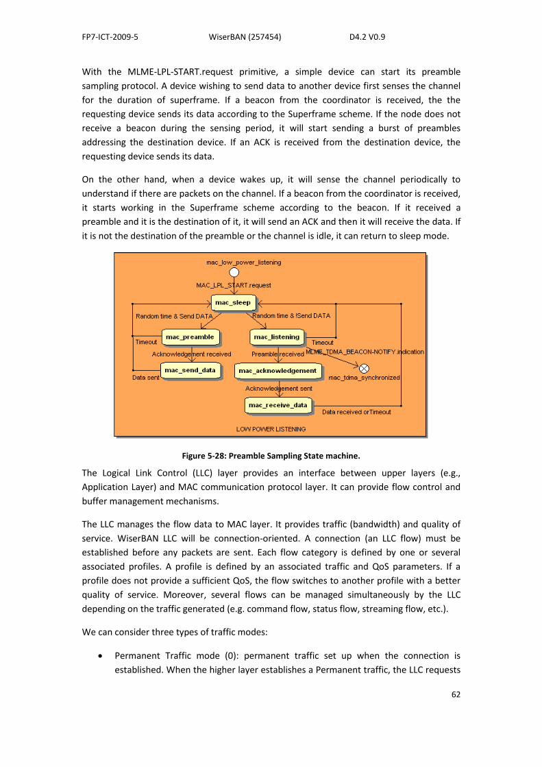
FP7-ICT-2009-5 WiserBAN (257454) D4.2 V0.9
62
With the MLME-LPL-START.request primitive, a simple device can start its preamble
sampling protocol. A device wishing to send data to another device first senses the channel
for the duration of superframe. If a beacon from the coordinator is received, the the
requesting device sends its data according to the Superframe scheme. If the node does not
receive a beacon during the sensing period, it will start sending a burst of preambles
addressing the destination device. If an ACK is received from the destination device, the
requesting device sends its data.
On the other hand, when a device wakes up, it will sense the channel periodically to
understand if there are packets on the channel. If a beacon from the coordinator is received,
it starts working in the Superframe scheme according to the beacon. If it received a
preamble and it is the destination of it, it will send an ACK and then it will receive the data. If
it is not the destination of the preamble or the channel is idle, it can return to sleep mode.
Figure 5-28: Preamble Sampling State machine.
The Logical Link Control (LLC) layer provides an interface between upper layers (e.g.,
Application Layer) and MAC communication protocol layer. It can provide flow control and
buffer management mechanisms.
The LLC manages the flow data to MAC layer. It provides traffic (bandwidth) and quality of
service. WiserBAN LLC will be connection-oriented. A connection (an LLC flow) must be
established before any packets are sent. Each flow category is defined by one or several
associated profiles. A profile is defined by an associated traffic and QoS parameters. If a
profile does not provide a sufficient QoS, the flow switches to another profile with a better
quality of service. Moreover, several flows can be managed simultaneously by the LLC
depending on the traffic generated (e.g. command flow, status flow, streaming flow, etc.).
We can consider three types of traffic modes:
Permanent Traffic mode (0): permanent traffic set up when the connection is
established. When the higher layer establishes a Permanent traffic, the LLC requests

FP7-ICT-2009-5 WiserBAN (257454) D4.2 V0.9
63
one or more slots in the CFP portion of the superframe, according to Packet rate
parameter. When the permanent traffic is established, the application could send
these data. The permanent traffic must be stopped by the higher layer with a
command closing the flow.
Switched Traffic mode (1): Set up and released on demand via a procedure. When
the higher layer establishes a switched traffic, the LLC requests one or more slots in
the CFP for a limited duration when the first data request is received. When the
expected data are sent, the switched traffic is stopped automatically by the LLC.
No Traffic mode (2): Set up for a packet or a set of packets. In this mode, it is not
necessary to establish a traffic and to ask a traffic management to the LLC. This is the
case for a transmission procedure using CAP only or Preamble sampling with direct
transmission.
Several profiles should be defined with the following parameters:
Priority Level: this parameter could permit to a higher flow priority to used
bandwidth to a lower flow priority (e.g. emergency data used bandwidth to
monitoring data).
Traffic mode: this parameter selects the type of traffic used. ( Permanent, Switched
or No traffic mode).
Devices Address.
Packet rate: in some cases, such as monitoring applications, it is necessary to define
the packet rate (i.e., the number of packet per second that the application expect to
send) in order to optimize the MAC protocol.
Acknowledgement policy: several policies could be considered
o 0: No acknowledgement required.
o 1: Immediat Acknowledgment is the same slot or after SIFS.
o 2: Aggregated Acknowledgement in ACK Period.
Transmission and retransmission policy, that is the selected periods for transmission
and retransmission, the number of retransmission allowed.
Maximum Packet Loss Rate tolerable.
Time to Live, which is the time before discarding the data.
Specific flows have to be defined for each WiserBAN scenario with one or two profiles.
When the first profile will not respect the QoS requirements (e.g. loss rate…), the flow will
be able to switch to a second profile (e.g., with a better reliability but a higher power
consumption).
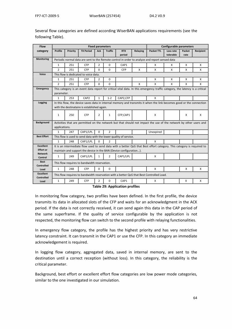
FP7-ICT-2009-5 WiserBAN (257454) D4.2 V0.9
64
Several flow categories are defined according WiserBAN applications requirements (see the
following Table).
Flow
category
Fixed parameters Configurable parameters
Profile Priority TX Period Ack Traffic RTX
period
Relaying Packet TTL Loss rate
tolerable
Packet
rate
Recipient
Monitoring Periodic normal data are sent to the Remote control in order to analyze and report sensed data
1 251 CFP 2 0 CAP1 X X X X
2 251 CFP 0 0 CFP X X X X X
Voice This flow is dedicated to voice data.
1 251 CFP 2 0 X X X X
2 251 CFP 0 0 X X X X X
Emergency This category is an event data report for critical vital data. In this emergency traffic category, the latency is a critical
parameter.
1 253 CAP2 1 1-2 CAP2,CFP X
Logging In this flow, the device saves data in internal memory and transmits it when the link becomes good or the connection
with the destinataire is established again.
1 250 CFP 2 1 CFP,CAP1 X X X
Background Activities that are permitted on the network but that should not impact the use of the network by other users and
applications.
1 247 CAP1/LPL 0 2 Unexpired
Best Effort This flow is used to send data with the lower quality of service.
1 248 CAP1/LPL 0 2 X
Excellent
Effort or
Network
Control
It is an intermediate flow used to send data with a better QoS that Best effort category. This category is required to
maintain and support the device in the BAN (Device configuration…).
1 249 CAP1/LPL 1 2 CAP1/LPL X
Best
Controlled
Load
This flow requires to bandwidth reservation.
1 248 CFP 0 0 X X X
Excellent
Controlled
Load
This flow requires to bandwidth reservation with a better QoS that Best Controlled Load.
1 249 CFP 2 0 CAP1 X X X
Table 29: Application profiles
In monitoring flow category, two profiles have been defined. In the first profile, the device
transmits its data in allocated slots of the CFP and waits for an acknowledgment in the ACK
period. If the data is not correctly received, it can send again this data in the CAP period of
the same superframe. If the quality of service configurable by the application is not
respected, the monitoring flow can switch to the second profile with relaying functionalities.
In emergency flow category, the profile has the highest priority and has very restrictive
latency constraint. It can transmit in the CAP1 or use the CFP. In this category an immediate
acknowledgement is required.
In logging flow category, aggregated data, saved in internal memory, are sent to the
destination until a correct reception (without loss). In this category, the reliability is the
critical parameter.
Background, best effort or excellent effort flow categories are low power mode categories,
similar to the one investigated in our simulation.
FP7-ICT-2009-5 WiserBAN (257454) D4.2 V0.9
65
From applications point of view, MAC and LLC layers will automatically manage the
communication. The application will only set up the parameters according to its
requirements.
A specific flow has to be defined for each WiserBAN scenario with one or several profiles.
When the profile1 does not respect the QoS requirements (e.g. loss rate tolerable) or the
profile use case, the flow can automatically switch to profile2 (e.g. with a better reliability
but an higher power consumption).
According to the scenario specified in D1.1, the different profiles could be used for the
demonstrations.
Monitoring
o This flow could first use an excellent effort flow category (i.e., Preamble
sampling MAC or using CAP in superframe MAC).
o If the QoS requirements are not respected or a superframe MAC is required, this
flow could use:
Excellent control load flow category. The superframe MAC allocates a
bandwidth to this flow. One retransmission is possible in the CAP in case
of failure. Configurable parameters have to be set by the application
layer (i.e., Packet Time-to-Live and packet rate and recipient).
Monitoring flow category. The superframe MAC manages two profiles.
When the profile 1 does not respect the QoS requirements (e.g., loss
rate tolerable), the flow can automatically switch to profile 2 with
relaying capabilities.
Audio Streaming
o This flow could use a best effort flow category (i.e. Preamble sampling MAC)
when the remote control is not present.
o If the QoS requirements are not respected or the remote control is present, this
flow could use:
Best control load flow category. The superframe MAC allocates time
slots into the CPF to this flow.
Voice flow category. The superframe MAC manages two profiles. When
the profile 1 does not respect the QoS requirements (e.g. loss rate
tolerable), the flow can automatically switch to profile 2 with relaying
capabilities. Configurable parameters have to be set by the application
layer (i.e., Packet Time-to-Live, loss rate tolerable, packet rate and
recipient)

FP7-ICT-2009-5 WiserBAN (257454) D4.2 V0.9
66
Volume control, Command or Status
o This flow could use an excellent effort flow category.
Implantation
o This flow could use an emergency traffic.
Data logging
o This flow could use a logging flow category. The device will be able to save its
data in internal memory and to transmit it when the connection is established
again.
5.3.2 The Software Implementation
The implemented software is organized in three different projects.
The first one called icysoft contained all the drivers necessary for an implementation
on the icyflex processor of the Icycom V3 platform. As the processor (i.e. icyflex) is
the same that the one used in the future WiserBAN platform, the first
implementation will be easily reused on the new platform.
Wiserban_csem directory contains usefull information such as WiserBAN platform
drivers. The objective will be to merge from icysoft directory (i.e. Icycom V3
platform) to this directory (i.e. WiserBAN platform).
UniBo and CEA software implementation will be located in directory wiserban_cea
The platform which will be used as first step for the implementation is the Icycom V3
platform, produced by CSEM during Wear-A-BAN European Project. This section describes
the specification of RF Radio transceiver blocks control of the Icycom V3. The RF transceiver
is a communication peripheral that works on a wireless medium.
The RF carrier frequency will be in the range of 863-928MHz for the Icycom V3 whereas for
the WiserBAN platform it will be 2.4-2.5GHz. The Digital Baseband performs the digital
processing part of the RF modulation and demodulation. The icycom V3 modulation is the
MSK modulations with a data rate of 200kbits/s.
The targeted modulation and frame format are the standard Bluetooth Low Energy and
IEEE802.15.4-2006. An additional 2Mbit/s proprietary mode is derived from the
IEEE802.15.4-2006 by removing the spreading coding and decoding. All modes implement
hardware-based CRC.
The WiserBAN radio SoC integrates the 2.45GHz radio transceiver and the controller that
handles the software part of the radio communication protocol. The precise specification is
described in the “IR1.2 Target radio Platform architecture and specifications” document.

FP7-ICT-2009-5 WiserBAN (257454) D4.2 V0.9
67
The selection of the Physical Layer is done with the function radio_init according to the radio
modem:
/**
* @brief Modem of the radio. */
typedef enum {
RADIO_MODEM_DEFAULT, /**< Select the default MODEM */
RADIO_MODEM_IEEE802_15_4, /**< Select the IEEE802.15.4 MODEM */ RADIO_MODEM_BLUETOOTH_LE, /**< Select the Bluetooth low energy MODEM */
RADIO_MODEM_2_MBIT_S_PHY_LAYER /**< Select the 2Mbits/s PHY layer MODEM */
} radio_modem_t;
The header of the radio library implementation and the header to configure the radio are
respectively the files sys_radio.h and radio_configuration.h in the directory
wiserban/icycomv3a/peri/radio/
FP7-ICT-2009-5 WiserBAN (257454) D4.2 V0.9
68
6 Conclusions
The D4.2 goals have been to:
provide with characterization and validation results of the digital blocks which have
been designed in the scope of the implementation into the WiserBAN SoC.
validate the methodology for the validation of the blocks and settle a high level of
confidence in the developed blocks for an expected successful SoC release.
demonstrate the good interoperability of the various blocks designed by the partners
in different places
elaborate and validate by simulation a complete protocol including outcomes from
around-the-body propagation measurements and report about the first steps toward
the implementation.
This deliverable gives a picture of the validation process for the digital implementation on
the WiserBAN module:
First step has been to characterize and derisk the D-BB Rx and Tx process
implementation in order that the SoC can benefit from a high degree of confidence.
This is realized by digital simulation at system level. As soon as possible during the
successive integrations, i.e. when D-BB are available on silicon, this is confirmed by
measurements involving also the RF & analog parts.
The second step has consisted in establishing a link between the simulation and an
actual hardware platform, which can implement into a FPGA the VHDL code
developed for the SoC. This helps to validate by measurement the DBB with loopback
at RF level prior to integration.
Finally, the protocol itself has been presented from its validation point of view by
including the outcomes of the propagation measurements carried out in the WP3 and
integrated into the simulation flow of the whole. In addition, it has been introduced
the preliminary hardware implementation of this protocol onto a platform for real-
time software validation.
If validation has not been completed because of not yet finished SoC design, at the time of
writing this document, the validation process has been entirely defined and already been
followed for an important part of the final target: in summary, measurement of integrated
D-BB Tx, in-depth simulation of designed D-BB Rx and its associated testbench, simulation of
protocol, realization and validation of hardware platforms for future hardware-based
validation of complete D-BB and protocol prior to final integration.
FP7-ICT-2009-5 WiserBAN (257454) D4.2 V0.9
69
7 Annexes
7.1 List of Tables
Table 1: D-BB Rx registers........................................................................................................ 12
Table 2: Functional tests carried out on the D-BB Rx .............................................................. 15
Table 3: Performance tests carried out on the D-BB Rx .......................................................... 20
Table 4: BASEBAND_CONF register ......................................................................................... 22
Table 5: BASEBAND_TX_MOD register .................................................................................... 22
Table 6: BASEBAND_CODING register ..................................................................................... 23
Table 7: BASEBAND_PKT_HDL register ................................................................................... 23
Table 8: BASEBAND_PKT_LEN register .................................................................................... 23
Table 9: BASEBAND_PATTERN register ................................................................................... 23
Table 10: BASEBAND_CRC_POLY register ............................................................................... 23
Table 11: BASEBAND_CRC_RST register .................................................................................. 23
Table 12: BASEBAND_MOD_CFREQ register ........................................................................... 23
Table 13: BASEBAND_PULSE_SHAPE_4 ................................................................................... 24
Table 14: BASEBAND_PULSE_SHAPE_3 ................................................................................... 24
Table 15: BASEBAND_PULSE_SHAPE_2 ................................................................................... 24
Table 16: BASEBAND_PULSE_SHAPE_1 ................................................................................... 24
Table 17: BASEBAND_TX_DATA register ................................................................................. 24
Table 18: BASEBAND_ADDRESS register ................................................................................. 25
Table 19: BASEBAND_PREAMBLE register .............................................................................. 25
Table 20: BASEBAND_PREAMBLE_LEN register ...................................................................... 25
Table 21: Digital peripherals HAL functionality ....................................................................... 27
Table 22: Digital peripherals HAL functionality ....................................................................... 28
Table 23: validated specific functionalities ............................................................................. 29
Table 24: validation programs ................................................................................................. 30
Table 25: JTAG header description .......................................................................................... 35
FP7-ICT-2009-5 WiserBAN (257454) D4.2 V0.9
70
Table 26: icyflex GPIOs to FPGA Board LED mapping .............................................................. 36
Table 27: MAC simulation parameters .................................................................................... 49
Table 28: PHY and energy consumption parameters. ............................................................. 49
Table 29: Application profiles .................................................................................................. 64
7.2 List of Figures
Figure 2-1: Synoptic of the full D-BB including the D-FE and the Modem ................................ 9
Figure 2-2: synoptic of the full-Digital BaseBand .................................................................... 10
Figure 2-3: test bench interface with the D-BB Rx .................................................................. 13
Figure 2-4: frame reception and end_frame IT generation .................................................... 16
Figure 2-5: End_frame activation ( zoom ) .............................................................................. 17
Figure 2-6: Multiple frames reception and generation of fifo_full interrupt .......................... 17
Figure 2-7: Frame reception and fifo_full interrupt generation ( zoom ) ............................... 18
Figure 2-8: Frame reception and generation of a FIFO partial filling interrupt ...................... 18
Figure 2-9: Frame reception and generation of the fifo_part IT ( zoom ) ............................... 19
Figure 2-10: D-BB Tx block diagram ........................................................................................ 21
Figure 2-11: Output spectrum for MSK 2Mbit/s and associated eye diagram (802.15.4) ...... 26
Figure 2-12: Output spectrum for GMSK 1Mbit/s and associated eye diagram (BT-LE) ......... 26
Figure 3-1: modes of operation ............................................................................................... 28
Figure 3-2: MPW1 Shmoo plot ................................................................................................ 30
Figure 3-3: The FPGA platform ................................................................................................ 31
Figure 4-1: The FPGA platform ................................................................................................ 33
Figure 4-2: The Amontec JTAGkey2 programming cable ........................................................ 33
Figure 4-3: icyflex core integrated into FPGA .......................................................................... 34
Figure 4-4: HSMC port prototyping board ............................................................................... 34
Figure 4-5: LCD J22 Header pins for JTAGkey2 icyflex code download ................................... 35
Figure 4-6: Successfully downloading icyflex executables via JTAGkey2 ................................ 36
FP7-ICT-2009-5 WiserBAN (257454) D4.2 V0.9
71
Figure 4-7: Mapping icyflex GPIOs to FPGA Board LEDs ......................................................... 36
Figure 4-8: Downloading code via JTAG .................................................................................. 37
Figure 4-9: Full FPGA code compilation .................................................................................. 37
Figure 4-10: Full FPGA code compilation ................................................................................ 38
Figure 4-11: icyflex core .......................................................................................................... 38
Figure 4-12: D-BB Rx SoC ......................................................................................................... 39
Figure 4-13: Performing a real time loopback with ADCs and DACs ....................................... 39
Figure 4-14: External Input and Output Clocks ....................................................................... 40
Figure 4-15: 7-segment display ............................................................................................... 40
Figure 4-16: FPGA with active heatsink ................................................................................... 41
Figure 4-17: 7-segment power display and rotary selector .................................................... 41
Figure 4-18: Maximum achievable clocking rates in FPGA implementation ........................... 42
Figure 4-19: Cycle-accurate simulation of dbb_rx_top showing 3 frames .............................. 43
Figure 4-20: Address and Data Decoding ................................................................................ 43
Figure 5-1: WiserBAN protocol stack. ..................................................................................... 44
Figure 5-2: Structure of the proposed superframe. ................................................................ 45
Figure 5-3: SF when different phases are repeated. ............................................................... 45
Figure 5-4: Structure of the superframe considered in the simulator. ................................... 47
Figure 5-5: Integrated scenarios for the simulator. ................................................................ 48
Figure 5-6: PLR obtained for MSK with spreading for PL antenna (left) and TL antenna (right)
................................................................................................................................................. 50
Figure 5-7: PLR obtained for MSK without spreading for PL antenna (left) and TL antenna
(right). ...................................................................................................................................... 50
Figure 5-8: PLR obtained for GMSK for PL antenna (left) and TL antenna (right). .................. 51
Figure 5-9: Delay obtained for MSK with spreading for PL antenna (left) and TL antenna
(right). ...................................................................................................................................... 51
Figure 5-10: Delay obtained for MSK without spreading for PL antenna (left) and TL antenna
(right). ...................................................................................................................................... 51
FP7-ICT-2009-5 WiserBAN (257454) D4.2 V0.9
72
Figure 5-11: Delay obtained for GMSK for PL antenna (left) and TL antenna (right) in walking.
................................................................................................................................................. 52
Figure 5-12: Average energy consumption obtained for MSK with spreading for PL antenna
(left) and TL antenna (right). ................................................................................................... 52
Figure 5-13: Average energy consumption obtained for MSK without spreading PHY for PL
antenna (left) and TL antenna (right) ...................................................................................... 53
Figure 5-14: Average energy consumption obtained for GMSK PHY for PL antenna (left) and
TL antenna (right) .................................................................................................................... 53
Figure 5-15: PLR obtained for MSK with spreading for PL antenna (left) and TL antenna
(right). ...................................................................................................................................... 54
Figure 5-16: PLR obtained for MSK without spreading for PL antenna (left) and TL antenna
(right). ...................................................................................................................................... 54
Figure 5-17: PLR obtained for GMSK for PL antenna (left) and TL antenna (right). ................ 54
Figure 5-18: Delay obtained for MSK with spreading for PL antenna (left) and TL antenna
(right). ...................................................................................................................................... 55
Figure 5-19: Delay obtained for MSK without spreading for PL antenna (left) and TL antenna
(right). ...................................................................................................................................... 55
Figure 5-20: Delay obtained for GMSK for PL antenna (left) and TL antenna (right). ............. 55
Figure 5-21: Average energy consumption obtained for MSK with spreading PHY for PL
antenna (left) and TL antenna (right) ...................................................................................... 56
Figure 5-22: Average energy consumption obtained for MSK without spreading PHY for PL
antenna (left) and TL antenna (right) ...................................................................................... 56
Figure 5-23: Average energy consumption obtained for GMSK PHY for PL antenna (left) and
TL antenna (right) .................................................................................................................... 56
Figure 5-24: The software Architecture .................................................................................. 58
Figure 5-25: Low Power Superframe. ...................................................................................... 59
Figure 5-26: State machine of the WiserBAN MAC. ................................................................ 60
Figure 5-27: Superframe-based MAC State machine. ............................................................. 61
Figure 5-28: Preamble Sampling State machine. .................................................................... 62
FP7-ICT-2009-5 WiserBAN (257454) D4.2 V0.9
73
7.3 List of references
[1] Specification of the Bluetooth System, version 4.0, Volume 1 and Volume 6, available at http://www.bluetooth.com, June 2010.
7.4 Abbreviations
ACK Acknowledgment
ACPR Adjacent Channel Power Ratio
ACR Adjacent Channel Rejection
AES Advanced Encryption Standard
AMP Alternate MAC and PHY
ATT Attribute protocol
AWGN Additive White Gaussian Noise
B-ACK Block Acknowledgement
BAN Body Area Network
BAN ID BAN Identifier
BCH Bose, Ray-Chaudhuri, Hocquenghem Code
BER Bit Error Rate
BR Basic Rate
BT-LE BlueTooth Low Energy
CAP Contention Access Phase
CCA Clear Channel Assessment
CCM Cipher Block Chaining-Message Authentication Code
CP Contention Probability
CRC Cyclic Redundancy Check
CSMA/CA Carrier Sense Multiple Access with Collision Avoidance
CW Contention Window
D8PSK Differential 8-Phase-Shift Keying
DBPSK Differential Binary Phase-Shift Keying
DQPSK Differential Quadrature Phase-Shift Keying
EAP Exclusive Access Phase
ED Energy Detection
EDR Enhanced Data Rate
EIRP Equivalent Isotropic Radiated Power
FCS Frame Check Sequence
G-ACK Group Acknowledgement
GAP Generic Access Profile
GATT Generic Attribute protocol
GFSK Gaussian Frequency Shift Keying
GT Guardtime
GTK Group Temporal Key
HBC Human Body Communications
HCI Host Controller Interface
HID Hub Identifier
I-ACK Immediate Acknowledgement
FP7-ICT-2009-5 WiserBAN (257454) D4.2 V0.9
74
ISM Industrial, Scientific and Medical Band
L2CAP Logical Link Control and Adaptation Protocol
L-ACK Block Acknowledgement Later
LE Low Energy
LE ACL LE Asynchronous Connection
LE ADVB LE Advertising Broadcast
LE ADVB-C LE Advertising Broadcast Control Logical Link
LE ADVB-U LE Advertising Broadcast User Data Logical Link
LE-C LE ACL Control Logical Link
LE-U LE User Asynchronous Logical Link
LL Link Layer
LLID Logical Link Identifier
MAC Medium Access Control
MD More Data
MIC Message Integrity Check
MICS Medical Implant Communication System
MK Master Key
MPDU MAC Protocol Data Unit
MPW Multi-Project Wafer (reduced price and number of chips)
MSDU MAC Service Data Unit
N-ACK No Acknowledgement
NESN Next Expected Sequence Number
NID Node Identifier
PDU Protocol Data Unit
PER Packet Error Rate
PHY Physical Layer
PHY SAP PHY Service Access Point
PLCP Physical Layer Convergence Protocol
PLR Packet Loss Rate
PPDU Physical-Layer Protocol Data Unit
PSD Power Spectrum Density
PSDU Physical Layer Service Data Unit
PTK Pairwise Temporal Key
QoS Quality-of-Service
RAP Random Access Phase
RF Radio Frequency
RTT Restricted Tree Topology
SIFS Short Inter-frame Spacing
SMP Security Manager Protocol
SN Sequence Number
SRRC Square-Root Raised Cosine
T-Poll Timed-Poll
UP User Priorities
UWB Ultra Wideband
WMTS Wireless Medical Telemetry System

FP7-ICT-2009-5 WiserBAN (257454) D4.2 V0.9
75