wireless
DESCRIPTION
wirelessTRANSCRIPT

Abstract
Many researchers have speculated on the meaning of the phrase "non-Hertzian waves" as used by Dr. Nikola Tesla. Dr. Tesla first began to use this term in the mid 1890's in order to explain his proposed system for the wireless transmission of electrical power. In fact, it was not until the distinction between the method that Heinrich Hertz was using and the system Dr. Tesla had designed, that Dr. Tesla was able to receive the endorsement of the renowned physicist, Lord Kelvin.1
To this day, however, there
Introduction
A chip for inductive battery charging is presented, which needs no
external components except an antenna to capture the energy from an
electromagnetic field. The integrated system blocks are a front-end to
limit and rectify the induced alternating voltage and a charge regulator
with three control loops for the current, the voltage and the
temperature.
The external antenna forms a resonance circuit with the on-chip
capacitor. The resonance frequency of the front end is 13.56 MHz, so
it is compatible to the well known smart-card standard. In the
electromagnetic field of commercial reader systems the chip produces
an output current to charge a lithium battery with the mandatory
constant-current-constant voltage (cccv) charge profile This
architecture is implemented to charge lithium cells at a current of 4

mA up to a cell voltage of 4.2 volts. The target application are high-
end smart-cards with secondary batteries.
The chip, fabricated in a 0.8 µm BICMOS-technology, includes two
contacts for the antenna and two for the battery. The operating current
of the IC is approximately 1 mA.
Transmitter Block
Voice Signal
User 1
Base Station
Frequency
mixer
V / F Converter
Transmit signal
ElectricSignal OfDC Power Supply

Receiver Block
Receiver signal
Frequency Separator
Voice SignalFor mobile speaker
Frequency Of Electric Signal
Mobile Battery Carger
F / V Converter

CHARGING SYSTEM
Charging profile

Working of project with circuit diagram
In the following sections the different parts of the design are shown with detailed information.They are:
Voltage limiter.
Current & voltage regulation.

Voltage limiter
Integrated circuits work only in a limited voltage range, so special protection circuits are used. For commercial ICs this range is e. g. 4.5V the voltage is regulated by an NMOS transistor, controlled by an amplifier. This transistor regulates the maximum voltage indirectly by shortening the current.
Current & voltage regulation.
Current regulation: The current is measured indirectly by the voltage drop over a small resistor called RSENSE. The voltage drop depends on the current ILOAD and the value of the resistor.
Voltage regulation:
A circuit to limit the output voltage, which is called regulator, is used here. At first, the battery voltage must be divided by an voltage divider which is build of two resistors. This voltage is compared with a stable dc-voltage and the difference is amplified by a loop amplifier
Advantages
Its provide more battery backup
Power theft protection.
It provide emergency power
Less infrastructure cost

Application
Wireless mobile charging
Electrical and Electronic device can charge wireless
We can use in ruler area
Conclusions
An fully integrated inductive charging system was presented in this paper. There are no external components required except the antenna for charging. The charge current for the battery was 4 mA. For the reader and the antenna standard components has been used Implementing this charging system in smart-cards high performance devices with various applications become possible. By the use of rechargeable accumulators, the lifetime of the card is not limited to the capacity of the battery as it was with active cards and primary batteries.

The Wireless Transmission of Electrical Energy Using Schumann Resonance
It has been proven that electrical energy can be propagated around the world between the surface of the Earth and the ionosphere at extreme low frequencies in what is known as the Schumann Cavity. The Schumann cavity surrounds the Earth between ground level and extends upward to a maximum 80 kilometers. Experiments to date have shown that electromagnetic waves of extreme low frequencies in the range of 8 Hz, the fundamental Schumann Resonance frequency, propagate with little attenuation around the planet within the Schumann Cavity.
Knowing that a resonant cavity can be excited and that power can be delivered to that cavity similar to the methods used in microwave ovens for home use, it should be possible to resonate and deliver power via the Schumann Cavity to any point on Earth. This will result in practical wireless transmission of electrical power.
Background
Although it was not until 1954-1959 when experimental measurements were made of the frequency that is propagated in the resonant cavity surrounding the Earth, recent analysis shows that it was Nikola Tesla who, in 1899, first noticed the existence of stationary waves in the Schumann cavity. Tesla's experimental measurements of the wave length and frequency involved closely match Schumann's theoretical calculations. Some of these observations were made in 1899 while Tesla was monitoring the electromagnetic radiations due to lightning discharges in a thunderstorm which passed over his Colorado Springs laboratory and then moved more than 200 miles eastward across the plains. In his Colorado Springs Notes, Tesla noted that these stationary waves "... can be produced with an oscillator," and added in parenthesis, "This is of immense importance."6 The importance of his observations is due to the support they lend to the prime objective of the Colorado Springs laboratory. The intent of the experiments and the

laboratory Tesla had constructed was to prove that wireless transmission of electrical power was possible.
1. HARDWARE DESCRIPTION

RESISTORS: These are current resisting devices.These are made of carbon, metallic
wire wound etc. These are read through this acronym BBROYGBVGW. This stands for,
Black, Brown, Red, Orange, Yellow, Green, Blue, Violet, Gray and, White respectively.
These colors are printed as lines on the resistor the first and second colors lines indicate
the number corresponding to color. The numbers indicated by the colors are shown in
table below. The third line indicate the number of zeros, the fourth line indicate the
percentage of tolerance of the resistor.
BLACK 0 YELLOW 4 GRAY 8
BROWN 1 GREEN 5 WHITE 9
RED 2 BLUE 6 Gold 5%
ORANGE 3 VIOLET 7 Silver 10%
E.g. Red, Red, Black Gold = 22 +/-5%; Red, Red,
Brown = 220 ; Red, Red, Red = 2200; Red, Red, Orange =
22K; Red, Red, Yellow = 220K; Red, Red, Green = 2.2M; Red,
Red, Yellow = 22 M
These are available in various wattages l ike 1/4W, 1/2 W,
1W, 2W, 5W, 10W, 20W, 50W, 100W, 200W. In electronics most
common use are up to 5Watt.Higher the wattages bigger the sizes.
The value and wattage of resisters are to be selected as per the
applications. The tolerance in variat ion of the rated value is also
selected as per the applications. The resisters are fabricated
directly on the IC i tself.
DIODES: These devices allow to f low current in only one
direction. These devices are also called unidirectional devices.
Earlier these devices were made of vacuum tubes, now a days these
are semi conductor solid-state devices. These are PN junction

devices .The PN means doping of the semi conductor with positive
and negative electronic valence atoms. The si l icon diodes have knee
voltage drop of 0.7 volts i.e. forward biased voltage drop whereas
germanium diodes have 0.3 voltage drop. The different diodes are
used for dif ferent purposes. The diodes work in forward biased
condition or reverse biased conditions.
These are available with different current rating, voltage
rating, power rating and are used for different applications. The
diodes of higher wattages are of bigger sizes. The Symbol of Diode
and the ideal curves of diodes are shown below.
Current Voltage Diode Symbol ideal curve
Current
Forward Region
Break Down Voltage
Voltage
Knee Voltage =0.7V
Reverse Region
Diode Characteristics:Diodes are of dif ferent types l ike Photodiode, Varactor
diode, Schotkey Diode, PIN diode, Zener Diode etc.
Zener Diode:

Small signal and rectif ier diodes are never operated in
the break down region because this may damage them. The zener
diode is made to operate in breakdown region, sometimes called
breakdown diode. The zener diode is the back bone of voltage
regulators, circuits that hold the load voltage almost constant
despite large changes in the l ine voltage and load resistance.
Symbol of Zener Diode
Light Emitting Diode:In a forward biased diode, free electrons cross the
junction and fal l in to holes. As these electrons fall from a higher to
a lower energy level, they radiate energy. In ordinary diodes this
energy goes off in the form of heat. But in the l ight emitting diode
(LED) the energy radiates as l ight. LEDs that radiate red, green,
yellow, blue, orange or infrared are manufactured by using elements
like gall ium, arsenic, and phosphorous. LEDs that produce visible
radiations are useful with instruments, calculators etc. The infrared
LED finds application in burglar systems and other areas requiring
invisible radiations. The seven segment displays uses 7 LEDs.
The symbol of LED

TRANSFORMERS: This are the devices which converts the primary ac
voltage to different secondary ac voltages .I f the secondary voltage
is higher then primary voltage then the transformer is called step up transformer , i f the secondary is less then primary voltage then it is
called step down transformer , i f secondary is same as primary
voltage then it is called unity transformer. This unity transformer is
also used as isolation transformer . These devices are highly
efficient unto 99.9%, i.e. very low power loss.
The transformers are required for making dc supply,
tuning circuit etc. The current rating of primary and secondary
winding determines the SWG gauge of the copper wire.
POWER SUPPLIER: The Power is given to the transformer, which steps down
the input voltage to 10 times less i.e. 20 V.
78M05
Transformer Rectifier Filter Regulator
Regulated Power Supply
This low voltage is fed to bridge rectif ier that rectif ies the ac
waveform to dc waveform with some ripples. These ripples are
fi ltered through capacitance fi lter and is fed to l inear regulator .The
output of regulator is further fi ltered to produce clean DC VOLTAGE.
CAPACITORS:

This are the storage devices but has in built Resistance
that’s why the storage voltage does not last for longer period. The
use of capacitor is for tuning the circuit, f i l tering the noise to
ground, creating the t iming pulse as in our case. The capacitors
cannot be fabricated on ICs because of the technical diff iculty.
The different values of capacitor that are available are
1pf, 2pf, 2.2pf, 100pf, 200pf, 1000pf, 0.001uf, and 0.01uf, 0.1uf, 2uf,
10uf, 22uf, 33uf, 47uf, 56uf, 68uf, 82uf, 100uf, 220uf, 330uf etc. The
capacitors are selected based on capacitance and voltage rating.
Higher the voltage higher the size of the capacitor. These are
available in following types.
Electrolytic Capacitor :These capacitors have electrolyte as the dielectric
between the two plates. These are available with polarity + and
-.These are available with vert ical mount or horizontal mount
configuration.
Paper Capacitor :These capacitors are available in low range of
capacitance. The paper is used as dielectrics media between the
two plates.
Mica Capacitor :These capacitors are also available in low range of
capacitance. The mica is used as dielectrics media between the two
plates.
Disc Capacitor : These are available from 1pF to 1ooooUF.
RELAYS:

These are electromagnetic devices which make or
break the contact as per the control voltage. There are solid state
relays which do not consume much power for their operation, but are
not available in higher current rating. Relays are being substituted
by SCRs also called thyrister for on/off control
Relays

INTRODUCTION TO MCS-51 SERISE
Before the era of microprocessor, circuit were
constructed using desecrate logic l ike various gates, counters, f l ip-
flops, decoders, monostables and registers. Circuit diagram was
designed as per the requirement prototype PCB is made
interconnecting the logic components as per the design. Testing
and debugging was done in the lab. During the testing some
modification were required. When the product was tested on the
field, some changes are required this requires new design of PCB.
To overcome this diff icult ies scientist and engineer were
working on a machine, which could read the set of instruction to do
a part icular job called PROGRAM, stored in a memory and executes
it . The instruction would be simple l ike ADD, SUBTRACT, AND, OR,
INVERT, ROTATE and MOVE. If such a machine could made then,
making changes in the design means, making changes in the
program, which is comparatively easy. The birth of computer is also
a result of such thinking. Because of the advancement in the sil icon
technology, i t was possible to design such a device called
microprocessor. The microprocessor wil l read the instruction stored
in Rom, the read only memory, and execute in PROM programmers
were used to put the desired program inside the ROM. This process
called the programming the ROM, also called burning the program
inside the ROM Intel come out f irst with 8080 microprocessor. This
was followed by the 8085, which become vary popular and accepted
by industry al l over the world. The use of 8085, always follows the
use of external ROM like 2764, external RAM 6264, 8bit latch

74LS373, address decoding logic 74LS138, I/O device such as
8155/8255. Serial interface 8251,t imers/counters 8253,or discrete
logic again the effort were made to put al l the standard hardware
logic in one chip. As a result of such an effort, Intel comes out with
MCS-51 series. It has all the above features, i .e. ROM. RAM, I/O,
serial interface. Timers/counters logic built- in chip or embedded in
it . Plus enhanced instruction set. This includes bit manipulation
instruction, and instruction to mult iply and divide 8 bit hexadecimal
number. I t also has code protection features.
When Intel introduced MCS-51 series there were
basically three IC’s in the series, namely 8031,8051 and8751. 8031
needs external ROM like 2764. 8051 has internal but one time
programmable or OTP ROM 8751 has on chip UV erasable ROM
8031 was suitable for production, i t is not possible to reprogram
8751 has UV erasable on chip ROM, which requires 20 minutes to
erase and it was quit expensive. Atmel made a break through and
developed flash version of 8051, called the 89C51 which has built
in Flash Rom .in f lash version applying proper logic levels at
controls pin and just one push at the erase pin can erase program.
The process is called f lash erasing. With this technique exist ing
program can be erased quickly and new program can be burn. The
price of the flash version was also affordable. 89C51 IC’s become
very popular. It is Hardware and Software compatible with MCS-51
series IC 8051.
Quick look at 8085 IC revels that, it has 16 bit for addressing the
memory, which can address 64K memory of which some part can be ROM and
remaining can be RAM. But total of RAM and ROM can not exceed 64K. MCS-51
series can address 64K ROM, 64K RAM & 256 byte internal RAM. Out of the
64K ROM. Not all the ROM resides on the chip 89C59 has 4k of on chip ROM
and rest of the must be physically out side the chip. The 64K RAM is always out
side the chip and is called external RAM. Apart from the 64K external RAM, there

is 256 byte internal RAM which is always in side the chip & is called internal
RAM. Industrial application with moderate complexity can be fitted inside the 4K
of ROM. The 256 byte internal RAM is divided into two equal parts of 128 byte
each. The upper half, from location 128 to 256 is reserved for special purpose
registers & is called SFR area. If program demands extra ROM, one can use
higher version, the 89C52 which has on chip 8K ROM. Next higher version is
also available. Next higher version is also available. The 89C55 has 20K of on
chip ROM. If the program is written in assembly language, 4K ROM of 89C 51 is
more then sufficient for most of the application.
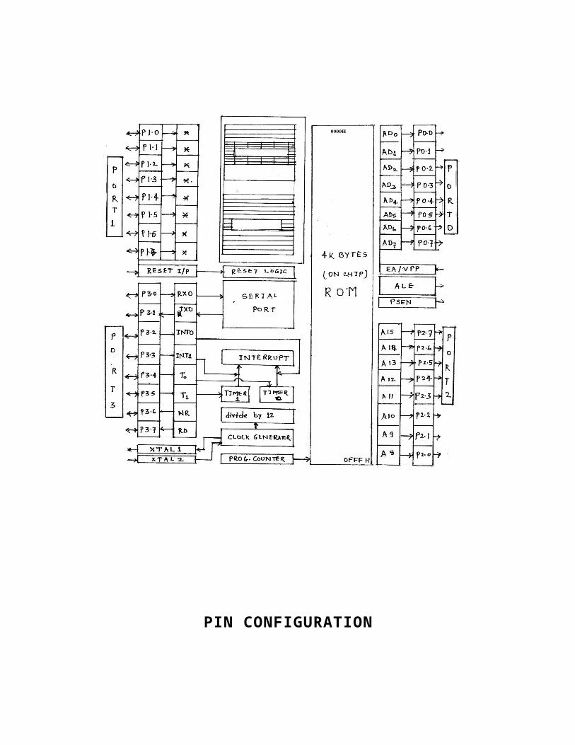
Overview of 89C51

PIN CONFIGURATION
89C51 is a 40 pin device. Two pins are used for power supply,
and require +5V. I t has on chip oscil lator circuitry to which requires

use of external crystal. Normally crystal frequency is around 12MHz.
This oscil lator is further divided by 12 by internally and considered
as clock for machine cycle. Most of the instruction takes one or two
machine cycle to execute. For 12MHz crystal, most of the instruction
wil l get executed in one or two microsecond it has one pin called
ALE. When program execution is going on. ALE pin will pulse at one
sixth of clock frequency. So for 12MHz crystal, ALE pin wil l pulse at
2MHz.it has one pin called Reset. And it requires active high pulse.
Please note that 8085 requires active low reset. After reset program
counter becomes 0000 and program execution starts from 0000. I t
has one pin called PSEN. If external ROM is used then PSEN pin is
connected to RD/ of ROM. So we wil l leave them unconnected in our
design. It has one more pin called EA and has to be connected to
Vcc, so that 89C51 wil l start using internal ROM.
It has four 8 bit ports port 0, port 1, port 2 and port
3. All the ports pin can be used as input or output with out
predefining. Port1, port2 and port3 are internally pulled up through
FET. But port0 requires external pull up resister. After reset all the
port pins are high. Each port has a place in internal RAM and has a
specific address. The address of the port0 is 80 hex, address of the
port1 is 90 hex, address for port2 is A0 hex and address for port3is
B0 hex. Anything that is writ ten to port 0, reading location A0 hex is
same as reading port 2. The port pins are also labeled in dot
notation for convenience. Port 0 pins will labeled as port0.0, port0.1,
port0.2 and so on. Similarly other port pins wil l be labeled.
Fig2 pin configuration

BIT BIT
ADDRESS ADDRESS
90H P1.0 1 40 VCC
91H P1.1 2 P P 39 P0.0 80H
92H P1.2 3 O O 38 P0.1 81H
93H P1.3 4 R(90n) (80n) R 37 P0.2 82H
94H P1.4 5 T T 36 P0.3 83H 95H P1.5 6 35 P0.4 84H 96H P1.6 7 1 0 34 P0.5 85H 97H P1.7 8 33 P0.6 86H RESET 9 32 P0.7 87H B0H P3.0 10 RXD 31 EA/VP VCC B1H P3.1 11 TXD P 30 ALE B2H P3.2 12 INT0 O 29 PSEN RDOF ROY B3H P3.3 13 INT1 R(Bon) 28 P2.7 A7H B4H P3.4 14 T0 T P 27 P2.6 A6H B5H P3.5 15 T1 O 26 P2.3 A5H B6H P3.6 16 WR/ 3(A0n) R 25 P2.4 A4H B7H P3.7 17 RD/ T 24 P2.3 A3H XTL1 18 23 P2.2 A2H XTL2 19 2 22 P2.1 A1H GND 20 21 P2.0 A0H

All the port pins are said to be Bit addressable. The bit addressable
RAM is a new concept. If the RAM location is bit addressable then its in
individual bit has unique bit address. Refer to fig. 2 for pin configuration and bit
addressable concepts. Bits in the bit addressable RAM can be addressed by
their bit address or in the dot notation. The bit address for pin, port 0.0 is 80 hex,
port 0.1 is 81 hex, port 0.2 is 82 hex and so on. The bit address for pin port1.0 is
90 hex, port 1.1 is 91hex,port 1.2 is 92hex and so on. Please note bit address
and port address are different 80 hex bit address means port P0.0 and 80 hex
internal RAM address means port 0 as a complete. There are separate
instruction for addressing bit and byte it is the instruction which decides weather
bit is addressed or byte is addressed 89C51 has instruction to clear the bit ,set
the bit, compliment the bit OR the bit ,AND the bit and conditional jump
instruction depending on , the bit is set or clear.
The pins of the port 3 have alternate use. 89C51 has built in serial
interface two pins are used for this purpose. Serial data will be always received
on port pin P3.0, so the port 3.0 is labeled as RXD and serial data will be
transmitted on port pin P3.1,so the port 3.1 is labeled as TXD. External interrupt
if used will be connected to port pin P3.2 and P3.3. So these pins are labeled as
INT0 and INT1 89C51 has two timer/ counter module they can count pulses
appearing a port pin P3.4 and P3.5 these pins are labeled T0 and T1
respectively
If external ROM or RAM has to be interfaced then port 0 is used as 8
bit multiplexed AD bus. AD0 TO AD7. And port 2 is used as higher order
Addressed Bus A8 to A15. the function of pin ALE is same as in 8085, to
generate strobe for latching lower order address byte. Port pin P3.6 and P6.7 are
connected to WR and RD/ for external RAM.
From the practical point of view, we can say that 89C51 has 4K on
chip Flash ROM and 256 byte of on chip RAM called internal RAM plus it has two
timer/ counter module, serial interface, four 8-bit ports, interrupt handling logic as
standard feature. It can also address 64K external RAM , and /or remaining 60K
of external ROM. But as many as 80 pins are used to interfacing external

memory. As so many pin are lost in interfacing, design using these external
memory are not preferred if one needs more RAM one can use serial EEROM ,
which are more economical, and used 3 lines for interfacing.
89C51 has wonderful features it has multiprocessing mode in this
mode, there is one master 89C51 and no’s of other slave 89C51 master can
communicate with the slave 89C51,sharing the common serial bus, without
disturbing other 89C51 even though they are connected to common serial bus.
This feature is quite advanced. We just mention that chips in the MCS-51 have
multiprocessing capability and is not advised to go into details of it unless person
gathers basic skill in programming.
INTERRUPTS
We have seen earlier that many times, processor has to
respond to event happening real time world. The event may take place at any
time. Interrupts handling logic is incorporated inside the chip, for this purpose. In
such a case, Processor will suspend current execution of the program, & branch
to interrupt service routine. After finishing, it will resume the suspended work.
The situation can be seen very frequently, in our every day life.
Suppose a person is busy in doing some work, say writing a letter and all of a
sudden telephone ring. Then the person will stop writing the book, ans. the
telephone, & resume the writing the book. Some time there are 4,5 telephone
lines are available. In that case he may have to decide about to priority, in
answering the phone. Some times he himself is very busy in imp. meeting,& does
not want to get disturbed by the phone calls. All this types of situations exist in
microprocessor world also.
Those of you who are familiar with 8085 will recall that 8085 can
handle 5 different interrupts. 89C51 can also respond to 5 different interrupting
lines, equivalent of having 5 telephone lines. Two are external interrupts they are
called INT0, INT1 at port pin P3.2 & P3.3 respectively. If these interrupts are
activated & enable in software the program will branch to location 0003 & 0013
hex of program memory (ROM). 89C51 have two timers/counter modules. These
counters are UPCOUNTERS only. When counting starts, during the course of
counting whenever they overflow from FFFF to 0000, timer overflow flag, TF0,
TF1 is set, & interrupts are generated. If the interrupts are enable in software
then the will branch to location 0000bB hex. and 0001B hex respectively. 89C51
has built in serial interface. Whenever serial data is received, Receipt Interrupt
Bit RI is set and whenever data is fully shifted out Transmit
Interrupt bit TI is set. The RI & TI together generate one interrupt, called serial

interrupt. If this interrupt is enabled in software then the program will branch to
location 0023 hex. In ROM memory. The interrupt handling logic of 89C51 can be
explained with the help of following figure -
The external INT0 and INT1 can be defined as either negative edge
triggered or level triggered this means if interrupt is defined as negative edge
triggered interrupt will be generated whenever negative edge is detected on INT0
or INT1 line or if interrupt is defined as level triggered then interrupt is active as
long as INT0 or INT1 is held low. The bits IT0 interrupt type zero and IT1
interrupt type one will decide whether the interrupt is defined as edge triggered
or level triggered. If the byte 0 then corresponding interrupt is level triggered and
if the bit is 1 then it is edge triggered. These bits are found in TCON register in
the SFR area of the internal RAM and its address is 88hex.
EA ----- ET2 ES ET1 EX1 ET0 EX0
Interrupt Enable Register

There is interrupt enable register IE. The bits in the register IE will
decide which interrupts are active or in built. The MSB it of the IE register is the
global enable bit labeled as EA. If this bit is 1 mean interrupt are enabled and if is
0 then all interrupts are disabled. Other bits in the IE register will enable if they
are 1 or disable if they are 0, the individual interrupts. The interrupt enable
register IE has a place in SFR area and its address is A8 hex. It is a bit
addressable register.
There is a provision to decide the priority of the interrupt either
high or low. The priority can be defined in the register IP, interrupt priority register
the address of the register is B8 hex in the SFR area. It is a bit addressable
register if lower priority interrupt work is in progress and higher priority interrupt
arrives. Then lower priority interrupt work will be suspended processor will
branch to higher priority service routine after finishing higher priority work he will
resume the execution lower priority interrupt. And after finishing execution of
lower priority interrupt the procession will go back to start the execution of main
program. If higher priority interrupt is in progress and lower priority interrupt
arrive then lower priority interrupt will be Capt. pending till execution of higher
priority interrupts ends. After finishing higher priority interrupt processor will start
the execution of lower priority interrupt after finishing the same processor will go
back to main program.
----- PT2 PS PT1 PX1 PT0 PX0
Interrupt Priority Register As was mentioned earlier INT0 or INT1 pins will activate the
interrupt in two ways. Interrupt can be defined as edge triggered or level
triggered. IE0 and IE1 or the two bits which actually cases the interrupts. If
interrupts are defined as level triggered then bits IE0 and IE1 will remain set as
long as pins INT0 or INT1 are low. If they are defined as level triggered and
activated then program will branch the respective vector address in ROM and
will start the execution of the service routine. It is then hardwires and /or
programs responsibility to see that pin INT0or INT1 who has cased the interrupt
goes high so that bit IE0 or IE1 will be cleared if INT0or INT1 is not cleared then
program will again enter into the same service routine. Mostly this interrupt are
defined as edge triggered mode only. If they are defined as edge triggered then
the bit IE0 or IE1 will set whenever negative edge is detected and the bits will
automatically get cleared when program branches to respective interrupt service
vector.
Timer over flow bit TF0 or TF1 will set, whenever counter over flow
from FFFF hex to 0000. They will automatically get cleared when program
branches to respective interrupt service vector.
The bits RI and TI in the serial interface logic will be ORed and will
generate one common interrupt. If this interrupt are enabled then program will
start execution at ROM address 0023 hex. These bits will not get cleared
automatically. Program will find out who has cased the interrupt then will take the
appropriate action and program will clear the bit the bits TI and RI are found in
serial control resister SCON. The register SCON is found at address 98hex in the
SFR area.
TIMERS AND COUNTERS
89C51 has 2 on chip, timer/counter modules. They are called
TIMER0 AND TIMER1. They are UP counter only. Both the modules are identical
in nature. Let us consider TIMER0 as shown in the following figure. This figure
will illustrate the working of module clearly.
Diagram
The two register TL0 &TH0 will form 16 bit counter.TL0 & TH0 are
the registers & have place in the SFR area. Their location is 8A hex. & 8C hex.
respectively. They are not bit addressable. The counters are used in UP counter

mode only. While counting UP, whenever it will overflow from FFFF hex. to
0000, the bit TF0 will set. The switch in the small box will pass the pulses to the
counter. Pulses will be passed to counter if out of the AND gate is high. The AND
gate has to input, one is bit TR0 & another is connected to the output of the OR
gate. The OR gate has again 2 input. One is Inverted GATE0 bit &other is
connected to PORT3 Pin P3.2, the INTO. The counter can count the pulses
coming from internal oscillator after division by 12 pulses appearing at Port 3 Pin
P3.4, the T0.The bit C/T0 will decide this.
The bits GATE0, C/T0 of TIMER0 & corresponding bits of TIMER1
the GATE1 & C/T1 are found in register TMOD located at address 89 in the SFR
area. This TMOD register is not bit addressable. The bits TR0, TF0 of TIMER0 &
corresponding bit TR1 & TF1 of TIMER1 are found in the register TCON locate at
address 88 hex. in SFR area. It is a bit addressable register .
When the pulses will be passed to counter, will depending on the
status of bit, GATE0. if the GATE0 bit is cleared i.e. zero then bit TR0 will purely
control the counting. Counting will on as long bit TR0 is SET. So if GATE bit is
zero, then counting will be purely controlled by software. If GATE bit SET, then
counting will be on when Bit TR0 is SET plus port pin P3.2, the INT0 is high.
Thus if GATE bit is zero then counting will be purely controlled by software &if
GATE bit is one then counting will be controlled by software plus hardware.
If we want the bit TF0 to set after counting 2000 pulses. As the
counter is counting up only, we must set registers TH0, TL0, initially to a value
equal to the hexadecimal F830 hex. Which is equivalent of decimal no. 65536 -
2000? So that bit TF0 will set exactly after counting 2000 pluses. If we want the
bit to set regularly after setting 2000 pluses, then we must reload the register
TH0, TL0 to value equal to the hexadecimal equivalent of no. 65536-2000,
WHENEVER THEY BECOME 0000. Usually this is the 1st job of the interrupt
GATE C/T M1 M0 GATE C/T M1 M0 89H TF1 TR1 TF0 TR0 IE1 IT1 IE0 IT0 88H

service routine to reload TH0, TL0. The above mode is called 16 bit counter
mode. This mode is called MODE1.
There is one more mode called MODE2, the 8-Bit Auto Reload
Mode, which is also used very commonly. In this mode counting is done in
register TL0, so it is 8 bit counter mode. After overflow from FF hex. to 00, the
TF0 bit is SET. At the same time data in the register TH1 will be automatically get
copied or reloaded in to register TL0.The register TH0 set to holds the auto
reload count. This will ensure that interrupt will arrive exactly after same time
interval. All other logic will remain same.
The bits M0 & M1 in the TMOD register will set the mode. If both
the bits are 0 then MODE0 is selected. If exactly same as MODE1, except
counting is done 13 bit instead of 16 bit. If the bits are 0 1 then MODE 1, the 16
bit counter mode is selected. This mode we have seen above. If the bits are 1 0
then MODE2, the 8-Bit AUTORELOAD mode is selected. If this bits are 1 then
MODE3, special mode is selected. In this mode TIMER1 is temporally halted.
TL0 & TH0 are used as separate 8 bit counters. Counting logic for TL0 is same
as in case of MODE2. But all control bits of TIMER1 are now diverted for

counting of 8- Bit into TH0. This mode is not used in practice very much because
of the involved complexity.
COMPONENT LIST
SN COMPONENT TYPE QUANTITY1 IC Base 40 PIN 1
2 IC Base 20 PIN 2
3 IC1 89C51 1
4 IC2 & IC3 74245 2
5 Crystal 11.0592 MHz 1
6 Relay 12v D.C. 5
7 Regulator IC 7805 1
8 Regulator IC 7812 1
9 Transistor BC547 5
10 Resistor 10k,1/4W 20
4.7k,1/4W 5
1k,1/4W 1
11 Capacitor 33pf 2
1
7000 microF/25v 1
47 microF/50v 1
100 microF/25v 10
12 LED Red 5
13 Switch Micro 1
14 Diode 1N4007 15

18 Transformer 6-0-6/750mA 1
6-0-6/250mA 1
19 Lead Wire 1
2. CIRCUIT & BLOCK DIAGRAM
CIRCUIT DISCRIPTIONIn microcontroller used is 89C51 whose ports are configured as I/P and output
ports. The pins of input and output ports and both indicator assemble. The ports
P1 is configured as input port and P0 as output port. P1 is from pin 1 and pin8 of
ICR. Pin 18 and 19 are connected to crystal pin 40 and pin 20 are connected +5V
and ground respectively pin9 is connected to reset switch though R and C
combination and +5V. Port P0 is having pin 39 to pin32 as P0.0 to P0.7 in
sequence order.

The interface IC1 and IC3 are connected to ports P1 and P0 respectively. The I/P
of IC1 i.e. pin 2 and pin 9 to which sensors can be connected. The pins of IC3 i.e.
pin 18 to pin11 are output pins. The output from P0.1 is fed to relay driver which
sends the command to delay the stored number to communication system. The
output from P0.2 is fed to relay which remove the connection from cradle. The
command is also fed to the circuit which starts the play of recorded message.

BLOCK DIAGRAM OF 89C51S

BLOCK DIAGRAM OF LM7805

3. PCB LAYOUT
FRONT SIDE

REAR SIDE
CHAPTER – IV
SOFTWARE DEVELOPMENT FLOW DIAGRAM ASSEMBLY LANGUAGE PROGRAM

HARDWARE DEVELOPEMENT
1. SOFTWARE DEVELOPMENT
Gone are those tiresome, exhausting days when one has to code,
the program manually on the paper, calculate jump address. Enter the code
manually in the kit. Execute the program on kit. Change the platform. Again code
it for target board. With he revolution in software industry, powerful simulator
packages are available, so the use of kit is outdated. The Development process
in any language is consisting of various stages. The tools and the stages in
developing program in Assembly Language are as follows. All the stage and
steps are taught in the Microcontroller Training program in detail.
Editor- to write the programs.
Assembler-, to convert the program into machine code.

Simulator- will run the program on the computer and give us the result as if
controller has executed the program.
Programmer- to burn the machine code into the controller
Target board hardware- Where the program will be executed.
Each stage has its own rules and commands. Apart from this rules on need to know the architecture and instruction set of the processor. During the debugging phase, one must be able of differentiate the nature of problem, either it is a Hardware Problem or Software Problem.
2. HARDWARE DEVELOPMENT
PREPARATION OF THE PCB Schematic Preparation Schematic is a circuit that is drawn either
with the help of software or by manually on paper with standard
symbols. If the circuit is big and complicated then multi layer
schematic is made otherwise single layer schematic is made .
The schematic is drawn with colored pen to indicate the
dif ferent layers , power l ines , signal l ines and ground l ines.
Artwork Preparation
After making the schematic on a paper, same is
duplicated on transparent acryl ic plastic sheet . This circuit is
called artwork . The artwork is made either bigger or smaller or
same size of the desired PCB .The artwork is drawn with
dif ferent color tapes to identify the signal l ines, power l ines and

ground l ines . The artwork should be proper without leaving any
connection or making any excess connection or shorts .
Film Making The artwork is reduced or enlarged or made of same size of the PCB on the f i lm through the camera . The camera produces both the posit ive and negative f i lms . These f i lms are used to made PCB .
Etching of copper cladded board The f i lms are put on copper cladded board and
the board is exposed to l ight. The time of exposure depends on
many factors. After the exposure of the board i t is r insed in the
etching solut ion. During this etching operation the exposed
copper gets dissolved in the solution whereas unexposed
copper remains intact with the board .This unexposed copper in
turn makes the pattern what we see on PCB. The board is then
washed in water with gentle brush .
Drilling of holes The PCB is now ready for dril l ing
operation .The holes are now dril led at all places wherever the
components are to be put .The size of the dril ls should not be
either more then the required or less then the required . If the hole
is large the it wil l be diff icult to solder and lot of lead will be
consumed. If the hole is small then component wil l not be
inserted easily.
Tinning of pcb The PCB is t inned after putt ing the mask on
PCB .This is done to insulate the patterns and avoid any short.
The mask covers the areas where the soldering is to be done.
PCB TESTING

PCB is checked for all interconnections through
mult imeter , whether the tracks are broken or short at any place ,
thereby correction is done through soldering.
ASSEMBLING OF THE UNIT
Components are assembled in proper direction and
avoid the touching of the components to one another. Heat sink is
to be put wherever required with a heat sink compound.
After assembling the components , they are soldered
and thereafter cleaned with CTC l iquid.