winbond electronics corp. rtl coding style gold …read.pudn.com/downloads78/ebook/297331/rtl coding...
TRANSCRIPT

Synopsys & Winbond Confidential 1
Winbond Electronics Corp. RTL Coding Style Gold Book
DECEMBER 10, 1999
Provided by
Professional Services GroupAsia Pacific Operation

Synopsys & Winbond Confidential 2
Table of Contents1. INTRODUCTION ............................................................................................................................... 6
2. GENERAL CODE STRUCTURE ..................................................................................................... 7
2.1 STANDARD FILE HEADERS ....................................................................................................... 72.2 FILE / MODULE NAMING CONVENTIONS .................................................................................. 8
2.2.1 Architecture Naming Conventions............................................................................ 82.2.2 Header File Naming Conventions ............................................................................ 8
2.3 SIGNAL NAMING CONVENTIONS............................................................................................... 92.3.1 General Text Formatting .......................................................................................... 92.3.2 Using Upper/Lower Case ......................................................................................... 92.3.3 Noun_verb Signal Naming...................................................................................... 102.3.4 Prefixes and Suffixes in Signal Names.................................................................... 102.3.5 Signals that Cross Hierarchical Boundaries .......................................................... 11
2.4 SEPARATE MODULE FILES, AND HEADER FILES..................................................................... 112.4.1 Module Files ........................................................................................................... 112.4.2 Header Files ........................................................................................................... 11
2.4.2.1 Functions .....................................................................................................................122.4.2.2 Tasks ............................................................................................................................12
2.5 USE LABELED PROCESSES AND LOOPS .................................................................................. 122.6 AVOID LINKING MODULES IN VERILOG.................................................................................. 13
2.6.1 Avoid Modules linked with `include ....................................................................... 132.6.2 Avoid Multiple Modules in a Single File ................................................................ 132.6.3 Avoid Multiple Functions or Tasks in a Single File................................................ 14
2.7 CLEAR MEANINGFUL COMMENTS .......................................................................................... 14
3. PARTITIONING............................................................................................................................... 15
3.1 PHYSICAL IMPLEMENTATION ISSUES...................................................................................... 153.1.1 Keep Related Combinational Logic Together......................................................... 16
3.1.1.1 Snake Paths..................................................................................................................163.1.1.2 Time-budgeting Constraint Technique.........................................................................173.1.1.3 Exceptions to the Recommendation.............................................................................18
3.1.2 Combine Shareable Resources ............................................................................... 193.1.2.1 Example of Poor Partitioning.......................................................................................21
3.1.3 Keep User-Defined Resources with the Logic They Drive...................................... 213.1.3.1 Example of Poor Partitioning.......................................................................................243.1.3.2 Exception to the Recommendation ..............................................................................25
3.1.4 Partition based on Design Goals............................................................................ 253.1.4.1 Area vs. Timing Critical Modules................................................................................253.1.4.2 Example of Poor Area vs. Timing Partitioning ............................................................263.1.4.3 Random vs. Structured Modules..................................................................................273.1.4.4 Example of Poor Compile Strategy Partitioning..........................................................283.1.4.5 Clock Generation Modules ..........................................................................................293.1.4.6 Example of Poor Clock Module Partitioning...............................................................293.1.4.7 Separate Asynchronous Logic......................................................................................303.1.4.8 Separate Finite State Machines ....................................................................................303.1.4.9 Exceptions to the Recommendation.............................................................................31
3.2 PARTITIONING TO SPEED UP THE COMPILE PROCESS ............................................................. 313.2.1 Eliminate Glue Logic.............................................................................................. 31
3.2.1.1 Example of Poor Partitioning.......................................................................................323.2.1.2 Exceptions to the Recommendation.............................................................................33
3.2.2 Maintain a Reasonable Module Size ...................................................................... 333.2.2.1 Example of Poor Partitioning.......................................................................................343.2.2.2 Exceptions to the Recommendation.............................................................................35
3.2.3 Use a Reasonable Number of Levels of Hierarchy ................................................. 35

Synopsys & Winbond Confidential 3
3.2.4 Isolate Point-to-Point Exceptions within the Same Module ................................... 353.2.4.1 Example of Poor Partitioning.......................................................................................363.2.4.2 Exceptions to the Recommendation.............................................................................36
3.3 PARTITIONING TO SIMPLIFY SCRIPTS AND CONSTRAINT FILES................................................ 373.3.1 Register All Outputs................................................................................................ 37
3.3.1.1 Example of Poor Partitioning.......................................................................................383.3.1.2 Exceptions to the Recommendation.............................................................................38
3.3.2 Chip-level Partitioning........................................................................................... 393.4 COMMANDS THAT MANIPULATE HIERARCHY ........................................................................ 40
3.4.1 Ungroup.................................................................................................................. 403.4.2 Group...................................................................................................................... 41
4. IMPLYING LOGIC STRUCTURE................................................................................................. 43
4.1 UNINTENTIONAL LATCHES..................................................................................................... 434.2 IF VS. CASE STATEMENT........................................................................................................ 454.3 CODE ORGANIZATION & OPTIMIZATION ................................................................................ 474.4 RESOURCE SHARING .............................................................................................................. 484.5 FINITE STATE MACHINES ....................................................................................................... 504.6 DON'T-CARE INFERENCE (CASEX).......................................................................................... 534.7 REPETITIVE STRUCTURES....................................................................................................... 564.8 AVOID REDUNDANT LOGIC AND SUBEXPRESSIONS ................................................................ 564.9 INFERRING THE CORRECT REGISTER ...................................................................................... 57
4.9.1 Registers with Synchronous Reset .......................................................................... 574.9.2 Registers with Asynchronous Reset ........................................................................ 58
4.10 STRUCTURE FOR MINIMUM DELAY........................................................................................ 584.10.1 Inferring Tri-State Drivers...................................................................................... 59
5. SAFE CODING ................................................................................................................................. 62
5.1 ONE CLOCK PER MODULE...................................................................................................... 625.2 SEPARATE SEQUENTIAL & COMBINATIONAL PROCESSES....................................................... 635.3 PROPER SENSITIVITY LISTS .................................................................................................... 645.4 BLOCKING VS. NON-BLOCKING ASSIGNMENTS....................................................................... 655.5 ORDERED VS. NAMED ASSOCIATION...................................................................................... 675.6 INSTANTIATION OF SENSITIVE OR ASYNCHRONOUS CIRCUITS ................................................ 685.7 AVOID CONTINUOUS SIGNAL ASSIGNMENTS .......................................................................... 695.8 RESET STRATEGY CONSISTENCY ........................................................................................... 705.9 BLACK BOX CELLS ................................................................................................................ 705.10 DON'T INITIALIZE SIGNALS..................................................................................................... 715.11 DON'T USE MIXED-EDGE SENSITIVITY................................................................................... 725.12 CONSTANT PROPAGATION...................................................................................................... 72
6. SOURCE CODE READABILITY................................................................................................... 74
6.1 EMBEDDED COMMENTS......................................................................................................... 776.2 USE OF LOOPS & ARRAYS ..................................................................................................... 776.3 USE OF CONSTANTS ............................................................................................................... 776.4 USE OF HEADER FILES ........................................................................................................... 786.5 EFFICIENT LOGIC EXPRESSIONS & REDUCTION OPERATORS.................................................. 786.6 PROPER USE OF `DEFINE AND PARAMETER............................................................................. 80
6.6.1 Use of `define.......................................................................................................... 806.6.2 Use of parameter .................................................................................................... 80
7. CODING STYLE FOR DESIGN REUSE....................................................................................... 82
7.1 DON'T EMBED DC_SHELL SCRIPTS IN SOURCE CODE ............................................................. 827.2 MAINTAIN TECHNOLOGY INDEPENDENCE.............................................................................. 827.3 USE GTECH FOR SIMPLE CELL INSTANTIATIONS .................................................................. 84

Synopsys & Winbond Confidential 4
7.4 DATABOOK QUALITY DESCRIPTION ....................................................................................... 847.5 PARAMETERIZE MODULES ..................................................................................................... 85
8. DESIGN FOR TESTABILITY ........................................................................................................ 86
8.1 MOTIVATION FOR MANUFACTURING TESTING ....................................................................... 868.2 BASIC CONCEPTS IN TESTABILITY.......................................................................................... 87
8.2.1 Terminology............................................................................................................ 888.2.2 Fault Model ............................................................................................................ 918.2.3 Fault Coverage ....................................................................................................... 918.2.4 Fault Detection ....................................................................................................... 928.2.5 Untested Faults....................................................................................................... 92
8.3 TEST SCHEMES ...................................................................................................................... 938.3.1 Scan Test Methodology........................................................................................... 94
8.3.1.1 Full Scan Methodology................................................................................................948.3.1.2 Partial Scan Methodology............................................................................................95
8.3.2 Boundary Scan........................................................................................................ 968.3.2.1 Basic Principle of Boundary Scan................................................................................968.3.2.2 Components of Boundary Scan....................................................................................98
8.3.3 Techniques for Testing Embedded RAMs ............................................................. 1018.3.3.1 Multiplexed I/O Scheme for Bypassing Embedded RAMs........................................1028.3.3.2 Multiplexed RAM Pins at Device I/O........................................................................1038.3.3.3 Boundary Scan Method for RAMs ............................................................................1038.3.3.4 A structural Model for RAMs....................................................................................1048.3.3.5 Transparent RAM Mode ............................................................................................1048.3.3.6 Built-in Self Test (BIST)............................................................................................105
8.3.4 Testing Embedded Cores ...................................................................................... 1068.3.4.1 Defining Test Methods for Embedded Cores.............................................................1068.3.4.2 Selecting Test Methods for Embedded Cores ............................................................107
8.3.5 MACRO Test Methodolody................................................................................... 1088.4 DESIGN RULES ..................................................................................................................... 109
8.4.1 Synchronous vs. Asynchronous Logic................................................................... 1108.4.2 Internal Three-State Nets...................................................................................... 1118.4.3 Multiple Active Drivers on a Three-State Net....................................................... 1118.4.4 Uncontrollable Clocks .......................................................................................... 1138.4.5 Clock Used as Data Input..................................................................................... 1148.4.6 Uncontrollable Asynchronous Reset..................................................................... 1148.4.7 Combinational Feedback Loops ........................................................................... 1158.4.8 Latched in Flip-Flop Based Design...................................................................... 1178.4.9 Improving Controllability & Observability .......................................................... 117
8.4.9.1 Circuit Partitioning ....................................................................................................1178.4.10 Analogy and Asynchronous Circuits..................................................................... 120
8.4.10.1 Black Box Cells.......................................................................................................120
9. LANGUAGE CONSTRUCTS........................................................................................................ 121
9.1 VERILOG KEYWORDS........................................................................................................... 1219.2 UNSUPPORTED VERILOG LANGUAGE CONSTRUCTS ............................................................. 1219.3 VHDL RESERVED WORDS .................................................................................................. 1229.4 VHDL CONSTRUCT SUPPORT.............................................................................................. 123
9.4.1 Design Units ......................................................................................................... 1239.4.2 Data Types............................................................................................................ 1249.4.3 Declarations ......................................................................................................... 1259.4.4 Specifications........................................................................................................ 1269.4.5 Names ................................................................................................................... 1269.4.6 Operators.............................................................................................................. 1289.4.7 Operands and Expressions ................................................................................... 1299.4.8 Sequential Statements ........................................................................................... 129

Synopsys & Winbond Confidential 5
9.4.9 Concurrent Statements.......................................................................................... 1319.4.10 Predefined Language Environment ...................................................................... 131

Synopsys & Winbond Confidential 6
1. Introduction
Silicon technology now allows us to build chips consisting of tens of millions oftransistors. This technology promises new levels of system integration onto a single chip,but presents significant challenges to the chip designer. As a result, many ASICdevelopers and vendors are reexamining their design methodologies, searching for waysto make effective use of the huge number of gates now available.
Development methodology necessarily differs between system designers and ASICdesigners, between DSP developers and chipset developers, but there is a common set ofproblems facing everyone who is designing SoC-scale ASICs:
� Time-to-market pressures demand rapid development� Quality of results, in performance and area, are key to market success� Increasing chip complexity makes verification more difficult� The development team has different levels and areas of expertise� Design team members may have worked on similar designs in the past, but cannot
reuse these designs because the design flow, tools, and guidelines have changed
In response to these problems, many design teams are turning to a block-based designapproach that emphasizes design reuse. Reusing macros (sometimes called “cores”) thathave already been designed and verified, and whose quality is well understood, helps toaddress all of the above problems.
But most ASIC design teams do not code their RTL or design their testbenches with reusein mind and as a result, most designers find it faster to develop modules from scratch thanto reverse engineer someone else’s design.
This "Winbond Electronics Crop. RTL Coding Style Gold Book”, provided by Synopsysin RTL Coding Technique Injection Program, offers Winbond design team members acollection of coding rules and guidelines. Some are general, and some are specific.Following these practices ensures that your HDL code is readable, modifiable, andreusable. These coding practices also provide guidelines for achieving high performanceresults in synthesis and simulation.
Topics in this guide include:� General Code Structure� Partitioning� Implying Logic Structure� Safe Coding� Source Code Readability� Coding Style for Design Reuse� Design for Testability� Language Constructs

Synopsys & Winbond Confidential 7
2. General Code Structure
2.1 Standard File Headers
The first step in producing maintainable software is to employ a consistent coding andcommenting style throughout the entire module. Make the code look familiar, no matterwho writes the module. Make sure every file has a file header containing information onthe author, the creation date, an abstract or summary, and a modification history detailingwhat changes were made along with the date and author. Include a copyright header onthe top of each file header unless you intend your model to enter the public domain withno restrictions on its use and distribution. Include the following message in the copyright:(C) COPYRIGHT 1999 Winbond Electronics Crop. ALL RIGHTS RESERVED.
Also include a message outlining the licensing agreement for the design if it is distributedor sold to third parties, as follows:
Example header format
//-------------------------------------------------------------------------------------------------// FILE: arbiter_rtl.v// AUTHOR: Alfred E. Neuman & Roger Kaputnik// CREATED BY : ECS// $Id$// ABSTRACT: Behavioral code for central arb module// KEYWORDS: dsp, telecom, graphics// MODIFICATION HISTORY:// $Log$// Alf 11/9/93 original// Roger 3/3/94 revised as follows...//// (C)COPYRIGHT 1999 Winbond Electronics Crop.// ALL RIGHT RESERVED//-------------------------------------------------------------------------------------------------
Write individual headers for each major construct, such as design modules, testbenches,functions, etc., that resemble the one in the following example.
//-------------------------------------------------------------------------------------------------// FUNCTION: double_trouble// AUTHOR: Bill G. Bush// $Id$// ABSTRACT: double trouble function// MODIFICATION HISTORY:
Synopsys & Winbond Confidential 8
// $Log$// Bill Bush 11/2/99 original// Bill Bush 05/3/99 revised as follows...//-------------------------------------------------------------------------------------------------
2.2 File / Module Naming Conventions
A consistent approach to naming files greatly improves communication amongstdesigners, and has the hooks for automation. The following are the conventions used forVerilog source files.
Example 2-2 Verilog Source File Naming Conventions
Convention Object Exampledesign.v Verilog Module arbiter.vtb_design.v Verilog Testbench tb_arbiter.v
2.2.1 Architecture Naming Conventions
While the term architecture is a VHDL construct, it is used in this context to categorizeVHDL modules based on their level of abstraction. Append a suffix to your file name toidentify the particular architecture of that module. This facilitates concurrent developmentof modules at various levels of abstraction, for simulation. It may also aid in determiningpreliminary synthesis strategies for modules, based on their name.
Architecture Meaningdesign_beh.vhd Behavioraldesign_rtl.vhd Register transfer leveldesign_top.vhd Structuraldesign_fsm.vhd Finite State Machinedesign_gate.vhd Gate level
2.2.2 Header File Naming Conventions
Header files are used to contain common functions, tasks, and constants. The namingconventions for these files are shown below. Header file contents are described in moredetail later in this document.
Header Files Contentsdesign_const.v Common constantsoperation_func.v Single function called "operation"operation_task.v Single task called "operation"
Synopsys & Winbond Confidential 9
2.3 Signal Naming Conventions
Important: Before adhering to the naming conventions described below, check with yourvendor for their name restrictions (i.e. case, length, etc.).
2.3.1 General Text Formatting
Use white space liberally throughout the code to enhance its readability. Always indentstatements within loops and branch constructs. Use blank lines to separate blocks of codeto make the code easier to read, to group related constructs, and to separate unrelated ones.Keep lines to less than 80 characters long so that the code is easily readable on printoutsand 80 character terminal displays.
2.3.2 Using Upper/Lower Case
Rule Develop a naming convention for the design. Document it and use it consistentlythroughout the design.
Below is an example of a useful naming convention:
Rule Use lowercase letters for all signal names, variable names, and port names.
Rule Use uppercase letters for names of macros and user-defined types.
Rule Use meaningful names for signals, ports, functions, and parameters. For example,do not use ra for a RAM address bus. Instead, use ram_addr.
Guideline If your design use several parameters, use short but descriptive names.Lengthy parameter names can cause excessively long design unit names when youelaborate the design with Design Compiler.
Rule Use the name clk for the clock signal. If there is more than one clock in the design,use clk as the prefix for all clock signals (for example, clk1, clk2, or clk_interface).
Rule Use the same name for all clock signals that are driven form the same source.
Rule For active low signal, end the signal name with an underscore followed by alowercase character (for example, _b or _n). Use the same lowercase character to indicateactive low signals throughout the design.
Guideline For standardization, we recommend that you use _n to indicate an activelow signal. However, any lowercase character is acceptable as long as it is usedconsistently.

Synopsys & Winbond Confidential 10
Rule Use the name rst for reset signals. If the reset signal is active low, use rst_n (orsubstitute n with whatever lowercase character you are using to indicate active lowsignals).
Rule Use (y downto x) for multibit signals in VHDL, rather than (x to y). Also use (ydownto x) for ports.
Rule Do not use (0:x) for multibit ports or signals in Verilog. Instead always use (x:0).
Guideline When possible, use the same name or similar names, for ports and signalsthat are connected (for example a=> a; or a => a_int; in VHDL, and .a(a), .a_int(a) inVerilog).
2.3.3 Noun_verb Signal Naming
Use the noun_verb convention for assigning names to signals and variables whenappropriate. For example, use data_req or bus_arb rather than request_data or arb_bus.Using meaningful names makes the model more self-documenting and thus require lessexplicit commenting to explain what is going on. It is always preferable to write the codeso that it is clear what the function does, rather than to rely on commenting to clarifyobtuse code. Do not comment the obvious, in doing so you may conceal the interestingcomments.
In naming certain states in a state machine, however, the Verb-noun convention maymake more sense. For example, state names such as request_bus, check_parity,wait4ack, and capture_data clearly indicate the action that takes place in each state.Don't use state names such as s0, s1, s2, etc.
2.3.4 Prefixes and Suffixes in Signal Names
Use prefixes or suffixes in signal names to indicate the type of signal (input, output,register, etc.). Some examples for signal naming conventions are as follows:
Example 2-4 Signal and Variable Naming Convention Example
Convention Meaning Exampleclk_* Clock signal clk_20lt_* Latch lt_addr*_n Negative logic (active low) bus_req_n*_a Asynchronous signal addr_strobe_a*_nxt Data before being registered into arb_st_nxt
a register with the same name*_z Three-state internal signal pci_dat_z*_bus Bus signal (width > 8 bits) data_bus

Synopsys & Winbond Confidential 11
*_gate Gated control signals ctl_gate*_s Speed Critical Signal clut_aa_sxi_* Primary core input xi_arb_wrxo_* Primary core output xo_mem_oe_nxod_* Primary core open drain output xod_arb_rdyxz_* Primary core three state output xz_dmod_strobexb_* Primary core bidirectional I/O xb_dmod_dat
Using these naming conventions can facilitate dc_shell script portability. For example,scripts typically assign clock signal attributes (e.g. set_input_delay -clock clk*). As youcan see, with the clock naming convention in place this example works fine.
2.3.5 Signals that Cross Hierarchical Boundaries
For net names that cross hierarchical boundaries, use the same name throughout thehierarchy whenever possible. This makes it easy to locate nets at different levels ofhierarchy, both in simulation and synthesis.In a case where a module is instantiated multiple times in a design, you can add a prefixto the net name that connects to the module. This is illustrated in the following codefragment, in which a byte-wide parity generator is instantiated twice.
wire [7:0] high_data, low_data;wire high_par, low_par;...// Instantiate PARGEN, connected to high-order byte.PARGEN HIGH (.DATA(high_data), .PAR(high_par));
// Instantiate PARGEN, connected to low-order byte.PARGEN LOW (.DATA(low_data), .PAR(low_par));
2.4 Separate Module Files, and Header Files
Engineering's answer to dealing with complexity is to divide and conquer. This strategycan be implemented through partitioning, and can take place at many levels. Typically, itaddresses how the overall design is divided into submodules, which may be themselvesfurther subdivided. The Verilog language, however, also has some extensions through theuse of functions and tasks that help partition the problem at the definition level.
2.4.1 Module Files
Each Verilog module should be written in its own file, using the module name as the filename, according to the file naming conventions described earlier.
2.4.2 Header Files

Synopsys & Winbond Confidential 12
Header files within Verilog offer an opportunity for reuse at the definition level of design.This allows designers to work at a higher level of abstraction simplifying the ultimateimplementation of a module. Therefore, write common operations as functions or tasks,and organize them logically into header files along with common constants. Header filesare included in the module file using the 'include directive as shown below.
`include "project_const.v"`include "checksum_func.v"
2.4.2.1 Functions
Use a separate header file for each function, which includes the name of the function inthe file name.
A Verilog function is similar to a software function (C or Pascal), and is called fromwithin an expression. A function takes in one or more arguments (inputs) and returns asingle result. An example of a reusable function could generate parity for byte-wide data,which would be used as in the following example.
Example 2-5 Function Call
DATA_OUT[6:0] = DATA_IN[6:0];DATA_OUT[7] = par_gen_func(DATA_IN[6:0]);
2.4.2.2 TasksUse a separate header file for each task, which includes the name of the function in thefile name.
A Verilog task is similar to a software procedure, and is called from a calling statement.Unlike functions, a task can not be used in an expression. Zero or more parameters maybe passed to a task, and one or more results may be returned. If the parity generationoperation were defined in a task, it would be called as in the following example.
Example 2-6 Task Call
par_gen_task(DATA_IN[6:0], DATA_OUT[7:0]);
2.5 Use Labeled Processes and Loops
Label all processes (always blocks), and loops (for, forever, repeat, while) to aid indebugging. You can also use labels to group and ungroup Verilog blocks to create orcollapse hierarchy with Design Compiler. The following code fragment illustrates theusage of labels.

Synopsys & Winbond Confidential 13
Example 2-7 Verilog Process and Loop Labels
always @(posedge CLK) begin : ENCODER_REG...
for (I = 0; I <= 7; I = I + 1) begin : COMPUTE_LOOP...
end // COMPUTE_LOOP...
end // ENCODER_REG
The above block can then be referenced during logic synthesis by its label. For exampleto create a level of hierarchy for the process, use the dc_shell command group -hdl_blockENCODER_REG.
2.6 Avoid Linking Modules in Verilog
2.6.1 Avoid Modules linked with `include
In a hierarchical design, don't use the `include construct in a module which instantiatesother submodules.
One reason for this is the restriction that is placed on the location of the submodules file.It either has to reside in the same directory from which the tool (simulation or synthesis)is invoked, or a path to the file must be specified in the source code.
Another reason for not linking modules with the `include is that the instantiatedsubmodule code is effectively in-lined in the module which contains the `include. Thisunnecessarily may complicate the design partioning and mauy result in greater effortwhen developing a bottoms-up compile strategy. Also, the `include may make theresulting design too large to be synthesized efficiently.
2.6.2 Avoid Multiple Modules in a Single File
Each module should be described in its own file. Don't code multiple modules in a singlefile. There are several reasons for this.
Determining which files contain which modules cannot be inferred using the file namingconventions described earlier. Structuring or flattening strategies cannot be applied selectively to those modules thatreside in the same file.

Synopsys & Winbond Confidential 14
Revision control (RCS, SCCS, etc.) and bug tracking become more complicated if there'snot a one-to-one correspondence between a module and its file.
Performing incremental compiles in DC due to small design changes becomes morecomplex, and time consuming because multiple modules must be analyzed and elaborated,even if only one had changed.
2.6.3 Avoid Multiple Functions or Tasks in a Single File
Each function and task should be described in its own file. Don't code multiple tasks orfunctions in a single file.
Revision control (RCS, SCCS, etc.) and bug tracking become more complicated if there'snot a one-to-one correspondence between a function/task and its file.
2.7 Clear Meaningful Comments
Commenting your code as you write it, improves its readability, maintainability, ease ofreuse, ease of review, and traceability to the specification. Typical engineers agree thatcommenting code is a good idea, but a typical response is,
"I don't have time to comment now; I'll do it later..."
But in reality, they typically don't go back and comment; but move on to the next project.
Embed the comments in your code as you write it. Embedded comments are the mostuseful, and are convenient to update when the code is modified. Don't write yourcomments as one large, verbose section of text in your file header. When you makedesign changes, the comments can easily (and usually) become outdated.
As previously mentioned, don't overcomment by stating the obvious. Use descriptivelabels, signals, and FSM state names instead

Synopsys & Winbond Confidential 15
3. Partitioning
Design partitioning has a dramatic effect on implementation. Recall that the HDL sourceis not just a simulation model, but an actual representation of the design from which thephysical implementation is derived. Therefore, partitioning is not just a functional issue.It can significantly affect the following processes:
� Synthesis Quality-of-Results (QOR)� Synthesis constraints� Synthesis scripts� Synthesis compile time� Static timing analysis� Floorplanning� Layout
Partitioning recommendations should not be interpreted as rigid design rules. Beforewriting HDL code, thoroughly understand the motivation for each recommendation. Thisknowledge will guide you in understanding the best partitioning strategy for each modulein the design. Fix partitioning problems as early in the design cycle as possible. In general,once you've determined that the Design Compiler commands (group and ungroup) can beused effectively to repartition the design, it's recommended that you modify the HDLsource code to reflect the repartioning. Of course you will need to redo functionalsimulations via regression testing as a result and that is why partitioning the designproperly up front is emphasized.
3.1 Physical Implementation Issues
The best reason to alter a design's functional partitioning is to improve the quality of thephysical implementation. Good partitioning can significantly improve the area and timingperformance of a circuit. For synthesis, hierarchy is preserved by default. Therefore,limited or no optimization takes place across module boundaries. If the design is overlypartitioned or done poorly, the synthesis tool is prevented from optimizing these paths.
Partitioning recommendations aimed to improve the quality of synthesized designs are asfollows:
� Keep related combinational logic together� Combine sharable resources� Merge user-defined resources and driven logic� Partition based on design goals

Synopsys & Winbond Confidential 16
3.1.1 Keep Related Combinational Logic Together
Because the physical implementation of the design is derived from the Verilog source,keep related logic together. Recall that intermodule partitions can restrict logicoptimization. An example is shown in Figure 3-1.
The dashed box around the diagram shows the module boundaries. All the objects withinthe dashed line are within one module. The two symbols on the right show two registerbanks. The three free-form clouds represent combinational logic. Signals are representedas thin wires, and buses are represented with thicker lines, as shown in Figure 3-1.
In Figure 3-1, two combinational logic clouds are part of the critical path or close to thecritical path. Design Compiler is free to optimize a design if related logic functions are inthe same module. Hierarchical interfaces are artificial boundaries that prevent DesignCompiler from combining related logic. Design Compiler cannot combine the relatedfunctions in the combinational clouds depicted in Figure 3-2.
3.1.1.1 Snake Paths
Figure 3-2 is an example of poor partitioning. In the example, the critical path is dividedbetween two modules. Synthesis cannot by default move logic across hierarchicalboundaries. Therefore, Design Compiler cannot share gates between the two modules.This problem is further exacerbated when the critical path "snakes" its way through manymodules. Especially in high speed designs, where reducing the number of logic levels isvitally important, long snake paths make it very difficult to reduce or optimize the logiceffectively.
Figure 3-1 A Nonhierarchical Critical Path
D Q
D Q
Critical Path

Synopsys & Winbond Confidential 17
3.1.1.2 Time-budgeting Constraint Technique
One method to constrain fragmented designs properly is to use a time-budgetingmethodology. Time-budgeting is the process of allocating portions of a path delay to theindividual path segments in a design hierarchy. Though this is a workaround for somedesigns, too much partitioning of a critical path will prevent Design Compiler from fullyoptimizing the design.
An example of time budgeting is shown in Figure 3-3. In the example, 6 ns are allocatedor budgetted in the left module, and 4 ns of the 10 ns clock period are allocated in theright module. The 4 ns delay is shown by set_output_delay on the output port of the leftmodule, and the 6 ns delay is shown by set_input_delay on the input port of the rightmodule. Accurate time budgets require knowledge of the gates that both drive and load anet. Define the expected driving cell on the right module's input port with theset_driving_cell command. Define the expected load on the output port of the left modulewith the set_load command.
Figure 3-2 A hierarchical Critical Path
D Q
D Q
Critical Path

Synopsys & Winbond Confidential 18
3.1.1.3 Exceptions to the Recommendation
This recommendation is less important for datapath designs that have detailed timingbudgets for intermediate signals. It is relatively easy to use estimation to create timebudgets for the example in Figure 3-4.
Figure 3-3 Time Budget Hierarchical Paths
Figure 3-4 Time Budget Optimal Subexpressions in a Hierarchical Datapath
D Q D Q
set_output_delay 4 -clock CLK P
set_load 0.45 P
set_input_delay 6 -clock CLK P
set_driving_cell -cell INV -pin Z P
6
P
P
4
D Q
D Q

Synopsys & Winbond Confidential 19
The design in Figure 3-4 contains three modules. The left module is a datapath modulewith two levels of muxing logic. Since the expected logic is very predictable, you caneasily derive the time budgets for the intermediate signal from the vendor's databookbefore synthesis. The time through the mux logic is relatively predictable, as is the drivestrength of the mux in the last stage of logic. The only attribute that is less predictable fortime budgeting is the amount of load on the intermediate net.
You can safely relax the partitioning recommendation for the design in Figure 3-4, sincethe logic in the combinational elements should not be merged with the mux logic. DesignCompiler cannot produce better results for this design by merging the datapath muxeswith the random control logic it feeds.
In Figure 3-5, all three modules are enclosed in their own hierarchy. If you compile all ofthese modules from the top level (also known as a top-down hierarchical compile), youcan relax the partitioning recommendation. By compiling these modules from the toplevel, Design Compiler automatically calculates intermediate time budgets. Thehierarchical compile approach still restricts logic optimization across boundaries, so it isnot appropriate if the left module contains random logic, as in Figure 3-2.
3.1.2 Combine Shareable Resources
An operator is a resource that can be directly inferred from the HDL, as shown in the
Figure 3-5 Hierarchical Compile Dynamically Adjusts Inter-block Delays
D Q
D Q

Synopsys & Winbond Confidential 20
following code fragment:
if (CTL == 1'b1)Z = A + B;
elseZ = C + D;
Two adder resources are created in this example. One adder adds the signals A and Btogether; the second adder adds the signals C and D together. Design Compiler bases thechoice of whether or not to share the resources on constraints. If only an area constraintexists, Design Compiler is likely to share the adder. If performance is a consideration, theadders may or may not be merged.
For Design Compiler to consider resource sharing, all relevant resources need to bewithin one level of hierarchy. If the resources are not within one level of hierarchy,Design Compiler cannot make tradeoffs to determine whether or not to share theresources. Figure 3-6 shows a possible representation of hierarchy that corresponds to thisrecommendation.
The two circles with the plus sign represent the adders. The quadrangle is the mux thatselects the correct sum. The selection depends on the CTL signal.
Figure 3-6 is an example of good partitioning because the two adders are within the samelevel of hierarchy. This partitioning allows Design Compiler full flexibility whenchoosing whether or not to share the adders. Please refer to section 4.4 (Resource Sharing)for more details on resource
Figure 3-6 Design compiler Can Share Resources Within a Module
D Q
A
BCD
CTL
Z+
+

Synopsys & Winbond Confidential 21
3.1.2.1 Example of Poor Partitioning
Figure 3-7 is an example of poor partitioning. In this example, resources that can beshared are separated by hierarchical boundaries.
The design hierarchy contains four modules in this example. One module contains only asubtractor, another module contains only an adder, another module contains another adder,and the fourth module contains muxing logic and a register bank. In this example, DesignCompiler cannot combine the adders and the subtractor because the resource-sharingalgorithms do not work across hierarchical boundaries. A better partitioning schemekeeps all these elements in one level of hierarchy to give Design Compiler full freedom.The adders can be merged with the subtractor, creating an adder/subtractor.
3.1.3 Keep User-Defined Resources with the Logic They Drive
Some resources are inferred directly from an HDL operator, such as a + or > sign. DesignCompiler uses the DesignWare mechanism to infer these resources, perform resourcesharing, and select the correct implementation.
All functional HDL descriptions imply hardware resources. A hardware resource may beas simple as an AND gate or as complex as a CPU. Because simple resources like ANDgates are not generally an important consideration for design partitioning, the term "user-
Figure 3-7 Design Compiler Cannot Share Resources Across Modules
D Q
-
+
+

Synopsys & Winbond Confidential 22
defined resources" generally refers to the logic that generates common subexpressions.They can either be shared or cloned in an optimal implementation. The number ofresources you define in a design is an important consideration, even though DesignCompiler does not perform resource sharing on user-defined resources. The followingexample helps show this concept.
If a design has an internal signal with a high fanout count, this critical signal is probablyon the critical path. The logic that creates this critical signal is a user-defined resource.The following Verilog code fragment contains the signal, ERROR, that is generated by acritical user-defined resource:
always @(INTERRUPT) begin : INT_LOGICif ...
ERROR = 1;...always @(DECODE or ERROR, ...
case (DECODE) // synopsys parallel_case full_caseCOND1:
if (ERROR == 1'b0) ...COND3:
if (ERROR == 1'b0) ...COND4:
if (ERROR == 1'b0) ...COND5:
if (ERROR == 1'b0) ......always @(MORE or ERROR ...)
if (ERROR == ...
This design fragment contains error detection circuitry, a decoder, and some additionalcombinational logic. The first process checks the interrupt bus and eventually determineswhether or not an error occurred. The ERROR output signal is a critical signal in thedesign because it fans out to a lot of logic. Within this code fragment, the error conditionfans out to a decoder. This design evaluates the ERROR signal to see if it is inactive inmost-but not all-conditions of the case statement. The ERROR signal is also used in thelast process. Figure 3-8 represents this design.
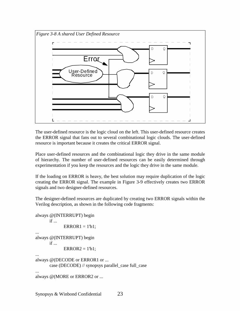
Synopsys & Winbond Confidential 23
The user-defined resource is the logic cloud on the left. This user-defined resource createsthe ERROR signal that fans out to several combinational logic clouds. The user-definedresource is important because it creates the critical ERROR signal.
Place user-defined resources and the combinational logic they drive in the same moduleof hierarchy. The number of user-defined resources can be easily determined throughexperimentation if you keep the resources and the logic they drive in the same module.
If the loading on ERROR is heavy, the best solution may require duplication of the logiccreating the ERROR signal. The example in Figure 3-9 effectively creates two ERRORsignals and two designer-defined resources.
The designer-defined resources are duplicated by creating two ERROR signals within theVerilog description, as shown in the following code fragments:
always @(INTERRUPT) beginif ...
ERROR1 = 1'b1;...always @(INTERRUPT) begin
if ...ERROR2 = 1'b1;
...always @(DECODE or ERROR1 or ...
case (DECODE) // synopsys parallel_case full_case...always @(MORE or ERROR2 or ...
Figure 3-8 A shared User Defined Resource
D Q
D Q
D Q
ErrorUser-Defined
Resource

Synopsys & Winbond Confidential 24
if (ERROR2 == ...
The first process that created the ERROR signal now creates an ERROR1 signal; asecond process creates the same logic and produces an ERROR2 signal. The ERROR1signal is used for the decoder, and the ERROR2 signal is used in the other process.
Selecting the optimal number of user-defined resources requires experimentation. Thisexperimentation is difficult if the logic spans a hierarchical boundary, since pins and portsare required to add intermodule resources. Keeping user-defined resources within amodule also minimizes the need to time-budget critical user- defined resources.
Do not optimize the number of user-defined resources in designs that are flattened duringcompile. Flattening is the process of reducing combinational logic to a boolean two-levelsum-of-products representation. Most designs (for example, datapath designs and designswith good structure) should not be flattened. Control or random logic often benefits fromflattening, and user-defined resource duplication occurs implicitly during flattening.
3.1.3.1 Example of Poor Partitioning
Figure 3-10 is an example of poor partitioning. In this example, the user-defined resourceis in a separate module. The hierarchy in the example contains four modules: one modulefor each of the combinational clouds and their corresponding registers, and one modulefor the user-defined resource. With this type of partitioning, the ERROR signals must be
Figure 3-9 Duplicate User Defined Resource
D Q
D Q
D Q
Error
User-DefinedResource
User-DefinedResource

Synopsys & Winbond Confidential 25
tightly time-budgeted, and module boundary changes are required to alter the number ofERROR signals.
3.1.3.2 Exception to the Recommendation
Relax this recommendation when the number of user-defined resources is easilydetermined.
3.1.4 Partition based on Design Goals
To achieve the best implementation results, separate modules with different design goals.Do not mix modules which are timing critical, for example, with modules that are areacritical. In this way, modules which require different synthesis or layout strategies can behandled more easily.
3.1.4.1 Area vs. Timing Critical Modules
In Figure 3-11, a section of the design that is not on the critical path is separated from thesection that contains the critical path. By doing so, area-based optimization can beperformed on the non-time critical logic. Similarly, special optimization and layout
Figure 3-10 A user-Defined Resource with Hierarchical Fanout
D Q
D Q
D Q
ERROR
User-Defined Resource

Synopsys & Winbond Confidential 26
considerations can be applied to the time critical module.
3.1.4.2 Example of Poor Area vs. Timing Partitioning
Figure 3-12 is an example of poor partitioning. In this example, both the critical path andthe non-critical sections of logic are combined in a single level of hierarchy. In this case,the area of the noncritical logic may be compromised to satisfy the tight timingconstraints of the overall design. This is because flattening and structuring options applyto an entire module, not just pieces of it. This example of poor partitioning also makes thetask of performing a hierarchical floorplan or layout more difficult by mixing designobjectives within a module.
Figure 3-11 Isolating Timing-Critical Logic from Area-Critical Logic
D Q D Q
set_max_area ??
CriticalPath
OffCriticalPath

Synopsys & Winbond Confidential 27
3.1.4.3 Random vs. Structured Modules
This recommendation is an extension of the previous one. Isolate logic with uniquecompile strategies as well as those that have unique compile goals. Isolating logic withunique goals makes obvious sense, but sometimes different optimization strategies arerequired for blocks that have the same goal. A data path and state machine might bothcontain critical paths, for example. However, the state machine might require stateoptimization and flattening, in addition to the default timing-driven structuring.Optimization attributes such as set_flatten and set_structure apply to modules, notsubportions.
Figure 3-13 diagrams a correctly partitioned design.
One module contains error-detection circuitry, which usually contains large exclusive-ORtrees. Because the module is so highly structured, it should not be flattened. The moduleon the right contains random logic, which might need to be flattened to make timing. Inthis example, the design is correctly partitioned because individual optimization attributescan be applied to both modules
Figure 3-12 Suboptimal Mix of Critical Path and Noncritical Logic
D Q
D QOff
CriticalPath
CriticalPath

Synopsys & Winbond Confidential 28
3.1.4.4 Example of Poor Compile Strategy Partitioning
Figure 3-14 shows an example of poor partitioning. This design contains a mix of logic.The random logic might need to be flattened, while the adder and muxing logic shouldnever be flattened. Because the logic is intermixed, these individual attributes cannot beapplied properly.
Figure 3-13 Logic Partitioned for Unique Optimization Strategies
Figure 3-14 Conflicting Optimization Requirements
D QD Q
set_flatten true
RandomLogic
ErrorCircuitry
D Q
D Q
RandomLogic
+

Synopsys & Winbond Confidential 29
3.1.4.5 Clock Generation Modules
Clock generation logic is typically handcrafted and often requires special timing analysis.Therefore, it is often recommended that clock generation logic be put into its own module,no matter what size. Follow the example shown in Figure 3-15 to partition clockgeneration modules.
3.1.4.6 Example of Poor Clock Module Partitioning
Figure 3-16 contains a design with functional logic and clock generation circuitry that iscombined. Because clocks must be handled carefully, this complicates the task ofsynthesis, timing analysis, floorplanning, and layout.
Figure 3-15 Isolate Clock Generation
Figure 3-16 A Locally Derived Clock
D Q
D Q
Clock Generation
Functional Logic
A
B
D Q
A
D Q
B

Synopsys & Winbond Confidential 30
3.1.4.7 Separate Asynchronous Logic
Asynchronous logic is sometimes technology-dependent, and typically requires gate-levelinstantiation and a special synthesis methodology. Partition your design so that theasynchronous logic is isolated from the synchronous logic.
An example of asynchronous logic would be a write-enable pulse generator for anasynchronous RAM, as shown in Figure 3-17. The write pulse generator could then beinstantiated with the asynchronous RAM to form a module that behaves like asynchronous RAM. Please note that the circuit in Figure 3-17 is provided merely as anexample of asynchronous logic -- not as a recommended implementation.
Asynchronous logic typically requires special test considerations and verificationstrategies. Check with your ASIC/FPGA vendor for recommendations and restrictionswith respect to your asynchronous logic.
3.1.4.8 Separate Finite State Machines
Similarly, isolate state machines. A state machine may benefit from the state machinecompiler or from a flattening optimization strategy. This is shown in Figure 3-18.
The graphic on the left represents a state machine. Modules that contain only statemachines simplify the state extraction and optimization process. Please refer to section4.5 (Finite State Machines) for FSM code examples.
Figure 3-17 Asynchronous Logic Example - Ram Write Pulse Generator
CLK WE_NWRITE
CLK
WRITE
WE_N

Synopsys & Winbond Confidential 31
3.1.4.9 Exceptions to the Recommendation
Always follow the recommendations for clock generation logic, but ignore the previousdesign-based recommendations for modules where the affect is insignificant. If only asmall amount of logic can be optimized for area, for example, leave that logic in the samemodule as the critical path and accept a slight increase in the design size. Always balancethe potential benefit of an additional module with the time it takes to create and maintainthe additional hierarchy.
3.2 Partitioning to Speed Up the Compile Process
Partitioning can also be used to minimize compile time. These recommendations arelisted below:
� Eliminate glue logic.� Maintain a reasonable gate size.� Maintain a reasonable number of levels in the hierarchy� Isolate point-to-point exceptions in the same module.
3.2.1 Eliminate Glue Logic
Ideally, a design hierarchy contains gates only at the leaf levels of the hierarchy tree.Figure 3-19 is a graphic example of this recommendation.
This hierarchical design contains four modules. No actual gates exist at the top level. Tomap the entire design, the modules will be individually synthesized and linked together atthe top level. Because the mapped modules can simply be linked together at the top level,this eliminates the extra time needed to compile at the top level.
Figure 3-18 An Isolated State Machine
D Q
State Machine

Synopsys & Winbond Confidential 32
Eliminating glue logic also simplifies script development. If only the leaf-level designscontain cells, an automated script mechanism only needs to compile and characterize leaf-level cells.
3.2.1.1 Example of Poor Partitioning
Figure 3-20 contains a poorly partitioned design that contains glue logic at the top level.
The design in Figure 3-20 contains three modules and a small AND gate. The AND gate
Figure 3-19 Glue-less Hierarchy
Figure 3-20 Glue Logic in a Design Hierarchy
D QD Q
D Q D Q
D QD Q
D Q

Synopsys & Winbond Confidential 33
is the glue logic. To compile this AND gate will take a considerable amount of time,because the lower-level designs are part of the hierarchy and need to be in memory. Toreduce the run time, either group the AND gate with the logic it drives, or into its ownlevel of hierarchy, with the group command.
3.2.1.2 Exceptions to the Recommendation
If you compile a design with a top-down hierarchical compile strategy (synthesize theentire design from the top level), the glue logic is not much of an issue. As in Figure 3-20,with a hierarchical compile, the extra AND gate between the partitions does not slowdown the compile process.
3.2.2 Maintain a Reasonable Module Size
How many gates should you have in a module? This question does not have an easyanswer. Module size is a secondary consideration when you compare it to the otherpartitioning recommendations. If you follow the general partitioning recommendations,most designs are naturally partitioned into reasonably sized modules. Try to maintain asize between 500 and 5000 gates per module. Module size affects the designer and thedesign as follows:
� Synthesis QOR� Compile Times� Iteration Times
The actual number of gates that you can synthesize in a single compile depends on yourCPU, RAM, Swap, etc.
Figure 3-21 shows a design that is well partitioned. The design modules are of reasonablesize. If design modules are too small, partitioning restricts the optimization algorithmswith artificial boundaries. Size also affects the amount of time synthesis compiles require,though it is not the only factor. In general, the more gates that need to be compiled, thelonger the synthesis process will take. Larger modules may be acceptable if sufficientCPU power and memory are available. However, if design modules are too big, synthesiscompiles may be prohibitively long. Finally, size also affects the design change process.Design changes usually change internal net and cell names and require recompilation.Smaller modules minimize the effects of name changes and reduce overall recompilationtime. However, balance this with the knowledge that an overly fine-grain partitioning willreduce Design Compiler's ability to optimize logic.

Synopsys & Winbond Confidential 34
3.2.2.1 Example of Poor Partitioning
Figure 3-22 contains a poorly partitioned design. Ten gates is too small a number for adesign module. Merge the block on the left with other logic. Modules that contain a verysmall number of gates severely limit optimization.
The block on the right is unnecessarily large. Design Compiler run times becomeprohibitive for such a large gate size on most machines.
Figure 3-21 Reasonable Design Size
Figure 3-22 Unreasonably Small and Large Desings
D Q
700 gates
1,800 gates
D Q
D Q
9,700 gates
10 gates
D Q

Synopsys & Winbond Confidential 35
3.2.2.2 Exceptions to the Recommendation
Again, module size is a secondary recommendation. Do not be overly concerned if adesign does not fall exactly within the 500-5000 gate range for functional reasons or otherpartitioning considerations.
3.2.3 Use a Reasonable Number of Levels of Hierarchy
Try to limit the number of levels of hierarchy in a reasonably sized module (500-5000gates) to two or three. Any more than this makes the code less readable, takes more timeto code, is more error prone, results in more files to manage, and results in longercompilation times.
Note that new levels of hierarchy are introduced whenever a Design Ware component isinferred (for bus-widths ≥ 4). The hierarchical boundaries can be removed using thedc_shell command ungroup [-flatten]. The -flatten switch may be required for complexDesign Ware components such as multipliers, because they contain levels of hierarchythemselves.
3.2.4 Isolate Point-to-Point Exceptions within the Same Module
If a design contains point-to-point exceptions to single-cycle timing requirements, keepthose exceptions within a module, as shown in Figure 3-23
Figure 3-23 A Local Single-Cycle Execption
D Q
D Q
D Q
O _reg
D_reg
set_false_path -from D_reg -to S_reg top
S_reg

Synopsys & Winbond Confidential 36
The design in Figure 3-23 contains a false path from the D_reg to the S_reg. Whenever apoint-to-point exception exists, it needs to be completely contained within a module ofhierarchy. Point-to-point exceptions occur when a command includes both the -to and the-from options. If a multicycle path occurs between a particular sets of registers, put allthese registers and the logic containing the paths within one level of hierarchy.
Point-to-point exceptions can slow down the compilation process considerably, inaddition to static timing analysis. By containing the point-to-point exception within onemodule, execution-time effect is minimized.
3.2.4.1 Example of Poor Partitioning
Figure 3-24 contains the same design as Figure 3-23 with an additional level of hierarchy.In Figure 3-24, the middle combinational logic cloud is in a separate level of hierarchycalled bottom. Because a false_path point-to-point exception is in the module bottom,characterize cannot accurately represent all the paths through pin B. If the false path is thelongest path through B, characterize incorrectly sets all paths from input pin B to false.
3.2.4.2 Exceptions to the Recommendation
You can relax the recommendation if you compile the design in Figure 3-24 with ahierarchical compile strategy from the top level of the design. With hierarchical compilethe recommendation is satisfied, since the single-cycle exception is wholly contained in
Figure 3-24 A Hierarchical Point-to-Point Exception
D Q
D Q
D Q
O _reg
D_reg
set_false_path -from D_reg -to S_reg top
B
bottom
S_reg

Synopsys & Winbond Confidential 37
the compiled hierarchy.
3.3 Partitioning to Simplify Scripts and Constraint Files
Strict partitioning guidelines, as embodied in this set of rules, will dramatically simplifythe set of scripts required for synthesis.
� Register all outputs� At chip-level create core logic, pad ring, and test hierarchy
3.3.1 Register All Outputs
To simplify the constraints and scripts process, register all outputs of a block as shown inFigure 3-25.
This partitioning recommendation dramatically simplifies time budgeting. The drivestrength of the inputs to an individual block is predictable and is equal to the drivestrength of the average flip-flop. The input delays from the previous block are predictableand are equal to the propagation delay of the flip-flop. Since one clock cycle is allocatedto the paths within each block, the constraints are identical for each module.
This partitioning approach supports a coding style that can improve simulation speed.With all outputs registered, you can describe a block with only edge-triggered processes.Each process would describe both combinational and sequential logic, but the sensitivitylist would contain only a clock and perhaps a reset pin. This approach speeds upsimulation, since the processes activate only once per clock cycle. The drawback is thatyou may not have as tight control over the inference of sequential devices (flip-flops) aswith a separate sequential process.
Figure 3-25 Registered Outputs
D Q D Q
set _drive drive_of <my _flop/Q> all_inputsset _input_delay 2 -clock CLK <input_port>

Synopsys & Winbond Confidential 38
3.3.1.1 Example of Poor Partitioning
Figure 3-26 contains an output signal that is connected directly to combinational logic. Itis an example of poor partitioning because output signal Q is not registered. This signalneeds a unique time budget to constrain and compile the leaf-level modules properly. Thetime budget includes the amount of time used in each module, the estimated drivestrength, and the estimated load. Although this style of partitioning is common and oftenfollows functional boundaries, it requires a lot more work to develop constraint scripts forcross-module combinational paths.
3.3.1.2 Exceptions to the Recommendation
You can relax this recommendation if your specification includes detailed timing budgetsdown to the module level. Balance between preserving a nonconforming functionalhierarchy and developing a more rigid time budget for those signals that cross throughblock boundaries in combinational logic.
In Figure 3-27, the two blocks contain datapath elements. The hierarchy is divided beforethe last mux. Since delays and time budgets are much more predictable in datapath logic,you may want to relax the registered output requirement for datapath sections in the logic.Be aware, however, that datapath elements may not be as predictable as they seem at first.An adder, for example, will have different timing from each input to each output,complicating the time budgeting process. When you consider the different potential adderimplementations (ripple, carry-lookahead, etc.), each with different timing, the timebudgeting process could become even more difficult.
Figure 3-26 A Combinational Inter-Block signal
D Q
Q
D Q
Synopsys & Winbond Confidential 39
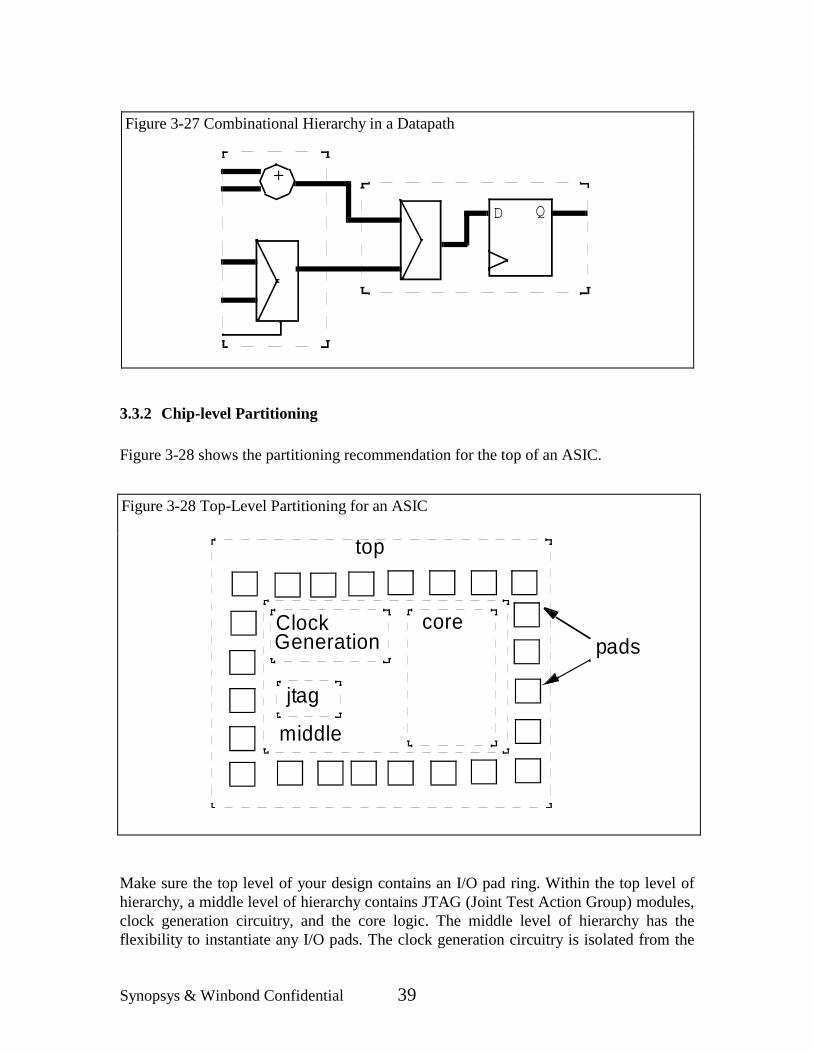
3.3.2 Chip-level Partitioning
Figure 3-28 shows the partitioning recommendation for the top of an ASIC.
Make sure the top level of your design contains an I/O pad ring. Within the top level ofhierarchy, a middle level of hierarchy contains JTAG (Joint Test Action Group) modules,clock generation circuitry, and the core logic. The middle level of hierarchy has theflexibility to instantiate any I/O pads. The clock generation circuitry is isolated from the
Figure 3-27 Combinational Hierarchy in a Datapath
Figure 3-28 Top-Level Partitioning for an ASIC
D Q
+
core
middle
jtag
ClockGeneration
top
pads

Synopsys & Winbond Confidential 40
rest of the design because typically it is handcrafted and carefully simulated.
This hierarchy arrangement is not a requirement, but allows easy integration andmanagement of the test logic, the pads, and the functional core. Insert scan in the logiccore, not at the top level of the design.
3.4 Commands that Manipulate Hierarchy
The best time to partition a design is during specification, before you write any Verilogcode. Unfortunately, you may not know the optimal hierarchy before you code a design. Ifartificial and suboptimal barriers exist in critical combinational logic paths, you canrearrange the hierarchy to eliminate the suboptimal interface.Design Compiler contains two commands, group and ungroup, to manipulate hierarchy.
You may use the group and ungroup commands to experiment with a design hierarchybefore modifying the design partitioning in the source code or to create a temporaryhierarchy change for optimization.
3.4.1 Ungroup
The ungroup command collapses hierarchy. Figure 3-29 shows a design before and afterusing the ungroup command.
On the left is a design top with three subdesigns. Each subdesign contains only onecombinational gate for simplicity. With such small partitions, the optimization process isseverely restricted. The ungroup command can remove the hierarchy. The ungroupcommand with the -all option removes all the hierarchy at this design level. At the right,the design is ungrouped and all cells are at the top level of the hierarchy.
You can use the ungroup command to ungroup a specific list of cells in the current design
Figure 3-29 Ungropuing a Design Hierarchy
Synopsys & Winbond Confidential 41
via the command ungroup -flatten {U1 U2} .The flatten switch collapses any hierarchy inthe cells U1 and U2.
3.4.2 Group
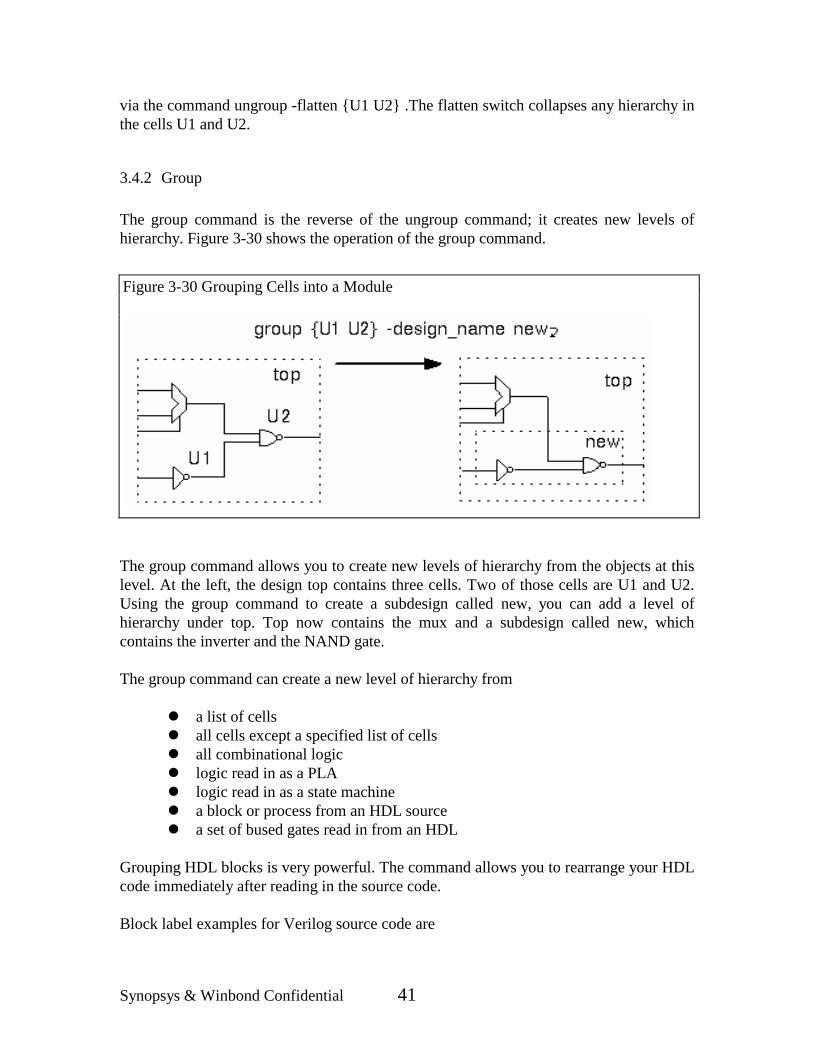
The group command is the reverse of the ungroup command; it creates new levels ofhierarchy. Figure 3-30 shows the operation of the group command.
The group command allows you to create new levels of hierarchy from the objects at thislevel. At the left, the design top contains three cells. Two of those cells are U1 and U2.Using the group command to create a subdesign called new, you can add a level ofhierarchy under top. Top now contains the mux and a subdesign called new, whichcontains the inverter and the NAND gate.
The group command can create a new level of hierarchy from
� a list of cells� all cells except a specified list of cells� all combinational logic� logic read in as a PLA� logic read in as a state machine� a block or process from an HDL source� a set of bused gates read in from an HDL
Grouping HDL blocks is very powerful. The command allows you to rearrange your HDLcode immediately after reading in the source code.
Block label examples for Verilog source code are
Figure 3-30 Grouping Cells into a Module

Synopsys & Winbond Confidential 42
// This is a named always blockalways @(CLK) begin : MY_PROCESS...end // MY_PROCESS
You can group individual HDL blocks with the -hdl_block option of the group command.To group a Verilog always block, you can group with the name of the block. The name ofthe block is MY_PROCESS in the preceding example. It can be grouped to create its ownlevel of hierarchy using the group command as follows:
group -hdl_block MY_PROCESS -design_name MY_BLOCK

Synopsys & Winbond Confidential 43
4. Implying Logic Structure
The following section discusses Verilog synthesis guidelines that pertain to implyinglogic structure in the style used to develop your model. They include:
� Unintentional Latches� If versus Case Statement� Code Organization and Optimization� Resource Sharing� Finite State Machines� Don't Care Inference� Repetitive Structures.
4.1 Unintentional Latches
When you use conditional statements like if or case, it is important to define them fully,to eliminate unwanted latches. Example 4-1 shows that an incompletely specified ifconstruct led to the creation of a latch on the output of a mux. The gate implementation isshown in Figure 4-1.
Example 4-1 Mux and Latch Inference
module MUX (A, B, SEL, Z);input A, B;input [1:0] SEL;output Z;reg Z;
always @(A or B or SEL) begin : MUX_PROCif (SEL == 2'b00)
Z = A;else if (SEL == 2'b11)
Z = B;end // MUX_PROC
endmodule

Synopsys & Winbond Confidential 44
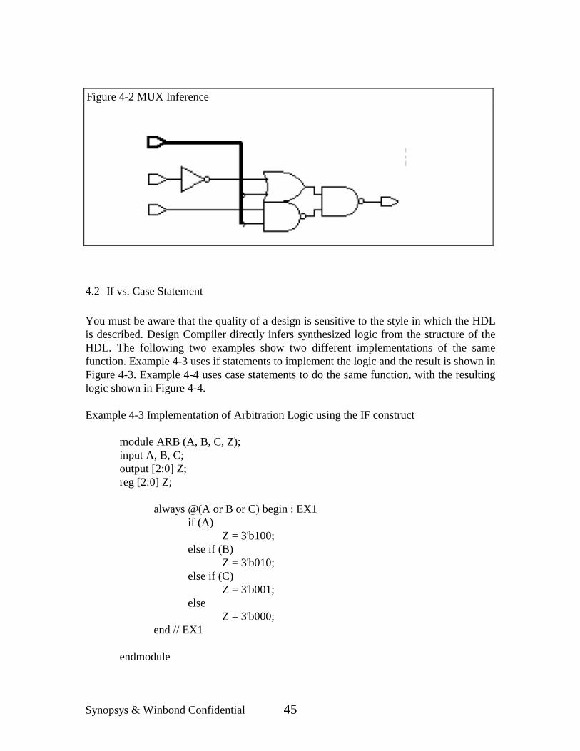
Example 4-2 shows a fully specified if construct that leads to a combinational only gateimplementation without the latch introduced in the previous code example. Figure 4-2shows the gate implementation.
Example 4-2 Mux Inference
module MUX (A, B, SEL, Z);input A, B;input [1:0] SEL;output Z;reg Z;
always @(A or B or SEL) begin : MUX_PROCif (SEL == 2'b00)
Z = A;else if (SEL == 2'b11)
Z = B;else
Z = 1'bx;end // MUX_PROC
endmodule
Figure 4-1 Mux and Latch Inference
Synopsys & Winbond Confidential 45
4.2 If vs. Case Statement
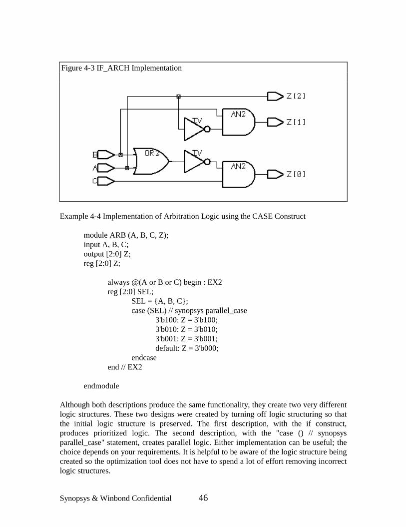
You must be aware that the quality of a design is sensitive to the style in which the HDLis described. Design Compiler directly infers synthesized logic from the structure of theHDL. The following two examples show two different implementations of the samefunction. Example 4-3 uses if statements to implement the logic and the result is shown inFigure 4-3. Example 4-4 uses case statements to do the same function, with the resultinglogic shown in Figure 4-4.
Example 4-3 Implementation of Arbitration Logic using the IF construct
module ARB (A, B, C, Z);input A, B, C;output [2:0] Z;reg [2:0] Z;
always @(A or B or C) begin : EX1if (A)
Z = 3'b100;else if (B)
Z = 3'b010;else if (C)
Z = 3'b001;else
Z = 3'b000;end // EX1
endmodule
Figure 4-2 MUX Inference
Synopsys & Winbond Confidential 46
Example 4-4 Implementation of Arbitration Logic using the CASE Construct
module ARB (A, B, C, Z);input A, B, C;output [2:0] Z;reg [2:0] Z;
always @(A or B or C) begin : EX2reg [2:0] SEL;
SEL = {A, B, C};case (SEL) // synopsys parallel_case
3'b100: Z = 3'b100;3'b010: Z = 3'b010;3'b001: Z = 3'b001;default: Z = 3'b000;
endcaseend // EX2
endmodule
Although both descriptions produce the same functionality, they create two very differentlogic structures. These two designs were created by turning off logic structuring so thatthe initial logic structure is preserved. The first description, with the if construct,produces prioritized logic. The second description, with the "case () // synopsysparallel_case" statement, creates parallel logic. Either implementation can be useful; thechoice depends on your requirements. It is helpful to be aware of the logic structure beingcreated so the optimization tool does not have to spend a lot of effort removing incorrectlogic structures.
Figure 4-3 IF_ARCH Implementation

Synopsys & Winbond Confidential 47
4.3 Code Organization & Optimization
Similar to writing efficient simulation models, the synthesis process is more efficientwhen the Verilog code is logically organized and prestructured for optimization. For theif-else construct, organize the code so that the latest arriving signals is the first test.Evaluating late arriving signal first ensures the least propagation delay through the gatesdue to levels of logic.
Structuring your Verilog statements can aid the synthesis logic optimization phasesignificantly. For example, you can minimize the compile time by manually sharingresources that you know in advance are advantageous to share. This circumvents the toolscapability to automatically determine whether it is appropriate to share a such resources.For example, the statements below will infer four adders:
x = a + c + by = c + a + d
By factoring out the subexpression, you can save one adder resource, as shown below:
t1 = a + cx = t1 + by = t1 + d
However, this type of code structure should not be used if signal "a" or "c" is a latearriving signal. In that case, the first structure is preferred allowing the tool to determinethe appropriateness of sharing based on the constraints.
Figure 4-4 CASE_ARCH Implementatopn

Synopsys & Winbond Confidential 48
Similarly, apply the loop invariant principle and place constant expressions outside of theloop. Here�s an example:
// wrong wayfor (i = 0; i <= 9; i = i + 1) begin : BAD_LOOP
PROC_DATA = PCI_DATA;FIFO(i) = CACHE(i-1);
end // BAD_LOOP
// right wayPROC_DATA = PCI_DATA;for (i = 0; i <= 9; i = i + 1) begin : GOOD_LOOP
FIFO(i) = CACHE(i-1);end // GOOD_LOOP
Moving constant assignments outside of the loop applies to synthesis because duringlogic optimization, a loop is unrolled and replaced by the inferred repetitive structure. If aconstant command is inside the loop, the logic optimization must spend timeunnecessarily reducing or eliminating the redundancies.
4.4 Resource Sharing
You must be aware of the benefits and the drawbacks of resource sharing and thendevelop your HDL code. Resource sharing is only used for logic whose timing goals havebeen met and whose next goal is area optimization. Let us examine the scope of resourcesharing with the assumption that the following block is a low speed block not in thecritical timing path of the module. Example 4-5 shows two processes to illustrate thescope of resource sharing:
Example 4-5 Two Processes To Show Scope Of Resource Sharing
always @(A1 or B1 or C1 or D1 or COND_1) begin : P1if (COND_1)
Z1 = A1 + B1;else
Z1 = C1 + D1;end // P1
always @(A2 or B2 or C2 or D2 or COND_2) begin : P2if (COND_2)
Z2 = A2 + B2;else
Z2 = C2 + D2;

Synopsys & Winbond Confidential 49
end // P2
Table 4-1 shows which resources inferred in the two processes in Example 4-5 can beshared. Table 4-1 shows that resources in the same process can be shared. Consequently,resources that are used in a mutually exclusive way must be inferred in the same processif the intent is to achieve area optimization through resource sharing. The followingexample is a code fragment that shows how to structure your code if you know you wantto explicitly share a resource.
if (CONDITIONAL_TST) beginT1 = A1;T2 = B1;
end // ifelse begin
T1 = C1;T2 = D1;
end // elseZ1 = T1 * T2;
There are cases where not all resources may be shared however. Example 4-6 is adataflow example that allows synthesis logic optimization to share some but not all, ofthe operators.
Example 4-6 Process With a Control Flow Conflict
always @(A or B or C or D or E or For G or H or I or J or OP) begin : LAB1
Z1 = A + B;case (OP) // synopsys parallel_case
2'b00: Z2 = C + D;2'b01: Z2 = E + F;
Table 4-1 Resource Sharing Example Between Two Processes
A1+B yes no no C1+D1 - no no A2+B n n - yesC2+D2 no no yes -
A1+B1 C1+D1 A2+B2 C2+D2
Allowed & Disallowed

Synopsys & Winbond Confidential 50
2'b10: Z2 = G + H;default: Z2 = I + J;
endcaseend // LAB1
Table 4-2 shows that the operator inferred through the addition of signals A and B cannotbe shared with any of the other addition operators. This is a result of the A+B operationnot being mutually exclusive with the other additions inferred in the process. Andremember, only enable resource sharing on the critical path if your timing goals are beingmet - use the Design Compiler variable to enable or disable resource sharing respectivelyas follows:
hlo_resource_allocation = constraint_driven (default)hlo_resource_allocation = area_onlyhlo_resource_allocation = none
The default setting (contraint_driven) is the best starting point. However, if you needmore information please refer to Design Compiler documentation for a detailedexplanation and proper use of these variables.
4.5 Finite State Machines
Consider what you are asking for when you code your designs. At a minimum, isolatesequential and combinational logic inference, i.e. use two separate always blocks. Youshould also isolate control flow and data flow logic. Isolation does not requirehierarchical partitioning. It is sufficient (even preferable) to structure the code accordingto these rules by breaking hardware functions up into independent processes or concurrentblocks. Consider the code fragment in Example 4-7. This code fragment is typical of asingle-process state machine. It does not separate sequential from combinationalinference, so all signals or variables assigned in the process are registered. It does not
Table 4-2 Resource Sharing Example With a Control Conflict
A+B - no no no no C+D no - yes yes yes E+F no yes - yes yes G +H no yes yes - yes
I+J no yes yes yes -
A+B C+D E+F G+H I+J
Allowed & Disallowed Sharings

Synopsys & Winbond Confidential 51
isolate control flow from data flow, so the state logic (state) and data outputs (y, count)are all combined into a large control or data flow graph.
Example 4-7 Single-Process State Machine - Not Recommendedalways @(posedge CLK) begin : NOT_RECOMMENDED
case (STATE) // synopsys parallel_case full_caseS0:
if (START)STATE <= S1;
COUNT <= 8'h00;Y <= 1'b0;
S1:if (COUNT == TERM_COUNT) begin
STATE <= S2;COUNT <= 8'h00;
end // ifelse if (WORD_MODE)
COUNT <= COUNT + 2;else
COUNT <= COUNT + 1;S2:
if (WORD_MODE)COUNT <= COUNT + 2;
......
Taking a closer look at the example, you know that the code infers an adder for each "+".You also know that CASE frames and complete IF and ELSE trees infer multiplexors.This design consists of many adders and many large multiplexors before the synthesisprocedures that implement resource selection and sharing. Each variable assigned in thecase frame has one large multiplexor. Each multiplexor has separate data and controlentries corresponding to each assignment in the case frame. Although this is a simpleexample, using the same style for a more complex state machine leads to a jumble ofcontrol and data flow which are difficult to structure and optimize.
Consider the alternative encoding in Example 4-8. This rather simple change can have ahuge effect on synthesis results. The counter inference, a pure data flow operation, isisolated from the state logic by placement in a separate process. Only the relevant controlconstructs are associated with the counter inference. The registered count signal dependson the state variable, so its inference remains in the state process for convenience. Noticethat only the necessary control constructs are left in the state process. All inferreddependencies now correspond to necessary hardware controls.
Example 4-8 State Machine with User-Defined Resource....// code in process 1 (combinatorial)

Synopsys & Winbond Confidential 52
if (WORD_MODE)NEXT_COUNT = COUNT + 2;
elseNEXT_COUNT = COUNT + 1;
....
....// code in process 2 (sequential)case (STATE) // synopsys parallel_case full_case
S0:if (START)
STATE <= S1;COUNT <= 8'h00;Y <= 1'b0;
S1:if (COUNT == TERM_COUNT) begin
STATE <= S2;COUNT <= 8'h00;
end // ifelse
COUNT <= NEXT_COUNT;S2:
COUNT <= NEXT_COUNT;......
Partition HDL code intelligently and use the group -hdl_block command to isolate codefragments for optimization during synthesis when necessary.
For FSMs the best synthesis results may be achieved via Synopsys FSM extractioncapability. The actualy FSM extraction methodology is beyond scope here, but weprovide a Verilog code example (Example 4-9) here in order to demonstrate proper use ofthe Synopsys compile directives that enable use of the FSM extraction capability.
Example 4-9 FSM with Compile Directives for Extraction
module MACHINE (CLK, X, CURRENT_STATE, Z);
input CLK;input X;output [1:0] /* synopsys enum MY_STATES */ CURRENT_STATE;reg [1:0] /* synopsys enum MY_STATES */ CURRENT_STATE;
// synopsys state_vector CURRENT_STATEoutput Z;reg Z;
reg [1:0] /* synopsys enum MY_STATES */ NEXT_STATE;
// synopsys state_vector NEXT_STATE

Synopsys & Winbond Confidential 53
reg PREVIOUS_Z;
parameter [1:0] // synopsys enum MY_STATES SET0 = 2'b00, HOLD0 = 2'b01, SET1 = 2'b10;
// Synchronous elements (flip-flops).always @(posedge CLK)
begin : SYNC CURRENT_STATE <= NEXT_STATE; PREVIOUS_Z <= Z; end // SYNC
// Combinational logicalways @(CURRENT_STATE, X, PREVIOUS_Z)
begin : COMB case (CURRENT_STATE) SET0: begin Z = 1'b0; NEXT_STATE = HOLD0; end HOLD0: begin Z = PREVIOUS_Z; if (!X) NEXT_STATE = HOLD0; else NEXT_STATE = SET1; end SET1: begin Z = 1'b1; NEXT_STATE = SET0; end endcase; end // COMB
endmodule
You should note the following points with respect to Example 2-16: there is one processeach for the combinational and sequential inference sections, and the use of the compiledirectives enum and state_vector.
4.6 Don't-Care Inference (casex)

Synopsys & Winbond Confidential 54
You can greatly reduce circuit area with don't-cares in your design. Don't care conditionscan show up two ways in your designs: either on the right-hand side of a signalassignment or as one or more of the enumerated cases. When on the right-hand side, themethod is fairly simple and Example 4-10 shows a typical use of don't-care inference. Beaware, that you may use the set_flatten -true command to get additional optimization ofthe combinational logic.
Example 4-10 Don't Care Inference in a BCD Decoder (Simple)
case (BCD) // synopsys parallel_case4'h0: LED = 7'b1111110;4'h1: LED = 7'b1100000;4'h2: LED = 7'b1011011;4'h3: LED = 7'b1110011;4'h4: LED = 7'b1100101;4'h5: LED = 7'b0110111;4'h6: LED = 7'b0111111;4'h7: LED = 7'b1100010;4'h8: LED = 7'b1111111;4'h9: LED = 7'b1110111;default: LED = 7'bxxxxxxx; // use of don�t care
endcase
The more complex use of don't care conditions arises when the don't care is one or moreof the enumerated cases. Here it is necessary to the Verilog casex construct. The nextthree examples illustrate proper and improper use.
Example 4-11 Don't Care Inference for a Decoder8_a (Poor Result: Improper Logic)module decoder8_a(A, Z);
/* Uses case statement and an attempt to optimize based on don�t care conditions.Result is improper logic. Z decodes to 3'b000 forall input states ! */
parameter N = 8;parameter log2N = 3;
input [N-1:0] A;output [log2N-1:0] Z;
reg [log2N-1:0] Z;
always @(A) begin: encode
case (A) // synopsys full_case parallel_case 8'b00000001 : Z = 3'b000;

Synopsys & Winbond Confidential 55
8'b0000001x : Z = 3'b001; 8'b000001xx : Z = 3'b010; 8'b00001xxx : Z = 3'b011; 8'b0001xxxx : Z = 3'b100; 8'b001xxxxx : Z = 3'b101; 8'b01xxxxxx : Z = 3'b110; 8'b1xxxxxxx : Z = 3'b111; endcase
endendmodule
Example 4-12 Don't Care Inference for a Decoder8_b (Poor Result: Latches)
module decoder8_b(A, Z);
/* Uses casex statement and attempt to optimize based on don�t careconditions, but the case is not fully specified (A=8�h00 ismissing). Result is unintentional latches on output Z ! */
parameter N = 8;parameter log2N = 3;
input [N-1:0] A;output [log2N-1:0] Z;
reg [log2N-1:0] Z;
always @(A) begin: encode
casex (A) 8'b00000001 : Z = 3'b000; 8'b0000001? : Z = 3'b001; 8'b000001?? : Z = 3'b010; 8'b00001??? : Z = 3'b011; 8'b0001???? : Z = 3'b100; 8'b001????? : Z = 3'b101; 8'b01?????? : Z = 3'b110; 8'b1??????? : Z = 3'b111; endcase
endendmodule
Example 4-13 Don't Care Inference for a Decoder8_c (Good Result)
module decoder8_c(A, Z);/* Uses casex statement and proper synopsys directives to optimize

Synopsys & Winbond Confidential 56
based on don't care conditions. Result is correct ! */
parameter N = 8;parameter log2N = 3;
input [N-1:0] A;output [log2N-1:0] Z;
reg [log2N-1:0] Z;
always @(A) begin: encode
casex (A) // synopsys full_case parallel_case 8'b00000001 : Z = 3'b000; 8'b0000001x : Z = 3'b001; 8'b000001xx : Z = 3'b010; 8'b00001xxx : Z = 3'b011; 8'b0001xxxx : Z = 3'b100; 8'b001xxxxx : Z = 3'b101; 8'b01xxxxxx : Z = 3'b110; 8'b1xxxxxxx : Z = 3'b111; endcase
endendmodule
4.7 Repetitive Structures
In a dataflow modeling style, you typically describe individual functional blocks asparallel processes. This style is also known as a sequential modeling style becausestatements inside a process are executed sequentially rather than concurrently. Thefollowing example is a code fragment that uses a for loop to handle a repetitive structurethat adds several product terms (m to be exact) to produce a sum of products.
sum_of_prod = 0; // initialize to zerofor (m = 0; m < NUM_PRODUCTS; m = m + 1) begin : SOP_LOOP
SUM_OF_PROD = SUM_OF_PROD + PRODUCT_TERM(m);end // SOP_LOOP
The for loop in this example is very effective at reducing the number of statementsneeded to implement the necessary repetitive structure.
4.8 Avoid Redundant Logic and Subexpressions

Synopsys & Winbond Confidential 57
Note that the HDL Compiler parser has very limited ability to recognize comonsubexpressions on its own. Look for common subexpressions in your code, and separatethem into separate expressions. The following examples illustrates this.
// Bad - Will synthesize four addersX = A + B + C;Y = D + C + A;
// Better - Will only synthesize three addersT = A + C;X = T + B;Y = T + D;
// Bad - Will synthesize 4 multipliers and 3 addersZ = A*C + A*D + B*C + B*D;
// Better - Will synthesize 1 multiplier and 2 addersZ = (A + B) * (C + D);
You can also use parantheses to denote the common subexpressions to guide the HDLCompiler parser, thus allowing common subexpression sharing (CSE). The followingexamples allow CSE to occur.
Z = (A + B) + DZ = D + (A + B)
4.9 Inferring the Correct Register
Registers with either synchronous or asynchronous resets, are inferred by the structure ofa sequential process. To guide DC to choose the correct register, use attributes in yourcode, as described below.
4.9.1 Registers with Synchronous Reset
Use the attribute sync_set_reset to instruct DC to select a register with a synchronousreset, when implementing the sequential logic. This is illustrated below.
module DFF_SYNC_RESET (DATA, CLK, S_RESET, Q);input DATA, CLK, S_RESET;output Q;reg Q;
// synopsys sync_set_reset "S_RESET"

Synopsys & Winbond Confidential 58
always @(posedge CLK)if (S_RESET = 1'b1)
Q <= 1'b0;else
Q <= DATA;
endmodule
4.9.2 Registers with Asynchronous Reset
No attribute is needed to guide DC in inferring an asynchronous reset register in thedesign. The structure of the code is all that is necessary to infer a register with anasynchronous reset. You may consider including the async_set_reset attribute as shownbelow.
module DFF_ASYNC_RESET (DATA, CLK, A_RESET, Q);input DATA, CLK, A_RESET;output Q;reg Q;
// synopsys async_set_reset "A_RESET"
always @(posedge CLK or posedge A_RESET)if (S_RESET = 1'b1)
Q <= 1'b0;else
Q <= DATA;
endmodule
4.10 Structure for Minimum Delay
If your goal is to speed up your design, arithmetic optimzations implemented during thecompile process can minimize the delay through an expression tree by rearranging thesequence of operations. Figure 4-5 displays the default tree structure Design Compilerbuilds for either signal assignment (no parantheses or parantheses as shown).
The default tree structure is the type of structure the forms the starting point for synthesisand provides the minimum delay structure if the signal D arrives late with repect to theother input signals. Furthermore, during the structuring phase of the compile process,Design Compiler will automatically restructure the design such that the latest arrivingsignal would be placed at the last adder. However, if all the input signals arrive a roughlythe same time, a better structure would be that shown in Figure 4-6.

Synopsys & Winbond Confidential 59
The end result here is that by using parantheses, factoring common subexpressions, andsimilar types of code structuring you can define the synthesis structure starting point andpossibly obtain a better quality of results
4.10.1 Inferring Tri-State Drivers
One application of the verilog if statement is to describe data that is conditionallyavailable. For example, tri-state logic is synthesized on the output driver when the outputsignal is assigned "Z" in either of the if clauses shown below:
always @ (FROM_TABLE or ENABLE);
Figure 4-5 Default Tree Structure
Figure 4-6 Balanced Tree Structure
A B
C
Z
D
+
+
+
Z = A + B + C + D;
Z = ((A + B) + C + D;
oryields
Synthesis start point
A B C
Z
D
++
+Z = (A + B) + (C + D);yields
Synthesis start point

Synopsys & Winbond Confidential 60
begin: DRIVE_OUTPUTif (ENABLE)
TO_BUS = FROM_TABLE;else
TO_BUS = 8'bZ;end // DRIVE_OUTPUT
It's important to know that each always block can generate only one Tri-state buffer as anoutput driver. Thus multiple always blocks are required to infer multiple Tri-state drivers.Example 4-14 shows two ways of inferring two Tri-state drivers for the same outputsignal.
Example 4-14 Multiple Tri-state Driver Inference
module TRISTATE_A (A, B, SELA, SELB, OUT1);input A, B, SELA, SELB;output OUT1;reg OUT1;
always @(SELA or A)OUT1 = (SELA)?A: 1'bz;
always @ (SELB or B) begin
if (SELB)OUT1 = B;
elseOUT1 = 1'bZ;
endendmodule
module TRISTATE_B (A, B, SELA, SELB, OUT1);input A, B, SELA, SELB;output OUT1;wire OUT1;
assign OUT1 = (SELA)?A:1'bz;assign OUTB = (SELB)?B:1'bz;
endmodule
Example 4-14 shows three coding styles of inferring multiple tri-state drivers. ModuleTRISTATE_A shows the use of the conditional operator (?) and the if-then-else construct.Module TRISTATE_B shows the use of the continuous signal assignment statement.

Synopsys & Winbond Confidential 61
The Verilog language also allows another method of inferring Tri-state drivers: the casezstatement. The casez statement is a type of case statement and allows a multipath branchin logic according to the value of an expression, just like the case statement. Thedifferences between the case statement and the casez statement are the keyword and theway the expressions are processed.
casez (what_is_it) 2'bz0: begin
// accept anything with least significant bit zero it_is = even; end 2'bz1: begin
// accept anything with least significant bit one it_is = odd; end
endcase
We see that Verilog allows the "Z-state" to be contained in the enumerated case items.But note it is illegal for the casez (expression) to be completely in a tri-state conditionitself as shown in this example:
what_is_it = 2'bzz;casez (what_is_it)
2'bz0: beginit_is = even;
. . .
WarningSynopsys DC won't allow normal 2-state signals to be driven from multiple always blocks,but some Verilog simulators might allow it.
It is also equally important to note that some Verilog simulators allow Tri-state drivensignals and normal 2-state logic to be driven from multiple always blocks (assuming thesignal is not of wired logic type). The former is legal as shown in Example 4-14, but isillegal for Synopsys Design Compiler for the latter case.
NoteTesting for the Z-state will restrict CycloneTM to operate in 4-state mode, instead of thefaster 2-state mode.
Synopsys & Winbond Confidential 62
5. Safe Coding
The following section discusses Verilog synthesis guidelines that pertain to implyinglogic structure in the style used to develop your model. These guidelines are techniquesthat Synopsys has found to work well in setting a safe-zone of operation for synthesismodel development. There will be times you may need to deviate from the safe codingguidelines because of trade-offs you made during the design process. When you dodeviate from the safe-zone of operation, verify that there is not a better alternative. Justifyyour reasoning during the review process. The safe coding techniques include:
� One Clock per Module� Separate Sequential & Combinational Processes� Proper Sensitivity Lists� Blocking vs. Nonblocking Assignments� Named Association� Instantiation of Sensitive or Asynchronous Circuits� Avoiding Concurrent Verilog Statements� Reset Strategy Consistency� Black Box Cells� Initialization Considerations� Mixed Edge Sensitivity� Constant Propagation
5.1 One Clock per Module
In general, a design with multiple clocks should be partitioned into subdesigns with onlyone clock in each submodule. The benefits of having a single clock per module include:
� Synthesis process is designed to perform logic optimization based on a singleclock, or multiple fully synchronous clocks
� Synthesis constraints are simpler with a single clock module� Asynchronous logic is often introduced as a result of a logic with
asynchronous clock interfaces.
Design Compiler does allow multiple harmonically related synchronous clocks to bepresent in a design. Each clock domain forms a unique path group and allows uniquetiming constraints to be specified for the compile process. Hence, multiple synchronousclocks are a tractable problem and many designs require only minor logic optimization tomeet the constraints of a second synchronous clock in a design. When there are signaltransfers between clock domains it may be necessary to use the set_multicycle_pathcommand (please refer to the Design Compiler Reference manual for more details). Thisis typically the case if the clock is controlling simple logic or is relatively slow for theprocess technology. This concept does not apply to high-speed clock synchronizer circuits,

Synopsys & Winbond Confidential 63
for which careful partitioning, coding, and instantiation may be required.
5.2 Separate Sequential & Combinational Processes
Synopsys recommends separating sequential logic from combinational logic with separatedistinct processes. The potential pitfall is to inadvertently infer unnecessary sequentialelements by placing sequential signal assignments in the sequential process. Example 5-1implies the use of seven flip flops: three to hold the value of COUNT, and one each tohold RESULT, AND_BITS,OR_BITS, XOR_BITS.However, the value of RESULTdepends on the value of registered signal COUNT. Hence, there is no need to also registerAND_BITS, OR_BITS, and XOR_BITS.
Example 5-1 Code That Implies Extra Unwanted Registers
module count (CLOCK, RESET, RESULT);input CLOCK, RESET;output RESULT;reg RESULT, AND_BITS, OR_BITS, XOR_BITS;reg [2:0] COUNT;
always @(posedge CLOCK) begin : BAD_EXAMPLEif (RESET) begin
COUNT <= 0;RESULT <= 0;
endelse begin
COUNT <= COUNT + 1;AND_BITS <= & COUNT; // AND_BITS gets a Flip FlopOR_BITS <= | COUNT; // OR_BITS gets Flip FlopXOR_BITS <= ^ COUNT; // XOR_BITS get a Flip FlopRESULT <= AND_BITS & OR_BITS & XOR_BITS;
endend // BAD_EXAMPLE
endmodule
The best way to avoid introducing this problem is to use two separate processes. Example5-2 demonstrates the correct way to infer the sequential logic separate from thecombinational logic.
Example 5-2 Code Without Implying Extra Registersmodule count (CLOCK, RESET, RESULT);
input CLOCK, RESET;output RESULT;

Synopsys & Winbond Confidential 64
reg RESULT, AND_BITS, OR_BITS, XOR_BITS;reg [2:0] COUNT;
always @(posedge CLOCK) begin : SEQ_BLKif (RESET) begin
COUNT <= 0;RESULT <= 0;
endelse begin
COUNT <= COUNT + 1;RESULT <= AND_BITS & OR_BITS & XOR_BITS;
endend // SEQ_BLK
always @(COUNT) begin : COMB_BLKAND_BITS = & COUNT;OR_BITS = | COUNT;XOR_BITS = ^ COUNT;
end // COMB_BLK
endmodule
5.3 Proper Sensitivity Lists
A sensitivity list is a Verilog construct that limits the execution of a process. Whenwriting a behavioral model for simulation purposes only, you may choose to restrict thelist of signals to a subset of all signals used. This is commonly done for eventminimization in simulation models because knowledge of a particular circuit may allow it.However, if the simulation model is to be used to compare the behavior of acorresponding RTL model, we recommend specifying complete sensitivity lists forcombinational processes. Sequential process sensitivity lists need only be sensitive toclock and reset signals. The following example code fragment shows an incompletesensitivity list:
always @(A or B) begin : MY_PROCMY_OUT = A & B & C;
end // MY_PROC
Although rather simple, this example could have a dramatic affect on functionality bypossibly producing a mismatch between simulation model and gate level model results.This error typically can be introduced when a new signal is added to a combinationalprocess and the designer forgets to update the sensitivity list. The error is typically foundduring the synthesis analyze/elaborate steps. If ignored, a post-synthesis vector mismatchmay occur.

Synopsys & Winbond Confidential 65
It is important for the process to be sensitive to signals that are read. If it is not, synthesisissues the following warning during elaboration:
Warning: Variable 'C' is being read in routine INV line 12 in file '/home/inv.v', butdoes not occur in the timing control of the block which begins there. (HDL-180)
It is a wise idea to investigate such warnings since there is the possibility that acorresponding simulation model specified an incomplete process sensitivity list.It is also a good idea to run your design through the HDL Compiler (analyze andelaborate only) before you simulate. This will immediately warn you of missing variablesin sensitivity lists, and multiply driven signals, which otherwise could take a long time todebug in simulation.
5.4 Blocking vs. Non-blocking Assignments
Blocking procedural assignments (=) behave more like software variables in that the codeexecutes sequentially versus hardware which executes concurrently. Thus, as in software,the execution of blocking assignments are order dependent, and execution of subsequentlines of code are blocked until values are assigned. Therefore, blocking assignments aremade immediately. Using blocking assignments improves simulation speed.
Non-blocking procedural assignments (<=) are more like hardware in that they emulateconcurrent operations. A non-blocking assignment does not block execution ofsubsequent lines of code. The assignments are not made immediately, but are insteadscheduled to be made concurrently when the process terminates. As a result, they areinsensitive to assignment order.
Use non-blocking assignments for all inferred registers (flip-flops, latches); and useblocking assignments for combinatorial outputs and intermediate local variableassignments. This is illustrated in Example 5-3.
Example 5-3 Example of Blocking vs. Non-blocking
always @(posedge CLK) begin : SHIFT_REGST1_REG <= DATA_IN;ST2_REG <= ST1_REG;OUT_REG <= ST2_REG;
end // SHIFT_REG
always @(A or B or SEL) begin : MY_MUXif (SEL == 1'b0)
OUT = A;else

Synopsys & Winbond Confidential 66
OUT = B;end // MY_MUX
To illustrate the difference between blocking and non-blocking, consider the design of asimple two-bit shift register. The desired circuit is shown in Figure 5-1.
The Verilog code for the shift register, using non-blocking assignments is shown in thefollowing example.
Example 5-4 Proper Use of Non-blocking Assignment
// Proper use of non-blocking assignmentalways @(posedge CLK) begin : GOOD_SHIFT_REG
REG0 <= DATA; // REG0 scheduled to get DATAREG1 <= REG0; // REG1 scheduled to get REG0
end // GOOD_SHIFT_REG Concurrent assignments made at end.
Using non-blocking assignments, REG0 and REG1 are updated concurrently insimulation upon termination of the process, and get the previous values of DATA andREG0 respectively. The code will synthesize to the desired circuit shown in Figure 5-1.
What happens if blocking assignments are used instead of non-blocking assignments inthe shift register example? The logic will not synthesize to the desired circuit. This isillustrated in Example 5-5 and Figure 5-2.
Example 5-5 Improper Use of Blocking Assignment
Figure 5-1 Simple Two-Bit Shift Register
DATA
CLK
REG0
REG1

Synopsys & Winbond Confidential 67
// Improper use of blocking assignmentalways @(posedge CLK) begin : BAD_SHIFT_REG
REG0 = DATA; // REG0 gets DATA immediatelyREG1 = REG0; // REG1 gets DATA since REG0 = DATA
end // BAD_SHIFT_REG
Each time this process terminates, REG0 and REG1 will both contain the value of DATA.The circuit synthesized from the code in Example 5-5 is not the desired shift register, butrather a parallel-load register, as shown in Figure 5-2.
Suppose each of the above assigments were made in two separate processes. Using non-blocking assignments would guarantee correct simulation. If blocking assignments wereused however; the simulation results would be non-deterministic. The order in which thesignals get updated would be arbitrary. Note however, that the circuit would synthesize tothe desired shift register, as long as there is only one assignment made per process.
What happens if non-blocking assignments are used instead of blocking assignments forcombinational outputs of processes? The logic will still simulate and synthesize correctly,but simulation performance will suffer.
5.5 Ordered vs. Named Association
When instantiating components in a structural model, specify port connections explicitly(name-based) versus implicitly (positional). Although it may be more compact orconvenient to define the mappings implicitly, it is also more susceptible to errors, since
Figure 5-2 Two-Bit Parallel-load Register
DATA
CLK
REG1
REG0

Synopsys & Winbond Confidential 68
you must rely on specifying the correct order. Explicit mapping statements are moreverbose, but at the same time they are self-documenting and less error-prone, since theorder of assignment statements in the mapping doesn't matter.
Example 5-6 Implicit and explicit map styles
// Implicit Port MappingSOMEBLOCK U1 (A,B,C,CLK2); // Legal, but error prone:
// Explicit Port Mapping - BetterSOMEBLOCK U1 (.CLK(CLK2),.A(DATA),.B(CONTROL), .C(BUS));
For name-based association, the component port names must exactly match the declaredcomponent's port names. For positional association, the actual port expressions must be inthe same order as the declared component's port order.
Synopsys strongly recommends the use of the associative style since it is much less errorprone and easier to maintain. For example, if the module declaration associated with theSOMEBLOCK component (described in the previous example) reorders its declared ports,it does not require a change in the component instantiation. The positional associationstyle would require a code change in both places. A functional error is introduced (if youforget to update the component instantiation statement).
5.6 Instantiation of Sensitive or Asynchronous Circuits
Hierarchy in Verilog is specified by instantiating submodules within a module (as inExample 5-6). If it's necessary to instantiate gates from the target technology library,when possible maintain technology independence by instantiating Synopsys GTECH cells(refer to Section 1.6.3). Using GTECH maintains technology independence since the cellsare represented in the Synopsys intermediate database format.
This technique is useful if your design is classified as a critical/sensitive circuit, anasynchronous circuit, or if you know the exact logic structure desired. Examples includethe following: an external processor interface may be a critical circuit, a gated clockmodule is certainly an asynchronous circuit, and an on-chip interface to a logic core mayrequire a particular logical structure.
You can use Design Compiler to associate an instantiated component with the specifictechnology library cell(s) using Synopsys attributes (e.g. set_map_only, orset_dont_touch). It is important to remember that you will need to simulate your Veriloggate-level design, and will need a simulation model of some sort for all instantiatedcomponents.
One reason it may be dangerous to infer logic gates on asynchronous circuits (e.g. gated
Synopsys & Winbond Confidential 69
clock line) from your Verilog source code is that Design Compiler does not guarantee thatlogic circuit produced is not hazard-free (i.e. no glitches). Hence, if you understand acircuit and can prove it's a hazard free design, it's recommended that you considerinstantiating the gates for such a critical circuit and to apply full timing simulation toensure the circuit is hazard-free and implements the desired functionality. Example 5-7 isan asynchronous counter design. There's an asynchronous reset inferred in the alwaysblock, and of special interest is the signal GATED_CLK. The counter is enabled byANDing the CLK and ENABLE signals. This technique will only work correctly if youcan guarantee the timing relationship between the control signals (ENABLE and RESET)and the clock signal CLK, and if the control signals are glitch-free. The end result here isthat it may easier to instantiate the exact logic gates with a dont_touch attribute(s) toprevent Design Compiler from swapping gates or restructuring the circuit.
Example 5-7 Asynchronous Counter Design
module COUNT (RESET, ENABLE, CLK, Z);input RESET, ENABLE, CLK;output [2:0] Z;reg [2:0] Z;
wire GATED_CLK = CLK & ENABLE; // Async Signal
always @ (posedge GATED_CLK or posedge RESET) begin: SEQif (RESET) begin
Z <= 1'b0;endelse beginif (Z == 3'd7) begin
Z <= 1'b0;endelse begin
Z <= Z + 1'b1;endend
end // SEQendmodule
5.7 Avoid Continuous Signal Assignments
Continuous assignments are executed in no defined order and synthesize to combinationallogic. To facilitate the option to repartition in synthesis, and to improve code readability,you should place the logic in a combinational always block instead. The following codefragments illustrate this for a 1-bit full adder.

Synopsys & Winbond Confidential 70
// Continuous Assignment Example -- Not Recommendedassign SUM = A_IN ^ B_IN ^ C_IN;assign C_OUT = (A_IN & B_IN) | (B_IN & C_IN) | (A_IN & C_IN);
// Combinational process -- Recommendedalways @(A_IN or B_IN or C_IN) begin : FULL_ADDER
SUM = A_IN ^ B_IN ^ C_IN;C_OUT = (A_IN & B_IN) | (B_IN & C_IN) | (A_IN & C_IN);
end // FULL_ADDER
5.8 Reset Strategy Consistency
The minimum area D flip-flop cell in most libraries does not have a set or reset pin tocontrol initialization. Therefore, a circuit using such a cell must be designed to be self-initializing to get to a known state within a predetermined number of clock cycles.Synopsys recommends inferring these types of cells only when the designer is 100 percentcertain that the circuit will self-initialize with no ambiguity. If this condition cannot bemet, then the designer must infer either sequential cells with synchronous orasynchronous set/resets pins in a module.
The method of inferring registers with either synchronous or asynchronous resets (orpresets) is described in Section 4.9.
Check your target technology in advance to see what type of registers are available. Alsocheck with your ASIC/FPGA vendor to see if a particular reset strategy is recommended.
5.9 Black Box Cells
Black-box cells are complex cells in the design with functionality not known to DesignCompiler. The functionality of these complex cells (such as RAMs, multiple latches orflip-flops in parallel with common enables or clocks) cannot be described in the librarysyntax supported by Synopsys, which is why they are labeled as black-boxes. Since thetranslate command replaces cells in the design with the closest matching cells in thetarget library, black-box cells cannot be translated. There is no way to determine a matchfor them.
In some cases, black-box cells cannot be avoided. For example, on-chip memory (e.g.RAM or ROM) needs to be modeled and included in your simulation model. For otherblackbox cells that are instantiated in your RTL synthesis model, consider developing aninterface timing specification (ITS) model that describes the pin-to-pin timing delays sothat static timing analysis on the black box timing paths may be computed. Refer to theLibrary Compiler Reference Manual (Interface Timing of Complex Sequential Blocks)for more details.

Synopsys & Winbond Confidential 71
5.10 Don't Initialize Signals
The Verilog language provides the ability to initialize registers to a known value at thebeginning of simulation time, in an initial process. This method is convenient, and maybe used in behavioral testbenches, but should not be used in synthesizable RTL code.Initial processes are not supported in synthesis, and will result in the following errormessage.
Error: Initial statement not supported near symbol "initial" on line 6 in file"mult.v" (VE-19)
Any synthesizable registers that must be initialized to a known value, should be done sousing a reset strategy.
The following examples illustrate the use and misuse of initialization blocks.
Example 5-8 Initialization of Testbench Code is Okay -- Not Synthesized
initial begin : TESTBENCH_INITCLK = 0;RESET = 1;#40 RESET = 0;...
end // TESTBENCH_INIT
always begin : TESTBENCH_PROC#10 CLK = !CLK;...
end // TESTBENCH_PROC
Example 5-9 Don't Initialize Synthesizable Code -- Synthesis Error!
// Bad Example: Results in Synthesis Errorinitial begin : COUNTER_INIT
COUNT = 0;end // COUNTER_INIT
always @(posedge CLK) begin : COUNTER_PROCCOUNT = COUNT + 1;
end // COUNTER_PROC
Example 5-10 Initialization Example using Synchronous Reset

Synopsys & Winbond Confidential 72
always @(posedge CLK) begin : COUNTER_PROCif (RESET == 1'b1)
COUNT = 0;else
COUNT = COUNT + 1;end // COUNTER_PROC
5.11 Don't Use Mixed-Edge Sensitivity
The Synopsys synthesis tools do not support processes which are triggered on both edgesof the same clock signal. The following example would simulate as coded, but wouldresult in a synthesis error.
Example 5-11 Mixed-Edge Sensitivity Example
always @(posedge CLK or negedge CLK) begin : DBL_EDGE_REGQ = D;
end // DBL_EDGE_REG
Analyzing this code in Design Compiler produces the following error message.
Error: Depending on 2 edges of same variable "CLK" not supportednear symbol ")" on line 18 in file dbl_edge.v (VE-22)
5.12 Constant Propagation
Pins on subdesigns that are driven to constants, should be hard-wired to the constantvalue at the lowest level of hierarchy. Design Compiler can't eliminate redundant logic, oroptimize logic using the constant, if it crosses a hierarchical boundary.
For example, suppose you wanted to compare an address to a constant, hard-wired deviceid. The first example illustrates the results of synthesis for a module in which the constantis propagated through a primary input.
Example 5-12 Propagating a Constant Across a Hierarchical Boundary
module COMP (ADDR, DEV_ID, MATCH);input [7:0] ADDR, DEV_ID;output MATCH;reg MATCH;
always @(ADDR or DEV_ID) begin : COMP_PROCif (ADDR == DEV_ID)

Synopsys & Winbond Confidential 73
MATCH = 1;else
MATCH = 0;end // COMP_PROC
endmodule
The above example would result in a larger-than-necessary circuit due to the fact that abit-wise XOR comparison must be performed in hardware. In the example below, a muchmore area-efficient circuit would result, using bit-wise AND comparisons.
Example 5-13 Defining Constants at the Lowest Level of Hierarchy
module COMP (ADDR, MATCH);input [7:0] ADDR;output MATCH;reg MATCH;
parameter [7:0] DEV_ID = 8'b10110100;
always @(ADDR) begin : COMP_PROCif (ADDR == DEV_ID)
MATCH = 1;else
MATCH = 0;end // COMP_PROC
endmodule

Synopsys & Winbond Confidential 74
6. Source Code Readability
There are many software techniques that can be used in the development of HDL baseddesigns. Several of the more global practices, such as file naming conventions, have beendiscussed. This section has some guidelines that, when followed, will improve thereadability of the code, and increase the overall effectiveness of the design inspectionprocess. Section 2.2 and Section 2.3 have descriptions of the following items:
� File Naming Conventions� Architecture Naming Conventions� Signal & Variable Naming Conventions
The next several sections provide guidelines for the following additional areas:
� Embedded comments� Use of loops� Use of constants� Use of header files� Reduction Operator Usage� Proper Use of 'define & parameter
When you design a circuit in Verilog, try to describe the necessary resources in the mostefficient, synthesizable constructs available. This statement may seem like an obviousguideline, but it is frequently violated. Too often, designers describe unnecessaryresources or code at unnecessarily low levels of abstraction. Consider the description of aFIFO in Example 6-1.
Example 6-1 Low Level FIFO Description
module FIFO (CLK, WRITE_ENABLE, WRITE_SELECT, READ_SELECT,DATA_IN, DATA_OUT);
input CLK, WRITE_ENABLE;input [2:0] READ_SELECT, WRITE_SELECT;input [7:0] DATA_IN;output [7:0] DATA_OUT;
reg [7:0] DATA_OUT;
reg [7:0] LINE0, LINE1, LINE2, LINE3,LINE4, LINE5, LINE6, LINE7;
always @(posedge CLK) begin : WRITE_FIFOif (WRITE_ENABLE) begin
case (WRITE_SELECT) /* synopsys parallel_case full_case */

Synopsys & Winbond Confidential 75
3'b000: LINE0 <= DATA_IN;3'b001: LINE1 <= DATA_IN;3'b010: LINE2 <= DATA_IN;3'b011: LINE3 <= DATA_IN;3'b100: LINE4 <= DATA_IN;3'b101: LINE5 <= DATA_IN;3'b110: LINE6 <= DATA_IN;3'b111: LINE7 <= DATA_IN;
endcaseend // if
end // WRITE_FIFO
always @(READ_SELECT or LINE0 or LINE1 or LINE2 or LINE3 or LINE4 or LINE5 or LINE6 or LINE7) begin : READ_FIFOcase (READ_SELECT) /* synopsys parallel_case full_case */
3'b000: DATA_OUT <= LINE0;3'b001: DATA_OUT <= LINE1;3'b010: DATA_OUT <= LINE2;3'b011: DATA_OUT <= LINE3;3'b100: DATA_OUT <= LINE4;3'b101: DATA_OUT <= LINE5;3'b110: DATA_OUT <= LINE6;3'b111: DATA_OUT <= LINE7;
endcaseend // READ_FIFO
endmodule
This low_level description of a FIFO is implemented with the Verilog CASE construct. Itis typical of code generated by designers who are new to Verilog. The code is quitereadable, but it is also verbose. As the depth of the FIFO grows, the length of the codegrows.
The alternate description in Example 6-2 is more efficient, and its length does not dependon the depth of the FIFO. Also note that the use of parameters in the example facilitatesdesign reuse, as the size of the fifo can be specified when the module is instantiated.
Example 6-2 High Level FIFO Description
module FIFO (CLK, WRITE_ENABLE, WRITE_SELECT, READ_SELECT,DATA_IN, DATA_OUT);
parameter SELECT_WIDTH = 3;parameter DATA_WIDTH = 8;parameter FIFO_DEPTH = 8;

Synopsys & Winbond Confidential 76
input CLK, WRITE_ENABLE;input [SELECT_WIDTH-1:0] READ_SELECT, WRITE_SELECT;input [DATA_WIDTH-1:0] DATA_IN;output [DATA_WIDTH-1:0] DATA_OUT;
reg [DATA_WIDTH-1:0] DATA_OUT;
reg [DATA_WIDTH-1:0] FIFO_MEM [FIFO_DEPTH-1:0];
always @(posedge CLK) begin : WRITE_FIFOif (WRITE_ENABLE)
FIFO_MEM[ADDR] <= DATA_IN;end // WRITE_FIFO
always @(ADDR or FIFO_MEM[ADDR]) begin : READ_FIFODATA_OUT = FIFO_MEM[ADDR];
end // READ_FIFO
endmodule
This example recoded sections of the design in Example 6-1 using more efficientconstructs and taking advantage of don�t-care terms present in signals that were not fullyencoded. The resulting code is not only 25% smaller, but also 100% testable.
However, higher level constructs are not always appropriate. Sometimes they inferunnecessary resources. Consider the following code fragment:
....if ( (ADDRESS[31:20] <= 12'b000000000110) &&
(ADDRESS[31:20] >= 12'b000000000001) )CS <= 1'b1;
elseCS <= 1'b0;
....
The preceding code fragment infers two 12-bit comparators and an AND gate. Considerthe following alternate description:
...IF ( (ADDRESS[31:23] = 9'b000000000) &&
(ADDRESS[22:20] != 3'b111) &&(ADDRESS[22:20] != 3'b000) )
CS <= 1'b1;else
CS <= 1'b0;....

Synopsys & Winbond Confidential 77
The number of gates inferred by this code fragment is considerably less than the previousexample. Although logic optimization would eliminate the unnecessary gates, the compiletime is greater than if it were not coded this way. However, it may be slightly lessreadable.
6.1 Embedded Comments
It does increase the time spent coding a module, but when good comments are embeddedin the source code the following benefits are achieved:
� Improved readability� Improved inspectability� Improved maintainability.
The general guideline is to have about 25-40 percent of lines as comments in a module.
6.2 Use of Loops & Arrays
There are several abstract Verilog constructs that are synthesizable and lead to improvedreadability of the source code. Verilog loops are simple and very effective. Considerdescribing a shift register, PN-sequence generator or Johnson counter without a loopconstruct. The many lines of code potentially depend on the size of the shift register. Forexample:
for (I = 1; I < NUMBER_TAPS; I = I + 1) begin : DELAY_LOOPDELAY(I) = DELAY(I-1);
end // DELAY_LOOP
When using loops, you need to be aware of the structure you are generating in the HDLcode. For example, a loop which goes through and adds up elements of an array, willgenerate a set of cascaded adders. In that case, it may be better to manually describe amore symmetric structure.
6.3 Use of Constants
Constants are a very simple way of improving Verilog source code readability and codequality by eliminating typographical errors. The following code fragment demonstratesseveral alternatives:
// in a header file, declare all constants shared by more// than one module:

Synopsys & Winbond Confidential 78
`define INTBUS_WIDTH 16`define EXTBUS_WIDTH 32. . .`define DEVICE_ID 16'b0000000000000111`define REVISION_ID 16'b00000010
// within module files, declare all local constants:`define CONTROL_OFFSET = 3'b000`define STATUS_OFFSET = 3'b001`define MASK_OFFSET = 3'b010`define INT_OFFSET = 3'b011. . .// Register Read Muxcase (ADDR)
`CONTROL_OFFSET:DATA_OUT = CONTROL_REG;
`STATUS_OFFSET: DATA_OUT = STATUS_REG;
`MASK_OFFSET:DATA_OUT = MASK_REG;
`INT_OFFSET:DATA_OUT = INT_REG;
...
In the above example, if the memory mapping of the registers changes, only the constantsneed to be updated. All references to those constants in the code will not require anymodification.
6.4 Use of Header Files
A Verilog header file is general purpose and can be used to store constants or arrays offixed coefficients. The following example shows the use of a header file for declaringconstants, which might be used by a testbench.
parameter PERIOD = 50;parameter HALF_PERIOD = PERIOD / 2;parameter SETTLING_TIME = PERIOD / 50;
Consider developing common project wide packages that will facilitate common use ofconstants, GTECH components, or other items common to the project.
6.5 Efficient Logic Expressions & Reduction Operators

Synopsys & Winbond Confidential 79
You can describe random logic with many different short-hand Verilog expressions.HDL Compiler often generates the same optimized logic for equivalent expressions, soyour description style for random logic does not affect the efficiency of the circuit.Example 6-3 shows four groups of statements that are equivalent. (Assume a, b, and care 4-bit variables.) HDL Compiler creates the same optimized logic in all four cases.
Example 6-3 Efficient Logic Expressions
c = a & b; // Compact Style
c[3:0] = a[3:0] & b[3:0]; // Not Bad
c[3] = a[3] & b[3]; // Verbose Stylec[2] = a[2] & b[2];c[1] = a[1] & b[1];c[0] = a[0] & b[0];
for (i = 0; i <= 3; i = i + 1) // Verbose Style too c[i] = a[i] & b[i];
In addition, the Verilog language provides unary logical reduction operators, whichfacilitate compact, readable code. The following equations in Example 6-4 illustrate thisby contrasting the verbose assignment style to the compact reduction operator usage.
Example 6-4 Use of Reduction Operators// Verbose Coding Style
Z = A[0] & A[1] & A[2] & A[3] & A[4] & A[5] & A[6] & A[7]; // ANDZ = A[0] | A[1] | A[2] | A[3] | A[4] | A[5] | A[6] | A[7]; // ORZ = A[0] ^ A[1] ^ A[2] ^ A[3] ^ A[4] ^ A[5] ^ A[6] ^ A[7]; // XORZ = ~(A[0] & A[1] & A[2] & A[3] & A[4] & A[5] & A[6] & A[7]); // NANDZ = ~(A[0] | A[1] | A[2] | A[3] | A[4] | A[5] | A[6] | A[7]); // NORZ = ~(A[0] ^ A[1] ^ A[2] ^ A[3] ^ A[4] ^ A[5] ^ A[6] ^ A[7]); // XNOR
// Compact Coding Style using Reduction Operators
Z = & A; // ANDZ = | A; // ORZ = ^ A; // XORZ = ~& A; // NANDZ = ~| A; // NORZ = ~^ A; // XNOR
// Practical Example using Reduction Operators

Synopsys & Winbond Confidential 80
EVEN_PARITY = ^DATA[31:0];
ODD_PARITY = ~^DATA[31:0];
6.6 Proper Use of `define and parameter
6.6.1 Use of `define
The 'define compiler directive provides a macro capability by defining a name and gives aconstant textual value to it. When the code is compiled, the text value is substitutedthroughout the code. Typical uses include constant definitions, which enhance codereadability and flexibility. The following code fragment illustrates the usage of 'define.
// In the file pc_const.v`define SERIAL_CS 16'h1050`define PARALLEL_CS 16'h23ff`define FLOPPY_CS 16'h4b80
// In the file io_control.vcase (ADDR)
`SERIAL_CS:...
`PARALLEL_CS:...
`FLOPPY_CS:...
default...
endcase
6.6.2 Use of parameter
Verilog parameters are used to represent constants, which may be modified at compiletime. Parameters can be modified at compile time through module instantiation, or usingthe defparam construct. These are illustrated in the following code fragments.
// ---------------// File: regbank.v// ---------------module REGBANK (CLK, DATA_IN, DATA_OUT);parameter SIZE = 8, DELAY = 1;input [SIZE-1:0] DATA_IN;output [SIZE-1:0] DATA_OUT;

Synopsys & Winbond Confidential 81
reg [SIZE-1:0] DATA_OUT;
always @(posedge CLK)DATA_OUT = #DELAY DATA_IN;
endmodule
// -----------// File: top.v// -----------module top;reg CLK;reg [15:0] IN_A;reg [3:0] IN_B;wire [15:0] OUT_A;wire [3:0] OUT_B;
REGBANK #(16, 3) U1 (.CLK(CLK), .DATA_IN(IN_A), .DATA_OUT(OUT_A));
REGBANK U2 (.CLK(CLK), .DATA_IN(IN_A), .DATA_OUT(OUT_B));
endmodule
// ----------------// File: annotate.v// ----------------module annotate;
defparamtop.U2.SIZE = 4;top.U2.DELAY = 2;
endmodule

Synopsys & Winbond Confidential 82
7. Coding Style for Design Reuse
Design reuse is the action of utilizing objects in the form of blocks, macros, orsubsystems in the development of a new system. A design may be developed as a designobject, with it's associated views (internal, external, functional specification, etc.) in anobject oriented way. The level of effort to develop a module for general-purpose reusemay be different than that for a module for a one-time use application. General-purposecode reuse requires a significant investment of time and effort on the part of the designer,the project team, and the department. The level of effort is related to the complexity ofthe design and the application area. An embedded processor is reusable as a core while anN-tap FIR filter with M-bit wide coefficients is highly parameterized.
The two most essential ingredients necessary to implement an effective code reusestrategy is a commitment on the part of management and teamwork. Remember thebenefit is not immediate and may take several projects before the payoff is realized. Withthe code reuse principle in-mind, the following sections describe some of the basictechniques the designer can apply on the job.
7.1 Don't Embed dc_shell Scripts in Source Code
It is possible to embed dc_shell synthesis commands directly in the source code. Forexample:
module DONT_DO_THIS (ABC, DEF);input [3:0] ABC;output [3:0] DEF;reg [3:0] DEF;
// synopsys dc_script_begin// set_flatten -true// synopsys dc_script_end. . .
This is not recommended practice. Others who synthesize the code may not be aware ofthe hidden commands and may produce poor results. If the design is reused in a newapplication, the synthesis goals may be different, such as a higher speed version. If thesource code is reused with a new release of Design Compiler, the commands will still besupported but may be obsolete.
7.2 Maintain Technology Independence
Develop your synthesis models using the technology independence principle. Technology
Synopsys & Winbond Confidential 83
independence offers many significant benefits including:
� Flexibility in achieving quality of results� Improved productivity� Porting the design to new ASIC vendor� Porting the design to new process
The exceptions to writing a technology independent model is when you have a criticalcircuit. If the circuit is not critical, we recommend maintaining technology independencethrough the DesignWare library. For example, an algorithm may require an n-bit multiplyoperator. Technology independence is maintained with the DesignWare Library in one oftwo ways:
Through Verilog inference:
if (CONDITION) MULT_OUT <= a * b;else...
Or through Verilog Instantiation:
// instantiate DW02_MULTDW02_MULT #(WORDLENGTH1, WORDLENTH2)
U1 (IN1, IN2, CONTROL, PRODUCT); ...
The DesignWare Library is extensive and is broken down into five families:
� Standard Family (adder, subtractor, multiplier, comparator, etc.)� ALU Family (barrel shifter, incrementer/decrementer, etc.)� Advanced Math Family (advanced multiplier, vector add/subtract, etc.)� Sequential Family (FIFOs, Gray-Scale counters, stack, etc.)� Fault Tolerant Family (ECC, parity checker, CRC generator, etc.)
Refer to DesignWare Library documentation for detailed information.
With the Design Ware Library, you can achieve a significant productivity boost by notworrying about the implementation of a particular function. For example, when inferringan adder through Design Ware, there are three implementations available (ripple, carry-look-ahead, and fast-carry-look-ahead) with a varying degree of cost (i.e. less area, butlower speed). Design Compiler will automatically choose an implementation based onyour synthesis goals (or constraints) for the module. It�s totally transparent to you,resulting in a productivity improvement.
Synopsys & Winbond Confidential 84
7.3 Use GTECH for Simple Cell Instantiations
When you find it necessary to use component instantiation, Synopsys has a generictechnology library GTECH for this purpose. This generic technology library containstechnology-independent logical components as follows:
� AND, OR, and NOR gates (2, 3, 4, 5, and 8)� one-bit adders and half adders� 2-of-3 majority� multiplexors� flip-flops� latches� multiple-level logic gates, such as AND-NOT, AND-OR, AND-OR-INVERT
Example 7-1 GTECH Instantiations in Verilog`include <SYNOPSYS_ROOT>/packages/gtech/src_ver/gtech_lib.v...module top (...);...GTECH_AND2 U1 (.A(IN1), .B(IN2), .Z(OUT1));GTECH_NAND2 U2 (IN3, IN4, OUT2);...endmodule
You can use these simple components to create technology-independent designs. Whenyou use technology-independent components, you must set the map_only attribute toprevent Design Compiler from ungrouping the GTECH component and selecting asimilar cell from the target library. The set_map_only command in Design Compiler setsthe map_only attribute on each cell returned by the find command.
set_map_only { find(reference, "gtech_module_name" }
If you use your own library with attributes already set in that library, manually setting theset_map_only attribute is not required.
7.4 Databook Quality Description
Databook-like quality implies published quality documentation. This should be the goal,but is probably not necessary for all of your project designs. Once your reuse strategy is inplace, identify the reusable modules where it's worth spending the effort to producedatabook-like quality comments and consider the following characteristics:
� Readable Documentation� Traceability To Specification
Synopsys & Winbond Confidential 85
� Useful Examples of How to Use the Module� A Complete Testbench for the Module� Consistency Across the Module� "Reuse" Coding Style
7.5 Parameterize Modules
Verilog modules may easily be hard coded. However, hard coding a module does limitthe potential for reuse of a module. Examine the Verilog source code in Example 6-2.The module's port definitions are repeated as follows:
module FIFO (CLK, WRITE_ENABLE, WRITE_SELECT, READ_SELECT,DATA_IN, DATA_OUT);
parameter SELECT_WIDTH = 3;parameter DATA_WIDTH = 8;parameter FIFO_DEPTH = 8;
input CLK, WRITE_ENABLE;input [SELECT_WIDTH-1:0] READ_SELECT, WRITE_SELECT;input [DATA_WIDTH-1:0] DATA_IN;output [DATA_WIDTH-1:0] DATA_OUT;
. . .
The use of the parameter construct improves the ability to reuse this module because ofthe parameterization provided by the parameter statement.

Synopsys & Winbond Confidential 86
8. Design For Testability
ASIC Test Methodology, in the scope of these HLD Guidelines, refers to the strategy forchecking whether an ASIC will operate correctly in the presence of faults caused by anydeviation from ideal manufacturing process and ideal operating environment. Specifically,an ASIC has to be verified for correct and reliable operation in the presence of potentialfaults resulting from defects introduced during the manufacturing process and theoperating environment of the ASIC
8.1 Motivation for Manufacturing Testing
An adequate test methodology should consider the following causes of ASIC malfunction:
� Manufacturing defects including fabrication and package assembly, such asbreaks or shorts in interconnect wires
� Faults due to target operating environment, such as temperature and voltageeffects and the mode of operation of the ASIC
In the context of High Level Design, a good test methodology should do the following:
� Specify safe design practices that can eliminate potential device malfunctions� Prevent the escape of devices that are likely to malfunction, either due to
manufacturing defects or faults, as described above
The above discussion introduced the terms: defect which refers to a physical problem, afault which represents unexpected circuit response, and a failure which represents anundesirable response. There is a cost associated with the detection and isolation of adefect, fault, or a failure at each stage in the life cycle of an ASIC from manufacturing toits end-use. This cost increases steeply with each progressive stage due to a number ofexternal factors. For instance, the cost of detecting an ASIC malfunction in a system PCBis significantly higher than the cost of detecting the same malfunction on a chip tester.Studies have shown that a third of ASIC defects that surfaced after product integrationtests might have been caught earlier had the right tests been used. It is therefore importantto minimize the aggregate cost of detecting and isolating a malfunctioning ASIC.Assuming that the total number of defects in a given device are fully captured by the faultmodel used, the number of defects that might go undetected by a set of test vectors isgiven by the following equation:
Undetected defects = (Avg. # of defects/device) * (1 -fault coverage of vectors).
The above equation underscores the need for a high fault coverage as well as a good

Synopsys & Winbond Confidential 87
manufacturing process, since the cost of failures due to the undetected defects is directlyrelated to these factors. This, in turn, requires careful definition of a test methodology thatis integrated into the design flow. Retrofitting a test strategy after or late in the designphase can require changes in the design that may impact the HDL code or even the targetsystem.
It is possible to develop test strategies that can detect the presence of commonmanufacturing defects. These strategies can include the evaluation of functional testvectors, developed for the normal validation of the ASIC, for their ability to detect thesedefects. In addition, there are several safe design practices that can minimize unreliableASIC operation. Reliability testing, which refers to schemes that check for failures due toenvironmental factors, such as temperature, voltage and aging, can be typically handledby characterizing the device in the lab using techniques such as Shmoo plots, PCB andASIC burn-in or Accelerated Life Test. The ASIC test methodology presented here doesnot address the following:
� Reliability testing� Physical failure mechanisms, such as metal migration� System-environment issues, such as electrostatic discharge or alpha-particles� System-level test issues, such as faults in other system components and PCB
crosstalk
ASIC validation suites generally exercise the functionality of the device at normaloperating speeds. Thus, it is desirable to develop test methods that also run at normaloperating speeds. However, most test methods run at reduced speeds either due to theinherent limitations of the test method, for example scan testing or due to test equipmentlimitations.
This chapter addresses the major aspects of an ASIC test methodology that can be used todesign reliable ASIC devices. The concepts and implementation schemes presented hereare not limited to any particular semiconductor vendor or test generation software.However, schemes used by specific test generation software are occasionally presented toillustrate the implementation mechanisms for the concepts under discussion.
8.2 Basic Concepts in Testability
This section covers the following topics:
� Definition of basic terms used in ASIC test methodology� Role of fault models in testing� Fault coverage� Factors that affect fault coverage
A design is defined to be testable if test-patterns can be generated and applied to satisfy

Synopsys & Winbond Confidential 88
pre-defined goals (for example, detection or location of specific classes of faults) withinpre-defined cost and time constraints. Testability of an ASIC is a design characteristicthat influences various costs associated with testing. It enables the rating of a device(speed-binning or fully operational, unusable and downgraded) and facilitates thedevelopment of tests to perform this rating. In other words, testability of an ASIC devicemeasures the degree of assurance that the causes for its potential malfunction can bedetected and/or identified.
8.2.1 Terminology
The basic terms used within the context of testability in this chapter are defined below.
Automatic Test Pattern Generation (ATPG)ATPG software develops test patterns specifically for your design, based on the designcontent and a particular fault model built into the ATPG software. The resultsaccomplished by ATPG should be evaluated against your desired fault coverage.
Boundary ScanA technique for providing direct access to the input and output pins of an IC on a PCB,through the incorporation of a shift-register path between each pin and the logic inside thechip. See JTAG.
Built-in Self Test (BIST)A method that allows a device to test itself by adding logic for test signal generation andanalysis of test results. BIST uses a deterministic pattern generator circuit and a response-checking circuit, dedicated to the task of generating a set of patterns for the givenfunction and checking its response. Although this technique is applicable to any logicfunction, it is becoming popular for memory arrays due to the simplicity ofimplementation. The BIST scheme for a memory array is illustrated in Figure 8-1.
Figure 8-1 Operation of Built-in Self-Test
RAMPattern Response
Checker
BIST
Pass/Fail
Generator
ControllerStartBIST
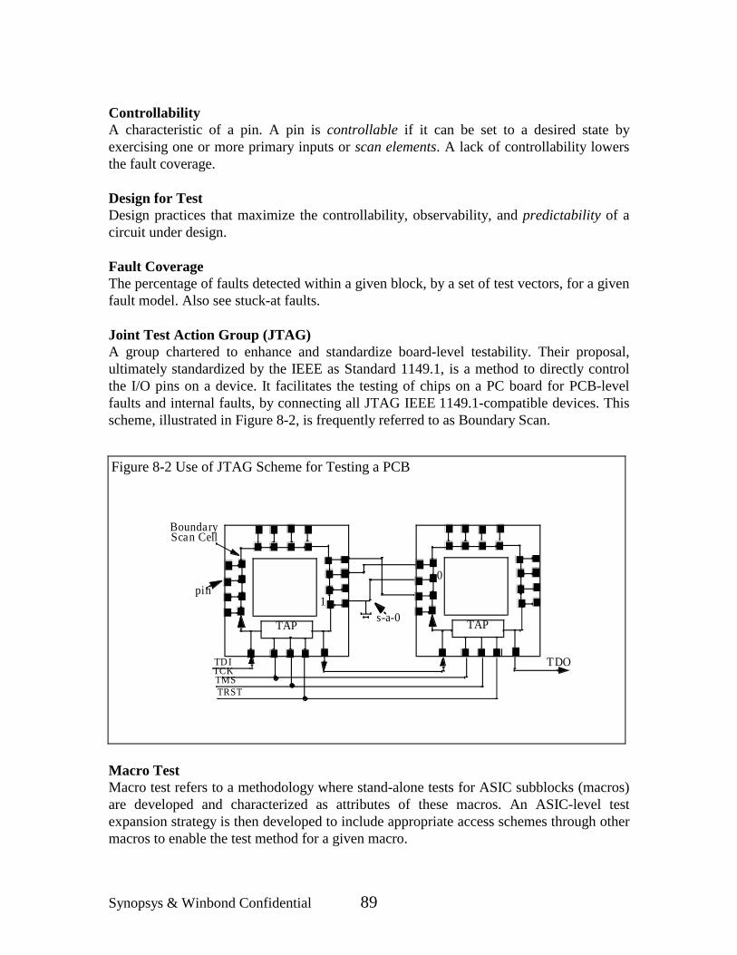
Synopsys & Winbond Confidential 89
ControllabilityA characteristic of a pin. A pin is controllable if it can be set to a desired state byexercising one or more primary inputs or scan elements. A lack of controllability lowersthe fault coverage.
Design for TestDesign practices that maximize the controllability, observability, and predictability of acircuit under design.
Fault CoverageThe percentage of faults detected within a given block, by a set of test vectors, for a givenfault model. Also see stuck-at faults.
Joint Test Action Group (JTAG)A group chartered to enhance and standardize board-level testability. Their proposal,ultimately standardized by the IEEE as Standard 1149.1, is a method to directly controlthe I/O pins on a device. It facilitates the testing of chips on a PC board for PCB-levelfaults and internal faults, by connecting all JTAG IEEE 1149.1-compatible devices. Thisscheme, illustrated in Figure 8-2, is frequently referred to as Boundary Scan.
Macro TestMacro test refers to a methodology where stand-alone tests for ASIC subblocks (macros)are developed and characterized as attributes of these macros. An ASIC-level testexpansion strategy is then developed to include appropriate access schemes through othermacros to enable the test method for a given macro.
Figure 8-2 Use of JTAG Scheme for Testing a PCB
TAP
TD ITCKTMSTRST
TDO
pin
BoundaryScan Cell
s-a-01
TAP
0
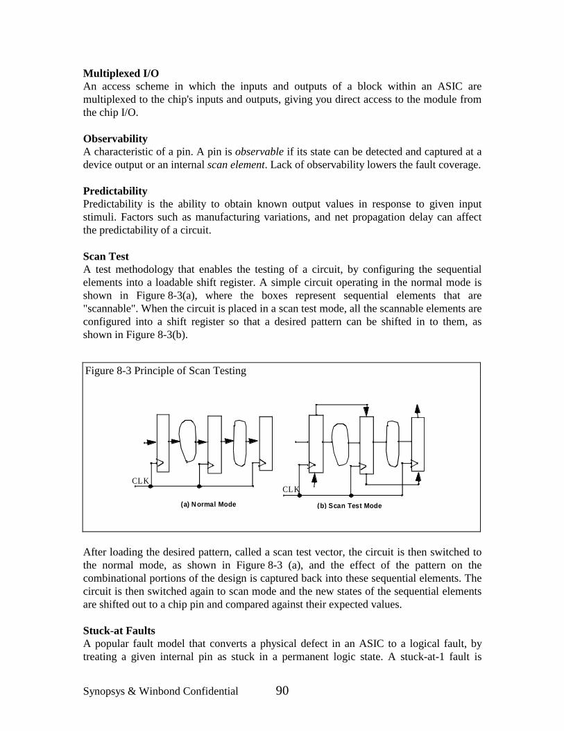
Synopsys & Winbond Confidential 90
Multiplexed I/OAn access scheme in which the inputs and outputs of a block within an ASIC aremultiplexed to the chip's inputs and outputs, giving you direct access to the module fromthe chip I/O.
ObservabilityA characteristic of a pin. A pin is observable if its state can be detected and captured at adevice output or an internal scan element. Lack of observability lowers the fault coverage.
PredictabilityPredictability is the ability to obtain known output values in response to given inputstimuli. Factors such as manufacturing variations, and net propagation delay can affectthe predictability of a circuit.
Scan TestA test methodology that enables the testing of a circuit, by configuring the sequentialelements into a loadable shift register. A simple circuit operating in the normal mode isshown in Figure 8-3(a), where the boxes represent sequential elements that are"scannable". When the circuit is placed in a scan test mode, all the scannable elements areconfigured into a shift register so that a desired pattern can be shifted in to them, asshown in Figure 8-3(b).
After loading the desired pattern, called a scan test vector, the circuit is then switched tothe normal mode, as shown in Figure 8-3 (a), and the effect of the pattern on thecombinational portions of the design is captured back into these sequential elements. Thecircuit is then switched again to scan mode and the new states of the sequential elementsare shifted out to a chip pin and compared against their expected values.
Stuck-at FaultsA popular fault model that converts a physical defect in an ASIC to a logical fault, bytreating a given internal pin as stuck in a permanent logic state. A stuck-at-1 fault is
Figure 8-3 Principle of Scan Testing
(a) N ormal Mode (b) Scan Test Mode
CLKCLK

Synopsys & Winbond Confidential 91
permanently high. A stuck-at-0 fault is permanently low. Fault types cannot be changedwithin a set of test patterns.
Test PatternA series of logic values (0, 1, x, z) applied to inputs and corresponding logic valuesexpected at the outputs during a test cycle period.
8.2.2 Fault Model
Fabrication defects are not directly attributable to human error. Rather, they result froman imperfect manufacturing process and result in breaks and shorts in interconnectingwires, improper doping profiles, mask alignment errors, and poor encapsulation. Theprobability that a device will malfunction due to a particular defect introduced by thefabrication process is a function of various factors such as the feature size, die size, andthe number of fabrication layers. Accurate identification of the source of fabricationdefects is critical to improving the manufacturing yield. It is desirable to model the effectof a physical defect as an effect on the logical behavior of the circuit. However,fabrication defects and other physical failures due to aging, operating conditions and soon are not amenable to direct modeling techniques. Instead, they are handled byrepresenting the effect of physical defects on the logical operation of a device. The basicassumptions regarding the nature of logical faults are referred to as a fault model. Thereare several fault models such as stuck-at faults, stuck-open faults, and bridge faults (alsoknown as stuck-to-neighbor faults). However, the most widely used fault model is that ofa single pin, or interconnecting wire, being permanently stuck at a logic value. The stuck-at fault model is popular because of its simplicity and effectiveness in modeling physicaldefects such as shorts and opens in CMOS technology as logical faults. The methodologypresented in this chapter predominantly uses the stuck-at fault model.
8.2.3 Fault Coverage
The test generation software creates a list of all possible faults in the ASIC, based on a setof fault models, for example, stuck-at-faults, open faults, bridge-faults. For a given set offaults in the design, you can determine the actual fault coverage, using several methods:
� Estimation: There are statistical estimation methods that develop a small set oftest vectors for a given circuit, compute the fault coverage achieved by these testvectors, and extrapolate the fault coverage achievable with a complete set of testvectors. Some test generation tools can estimate the fault coverage, based on thetest methods selected, for example, scan testing. However, this estimate may notbe accurate. For example, using a partial scan methodology where the scanmethod is applied to a fraction of the sequential elements of an ASIC, theachievable fault coverage may not be related to the fraction of the sequentialelements that are made scannable. Furthermore, there are faults whose effects
Synopsys & Winbond Confidential 92
cannot be predicted. For instance, many test generation tools cannot predict thestate of a three-state net if multiple drivers cause a signal collision on this net.
� Fault Simulation: In this method, test patterns generated manually or through anATPG to cover all the faults, for example, stuck-at-0, and stuck-at-1, are appliedto the circuit and the differences between the actual and expected responses areused to determine the actual faults detected.
� Deriving from test scheme: For some special structures, the exact fault coveragecan be obtained prior to the test scheme employed, for example, Built-in Self-Test for memory arrays.
8.2.4 Fault Detection
The detection of a fault can be done by patterns produced from executing ATPGalgorithms. For each stuck-at fault in the circuit, an ATPG algorithm attempts todetermine the following:
� A path to propagate the effect of a given fault to an observable output of thecircuit, that is, create a difference in an output value between good or faultycircuits
� The actual values to be assigned to the primary inputs of the circuit to"sensitize" this path for the propagation of the given fault to the output
There are two major categories of ATPG algorithms - combinational and sequential. Thelatter is more complex because of the need to propagate the effect of a fault throughsequential logic, requiring multiple clock cycles. The successful completion of an ATPGalgorithm for a given fault depends on the type of fault, the distance (number of levels oflogic) from the faulty pin to the primary inputs and outputs, the structure of the circuit,and the nature of the sequential logic. These factors are explained in the next section.
8.2.5 Untested Faults
Some faults might not be tested by a test generation tool for several reasons. The mostcommon reasons are:
� Design rule violations such as combinational feedback loops and gated clocks� Cells modeled as black boxes, with functionality unknown to ATPG� Pins held at some logic states, for testing some faults or due to unused logic� Unpredictability of certain faults, for example, tri-state bus collision� Reconvergent Fanout
If the test program holds an internal pin in a fixed state in order to test other circuits, thenthis pin is not tested for the corresponding stuck-fault.

Synopsys & Winbond Confidential 93
Reconvergent fanout refers to the structure of a circuit where different paths from thesame signal pin converge again at the same component, downstream in the logic.Reconvergent fanout can affect the fault coverage of a circuit. While reconvergent fanoutdoes not necessarily make a circuit untestable, it can complicate the problem of testgeneration and diagnosis. Specifically, the task of computing a test vector to detect agiven fault in a circuit with reconvergent fanout may have to extend beyond thetraditional tree-search algorithms. Note that the normal boolean optimization performedby synthesis tools should eliminate any reconvergent fanout within a block. Therefore,test generation tools, generally, do not have to handle reconvergent fanout. However,there are a couple of mechanisms that can potentially introduce reconvergent fanout into adesign. First, certain synthesis optimization constraints, for example, componentinstantiation and/or the use of the set_dont_touch attribute, may inhibit theelimination of reconvergent fanout. Secondly, improper partitioning of combinationallogic into different ASIC subblocks may lead to reconvergent fanout across subblocks, asshown in Figure 8-4.
Consider a stuck-at-0 fault on the output of gate U1 in Module A. If the fault propagationalgorithm chooses to propagate this fault through gate U3 of Module B, (as indicated by aD on the lower input to gate U3), it will require input I1 to be 1. But I1=1, through gatesU2 and U4, will "mask" out the propagation of the fault through the final gate U5 ofModule B.Recommended synthesis partitioning guidelines, for example, not partitioningcombinational logic across blocks, should eliminate most of these situations.
8.3 Test Schemes
This section discusses several popular test schemes and the recommendations regardingtheir application. In particular, the operation of each scheme, its implementation,advantages and side-effects are discussed. Finally, guidelines for the selection ofappropriate test schemes are presented.
Figure 8-4 Reconvergent Fanout Due to Poor Circuit Partitioning
A B
U1
U2
U3
U4U5
10
s-at-0D_
D?_D
1I1

Synopsys & Winbond Confidential 94
A test scheme for a circuit, in the context of this chapter, refers to the hardware structureand the protocols necessary for testing a given circuit. Adhering to the testability rulesdiscussed above will greatly facilitate the process of inserting suitable test structures andgenerating the test vectors to achieve the desired fault coverage.This section discusses thenext major step in the test methodology after testability analysis, namely selecting andimplementing appropriate test schemes. In particular, internal scan test, boundary scan,built-in self-test for RAMs, and special methods for embedded core cells are covered. Ageneral caveat applies to any test scheme: the test structure itself must be testable. Youshould keep in mind the importance of the modeling of the technology library so that thetest generation software can derive the testability attributes of cells. For instance,providing the functional equivalent of an embedded macro simplifies its testing. However,modeling a technology library for test is the responsibility of the semiconductor vendorand is beyond the scope of this document.
8.3.1 Scan Test Methodology
The scan method of testing solves the inherent accessibility problem of sequential logicwhich may require many clocks to reach a certain desired state during normal operation.For example, a finite state machine may drive a primary output only in one of its states.However, to get the state machine into this state in order to verify its proper operation, itmay take several clocks and several primary input combinations. A scan schemecircumvents this problem by directly loading the sequential elements by shifting thedesired values into them. A scan test scheme operates by serially shifting in a desiredpattern directly into the sequential devices of a design independent of its normal inputs,stimulating the combinational logic with this pattern, capturing the response of thecombinational logic back into these sequential elements, and examining these new valuesby serially shifting them out to an output pin.
8.3.1.1 Full Scan Methodology
In the full-scan design technique, all sequential cells in your design are modified toperform a serial shift function. Sequential elements that are not scanned are treated asblack box cells (cells with unknown function).
Full scan divides a sequential design into combinational blocks as shown in Figure 8-5.Ovals represent combinational logic; rectangles represent sequential logic. The full-scandiagram shows the scan path through the design.

Synopsys & Winbond Confidential 95
Through pseudo-primary inputs, the scan path enables direct control of inputs to allcombinational blocks. Through pseudo-primary outputs, the scan path enables directobservability of outputs from all combinational blocks. You can use efficientcombinational ATPG algorithms to achieve high fault coverage results on the full-scandesign.
8.3.1.2 Partial Scan Methodology
In the partial-scan design technique, the scan chains contain some, but not all, of thesequential cells in your design. The partial-scan technique offers a tradeoff between themaximum achievable fault coverage and the effect on design size and performance.
Partial scan divides a complex sequential design into simpler sequential blocks as shownin Figure 8-6. Ovals represent combinational logic; rectangles represent sequential logic.The partial-scan diagram shows the scan path through the design.
Figure 8-5 Scan Path through a Full-Scan Design

Synopsys & Winbond Confidential 96
Use sequential ATPG algorithms on your partial-scan design to allow fault propagationthrough nonscan sequential elements. In general, a partial-scan design cannot achievefault coverage as high as a full-scan design can. The level of fault coverage for a partial-scan design is related to the location and fraction of scan registers in that design.
Sequential ATPG algorithms are slower than combinational ATPG algorithms, and theyuse more memory.
8.3.2 Boundary Scan
Boundary scan is a test technique devised to automate PCB-level testing by providing achip-board test interface. In this method, a device to be tested is supplemented with logicto propagate test vectors between pins and the core of the device. IEEE has formalized itsspecification as the IEEE 1149.1-1990 standard. This technique is also referred to as theJTAG (Joint Test Action Group) scheme due to the source of its original proposal. Someboard-level testability tools require that the ASIC vendors' boundary scan implementationbe represented in VHDL or BSDL (Boundary Scan Description Language). Boundaryscan addresses board-level issues and does not fully address chip-level testability. Youcan combine chip-level techniques such as internal scan with boundary scan to covertestability at both the board and chip levels. Providing separate internal scan chain andJTAG boundary scan chain can reduce manufacturing test time and promote parallelmultiple chain operation.
8.3.2.1 Basic Principle of Boundary Scan
Implementing boundary scan inserts small amounts of logic, called Boundary ScanRegister cells, between each pin and the chip circuitry to which that pin is normally
Figure 8-6 Scan Path through a Partial-Scan Design

Synopsys & Winbond Confidential 97
connected, as shown in Figure 8-7. In addition to their connections to the package pinsand the internal core logic of the ASIC, the boundary-scan cells have other terminalsthrough which they can be connected to each other, forming a shift register around theperiphery of the ASIC.
The structure of the Boundary Scan Register is shown in Figure 8-7(b). During normaloperation, the boundary cells act transparent and connect the device pins directly to theinternal core logic. When put in the test mode, however, they can be connected to otherASIC pins as a shift register. Thus, a test program can serially shift in a desired value intothe Boundary Scan Register cells. The mode of operation of the Boundary Scan Registercells can then be switched such that the data loaded into them are used either to drive theinternal core logic or to drive the ASIC pins, regardless of the internal core logic. Theshift register path need not be confined to a single chip, but can encompass the entirePCB, as illustrated in Figure 8-7(a). This makes it possible to test either the internal logicor external chip-to-chip connections. In particular, JTAG makes it possible to test forerrors in wire-bonding between internal pads and the package pins, chip soldering defects,and PCB trace opens and shorts, as illustrated in Figure 8-7. The extent of such testing isdetermined by the number of devices that are equipped with JTAG logic. Devices withoutJTAG will require traditional test methods such as bed-of-nails fixtures for testing thePCB-level faults.
Figure 8-7 Operation of Boundary Scan
TMSTRST
TDO
cellTo next
Fromprevious
cell
Internal logicInput pin
(b) Boundary Scan Register
(a) Connecting Devices with Boundary Scan
TDI
U1 U2
TCK
Internal logic Output pin
TAP TAP
PCBfault
1
0Pin
BSRcell

Synopsys & Winbond Confidential 98
8.3.2.2 Components of Boundary Scan
Figure 8-8 shows the conceptual organization of a boundary scan scheme.
The 1149.1 interface consists of the following components:
� TAP (Four or five pin Test Access Port)� TMS (Test Mode Select)� TCK (Test Clock pin)� TDI (Test Data In pin)� TDO (Test Data Out pin)� TRST (Optional Asynchronous Test Reset pin)
The TRST pin is not mandatory as explained later in this section. However, resetting theJTAG logic without this pin may fail under various conditions, for example, 3-valuesimulator and default initialization protocols for scan, which do not use this feature.Therefore providing a separate TRST pin is highly recommended.
Boundary scan as specified by 1149.1 JTAG consists of the following components:
� TAP Controller� Instruction Register� Data Registers
The TAP controller controls the operation of the boundary scan test logic by generatingthe clock and control signals used by the test data and instruction registers. State
Figure 8-8 Boundary Scan Scheme
Bypass
TCK
RegInstr
TDO
BSR
Reg Decode
TDI

Synopsys & Winbond Confidential 99
transitions within the TAP Controller are determined by the value of TMS and occur onthe rising edge of TCK. The TAP controller resets to the Test-Logic-Reset state in one oftwo ways:
� By setting the asynchronous reset signal, TRST* (if your design uses thisoptional signal)
� By clocking five cycles with TMS held at a logic 1.
Boundary scan circuitry operates according to instructions that are serially shifted into theinstruction register from TDI. The JTAG standard requires certain instructions andsupports user-defined instructions. Each instruction selects a data register to be connectedbetween TDI and TDO. The instruction register must be at least two bits wide toaccomodate the following mandatory boundary scan instructions required by the IEEEstandard:
� BYPASS� SAMPLE/PRELOAD� EXTEST� IDCODE (if your design includes a Device Identification register)
The Decode block interprets the instruction loaded in the Instruction Register, selects aparticular data register to be connected to TDO, and controls the mode of operation ofthis data register.
In the boundary scan method, the TAP Controller uses Data Registers as the mechanismto transfer test data into or out of the chip. One data register can be addressed through theTAP at a time. The Data Register mechanism is also used to access other test structures inthe internal logic, such as internal scan chain, BIST register and so on. The different typesof data registers are:
� Boundary Scan Register (BSR)� Bypass Register� Device Identification Register (optional)� User-Defined Data Registers (optional)
Most Boundary Scan Registers in the boundary scan logic and the Instruction Register areconstructed with dual ranks; a shift register flip-flop and a latch flip-flop as shown inFigure 8-9.

Synopsys & Winbond Confidential 100
The clocks to these two flip-flops are controlled by the state of the TAP controller. Thisdual-rank construction prevents the rippling data during the shifting operation from beingvisible to downstream logic. The final mux in the Boundary Scan Register cell introducesan additional delay in the signal path. If a signal is speed-critical or if the time-budget fora signal cannot accomodate any additional delay, you can eliminate the Latch Flip-flopand the final mux in the Boundary Scan Register cells. The configuration of the BoundaryScan Register in the various modes of operation are shown in Figure 8-10.
The connections within the Boundary Scan Register cell in the Normal Mode, in (a)above, makes the cell logic transparent. In the Test Mode, shown in (b), the data held inthe Hold Latch of the cell is propagated to the DataOut pin which drives the internal corelogic or the ASIC output pin. In the Serial Scan Mode, all BSR cells are connected as ashift register. In the Update Mode, the data in the shift register flip-flop is loaded into theHold flip-flop of the BSR cell.Each port, or pad, of the design has at least one boundary scan register cell associatedwith it. A simple input port can have a single Boundary Scan input cell. A two-stateoutput port can also have one Boundary Scan cell associated with it. A three-state outputcan have two Boundary Scan cells, an output cell and a control cell, associated with it. Abidirectional port can have three Boundary Scan cells associated with it; input, output,and control cells.
Figure 8-9 Typical Boundary Scan Register Cell in Boundary Scan
TMSTRST
TDO
Shift/Load
Update
cellTo next
Fromprevious
cell
Internal logicInput pin
Mode
TDITCK
Shift
Shif tReg LatchFlip-flop Flip-flop
Capture/
Internal logicOutput pin
TAP
FinalMux

Synopsys & Winbond Confidential 101
8.3.3 Techniques for Testing Embedded RAMs
The test methodology of Figure 8-11 included the implementation of test methods forembedded RAMs in the same step as internal scan chains. RAMs usually require specialtesting approaches quite different from less structured and less compact logic circuits. Itis straightforward to generate test patterns for embedded memory arrays to completelyand exhaustively achieve full fault coverage. The logic connected to an internal memoryarray can thus be tested by exercising the memory array "in place". However, it is muchmore efficient to separate the testing of memory arrays and the rest of the ASIC. There
Figure 8-10 Configurations of Boundary Scan Register
Shift/Load
UpdateShiftInMode
Shift
Shif tF/F
Capture/
(a) Normal Mode
(b) Test Mode
DataIn DataOut
(d) Update Mode
(c) Serial Scan Mode
Hold F/F
Shift/Load
Update
ShiftOut
ShiftInMode
Shift
ShiftF/F
Capture/
DataIn DataOutHold F/F
Shift/Load
Update
ShiftOut
ShiftInMode
Shift
ShiftF/F
Capture/
DataIn DataOutHold F/F
Shift/Load
Update
ShiftOut
ShiftInMode
Shift
ShiftF/F
Capture/
DataIn DataOutHold F/F

Synopsys & Winbond Confidential 102
are two major reasons for this separation:
� Partitioning the ASIC into memory arrays and other logic permits appropriatetest algorithms for each: pattern-sensitive faults for memory and ATPG for logic.
� Fault models used for conventional logic circuits, for example, stuck-at faults,are not applicable to memory arrays. Memory arrays tend to exhibit differentbehavior in the presence of manufacturing defects, for example, stuck-to-neighbor, or data retention. Although the defects in regular structures such asmemory arays are well-known, there are few popular methods for modelingthese defects as logical faults. Therefore, the rest of the ASIC may have to betested without including the memory blocks.
This separation of memory arrays from the rest of the ASIC for test purposes can beaccomplished through two mechanisms:
1) Providing direct access to the RAM ports from chip-level pins or scan chainelements, and2) Bypassing the memory arrays for test purposes.
This section describes methods to isolate and test the rest of the ASIC independent ofmemory arrays. Use of BIST methods for testing memory arrays is introduced later.
8.3.3.1 Multiplexed I/O Scheme for Bypassing Embedded RAMs
The simplest solution to bypass embedded RAMs is to incorporate multiplexers to bypassthe RAM ports in the test mode. This isolation circuitry can serve two purposes:
� Increase the observability of the logic driving the RAM� Increase the controllability of the logic connected to the RAM
If the RAM has a known state during test operation, controllability of the RAM outputs isnot required. Figure 8-11 illustrates the multiplexer scheme for RAM isolation.
In the design above, multiplexer M1 selects between the RAM input data and the RAMoutput data. Therefore, in the RAMTest mode, instead of the uncontrollable RAM outputdata, controllable input data is propagated further into the design for observation at theASIC pins. Similarly, multiplexer M2 selects between the normal address bus to theRAM and other internal signals. This mux increases the observability of the addressdriving the RAM by enabling it to an observable output.
If the address bus to an embedded RAM is driven directly by an internal register withoutany intervening combinational logic, then multiplexer M2 is not necessary. Instead, theaddress register can be connected as part of an internal scan chain for full controllabilityand observability, as discussed further in the next section.

Synopsys & Winbond Confidential 103
A RAM typically has more inputs than outputs and therefore, often the address linesneed to be muxed with other functional pins during test to make those signals controllable.However, it is not recommended for memory buses more than 16 bits wide because of therouting congestion around the memory.
Note that the RAM is not functionally modeled in this method and therefore is not testedeven for faults on its ports. Therefore, faults with respect to the RAM block pins shouldbe excluded from the fault list in this case. For example, with Test Compiler, this is doneby using the test_dont_fault directive. If you use this method to isolate the RAM, youmust develop an independent method for testing the RAM.
8.3.3.2 Multiplexed RAM Pins at Device I/O
A simple method to test embedded RAMs is to make all the RAM pins accessible atdevice pins. This approach would allow the exhaustive testing of the RAM. However,this method is limited to small RAM arrays due to the complexity of multiplexing theRAM signals to the device pins.
8.3.3.3 Boundary Scan Method for RAMs
Another approach for testing the logic around an embedded RAM, as well as accessingthe RAM array itself, is to create an independent scan scheme around the RAM. In thismethod, known as the Register Bounding scheme, scan register cells are placed aroundthe memory address and data busses, as shown in Figure 8-12. Multiplexers are added toselect between the RAM I/O and the scan chains for the rest of the ASIC. In the normal
Figure 8-11 Mux Isolation Technique for Achieving High Testability for Logic AroundRAM
RAMTest
ID0
AD0
D0
inputs
Normal 1
0
1
0
pins or
RAM
ComboLogic
M1
M2
scan F/F

Synopsys & Winbond Confidential 104
mode, the bounding registers in the RAM paths are bypassed.
The rest of the ASIC is isolated from the memory array by the bounding registers and canbe tested independently. The bounding registers can be used to directly access the RAMarray for memory testing. During memory test, the scan cells for the rest of the ASIC areignored. All memory arrays to be tested are generally connected into one scan chain. Thismethod is not appropriate for memory arrays more than 1K words in view of the test timefor test vector serialization. Similar to the multiplexed I/O scheme of the previous section,the additional scan registers and multiplexers are necessary in the Register Boundingscheme only if there is combinational logic between the address/data registers and thepins of the RAM. It should be noted that the Write_Enable pin of the RAM may have tobe treated as a special case when it is controlled through scan registers. This is becauseunintended edges on this signal may write spurious data into the RAM during scan shift.To avoid this problem, you can gate the Write_Enable signal with the ScanEnable signal.
8.3.3.4 A structural Model for RAMs
A more complex approach for testing the logic around an embedded RAM is to build astructural equivalent model for the RAM. This scheme will enable the RAM to beinitialized to a known state so that the rest of the ASIC can be tested using sequentialATPG algorithms. In particular, the RAM can be modeled for any desired data so thatother blocks outside the RAM can be exercised with specific RAM data patterns. Thismethod is generally not recommended due to its difficulty of implementation and shouldonly be considered for small memory arrays, less than 128 words. Note that this methoddoes not test the RAM array itself.
8.3.3.5 Transparent RAM Mode
Figure 8-12 boundary Scan Technique for Embedded RAMs
RAM
Logic Test Path RAM Test Path Logic Test Path
BoundingRegisters
ComboLogic
ComboLogic
TestMode
Functional Path
CLK

Synopsys & Winbond Confidential 105
Another test option for the logic around an embedded RAM is to use the RAM in atransparent mode of operation. This mode has to be defined in the library used by the testgeneration tool. Using the initialization test protocol, configure the RAM in thistransparent mode. Make sure that the RAM is held in the transparent mode throughout thetest cycle. This technique also does not test the RAM array itself.
8.3.3.6 Built-in Self Test (BIST)
BIST is applicable to any functional block with reasonably good structure and iscommonly used for the automatic testing of RAM arrays. This technique requiresadditional control circuitry surrounding the RAM for exercising it with different addressand data patterns, analyzing the response, and reporting the results. The additional realestate required for this is generally worth the investment, especially for RAM/ROMarrays larger than 8Kb.
A BIST generation tool can automatically insert the BIST controller and a RAM interface,known as a BIST collar. As described under the previous "Boundary Scan", the TAP portcan enable a BIST controller through the RUNBIST instruction. The BIST controller will,in turn, apply a series of pre-determined address and data patterns serially through theBIST collar, as illustrated in Figure 8-13. The collar will then write data into the RAMarray in parallel and read it back in parallel at normal speed. Multiple memory blocks canbe handled by a single BIST controller.
A BIST method offers several benefits in testing memory arrays:
� Low area overhead: about 400 gates for the simple "Walking 1/0" test and
Figure 8-13 Built-in Self Test for RAM
TAP
ADDRDOUT
Ser DataInBIST
Memory Data OutDataIn
BISTAddr
godone
bist BIST
BISTSerDataOut
BIST
MemAddr
Cntrl
Mem
Mem Cntrl RAM
CNTRL
BIST Collar
DIN
Controller

Synopsys & Winbond Confidential 106
almost independent of memory size� Simple Test Pattern generation: with BIST, the designer does not need to
develop detailed memory test patterns, but only the test instruction that triggersthe BIST controller and monitors the status bit
As discussed above, the BIST scheme introduces an additional mux delay to the memorypath, within the BIST collar. Contact your semiconducor vendor to determine the use andcontrol of this mux in compiled memory arrays. A BIST method for memory testing hasto be complemented with other test methods, such as scan chain, for the logic surroundingembedded RAMs.
8.3.4 Testing Embedded Cores
Embedded cores, also referred to as macros, pose unique challenges to ASIC validationand test. These issues become more formidable if the project goals require that the ASICbe silicon-foundry independent. There are two major categories of macros:
� Hard macros which are pre-synthesized and have a physical implementationwith a well-defined bounding box,
� Soft macros which are gate-level netlists that can be combined with other blockswithin the ASIC for placement and routing.
8.3.4.1 Defining Test Methods for Embedded Cores
It should be noted that there are no industry standards for testing embedded cores andeach silicon vendor has some proprietary method for testing macros. Similar to internalRAM blocks, testing a macro requires a mechanism for propagating the stimulus from thechip boundary to the macro boundary and the macro�s response to the chip pins.Therefore, the schemes described earlier for memory arrays can be extended to embeddedcores. However, it is more complex to model the functionality of a macro within the restof the ASIC. It is necessary to implement methods to independently test the macrowithout any influence from the rest of the ASIC. Therefore, the following issues need tobe addressed early in the design cycle:
1) What is the protocol for initializing the macro and testing it for functionality andtiming? This will determine how the macro is tested independent of the other ASICblocks.2) In the case of a hard macro, is the macro supplied as a functional black box inorder to protect the intellectual property? If so, there may be no way to propagatestimuli or responses either through or around the macro.3) An additional complication in validating soft macros is that the layout-dependenttiming attributes of the macros are not known prior and so the ASIC may need to bereoptimized after layout to satisfy the macro timing.

Synopsys & Winbond Confidential 107
If a macro is a functional black box, it will prohibit the development of structural testpatterns. Some macro vendors provide functional equivalent models for the macros fortestability purposes. The functional equivalent model for the macro is replaced by itsstructural black box version by the vendor after the sign-off step. In the case of a blackbox macro, the Test Generation tools should be instructed to exclude faults associatedwith the pins of the black box from the fault list.
8.3.4.2 Selecting Test Methods for Embedded Cores
There are some global issues that affect the selection of a test methodology for macros:
� Linking test methods for various macros and other blocks within the ASIC� Developing clocking methodologies to cope with clock skew and uncertainty
The core vendor may not always provide a set of tests for embedded cores. Even whentest vectors are supplied, the requirements at the boundary of the core for using these testvectors have to be evaluated in the context of the ASIC under design. For instance, a setof test vectors for a macro may have been developed under the assumption that it ispossible to provide a clock to the macro as each vector is applied, but this may not bepossible due to the way the macro's clock port is connected in a given ASIC. Therefore,you should investigate the applicability of a test vector suite from the macro vendor to theenvironment for the macro within your ASIC.
A methodology to arrive at the optimum test scheme for embedded macros is presentedbelow. It is a function of the test scheme built-in by its vendor, as well as the ease ofdirect access to the macro from the ASIC pins.
� Possible to have direct access to the macro: A structural version of the macro isavailable. This is the simplest method of testing the core although it requiresmultiplexing the core's ports to the device pins. These multiplexers can beenabled by a special test mode signal.
� Full pin access to the macro prohibitive, but the macro has internal scan chain:Here again, the structural version of the macro is available. The vendor shouldsupply test vectors suitable for scan tesing the macro through its pins. Use oneof the following methods for accessing the scan chain within the macro.
If possible, provide a direct scan access to the macro by multiplexing its ports to thedevice pins. Thus, the macro can be scan-tested independent of the rest of the ASIC.This will eliminate the need to merge the scan test vectors supplied by the vendorwith other scan vectors for the rest of the ASIC, thereby permitting parallel scanchains. A macro with multiple internal scan chains requires additional ports.
Combine the scan chain(s) for the core with the scan chain(s) for the rest of theASIC. This involves merging the scan test vectors and possibly longer test time. Amacro with multiple internal scan chains requires merging their scan test patterns

Synopsys & Winbond Confidential 108
with those of the scan chains in the rest of the ASIC.
� Macro provided as a Black Box only with no logical circuit equivalent: Thisrequires that the macro be accessible through the ASIC pins. The vendor mayprovide a functional equivalent for the macro strictly for functional simulation.Note that you need to instruct the test generation tool to exclude the macro fromthe fault coverage. The macro can be enabled in one of the test modes and testedindependent of the rest of the ASIC.
8.3.5 MACRO Test Methodolody
Macro test methodology approaches the task of testing an ASIC by partitioning it into twolevels: leaf macro-level and device-level. A leaf macro is the basic subblock,characterized functionally in terms of its testability. Macro testing should bedistinguished from testing embedded macros discussed above. The macro testmethodology consists of a two-step approach to the testing of an ASIC:
� Developing an appropriate test method to satisfy the testability of each leafmacro, that is, testing its internal logic
� Preserving the controllability and observability of each leaf macro at the devicelevel, by finding appropriate access methods to exercise the test method for amacro from/to the ASIC pins. Conveying test vectors from/to the device pinsmay require placing other intervening macros in suitable modes for test vectorpropagation
The concept of macro testing is illustrated in Figure 8-14, which shows an ASIC withmacro blocks A, B, C, and M. These attributes for each macro are shown in italics.Macros M and C have been characterized for a scan chain test method both for internallogic and for propagating test vectors, Macro A has been enhanced with boundary scanfor both and Macro B has BIST for internal logic and transparent mode for propagation.
Figure 8-14 Concept of Macro Testing
A
ScanChain
B
Scan
ScanChain
Transparent
CM

Synopsys & Winbond Confidential 109
Therefore to test Macro M, the ASIC-level test strategy needs to set up access pathsbetween the ASIC pins and Macro M. This can be accomplished by using the accessattribute of other intervening macros as follows:
� Place Macro A in the boundary scan method so that the ScanIn data can bepropagated through it
� Place Macro B in a transparent mode to enable ScanEnable signal on to MacroM
� Place Macro C in the internal scan chain mode� Apply scan test vectors to Macro M by shifting in the desired data through the
boundary scan registers of A� Capture the new values into the sequential elements during its capture operation
and shift them out to a device pin by passing through the internal scan chain ofMacro C
In the macro test methodology, you may have to enhance the design to effectively makeeach leaf macro controllable and observable from the device pins. These enhancementsmay consist of additional structures that enable the access to the leaf macros. For instancein Figure 8-14, leaf macro B is controllable, but not directly observable at the device pins.Therefore, a BIST scheme has been added to obviate the observability requirement.
Since the device-level test plan in macro testing can control the routing order of macrosfor test vector propagation, this approach offers additional flexibility in selecting theoptimum macro ordering to access a given macro. For instance, if there are severalpossible scan chain paths through different leaf macros in a design, you can choose therouting order that minimizes the amount of test vector propagation in reaching its pins.
A successful macro test approach requires the development of the following :
� An intra-test method for each leaf-macro, for testing its internal logic� An inter-test mechanism to propagate test vectors to each leaf macro to/from
device pins
This approach can be effective in partitioning the task of testing complex ASICs withlarge gate counts and/or heterogeneous leaf modules, for example, RAMs, embeddedcores, structured logic, and random logic blocks. To satisfy the inter-test mechanismrequirement, you may have to insert additional structures in the design, such as muxes,transparent mode of operation, and bounding registers. You must specify the intra-testand inter-test macro-test attributes for each macro in order to obtain the most effectiveresults and early feedback on testability problems.
8.4 Design Rules
This section presents a set of recommended design rules that improve the testability of an
Synopsys & Winbond Confidential 110
ASIC. The previous section discussed specific test methods such as scan chain, boundaryscan, and test schemes for embedded macros.
A design rule is a recommendation regarding implementation of a circuit function. Thereis a well-accepted set of design practices that significantly improve the testability of anASIC. In other words, strict conformance to these design practices has been shown toreduce the number of testability problems and their impact. These design rules aretherefore known as testability rules. These design practices not only satisfymanufacturing testability requirements, but also improve the reliable operation of anASIC within the normal operating environment range in its target system. If a design istargeted to have high fault coverage, design rules are extremely important. One of themost important aspects of a design specification is the set of design rules.
It is important to keep in mind the following factors that affect testability:
� Sequential logic is much more difficult to test than combinational logic.� Control logic is more difficult to test than datapath elements.� Random logic is more difficult to test than structured circuits.� Asynchronous circuits or those with unconstrained timing signals are much
more difficult to test than synchronous circuits that have easily controllablesignal generation and distribution.
Conforming to strict synchronous and testable design styles simplifies the testing process.You may not be able to conform to these strict design rules in every situation. Forinstance, in some situations, you may choose to implement a partial scan scheme ratherthan full scan. During the design stage, carefully analyze the net cost of not implementinga design rule, before electing to violate the design rule.
8.4.1 Synchronous vs. Asynchronous Logic
The preferred way to implement sequential elements in an ASIC is a synchronousclocking scheme. Designs that violate this property, that is, asynchronous circuits, lead totwo major problems:
� They complicate the tasks of specifying the constraints for synthesis, test,simulation, and layout tools. For example, there is no mechanism to annotate aVHDL file to inform the synthesis tool that a particular input is valid onlyduring a particular set of states. Thus, you may have to hand-instantiate somegates to preserve input signal ordering. Furthermore, the layout of asynchronousblocks requires very careful placement due to their sensitivity to relative signaldelays.
� High-level design tools are built to handle a synchronous design style and, evenwith considerable effort, can only handle very limited asynchronous circuits. Forexample, gates used for the purpose of inserting delays may be removed by logic

Synopsys & Winbond Confidential 111
optimization and so you need to place a dont_touch synthesis attribute onthem. Furthermore, timing requirements for asynchronous circuits cannot beguaranteed with static timing analysis, but require full-timing simulation tocover the full spectrum of operating conditions.
Whenever possible, follow a synchronous design style and ensure that the clock signal forevery sequential element in the design can be controlled through the device pin(s). Inparticular, avoid one-shots, asynchronous state machines, and asynchronous signals thatare not demetastabilized and delay gates. Instantiation of timing-sensitive orasynchronous circuits was discussed in the previous chapter. If you must absolutely useasynchronous logic in your design, place asynchronous circuit in its own level ofhierarchy. In the design specification, outline the areas in the design that are notsynchronous or fully verifiable through other means. Within the specification, includespecial plans for these design areas during synthesis, gate-level simulation, and layout.
8.4.2 Internal Three-State Nets
Internal three-state signals can reduce reliability if the drivers for these signals are notcontrolled properly. When a fully decoded three-state bus switches owners, one drivergoes into high impedance at the same time that another driver starts driving. Because ofplacement, routing, and delays, a driver may begin driving before the previous driverreaches the high impedance state. This situation, called orthogonal drive, with drivers onthe same net driving different values (1 and 0), results in the pull-up transistor of onecircuit and the pull-down transistor of another being on at the same time. Even thoughthis may occur only for brief periods, it can reduce the life expectancy of the circuit due tothe increased power dissipation and the resultant elevated junction temperatures. Theorthogonal drive situation can be avoided in two ways:
� By providing a pull-up on the net and using open-drain drivers; this willeliminate a contention between active pull-ups and active pull-downs.
� By providing a pull-up on the net and ensuring that there is a "turnaround state"between successive drivers; this will prevent two simultaneous drivers and alsoguarantee a valid state at all times.
Most ASIC vendors discourage the use of internal three-state buses for the inherenttestability problem. It may be necessary to rely on current consumption during themanufacturing test to detect such faults on three-state nets.Even in situations where a cell has tri-state outputs, for example, RAM, convert thesesignals to regular (driven) signals by making the output enable a two-state signal, that is,by hardwiring the output enable signal to the active state.
8.4.3 Multiple Active Drivers on a Three-State Net
Exactly one drive must exist at all times on a three-state net. Figure 8-15 shows a three-
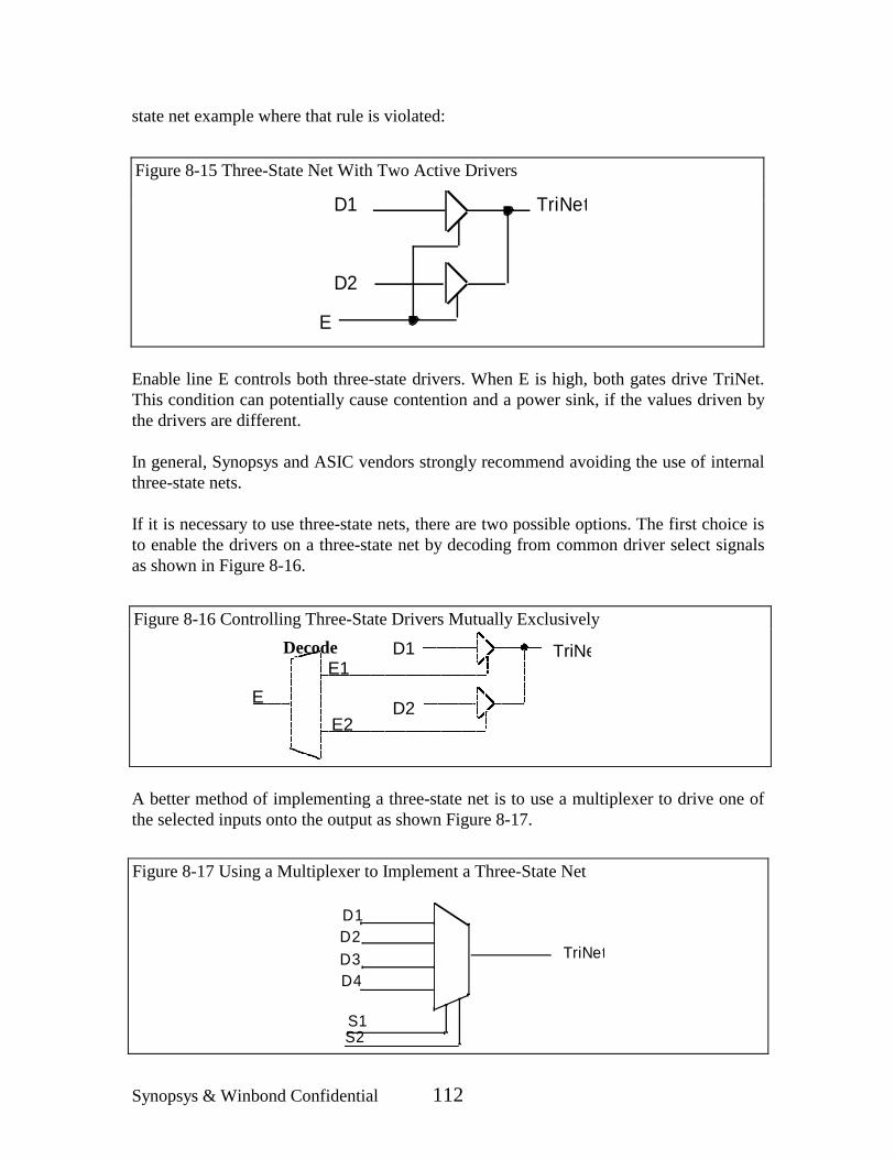
Synopsys & Winbond Confidential 112
state net example where that rule is violated:
Enable line E controls both three-state drivers. When E is high, both gates drive TriNet.This condition can potentially cause contention and a power sink, if the values driven bythe drivers are different.
In general, Synopsys and ASIC vendors strongly recommend avoiding the use of internalthree-state nets.
If it is necessary to use three-state nets, there are two possible options. The first choice isto enable the drivers on a three-state net by decoding from common driver select signalsas shown in Figure 8-16.
A better method of implementing a three-state net is to use a multiplexer to drive one ofthe selected inputs onto the output as shown Figure 8-17.
Figure 8-15 Three-State Net With Two Active Drivers
Figure 8-16 Controlling Three-State Drivers Mutually Exclusively
Figure 8-17 Using a Multiplexer to Implement a Three-State Net
D1
D2
E
TriNet
D1
D2
TriNeE1
E2E
Decode
TriNet
D1D2D3D4
S2S1
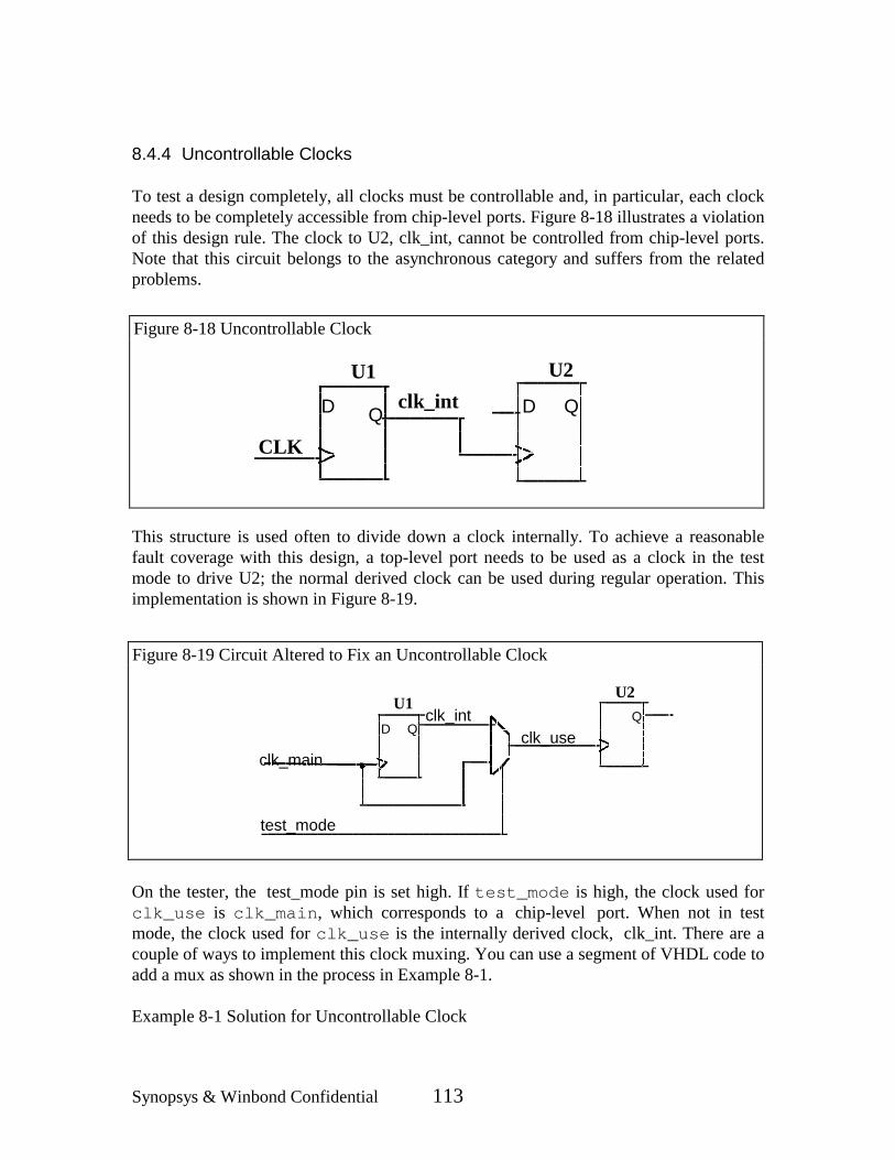
Synopsys & Winbond Confidential 113
8.4.4 Uncontrollable Clocks
To test a design completely, all clocks must be controllable and, in particular, each clockneeds to be completely accessible from chip-level ports. Figure 8-18 illustrates a violationof this design rule. The clock to U2, clk_int, cannot be controlled from chip-level ports.Note that this circuit belongs to the asynchronous category and suffers from the relatedproblems.
This structure is used often to divide down a clock internally. To achieve a reasonablefault coverage with this design, a top-level port needs to be used as a clock in the testmode to drive U2; the normal derived clock can be used during regular operation. Thisimplementation is shown in Figure 8-19.
On the tester, the test_mode pin is set high. If test_mode is high, the clock used forclk_use is clk_main, which corresponds to a chip-level port. When not in testmode, the clock used for clk_use is the internally derived clock, clk_int. There are acouple of ways to implement this clock muxing. You can use a segment of VHDL code toadd a mux as shown in the process in Example 8-1.
Example 8-1 Solution for Uncontrollable Clock
Figure 8-18 Uncontrollable Clock
Figure 8-19 Circuit Altered to Fix an Uncontrollable Clock
Q D
CLK
clk_intU1 U2
QD
test_mode
clk_mainclk_useD Q
clk_intU1
U2Q

Synopsys & Winbond Confidential 114
always @(clk_main or test_mode)bein
if (test_mode)clk_use = clk_main;
elseclk_use = clk_int;
end
The above code creates the mux that brings in the clean clock to flip-flop U2 during testoperation, as shown in Figure 8-19. You should consider implementing the above clockmultiplexing by defining a VHDL function for the mux and directing the selection of theactual mux cell during synthesis using the map_to_module directive in the code. Thismethod will enable you to select the proper mux cell from the library that has appropriatedrive strength for the clock. You may still need a balanced tree for the clock signal,independent of this mux.
8.4.5 Clock Used as Data Input
If a design uses a clock signal as the data input to a latch, you can easily cause a racecondition between the enable and data signals to the latch, even in the normal mode. Youneed to check carefully for this race condition, illustrated in Figure 8-20.
During test generation, the fault coverage of this circuit is affected because the enableinput of the latch is carefully controlled, but the control on the data line is limited.Although this potential race condition can be resolved by correcting the hold-timeviolation, such situations are very tedious to detect and correct.
8.4.6 Uncontrollable Asynchronous Reset
The next design rule for testability is that all asynchronous reset/set inputs should becontrollable through a chip level port. Figure 8-21 shows an example of the violation ofthis situation:
Figure 8-20 Clock Used as Data Input
U1D
GSET
CLEAR

Synopsys & Winbond Confidential 115
In Figure 8-21, the Q output of flip-flop U1 drives the asynchronous reset on flip-flop U2.This asynchronous reset input of U2 is uncontrollable from chip level ports. This willpose problems in implementing any test scheme for U2. To fix this problem for scan testmethod, (discussed in Section 2.4.1 "Scan Chain"), add a steering gate that holds the resetof U2 in the inactive state during the scan shift mode as shown in Figure 8-22. This canbe done with a simple change in the VHDL code.
The reset on U2 is now controllable and can now be tested using scan testing. WhenScanEnable is high during scan shift operation, the desired scan vector can be written intoU1. In the capture mode, ScanEnable is low and therefore the reset on U2 can be directlycontrolled by the value shifted into U1. Specifically, both stuck-at faults on this reset pincan now be independently verified through regular scan testing.
8.4.7 Combinational Feedback Loops
Combinational feedback loops, in addition to causing unreliable circuit operation, canalso lower the fault coverage of a design. Combinational feedback loops introduceinternal states in the design which cannot be synchronously controlled. They also causeproblems during synthesis. Faults within the combinational feedback loop may beuntestable; avoid them as much as possible. Figure 8-23 shows a combinational loop
Figure 8-21 Uncontrollable Asynchronous Resets
Figure 8-22 Handing Uncontrollable Asynchronous Reset
Q QDD
U1 U2
Reset
ScanEnable
Q QU2U1

Synopsys & Winbond Confidential 116
inherent in an SR-latch.
However, if the SR-latch is modeled as a leaf cell in the technology library, thiscombinational loop internal to it is not visible to the test generation software and shouldnot be a problem if a scannable equivalent of the cell exists in the library.
Bidirectional pad cells in a design can also create combinational feedback loops. If thereis a combinational path from the output pin of the bidirectional input driver to an inputpin (data or enable) of the bidirectional output driver, there is a combinational feedbackloop through the pad cell. The feedback path does not exist when the bidirectional cell isin input mode (due to the high impedance state on the output driver), but when thebidirectional cell is in output mode, there is a path directly through the output driver tothe input driver and back into the core logic of the design. Figure 8-24 illustrates thecreation of a combinational feedback loop through a bidirectional pad cell.
The logical breaking of feedback loops, that is, deactivation of paths using test modelogic, may not be recognized by the test design rule checker in the test generation tool.Therefore to perform pattern generation, these combinational feedback loops must beexplicitly broken. Robust test generation tools automatically detect combinationalfeedback loops during test design rule checking and flag them by acknowledging that theinternal state is uncontrollable (possibly by forcing an unknown value "x" into thefeedback path). The isolation method of breaking feedback loops (and explicit isolation)lowers the fault coverage results for the design, due to the propagation of unknown valuesthrough the circuit. For example, Synopsys Test Compiler detects combinational feedbackloops based on structural information. It also supports explicit isolation of combinationalfeedback loops through the set_test_isolate command.
Figure 8-23 Combinational Loop in an SR-Latch
Figure 8-24 Combinational Feedback Loop Through Bidirectional Pad Cell
bidirectional
Synopsys & Winbond Confidential 117
The best practice regarding combinational feedback loops is to eliminate them byredesigning the circuit. If they are absolutely necessary, use a command to define the bestpoint to break these loops, e.g., set_test_isolate in Test Compiler.
8.4.8 Latched in Flip-Flop Based Design
The specific scan style chosen during logic synthesis determines the additional testabilitylogic inserted by the Test Generation tool. For example, if the synthesis library does nothave scan-equivalent latches, you may have to choose one of the following:
� Model them as regular latches if partial scan is selected� Model them as black boxes, with the resultant impact on fault coverage� Hold them transparent in the test mode; however this may cause combinational
loops and lower fault coverage
8.4.9 Improving Controllability & Observability
Most test generation tools analyze the testability of a circuit using the stuck-at fault model.They detect a fault by attempting to set the faulty pin, for example, stuck-at 0, to theopposite state ("1") and sensitizing a path from that pin to an observable pin, so that theeffect of the fault on this pin can be detected. The ability to set the state of a pin and theability to observe its state represent its controllability and observability attributesrespectively. Therefore, the testability of a circuit is related to the fraction of internal pinsthat have the desired controllability and observability attributes. Controllability isseverely hampered by the internal states of sequential elements. This dependency can beremoved by making registers accessible for test purposes, for example, by implementing ascan chain.
8.4.9.1 Circuit Partitioning
Simple circuit partitioning can improve the controllability and/or observability of a circuitand thereby simplify its testing. This is illustrated in Figure 8-25 which showscombinational multiplier circuits that generate the products of successive members of anincoming data stream, PD, and a set of vector coefficients, C4, ...,C0. These products arefed into an adder. The circuit can be tested by implementing a scan chain to shift in thedesired value into the input registers, and thus driving partial product values into theadder circuit. However, adding pipeline registers (shown as dotted boxes) willsignificantly simplify the timing constraints of the design and also the task of testing theadder without having to add primary input/outputs that connect to the multipliers.
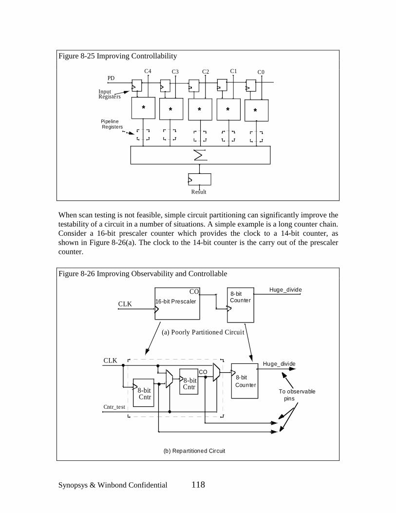
Synopsys & Winbond Confidential 118
When scan testing is not feasible, simple circuit partitioning can significantly improve thetestability of a circuit in a number of situations. A simple example is a long counter chain.Consider a 16-bit prescaler counter which provides the clock to a 14-bit counter, asshown in Figure 8-26(a). The clock to the 14-bit counter is the carry out of the prescalercounter.
Figure 8-25 Improving Controllability
Figure 8-26 Improving Observability and Controllable
* * * * *PipelineRegisters
C4 C3 C2 C1 C0
InputRegisters
PD
Result
(a) Poorly Partitioned Circuit
16-bit Prescaler8-bitCounter
Huge_divide
8-bitCounter
8-bitCntr
8-bitCntr
(b) Repartitioned Circuit
CLK
To observablepins
Cntr_test
CLK
CO
Huge_divideCO

Synopsys & Winbond Confidential 119
Note that this circuit violates a basic design rule which requires each clock to becontrollable. This violation will affect the implementation of a scan test method for thiscircuit. It is straightforward to test these counters without having to rely on the carry outsignal of the prescaler counter with the scan test method.
However, to fully test this circuit without the scan method, it would require 216*28, i.e.,over 16 M test vectors. It is possible to reduce the test vectors by using a pattern of"walking 1's" to exercise the overflow signal. Repartitioning the circuit to break theprescaler into two smaller blocks and multiplexing the clock directly to the second blockof the prescaler and to the 8-bit counter, as shown in Figure 8-26(b), will improve thecontrollability of the prescaler, as well as the counter. If the outputs of all three blocks canbe observed concurrently, the entire circuit can be tested in parallel with 28 test vectors.
A similar technique applies to circuits controlled by state machines. In the absence ofscan testing, the state machine can be bypassed to directly drive the output generationcircuitry in the test mode for direct testing.
You can use the following methods, in the order shown, to satisfy the controllability andobservability guidelines for a design:
� Inserting full scan� Inserting additional controllability and observability points
Figure 8-27 illustrtates improving the controllability and observability of a combinationalblock through the insertion of scan elements.
In Figure 8-27(a) the deep combinational block is partitioned into two blocks A and B; ascan flip-flop is inserted between them and included as part of an internal scan chain. Thevertical arrows through the scan flip-flops indicate a scan chain. During scan testing, thevalue of N can be captured into the scan flip-flop and shifted out for observation. Thescan element is used only for observability and does not have any functional use in the
Figure 8-27 Adding Controllability and Observability to a Circuit
(a) Observability only (b) Observability &
Inputs
Scan F/Ffor observ.
onlyTest_Mode
A B AN
B
Comb. Comb. Comb.
Comb.N
N’QD

Synopsys & Winbond Confidential 120
normal mode. The scheme illustrated in Figure 8-27(b) illustrates the improvement inboth observability and controllability of the internal pin through the addition of a scanflip-flop and a multiplexer. Note that the output of the scan flip-flop is connected to theinput of Block B, that is, pin N'. The scan flip-flop, as in (a), improves the observabilityof Block A. The mux makes it possible to control the input to Block B, by shifting thedesired value into N' into the scan flip-flop in the test mode. Although the mux does notalter the circuit functionality, it does add a delay to pin N in the normal mode. If the delaythrough the mux is unacceptable to your timing constraints, you can use simpler gates forthis purpose, as illustrated in Figure 8-28.
8.4.10 Analogy and Asynchronous Circuits
Lack of adequate observability and controllability make the task of testing analog orasynchronous circuits more difficult. If your ASIC contains asynchronous logic or analogcircuitry, provide direct access to these blocks from the primary inputs and outputs so thatthey can be tested directly from the device pins.
8.4.10.1 Black Box Cells
It is sometimes necessary to use cells that do not have their functionality characterized forthe test generation tool. Examples of such "black boxes" include:
� Embedded macros that do not have a structural equivalent� Logic that violates some testability rules
It is very important to isolate such cells from fault coverage considerations and providethe required controllability and observability for such cells.
You can detect problems with the controllability and observability of a circuit, early in thedesign cycle, by performing testability analysis with the RTL-code.
Figure 8-28 Adding Simple Gates to Improve Controllability
(b) Replacing N with ‘0’
A
B
Comb.
Comb.N’N
TestMode
(a) Replacing N with ‘1’
A
B
Comb.
Comb.N’N
TestMode1 in Test Mode 0 in Test Mode

Synopsys & Winbond Confidential 121
9. Language Constructs
9.1 Verilog Keywords
Verilog uses keywords, shown in the followings, to interpret an input file. You cannot usethese words as user variable names unless you use an escaped identifier.
always force or triregand forever output tableassign fork parameter taskbegin function pmos timebuf highz0 posedge tranbufif0 highz1 primitive tranif0bufif1 if pull0 tranif1case initial pull1 tricasex inout rcmos triandcasez input reg tri0cmos integer release tri1deassign join repeat vectoreddefault large rnmos waitdefparam medium rpmos wanddisable module rtran weak0end nand rtranif0 weak1endcase negedge rtranif1 whileendfunction nmos scalared wireendmodule nor small worendprimitive not strong0 xnorendtable notif0 strong1 xorendtask notif1 supply0event pulldown supply1for pullup trior
9.2 Unsupported Verilog Language Constructs
HDL Compiler does not support the following Verilog constructs:
� Unsupported definitions and declarations- primitive definition- time declaration- event declaration- triand, trior, tri1, tri0, and trireg net types- Ranges and arrays for integers

Synopsys & Winbond Confidential 122
- Unsupported statements- defparam statement- initial statement- repeat statement- delay control- event control- wait statement- fork statement- deassign statement- force statement- release statement- Assignment statement with a variable used as a bit-select onthe left side of the
equal sign� Unsupported operators
- Case equality and inequality operators (=== and !==)- Division and modulus operators for variables
� Unsupported gate-level constructs- nmos, pmos, cmos, rnmos, rpmos, rcmos, pullup, pulldown, tranif0, tranif1, rtran,
rtrainf0, and rtrainf1 gate
9.3 VHDL Reserved Words
The following lists the words that are reserved for the VHDL language and cannot beused as identifiers:
abs for packageaccess function portafter generate procedurealias generic processall guarded rangeand if recordarchitecture in registerarray inout remassert is reportattribute label returnbegin library selectblock linkage severitybody loop signalbuffer map subtypebus mod thencase nand tocomponent new transportconfiguration next type

Synopsys & Winbond Confidential 123
constant nor unitsdisconnect not untildownto null useelse of variableelsif on waitend open whenentity or whileexit others withfile out xor
9.4 VHDL Construct Support
Many VHDL language constructs, although useful for simulation and other stages in thedesign process, are not relevant to synthesis. Because these constructs cannot besynthesized, VHDL Compiler does not support them.
This section provides a list of all VHDL language constructs with the level of support foreach, followed by a list of VHDL reserved words.
A construct can be fully supported, ignored, or unsupported. Ignored and unsupportedconstructs are defined as follows:
� Ignored means that the construct is allowed in the VHDL source, but is ignored byVHDL Compiler.
� Unsupported means that the construct is not allowed in the VHDL source and thatVHDL Compiler flags it as an error. If errors arein a VHDL description, thedescription is not translated (synthesized).
Constructs are listed in the following order:
� Design units� Data types� Declarations� Specifications� Names� Operators� Operands and expressions� Sequential statements� Concurrent statements� Predefined language environment
9.4.1 Design Units

Synopsys & Winbond Confidential 124
entityThe entity statement part is ignored. Generics are supported, but only of typeINTEGER. Default values for ports are ignored.
architectureMultiple architectures are allowed. Global signal interaction between architectures isunsupported.
configurationConfiguration declarations and block configurations are supported, but only tospecify the top-level architecture for a top-level entity.
The use clauses, attribute specifications, component configurations, and nested blockconfigurations are unsupported.
packagePackages are fully supported.
libraryLibraries and separate compilation are supported.
subprogramDefault values for parameters are unsupported. Assigning to indexes and slices ofunconstrained out parameters is unsupported, unless the actual parameter is anidentifier.
Subprogram recursion is unsupported if the recursion is not bounded by a staticvalue.
Resolution functions are supported for wired-logic and three-state functions only.Subprograms can be declared only in packages and in the declaration part of anarchitecture.
9.4.2 Data Types
enumerationEnumeration is fully supported.
integerInfinite-precision arithmetic is unsupported.
Integer types are automatically converted to bit vectors whose width is as small aspossible to accommodate all possible values of the type range. The type range
can be either in unsigned binary for nonnegative ranges or in 2-complement form for

Synopsys & Winbond Confidential 125
ranges that include negative numbers.
physicalPhysical type declarations are ignored. The use of physical types is ignored in delayspecifications.
floatingFloating-point type declarations are ignored. The use of floating-point types isunsupported except for floating-point constants used with Synopsys-definedattributes.
arrayArray ranges and indexes other than integers are unsupported. Multidimensionalarrays are unsupported, but arrays of arrays are supported.
recordRecord data types are fully supported.
accessAccess type declarations are ignored, and the use of access typesis unsupported.
fileFile type declarations are ignored, and the use of file types is unsupported.
incomplete type declarationsIncomplete type declarations are unsupported.
9.4.3 Declarations
constantConstant declarations are supported except for deferred constant declarations.
signalRegister and bus declarations are unsupported. Resolution functions are supportedfor wired and three-state functions only. Declarations other than from a globallystatic type are unsupported. Initial values are unsupported.
variableDeclarations other than from a globally static type are unsupported. Initial values areunsupported.
fileFile declarations are unsupported.

Synopsys & Winbond Confidential 126
interfaceBuffer and linkage are translated to out and inout, respectively.
aliasAlias declarations are ignored.
componentComponent declarations that list a name other than a valid entity name areunsupported.
attributeAttribute declarations are fully supported; however, the use of user-defined attributesis unsupported.
9.4.4 Specifications
attributeOthers and all are unsupported in attribute specifications. User-defined attributes canbe specified, but the use of user-defined attributes is unsupported.
configurationConfiguration specifications are unsupported.
disconnectionDisconnection specifications are unsupported. Attribute declarations are fullysupported; however, the use of user-defined attributes is unsupported.
9.4.5 Names
simpleSimple names are fully supported.
selectedSelected (qualified) names outside of a use clause are unsupported. Overriding thescopes of identifiers is unsupported.
operator symbolOperator symbols are fully supported.
indexedIndexed names are fully supported with one exception. Indexing an unconstrainedout parameter in a procedure is unsupported.

Synopsys & Winbond Confidential 127
sliceSlice names are fully supported with one exception. Using a slice of anunconstrained out parameter in a procedure is unsupported unless the actualparameter is an identifier.
attributeOnly the following predefined attributes are supported: base, left, right, high, low,range, reverse_range, and length. The event and stable attributes are supported onlyas described with the wait and if statements. User-defined attribute names areunsupported. The use of attributes with selected names (name.name's attribute) isunsupported.
The following Synopsys-defined VHDL attributes are supported.
� Input port synthesis attributes
attribute ARRIVAL : real;attribute RISE_ARRIVAL : real;attribute FALL_ARRIVAL : real;attribute MAX_RISE_ARRIVAL : real;attribute MIN_RISE_ARRIVAL : real;attribute MAX_FALL_ARRIVAL : real;attribute MIN_FALL_ARRIVAL : real:
attribute DRIVE : real;attribute FALL_DRIVE : real;attribute RISE_DRIVE : real;
attribute EQUAL : boolean;attribute OPPOSITE : boolean;attribute LOGIC_ONE : boolean;attribute LOGIC_ZERO : boolean;
attribute DONT_TOUCH_NETWORK : boolean;
� Output port synthesis attributes
attribute LOAD : real;attribute UNCONNECTED : boolean;
� Component synthesis attributes
attribute DONT_TOUCH : boolean;

Synopsys & Winbond Confidential 128
� Design synthesis constraints
attribute MAX_AREA : real;attribute MAX_TRANSITION : real;
� Output port synthesis constraints
attribute MAX_DELAY : real;attribute MAX_FALL_DELAY : real;attribute MAX_RISE_DELAY : real;attribute MIN_DELAY : real;attribute MIN_FALL_DELAY : real;attribute MIN_RISE_DELAY : real;
9.4.6 Operators
logicalLogical operators are fully supported.
relationalRelational operators are fully supported.
additionConcatenation and arithmetic operators are fully supported.
signingSigning operators are fully supported.
multiplyingThe * (multiply) operator is fully supported. The / (division), mod, and remoperators are supported only when both operands are constant or when the rightoperand is a constant power of 2.
miscellaneousThe ** operator is supported only when both operands are constant or when the leftoperand is 2. The abs operator is fully supported.
operator overloadingOperator overloading is fully supported.
short-circuit operationThe short-circuit behavior of operators is not supported.
Synopsys & Winbond Confidential 129
9.4.7 Operands and Expressions
based literalBased literals are fully supported.
null literalNull slices, null ranges, and null arrays are unsupported.
physical literalPhysical literals are ignored.
stringStrings are fully supported.
aggregateThe use of types as aggregate choices is unsupported. Record aggregates areunsupported.
function callFunction calls are supported with one exception. Function conversions on inputports are not supported because type conversions on formal ports in a connectionspecification (port map) are not supported.
qualified expressionQualified expressions are fully supported.
type conversionType conversion is fully supported.
allocatorAllocators are unsupported.
static expressionStatic expressions are fully supported.
universal expressionFloating-point expressions are unsupported, except in a Synopsys-recognizedattribute definition. Infinite-precision expressions are not supported. Precision islimited to 32 bits; all intermediate results are converted to integer.
9.4.8 Sequential Statements
waitThe wait statement is unsupported unless it is of one the following forms:
Synopsys & Winbond Confidential 130
wait until clock = VALUE;wait until clock'event and clock = VALUE;wait until not clock'stable and clock = VALUE;
VALUE is '0', '1' or an enumeration literal whose encoding is 0 or 1. A waitstatement in this form is interpreted to mean "wait until the falling (VALUE is '0' orrising (VALUE is '1' edge of the signal named clock.?You cannot use waitstatements in subprograms or for loops.
assertionAssertion statements are ignored.
signalGuarded signal assignment is unsupported. The transport and after signals areignored. Multiple waveform elements in signal assignment statements areunsupported.
variableVariable statements are fully supported.
procedure callType conversion on formal parameters is unsupported. Assignment to single bits ofvectored ports is unsupported.
ifThe if statements are fully supported.
caseThe case statements are fully supported.
loopThe for loops are supported with two constraints: The loop index range must beglobally static, and the loop body must not contain a wait statement. The while loopsare supported, but the loop body must contain at least one wait statement. The loopstatements with no iteration scheme (infinite loops) are supported, but the loop bodymust contain at least one wait statement.
nextThe next statements are fully supported.
exitThe exit statements are fully supported.
returnThe return statements are fully supported.

Synopsys & Winbond Confidential 131
nullThe null statements are fully supported.
9.4.9 Concurrent Statements
blockGuards on block statements are unsupported. Ports and generics in block statementsare unsupported.
processSensitivity lists in process statements are ignored.
concurrent procedure callConcurrent procedure call statements are fully supported.
concurrent assertionConcurrent assertion statements are ignored.
concurrent signal assignmentThe guarded and transport keywords are ignored. Multiple waveforms areunsupported.
component instantiationType conversion on the formal port of a connection specification is unsupported.
generateThe generate statements are fully supported.
9.4.10 Predefined Language Environment
severity_level typeThe severity_level type is unsupported.
time typeThe time type is unsupported.
now functionThe now function is unsupported.
TEXTIO packageThe TEXTIO package is unsupported.

Synopsys & Winbond Confidential 132
predefined attributesThe predefined attributes are unsupported except for base, left, right, high, low,range, reverse_range, and length. The event and stable attributes are supported onlyin the if and wait statements.