william a. zortman - optoelectronics.ece.vt.edu
TRANSCRIPT

William A. Zortman
Candidate
ELECTRICAL AND COMPUTER ENGINEERING
Department
This dissertation is approved, and it is acceptable in quality and form for publication:
Approved by the Dissertation Committee:
Luke F. Lester , Co-Chairperson
Michael R. Watts , Co-Chairperson
Mani Hossein-Zadeh
Nasir Ghani
Anthony L. Lentine
ii
Design and Integration of Discrete Components for Low Energy WDM
Silicon Photonics on CMOS Systems
BY
William A. Zortman
B.S., Atmospheric Science, University of Arizona 1994
M.S., Electrical Engineering, University of New Mexico, 2008
iii
DISSERTATION
Submitted in Partial Fulfillment of the
Requirements for the Degree of
Doctor of Philosophy
Engineering
The University of New Mexico
Albuquerque, New Mexico
July, 2011

iv
DEDICATION
James, Rebecca and Samuel
v
ACKNOWLEDGMENTS
No effort of this magnitude gets done without a lot of help and inspiration.
My thesis committee fulfilled both of these. Professors Luke Lester, Mani Hossein-
Zadeh and Nasir Ghani are from the University of New Mexico. Professor (Adjunct,
UNM) Anthony L. Lentine is a Principal Member of Technical Staff at Sandia
National Labs. Professor Michael R. Watts is with the Massachusetts Institute of
Technology. Professors Lester and Watts were co-chairmen. I am very grateful for
their inspiration and the paths that they charted for those that follow them.
I would like to thank all of the people in Professor Lester’s Group at the
Center for High Technology Materials and Sandia’s Applied Photonics
Microsystems Department. In particular, Jeremy Wright was with me through this
whole process, and an unparalleled technical resource.
A PhD is an expensive proposition, but not for the student. This is because so
many institutions exist to fund research and support students. In my case these were
Sandia National Labs, the Defense Advanced Research Projects Agency,
Department of Energy, National Nuclear Security Administration, Sandia’s Lab
Directed Research and Development Program and the Veteran’s Administration.
Finally, and most importantly, I’d like to thank my wife Theresa for her
patience and for taking care of the things that grow at our house. Here’s a big
thumbs up to you girl!
vi
Design and Integration of Discrete Components for Low Energy WDM
Silicon Photonics on CMOS Systems
by
William A. Zortman
B.S. Atmospheric Science, The University of Arizona
M.S. Electrical Engineering, The University of New Mexico
Ph.D. Engineering, The University of New Mexico
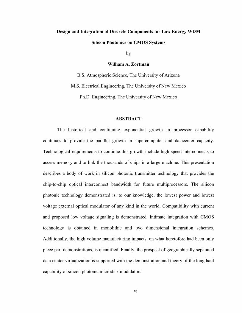
ABSTRACT
The historical and continuing exponential growth in processor capability
continues to provide the parallel growth in supercomputer and datacenter capacity.
Technological requirements to continue this growth include high speed interconnects to
access memory and to link the thousands of chips in a large machine. This presentation
describes a body of work in silicon photonic transmitter technology that provides the
chip-to-chip optical interconnect bandwidth for future multiprocessors. The silicon
photonic technology demonstrated is, to our knowledge, the lowest power and lowest
voltage external optical modulator of any kind in the world. Compatibility with current
and proposed low voltage signaling is demonstrated. Intimate integration with CMOS
technology is obtained in monolithic and two dimensional integration schemes.
Additionally, the high volume manufacturing impacts, on what heretofore had been only
piece part demonstrations, is quantified. Finally, the prospect of geographically separated
data center virtualization is supported with the demonstration and theory of the long haul
capability of silicon photonic microdisk modulators.

vii
Table of Contents Chapter One: Technologies for Off-‐Chip Communication .......................... 1
1. The Continuing Exponential Growth in Chip Capability ................................ 1
2. Outline of the Analysis in Chapter One ............................................................... 6
3. Processor Capability .................................................................................................. 8
4. Memory Architecture for Parallel Problems ................................................... 11
5. TSV ................................................................................................................................. 13
6. CMOS Embedded Memory Technology .............................................................. 17
7. Carbon Nanotubes .................................................................................................... 19
8. Signaling Technology .............................................................................................. 19
9. Summary of the Memory and On-‐Chip Signaling Outlook .......................... 21
10. The Trend of Computing Capability Quantified ........................................... 23
11. Chip-‐to-‐Chip Interconnect .................................................................................. 31
12. A Note on The Energy per Bit ............................................................................. 35
13. Summary and Overview of Subsequent Chapters ....................................... 37
14. References ................................................................................................................ 40
Chapter Two: Low Voltage Bias and Differential Signaling of a Low
Power High Speed Modulator ........................................................................................... 44
1. Introduction ............................................................................................................... 44
2. Analysis ........................................................................................................................ 45
3. Experimental Results .............................................................................................. 50
4. Conclusions on the Low Power Demonstration and a Note on BW ......... 57
5. Low Voltage Differentially Signaled Modulators ........................................... 57
6. Device Design and Electrical Connection ......................................................... 60

viii
7. Symmetric Drive ....................................................................................................... 61
8. Asymmetric Drive ..................................................................................................... 66
9. Energy per bit ............................................................................................................ 75
10. Summary ................................................................................................................... 76
11. References ................................................................................................................ 77
Chapter Three: Monolithic and Two-‐Dimensional Integration of
Silicon Photonic Microdisks with Microelectronics ................................................. 79
1. The Discrete Photonic Device .............................................................................. 81
2. Two-‐Dimensional Integration .............................................................................. 86
3. Monolithic Integration ............................................................................................ 92
4. Discussion ................................................................................................................... 98
5. References ............................................................................................................... 102
Chapter Four: Silicon Photonics Manufacturing ...................................... 104
1. Introduction ............................................................................................................ 104
2. Resonant frequency variation across wafers ............................................... 106
3. Demonstration of a new technique to extract dimensional variation 113
4. Within die variation ............................................................................................. 118
5. The Impact of non-‐uniformity ........................................................................... 127
6. Summary .................................................................................................................. 130
7. References ............................................................................................................... 132
Chapter Five: Long Haul Performance ........................................................ 134
1. Introduction ............................................................................................................ 134
2. Analysis ..................................................................................................................... 138
3. Experimental Results ........................................................................................... 147

ix
4. References ............................................................................................................... 154
Chapter Six: Conclusion .................................................................................... 155
1
Chapter One: Technologies for Off-Chip
Communication
1. The Continuing Exponential Growth in Chip Capability
Increasing the density of computing power on each die enables the growth of on-
chip computing capability. The density increase is necessary because the size of the die
cannot increase without introducing increased yield loss and therefore cost [1]. The clock
speeds of chips have been stuck at or below 5GHz since the early part of the millennium
because the amount of power that can be dissipated per cm2 on a die is limited. The limit
is about 100W/cm2 power dissipation on-chip [2]. Dissipated power is in direct
2
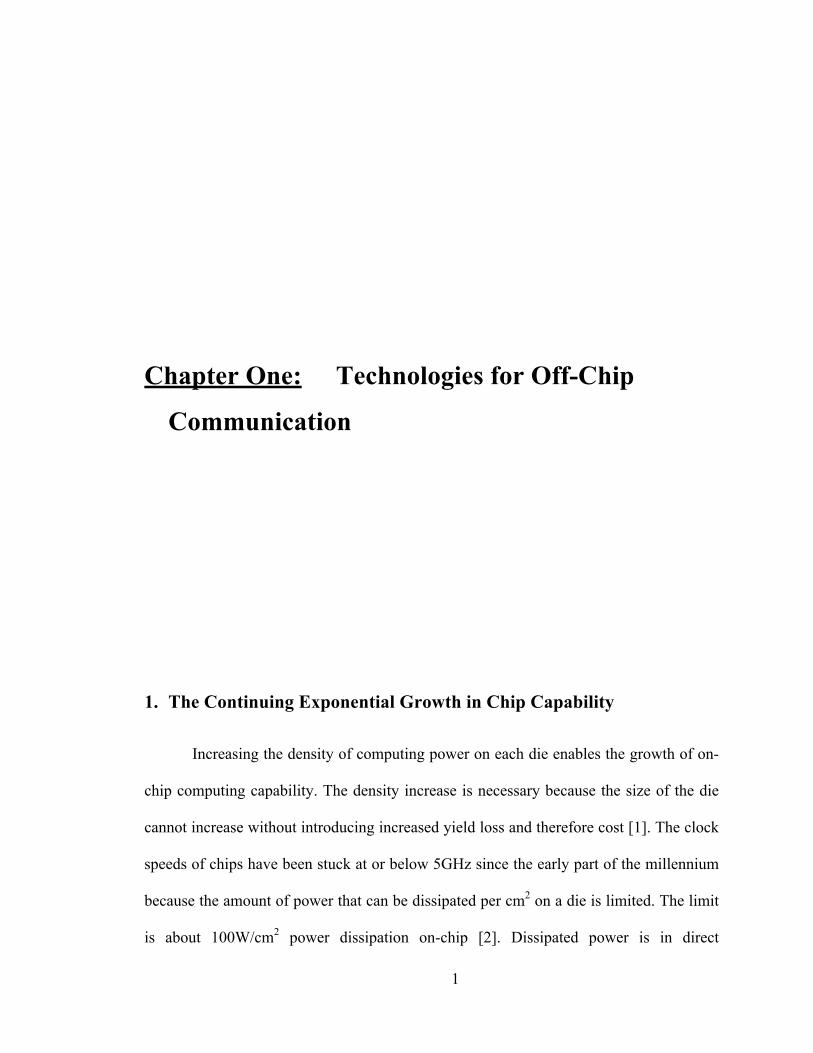
proportion to frequency; therefore simply increasing clock speed is not a clear method to
increase processing capability. And as Figure 1 shows the increase in clock speed is
stagnating. These limitations have meant that scaling transistor density is the primary
lever designers have to improve on-chip performance.
The requirements quickly lead to a long list of enabling technologies such as low-
k [3] and high-k [4] dielectrics and metal gates [5] on the materials side with low voltage
signaling [6], memory architecting [7] and multicore layout [8] on the electrical design
side [9]. Silicon processing capability is yet another area of innovation. Investigations of
future transistor technology will be left for others as the focus of this work is interconnect
and specifically what role optics will play. However, one important part of the transistor
solution is a call for cutting the supply voltage (Vdd) in half [10-13]. This is an important
factor that will be addressed in chapter 2 with new low voltage differential signaling
technology developed as part of this research.
This dissertation demonstrates the thesis that a silicon photonic resonant
modulator fabricated in crystalline silicon is a low power, high speed and manufacturable
solution for off-chip interconnect. It is also a practical one because its capacity for
wavelength division multiplexing allows a significant reduction in chip-to-chip fiber
interconnects. To fully appreciate this modulator’s advantages it is first necessary to
understand the role that it will fill in future interconnect schemes. This is done in the
introductory chapter.
3
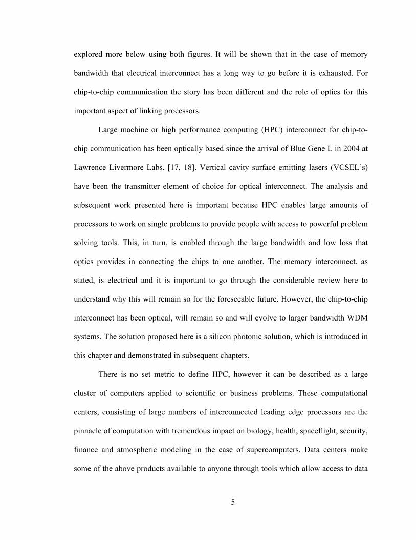
Figure 1 The growth and leveling out of clock frequency in microprocessors [10].
4
The focus of this chapter is to evaluate the chip communication bandwidth and
assess in a holistic manner the converging capabilities of multicore layout, memory
architecting, off-chip low voltage signaling, new materials and optics against the growing
need for memory and off-chip bandwidth in an environment with decreasing energy
available for each bit transmitted. The implementation and type of optics on-chip or close
to the chip will be evaluated based on these factors. The approach is to assess chips
designed for server applications because designers of these products will have to
overcome all of the above issues in an environment that then requires the chips to be
interconnected. Additionally, these chips are used in critical infrastructure of the modern
economy, research and security agencies. Analysis of this topic for application specific
integrated circuits (ASIC’s) can be found in [14]. Additionally, the chips considered are
used in servers for supercomputing and high performance data centers.
As already stated, the major focus is bandwidth. As on-chip performance
(transistor density and on-chip interconnect) continues to improve designers must also
provide the requisite increased access to memory. In 2003 the National Science
Foundation published a blue-ribbon report outlining memory bandwidth requirements,
which consisted of greater than 1 byte/flop for processor-memory interaction [15]. The
figures presented are for a balanced large-scale system such as a supercomputer. It is
noted that off-chip memory bandwidth of 1 byte/flop is often quoted as a requirement for
computation [14]. Another standard of only 0.5Byte/FLOP may also be used because it is
expressed in a more recent study on supercomputing [10] and is also the capability of the
latest and world’s most powerful supercomputer being installed at the University of
Illinois by IBM called Blue Waters [16]. The subject of memory bandwidth will be
5
explored more below using both figures. It will be shown that in the case of memory
bandwidth that electrical interconnect has a long way to go before it is exhausted. For
chip-to-chip communication the story has been different and the role of optics for this
important aspect of linking processors.
Large machine or high performance computing (HPC) interconnect for chip-to-
chip communication has been optically based since the arrival of Blue Gene L in 2004 at
Lawrence Livermore Labs. [17, 18]. Vertical cavity surface emitting lasers (VCSEL’s)
have been the transmitter element of choice for optical interconnect. The analysis and
subsequent work presented here is important because HPC enables large amounts of
processors to work on single problems to provide people with access to powerful problem
solving tools. This, in turn, is enabled through the large bandwidth and low loss that
optics provides in connecting the chips to one another. The memory interconnect, as
stated, is electrical and it is important to go through the considerable review here to
understand why this will remain so for the foreseeable future. However, the chip-to-chip
interconnect has been optical, will remain so and will evolve to larger bandwidth WDM
systems. The solution proposed here is a silicon photonic solution, which is introduced in
this chapter and demonstrated in subsequent chapters.
There is no set metric to define HPC, however it can be described as a large
cluster of computers applied to scientific or business problems. These computational
centers, consisting of large numbers of interconnected leading edge processors are the
pinnacle of computation with tremendous impact on biology, health, spaceflight, security,
finance and atmospheric modeling in the case of supercomputers. Data centers make
some of the above products available to anyone through tools which allow access to data
6
center computing applications like Wolfram Alpha [19]. Additionally, data centers are
providing catalyst to improved quality of life and considerable economic and political
shifts through a variety of social networking tools.
2. Outline of the Analysis in Chapter One
With this in mind the focus of this introductory chapter is to appropriately target
the right optical solutions for enabling HPC interconnect. The focus of the analysis is on
the individual chip in order to create a set of requirement for interconnects. The reader
will also be left with insight into the performance of the discrete part. There are three
questions to ask in order to do this. The first is whether or not the on-chip interconnects
between registers and caches can handle the bandwidth and energy requirements with
electrical signaling. This is among the easiest to answer because it is addressed directly
by the International Technology Roadmap for Semiconductors (ITRS). The answer to this
is yes not just because electronics is capable, but also because optical integration on-chip
is more difficult than integration of new lower-k dielectrics that reduce the capacitance in
on-chip electrical lines [20]. The second question is whether or not electronics can handle
the local memory bandwidth, that is the communication to local memory to supply the
processing cores with enough data to take advantage of their processing capability. The
answer here is also yes largely because so many solutions exist or are on the ITRS
roadmap to keep this within the realm of electronics. The technologies will be reviewed
in a considerable part of the text. A reader already familiar with CMOS technology and
the emerging electrical interconnect and memory hierarchy technologies may want to
skip to the section titled “The trend of computing capability quantified.” The third
7
question is whether or not chip-to-chip interconnect can be handled electronically. The
answer is no. Already, optical interconnect using VCSEL’s handle communication
between the cabinets which house the servers and chips in large machines and they are
moving closer to the chip each year to provide blade to blade, board to board and
eventually chip-to-chip communication. The more important result here is that the current
single channel per fiber VCSEL technology will begin to lose practicality and another,
wavelength division multiplexed (WDM) technology, will be required. The proposed
technology is WDM silicon photonics, which is also the subject of the subsequent
chapters.
A key outcome, which is also addressed below, is that the optics can remain off of
the processor, greatly simplifying fabrication and enabling very low power crystalline-
silicon photonic interconnects. The other key outcome is that although optics will remain
off-processor, it must get closer to the processor, take advantage of advanced off chip
electrical interconnect and evolve into a WDM system.
To address the above open questions a review of processor capability is first given
followed by a discussion of parallel problems, which best illuminate the strengths of
memory hierarchy, an important piece of the interconnect problem. Then a review of off-
chip interconnect technology is given including through silicon vias (TSV) which is seen
to be a key technology for enabling additional high speed off-chip optical interconnect.
Current and future capabilities for electrical signaling are reviewed because we would
like to know when signaling through the currently used techniques such as the ball grid
array will be saturated, requiring the use of TSV’s. Finally, trends in chip capability and

8
interconnect requirements will be analyzed to reveal the lifetime of the emerging
interconnect technologies.
3. Processor Capability
One important goal of new server chip designs is to increase the number of
floating point operations per second (FLOPS) within the power and bandwidth
constraints mentioned in the first section. A FLOP is an operation on two floating-point
(decimal) inputs. With clock rates static, processors designed with multiple cores
allowing parallel execution of instructions have allowed the continuous exponential
increase in processing power. This has not been a perfect answer because the advantage
of this strategy applied to existing software levels off with increasing cores in compliance
with Amdahl’s law [21]. However, an important corollary to Amdahl is that multicore
processing will enable chips to handle more complex software, and therefore larger, more
complex problems, seemingly without limit [22]. The additional cores have enabled an
increase in FLOPS. Assuming on-chip interconnect can handle the increased transistor
density, multicore processing is advantageous especially for a server chip with
application in a supercomputer designed to deal with larger and more difficult problems
in every generation.
On-chip interconnect can also include the interconnect capability to memory.
Often this is referred to as off-chip memory bandwidth, but contemporary microprocessor
memory architecture locates significant memory on-chip in static random access memory
(SRAM) cache. An example of this is the IBM Power 7 processor being used in the Blue
Waters machine, which has 32MB of memory on each processor in static random access

9
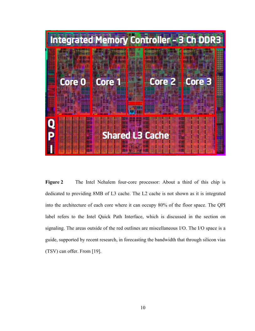
memory (SRAM). Another example is the Intel Nehalem (part of the Itanium family)
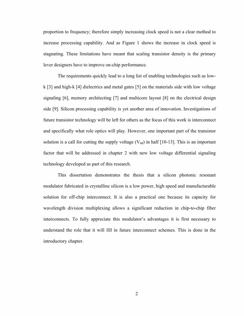
processor shown in Figure 2, which also shows that cache occupies more than half of the
modern processor floor space. This type of memory can be used as a shared scratchpad so
that a core could process a FLOP, write it to cache and then another core or the same core
could use that result. This saves the bandwidth of writing and reading from an off-chip
memory source. Advances in chip packaging utilizing through silicon vias (TSV), for
example, will make access to some random access memory (RAM) so close that the vias
connecting it to the memory chip will not be significantly longer than interconnects on-
chip. Memory bandwidth therefore refers to very short links on-chip to cache or to a local
dynamic RAM (DRAM) chip. It is appropriate to consider this bandwidth as separate
from chip-to-chip bandwidth, which covers larger distance between processors.
To summarize, processor density has increased the number of FLOPS and this is
only possible with the support of timely access to memory. So interconnect to memory
and assessment of its current and future ability really is a discussion of on-chip and short
off-chip links in addition to methods for incorporating new types of memory on-chip,
which will be explored next.
10
Figure 2 The Intel Nehalem four-core processor: About a third of this chip is
dedicated to providing 8MB of L3 cache. The L2 cache is not shown as it is integrated
into the architecture of each core where it can occupy 80% of the floor space. The QPI
label refers to the Intel Quick Path Interface, which is discussed in the section on
signaling. The areas outside of the red outlines are miscellaneous I/O. The I/O space is a
guide, supported by recent research, in forecasting the bandwidth that through silicon vias
(TSV) can offer. From [19].

11
4. Memory Architecture for Parallel Problems
Microprocessor technology employs on-chip SRAM cache for data that needs to
be quickly accessed. The idea that some RAM is more time sensitive than other RAM
implies a hierarchical model, which seeks to balance latency with bandwidth. Reducing
the memory access time is driven by interconnect technology and memory hierarchy.
Having memory close to the cores limits latency.
There are generally three levels of cache L1, L2 and L3 although different designs
parse chip area differently between the three types of cache and some exclude L3. L1
cache is usually located at the processor core and typically can be a register. L2 cache is
almost exclusively SRAM and can serve as a backup to L1 or serve as a scratchpad as
mentioned above for the different cores or threads within a core. So if a process does not
find the needed data or instruction in L1 (an event called cache miss) it can search in L2.
L3 cache is a further backup, but not designated to a particular thread or processor so it
serves as a chip wide memory backup or as a way to transfer the output of one core to the
input of the next saving a longer latency call to DRAM. Memory migration toward
processor cores has been an ongoing trend. One can even think of DRAM in the
architecture as a type of “L4” cache since its primary purpose is to avoid the long latency
associated with access to hard disk memory.
Memory hierarchy is an area that has gained a lot of attention in its application to
multiprocessor chips used to solve large problems i.e. on supercomputers. For example,
Intel’s terascale chip project [23] aims to incorporate 80 or more cores on a single chip
[24]. Large parallel problems typically include binomial trees for financial simulation,
Monte Carlo analysis, finite difference time domain (FDTD) and fast Fourier transform
12
(FFT) for photo and video rendering [25]. These are parallel applications utilizing Single
Instruction Multiple Data (SIMD) instruction, that is they do the same calculation on
meshed data requiring limited calls to shared memory (DRAM) [26]. The multithreaded
nature of the software used for these problems rely almost strictly on cache. Therefore, it
is possible to segment shared memory (L3 cache) to one part of the chip and allow more
room for L1 and L2 level cache local to each core. Even as RAM has moved on-chip,
application specific cache architecture is allowing high performance chips to avoid long
latency access to a DRAM chip while still providing enough memory bandwidth to solve
these less memory intensive problems.
Yet even as memory hierarchy advancements achieve greater memory bandwidth
and allow designers the granularity to move memory from DRAM to SRAM, SRAM still
does not have DRAM’s density. This means that SRAM is not as efficient area wise if we
were able to say, move the DRAM onto the chip. Potentially a memory cell could be
devised which is interchangeable with logic. The idea to have memory cells that are
interchangeable with logic will be addressed briefly below.
Memory hierarchy and especially large cache on-chip have enabled rapidly
advancing microprocessors to maintain enough memory bandwidth to take advantage of
the advances. This is especially true for problems that are largely parallel. For more
general problems strategies in addition to smart hierarchy and caching can be employed
[23]. This is explored next.
13
5. TSV
Through silicon via or TSV is a viable technology because it is an extension of
existing via technology already used in the industry. A TSV is a vertical connection
between two chips, which enables vertical stacking of chips [27].
If the TSV is not significantly longer than the existing vias on a microprocessor
then electrically the TSV connected cells can provide very quick access to memory.
Technologies that vertically stack chips will have the largest impact and some see it as a
potential technology to enable the replacement of SRAM [28]. TSV’s require adequate
alignment between the chips being connected. Tight tolerance and repeatable alignment
to within a 3µ has already been demonstrated [29]. In the case of [29] alignment was tight
enough to enable an optical via. TSV via lengths are typically on the order of 10µm; they
are about the height of a nine metal layer vertical stack [30].
Recent investigations into TSV’s show that high data rate and low latency is
possible with the limitations of heat dissipation and threshold voltage shift on-chip. The
Interuniversity Microelectronics Center (IMEC) in Belgium recently assessed TSV
capabilities [30]. The test involved fabricating 41 stage ring oscillators monolithically on
a chip and then comparing them to ring oscillators that bounded between chips using
TSV’s (a common multichip packaging test strategy). In the experiment no degradation
in speed or power was seen when two TSV’s were used to connect the chips. Another
demonstration by Kawano et al showed a 3Gbps data rate using TSV’s in 2008.
Some of the issues with TSV’s include threshold voltage shift for transistors near
the TSV and heat retention from chip stacking. The value for threshold voltage shift is in
the range of 10mV [31] near TSV’s and there can be up to 3X the heat retention[32].
14
Possibly stacking memory on parts of the chip, which run at a lower clock cycle and are
cooler, would alleviate this problem [28]. While TSV’s are electrically capable of
providing interconnect to memory or an optical chip there are the challenges of heat
dissipation and shifting transistor thresholds that must be considered. These two aspects
contribute to the fact that TSV’s are not capable of covering the entire chip, which is an
important factor in evaluating the bandwidth TSV’s can provide.
In addition to the individual demonstrations above, work has also been done in
light of the limitations given to assess the total bandwidth that TSV’s may provide. TSV
capabilities have been theoretically examined [33], simulated [34] and fabricated [35].
One can imagine vertical interconnects packed densely onto a chip limited in bandwidth
by the RC time constant of the individual and coupled lines. As the lines become thinner
and packed more tightly the number of channels increase yet the resistance and wire-to-
wire capacitance and inductance also increase. Theoretical studies of TSV’s support
analysis of TSV’s as lumped electrical lines and that standard estimation of resistance
and capacitance can be used [33, 35], agreeing well with simulation [36].
Theoretically TSV’s can achieve 10Ebps/mm2 [33] which translates into a
Ybps/cm2. This assumes that the entire area can be used for TSV’s and the electrical
driver runs at 100PHz. This is not the case. Microprocessors can use fully 2/3 of solder
bumps for power and ground and these connections will always be present. Additionally,
not all of the chip can be used for TSV’s because they interfere either with on-chip
interconnect or take up valuable transistor space. In [35] it is assumed that only 1-5% of
the microprocessor can be used for TSV’s.
15
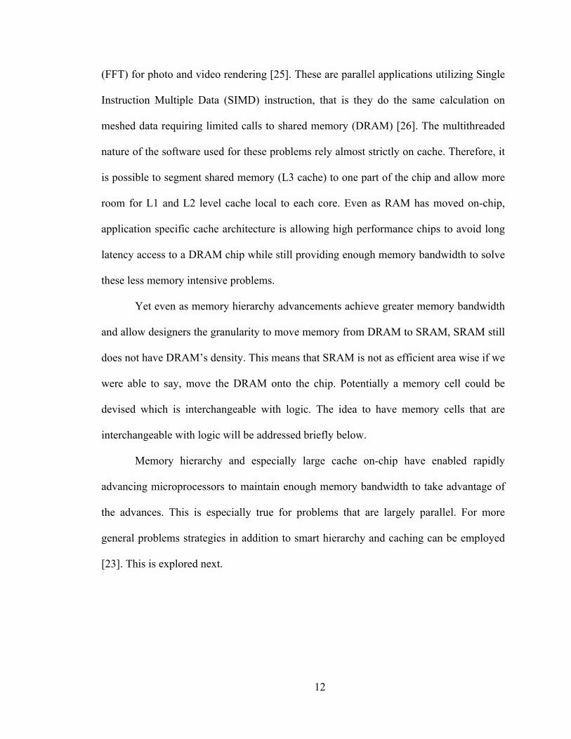
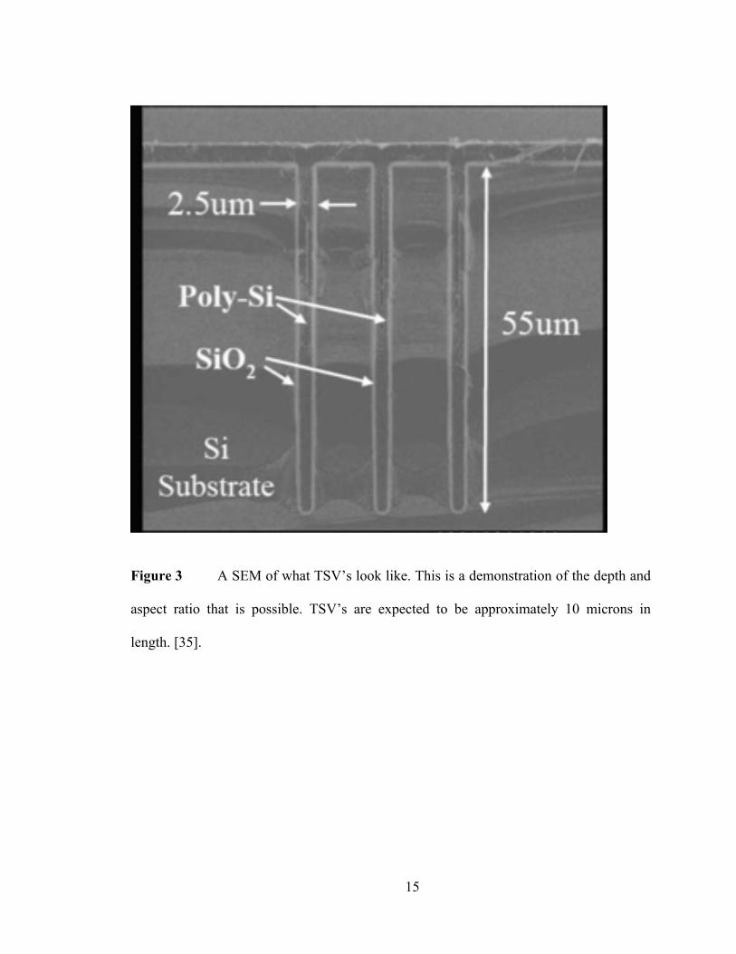
Figure 3 A SEM of what TSV’s look like. This is a demonstration of the depth and
aspect ratio that is possible. TSV’s are expected to be approximately 10 microns in
length. [35].

16
Figure 4 Conceptual drawing of TSV technology. TSV’s are likely limited to the
normal I/O regions of the chip as shown in Figure 1 and expanding this area risks
impacting the threshold voltages of the processors [35]. This particular stack does not
contain an optical chip, but one could be added anywhere in the stack provided the fibers
are side coupled. (Micron Inc.)
17
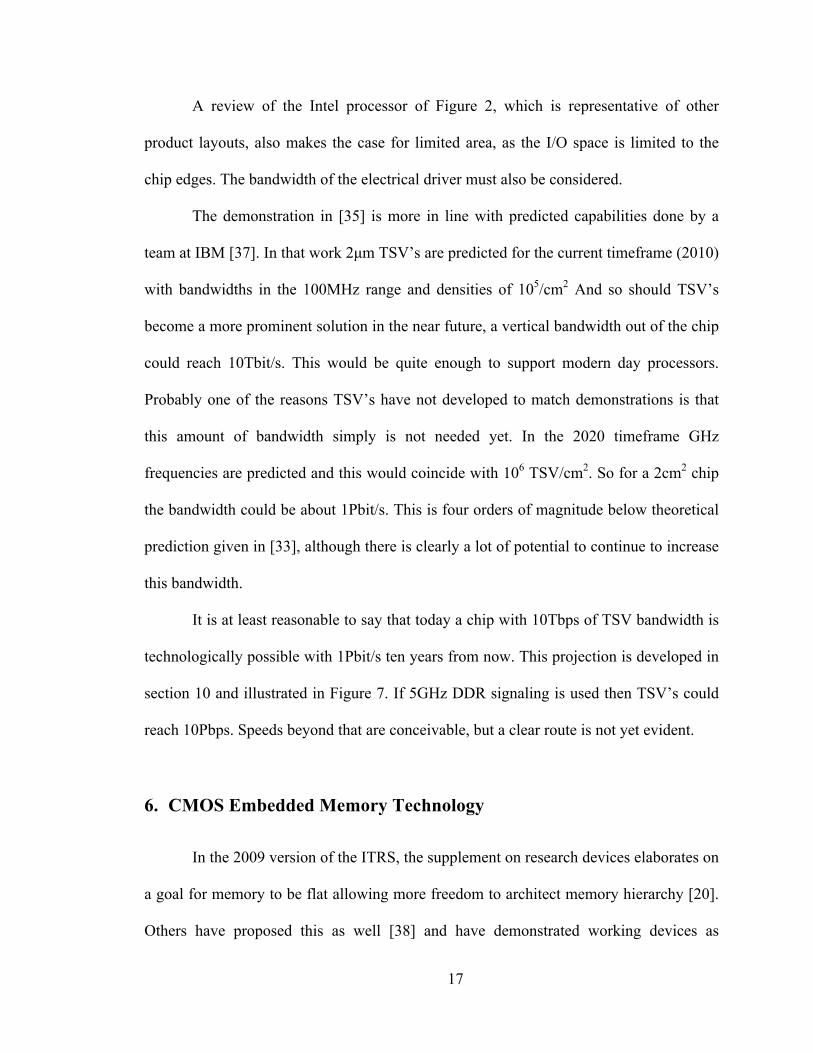
A review of the Intel processor of Figure 2, which is representative of other
product layouts, also makes the case for limited area, as the I/O space is limited to the
chip edges. The bandwidth of the electrical driver must also be considered.
The demonstration in [35] is more in line with predicted capabilities done by a
team at IBM [37]. In that work 2µm TSV’s are predicted for the current timeframe (2010)
with bandwidths in the 100MHz range and densities of 105/cm2 And so should TSV’s
become a more prominent solution in the near future, a vertical bandwidth out of the chip
could reach 10Tbit/s. This would be quite enough to support modern day processors.
Probably one of the reasons TSV’s have not developed to match demonstrations is that
this amount of bandwidth simply is not needed yet. In the 2020 timeframe GHz
frequencies are predicted and this would coincide with 106 TSV/cm2. So for a 2cm2 chip
the bandwidth could be about 1Pbit/s. This is four orders of magnitude below theoretical
prediction given in [33], although there is clearly a lot of potential to continue to increase
this bandwidth.
It is at least reasonable to say that today a chip with 10Tbps of TSV bandwidth is
technologically possible with 1Pbit/s ten years from now. This projection is developed in
section 10 and illustrated in Figure 7. If 5GHz DDR signaling is used then TSV’s could
reach 10Pbps. Speeds beyond that are conceivable, but a clear route is not yet evident.
6. CMOS Embedded Memory Technology
In the 2009 version of the ITRS, the supplement on research devices elaborates on
a goal for memory to be flat allowing more freedom to architect memory hierarchy [20].
Others have proposed this as well [38] and have demonstrated working devices as
18
prototypes for future teraflop chips [39, 40]. Although it should be clear that embedded
DRAM could come in two flavors: as a block of dedicated memory or as a new logic cell
that can be programmed as memory or logic. As discussed above, memory architecture
designers create an architecture that allows fast access to quickly needed data and slower
access to other data, which can be queued or is less time critical. The hierarchy levels are
in general cache memory, random access memory and storage. With new processing it
may be possible to build a technology that the ITRS describes as having the “speed and
re-writability of SRAM, density of DRAM and persistence of flash”. Although
persistence may be unnecessary, certainly an array of logic built on memory cells or
partly built on memory cells would be fast and scalable. This idea of programmable logic
is akin to the architecture of field programmable gate arrays (FPGA’s) which are
reprogrammable blocks of SRAM memory which can pull double duty as “block
DRAM” if desired. For operations requiring rapid access to memory, the programmable
logic would allocate more resources to provide embedded memory, what designers today
would call cache. If it is assumed that memory chips would be made of this same
optimized type of cell, scaling the chip would essentially turn into a virtualization
exercise in a 3D package where logic could reside on multiple levels with the memory
which it needs access to. Although this would seem to solve the off-chip memory
bandwidth problem, it does not link chips or blocks of virtualized chips to each other. A
large bandwidth will still be required to handle the large number of FLOPS in this
architecture and a stacking technology is still needed.
The implications for this technology reach beyond a solution to interconnect
issues. Flat memory-logic architecture enables highly dense programmable logic where
19
the only differentiation manufacturers will be able to claim is price, quality and
programming tools. Design would be done in the field potentially generating many
custom solutions to computing problems.
7. Carbon Nanotubes
Carbon nanotubes (CNT) are another possibility for improving both on-chip and
off-chip interconnect and discussion about interconnect would be incomplete without
mentioning them. Additionally, because they introduce a new material into the
manufacturing process of CMOS, one has to ask why they wouldn’t be considered with
optical technology, which also requires new material introduction to the backend
processing. CNT’s are attractive because they allow the use of electronic signaling so
there is no need to integrate optics or convert quanta. Additionally, their electronic
properties allow them to be used as interconnect all the way down to the transistor level
(with impedance matching), a place where optics would not easily integrate. Initial work
evaluating CNT’s for interconnects predicts a 30% improvement in both energy and
resistance performance and this should only improve as more research is conducted [41].
A recent review of the work done in Grenoble, France by CEA LITEN suggests CNT
technology for vias could be ready in 2015 and claims up to a 1000 fold increase in
current carrying capability over copper [42].
8. Signaling Technology
New processing and layout for microprocessors have been described above. The
other piece is the signaling that will carry the information to and from the memory. Here
20
a contemporary microprocessor signaling technology will be reviewed to provide insight
into the bandwidth available to chips in their current configuration. The signaling is used
in a board layout and the technology described here is similar to other manufacturers’
solutions. Finally, a brief review of leading edge research into low voltage signaling is
provided so that a prediction about when off-chip links though solder bumps will be
exhausted requiring some sort of chip stack or other technology to intervene.
The current needs of off-chip memory bandwidth are handled using low voltage
signaling (LVS) (LVS here is used generally to encompass a wide range of differential
signaling technologies which operate at low voltage). One example of this is Intel’s
QuickPath Interface (QPI) architecture (AMD has a similar solution called
HyperTransport), which improves on the uni-directional front side bus designs used
previously. QPI is a point-to-point link that uses differential signaling [43]. The QPI is
used on the current Itanium and Xeon server processors [44] and although it is not for
memory interconnect, it is a state of the art design that can be used to gauge the capacity
of contemporary electrical CMOS signaling. The QPI interface can run at 204.8Gbps
using 84 pins so it has about 2.5Gbps per pin bandwidth. The 2011 Xeon Westmere chip,
which is a ten-core processor has 1560 pins. If 2/3 of the pins are power and ground then
at most the chip could have 1.3Tbps off-chip bandwidth for memory and connection to
other chips as well.
Comparing this to research, Kim et al. have recently demonstrated a 356 fJ/bit 1
cm CMOS link using an equalized transmitter in low voltage differential signaling
(LVDS) at a 4Gbps rate [45]. This is on a single line. A claim is made in this paper for
5.2Gbps using 462.8fJ/bit. (In a theoretical prediction for LVS in 1997 Dally concluded a
21
4Gbps link would be possible [46].) If it is assumed that this type of signaling can be
integrated into an advanced CMOS process (it was originally done in 90nm technology)
then we might expect 2X the speed of the QuickPath link in a future generation.
Additional scaling of the ball grid array may get additional bandwidth and so, again, the
bandwidth could realistically be doubled to 2.6Tbps off-chip bandwidth. At 1 byte/FLOP,
and considering memory alone, this bandwidth is sufficient for a 325GFLOP processor
and at 0.5byte/FLOP the ball grid array (BGA) can support 650GFLOPs, which will be
within the capability of server chips at about 2014 (Figure 5).
In the preceding discussion concern was not given to the type of interconnect used
for different jobs. For example, memory is accessed on todays processors using a slower
memory controller that runs in the hundreds of MHz. The analysis is done using the
fastest and densest interconnect used today with the assumption that designers will
exhaust those tools before moving to completely new interconnect technology.
9. Summary of the Memory and On-Chip Signaling Outlook
Processor capability continues to increase at an exponential pace and the next
section will confirm this is the case. It may be tempting to look at on-processor optics
with its lack of RC limitations, high frequency carrier wave and multiplexing capability
as a solution for intra-chip and off-chip memory interconnect. However, for these
categories of interconnect many solutions exist.
The ITRS has identified ways to maintain the on-chip interconnect RC bandwidth.
This ITRS already dedicates an entire supplemental report on interconnect in each edition
of its roadmap and the solutions are a continuum of the quest for lower-k dielectrics. This
22
type of interconnect faces growing challenges to implement, although according to the
International Technology Roadmap for Semiconductors Interconnect supplement
mentioned above, copper integrated with low-k dielectrics will provide enough
bandwidth at least until 2020 [20]. Air gaps are forecast to take over after that time and
air gap interconnect has been demonstrated already at IBM [47]. CNT was briefly
mentioned as another possible solution on this front. Backend optical materials like poly-
silicon and nitride waveguides require either too high of a temperature (in the case of
poly) [48] or are not active semiconductors in the case of nitride meaning yet another
material is needed to modulate the optics [49]. These problems are surmountable, but
simply may not be needed. It is hard to imagine that these problems are much easier to
overcome than implementing lower-k oxides although it seems as if ease of integration is
a more pertinent question than whether or not the electrical bandwidth will be available.
In the case of memory bandwidth the evolving cache architecture has meant that
going off-chip is not necessary for all of the memory. Further research is exploring ways
to implement ubiquitous gate technology that would allow chips to be programmed for
the amount of local and off-chip embedded memory needed to optimize performance.
However, even in that case, off-chip connection is required and when going off-chip TSV
appears to be a technology that is able to support off-chip memory interconnect in a 3D
stack. While TSV technology is not seen in today’s leading edge chips, electrical
signaling technology through the BGA is adequate at least until the middle of the decade.
The conclusion is therefore that electronics is the favored solution for on-chip
interconnects and off-chip memory interconnects. The remaining interconnects to
consider is the chip-to-chip interconnect which is done in the remainder of the
23
introduction. Quantification of processor capability is needed for this discussion and so
the processor will be revisited in more detail next.
10. The Trend of Computing Capability Quantified
In order to understand the off-chip memory bandwidth required in the future, use
will be made of the memory bandwidth set forth by the NSF and the recent HPC study
done for DARPA which were outlined earlier. Recall the NSF figure is 1Byte/FLOP and
the DARPA report called for 0.5Byte/FLOP. Additionally, the performance increase in
FLOPS over the last several years will be used to project future performance. With these
two numbers the required off-chip bandwidth for both memory and chip-to-chip I/O can
be calculated.
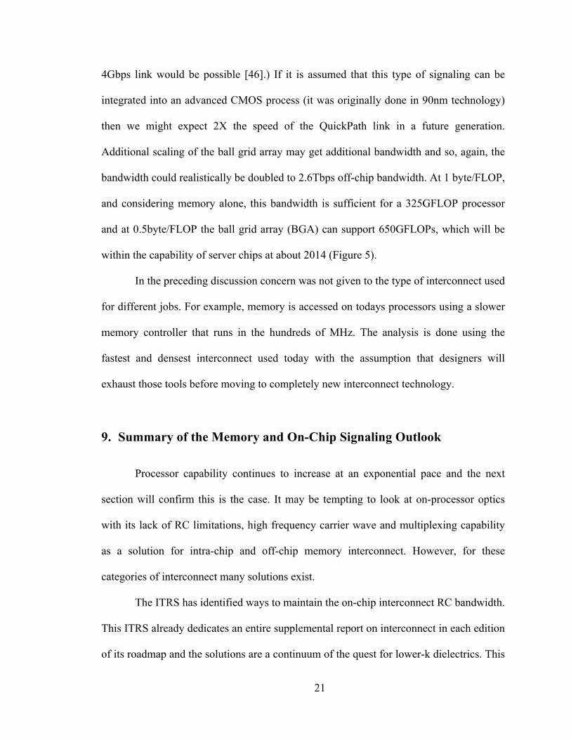
Several plots of data are to be used. The first plot in Fig 5 gives the theoretical
performance and measured performance of individual processors. The theoretical
performance here is estimated from the following formula which is consistent with [50]:
GFLOPS = Ncores !operations
core! fclock (GHz)
(1)
In the above equation Ncores is the number of cores in the microprocessor. The
operationss/core refers to the number of operations a core can run in a single cycle. It is a
loaded figure, its details are not necessary for this analysis, however they wil be briefly
described. The operations/core is a function of the number of threads that each core can
run and the number of instructions it can fetch. Both of these are in turn a function of the
operating system and application, which is why the outcome is a theoretical peak. A
thread is a part of a larger process running in a single core, within a single clock cycle,

24
but not necessarily at the same time. Instructions are the decoded input that arrives on the
core registers. Modern cores read more than one per clock cycle. fclock is the clock
frequency. In this work it will be written in units of gigahertz so the number of FLOPS
will be stated in GFLOPS.

25
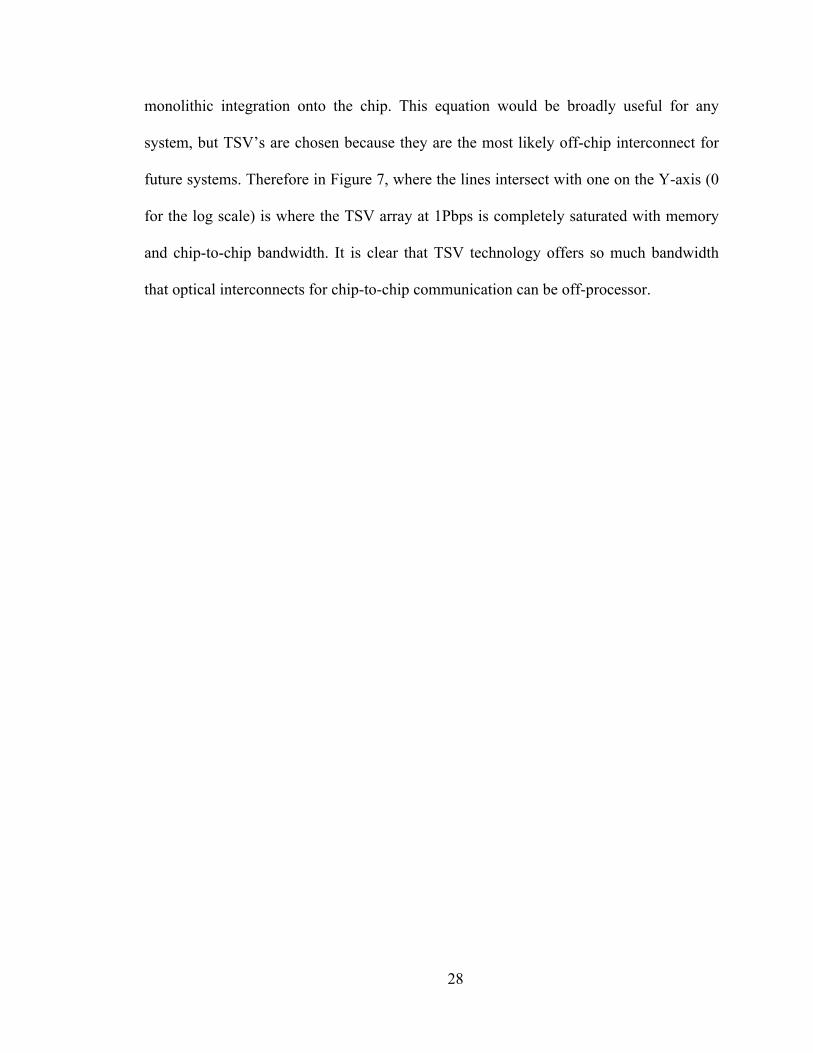
Figure 5 The theoretical and measured performance of modern server chips. The
values for theory are found by using equation 1 and also explained in the text following
that equation. The discrete chip values are independent measurements using LINPACK
for individual chip performance. The measured data TOP SC is found by dividing the
number of chips in recent top supercomputer designs into the number of FLOPS the HPC
system operates at giving an average number of FLOPS the chips operate at when
integrated into HPC applications. This value is used to generate the fit line to forecast
future chip performance and it is used for the lower bound of FLOP performance that
memory and off chip bandwidth must support.
2000 2010 20202
0
2
4
6
Year
Log
GFL
OPS
Chip FLOPs
TheoryDiscreteTOP SCFitTFLOP

26
For example, a version of the AMD Magny-Cours processor released in 2010 has
10 cores, can execute 12 operations per cycle, and runs at 2.3GHz. Therefore its
theoretical performance is 276 GFLOPS. However, the chip only runs this fast with
massive parallelism (SIMD). In most benchmark tests this is not the case.
In 2008 a team at Lawrence Berkeley Labs (LBL) tested processors for their
performance under different conditions [50]. Two of the processors were Intel’s
Clovertown and AMD’s Barcelona. The test was done using two each of these quad core
processors in a dual socket configuration for a total of eight cores each with a theoretical
peak performance of 74.64 GFLOPS for the Intel system and 73.6 GFLOPS for the AMD
system. The study found that when the data is parallelized (SIMD) the chips can get to
about half of their peak performance. When the data is not parallelized only about a
quarter of the peak performance is realized.
Additionally, testing of processors is quite an active area for which
microprocessor enthusiasts like to report their results on discrete parts. In most cases the
tests using the linear algebra computing standard called LINPACK result in about 25% of
the theoretical limit. One can also take the FLOPS of the top supercomputers over the last
two decades and divide these values by the number of processors incorporated in the
machine. The results in this case yield about a third of the peak performance for these
chips integrated into HPC environments. This data is summarized in Figure 5. Based on
this data, calculations can be done to assess the required memory and off-chip bandwidth
required and more importantly to determine if emerging off-chip signaling technology
can handle these data rates.
27
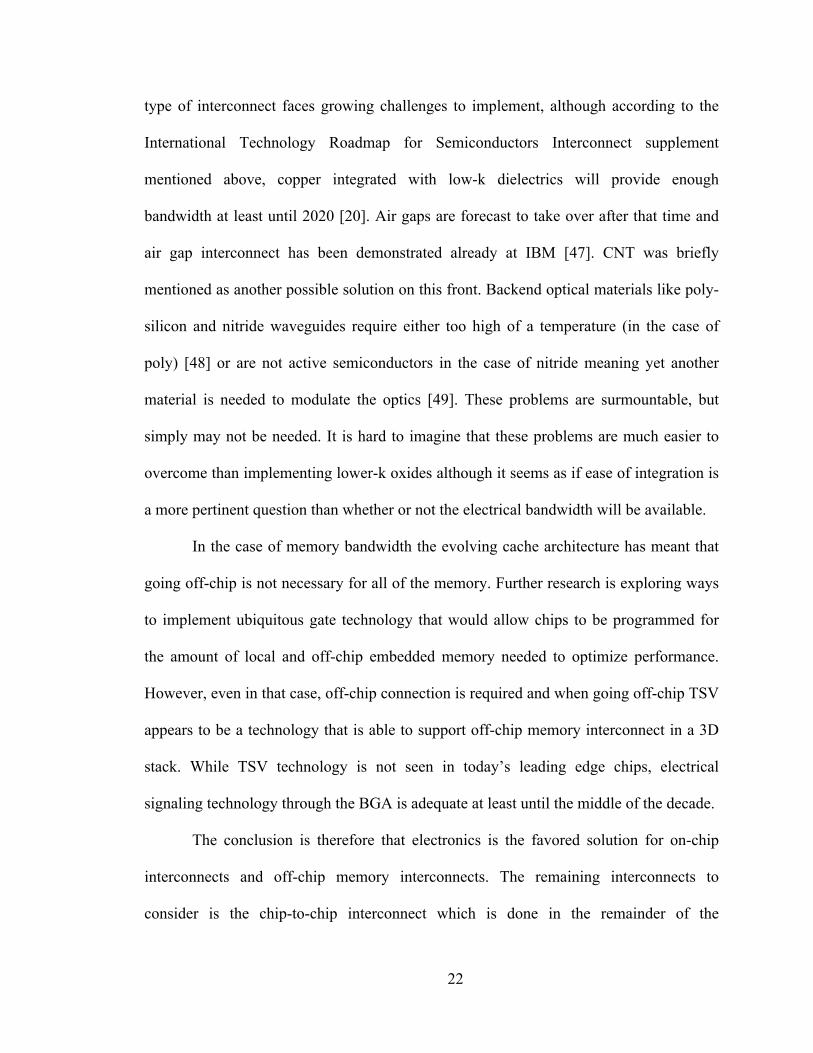
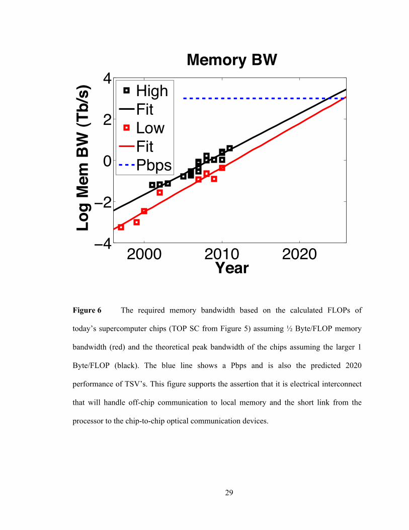
To do this calculation the larger SC-FLOPS from actual supercomputers
combined with the requisite 0.5 Bytes/FLOP, 4bits/FLOP, will be used to discern the
lower bound of the memory bandwidth requirement. Multiplying the higher 1Byte/FLOP,
8 bits/FLOP, times the theoretical peak of the chips will serve as the upper bound and the
results can be found in Figure 6. The difference is large, but becomes less significant
against the bandwidth that TSV’s can conservatively provide which is demonstrated in
Figure 7.
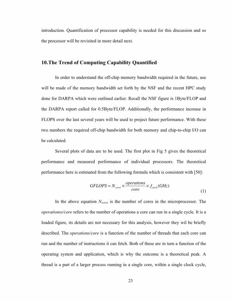
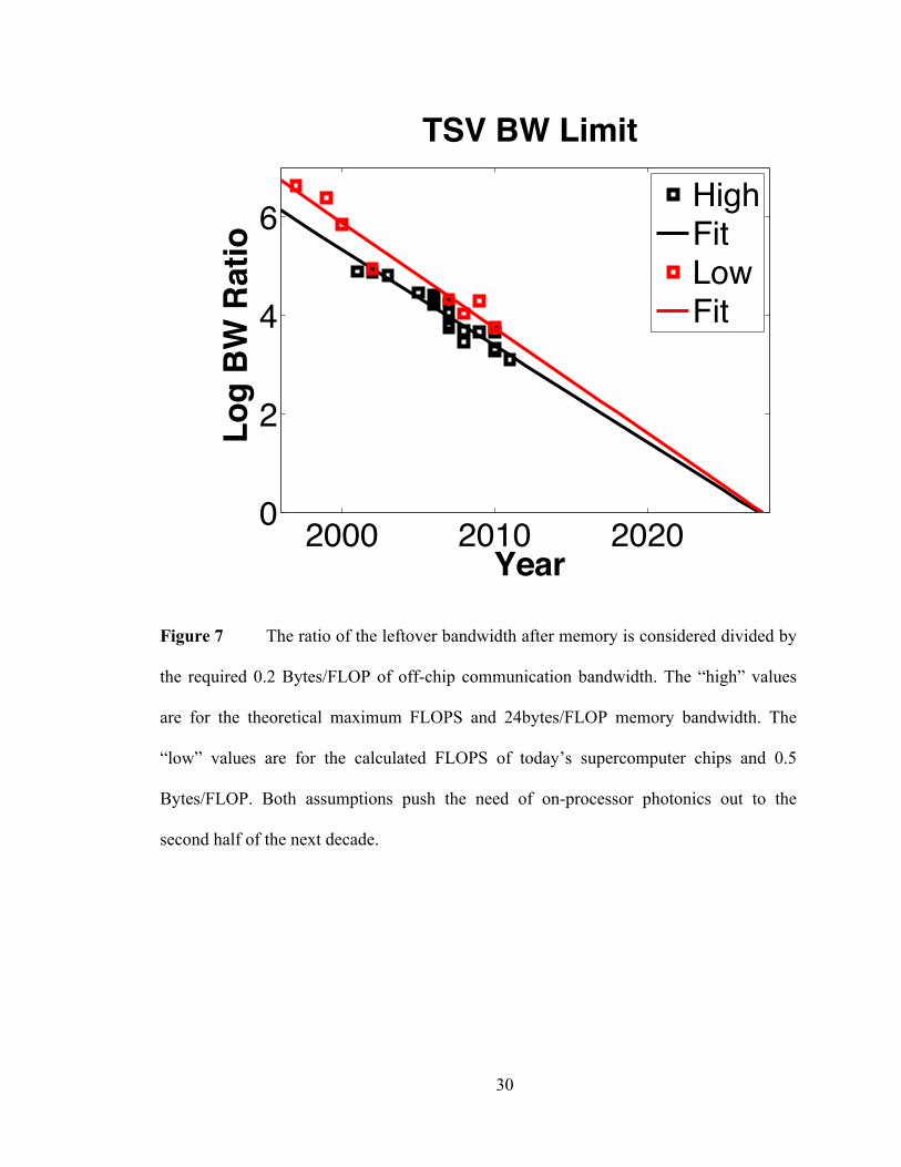
Figure 7 shows the result of the following calculation for the low and high
memory bandwidth scenarios:
R =(1pbit ! BWM )
( bytesFLOP
" bitsbyte
" FLOPS) (2)
Here all values are in units of peta-bits or peta-FLOPS. BWm is the memory bandwidth
and FLOPS refers to the chip’s performance. The variables BW and FLOPS change based
on the intent to calculate the high or low bandwidth requirement. The value for
bytes/FLOP in the denominator come from the same NSF study that was quoted earlier
outlines a chip-to-chip link BW of 0.2B/Flop. The bits/byte is defined as eight. This
figure is also specified in the Blue Waters system so it has both theoretical and
demonstrated support as a valid figure [2, 14, 16]. The figure of merit R then represents
the ratio of bandwidth remaining after the memory is satisfied divided by the required
chip-to-chip bandwidth. As long as the value is greater than one, chip-to-chip
interconnect does not need to originate on processor and there is no need for optical
28
monolithic integration onto the chip. This equation would be broadly useful for any
system, but TSV’s are chosen because they are the most likely off-chip interconnect for
future systems. Therefore in Figure 7, where the lines intersect with one on the Y-axis (0
for the log scale) is where the TSV array at 1Pbps is completely saturated with memory
and chip-to-chip bandwidth. It is clear that TSV technology offers so much bandwidth
that optical interconnects for chip-to-chip communication can be off-processor.
29
Figure 6 The required memory bandwidth based on the calculated FLOPs of
today’s supercomputer chips (TOP SC from Figure 5) assuming ½ Byte/FLOP memory
bandwidth (red) and the theoretical peak bandwidth of the chips assuming the larger 1
Byte/FLOP (black). The blue line shows a Pbps and is also the predicted 2020
performance of TSV’s. This figure supports the assertion that it is electrical interconnect
that will handle off-chip communication to local memory and the short link from the
processor to the chip-to-chip optical communication devices.
2000 2010 20204
2
0
2
4
Year
Log
Mem
BW
(Tb/
s) Memory BW
HighFitLowFitPbps
30
Figure 7 The ratio of the leftover bandwidth after memory is considered divided by
the required 0.2 Bytes/FLOP of off-chip communication bandwidth. The “high” values
are for the theoretical maximum FLOPS and 24bytes/FLOP memory bandwidth. The
“low” values are for the calculated FLOPS of today’s supercomputer chips and 0.5
Bytes/FLOP. Both assumptions push the need of on-processor photonics out to the
second half of the next decade.
2000 2010 20200
2
4
6
Year
Log
BW
Rat
io
TSV BW Limit
HighFitLowFit
31
11. Chip-to-Chip Interconnect
Based on the outcome of the last section the final area to explore is the type of
optical interconnects to incorporate onto the 3D stack. The chip-to-chip interconnect for a
large-scale machine is the other large piece of off-chip bandwidth.
The simple and effective answer for these types of interconnect has been VCSEL
technology. VCSEL’s provide high bandwidth and the promise of even higher bandwidth
in the future. However, a shortcoming of VCSEL technology is that its multiplexing
ability is limited. The lack of multiplexing will, at some point result in a WDM scheme
overtaking VCSEL’s as the choice for HPC interconnect. The scale that will tip in favor
of WDM may be the number of fibers needed to connect enough VCLS to a single chip.
VCSEL technology that takes advantage of double intra-cavity oxide confinement
architecture is a high bandwidth, low power and reliable choice for large machine
interconnect. Recently UCSB [51] demonstrated a 35Gbps data rate with as little as
286fJ/bit in a 980nm VCSEL. The VCSEL in this paper can achieve even lower E/bit at
lower data rates. Imai et al demonstrated a data rate of 10Gbps at 1060nm using 140fJ/bit
and showed that over 5000 hours of cycling after thermal and humidity stress these
devices could maintain output power within 10% of the original after burn in [52].
Additionally VCSEL’s operating at 1550nm have been demonstrated and even show
promise for data center virtualization and transparency with optical injection locking
(OIL) enabling negative chirp and 3dB power penalty out to 90Km [53]. VCSEL
technology, which has been the mainstay of chip-to-chip interconnect for ten years, has
the fundamental capabilities to continue. However, as mentioned already, VCSEL
technology today is fundamentally single channel per fiber parallel technology.

32
Consider a 10 TFLOP chip, which is projected for 2018 based on Figure 5. A
Teraflop would require 16Tbps of chip-to-chip bandwidth (FLOPS X 1.6 bits/FLOP). If
the assumed VCSEL bandwidth at that time were 50Gbps, which is more than 25%
increase over today’s top research devices, then 320 VCSEL’s would be required per
chip. IBM Blue Waters uses 10 VCSEL’s per chip (40 VSCELs connected to a 4 chip
hub). This would require multiplexing the 1Gbps TSV line forty times and intimate
VCSEL integration with CMOS on the optical chip (not demonstrated). Demultiplexing
in the receiver will also add to the power and complexity of the receiver circuitry.
Additionally, if a 3D chip stack were used then designers would lose a degree of
freedom. The vertical cavity implies that the optical chip must be on top.
A further issue with, say an exascale machine in 2018, is that based on Figure 5
chips will be running at 10TFLOPS. To run at an EFLOP the machine will need 100,000
processors. If each processor requires 320 optical lines (using the 50Gbps VCSEL) this is
32 million fibers and VCSEL’s in a machine of this size.
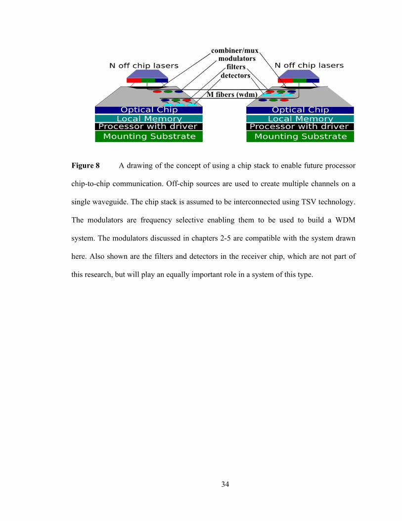
The alternative proposed here is a silicon photonic WDM system operating in the
C band on a 50GHz channel spacing that could provide 75 channels per fiber. This
concept is drawn in Figure 8. Extending the system into the L-band can easily double
this. A system running at the TSV bandwidth of 1Pbps would require 16000 channels or
210 fibers per chip on a 75-channel system. If amplification is not necessary, which in a
warehouse sized building it may not be, then more channels can be selected outside of the
typical range of C and L-band erbium doped fiber amplifiers (EDFA). Multiplexing will
be available for silicon photonics on the same substrate using monolithic integration with
CMOS so the fiber count can be reduced as needed. In this work monolithic integration
33
with 2GHz CMOS is demonstrated as in Zortman et. al. [54] in chapter 3 with the speed
only limited by the .35µm technology that was used. With multiplexing just to 10Gbps
the fiber count drops to 21 per chip and 200,000 in an exascale machine. Furthermore, the
nature of integrated silicon waveguides means that edge fiber coupling is possible,
allowing greater design freedom for the chip stack.
With silicon photonics as a seemingly effective WDM solution for HPC
applications and the capability of TSV technology to provide the off-chip bandwidth well
into the next decade, the crystalline silicon can be used to fabricate devices which is
consistent with the research presented in the subsequent chapters. This is important
because other silicon photonic demonstrations using backend processing have higher
optical loss and furthermore no mechanism to integrate the high temperatures of backend
poly-silicon with front-end transistor technology is known without causing the diffusion
of source and drain dopants during the 600oC poly-silicon deposition process.
34
Figure 8 A drawing of the concept of using a chip stack to enable future processor
chip-to-chip communication. Off-chip sources are used to create multiple channels on a
single waveguide. The chip stack is assumed to be interconnected using TSV technology.
The modulators are frequency selective enabling them to be used to build a WDM
system. The modulators discussed in chapters 2-5 are compatible with the system drawn
here. Also shown are the filters and detectors in the receiver chip, which are not part of
this research, but will play an equally important role in a system of this type.
35
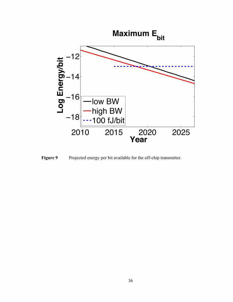
12. A Note on The Energy per Bit
The energy per bit is a figure of merit that is important because most
microprocessor architectures are limited to 100W/cm2 and in a 2cm2 chip, which is on the
large end, this would be 200W. It is estimated that about 20% of the chip’s power will be
available for off-chip interconnection [14]. It is unknown how much is allocated for the
receiver and how much for the transmitter, but it will be assumed that each gets half. If
this is the case then a maximum of 20W can be expected and if the total off-chip
bandwidth is the memory plus the chip-to-chip communication it is easy to plot these
requirements, which is done in Figure 9. The plot is the result of dividing the sum of the
bandwidth into 20W. The bandwidth sum is the projected supercomputer FLOPS per chip
(green in Figure 5) times 5.6 bits/FLOP (0.5B for memory and 0.2B for chip-to-chip).
The red line is the same calculation done for a B/FLOP using the theoretical peak of the
processors. It is useful to keep these values in mind because they are an upper bound on
the energy per bit any modulator can exhibit. It is noted that today’s best VCSEL’s
remain under the red curve until the end of this decade.
36
Figure 9 Projected energy per bit available for the off-chip transmitter.
2010 2015 2020 2025
18
16
14
12
Year
Log
Ene
rgy/
bit
Maximum Ebit
low BWhigh BW100 fJ/bit
37
13. Summary and Overview of Subsequent Chapters
The silicon photonic transmitter technology that will be discussed is low power,
high speed, manufacturable, compatible with differential signaling and CMOS processing
and capable of enabling data center virtualization through its measured long haul
characteristics.
In a continuing age where chip-processing power continues to exponentially
increase, engineers have continually found ways to surmount the barriers that this
progress generates. Transistor densities continue to scale through the use of new
materials and processes. Where chip power dissipation reached a wall, multiple cores
were instituted to enable the solving of more complex problems. Innovations in low-k
dielectrics allow metal interconnect to scale against otherwise debilitating parasitics.
Faster chips require faster access to memory to feed processing cores with adequate data
and along with that, in large machines, the chip-to-chip interconnect bandwidth
requirement continues to scale.
The purpose of this introduction was to pose the problem and illuminate the
relevant solutions to the memory bandwidth and chip-to-chip interconnect requirements.
Memory bandwidth is clearly the largest consumer of communication resources, but new
3D integration technology, TSV’s in particular, will provide enough bandwidth to allow
excess room for integration of optics on a chip other than the processor. In addition, the
developments in memory architecture continue to reduce the need for off-chip memory
bandwidth.
With the freedom to look at off-processor solutions to this problem, two
candidates for optical chip-to-chip communication were examined. The first was VCSEL
38
technology, which offers the necessary bandwidth. The key limitation of VCSEL’s is that
they do not optically multiplex easily and even with electrical multiplexing require
inordinate amounts of fiber to work. Silicon photonics offers the ability to multiplex and
integration with monolithic CMOS and with that can provide the bandwidth for chips
projected later in the decade while keeping fiber requirements to a minimum.
There are two conclusions reached from the analysis of the larger systems that
optical communications support in the case of HPC. The first is that the optics is off chip.
In a silicon photonic solution this is important because it means that the crystalline silicon
lattice can be utilized on the photonic chip enabling the low loss waveguides and
resonators presented in the subsequent chapters. The other outcome is that a low power
WDM solution is almost certainly required for off chip communications in HPC systems
to enable Exaflop machines sometime near 2018. The remainder of this dissertation
demonstrates a modulator that fulfills the low power WDM requirement and has been
fabricated in the silicon crystalline lattice.
In Chapter 2 the lower power and low voltage capability of the modulator will be
demonstrated including differential signaling compatible with common CMOS standards.
The low power capability has been demonstrated by Zortman et al in [55] and is the
lowest power and voltage of any modulator of any type to the best of the author’s
knowledge. The modulation energy per bit is only 3fJ using single ended electrical
connection. Using differential signaling, energy as low as 1fJ/bit is demonstrated. This
capability means that the modulation energy is essentially negligible and that the
modulators are compatible with every known or proposed low voltage signaling
39
technology. The power and electrical integration are therefore straightforward with this
technology.
The next compatibility demonstration is done in Chapter 3 and can also be
reviewed in associated work by Zortman [54]. Chapter 3 covers monolithic and 2D
integration with CMOS. The modulator works in both integration schemes. Most
demonstrative of silicon photonics technological compatibility is the ease in which a
silicon photonic modulator can be dropped into a running CMOS process. Further, the
monolithic demonstration shows that drivers can be integrated on the photonic chip. This
has more implication on the receiver. Although, the receiver is not covered in this work,
electronics will be needed to convert the detector current to a voltage signal. The ease of
monolithic integration shows that this is at least possible with other varieties of silicon
photonic devices.
In Chapter 4 the manufacturability of these parts is investigated with particular
attention paid to the uniformity and the impact this has on the power budget. Zortman
first published this in [56, 57]. In Chapter 2 the modulation part of the power budget is
demonstrated to be inconsequential with this technology. Chapter 4 explores in detail
another part of that power budget which is the power required to actively correct
manufacturing non-uniformity. The power to compensate for environmental temperature
change is also quantified at the end of chapter 4 so that a final picture of the power
budget is realized.
Finally, Chapter 5 further explores the versatility of the part with long haul
characterization and modeling, which was reported by Zortman in [58, 59]. This is not a
critical capability for a supercomputer, but could enable a simpler regime for virtualizing
40
datacenters. Data center operators would have the freedom to link chips that are
geographically separated using the same optics that are used for the short haul links.
The report on research starts with the architecture, energy and bandwidth
performance of the modulator and builds up from there to show how this demonstrated
performance interfaces with CMOS signaling, CMOS processing and integration into
large systems built with CMOS chips. As stated at the beginning of this chapter, a silicon
photonic modulator which fulfills the future requirements of chip-to-chip, is described
and demonstrated in this dissertation.
14. References
1. Ferris-Prabhu, A.V., Introduction to Semiconductor Device Yield Modeling1992, New York: Artech House.
2. (editor), P.M.K., Exascale Computing Study: Technology Challenges in Achieving Exascale Systems. University of Notre Dame CSE Department, 2008(TR-2008-13).
3. Chen, F., et al. Line edge roughness and spacing effect on low-k TDDB characteristics. in Reliability Physics Symposium, 2008. IRPS 2008. IEEE International. 2008.
4. Chen, X., et al. A cost effective 32nm high-K/ metal gate CMOS technology for low power applications with single-metal/gate-first process. in VLSI Technology, 2008 Symposium on. 2008.
5. Jan, C.H., et al. A 32nm SoC platform technology with 2<sup>nd</sup> generation high-k/metal gate transistors optimized for ultra low power, high performance, and high density product applications. in Electron Devices Meeting (IEDM), 2009 IEEE International. 2009.
6. Wang, X., L. Wu, and Y. Liu, Low-power LVDS I/O interface for above 2Gb/s-per-pin operation. Journal of Electronics (China), 2009. 26(4): p. 525-531.
7. Zhang, W., N.K. Jha, and L. Shang, Design space exploration and data memory architecture design for a hybrid nano/CMOS dynamically reconfigurable architecture. J. Emerg. Technol. Comput. Syst., 2009. 5(4): p. 1-27.
8. Sinharoy, B. POWER7 multi-core processor design. in Microarchitecture, 2009. MICRO-42. 42nd Annual IEEE/ACM International Symposium on. 2009.
9. Howard, J., et al., A 48-Core IA-32 Processor in 45 nm CMOS Using On-Die Message-Passing and DVFS for Performance and Power Scaling. Solid-State Circuits, IEEE Journal of, 2011. 46(1): p. 173-183.

41
10. Kogge, P., The Tops in Flops (vol 48, pg 48, 2011). Ieee Spectrum, 2011. 48(3): p. 8-8.
11. Kwong, J. and A.P. Chandrakasan, Advances in Ultra-Low-Voltage Design. Solid-State Circuits Newsletter, IEEE, 2008. 13(4): p. 20-27.
12. Kaul, H., et al., A 320 mV 56 μW 411 GOPS/Watt Ultra-Low Voltage Motion Estimation Accelerator in 65 nm CMOS. Solid-State Circuits, IEEE Journal of, 2009. 44(1): p. 107-114.
13. Borkar, S. The Exascale challenge. in VLSI Design Automation and Test (VLSI-DAT), 2010 International Symposium on. 2010.
14. Miller, D.A.B., Device Requirements for Optical Interconnects to Silicon Chips. Proceedings of the IEEE, 2009. 97(7): p. 1166-1185.
15. Daniel E. Atkins, K.K.D., Stuart I. Feldman, Hector Gacia-Molina, Michael L. Klein, David G. Messerschmitt, Paul Messina, Jeremiah P. Ostriker, Margaret H. Wright, Revolutionizing Science and Engineering Through Cyberinfrastructure. Report on the National Science Foundation Blue-Ribbon Advisory Panel on Cyberinfrastructure, 2003.
16. Blue Waters Sustained Petascale Computing. http://www.ncsa.illinois.edu/BlueWaters/system.html
17. John, E.C., et al. Scaling VCSEL Reliability Up to 250Terabits/s of System Bandwidth. 2005. Optical Society of America.
18. Hino, T., et al. A 10 Gbps x 12 channel pluggable optical transceiver for high-speed interconnections. in Electronic Components and Technology Conference, 2008. ECTC 2008. 58th. 2008.
19. ; Available from: http://www.qdpma.com/CPU/CPU_Nehalem.html. 20. International Technology Roadmap for Semiconductors 2009 Edition -
Interconnect. 21. Amdahl, G.M., Validity of the single processor approach to achieving large scale
computing capabilities. AFIPS Joint Computer Conference, 1967. 22. Hill, M.D. and M.R. Marty, Amdahl's law in the multicore era. Computer, 2008.
41(7): p. 33-+. 23. Rattner, J., The dawn of terascale computing. Solid-State Circuits Magazine,
IEEE, 2009. 1(1): p. 83-89. 24. Rattner, J. Intel Two Terflop Chip: Terascale Project. Intel Developer Forum
2007; Available from: http://www.macworld.com/article/57395/2007/04/2tflops.html.
25. Seiler, L., et al., Larrabee: a many-core x86 architecture for visual computing. ACM Trans. Graph., 2008. 27(3): p. 1-15.
26. Kongetira, P., K. Aingaran, and K. Olukotun, Niagara: a 32-way multithreaded Sparc processor. Micro, IEEE, 2005. 25(2): p. 21-29.
27. Xie, Y., et al., Design space exploration for 3D architectures. J. Emerg. Technol. Comput. Syst., 2006. 2(2): p. 65-103.
28. Facchini, M., et al., An RDL-configurable 3D memory tier to replace on-chip SRAM, in Proceedings of the Conference on Design, Automation and Test in Europe2010, European Design and Automation Association: Dresden, Germany. p. 291-294.
42
29. Krishnamoorthy, A.V., et al., Computer Systems Based on Silicon Photonic Interconnects. Proceedings of the IEEE, 2009. 97(7): p. 1337-1361.
30. Kawano, M., et al. A 3D Packaging Technology for 4 Gbit Stacked DRAM with 3 Gbps Data Transfer. in Electron Devices Meeting, 2006. IEDM '06. International. 2006.
31. Marchal, P., et al. Verifying thermal/thermo-mechanical behavior of a 3D stack — challenges and solutions. in VLSI Technology Systems and Applications (VLSI-TSA), 2010 International Symposium on. 2010.
32. Kim, Y.J., et al., Thermal Characterization of Interlayer Microfluidic Cooling of Three-Dimensional Integrated Circuits With Nonuniform Heat Flux. Journal of Heat Transfer, 2010. 132(4): p. 041009-9.
33. Weldezion, A.a.W., Roshan and Pamunuwa, Danesh B. and Zheng, Li-Rong and Tenhunen, Hannu (2009) Bandwidth optimization for through silicon via (TSV) bundles in 3D integrated circuits. In: Workshop Notes, Design, Automation and Test in Europe.
34. Bermond, C., et al. High frequency characterization and modeling of high density TSV in 3D integrated circuits. in Signal Propagation on Interconnects, 2009. SPI '09. IEEE Workshop on. 2009.
35. Koyanagi, M., T. Fukushima, and T. Tanaka, High-Density Through Silicon Vias for 3-D LSIs. Proceedings of the IEEE, 2009. 97(1): p. 49-59.
36. Savidis, I. and E.G. Friedman, Closed-Form Expressions of 3-D Via Resistance, Inductance, and Capacitance. Electron Devices, IEEE Transactions on, 2009. 56(9): p. 1873-1881.
37. Bernstein, K., et al., Interconnects in the third dimension: design challenges for 3D ICs, in Proceedings of the 44th annual Design Automation Conference2007, ACM: San Diego, California. p. 562-567.
38. Brewer, J.E., V.V. Zhirnov, and J.A. Hutchby, Memory technology for post CMOS era. Circuits and Devices Magazine, IEEE, 2005. 21(2): p. 13-20.
39. Ki Chul, C., P. Jain, and C.H. Kim. Logic-compatible embedded DRAM design for memory intensive low power systems. in Circuits and Systems (ISCAS), Proceedings of 2010 IEEE International Symposium on. 2010.
40. Natarajan, S., et al., Searching for the dream embedded memory. Solid-State Circuits Magazine, IEEE, 2009. 1(3): p. 34-44.
41. Chen, F., et al., Scaling and evaluation of carbon nanotube interconnects for VLSI applications, in Proceedings of the 2nd international conference on Nano-Networks2007, ICST (Institute for Computer Sciences, Social-Informatics and Telecommunications Engineering): Catania, Italy. p. 1-8.
42. Calarnia, J., Can Carbon Put Copper Down for the Count? IEEE Spectrum, 2010. 47(December): p. 9-10.
43. An Introduction to the Intel QuickPath Interconnect, 2009. 44. Intel Itanium Processor 9300 Series, 2010. 45. Byungsub, K. and V. Stojanovic. A 4Gb/s/ch 356fJ/b 10mm equalized on-chip
interconnect with nonlinear charge-injecting transmit filter and transimpedance receiver in 90nm CMOS. in Solid-State Circuits Conference - Digest of Technical Papers, 2009. ISSCC 2009. IEEE International. 2009.
43
46. Dally, W.J. and J. Poulton, Transmitter equalization for 4-Gbps signaling. Micro, IEEE, 1997. 17(1): p. 48-56.
47. Nitta, S., et al. Performance and reliability of airgaps for advanced BEOL Interconnects. in Interconnect Technology Conference, 2008. IITC 2008. International. 2008.
48. Preston, K., B. Schmidt, and M. Lipson, Polysilicon photonic resonators for large-scale 3D integration of optical networks. Opt. Express, 2007. 15(25): p. 17283-17290.
49. Young, I.A., et al. Integration of nano-photonic devices for CMOS chip-to-chip optical I/O. in Lasers and Electro-Optics (CLEO) and Quantum Electronics and Laser Science Conference (QELS), 2010 Conference on. 2010.
50. Samuel Williams, K.D., Jonathan Carter, Leonid Oliker, John Shalf, Katherine Yelick , David Bailey, PERI - auto-tuning memory-intensive kernels for multicore. Journal of Physics, 2008. 125.
51. Chang, Y.C., C.S. Wang, and L.A. Coldren, High-efficiency, high-speed VCSELs with 35 Gbit=s error-free operation. Electronics Letters, 2007. 43(19): p. 1022-1023.
52. Imai, S., et al. Recorded low power dissipation of 0.14 mW/Gbps in 1060 nm VCSELs for “Green” optical interconnection. in Semiconductor Laser Conference (ISLC), 2010 22nd IEEE International. 2010.
53. Bo, Z., et al. Adjustable Chirp Injection-Locked 1.55-μm VCSELs for Enhanced Chromatic Dispersion Compensation at 10-Gbit/s. in Optical Fiber communication/National Fiber Optic Engineers Conference, 2008. OFC/NFOEC 2008. Conference on. 2008.
54. Zortman, W.A., et al. Monolithic integration of silicon electronics and photonics. in Winter Topicals (WTM), 2011 IEEE. 2011.
55. Zortman, W.A., et al. Low-power high-speed silicon microdisk modulators. in Lasers and Electro-Optics (CLEO) and Quantum Electronics and Laser Science Conference (QELS), 2010 Conference on. 2010.
56. William, A.Z., R.W. Michael, and C.T. Douglas. Determination of Wafer and Process Induced Resonant Frequency Variation in Silicon Microdisk-Resonators. 2009. Optical Society of America.
57. Zortman, W.A., D.C. Trotter, and M.R. Watts, Silicon photonics manufacturing. Opt. Express, 2010. 18(23): p. 23598-23607.
58. Zortman, W.A., et al. Power penalty measurement and frequency chirp extraction in silicon microdisk resonator modulators. in Optical Fiber Communication (OFC), collocated National Fiber Optic Engineers Conference, 2010 Conference on (OFC/NFOEC). 2010.
59. Zortman, W., et al., Long Distance Demonstration and Modeling of Low-Power Silicon Microdisk Modulators. Photonics Technology Letters, IEEE, 2011. PP(99): p. 1-1.
44
Chapter Two: Low Voltage Bias and
Differential Signaling of a Low Power High
Speed Modulator
1. Introduction
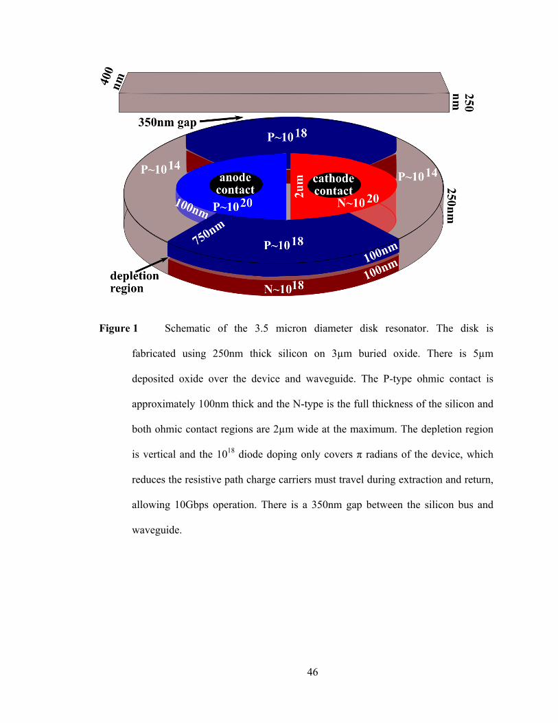
Microdisk resonators have been proposed for high speed and low energy optical
interconnect integration with CMOS electronics. Silicon photonic optical modulators
with speeds up to 10Gb/s and energy as low as 50fJ/bit have been reported and recent
demonstrations of ring and disk silicon micro-resonators continue to build the case for
these devices as compact, low power and high-speed solutions for chip to chip
interconnect [1-9]. The modulator presented here demonstrates both increased bandwidth
and reduced power dissipation by further reducing the physical size, introducing new
doping geometry and reducing the applied voltage from a small negative to a small
positive voltage that is less than the built-in potential of the device.

45
2. Analysis
The bandwidth limitation in reverse biased depletion mode modulators is
currently driven by the RC time constant. Likewise, the energy consumption of the
reverse biased modulator can be decreased through reduced capacitance leading to
smaller devices. Speed increases and energy savings can be gained by making the active
PN junction region as small as possible through selective doping of the modulator
periphery as in Figure 1. This modulator is a 3.5µm disk contacted near the center as in
previous designs [6]. However, in this design, the PN diode is only implanted around the
periphery of the device limiting junction capacitance to that area. The charge must be
extracted by following this same peripheral line, which is a limitation when the PN
junction doping goes around the entire 2π radians of the disk. However, by limiting the
doping to only π radians of the device, resistance is cut in half allowing for higher speed
operation. Decreasing dopant-induced loss also increases the Q of the device. This results
in a smaller required shift to get the necessary extinction for BER<10-12 operation. Even
though the index shift, δn/n, is in theory only half as much as if the device was doped
over 2π radians, at high-speed larger devices do not fully deplete the charge in such a
large area as a result of the increased resistance and capacitance. In effect, a device that is
completely peripherally doped cannot take advantage of the index shift around the
46
Figure 1 Schematic of the 3.5 micron diameter disk resonator. The disk is
fabricated using 250nm thick silicon on 3µm buried oxide. There is 5µm
deposited oxide over the device and waveguide. The P-type ohmic contact is
approximately 100nm thick and the N-type is the full thickness of the silicon and
both ohmic contact regions are 2µm wide at the maximum. The depletion region
is vertical and the 1018 diode doping only covers π radians of the device, which
reduces the resistive path charge carriers must travel during extraction and return,
allowing 10Gbps operation. There is a 350nm gap between the silicon bus and
waveguide.
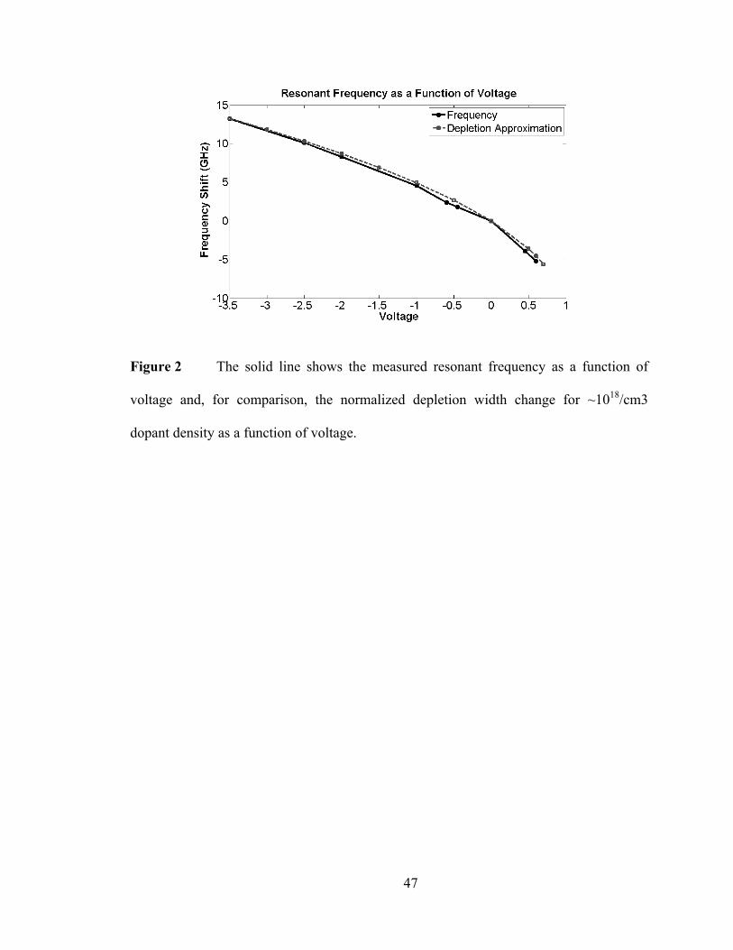
47
Figure 2 The solid line shows the measured resonant frequency as a function of
voltage and, for comparison, the normalized depletion width change for ~1018/cm3
dopant density as a function of voltage.
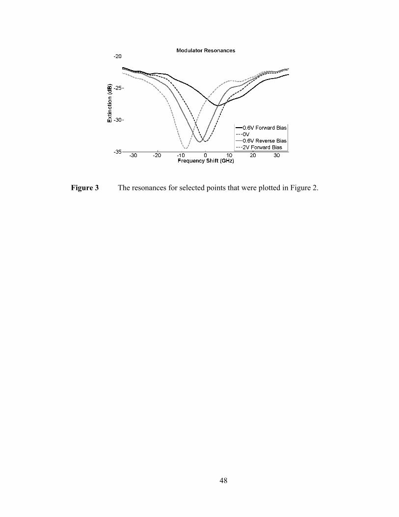
48
Figure 3 The resonances for selected points that were plotted in Figure 2.

49
entire device at high speed and by only doping half of the disk, the free-carrier optical
losses are reduced, enabling higher-Q resonances.
The method used to drive the device reduces the drive voltage and therefore, the
consumed energy-per-bit. Devices driven in forward bias are usually bandwidth limited
by the carrier lifetime in the depletion region and pass current 50% of the time in a non
return to zero coding scheme. Reverse bias devices are limited by carrier sweep out times
from the depletion region, which is a much faster effect. However, larger voltages (2.5V
– 3.5V) are required to move enough charge from the neutral region to create a suitable
index shift. From the depletion approximation it is known that the depletion region
widens as the square root of voltage so each incremental voltage shift in the reverse bias
results in less effect. However, by driving the modulator slightly into the forward bias,
but below the built in potential, the depletion region is reduced (charge is stored), but
little current is passed. In this mode of operation a larger amount of charge is moved with
smaller shifts in voltage compared to a reverse biased device, but the speed of response is
not limited by the carrier lifetime because sub-turn-on voltage allows the persistence of a
built in field similar to a reverse biased device. The capacitance of the device is increased
over what it would be if the device were operated only in reverse bias, but the carrier
concentration change (and thereby index change) is the same in either case for a given
shift in the resonance. Because the energy per bit is E=CV2/4, driving down the required
voltage more than offsets the slightly increased capacitance enabling a significant
reduction in energy-per-bit. Figure 2 shows this process as it generates the plasma-optic
index shift [10] resulting from depletion region widening (charge extraction). The
depletion region expansion for 1.2 V shift from 0.6V to -0.6V results in a frequency shift
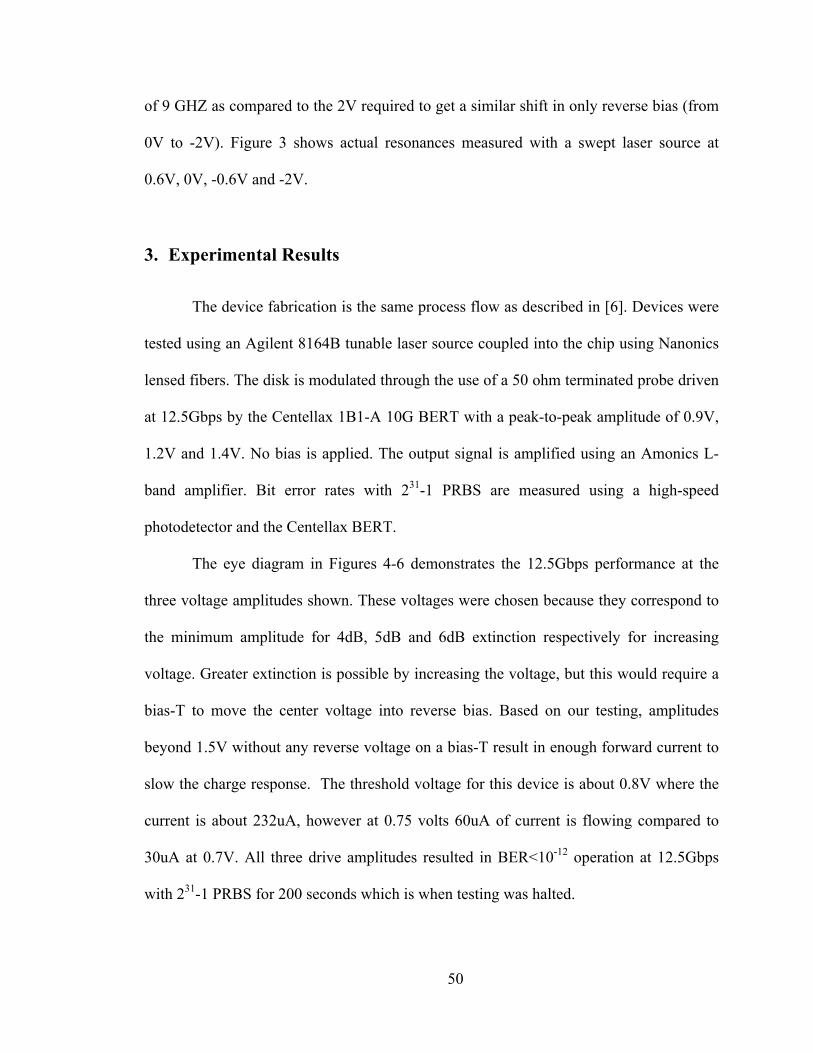
50
of 9 GHZ as compared to the 2V required to get a similar shift in only reverse bias (from
0V to -2V). Figure 3 shows actual resonances measured with a swept laser source at
0.6V, 0V, -0.6V and -2V.
3. Experimental Results
The device fabrication is the same process flow as described in [6]. Devices were
tested using an Agilent 8164B tunable laser source coupled into the chip using Nanonics
lensed fibers. The disk is modulated through the use of a 50 ohm terminated probe driven
at 12.5Gbps by the Centellax 1B1-A 10G BERT with a peak-to-peak amplitude of 0.9V,
1.2V and 1.4V. No bias is applied. The output signal is amplified using an Amonics L-
band amplifier. Bit error rates with 231-1 PRBS are measured using a high-speed
photodetector and the Centellax BERT.
The eye diagram in Figures 4-6 demonstrates the 12.5Gbps performance at the
three voltage amplitudes shown. These voltages were chosen because they correspond to
the minimum amplitude for 4dB, 5dB and 6dB extinction respectively for increasing
voltage. Greater extinction is possible by increasing the voltage, but this would require a
bias-T to move the center voltage into reverse bias. Based on our testing, amplitudes
beyond 1.5V without any reverse voltage on a bias-T result in enough forward current to
slow the charge response. The threshold voltage for this device is about 0.8V where the
current is about 232uA, however at 0.75 volts 60uA of current is flowing compared to
30uA at 0.7V. All three drive amplitudes resulted in BER<10-12 operation at 12.5Gbps
with 231-1 PRBS for 200 seconds which is when testing was halted.

51
Energy measurements were done with Time Domain Reflectometry (TDR) on a
Tektronix DSA. For a drive amplitude of 1V (from 0.5 forward bias to 0.5 reverse bias)
the energy measured is 3fJ/bit. The TDR pulse is only available in 0.5V increments and
measurements at 0.75 volts are confounded by the presence of a more substantial (60uA)
sub-threshold current (The threshold here refers to the diode turn on and should not be
confused with the threshold voltage in a MOSFET). The results were compared to an
analytical model that uses the depletion approximation capacitance for the diode, ohmic
regions and fringes [11]. In that analysis room temperature was assumed, doping was
approximated at 1018 for both N and P type and the permittivity of silicon was used. The
analytical result of 3.8fJ/bit compares favorably with the measurement.
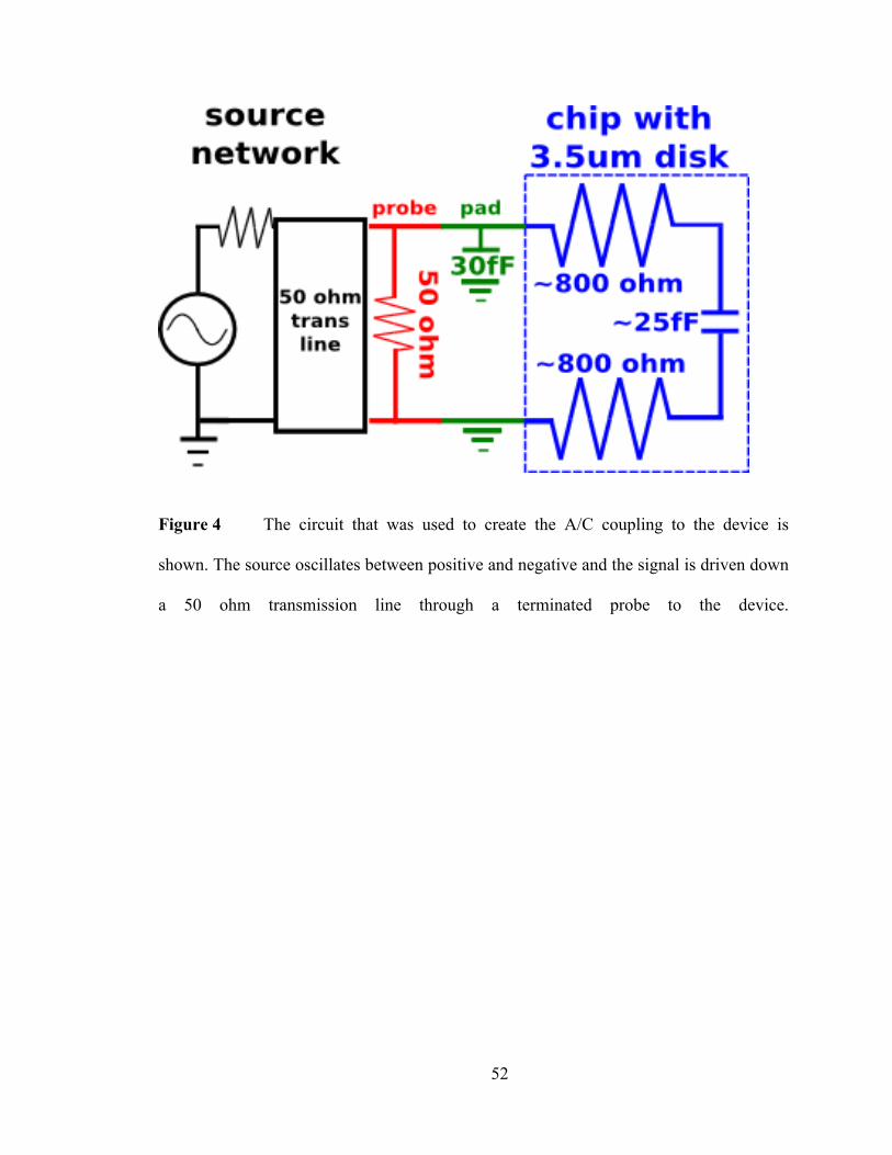
52
Figure 4 The circuit that was used to create the A/C coupling to the device is
shown. The source oscillates between positive and negative and the signal is driven down
a 50 ohm transmission line through a terminated probe to the device.
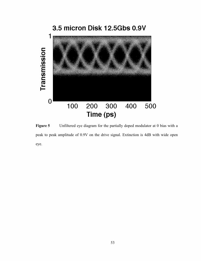
53
Figure 5 Unfiltered eye diagram for the partially doped modulator at 0 bias with a
peak to peak amplitude of 0.9V on the drive signal. Extinction is 4dB with wide open
eye.

54
Figure 6 The same modulator driven at 1.2V peak to peak amplitude and 0V bias
this time demonstrating 5dB of extinction.
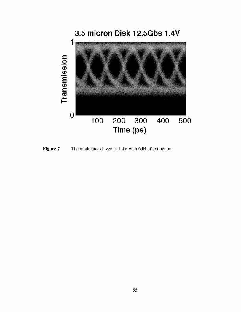
55
Figure 7 The modulator driven at 1.4V with 6dB of extinction.
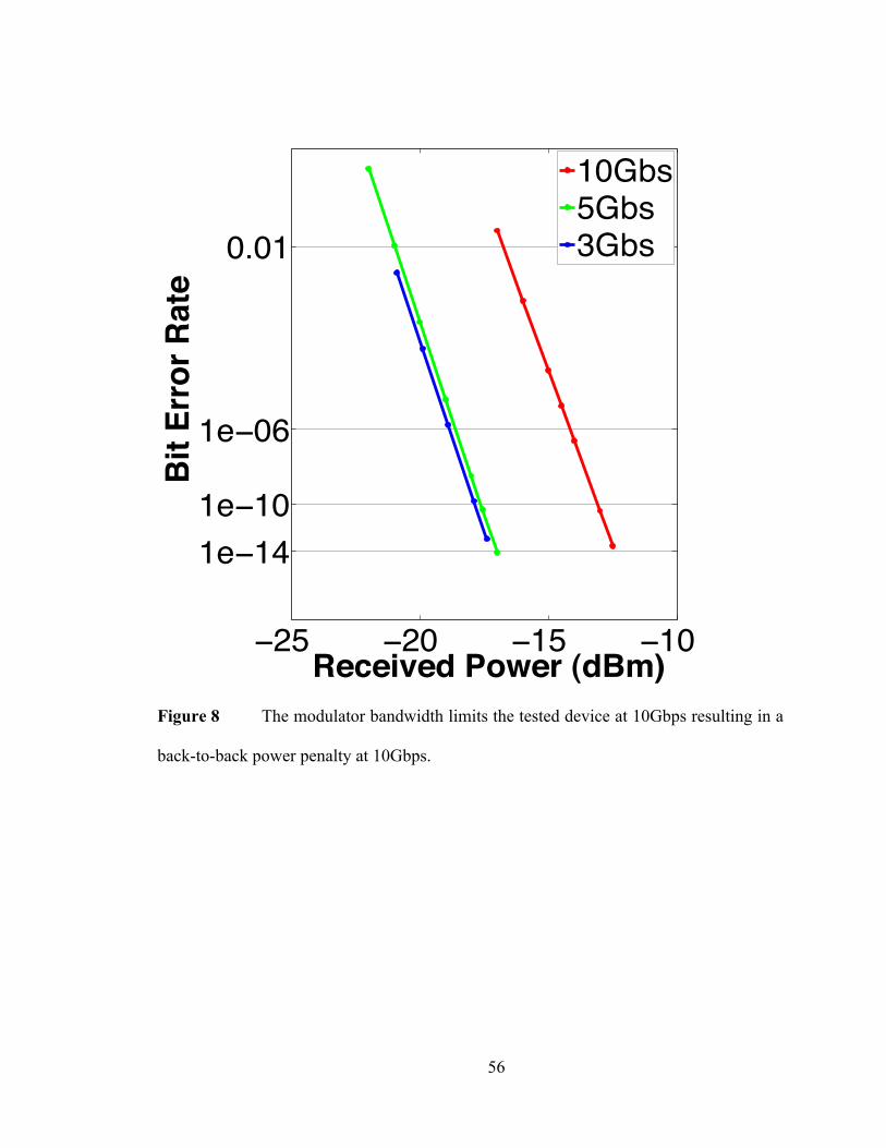
56
Figure 8 The modulator bandwidth limits the tested device at 10Gbps resulting in a
back-to-back power penalty at 10Gbps.
25 20 15 10
1e 141e 10
1e 06
0.01
Received Power (dBm)
Bit
Erro
r Rat
e
10Gbs5Gbs3Gbs

57
4. Conclusions on the Low Power Demonstration and a Note on BW
By shrinking the active region in a 3.5um silicon microdisk and introducing a new
bias regime, 12.5Gbs, 1V, BER<10-12 at 1V drive amplitude was achieved resulting in
energy performance of ~3 fJ/bit. These low voltage modulators can be driven directly at
logic-level from a CMOS chip, greatly simplifying CMOS modulator driver design,
which is explored next. In the foregoing demonstration a pattern running at 10Gbps is
used and, it will be seen, that the extinction ratio is greater in this case. This is because of
the inherent bandwidth limitation of a modulator of this type. The long PN junction
region around the periphery of the device introduces a resistance that limits the
bandwidth. The measured result can be seen in Figure 7.
5. Low Voltage Differentially Signaled Modulators
The efforts discussed so far demonstrate very low power consumption (and
energy per bit) as well as single volt drive which makes these devices compatible with
current complimentary metal oxide semiconductor (CMOS) chips. Even lower drive
voltages have been proposed in [12] for devices operating in forward bias although they
pull a direct current. The advantage of low drive voltage is that while the International
Technology Roadmap for Semiconductors (ITRS) does not predict Vdd levels to drop
below 700mV until at least 2024, recent work [13,14] has suggested that in order to
reduce power in exascale supercomputers to reasonable levels, transistor supply voltages
may need to be lower than ITRS predictions. 500mV chip supply rail levels are a
possibility and demonstrations have shown logic gates that can be run with Vdd as low as
350mV [15]. In order for optics to function with the low drive voltages proposed and the
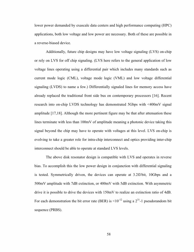
58
lower power demanded by exascale data centers and high performance computing (HPC)
applications, both low voltage and low power are necessary. Both of these are possible in
a reverse-biased device.
Additionally, future chip designs may have low voltage signaling (LVS) on-chip
or rely on LVS for off chip signaling. (LVS here refers to the general application of low
voltage lines operating using a differential pair which includes many standards such as
current mode logic (CML), voltage mode logic (VML) and low voltage differential
signaling (LVDS) to name a few.) Differentially signaled lines for memory access have
already replaced the traditional front side bus on contemporary processors [16]. Recent
research into on-chip LVDS technology has demonstrated 5Gbps with <400mV signal
amplitude [17,18]. Although the more pertinent figure may be that after attenuation these
lines terminate with less than 100mV of amplitude meaning a photonic device taking this
signal beyond the chip may have to operate with voltages at this level. LVS on-chip is
evolving to take a greater role for intra-chip interconnect and optics providing inter-chip
interconnect should be able to operate at standard LVS levels.
The above disk resonator design is compatible with LVS and operates in reverse
bias. To accomplish this the low power design in conjunction with differential signaling
is tested. Symmetrically driven, the devices can operate at 3.2fJ/bit, 10Gbps and a
500mV amplitude with 7dB extinction, or 400mV with 5dB extinction. With asymmetric
drive it is possible to drive the devices with 150mV to realize an extinction ratio of 4dB.
For each demonstration the bit error rate (BER) is <10-12 using a 231-1 pseudorandom bit
sequence (PRBS).

59
Figure 9 The equivalent circuit diagram of the differentially driven modulator
shows two identical drivers 180o out of phase connected through two different 50Ω
transmission lines to a high speed probe terminated with 50Ω. The contact pads have a
capacitance of 30fF and the modulator diode is a 25fF capacitor in series with 1600Ω of
resistance.
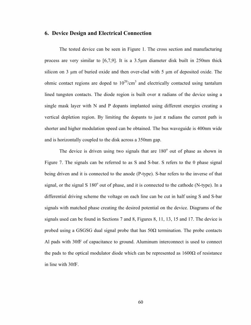
60
6. Device Design and Electrical Connection
The tested device can be seen in Figure 1. The cross section and manufacturing
process are very similar to [6,7,9]. It is a 3.5µm diameter disk built in 250nm thick
silicon on 3 µm of buried oxide and then over-clad with 5 µm of deposited oxide. The
ohmic contact regions are doped to 1020/cm3 and electrically contacted using tantalum
lined tungsten contacts. The diode region is built over π radians of the device using a
single mask layer with N and P dopants implanted using different energies creating a
vertical depletion region. By limiting the dopants to just π radians the current path is
shorter and higher modulation speed can be obtained. The bus waveguide is 400nm wide
and is horizontally coupled to the disk across a 350nm gap.
The device is driven using two signals that are 180o out of phase as shown in
Figure 7. The signals can be referred to as S and S-bar. S refers to the 0 phase signal
being driven and it is connected to the anode (P-type). S-bar refers to the inverse of that
signal, or the signal S 180o out of phase, and it is connected to the cathode (N-type). In a
differential driving scheme the voltage on each line can be cut in half using S and S-bar
signals with matched phase creating the desired potential on the device. Diagrams of the
signals used can be found in Sections 7 and 8, Figures 8, 11, 13, 15 and 17. The device is
probed using a GSGSG dual signal probe that has 50Ω termination. The probe contacts
Al pads with 30fF of capacitance to ground. Aluminum interconnect is used to connect
the pads to the optical modulator diode which can be represented as 1600Ω of resistance
in line with 30fF.
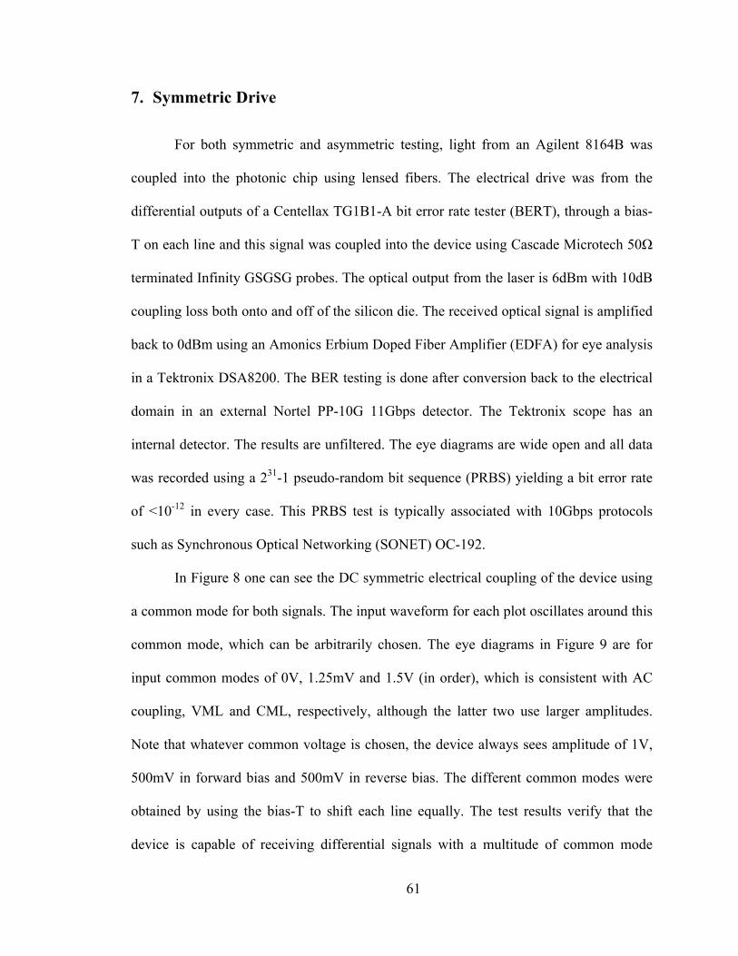
61
7. Symmetric Drive
For both symmetric and asymmetric testing, light from an Agilent 8164B was
coupled into the photonic chip using lensed fibers. The electrical drive was from the
differential outputs of a Centellax TG1B1-A bit error rate tester (BERT), through a bias-
T on each line and this signal was coupled into the device using Cascade Microtech 50Ω
terminated Infinity GSGSG probes. The optical output from the laser is 6dBm with 10dB
coupling loss both onto and off of the silicon die. The received optical signal is amplified
back to 0dBm using an Amonics Erbium Doped Fiber Amplifier (EDFA) for eye analysis
in a Tektronix DSA8200. The BER testing is done after conversion back to the electrical
domain in an external Nortel PP-10G 11Gbps detector. The Tektronix scope has an
internal detector. The results are unfiltered. The eye diagrams are wide open and all data
was recorded using a 231-1 pseudo-random bit sequence (PRBS) yielding a bit error rate
of <10-12 in every case. This PRBS test is typically associated with 10Gbps protocols
such as Synchronous Optical Networking (SONET) OC-192.
In Figure 8 one can see the DC symmetric electrical coupling of the device using
a common mode for both signals. The input waveform for each plot oscillates around this
common mode, which can be arbitrarily chosen. The eye diagrams in Figure 9 are for
input common modes of 0V, 1.25mV and 1.5V (in order), which is consistent with AC
coupling, VML and CML, respectively, although the latter two use larger amplitudes.
Note that whatever common voltage is chosen, the device always sees amplitude of 1V,
500mV in forward bias and 500mV in reverse bias. The different common modes were
obtained by using the bias-T to shift each line equally. The test results verify that the
device is capable of receiving differential signals with a multitude of common mode

62
voltages, rendering the same results and affording compatibility with different standards.
In the 500mV amplitude symmetric tests 7dB extinction is obtained.
To obtain compatibility with LVDS one can also demonstrate the performance
with a 400mV swing on each line for a total of 800mV into the device in Figure 10. The
common modes are the same. In the figures it is clear that the extinction degrades with
lower voltage, however 5dB is still achievable.
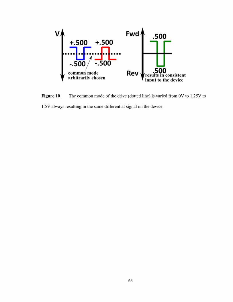
63
Figure 10 The common mode of the drive (dotted line) is varied from 0V to 1.25V to
1.5V always resulting in the same differential signal on the device.

64
Figure 11 Eye diagrams for common modes of 0mV, 1.25V and 1.5V at 500mV
show the same extinction level of 7dB verifying the flexibility of the device to DC couple
at arbitrary voltage levels.
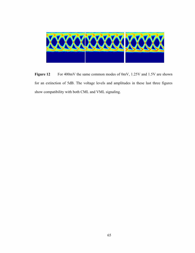
65
Figure 12 For 400mV the same common modes of 0mV, 1.25V and 1.5V are shown
for an extinction of 5dB. The voltage levels and amplitudes in these last three figures
show compatibility with both CML and VML signaling.
66
8. Asymmetric Drive
Figures 11-18 show the driving scheme and the resulting eye diagram for drive
amplitudes of 750mV down to 150mV using an asymmetric drive. This approach is not
readily transferable to commonly used differential signaling standards. However, it was
found that one could drive the modulators with 150mV signals to get 4dB extinction
using this technique although with 500mV signals the performance is comparable to the
symmetric case. The concept is to drive a modulator more into forward than reverse with
small enough amplitude so as not to go beyond diode turn on which introduces so many
free carriers in the depletion region that the electrical bandwidth is then limited by the
recombination lifetime. In this way, small voltages take advantage of the square root
function of depletion width which changes most efficiently just below diode turn on [19].
As in the symmetric case, the signal on the device is twice the amplitude because
differential signaling is used. So for the first figure, two differential 750mV signals result
in 1.5V on the device. By applying positive voltage to the cathode (red in the figures) the
signal is pushed into partial reverse bias as shown in green in Figure 11. This method of
biasing the cathode is used in each of the four reverse bias demonstrations. As the voltage
amplitude drops below 300mV it is possible to drive the modulator completely in forward
bias, yet below the diode turn on. Note that although the 300mV signal can achieve a 5dB
extinction as with the 400mV symmetric case, it is noisier. The noise is the result of more
free carriers being present in the sub-threshold forward bias domain. The extinction ratios
are 8dB for the 750mV signal, 7dB for 500mV, 5dB for 300mV and 4dB for 150mV.
67
Figure 13 750mV drive amplitude on both the P (blue) and N (red) silicon contacts
on device. The resulting 1.5V amplitude signal is shown in green to be slightly reversed
biased because of the 300mV negative DC bias offset driven in the N silicon through the
use of a bias-T.
68
Figure 14 The corresponding 10Gbps eye diagram shows 8dB extinction.

69
Figure 15 500mV drive amplitude on both the P (blue) and N (red) silicon contacts
on device. The resulting 1V amplitude signal is shown in green to be slightly forward
biased because of the 300mV positive DC bias offset driven in the N silicon through the
use of a bias-T. The slight forward bias is beneficial because the depletion region
expands according to the square root of the voltage applied.
70
Figure 16 The corresponding 10Gbps eye diagram shows 7dB extinction.
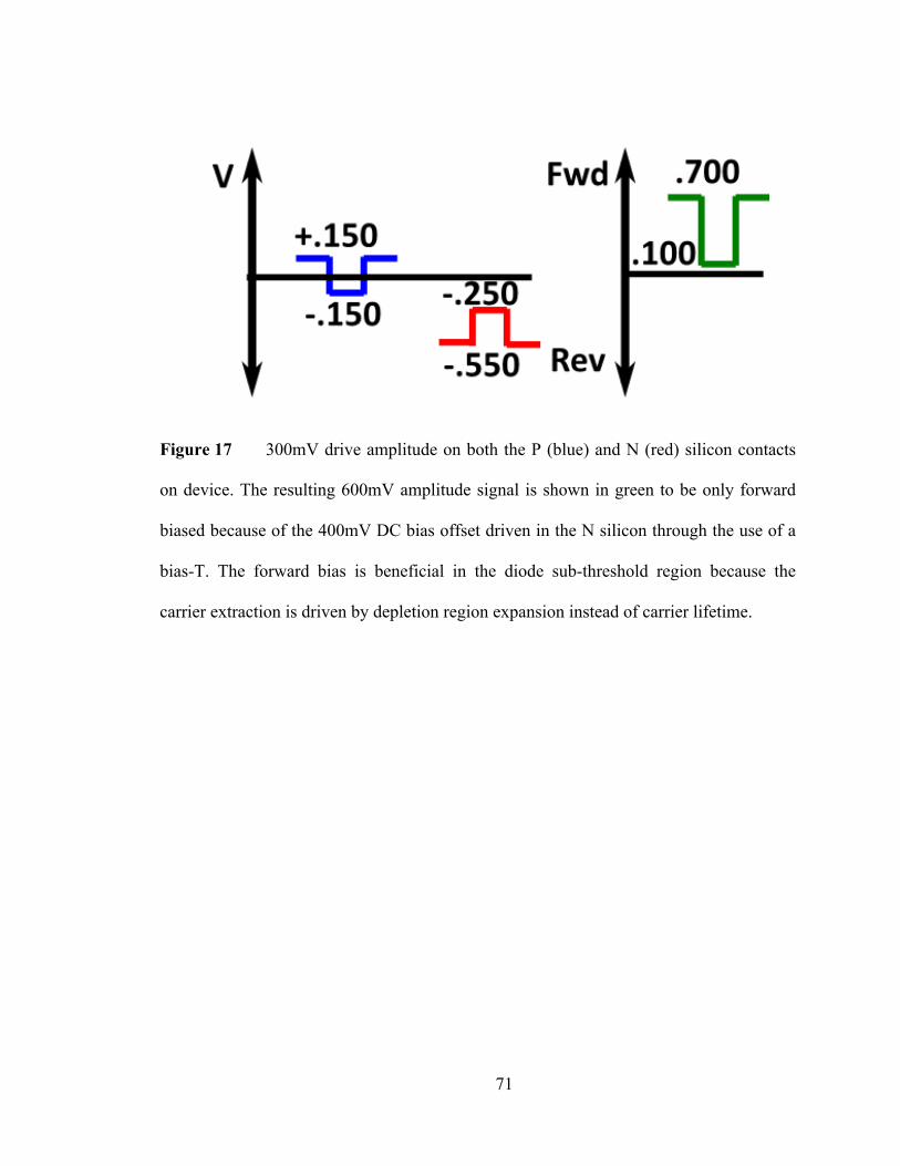
71
Figure 17 300mV drive amplitude on both the P (blue) and N (red) silicon contacts
on device. The resulting 600mV amplitude signal is shown in green to be only forward
biased because of the 400mV DC bias offset driven in the N silicon through the use of a
bias-T. The forward bias is beneficial in the diode sub-threshold region because the
carrier extraction is driven by depletion region expansion instead of carrier lifetime.
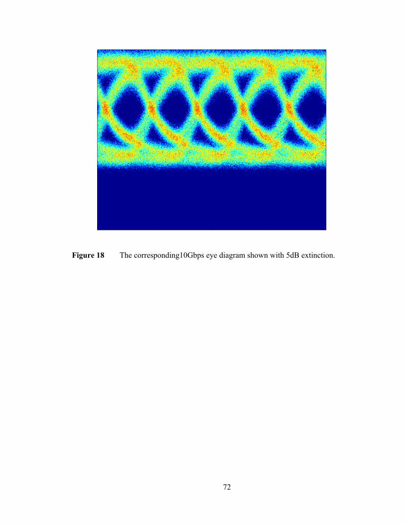
72
Figure 18 The corresponding10Gbps eye diagram shown with 5dB extinction.
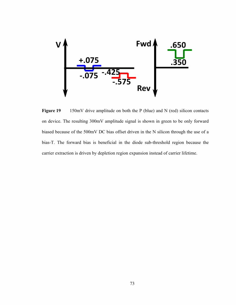
73
Figure 19 150mV drive amplitude on both the P (blue) and N (red) silicon contacts
on device. The resulting 300mV amplitude signal is shown in green to be only forward
biased because of the 500mV DC bias offset driven in the N silicon through the use of a
bias-T. The forward bias is beneficial in the diode sub-threshold region because the
carrier extraction is driven by depletion region expansion instead of carrier lifetime.
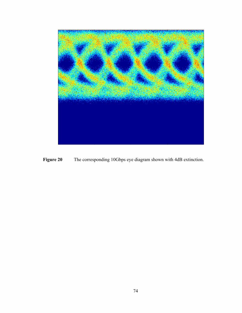
74
Figure 20 The corresponding 10Gbps eye diagram shown with 4dB extinction.
75
The above plots show the potential that is available if free level shifting of drivers
can be obtained. For example, to obtain the results in Figure 14 it would be necessary to
create a -200mV bias on the output drive of the transmitter chip. This may be desirable,
however it requires drivers without a common mode voltage. The enhanced noise in
forward bias could be reduced with mask filtering or band-pass filtering.
9. Energy per bit
The energy per bit is calculated using the full amplitude of the voltage on device.
The energy per bit has been measured using time domain reflectometry (TDR) in ½ volt
increments. Additionally an analytical estimation of capacitance was obtained using the
depletion approximation [18], which was supported by integrating the simulated charge
movement in DAVINCI software from Synopsys. In particular energy results are based
on integrating the voltage over time in the case of TDR measurement, calculating the
energy from E=CV2 in the analysis, and integrating the charge over time in the
simulations. In each case, four divides the final energy because the probability of
switching from 0 to 1 is only ¼ of the total switching space (00 01 10 11).
Finding good agreement among the different methods [9], the energy per bit
values in the symmetric case are found to be 3.2fJ/bit for 1V (500mV signal) and 2fJ/bit
for the 800mV (400mV signal).
In the case of the asymmetric drive the energies are approximately the same for
the 500mV amplitude. For the other cases 10.1 fJ/bit for 1.5V (750mV signal), 1.2fJ/bit
for 600mV (300mV signal) and 900aJ/bit for the 300mV (150mV signal) are found.
76
10. Summary
Differential signaling into silicon photonic resonators provides a promising
method of realizing both the low voltage CMOS and low power drivers envisioned for
enabling exascale computing. The symmetric drive capabilities demonstrated here are
compatible with typical low voltage differential signaling techniques in that they use the
same common mode voltages and voltage swings. Additionally, asymmetric coupling of
the modulators is shown to be a potential solution for even lower voltage applications.
Symmetrically driven, the modulator uses as low as 2fJ/bit with a signal amplitude of
400mV. Asymmetrically, 1.2fJ/bit can be obtained with 300mV of signal amplitude. In
both cases, the silicon modulators operate at 10Gbps with BER <10-12.

77
11. References
1. Xu, Q., Schmidt, B., Pradhan, S. and Lipson, M., Micrometre-scale silicon electro-optic modulator, Nature, Vol. 435, pp. 325-327, 19 May 2005.
2. S. Manipatruni, Q. Xu, B. Schmidt, J. Shakya, and M. Lipson, “High speed carrier injection 18 Gb/s silicon micro-ring electro-optic modulator,” in Proceedings of LEOS2007 (IEEE 2007), pp. 537–538.
3. Po Dong, Shirong Liao, Dazeng Feng, Hong Liang, Dawei Zheng, Roshanak Shafiiha, Cheng-Chih Kung, Wei Qian, Guoliang Li, Xuezhe Zheng, Ashok V. Krishnamoorthy, and Mehdi Asghari, "Low Vpp, ultralow-energy, compact, high-speed silicon electro-optic modulator," Opt. Express 17, 22484-22490 (2009) http://www.opticsinfobase.org/abstract.cfm?URI=oe-17-25-22484
4. G. Reed, F. Y. Gardes, G. Z. Mashanovich, Y., Hu, D. Thomson, G. Rasigade, D. Marris-Morini, and L. Vivien, "Recent Developments in Silicon Optical Modulators," in Integrated Photonics Research, Silicon and Nanophotonics, OSA Technical Digest (CD) (Optical Society of America, 2010), paper IWA1. http://www.opticsinfobase.org/abstract.cfm?URI=IPRSN-2010-IWA1
5. Watts, M.R.; Zortman, W.A.; Trotter, D.C.; Young, R.W.; Lentine, A.L.; , "Low-Voltage, Compact, Depletion-Mode, Silicon Mach–Zehnder Modulator," Selected Topics in Quantum Electronics, IEEE Journal of , vol.16, no.1, pp.159-164, Jan.-feb. 2010 doi: 10.1109/JSTQE.2009.2035059 URL: http://ieeexplore.ieee.org/stamp/stamp.jsp?tp=&arnumber=5395612&isnumber=5406274
6. Watts, M.R.; Trotter, D.C.; Young, R.W.; Lentine, A.L.; , "Ultralow power silicon microdisk modulators and switches," Group IV Photonics, 2008 5th IEEE International Conference on , vol., no., pp.4-6, 17-19 Sept. 2008 doi: 10.1109/GROUP4.2008.4638077 URL: http://ieeexplore.ieee.org/stamp/stamp.jsp?tp=&arnumber=4638077&isnumber=4638071
7. Zortman, William A.; Watts, Michael R.; Trotter, Douglas C.; Young, Ralph W.; Lentine, Anthony L.; , "Low-power high-speed silicon microdisk modulators," Lasers and Electro-Optics (CLEO) and Quantum Electronics and Laser Science Conference (QELS), 2010 Conference on , vol., no., pp.1-2, 16-21 May 2010
8. Po Dong, Shirong Liao, Hong Liang, Wei Qian, Xin Wang, Roshanak Shafiiha, Dazeng Feng, Guoliang Li, Xuezhe Zheng, Ashok V. Krishnamoorthy, and Mehdi Asghari, "High-speed and compact silicon modulator based on a racetrack resonator with a 1 V drive voltage," Opt. Lett. 35, 3246-3248 (2010) http://www.opticsinfobase.org/abstract.cfm?URI=ol-35-19-3246
9. Watts, M.R, Zortman, W.A., et al.; , unpublished, to be submitted to Optics Express
10. R. Soref, B. Bennett, “Electrooptical Effects in Silicon”, IEEE Journal of Quantum Electronics Vol QE-23 No. 1, 123-129 (1987)
11. J. M. Rabaey, A. Chandrakasan, B. Nikolic, Digital Integrated Circuits, Prentice Hall, New Jersey (2003)
78
12. Sasikanth Manipatruni, Kyle Preston, Long Chen, and Michal Lipson, "Ultra-low voltage, ultra-small mode volume silicon microring modulator," Opt. Express 18, 18235-18242 (2010) http://www.opticsinfobase.org/abstract.cfm?URI=oe-18-17-18235
13. Krishnamoorthy, A.V.; Ron Ho; Xuezhe Zheng; Schwetman, H.; Jon Lexau; Koka, P.; GuoLiang Li; Shubin, I.; Cunningham, J.E.; , "Computer Systems Based on Silicon Photonic Interconnects," Proceedings of the IEEE , vol.97, no.7, pp.1337-1361, July 2009 doi: 10.1109/JPROC.2009.2020712 URL: http://ieeexplore.ieee.org/stamp/stamp.jsp?tp=&arnumber=5071306&isnumber=5075744
14. Peter M. Kogge (editor), "ExaScale Computing Study: Technology Challenges in Achieving Exascale Systems," Univ. of Notre Dame, CSE Dept. Tech. Report TR-2008-13, Sept. 28, 2008
15. Berg, Y.; Mirmotahari, O.; Lomsdalen, J.G.; Aunet, S.; , "High Speed Ultra Low Voltage CMOS inverter," Symposium on VLSI, 2008. ISVLSI '08. IEEE Computer Society Annual , vol., no., pp.122-127, 7-9 April 2008 doi: 10.1109/ISVLSI.2008.23
16. Intel Quick Path Architecture http://www.intel.com/technology/quickpath/introduction.pdf January 2009
17. Byungsub Kim; Stojanovic, V.; , "A 4Gb/s/ch 356fJ/b 10mm equalized on-chip interconnect with nonlinear charge-injecting transmit filter and transimpedance receiver in 90nm CMOS," Solid-State Circuits Conference - Digest of Technical Papers, 2009. ISSCC 2009. IEEE International , vol., no., pp.66-67,67a, 8-12 Feb. 2009 doi: 10.1109/ISSCC.2009.4977310 URL: http://ieeexplore.ieee.org/stamp/stamp.jsp?tp=&arnumber=4977310&isnumber=4977283
18. Jae-sun Seo; Ron Ho; Lexau, J.; Dayringer, M.; Sylvester, D.; Blaauw, D.; , "High-bandwidth and low-energy on-chip signaling with adaptive pre-emphasis in 90nm CMOS," Solid-State Circuits Conference Digest of Technical Papers (ISSCC), 2010 IEEE International , vol., no., pp.182-183, 7-11 Feb. 2010 doi: 10.1109/ISSCC.2010.5433993 URL: http://ieeexplore.ieee.org/stamp/stamp.jsp?tp=&arnumber=5433993&isnumber=5433812
19. Neaman, Donald A., “Semiconductor Physics and Devices,” McGraw Hill, Boston (2003)
79
Chapter Three: Monolithic and Two-Dimensional
Integration of Silicon Photonic Microdisks with
Microelectronics
Many silicon photonic devices with high bandwidth and low power have been
demonstrated recently [1-7]. For the most part these are compatible with high volume
manufacturing in silicon through hybrid integration using chip bonding [8,9], backend
integration within a complementary metal oxide semiconductor (CMOS) process [10], or
otherwise monolithically in the front end of the process [11]. The intent is close
integration of optical communication devices with the silicon CMOS platform in order to
provide high bandwidth/low energy interconnect for future multiprocessors, high
performance computers and data centers [12,13].
Other groups have done demonstrations of integration of photonics with
electronics using silicon and other substrates [14,15]. This work demonstrates 2D
integration and monolithic integration of silicon photonics and electronics where the on
chip electronics drive the modulator. It is noteworthy that no change to the standard
80
CMOS process was required. This “drop-in” capability highlights the advantage of
silicon photonics over other optical interconnection technologies, such as vertical cavity
surface emitting lasers (VCSELS), for integration with existing high volume
manufacturing CMOS operations.
Two concepts are demonstrated, two-dimensional wire bonding and monolithic
integration. Two dimensional integration means that the discrete chips sit side by side as
opposed to 3D integration where the parts are stacked. The 2D demonstration uses a
Sandia designed and manufactured silicon photonic chip wire bonded to a standard IBM
90nm CMOS driver. The second approach is a monolithic integration of the same
photonic device with an inverter chain that drives the photonics. The two schemes are
useful for comparison and also demonstrate two potential uses for integrated photonics
and electronics.
81
1. The Discrete Photonic Device
The photonic device is fabricated in 250nm thick silicon on 3µm buried oxide
using a 0.35µm process on 6-inch silicon on insulator (SOI) wafers. This is the standard
process used on Sandia’s Microelectronics Development Lab (MDL), which is an active
manufacturing line that also runs application specific integrated circuit (ASIC) parts for
numerous terrestrial and space applications and as such the products are radiation
hardened (RADHARD). The photonic device that was integrated is shown in Figure 1
and has been described in [7]. The device is 3.5µm in diameter with 0.5µm tungsten filled
contacts connecting to a metal 2 interconnect which is 2µm above the surface of the
silicon. The contacts liners are titanium which are silicided (TiSi2) to 1020 doped P and N
ohmic contact regions. These regions are separated from each other by 100nm of filled
oxide trench in the monolithic application discussed below. There is a vertical PN
junction in the periphery doped to 1018 with N type dopants on the bottom and P type on
the top. The peripheral PN junction limits the junction capacitance resulting in higher
speed. The device is optically coupled to a 400nm wide bus waveguide across a 350nm
gap in the coupling region. There are 10µm of buried oxide covering the silicon and there
is 3µm of buried oxide underneath the silicon.
82
Figure 1 This three-dimensional representation of the 3.5 micron diameter disk
resonator is different from the device introduced in the last chapter. It is still
fabricated using 250nm thick silicon on 3µm buried oxide. There is 5µm
deposited oxide over the device and waveguide. The P-type ohmic contact is
approximately 100nm thick and the N-type is the full thickness of the silicon and
both ohmic contact regions are 2µm wide at the maximum. The integrated device
adds 100nm oxide strip to reduce capacitive coupling between the ohmic contacts.
83
The device DC performance in its discrete form is shown in Fig 2. The DC plot
shows ~10dB extinction and if the laser line is at the zero detuning point then 2dB
insertion loss is seen above and beyond the waveguide loss off resonance. When coupling
on/off chip there is 20dB loss when using lensed fibers. The Q is about 104. Fig 3 shows
that this device can achieve 7dB extinction using a 3.5V drive voltage at 10Gbps
although the other version of this device from chapter 1 with a smaller diode region [7]
achieves higher speed. The bit error rate is <10-12. The discrete performance is shown
here for comparison to the integrated devices. The energy consumed per bit is about
50fJ/bit at 3.5V if pad capacitance is not taken into account.
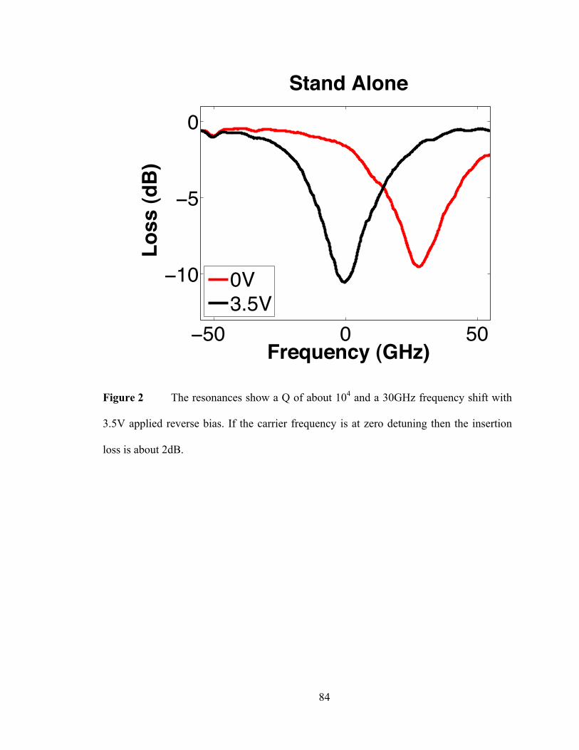
84
Figure 2 The resonances show a Q of about 104 and a 30GHz frequency shift with
3.5V applied reverse bias. If the carrier frequency is at zero detuning then the insertion
loss is about 2dB.
50 0 50
10
5
0
Frequency (GHz)
Los
s (d
B)
Stand Alone
0V3.5V

85
Figure 3 The discrete part 10Gbps eye diagram shows greater than 7dB extinction
using a 3.5V reverse bias.
Time (ps)
Tra
nsm
issi
on
Disk 3.5V Drive
125 250
1
0
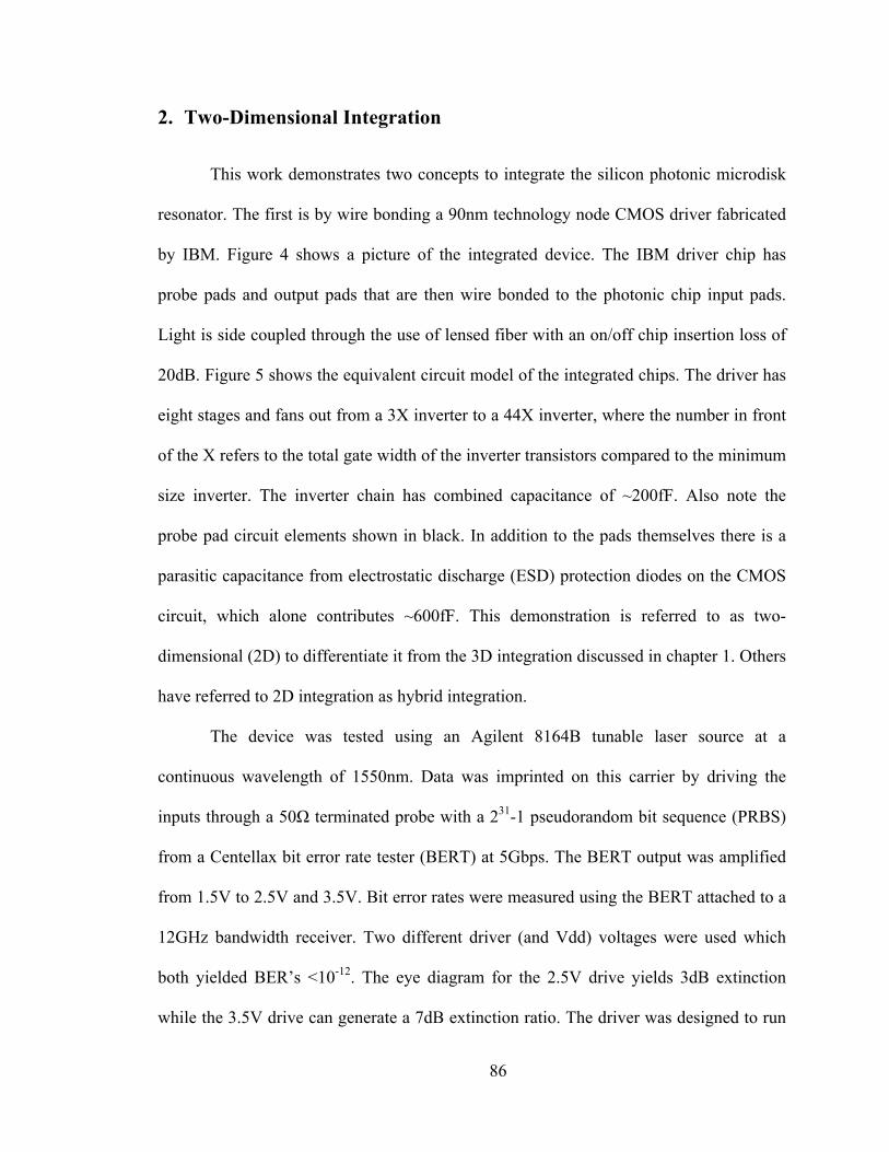
86
2. Two-Dimensional Integration
This work demonstrates two concepts to integrate the silicon photonic microdisk
resonator. The first is by wire bonding a 90nm technology node CMOS driver fabricated
by IBM. Figure 4 shows a picture of the integrated device. The IBM driver chip has
probe pads and output pads that are then wire bonded to the photonic chip input pads.
Light is side coupled through the use of lensed fiber with an on/off chip insertion loss of
20dB. Figure 5 shows the equivalent circuit model of the integrated chips. The driver has
eight stages and fans out from a 3X inverter to a 44X inverter, where the number in front
of the X refers to the total gate width of the inverter transistors compared to the minimum
size inverter. The inverter chain has combined capacitance of ~200fF. Also note the
probe pad circuit elements shown in black. In addition to the pads themselves there is a
parasitic capacitance from electrostatic discharge (ESD) protection diodes on the CMOS
circuit, which alone contributes ~600fF. This demonstration is referred to as two-
dimensional (2D) to differentiate it from the 3D integration discussed in chapter 1. Others
have referred to 2D integration as hybrid integration.
The device was tested using an Agilent 8164B tunable laser source at a
continuous wavelength of 1550nm. Data was imprinted on this carrier by driving the
inputs through a 50Ω terminated probe with a 231-1 pseudorandom bit sequence (PRBS)
from a Centellax bit error rate tester (BERT) at 5Gbps. The BERT output was amplified
from 1.5V to 2.5V and 3.5V. Bit error rates were measured using the BERT attached to a
12GHz bandwidth receiver. Two different driver (and Vdd) voltages were used which
both yielded BER’s <10-12. The eye diagram for the 2.5V drive yields 3dB extinction
while the 3.5V drive can generate a 7dB extinction ratio. The driver was designed to run

87
at 2.5V so the 3.5V data is the result of overdriving the part. The ESD protection at
~600fF coupled to the pad capacitance at ~30fF with a 50 ohm input limits the speed of
the system to about 5Gbps above which significant eye closure is seen. To calculate the
energy per bit of this integrated modulator-driver, the total power is calculated from the
voltage and current and then divided by the bit rate. For the 2.5V drive, the current is
3.2mA for a total power consumption of 8mW and energy per bit of 1.6pJ/bit. In the case
of the 3.5V drive voltage, a drive current of 3.2mA is measured, total power consumption
of 11.2mW and an energy consumption of 2.2pJ/bit. These results are summarized and
compared to the monolithic and discrete driver in the final section.
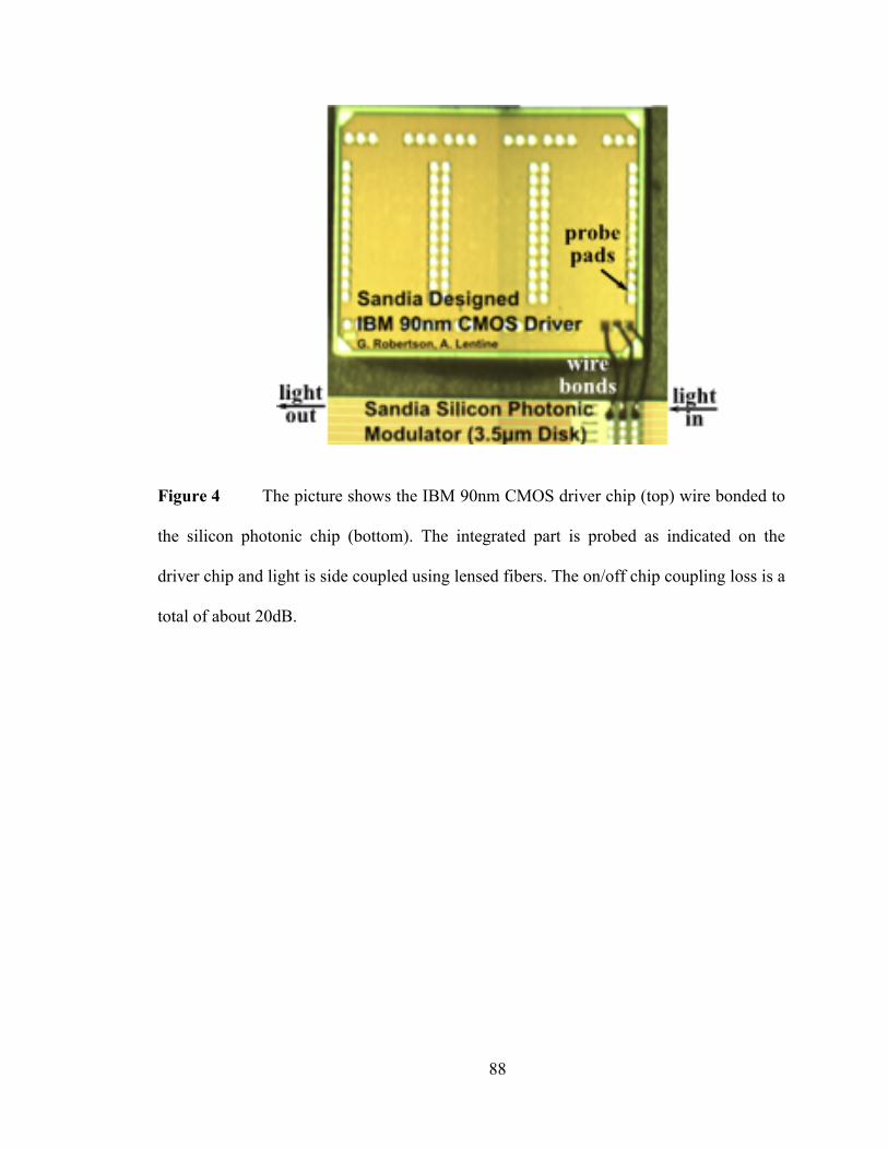
88
Figure 4 The picture shows the IBM 90nm CMOS driver chip (top) wire bonded to
the silicon photonic chip (bottom). The integrated part is probed as indicated on the
driver chip and light is side coupled using lensed fibers. The on/off chip coupling loss is a
total of about 20dB.
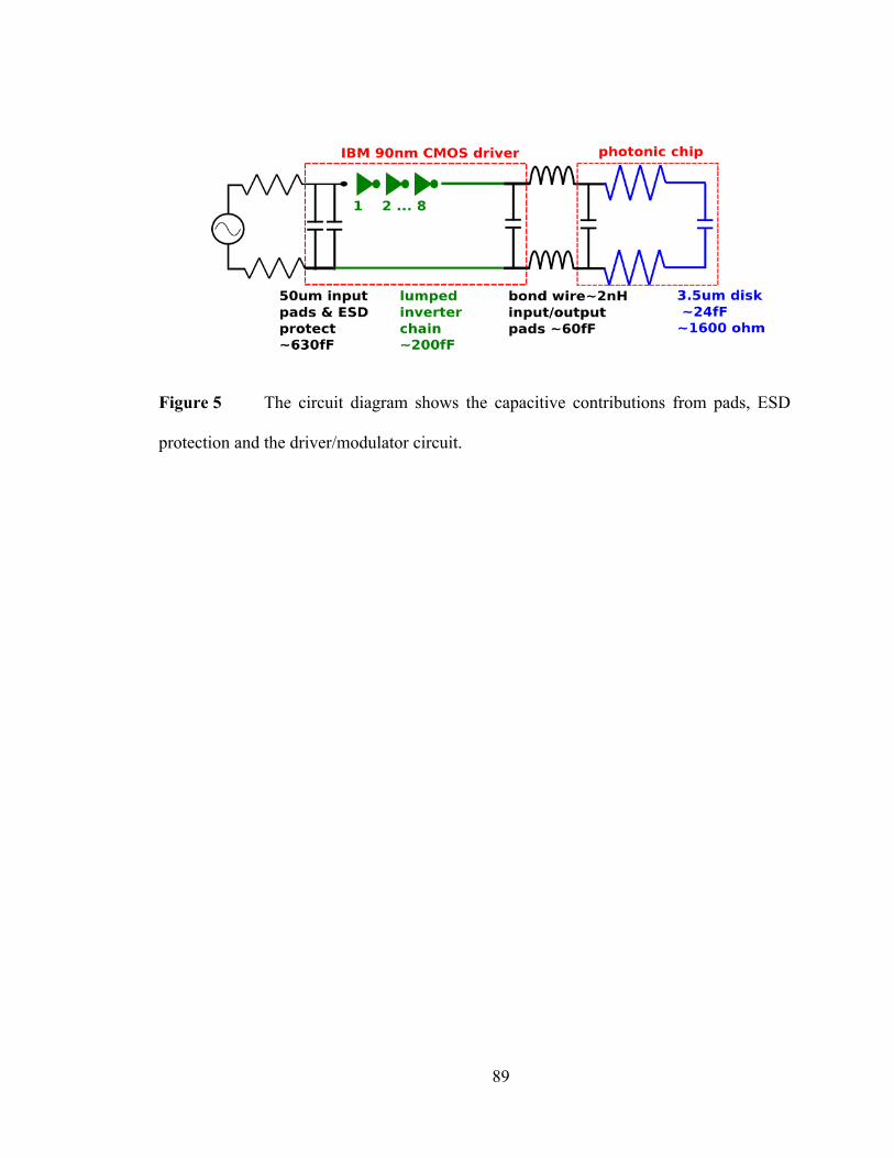
89
Figure 5 The circuit diagram shows the capacitive contributions from pads, ESD
protection and the driver/modulator circuit.
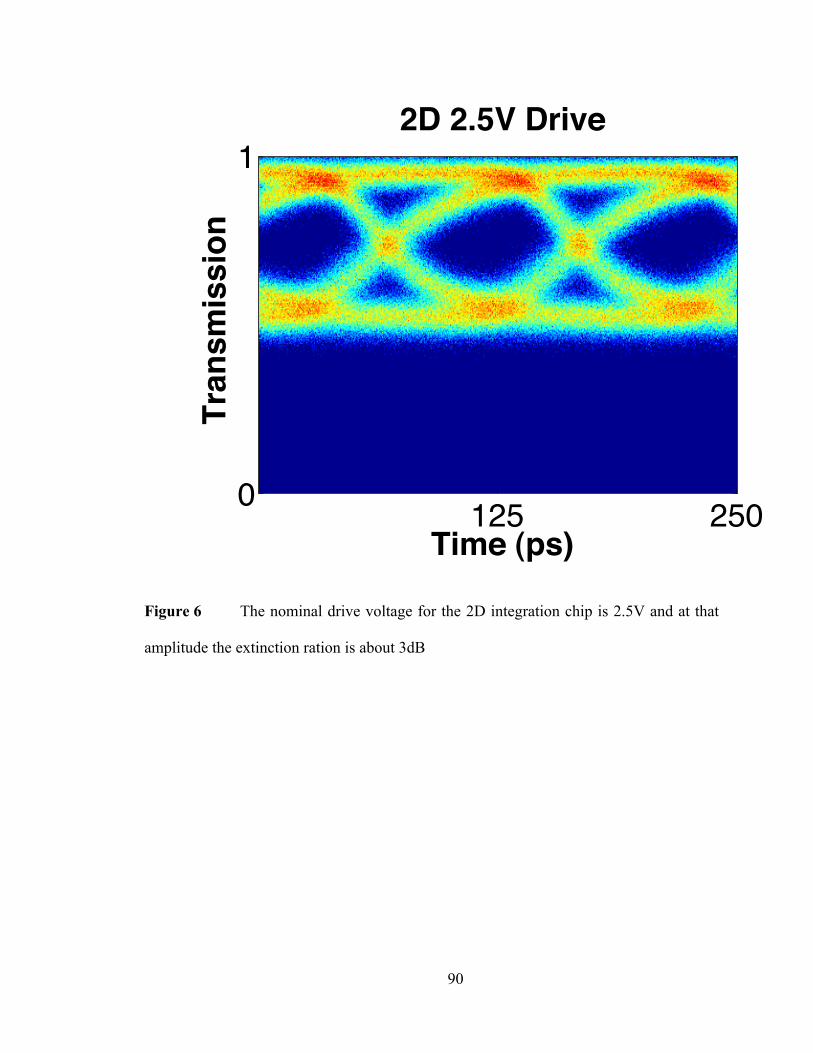
90
Figure 6 The nominal drive voltage for the 2D integration chip is 2.5V and at that
amplitude the extinction ration is about 3dB
Time (ps)
Tra
nsm
issi
on
2D 2.5V Drive
125 250
1
0
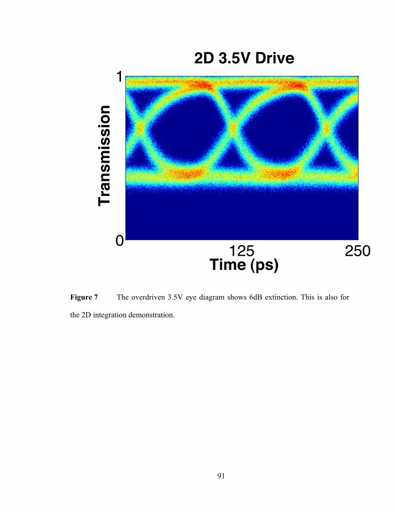
91
Figure 7 The overdriven 3.5V eye diagram shows 6dB extinction. This is also for
the 2D integration demonstration.
Time (ps)
Tra
nsm
issi
on
2D 3.5V Drive
125 250
1
0
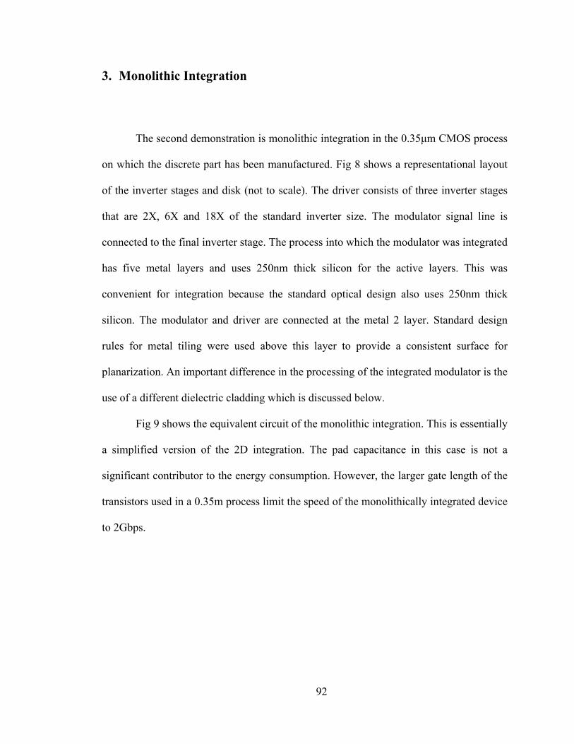
92
3. Monolithic Integration
The second demonstration is monolithic integration in the 0.35µm CMOS process
on which the discrete part has been manufactured. Fig 8 shows a representational layout
of the inverter stages and disk (not to scale). The driver consists of three inverter stages
that are 2X, 6X and 18X of the standard inverter size. The modulator signal line is
connected to the final inverter stage. The process into which the modulator was integrated
has five metal layers and uses 250nm thick silicon for the active layers. This was
convenient for integration because the standard optical design also uses 250nm thick
silicon. The modulator and driver are connected at the metal 2 layer. Standard design
rules for metal tiling were used above this layer to provide a consistent surface for
planarization. An important difference in the processing of the integrated modulator is the
use of a different dielectric cladding which is discussed below.
Fig 9 shows the equivalent circuit of the monolithic integration. This is essentially
a simplified version of the 2D integration. The pad capacitance in this case is not a
significant contributor to the energy consumption. However, the larger gate length of the
transistors used in a 0.35m process limit the speed of the monolithically integrated device
to 2Gbps.
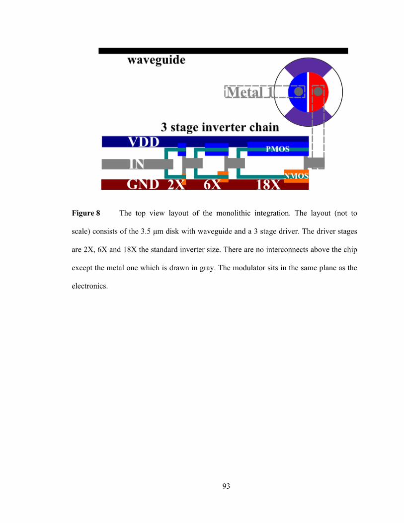
93
Figure 8 The top view layout of the monolithic integration. The layout (not to
scale) consists of the 3.5 µm disk with waveguide and a 3 stage driver. The driver stages
are 2X, 6X and 18X the standard inverter size. There are no interconnects above the chip
except the metal one which is drawn in gray. The modulator sits in the same plane as the
electronics.

94
Figure 9 The equivalent circuit of the monolithic optoelectronic driver and
modulator chip is a simplified version of the 2D integration. Not only is the contact pad
capacitance for bonding eliminated, but also the entire function fits within a few hundred
microns.
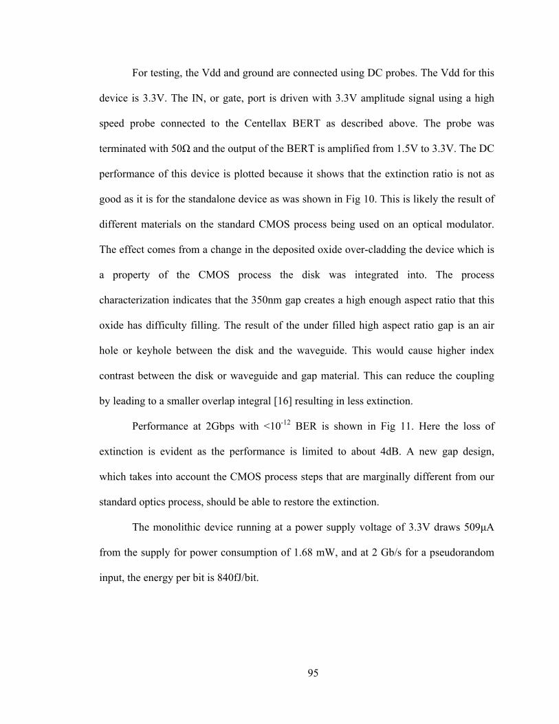
95
For testing, the Vdd and ground are connected using DC probes. The Vdd for this
device is 3.3V. The IN, or gate, port is driven with 3.3V amplitude signal using a high
speed probe connected to the Centellax BERT as described above. The probe was
terminated with 50Ω and the output of the BERT is amplified from 1.5V to 3.3V. The DC
performance of this device is plotted because it shows that the extinction ratio is not as
good as it is for the standalone device as was shown in Fig 10. This is likely the result of
different materials on the standard CMOS process being used on an optical modulator.
The effect comes from a change in the deposited oxide over-cladding the device which is
a property of the CMOS process the disk was integrated into. The process
characterization indicates that the 350nm gap creates a high enough aspect ratio that this
oxide has difficulty filling. The result of the under filled high aspect ratio gap is an air
hole or keyhole between the disk and the waveguide. This would cause higher index
contrast between the disk or waveguide and gap material. This can reduce the coupling
by leading to a smaller overlap integral [16] resulting in less extinction.
Performance at 2Gbps with <10-12 BER is shown in Fig 11. Here the loss of
extinction is evident as the performance is limited to about 4dB. A new gap design,
which takes into account the CMOS process steps that are marginally different from our
standard optics process, should be able to restore the extinction.
The monolithic device running at a power supply voltage of 3.3V draws 509µA
from the supply for power consumption of 1.68 mW, and at 2 Gb/s for a pseudorandom
input, the energy per bit is 840fJ/bit.
96
Figure 10 The DC performance of the integrated part. DC resonances are plotted and
show that the extinction ratio has been degraded. One of the reasons for this is an air gap
the oxide between the disk and waveguide.
50 0 50
10
5
0
Frequency (GHz)
Los
s (d
B)
Monolithic
3.3V0V
97
Figure 11 The bandwidth is limited by the performance of the 0.35µm technology
used for fabrication. A clear eye with about 4dB extinction is shown at 2Gbps.
Time (ps)
Tra
nsm
issi
on
Monolithic 2Gb/s
250 500 750 1000
1
0.4

98
4. Discussion
Table 1 gives a summary of the power and energy consumption of the discrete
part and integrated parts from this demonstration. This table includes the effect of the
ESD structures. The monolithic integration consumes less than ~840fJ/bit, which is half
of what the 2D integration consumes even though in one case the 2D device is using less
voltage. However, the greater energy consumption is almost exclusively due to the large
ESD diodes in the 2D device. This can be more easily identified in the detailed energy
histogram analysis of Figure 12, which pulls the ESD contribution out. Should the ESD
diodes be eliminated, both integrations can achieve less than 1pJ/bit. The optical
modulator used in these integrations has been shown to consume energy as low as 3fJ/bit
and operate with a single volt [7]. The current required for this level of switching is about
3mA at its peak meaning much smaller drivers with a single stage could drive the
devices. A single 3X inverter, for example in the 0.35µm process, would add less than
20fF which at 1V would result in total drive energies well below 50fJ/bit.
Demonstrated are two possible integrations of a low power silicon photonic
modulator with CMOS electronics. The monolithic integration shows the ready
integration that silicon photonics provides into standard CMOS manufacturing. Although
our process is based on thicker silicon than that typically used today on advanced
processors, the application to a photonic transmitter chip with integrated drivers is
apparent. The monolithic integration shows 840fJ/bit modulation energy while the 2D
integration at similar voltages is comparable to that. However, these drivers provide
much more current than is needed for the smallest modulators available today. With
smaller drivers more compatible with the current needed to run a small modulator the

99
energy per bit of monolithically integrated CMOS photonics and electronics can be
pushed much lower. There is no reason why a driver could not be scaled to result in the
energy/bit performance seen in Chapter 2. One to three femto-joule per bit operation
should be possible.
100
Table 1 The total energy consumption and bandwidth is summarized for each part,
discrete, monolithic and 2D integrated. These calculations include the ESD protection.
Device Power Energy BW
Discrete Disk 1V 32uW 3.2fJ/bit 10Gbps
Discrete Disk 3.5V 200uW ~50fJ/bit
(w/o pads)
10Gbps
Monolithic 3.3V 1.68mW 840fJ/bit 2Gbps
2D 2.5V 8mW 1.6pJ/bit 5Gbps
2D 3.5V 11.2mW 2.2pJ/bit 5Gbps
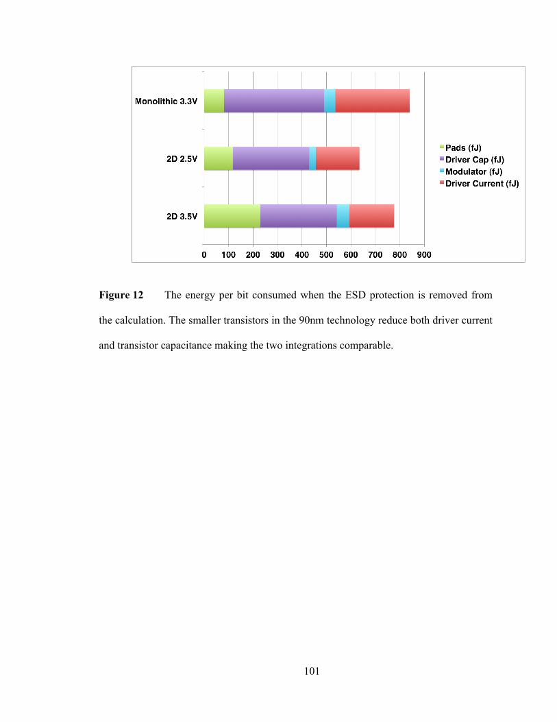
101
Figure 12 The energy per bit consumed when the ESD protection is removed from
the calculation. The smaller transistors in the 90nm technology reduce both driver current
and transistor capacitance making the two integrations comparable.

102
5. References
1. Xu, Q., Schmidt, B., Pradhan, S. and Lipson, M., Micrometre-scale silicon electro-optic modulator, Nature, Vol. 435, pp. 325-327, 19 May 2005.
2. S. Manipatruni, Q. Xu, B. Schmidt, J. Shakya, and M. Lipson, “High speed carrier injection 18 Gb/s silicon micro-ring electro-optic modulator,” in Proceedings of LEOS2007 (IEEE 2007), pp. 537–538.
3. Po Dong, Shirong Liao, Dazeng Feng, Hong Liang, Dawei Zheng, Roshanak Shafiiha, Cheng-Chih Kung, Wei Qian, Guoliang Li, Xuezhe Zheng, Ashok V. Krishnamoorthy, and Mehdi Asghari, "Low Vpp, ultralow-energy, compact, high-speed silicon electro-optic modulator," Opt. Express 17, 22484-22490 (2009) http://www.opticsinfobase.org/abstract.cfm?URI=oe-17-25-22484
4. G. Reed, F. Y. Gardes, G. Z. Mashanovich, Y. , Hu, D. Thomson, G. Rasigade, D. Marris-Morini, and L. Vivien, "Recent Developments in Silicon Optical Modulators," in Integrated Photonics Research, Silicon and Nanophotonics, OSA Technical Digest (CD) (Optical Society of America, 2010), paper IWA1. http://www.opticsinfobase.org/abstract.cfm?URI=IPRSN-2010-IWA1
5. Watts, M.R.; Zortman, W.A.; Trotter, D.C.; Young, R.W.; Lentine, A.L.; , "Low-Voltage, Compact, Depletion-Mode, Silicon Mach–Zehnder Modulator," Selected Topics in Quantum Electronics, IEEE Journal of , vol.16, no.1, pp.159-164, Jan.-feb. 2010 doi: 10.1109/JSTQE.2009.2035059 URL: http://ieeexplore.ieee.org/stamp/stamp.jsp?tp=&arnumber=5395612&isnumber=5406274
6. Watts, M.R.; Trotter, D.C.; Young, R.W.; Lentine, A.L.; , "Ultralow power silicon microdisk modulators and switches," Group IV Photonics, 2008 5th IEEE International Conference on , vol., no., pp.4-6, 17-19 Sept. 2008 doi: 10.1109/GROUP4.2008.4638077 URL: http://ieeexplore.ieee.org/stamp/stamp.jsp?tp=&arnumber=4638077&isnumber=4638071
7. Zortman, William A.; Watts, Michael R.; Trotter, Douglas C.; Young, Ralph W.; Lentine, Anthony L.; , "Low-power high-speed silicon microdisk modulators," Lasers and Electro-Optics (CLEO) and Quantum Electronics and Laser Science Conference (QELS), 2010 Conference on , vol., no., pp.1-2, 16-21 May 2010 URL: http://ieeexplore.ieee.org/stamp/stamp.jsp?tp=&arnumber=5500977&isnumber=5499482
8. Xuezhe Zheng, Jon Lexau, Ying Luo, Hiren Thacker, Thierry Pinguet, Attila Mekis, Guoliang Li, Jing Shi, Philip Amberg, Nathaniel Pinckney, Kannan Raj, Ron Ho, John E. Cunningham, and Ashok V. Krishnamoorthy, "Ultra-low-energy all-CMOS modulator integrated with driver," Opt. Express 18, 3059-3070 (2010) http://www.opticsinfobase.org/abstract.cfm?URI=oe-18-3-3059
9. Xuezhe Zheng, Frankie Liu, Dinesh Patil, Hiren Thacker, Ying Luo, Thierry Pinguet, Attila Mekis, Jin Yao, Guoliang Li, Jing Shi, Kannan Raj, Jon Lexau, Elad Alon, Ron Ho, John E. Cunningham, and Ashok V. Krishnamoorthy, "A sub-picojoule-per-bit CMOS photonic receiver for densely integrated systems," Opt. Express 18, 204-211 (2010) http://www.opticsinfobase.org/abstract.cfm?URI=oe-18-1-204
103
10. Kyle Preston, Bradley Schmidt, and Michal Lipson, "Polysilicon photonic resonators for large-scale 3D integration of optical networks," Opt. Express 15, 17283-17290 (2007) http://www.opticsinfobase.org/abstract.cfm?URI=oe-15-25-17283
11. Orcutt, J.S.; Khilo, A.; Popovic, M.A.; Holzwarth, C.W.; Moss, B.; Hanqing Li; Dahlem, M.S.; Bonifield, T.D.; Kartner, F.X.; Ippen, E.P.; Hoyt, J.L.; Ram, R.J.; Stojanovic, V.; , "Demonstration of an electronic photonic integrated circuit in a commercial scaled bulk CMOS process," Lasers and Electro-Optics, 2008 and 2008 Conference on Quantum Electronics and Laser Science. CLEO/QELS 2008. Conference on , vol., no., pp.1-2, 4-9 May 2008 URL: http://ieeexplore.ieee.org/stamp/stamp.jsp?tp=&arnumber=4571838&isnumber=4571172
12. Miller, D.; , "Device Requirements for Optical Interconnects to Silicon Chips," Proceedings of the IEEE , vol.97, no.7, pp.1166-1185, July 2009 doi: 10.1109/JPROC.2009.2014298 URL: http://ieeexplore.ieee.org/stamp/stamp.jsp?tp=&arnumber=5071309&isnumber=5075744
13. A. V. Krishnamoorthy, R. Ho, X. Zheng, H. Schwetman, J. Lexau, P. Koka, G. Li, I. Shubin, and J. E. Cunningham, “Computer systems based on silicon photonic interconnects,” Proc. IEEE 97, 1337–1361 (2009).
14. Ho, R.; Jon Lexau; Liu, F.; Patil, D.; Hopkins, R.; Alon, E.; Pinckney, N.; Amberg, P.; Xuezhe Zheng; Cunningham, J.E.; Krishnamoorthy, A.V.; , "Circuits for silicon photonics on a “macrochip”," Solid-State Circuits Conference, 2009. A-SSCC 2009. IEEE Asian , vol., no., pp.17-20, 16-18 Nov. 2009 doi: 10.1109/ASSCC.2009.5357232 URL: http://ieeexplore.ieee.org/stamp/stamp.jsp?tp=&arnumber=5357232&isnumber=5357143
15. Hsu-Hao Chang; Ying-hao Kuo; Hui-Wen Chen; Jones, R.; Barkai, A.; Paniccia, M.J.; Bowers, J.E.; , "Integrated triplexer on hybrid silicon platform," Optical Fiber Communication (OFC), collocated National Fiber Optic Engineers Conference, 2010 Conference on (OFC/NFOEC) , vol., no., pp.1-3, 21-25 March 2010 URL: http://ieeexplore.ieee.org/stamp/stamp.jsp?tp=&arnumber=5465392&isnumber=5465158
16. Haus, Hermann, “Waves and Fields in Optoelectronics”, Prentice Hall New Jersey 1984
104
Chapter Four: Silicon Photonics Manufacturing
1. Introduction
Future high-density chip-to-chip and high performance computing (HPC)
interconnect power consumption and off chip bandwidth requirements will be extremely
challenging or impossible to meet using electrical interconnects [1,2]. In [1] an energy/bit
target of 97fJ/bit (970µW at 10Gbps) is given for the off chip transmitter in a 22nm node
chip which is expected to be available in 2015. Recent demonstrations of silicon photonic
technology have shown that wavelength division multiplexed (WDM), low energy, high
bandwidth interconnect schemes are compatible with existing silicon high volume
manufacturing (HVM) techniques in microelectronics even if high volume integration is
still in its nascent stage [3-5]. Technologies have begun to emerge that embark on the
next step in integrating these discrete devices into systems [6-9].
With large-scale integration, devices will be repeated across wafers, lots, and
process runs to build systems. The uniformity of these devices is critical since high yield
is essential to continue the historic achievement of low cost in silicon parts during the age
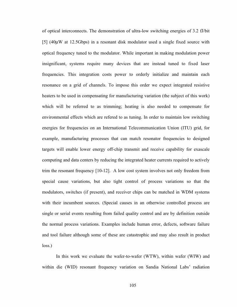
105
of optical interconnects. The demonstration of ultra-low switching energies of 3.2 fJ/bit
[5] (40µW at 12.5Gbps) in a resonant disk modulator used a single fixed source with
optical frequency tuned to the modulator. While important in making modulation power
insignificant, systems require many devices that are instead tuned to fixed laser
frequencies. This integration costs power to orderly initialize and maintain each
resonance on a grid of channels. To impose this order we expect integrated resistive
heaters to be used in compensating for manufacturing variation (the subject of this work)
which will be referred to as trimming; heating is also needed to compensate for
environmental effects which are refered to as tuning. In order to maintain low switching
energies for frequencies on an International Telecommunication Union (ITU) grid, for
example, manufacturing processes that can match resonator frequencies to designed
targets will enable lower energy off-chip transmit and receive capability for exascale
computing and data centers by reducing the integrated heater currents required to actively
trim the resonant frequency [10-12]. A low cost system involves not only freedom from
special cause variations, but also tight control of process variations so that the
modulators, switches (if present), and receiver chips can be matched in WDM systems
with their incumbent sources. (Special causes in an otherwise controlled process are
single or serial events resulting from failed quality control and are by definition outside
the normal process variations. Examples include human error, defects, software failure
and tool failure although some of these are catastrophic and may also result in product
loss.)
In this work we evaluate the wafer-to-wafer (WTW), within wafer (WIW) and
within die (WID) resonant frequency variation on Sandia National Labs’ radiation
106
hardened six inch Silicon on Insulator (SOI) 0.35µm process using 248nm lithography.
Then a new technique is used to extract the contributors to the variation and use this
information along with careful assumptions about future interconnect architecture and
current HVM capabilities to make estimates of the total power consumption, including
resonant frequency trimming and tuning, for future chip-to-chip silicon photonic links.
2. Resonant frequency variation across wafers
A previous report on Sandia’s process can be found in [13]. In the current work
the within die WID variation is also measured. Additionally, results are now presented
comparing metalized and non-metalized wafers from two fabrication facility (fab) runs so
that we can begin to see if metallization has an impact on resonant frequency variation
(e.g. due to strain, evanescent coupling, etc.).
Each wafer in this study had five nominally identical microdisk resonators
fabricated on adjacent waveguides with a 75µm separation between each waveguide for a
total of five devices across 300µm. The wafers used in this study are labeled W1 and W2;
W1 is metalized and contains fully contacted and doped resonators while W2 is silicon
only (does not have contacts or doped regions) and both have 5000Å of deposited oxide
above the silicon waveguides. This breadth of data gives us the ability to collect statistics
on the WID variation and begin to understand the impact of processing beyond the initial
etch to the silicon lattice (sometimes called the silicon cut). Additionally, data from [13]
is included as W0, which is from a different process run.
The resonator is a 6 micron diameter microdisk with a waveguide to disk
separation of 320nm fabricated on 240nm SOI over 3µm buried oxide using the same
process as described in [14]. Microdisks are chosen because their resonant frequencies
107
depend only on thickness and diameter, enabling dimensional variations to be easily
extracted from the results; furthermore the large free spectral range offered by these small
disks separates the resonances sufficiently to avoid confusion when determining the
resonant shift between devices. Resonators on all three wafers were measured along the
vertical axis of the wafer from the top down to the wafer flat (sometimes called the
notch). W1 and W2 had eight die with five identical disks on each die (a total of 40 data
points on each wafer). A schematic of the location of each measurement on the wafer is
shown in Figure 1. W0 had 12 die along the vertical axis and only one device per die (a
total of 12 data points).
Each device was measured using an Agilent 8164B swept laser source with
125MHz (1pm) frequency resolution. Light was coupled on chip using lensed fibers with
an on/off chip insertion loss of ~20dB. The chips were temperature controlled at 27OC to
within 0.01OC. Measured resonant frequency variation for 30 measurements on the same
disk had a three standard deviation (3σ) value of +/-250MHz, which is taken as the
resolution of our measurement.
108
Figure 1 The layout of the devices that were measured from Wafer 1 and Wafer 2.
Wafer 0 only had one device per chip, but followed the same measurement
scheme from top to notch.
109
In this chapter we only consider variations from the mean and not the variation
from the designed resonant frequency because it is assumed that a designer using a well
characterized, albeit variable process, will skew mask designs to compensate. Figure 2
shows a plot of the TE and TM resonant frequencies from top to bottom along the vertical
line of all three wafers. Each W1 and W2 data point is the mean of the five resonators in
that die. The TE frequency range is seen to be about 1THz and the TM varies by nearly
2.5THz. We are most interested in the TE modes because the modulators were designed
for that polarization, however the TM resonance will be important for Section 3 when the
dimensional deviations are extracted. Both wafers show that WIW variation is significant
when matching chips within a single wafer. The wider TM frequency range will be
discussed in detail in Section 3. Additionally, the trend from lower frequencies to higher
across all wafers will be shown in Section 3 to be the result of thickness variation, likely
driven by non-uniform planarization that is inherent in the SOI manufacturing process.
Table 1 is a summary of the wafer level data collected for the three wafers and it
shows significant WTW and WIW variation that cannot be attributed to metallization.
Comparison between wafers shows that there can be >1 THz of variation WTW. W0,
which was metalized has a lower standard deviation than W2 (silicon only) and
additionally W2 and W0 are closer in mean frequency than W0 and W1, the two metal
wafers. The outlier chip from the top of W2 was filtered out of the data and the result of
this filtering is shown in parentheses in Table 1. With this point removed the standard

110
Figure 2 The frequency deviation from the wafer mean by distance from wafer
center. All three wafers showed frequency increasing from top to notch and W1 had a
statistical outlier chip at the top of the wafer.
6 4 2 0 2 4 6
1000
500
0
500
1000
1500
2000
Distance from Center (cm) (top to bottom)
f f
rom
Waf
er M
ean
(GH
z)
Frequency Deviation by Wafer Location
W1 TEW1 TMW2 TEW2 TMW0 TEW0 TM
111
deviation falls below the silicon only wafer. The summary in Table 1 shows that while
there is significant WTW variation, conclusions about metallization cannot be drawn
from a single un-metalized wafer.
When examining the variation WIW and WTW it is instructive to keep in mind
the volumes at which chips are manufactured. In microelectronics even an 8 inch HVM
memory facility can achieve output levels of 10,000 wafers per week with thousands of
dice on each wafer for a total output of millions of dice weekly; this is compounded by
the fact that most manufacturers run several facilities on the same process. It is therefore
important to ask if the same level of output will be achieved in silicon photonics because
with a large volume of dice it should be possible to match chips from different wafers and
lots to minimize the chip- to-chip variation; this idea will be explored further below.
Therefore, quantifying the WID variation is of interest. To understand the WID variation
it is first necessary to quantify what is driving the variation. This is done using a new
technique in the next section.
112
Table 1 The mean, standard deviation and median for the resonant wavelengths of the
devices across the three wafers. Data with the first chip filtered out of W1 is shown in
parenthesis
W0 [metal] From [13]
W1 [metal] (filtered)
W2 [Si only]
|W1-W2|
TE Mean (THz)
192.0 191.0 (191.2) 192.2 1.117
TE Std Dev (GHz)
285 556 (357) 430 126
TE Median (THz)
192.0 191.0 (191.0) 192.0 0.966
TM Mean (THz)
195.8 194.1 (194.5) 194.8 0.666
TM Std Dev (GHz)
741 1,194 (749) 957 237
TM Median (THz)
195.7 194.2 (194.2) 194.4 0.215
113
3. Demonstration of a new technique to extract dimensional variation
In a microdisk, frequency variation is the result of thickness and diameter
variations alone. Using a cylindrical modesolver [15] the modes were calculated (Fig 3
and 4) at different diameters and thicknesses to determine their sensitivity to both
dimensional variations. In general, the modal frequencies depend on both the mode
number and design dimensions and are most accurately represented as a function with the
aforementioned dependencies. This function can be expanded in a Taylor series and in
cases where the dimensions do not vary substantially from the design dimensions, higher
order terms may be dropped. Such is the case in this analysis. The calculated first order
sensitivities are presented in Table 2 about a resonant wavelength of λ = 1550nm.
The sensitivity of both the TE and TM modes to layer thickness variations is
much larger than to diameter variations. This is particularly true in the case of the TM
mode for which the sensitivity to thickness variations is nearly ten-fold higher than it is to
diameter variations. It is for this reason that the TM modes suffer from much greater
frequency variation across each wafer (Figure 2).
To definitively isolate the cause of the resonant frequency variation, we can write
the pair of equations describing the TE and TM resonant frequencies in matrix form.
Since this matrix represents a linear invertible system of two equations and two
unknowns, it provides for a unique solution. The measured frequency variations are on
the right side, and the mode solver prediction from Table 2 in the 2x2 matrix on the left.
The two unknowns, ΔT and ΔD are the disk-to-disk thickness and diameter changes,
respectively, which are in the vector that completes the system:
114
dfdT TE
dfdD TE
dfdT TM
dfdD TM
!
"
#####
$
%
&&&&&
' (T(D
!
"#
$
%& =
(fTE(fTM
!
"##
$
%&&
(1)
By inserting the data from W1 and W2 from Figure 2 into the right side of
equation (1) the dimensional variations can be extracted.
The results of the calculation are plotted in Figure 5, which shows the
dimensional variations that are driving the frequency variations from Figure 2 W0 was
eliminated for clarity. W1 has a larger diameter variation although within 3cm of the
center of the wafer the difference is not significant from W2. Figure 6 shows the
reconstructed TE frequency shift for W1 as the sum of the thickness and diameter
variations. Diameter deviations on W1, although larger and contributing 250GHz of
variation are less significant when considering the edge thickness contribution which is
2THz as depicted in Figure 6. Eliminating the outlier reduces that variation to 1THz.
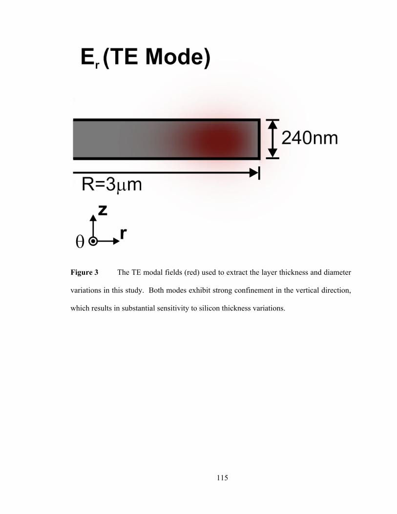
115
Figure 3 The TE modal fields (red) used to extract the layer thickness and diameter
variations in this study. Both modes exhibit strong confinement in the vertical direction,
which results in substantial sensitivity to silicon thickness variations.
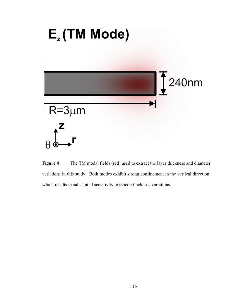
116
Figure 4 The TM modal fields (red) used to extract the layer thickness and diameter
variations in this study. Both modes exhibit strong confinement in the vertical direction,
which results in substantial sensitivity to silicon thickness variations.

117
Table 2 The predicted frequency deviation is given for a dimensional deviation in both
thickness and diameter. Thickness is the dominant driver of frequency variation although
diameter is more significant in the pertinent TE modes.
Polarization Thickness Diameter
TE -140GHz/nm -52GHz/nm
TM -330GHz/nm -36GHz/nm

118
4. Within die variation
The data from Section 2 can be averaged for each chip (a total of 8 averages) on
W1 and W2. Then each resonator on each die can be compared to the die average to
calculate the WID variation using all forty measured data points (5 points per die). This
provides forty data points per wafer and through the use of Equation (1) we can then
calculate an average within die variation, which is plotted in Figure 7. Thickness
variations within die are limited to +/-0.1nm, which is expected over such a small
distance. Resonator diameter variations are unexpectedly severe with close to +/-0.35nm
variation on average across a 300µm distance and both wafers follow a similar trend from
device to device for diameter variation.
The repeatability of the WID trend on two wafers shown in Figure 7 is
hypothesized to be caused by a mask error (a special cause) as consistent printing of the
same feature sizes would explain the error repeatability across sixteen dice on two
wafers. An analysis of variance (anova) test of the WID variation of the mean for each
disk shows that the diameters for each disk do not come from the same distribution with a
probability of this being the case being well below 1% (P-value<0.01) suggesting a
special cause is driving the variation as opposed to the normal process variation. (Anova
is a statistical tool for comparing more than two distributions using methods similar to the
two sample t-test which compares two distributions. Both tests determine if the difference
in the mean of the data sets is significant and can be used to determine a probability, or P-
Value, that this significance exists. That is, they test if the data in two or more groups
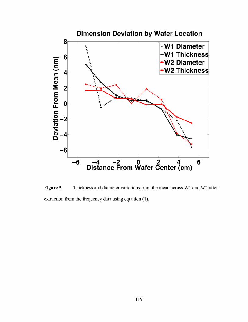
119
Figure 5 Thickness and diameter variations from the mean across W1 and W2 after
extraction from the frequency data using equation (1).
6 4 2 0 2 4 6
6
4
2
0
2
4
6
8
Distance From Wafer Center (cm)
Dev
iatio
n Fr
om M
ean
(nm
)
Dimension Deviation by Wafer Location
W1 DiameterW1 ThicknessW2 DiameterW2 Thickness
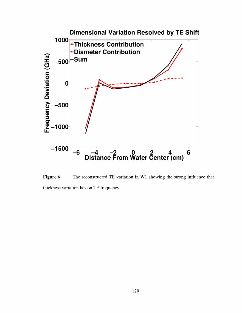
120
Figure 6 The reconstructed TE variation in W1 showing the strong influence that
thickness variation has on TE frequency.
6 4 2 0 2 4 61500
1000
500
0
500
1000
Distance From Wafer Center (cm)
Fre
quen
cy D
evia
tion
(GH
z)
Dimensional Variation Resolved by TE Shift
Thickness ContributionDiameter ContributionSum

121
Figure 7 The average dimensional variation within the dice shows that diameter
variations are consistent from wafer to wafer leading to investigation of the mask error
special cause.
0 50 100 150 200 250 3000.4
0.3
0.2
0.1
0
0.1
0.2
0.3
0.4
Within Die Distance (µm)
Dim
ensi
on D
evia
tion
(nm
)
Within Chip Dimension Deviation
W1 DiameterW1 ThicknessW2 DiameterW2 Thickness
122
Figure 8 After residual analysis to remove the special cause variation the diameter
is controlled to within +/-4Å on a die.
1 0.5 0 0.5 1
0.01
0.1
0.5
0.9
0.99
Diameter Deviation From Mean (nm)
Pro
babi
lity
Probability Plot of Within Die Width Variation
Uncorrected FitCorrected Fit Uncorrected Corrected
123
come from the same distribution. In this case, the anova is being used to assess the
probability that there is an absence of special cause variation.) [16]
When data is driven by a special cause then we may attempt to remove that
variation by performing a residual analysis [16]. The residual analysis on this data was
done using a polynomial fit of the trend from die to die. The data is then subtracted from
the fitted line giving each point a residual value. The normal probability of occurrence for
the dimensions are shown in Figure 8; the probability plots show the uncorrected
diameter data and corrected diameter data indicating the improvement of the Gaussian
nature after residual analysis is performed. It also shows that the distribution for the
corrected data is tighter. Analysis of the lithographic mask production showed that the
drawn error of the mask computer aided design (CAD) file is +/-0.7nm due to the grid
snap error on the printed silicon feature, which is close to the error between the average
mismatch from disk 1 to disk 2. Other physical special cause or even process variations
arising in mask manufacture may be attributed to the variation in the other three disks
because even process errors on the mask would turn into special causes in the fabrication
facility. Modern HVM fabs use ebeam cut masks with smaller snap resolution. It is
conceivable that this error could be mitigated in such facilities. Therefore, the residual
probability plot of diameter corrected data (black dots) in Figure 8 is a good estimate of
the achievable WID diameter variation within our manufacturing process.
An anova test and residual analysis were also performed on the thickness data.
The anova test shows a confidence value of 0.8, a high confidence that the thickness data
comes from the same distribution and not providing justification for using residual
analysis. In Figure 9 frequency probability plots of the within die frequency variation
124
reconstituted from corrected dimensional data using equation (1) are done for uncorrected
data, width corrected data and, for completeness, thickness corrected data as well.
Figure 10 gives the diameter corrected plot in histogram format. The thickness variation
may in fact be caused by a trend as we see in Figure 5 from the top to the bottom of the
wafer, but this could not be confirmed across 300µm. Not surprisingly, even though we
can improve the diameter contribution by a factor of 1/3 through elimination of
special cause variation, it does not improve the within die frequency variation by more
than about 10%, as most of the frequency variation is caused by SOI thickness variation.
125
Figure 9 After residual analysis on the diameter variation, 105GHz frequency
variation is found to be the capability of our process. When thickness is also corrected the
deviation drops to close to 70GHz, but evidence of a special cause driving the thickness
variation was not found.
50 0 50 100
0.01
0.1
0.5
0.9
0.99
Frequency Deviation From Mean (GHz)
Pro
babi
lity
Probability Plot of Within Die Frequency Variation
Uncorrected FitDiameter Corrected FitDiameter & Thickness Corrected Fit Uncorrected Diameter Corrected Diameter & Thickness Corrected
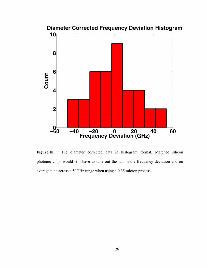
126
Figure 10 The diameter corrected data in histogram format. Matched silicon
photonic chips would still have to tune out the within die frequency deviation and on
average tune across a 50GHz range when using a 0.35 micron process.
60 40 20 0 20 40 600
2
4
6
8
10
Frequency Deviation (GHz)
Cou
nt
Diameter Corrected Frequency Deviation Histogram
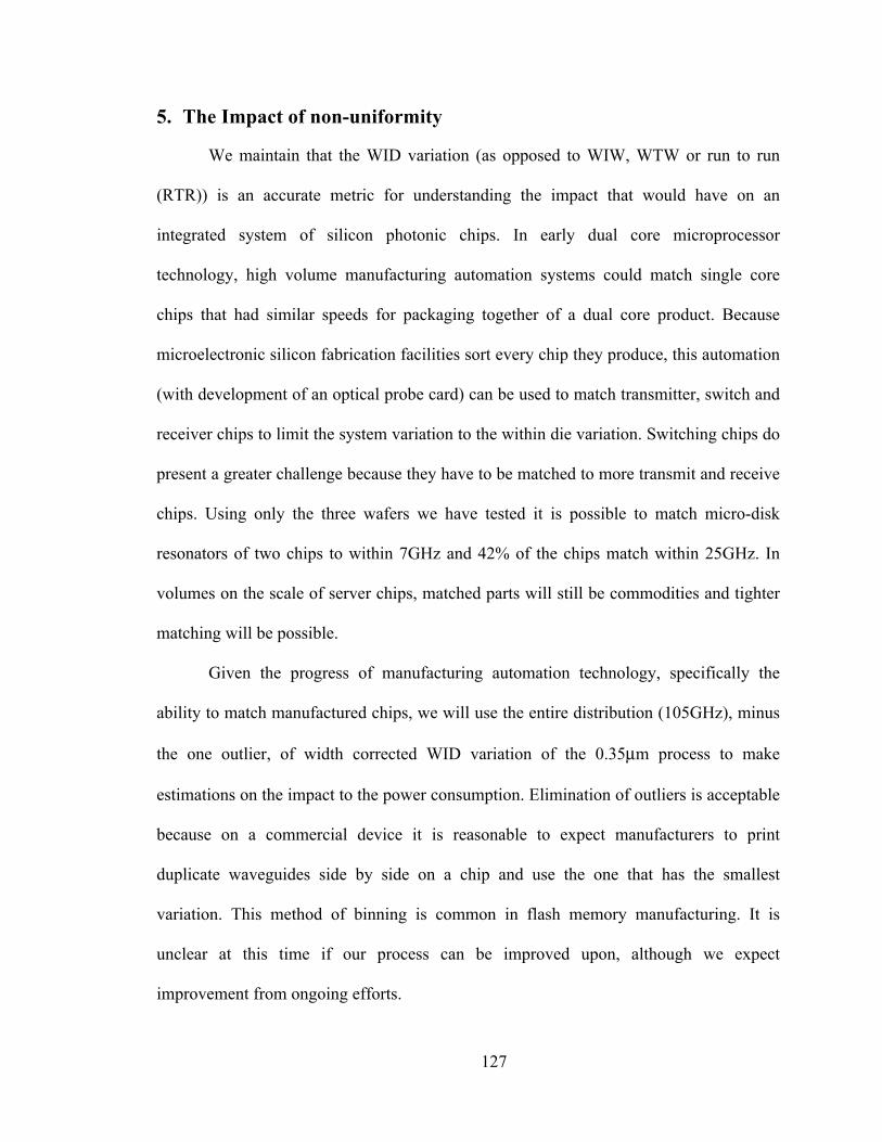
127
5. The Impact of non-uniformity
We maintain that the WID variation (as opposed to WIW, WTW or run to run
(RTR)) is an accurate metric for understanding the impact that would have on an
integrated system of silicon photonic chips. In early dual core microprocessor
technology, high volume manufacturing automation systems could match single core
chips that had similar speeds for packaging together of a dual core product. Because
microelectronic silicon fabrication facilities sort every chip they produce, this automation
(with development of an optical probe card) can be used to match transmitter, switch and
receiver chips to limit the system variation to the within die variation. Switching chips do
present a greater challenge because they have to be matched to more transmit and receive
chips. Using only the three wafers we have tested it is possible to match micro-disk
resonators of two chips to within 7GHz and 42% of the chips match within 25GHz. In
volumes on the scale of server chips, matched parts will still be commodities and tighter
matching will be possible.
Given the progress of manufacturing automation technology, specifically the
ability to match manufactured chips, we will use the entire distribution (105GHz), minus
the one outlier, of width corrected WID variation of the 0.35µm process to make
estimations on the impact to the power consumption. Elimination of outliers is acceptable
because on a commercial device it is reasonable to expect manufacturers to print
duplicate waveguides side by side on a chip and use the one that has the smallest
variation. This method of binning is common in flash memory manufacturing. It is
unclear at this time if our process can be improved upon, although we expect
improvement from ongoing efforts.
128
Modern HVM will provide improvement to the overall uniformity, although what
specific improvements we can expect is unclear because tool and technique advances to
make rectangular transistors on sub 100nm thick silicon does not translate into
quantifiable gains with circular resonators using 220nm thick silicon. For example SOI
manufacturing can achieve +/-3nm thickness variation on 70nm thick 300mm wafers; for
200nm, 70 nm thick wafers have variation of about +/-7nm [17]. This seems to indicate
that the evolution in the silicon equipment industry planarization tools (from the 200mm
generation to the 300mm generation) has reduced uniformity effects for thin SOI, but
comparative values between 300mm and 200mm for thick SOI are not available.
Additionally, this is WIW data, not WID. For diameters, the International Technology
Roadmap for Semiconductors consistently specifies a 30% improvement in critical
dimension uniformity per node because gate lengths continually scale by a factor of about
30% per node [18]. This is for patterning of rectangular structures with a field length of
33mm. The ability of 193nm immersion lithography, resists, hard-masks and modern etch
equipment could not be found for circular structures. To use this data for optical
resonators would require assumptions about geometry, thickness and translation of WIW
statistics to WID statistics although there is certainly some gain to be realized from the
progress in silicon electronics. Therefore, techniques, statistics and specifications
germane to silicon photonics, such as those presented here, will be developed on the
photonic side and provide conclusive uniformity data for 250nm thick SOI on 300nm
wafers processed with tools at the 22nm node or below.
For frequency trimming, heater technology is assumed although other techniques
have been proposed [19]. In order for all of the devices based on heated micro disk/ring
129
resonators to be relevant in a thermally varying system such as a CMOS chip in a server
environment they will have to be designed so that the resonant frequency is higher than
the source when the server is running at the maximum value of the specified temperature
range. This will ensure sufficient margin to allow an integrated heater to reduce the
resonant frequency to match the source. This would place the laser line at the far left end
of Figure 10. So when the server chip environment is at its maximum temperature the
resonator at the bottom of the frequency distribution will be several GHz above the laser
source and require some amount of power to match the channel. The frequency
distribution will then dictate additional heating for the other resonators proportional to the
size of that distribution. A wider distribution creates a larger penalty. A distribution
penalty figure of merit Pò exists such that:
P! =R2"H
(2)
In this equation, R is the range of the frequency distribution (GHz) and ηH, the
heater efficiency (W/GHz). Division by 2 is used because on average we only have to
trim across half of the distribution if it is Gaussian. Note that 3σ, or some other measure
of the breadth of the data, can replace R, if outlying resonators can be disabled or
discarded without corrupting other channels. This term merely represents the breadth of
resonator frequencies that must be considered.
The impact of manufacturing non-uniformity to a resonant device can be applied
to modulators or passive filters. Modulator switching energy is insignificant because gate
level voltage switching at 12.5Gbps using only 40µW has been demonstrated [5]. What is
130
left is trimming for manufacturing variation and tuning because of thermal environmental
effects. For both trimming and tuning heater efficiency, ηH, of 4.4µW/GHz is used as
demonstrated in [10]. For trimming, assuming 105GHz frequency variation across a chip,
the distribution penalty, Pò, is 231µW. For tuning, a server environment is assumed with
an average 25OC temperature variation where we use 10GHz/OC of resonant frequency
shift. This yields 1.1mW for a grand total including modulation, trimming and tuning of
1.371mW, which means trimming represents 17% of the total power per resonant device.
Looking at the energy picture for 12.5Gbps the average power corresponds to 110fJ/bit,
which is 12% above the 2015 target given in [1]. At speeds above 14Gbps this goal
would be met.
An important outcome from this analysis is that improving heater efficiency is the
primary channel for lowering power consumption in these devices. It addresses the
largest contributor to power consumption, temperature tuning, and also indirectly, the
second largest, trimming to compensate for manufacturing variation. In addition to the
tethering technique in [10], effort to improve resonator insulation using backside etch has
been demonstrated [20]; silicon electronics research into porous dielectrics [21] and
thermally tailored sputtered oxides [22] provide further promise if optically sound
analogs can be found.
6. Summary
In evaluating the power costs of systems built with demonstrated devices in
silicon photonics, we evaluated a six inch SOI 0.35µm process to quantify the frequency
variation across runs, wafers and dice. The process has 1THz within wafer variation in
the TE mode resonance. By comparing the TE and TM resonant frequency variations in

131
microdisk resonators, it has been demonstrated that the primary driver of resonator non-
uniformity is SOI thickness variation, as opposed to diameter variations, which can
exceed 10nm across a wafer. Through the use of this technique, special cause variation
was extracted from the within die measurements and eliminated by residual analysis to
demonstrate a 105GHz range within a 300µm distance printed on a single die. Although
our process can likely be improved upon to reduce lithographic and other deleterious
patterning and processing effects, SOI thickness nonuniformity remains the primary
driver of resonant frequency nonuniformities in microdisk resonators.
Based on this result the estimated non-uniformity driven power consumption is
231µW which when added to thermal tuning for environmental considerations is 17% of
the total power consumed per resonant device. This result applies to both modulators and
passive filters. Therefore, the largest impact to reducing power consumption in resonant
silicon devices will come from improvements in thermal tuner efficiency.
132
7. References
1. D.A.B. Miller, “Device Requirements for Optical Interconnects to Silicon Chips” Proceedings of the IEEE Vol 97 No 7 1166-1185 (2009)
2. P. M. Kogge (editor), "ExaScale Computing Study: Technology Challenges in Achieving Exascale Systems," Univ. of Notre Dame, CSE Dept. Tech. Report TR-2008-13, Sept. 28, 2008
3. Q. Xu, B. Schmidt, S. Pradhan and M. Lipson, “Micrometre-scale silicon electro-optic modulator”, Nature, Vol. 435, pp. 325-327, 19 May 2005
4. P. Dong, S. Liao, D. Feng, H. Liang, D. Zheng, R. Shafiiha, C.-C. Kung, W. Qian, G. Li, X. Zheng, A. V. Krishnamoorthy, and M. Asghari, “Low Vpp, Ultralow-Energy, Compact, High-Speed Silicon Electro-Optic Modulator,” Optics Express, Vol 17, 25, 22484-22490 (2009)
5. W. A. Zortman, Michael R. Watts, Douglas C. Trotter, Ralph W. Young and Anthony L. Lentine, “Low-Power High-Speed Silicon Microdisk Modulators,” (CLEO) CThJ4 San Jose, Ca (2010)
6. M. R. Watts, D. C. Trotter, and R. W. Young, "Maximally Confined High-Speed Second-Order Silicon Microdisk Switches," in Optical Fiber Communication Conference and Exposition and The National Fiber Optic Engineers Conference, OSA Technical Digest (CD) (Optical Society of America, 2008), paper PDP14
7. B. G. Lee, A. Biberman, J. Chan, K. Bergman, "High-Performance Modulators and Switches for Silicon Photonic Networks-on-Chip [invited]," IEEE Journal of Selected Topics in Quantum Electronics 16 (1) 6-22 (2010)
8. A. Biberman, H. L. R. Lira, K. Padmaraju, N. Ophir, M. Lipson, K. Bergman, "Broadband CMOS-Compatible Silicon Photonic Electro-Optic Switch," CLEO CPDA11 (2010)
9. A. Barkai, Y. Chetrit, O. Cohen, R. Cohen, N. Elek, E. Ginsburg, S. Litski, A. Michaeli, O. Raday, D. Rubin, G. Sarid, N. Izhaky, M. Morse, O. Dosunmu, A. Liu, L. Liao, H. Rong, Y. H. Kuo, S. Xu, D. Alduino, J. Tseng, H. F. Liu, and M. Paniccia, “Integrated Silicon Photonics for Optical Networks,” Journal of Optical Networking, Vol 6, Issue 1, 25-47 (2007)
10. M. R. Watts, W. A. Zortman, D. C. Trotter, G. N. Nielson, D. L. Luck, R. W. Young, “Adiabatic Resonant Microrings (ARMs) with Directly Integrated Thermal Microphotonics,” CLEO CPDB10 (2009)
11. C. T. DeRose, M. R. Watts, D. C. Trotter, D. L. Luck, G. N. Nielson, and R. W. Young, "Silicon Microring Modulator with Integrated Heater and Temperature Sensor for Thermal Control," in Conference on Lasers and Electro-Optics, OSA Technical Digest (CD) (Optical Society of America, 2010), paper CThJ3
12. P. Dong, S. Liao, D. Feng, H. Liang, R. Shafiiha, N. Feng, G. Li, X. Zheng, A. V. Krishnamoorthy, and M. Asghari, "Tunable High Speed Silicon Microring Modulator," in Conference on Lasers and Electro-Optics, OSA Technical Digest (CD) (Optical Society of America, 2010), paper CThJ5
13. W. A. Zortman, M. R. Watts, and D. C. Trotter, "Determination of Wafer and Process Induced Resonant Frequency Variation in Silicon Microdisk-Resonators," in Integrated Photonics and Nanophotonics Research and Applications, OSA Technical Digest (CD) (Optical Society of America, 2009), paper IMC5
133
14. M. R. Watts, D. C. Trotter, R. W. Young, and A. L. Lentine, “Ultralow power silicon microdisk modulators and switches,” Proceedings of IEEE conference on Group IV Photonics (Institute of Electrical and Electronics Engineers, New York, 2008), pp. 4–6, 2008.
15. M. Popović, “Complex-frequency leaky mode computations using PML boundary layers for dielectric resonant structures,” Integrated Photonics Research, Washington, DC, ( 2003)
16. R. E. Walpole and R. H. Meyers, “Probability and Statistics for Engineers and Scientists,” Macmillan, New York (1989)
17. Soitec products page: http://www.soitec.com/en/products/soi-products.php 18. International Technology Roadmap for Semiconductors 2009:
http://www.itrs.net/Links/2009ITRS/Home2009.htm 19. D. K. Sparacin, C.-Y. Hong, L. C. Kimerling, J. Michel, J. P. Lock, and K. K.
Gleason, "Trimming of microring resonators by photo-oxidation of a plasma-polymerized organosilane cladding material," Opt. Lett. 30, 2251-2253 (2005)
20. John E. Cunningham, Ivan Shubin, Xuezhe Zheng, Thierry Pinguet, A. Mekis, Y. Luo, H. Thacker, G. Li, J. Yao, K. Raj, and A. V. Krishnamoorthy, "Highly-efficient thermally-tuned resonant optical filters," Opt. Express 18, 19055-19063 (2010)
21. Y. Zhu, T. E. Müller, J. A. Lercher, “Single Step Preparation of Novel Hydrophobic Composite Films for Low-k Applications,” Advanced Functional Materials, Vol. 18 (21) 3427-2433 (2008)
22. S. M. Lee, D. G. Cahili, and T. H. Allen, “Thermal conductivity of sputtered oxide film,” Phys. Rev. B 52, 253-257 (1995)
134
Chapter Five: Long Haul Performance
1. Introduction
As presented in Chapter 2, recent work in silicon photonics has focused on
creating compact filters, modulators and detectors for dense integration on CMOS or a
photonic chip later bonded to CMOS [1,2,3,4]. This waveguide-coupled technology
offers the potential to integrate complex functions consisting of many devices for low
energy/bit scalable arrays of interconnects on a silicon platform. Data rates above 10Gbps
have been demonstrated for short haul wavelength division multiplexed (WDM)
interconnects as an alternative to parallel Vertical Cavity Surface Emitting Laser
(VCSEL) based links used in datacenter and supercomputer server networks. While it can
be expected that silicon Mach Zehnder modulators would be applicable to long distance
communications, recent measurements of silicon resonant microphotonic modulators
have shown their potential for geographically separated interconnects which, among
many other applications, could enable multi-datacenter virtualization using the same
transmit and receive chips proposed for server short link communication [5,6]. In this
work we measure the long distance dispersion characteristics of low power microdisk
technology and explain the low power penalties with a well-known resonator model.
135
Other work (subsequent to the data reported on here) on long haul transmission
using resonant silicon technology [6] which does not include a physical model that
corroborates with measurements and the short pseudorandom bit sequence (PRBS) of 27-
1 is not predictive for the commonly used G.709 Optical Transport Channel Unit-2
protocols operating at 10Gbps that are approximated more accurately with longer bit
sequences. Thus, the shorter bit sequence can potentially lead to less dispersion penalties
as measured in [6] than would be achieved in an actual long distance systems and less
than the measurements that we report here. Here, we measure the long distance
dispersion characteristics of low power microdisk technology and in consideration of the
application use a more stringent 231-1 PRBS. Results are for the first time substantiated
with a resonator model.
The disks are of the 3.5µm diameter variety as described in Chapter 2 and
reviewed here. The process uses 240nm thick silicon on insulator with a 350nm bus to
waveguide separation. Contact is made using tungsten to highly doped P and N ohmic
regions with PN junction overlap in a vertical depletion region. The reader may find
Figures 1 and 2 helpful for review. The advantage of this design is that by using reverse
bias modulation in a compact design record low energy/bit is achieved [7] and no pre-
emphasis is needed. Furthermore, disks suffer from fewer manufacturing variations than
rings because there is no inner radial dimension or etch-depth sensitive super-radial
contact area [8]. Modulation here is 3.5V peak-to-peak reverse bias.
136
Figure 1 Top view shows the PN junction occupies pi-radians of the disk and the
ohmic contacts are half moon shaped mirroring the disk circumference.

137
Figure 2 Modulator side view shows it is a vertical depletion device, side coupled
to a bus waveguide and designed to run in reverse bias. P-type doping is on top, N-type
on the bottom with highly doped plugs in the center.

138
2. Analysis
When considering the long distance transmission, a simple first order
phenomenological model for a critically coupled resonator [9] is used to describe the
transmitted waves:
st =j(! !!0 (t))
j((! !!0 (t))+1
" (t)
si
(1)
where si is the source wave amplitude incident at the disk-waveguide point, st is the
through-port (or transmitted) wave amplitude, ω is the frequency of the CW laser line
incident on the resonator, ω0 is the resonant frequency of the disk, and τ is the photon
lifetime. Both ω0 and τ are functions of the voltage applied across the modulator. Figure
1 distinguishes the incident and transmitted ports for si and st respectively. For a
modulator with no drop waveguide, which is the case being considered, we are only
interested in the transmitted wave. Under modulation this is a pulse with amplitude given
by equation (1) and phase, φ, given by the component analysis of equation (1):
! = tan!1 " (V ) ! !!0 V( )"# $%{ } (2)
By inspection of equation (2) it is clear that when ω=ω0 the phase term is zero
and that the phase changes to higher values as the resonance (ω0) moves to lower
frequencies away from the laser frequency allowing the laser wave to pass creating a
logic “1”. This movement of the resonance to lower frequencies causes the value of ω-ω0
139
to increase leading to an increase in the argument of the arctan function. This is a phase
increase, or phase accumulation. The chirp, defined as dφ/dt, is then positive. The
opposite action happens as the modulator resonance moves back onto the laser line
(carrier frequency). So there is positive chirp in the leading edge of the pulse and
negative chirp in the trailing edge meaning the pulse must be negatively chirped. This
action of the phase can be seen in Figure 3 where the phase response of the modulator is
plotted for two different resonances. Movement of ω0 by 20GHz results in a phase shift
of about ½ a radian for constant frequency, ω, which is the carrier wave emanating from
a laser source. Because of the accumulated phase during this operation, higher
frequencies are in the pulse leading edge.
To quantify this action, the resonances were measured at 0V, a logic “0”, and
also at -3.5V, a logic “1”. Plots of the resonances of these two states are shown in figure
4. The 3.5V reverse bias point shows a higher Q because of the longer photon lifetime
possible when carriers are swept out of the disk in reverse bias. The values of the photon
lifetime at the two points are estimated using the 3dB width of the resonance to be 5.2ps
and 5.9ps for 0V and -3.5V respectively. The resonant frequencies and photon lifetimes
at these bias points were then used as endpoints for the sweep of ω0 and τ in equation (1).
To simulate the forcing between these endpoints a time constant was computed from the
device series resistance and capacitance to emulate the charge depletion action in the
resonator. The pulse and temporal phase as predicted by equation (1) is depicted in
Figure 5. The model also predicts a phase evolution with high frequencies at the leading
edge and lower frequencies at the trailing edge, which are consistent with the theoretical
study done in [10]. The change from higher frequency to lower frequency during the
140
duration of the pulse is evident and this will cause pulse compression in standard SMF-28
fiber which has a dispersion coefficient of ~18ps/nm-km for 1550nm light.
For example, consider a resonator in which τ is held constant. In the case of the
modulator considered that is not the case, however the change is small and holding it
constant simplifies the example. When the resonance is on the carrier frequency, before a
“1” is created the phase is 0 because the argument of the arctan is 0. When the frequency
of the resonator is tuned to a frequency 20GHz below the laser frequency, that is ω0 now
resides 20GHz below ω, the argument of the arctan function becomes 20GHz X τ. The
value of τ is 5.2ps. So the argument is 0.104. The value of arctan(0.104) is 5.9. The chirp
is dφ/dt(1/2π). If the resonator switches in 20ps time (the full rise time of the pulse) then
the chirp is 9.3GHz for the leading edge of the pulse and when integrated over the 200ps
of say a 5Gbps pulse gives 46MHz. The negative phase accumulation in the trailing edge
can be estimated in the same way and if the same switching time is assumed the total is
92MHz. The results for the actual modulator reported on in this chapter were numerically
integrated and resonance shifting was only about 18GHz.
Once the chirp has been calculated the full power penalty can be calculated. To
estimate the resulting power penalties, reference is made to [11] for two equations. (The
power penalty in this case refers to the additional optical power, provided by an erbium
doped fiber amplifier, needed in the receiver in order to keep the bit error rate constant
for an increase in the transmission distance at a given bit rate.) The first predicts the
power penalty based on pulse spreading of a Gaussian pulse for given bit-rate, B,
dispersion, D, length, L, and laser linewidth, σλ:

141
(3)
The model output becomes imaginary when the inner parenthesis grows beyond
unity so use of this equation is limited to bit-rates below 6Gbps. The second equation
employed provides a power penalty for the chirp alone which we convert to wavelength
for λc:
!c = "10log10 1" 4BLD#$c[ ] (4)
The values for B, L and D are known from the experiment and fiber characteristic
given above. σλ is estimated to be ¾ of the bit rate, which accounts for the frequency side
bands on the amplitude modulated carrier wave. This leaves the chirp, λc, which we
estimate by integrating the values from Figure 5 over the length of the pulse to get
70MHz (~560fm near 1550nm) in the frequency domain for the pulse at 5Gbps and
approximately twice that at 10Gbps.
The results of equation (3) and (4) are added phenomenologically to account for
the two contributors to power penalty. In the regime where high frequencies lead the
pulse equation (2) predicts compression in SMF-28 fiber leading to the analytically
predicted power penalties in Figure 6 that will be used in comparison to measured data.
The plot shows no power penalty at 40km for 5Gbps operation and a 1dB penalty at
70km, which is also consistent with the theoretical values shown in [5].
!
"d = #5log10 1# 4BLD$%( )2[ ]
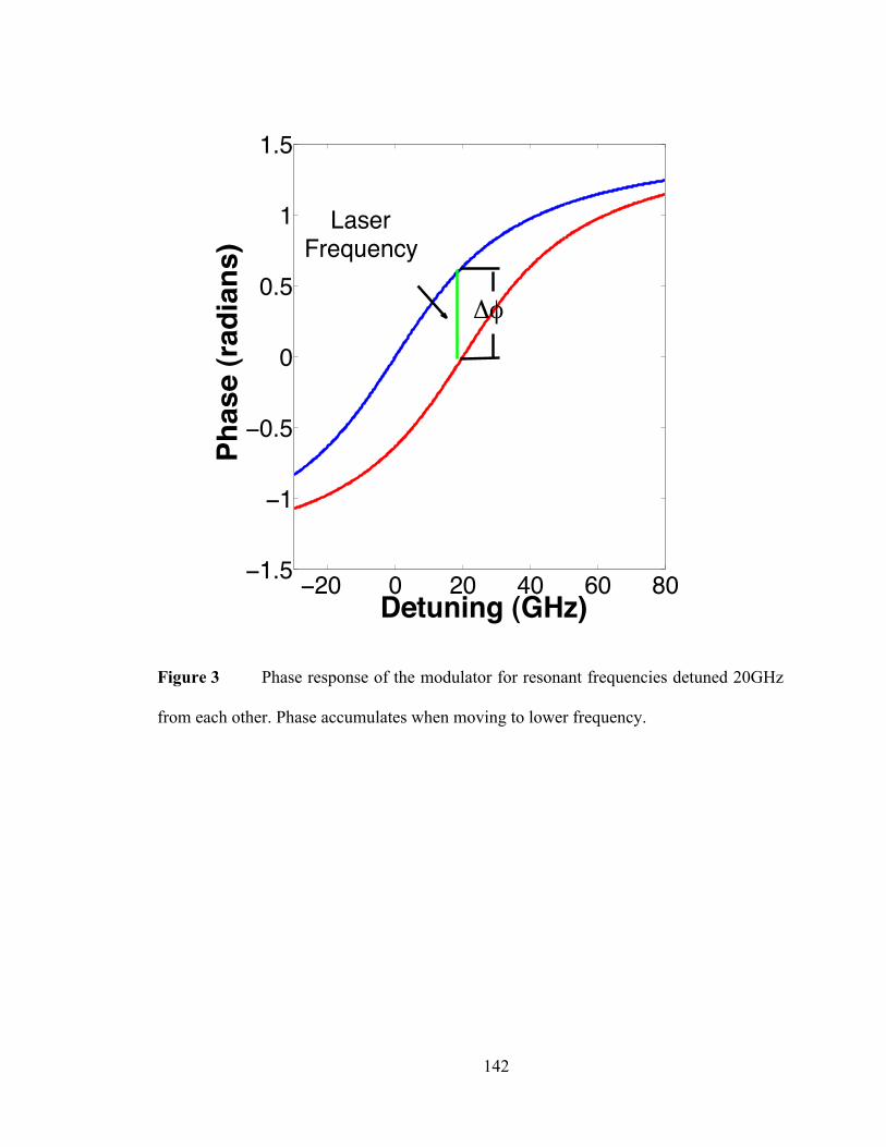
142
Figure 3 Phase response of the modulator for resonant frequencies detuned 20GHz
from each other. Phase accumulates when moving to lower frequency.
20 0 20 40 60 801.5
1
0.5
0
0.5
1
1.5
Detuning (GHz)
Pha
se (r
adia
ns)
LaserFrequency

143
Figure 4 Resonances for 0V and 3.5V reverse bias. The source laser is tuned to the
resonance (minimum) of the red curve for a logic “0” (i. e. ~20 GHz on the plot above)
20 0 20 4015
10
5
0
Frequency (GHz)
Los
s (d
B)
0 (0V)
0 ( 3.5V)
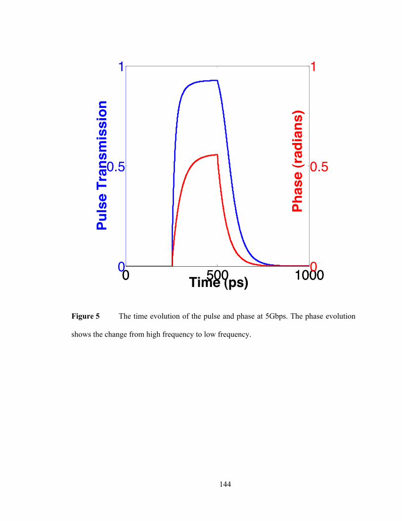
144
Figure 5 The time evolution of the pulse and phase at 5Gbps. The phase evolution
shows the change from high frequency to low frequency.
0 500 10000
0.5
1
Puls
e Tr
ansm
issi
on
0 500 10000
0.5
1
Phas
e (r
adia
ns)
Time (ps)
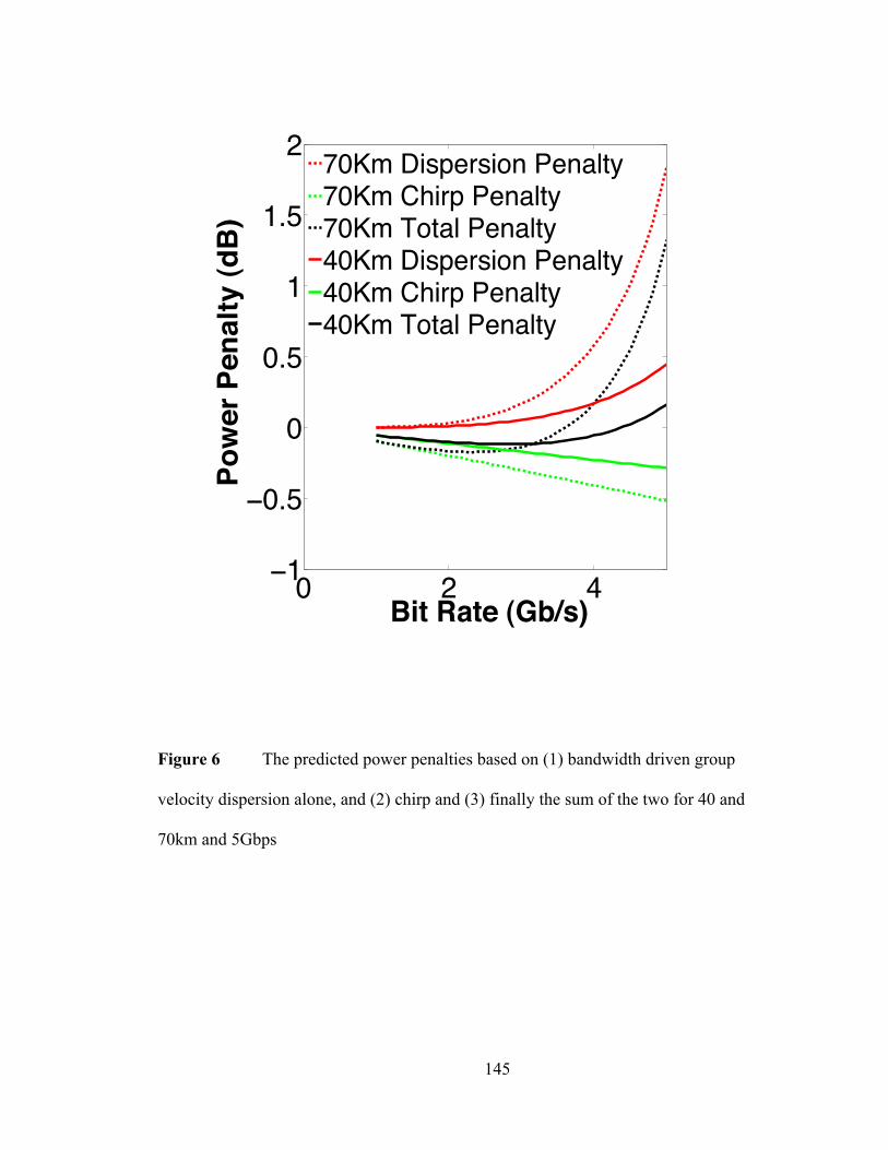
145
Figure 6 The predicted power penalties based on (1) bandwidth driven group
velocity dispersion alone, and (2) chirp and (3) finally the sum of the two for 40 and
70km and 5Gbps
0 2 41
0.5
0
0.5
1
1.5
2
Bit Rate (Gb/s)
Pow
er P
enal
ty (d
B)
70Km Dispersion Penalty70Km Chirp Penalty70Km Total Penalty40Km Dispersion Penalty40Km Chirp Penalty40Km Total Penalty
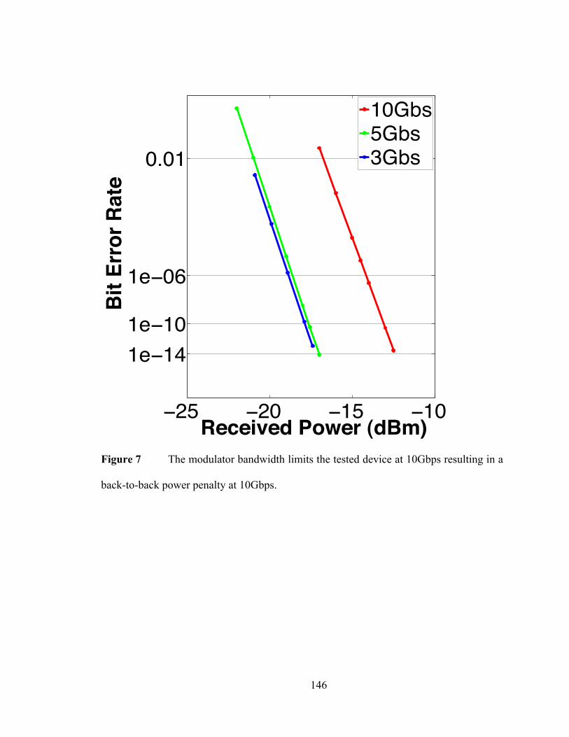
146
Figure 7 The modulator bandwidth limits the tested device at 10Gbps resulting in a
back-to-back power penalty at 10Gbps.
25 20 15 10
1e 141e 10
1e 06
0.01
Received Power (dBm)
Bit
Erro
r Rat
e
10Gbs5Gbs3Gbs
147
3. Experimental Results
Before looking at the power penalty measured performance at 40km and 70km
it is necessary to understand the bandwidth limitation of the modulator. Figure 7 shows
that no bandwidth limitation exists up to 5Gbps for back-to-back operation of the
modulator and detector. At 10Gbps the bandwidth limitation, which manifests itself as a
power penalty in back-to-back measurements, results from a 30fF capacitance from 50µm
probe pads coupling to the silicon substrate.
Measurements were done using the setup shown in Figure 8. The Centellax TG-
1B1A contained the pattern generator, clock and bit-error-rate tester (BERT). Light was
coupled from an Agilent 8164B tunable laser source into the photonic chip using
Nanonics lensed fibers with a total on/off chip insertion loss of ~20dB. The signal was
amplified before and after the intervening fiber length to 0dBm in both cases and then
attenuated before the receiver in order to vary the received power.
Results for the measurements are shown in Figures 9 and 10. The 5Gbps data
shows consistency with the model and show no power penalty at 40km. The results at
70km are also within 0.5dB of the prediction for a measured penalty of 1dB. Larger
power penalties are observed for 10Gbps modulation yet only about 1dB is seen at 40km
with 6.5dB measured at 70km. Prediction for the 10Gbps performance is not included
because the logarithmic nature of equation (3) precludes prediction beyond about 6Gbps.
The performance is compared to a lithium niobate Mach Zehnder Modulator
(MZM) in figures 11 and 12. The 5Gbps performance is within 0.5dB of the MZM out to
70 km. The MZM shows an insignificant penalty at this distance. The MZM penalty is
only 2.5dB as compared to 6.5dB for the resonator at 10Gbps. The 5Gbps data and the
148
modeling of pulse compression in the disk modulator type indicate the potential for
competitive performance at 10Gbps with mitigation or elimination of probe pad
capacitance.
In summary, silicon photonic microdisk resonators have been demonstrated for
long distance applications and a simple model explaining the low power penalties in the
non-bandwidth limited case (5 Gbps) given. A first order model analyzed for the phase
change across the pulse predicts 70MHz of negative chirp in a 200ps pulse. The negative
chirp imposed by the modulator results in pulse compression in SMF-28 fiber which
leads to no power penalty at 40km and 0.5dB penalty at 70km. Additionally, the devices
show promise for distributed computing applications with power penalties comparable to
installed long distance modulation technology at 5Gbps and the potential for similar
performance at 10Gbps, assuming a reduction of stray parasitic capacitances.
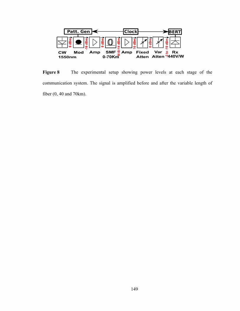
149
Figure 8 The experimental setup showing power levels at each stage of the
communication system. The signal is amplified before and after the variable length of
fiber (0, 40 and 70km).

150
Figure 9 The measured power penalties for 0Km, 40Km and 70Km at of 0dB, 0dB
and 1dB respectively at 5Gbps are in agreement with theory indicating that the modulator
does benefit in this regime from negative chirp.
25 20 15 10
1e 141e 10
1e 06
0.01
Received Power (dBm)
Bit
Erro
r Rat
e
0Km40 Km70 KmModel 40 kmModel 70 km
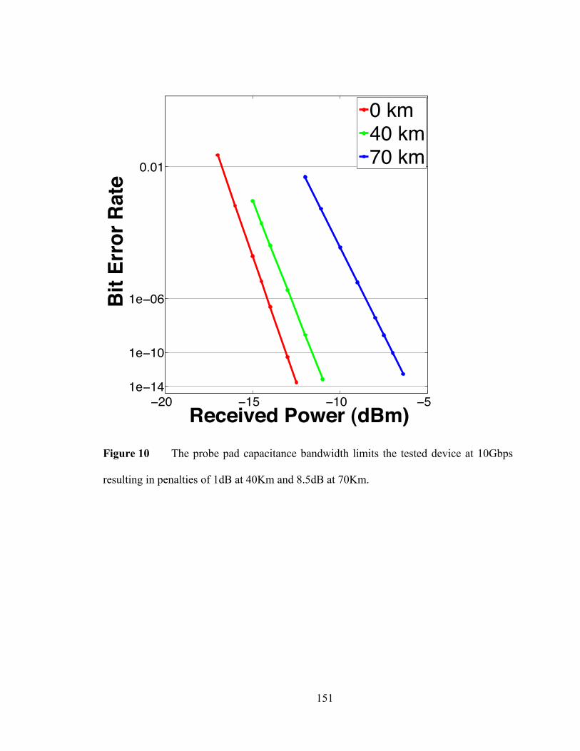
151
Figure 10 The probe pad capacitance bandwidth limits the tested device at 10Gbps
resulting in penalties of 1dB at 40Km and 8.5dB at 70Km.
20 15 10 51e 14
1e 10
1e 06
0.01
Received Power (dBm)
Bit
Erro
r Rat
e
0 km40 km70 km
152
Figure 11 Comparison to a Mach Zehnder Modulator at 5Gbps. The results are
favorable, showing only ½ dB power penalty at difference at 70Km.
153
Figure 12 Comparison to a Mach Zehnder Modulator at 10Gbps. The results are
consistent with the bandwidth limitation shown earlier.
154
4. References
1. Q. Xu, B. Schmidt, S. Pradhan and M. Lipson, Micrometre-Scale Silicon Electro-Optic Modulator, Nature, Vol. 435, pp. 325-327, 19 May 2005
2. M. R. Watts, D. C. Trotter, and R. W. Young, "Maximally Confined High-Speed Second-Order Silicon Microdisk Switches," Optical Fiber Communication Conference, OSA, San Diego (2008) PDP14
3. A. Alduino, L. Liao, R. Jones, M. Morse, B. Kim, W. Lo, J. Basak, B. Koch, H. Liu, H. Rong, M. Sysak, C. Krause, R. Saba, D. Lazar, L. Horwitz, R. Bar, S. Litski, A. Liu, K. Sullivan, O. Dosunmu, N. Na, T. Yin, F. Haubensack, I. Hsieh, J. Heck, R. Beatty, H. Park, J. Bovington, S. Lee, H. Nguyen, H. Au, K. Nguyen, P. Merani, M. Hakami, and M. Paniccia, "Demonstration of a High Speed 4-Channel Integrated Silicon Photonics WDM Link with Hybrid Silicon Lasers," in Integrated Photonics Research, Silicon and Nanophotonics, OSA (2010), paper PDIWI5.
4. N. N. Feng, S. Liao, Dazeng Z. Feng, P. Dong, D. W. Zheng, H. Liang, R. Shafiha, G. L. Li, J. E. Cunningham, A. V. Krishnamoorthy, M. Ashgari, "High speed carrier-depletion modulators with 1.4V-cm VπL integrated on 0.25µm silicon-on-insulator waveguides," Opt. Express 18, 7994-7999 (2010)
5. W.A. Zortman, A. L. Lentine, M. R. Watts, D. C. Trotter, "Power penalty measurement and frequency chirp extraction in silicon microdisk resonator modulators," Optical Fiber Communication (OFC/NFOEC), San Diego 21-25 March 2010
6. Aleksandr Biberman, Sasikanth Manipatruni, Noam Ophir, Long Chen, Michal Lipson, and Keren Bergman, "First demonstration of long-haul transmission using silicon microring modulators," Opt. Express 18, 15544-15552 (2010)
7. R. Soref, B. Bennett, "Electrooptical effects in silicon," Quantum Electronics, IEEE Journal of , vol.23, no.1, pp. 123- 129, Jan 1987
8. William A. Zortman, Michael R. Watts, Douglas C. Trotter, Ralph W. Young and Anthony L. Lentine, “Low-Power High-Speed Silicon Microdisk Modulators,” (CLEO) CThJ4 San Jose, Ca (2010)
9. B. E. Little, S. T. Chu, H. A. Haus, J. Foresi and J. P. Laine, “Microring Resonator Channel Dropping Filters,” Journal of Lightwave Technology, Vol. 15, No. 6, June 1997
10. Lin Zhang, Yunchu Li, Jeng-Yuan Yang, Muping Song, R. G. Beausoleil, R.G., A.E. Willner, "Silicon-Based Microring Resonator Modulators for Intensity Modulation," IEEE Selected Topics in Quantum Electronics, vol.16, no.1, pp.149-158, Jan.-feb. 2010
11. G. P. Agrawal, “Fiber-Optic Communication Systems,” p. 210, John Wiley and Sons, Third Edition, New York, 2002
155
Chapter Six: Conclusion
The dissertation began with a review of projected bandwidth requirements for
HPC targeted server chips. Conclusions were drawn based on consideration of the
continuing evolution of electrical signaling, 3D interconnect and materials used in chip
processing. Off-chip and on-chip bandwidth can be handled electronically with the chip-
to-chip portion handed off to a 3D integrated photonic chip through the use of through
silicon via’s. Off-chip interconnect will continue to increase with a WDM solution
required in the 2018 timeframe.
The proposed solution is WDM silicon photonics and the work presents a
transmitter with single femto-joule per bit operation, LVDS compatible voltage levels,
demonstrated integration with CMOS, manufacturability and capability for long haul
interconnect.
Single femto-joule per bit operation is obtained partially through the AC coupling
technique (forward and reverse bias), but also because of the arrangement of the
implants. Other technologies in this field employ horizontal depletion regions. Because of
the modal shape in ring or disk as illustrated in chapter 4, a horizontal depletion region
156
provides greater modal interaction and requires less energy. Much effort, a description of
which will be in future publication, was devoted to tailoring dopant energies to maximize
this effect.
The remaining points are best gathered under the banner of integration of applied
research into an existing market. The implementation of LVDS is very important. Prior to
this 1V and even 900mV operation was demonstrated with reasonable extinction.
However, these levels provide very little margin for designers. It is important when doing
applied research that not only the ultimate application be considered, but the ecosystem it
exists in. This includes the designers, fabs and integration with off-the-shelf parts. So in
addition to LVDS, monolithic integration with CMOS and a thorough investigation of
manufacturing are available. Monolithic integration shows the potential for electrical
multiplexing on the silicon chip (time division multiplexing of the electrical signal). The
manufacturing assessment is, in a word, done. The community of silicon photonics
researchers now has a basis for supporting supply of these parts in high volume. One
issue, which was not broached, was the Q variation of these devices. Initial work has
shown that this is not significant. A future publication exploring process variation further
will explore this in more detail. Finally, while long haul transmission is not central to the
thesis of providing low power chip to chip interconnects, its demonstration shows the
general compatibility of these parts with existing photonics.
While records were broken and many initial demonstrations achieved in this
work, the fundamental contribution is the engineering of an external modulator to work
within the existing framework of product design and manufacturing, followed by
insertion into large existing and planned systems.
157
There are several pieces that still remain to be demonstrated in a transmitter. They
include integrated heating, multichannel operation and a method for controlling the
temperature and resonance of the device should a suitable heater be designed. An
additional consideration is designing an optical package so that fibers can be attached
with low loss interface. Optical packaging should be an outgrowth of current techniques
for lasers and other fiber attached equipment.
The other half of the communication link is of course the WDM receiver,
specifically a filter and detector. For filters the challenge is similar to that of the
modulator in that a tuning mechanism, probably thermal, is needed for filters. The
detector is a more difficult problem because of the requirement for most detectors to use
an amplifier to get enough voltage to flip an inverter. Leading edge CMOS inverters will
have to be designed to convert the small detector current into a voltage that can cause an
inverter state to flip without the large power requirements typical in a trans-impedance
amplifier.
There are of course many ways to implement a WDM system that can handle the
bandwidth necessary to handle the chip-to-chip communication of future chip
multiprocessors. However, few have all of the qualities necessary for this job. These
include intimate integration with CMOS, manufacturability in volumes to match server
chips 1:1, low power, high bandwidth and the compactness to fit the system on a 2cm2
chip. It is for these reasons that silicon photonics is a very promising technology to fulfill
this role should solutions be found to the challenges mentioned above.