white paper oe-a roadmap for organic and printed electronics · and electroluminescent and oled...
TRANSCRIPT

A working group within
3rd Edition
White Paper
OE-A Roadmap for Organicand Printed Electronics


OE-A ROADMAP FOR ORGANIC AND PRINTED ELECTRONICS, 3rd EDITION
Table of Contents 1 Executive Summary ..................................................................................................................1 2 About the OE-A Roadmap ........................................................................................................4 3 Introduction ...............................................................................................................................5 4 Applications...............................................................................................................................6
4.1 Applications Roadmap....................................................................................................8 4.1.1 Organic Photovoltaics 8 4.1.2 Flexible Display 13 4.1.3 Electroluminescent and OLED Lighting 23 4.1.4 Printed RFID 27 4.1.5 Printed Memory 32 4.1.6 Organic Sensors 35 4.1.7 Flexible Batteries 40 4.1.8 Smart Objects 42 4.1.9 Smart Textiles 46 4.1.10 Short List of Key Application Parameters 49 4.2 OE-A Roadmap for Organic and Printed Electronics Applications ..........................50
5 Technology ..............................................................................................................................51 5.1 Materials .........................................................................................................................51 5.2 Substrates ......................................................................................................................54 5.3 Printing and Patterning Techniques............................................................................57 5.4 Devices ...........................................................................................................................62 5.5 Technology Levels ........................................................................................................64 5.6 Short List of Key Technology Parameters ..................................................................65
6 Principle Challenges ...............................................................................................................66 7 Summary and Outlook ............................................................................................................68 8 Acknowledgements.................................................................................................................70 Imprint ......................................................................................................................................73
Copyright © Organic Electronics Association, OE-A, Frankfurt, 2009
All rights reserved. Reproduction only with written permission by OE-A.

OE-A ROADMAP FOR ORGANIC AND PRINTED ELECTRONICS, 3rd EDITION 1
1 Executive Summary
This white paper presents the major findings of the Organic Electronics Association’s third ver-sion of the Organic and Printed Electronics Roadmap, based on work done since the second version of the roadmap was completed in September 2007. It continues the work started in pre-vious versions but includes an updated discussion of the technical progress that has been made in the field since the last roadmap, including recent progress in improved materials, improved processes.
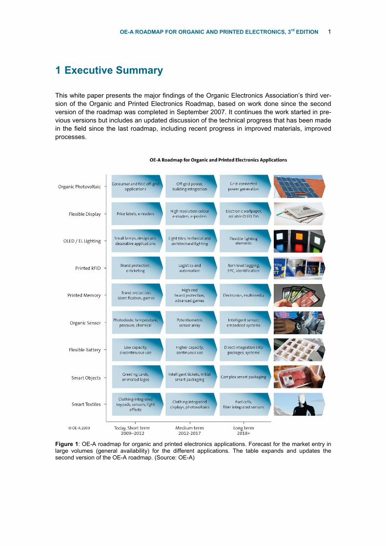
Figure 1: OE-A roadmap for organic and printed electronics applications. Forecast for the market entry in large volumes (general availability) for the different applications. The table expands and updates the second version of the OE-A roadmap. (Source: OE-A)

2 OE-A ROADMAP FOR ORGANIC AND PRINTED ELECTRONICS, 3rd EDITION
In the applications section new developments in applications are monitored and it is noted that since the last roadmap more products have started to enter the market. Two new applications are explored: smart textiles and electroluminescent (EL) and organic light emitting diode (OLED) lighting. In addition, the previous application area of display backplanes has been expanded to include flexible displays as a whole. We update our forecast for the market entry on larger scales for the various applications, and have re-examined the key application and technology parameters and principle challenges (so-called Red Brick Walls) that have been identified. In the technology section we also take account of recent progress in new materials and improved processes.
The following applications areas are addressed:
• Organic photovoltaic cells (OPV)
• Flexible displays
• Electroluminescent and OLED based lighting
• Printed RFID
• Organic memory devices
• Flexible batteries
• Organic sensors
• Smart objects (integrating several of the above functions)
• Smart textiles that integrate functionality into fabrics
The key application parameters distilled from the key parameters for each application group are identified as
• Complexity of the device
• Operating frequency of the circuit
• Lifetime/stability/homogeneity
• Operating voltage
• Efficiency
• Cost
The key technology parameters were identified as
• Mobility/electrical performance
• Resolution/registration
• Barrier properties/environmental stability
• Flexibility/bending radius
• Fit of process parameters
• Yield
Individual roadmaps were developed for each application field and are discussed in the main text of this white paper. In addition, a graphical representation of an overall roadmap for organic and printed electronics was developed, which is shown in Figure 1.

OE-A ROADMAP FOR ORGANIC AND PRINTED ELECTRONICS, 3rd EDITION 3
Based on an analysis of the application and technology parameters, the recent progress in materials and process technology and the expected future technology development, the follow-ing key challenges (“Red Brick Walls”) were identified:
• Resolution, registration and process stability of the patterning processes
• Charge carrier mobility and electrical conductivity of the semiconductor and conducting materials
• Circuit design including complementary metal oxide semiconductor (CMOS)-transistors
Thus far neither the “killer application” for organic and printed electronics nor a simple scaling law analogous to Moore’s Law could be identified for organic and printed electronics, but the development in technology and the introduction of new products gives confidence that organic and printed electronics has great potential for further growth.

4 OE-A ROADMAP FOR ORGANIC AND PRINTED ELECTRONICS, 3rd EDITION
2 About the OE-A Roadmap
Organic and printed electronics is a platform technology based on the combination of new materials and cost-effective, large area production processes that open up new fields of appli-cation. Thin, light-weight, flexible and environmentally friendly processes and products - these are some of the key advantages organic and printed electronics can offer. It also enables a wide range of electrical components that can be produced and directly integrated in low cost reel-to-reel processes. Intelligent packaging, low cost RFID (radio-frequency identification) transponders, rollable displays, flexible solar cells, disposable diagnostic devices or games, and printed batteries are just a few examples of promising fields of application for organic and printed electronics based on new large scale processable electrically conductive and semi-conducting materials
The roadmap for organic and printed electronics is a key activity of the OE-A. As a platform technology organic and printed electronics enables multiple applications that have a common technical basis but vary widely in their specifications. Since the technology is still in its early stage - and is in the transition from lab-scale and prototype activities to production - it is important to develop a common opinion about what kind of products, processes and materials will be available and when, as well as the key issues needing to be addressed. This is the primary function of a roadmap. As organic and printed electronics is a rapidly changing field, ongoing updates of the roadmap are critical.
For the third version of the OE-A roadmap, teams of experts in nine application areas and three technology areas prepared working drafts that were discussed with the OE-A members during association meetings. The roadmap represents the common perspectives of that group and is a supplement and improvement on the second version presented in September 2007.
In this white paper, you will find an updated discussion of the exciting technical progress that has been made in the field since the last roadmap, including recent progress in improved materials and improved processes. We also discuss the different technology levels that can be used in producing organic and printed electronic products. In the applications section new developments in applications are monitored and two new applications explored: smart textiles and electroluminescent and OLED lighting. In addition, the previous application area of display backplanes has been expanded to include flexible displays as a whole. We have updated our forecast for the market entry on larger scales for the various applications. We have also re-examined the key application and technology parameters and principle challenges (so-called Red Brick Walls) that have been identified. In the technology section we also take account of recent progress in new materials and improved processes
The goal of this roadmap is to help the industry, government agencies and scientists plan and align their R&D activities and product plans. Roadmapping, especially in such a young industry, is an ongoing process and the OE-A will continue this key activity.
Organic Electronics
Organic electronics is based on the combination of a new class of materials and large area, high volume deposition and patterning techniques. Often terms like printed, plastic, polymer, flexible, printable inorganic, large area or thin film electronics or abbreviations like OLAE or FOLAE (Flexible and/or Organic Large Area Electronics) are used, which essentially all mean the same thing: electronics beyond the classical approach. For simplicity we have used the term organic electronics in this roadmap, but keep in mind that we are using the term in this broader sense.

OE-A ROADMAP FOR ORGANIC AND PRINTED ELECTRONICS, 3rd EDITION 5
3 Introduction
The world faces numerous challenges in the next decades, including:
• Mobility • Water and Food • Environmental Sustainability • Security • Health and Demographics • Industry • Education • Energy supply
These are challenges not only in the industrialized world but especially for improvement of conditions in the undeveloped and developing world. This is only a short and incomplete list of major challenges but it certainly covers a good part of the forces that will largely influence our lives in the future. These trends will change the way we live and how modern societies work.
Organic and printed electronics can help to overcome these challenges by enabling new applications using a novel approach to manufacture electronics. Organic and printed electronics is based on the combination of new materials and cost-effective, large area production processes that open up new fields of application. Thin, light-weight, flexible and environmentally friendly - that’s what organic and printed electronics means. It also enables a wide range of electrical components that can be produced and directly integrated in low cost reel-to-reel processes. Intelligent packaging, low cost RFID (radio-frequency identification) transponders, rollable displays, flexible solar cells, energy efficient lighting, disposable diagnostic devices or games, and printed batteries are just a few examples of promising fields of application for organic and printed electronics based on new large scale processable electrically conductive and semiconducting materials.
In the following pages we update our forecast for the market entry on larger scales for the various applications. This third version of the OE-A roadmap includes additional applications that we expect to play a key role in the commercialization of this emerging technology. We also re-examined key application and technology parameters and principle challenges (so-called Red Brick Walls) that have been identified.
In chapter 5 you will find an overview of the organic and printed electronics technologies and devices. You will also discover a definition of the different technology levels. First, though, we will look in chapter 4 at applications for organic and printed electronics.

6 OE-A ROADMAP FOR ORGANIC AND PRINTED ELECTRONICS, 3rd EDITION
4 Applications
Organic electronics is a platform technology that is based on organic conducting and semicon-ducting as well as printable inorganic functional materials. It opens up new possibilities for applications and products. A number of key applications have been chosen to demonstrate the needs from the application side, identify major challenges, cross checked with the possibilities of the technology and to forecast a time frame for the market entry in large volumes. As mentioned in Chapter 1, we have added and expanded applications in comparison to the last version of the roadmap
Below, we are focusing on: • Organic photovoltaic cells (OPV) • Flexible displays • Electroluminescent and OLED based lighting • Printed RFID • Organic memory devices • Flexible batteries • Organic sensors • Smart objects integrating several of the above functions • Smart textiles that integrate functionality into fabrics
Figure 2: Examples of organic and printed electronics products like OPV integrated into a shoulder bag, lighting, e-reader, RFID for brand protection (Source: Konarka, Schreiner, Plastic Logic, PolyIC)
The list of applications reflects the complexity of the topic and it is likely that the list will continue to grow in the future. The application fields and specifications cover a wide range, and although

OE-A ROADMAP FOR ORGANIC AND PRINTED ELECTRONICS, 3rd EDITION 7
several parameters like accuracy of the patterning process or electrical conductivity of the materials are of central importance, the topic cannot be reduced to one single parameter at the time being, such as the well-known Moore’s law in silicon electronics. We will however watch the trends to see whether it will be possible to find a Moore’s law analogy for organic and printed electronics.
The question whether there is one “killer application” for organic and printed electronics also has not been answered to date. There are many different fields in which the advantages of organic and printed electronics might result in the right application to become the killer application, but at this point, it is too early to define which one it is. We look at various applications in this updated roadmap but we already disclose here that at the end of our new analysis there is still no clear answer to this question. Therefore, we will continue our work on the roadmap, to follow the actual trends.
First organic and printed electronic products reached the market in 2005/2006. Passive ID cards that are mass printed on paper and are used for ticketing or toys were presented in 2006. Flexible lithium polymer batteries - produced in a reel-to-reel process - have been available for several years and can be used for smart cards and other mobile consumer products. Printed antennae are commonly used in (still Si-based) RFID tags. Large-area organic pressure sensors for applications such as retail logistics have also been introduced, as have printed electrodes for glucose test strips. Recently, first OPV and OLED lighting based products have become available and first user tests of smart cards with built-in displays for one-time password applications have been started.
Additional products, like flexible or large unbreakable displays with organic thin-film transistor (oTFT) backplanes, printed radio frequency tags and organic memory, have already been demonstrated technically and are- expected to reach the market early 2010. Within 2-4 years, it is expected that mass markets will be reached and that all the above mentioned applications, and several more, will be available in large volumes. However, it should be pointed out that there is a lot of movement in the organic and printed electronics market, with some companies closing and new ones opening, while novel and previously unexpected applications start to appear. Therefore we can only give a view of what is happening at this time and point out that we should “expect to be surprised”. This is just one reason why we will continue to update this roadmap on a regular basis.

8 OE-A ROADMAP FOR ORGANIC AND PRINTED ELECTRONICS, 3rd EDITION
4.1 Applications Roadmap
In this section we report the results of the work of the expert groups in nine applications areas. For each area product generations for short-term, mid-term and long-term market introduction are discussed along with predictions for approximate time of commercial launch. (Please note that first market entry on smaller scales such as pilot customers or user trials may happen 2-3 years before large scale market introduction.) In addition, the key application and technology parameters for each application area are listed.
In addition so called Red Brick Walls for the different applications are shown.
The concept of Red Brick Walls (a term taken from the International Technology Roadmap for Semiconductors (ITRS) Roadmap for the traditional Semiconductor industry) is to:
• Identify major challenges that emerge from the detailed analysis of particular applica-tions areas.
• Assess the probability that these challenges will be met by straightforward evolution of today’s dominant technologies.
• Identify the areas where basic research is needed and opportunities exist for new tech-nologies to be successful commercially.
These challenges are not limited to technical barriers.
• New manufacturing techniques, funding mechanisms or corporate partnerships may be needed.
• Challenges that will be extremely difficult to meet with traditional technologies and current corporate relationships, are referred to as “Red Brick Walls”.
Red Brick Walls can only be overcome by major breakthroughs and not by a simple upgrade of the state of the art. The Red Brick Walls were identified by comparing application requirements, the underlying technical requirements, and the expected technological development, which is discussed later in Chapter 5, but are reported for each application area here in Chapter 4.
4.1.1 Organic Photovoltaics
The market for photovoltaic power generation has grown by an average of over 40% per year (despite occasional “off” years due to limited silicon supply) and is expected to continue to grow strongly in the future, especially with growing awareness of the need for renewable energy. Although crystalline Si cells are still dominant and will continue to be for some time, there is more and more interest in thin film cells that can be flexible, are lighter in weight, cheaper and use less energy to manufacture. Organic photovoltaics are particularly interesting because of the inherent compatibility with low-cost roll-to-roll manufacturing, lack of scarce or toxic materi-als and potential for extremely low cost. One may distinguish in organic photovoltaics between cells and modules that use only organic semiconductors applied from solution or vacuum, or “hybrid” technologies that combine organic and inorganic components, such as dye-sensitised titania or organic semiconductor/inorganic nanoparticle hybrids.

OE-A ROADMAP FOR ORGANIC AND PRINTED ELECTRONICS, 3rd EDITION 9
Figure 3: Roll-to-roll fabrication of flexible organic photovoltaic cell. (Source: Konarka)
Flexible dye sensitized titania solar modules have been produced commercially since 2007. A larger number of fully organic photovoltaic modules were delivered to customers in 2008. First commercial applications target low-power consumer applications, e.g., as flexible solar cells/modules in a battery charger for mobile electronics such as phones and modules inte-grated in shading systems and textile. Konarka and G24i recently announced commercial avail-ability of products incorporating polymer and flexible dye sensitized solar cells.
Organic solar cells are expected to grow continuously in size and performance in the future. However, to enable long term use of OPV to replace conventional electricity generation, e.g., in grid-connected or stand-alone roof top applications, significant progress in efficiency and espe-cially lifetime is needed. With regard to the latter it should be pointed out that discussion is still ongoing in the community as to whether OPV needs to have the same lifetime as silicon based PV, i.e. 20+ years, for economical rooftop use, or whether shorter lifetimes on the order of five years or so, especially for very low cost modules, might be acceptable. There is evidence that organic solar cells can achieve grid parity (point at which photovoltaic electricity is equal or cheaper than grid power) with power conversion efficiencies <10 % and <10 years of lifetime [G. Dennler, M. C. Scharber, C. J. Brabec, Adv. Mater. 2009, 21, 1323-1338]. However, investors may be reluctant to invest in a technology with low efficiency and lifetime for grid connected and build-integrated applications.
For this reason we project that large-area, high-efficiency applications will not become feasi-ble before around 2015, at least for fully organic photovoltaics, as seen in Table 1 below. Never-theless, due to continuous progress in device performance, the organic solar cell market will grow continuously in size over the next years.

10 OE-A ROADMAP FOR ORGANIC AND PRINTED ELECTRONICS, 3rd EDITION
Table 1: Description of the different generations of organic photovoltaics according to the actual state of technology and the major addressed markets that are expected in the medium and long term future. (Source: OE-A)
Generation Product Description Market General Availability
1 Flexible, low weight modules, product lifetime 1-2 years lower efficiency
Portable consumer electronics 2009
2 Flexible, low weight PV, product lifetime 3-5 years moderate efficiency
Outdoor recreational application
2010
3 Flexible, low weight modules, product lifetime 5-10 year moderate efficiency
Off-grid power applications and building integrated
>2013
4 Flexible, low weight modules, product lifetime >10 years
Rooftop grid connected (residential), power generation
>2015
Key Application Parameters for Organic Photovoltaics
• Performance (efficiency, lifetime and costs): the key application parameter performance comprises module efficiency, lifetime and costs. For Generation 1 and 2 products lower efficiencies, lifetimes of a few years and high costs per unit are expect-able. Generation 3 and Generation 4 will compete with the performance of conventional photovoltaic technologies and efficiency between 5-10 %, lifetimes >5 years at competitive cost need to be achieved.
• Form-factor (weight, flexibility): the form-factor includes weight and flexibility. Both are especially interesting for portable and textile or object-integrated applications. For Generation 3 and 4 low weight modules will be easier to mount.
• Appearance (color, transparency): designing the appearance of modules is very important for portable applications and a key advantage of OPV. In addition to color, a certain transparency will be required for PV integrated on objects and buildings.
Key Technology Parameters for Organic Photovoltaics
• Semiconductor charge carrier mobility: high charge carrier mobilities (for electrons and holes) are required for efficient organic solar cells.
• Optical band-gap and alignment of energy levels: for efficient power generation the absorption of the organic semiconductors need to match the emission of the applied light source. In addition the valence and conduction band offsets of the donor and the acceptor need to be optimized for maximum power conversion.
• Transparent, low cost electrodes: for high power conversion efficiencies a transpar-ent and highly conductive electrode is required, which is compatible to the OPV cost structure.
• Barrier properties of package: OPV modules with long lifetimes will need an encapsu-lation. The permeation rate for oxygen, water and other agents causing degradation should be as low as possible at product compatible costs.
• Stability of materials: the lifetime of the materials under operation and outdoor conditions.

OE-A ROADMAP FOR ORGANIC AND PRINTED ELECTRONICS, 3rd EDITION 11
Short term(2009-2012)
Medium term(2012-2017)
Long term(2018+)
Off-grid buildings Facade & BIPV
Roof top grid connected
ConsumerElectronics
Outdoor recreational application & remote
η ≤ 3 %≤ 3 years
~ 10 €/Wp
η ≤ 5 %≤ 5 years
< 10 €/Wp
η ≤ 10 %≤ 10 years
< 5 €/Wp
η ≤ 15 %> 10 years
< 3 €/Wp
Lab demos, prototyp
es
General availability
ProductGenerations
OE-A Roadmap for Organic Photovoltaics
© OE-A 2009
Maturity
Figure 4: Product generations of organic photovoltaics and their application parameters via time from simpler to more complex functionality and the ability to address different market segments. (Source OE-A)
Red Brick Walls
The list of product generations gives already a clear sign that there may be different show stop-pers for each generation. Due to the wide variation of Generation 1 and Generation 2 products several different limitations may be encountered during product development. However, we believe that there are no fundamental limitations (Red Brick Walls) for Generation 1 and Generation 2 products. Current power conversion efficiencies and lifetime are sufficient for first portable applications. Improvements in efficiency and lifetime will allow addressing more and more markets in the future. For Generation 1 and Generation 2 products the following features are very important and may limit the market penetration of OPV.
• Power output per weight (W/g): for portable applications a minimal weight and size of the applied photovoltaic units is desirable. Power output per gram (under full illumina-tion) ~0.1 W/g should be achieved for typical applications.
• Lifetime: the operational lifetime of the organic solar module should not limit the lifetime of the portable consumer electronic device it should provide energy to. Therefore 1-2 years of operational lifetime under typical handling conditions (test conditions of con-sumer electronic products) must be achieved. For Generation 2 products longer life-times are required. Suitable packaging materials (permeation rate and cost) may be a challenge initially.
There are additional challenges need to be addressed to achieve mass market in power genera-tion Solar cell modules need to achieve grid parity or to generate electrical power at a cost comparable to alternative off-grid power sources. For both cases the lifetime, power conversion efficiency and cost define the parameter space.

12 OE-A ROADMAP FOR ORGANIC AND PRINTED ELECTRONICS, 3rd EDITION
Achieving grid parity means that 1 kWh electricity can be produced at a price of ~0.1 €. Based on model calculations, grid parity can be achieved meeting the cost, efficiency and lifetime as indicated in Figure 5.
3
Efficiency [%]
Lifetime [years]
BOM [€/m2]
6
9
30
4.5
6
9
Figure 5: Efficiency, Lifetime and Bill of Materials (BOM) for producing one kWh at 0.1 € assuming a BOS (balance of system: the remaining costs for a PV system beyond the module, e.g., inverters, mounting etc.) of 40 €/m2. (Source: Konarka)
• Lifetime: at least 5 and possibly 20+ years are needed for rooftop systems, whereas a maximum OPV lifetime of 5 years is currently predicted for the short to medium term.
• Efficiency: 10 % cell efficiency is expected in about 3 years which will lead to module efficiencies in the range of 8-9 %. 12-14 % power conversion efficiency may be achieveable for organic multi-junction devices. For higher efficiencies new device con-cepts, materials and components are needed.
Based on the required values of key parameters and identified Red Brick Walls for power gen-eration, the working group came to the conclusion that OPV for the next few years will domi-nantly be feasible for niche-markets (e.g., textiles, advertising in combination with displays and OLEDs). Upon improving performance organic solar cells will be able to address more markets and finally delivering electrical power to the grid.

OE-A ROADMAP FOR ORGANIC AND PRINTED ELECTRONICS, 3rd EDITION 13
4.1.2 Flexible Display
Figure 6: Lightweight e-reader with organic TFTs. (Source: Plastic Logic)
Flat panel displays have succeeded over the past years in replacing conventional displays such as carthode ray tubes (CRTs) for use in computers and televisions, and were a key develop-ment to enable almost ubiquitous products such as laptop computers and mobile phones. While liquid crystal displays (LCDs) have continued to be the dominant technology for flat panel dis-plays, alternative technologies such as OLEDs, microelectromechanical systems (MEMS) inter-ferometers and electrophoretic displays (EPDs) are starting to enter the market as well. How-ever, until recently, a common feature of displays was usually that they contained glass, which made them rigid, and breakable.
A more recent development has been a move to replace all or part of the glass by flexible plastic or metal, which can lead to a flexible, even rollable, lightweight and very robust display. This can have advantages both for high resolution, active matrix driven displays such as the postured rollable e-reader, but also for simpler low information content displays such as the electronic price labels also pictured here.
Research institutes as well as industrial R&D laboratories have been pursuing various flexible display technologies for more than 20 years. Each technology has spent a certain amount of time in the limelight as the next solution to the problem of how to produce a display that is flexi-ble, durable, low cost, and also provides adequate resolution, contrast, color, viewing angle, and switching speed. In Europe the concerted effort in Flexidis, a FP6 integrated project, had a broad perspective on flexible displays “to build a common standard for flexible display technology in Europe”. It is fair to say now, however, that a major outcome of the Flexidis program is that the industrial developers of flexible displays have come to realize there is no single "best" solution - rather, customer requirements tend to determine the most appropriate technology for a certain market application. Although this may sound like a weakness, we believe this is in fact a sign of strength: as flexible displays get closer to the market, different players differentiate in different ways. Although the idea of a truly flexible display leading to the prevailing images of roll-up TV screens is a compelling one, we acknowledge that there are other valid goals in developing flexible displays, such as listed below.
In earlier versions of the OE-A roadmap, only display backplanes, in particular oTFT based active matrix backplanes were considered and complete display products were not covered. Since there has been significant market movement in the area of flexible display as discussed

14 OE-A ROADMAP FOR ORGANIC AND PRINTED ELECTRONICS, 3rd EDITION
above, we decided this year to expand our analysis to cover the full flexible display system. At the same time we no longer restrict ourselves to organic TFT backplanes, but consider as well flexible displays with inorganic TFT backplanes such as Si on plastic or stainless steel, and displays without a full matrix backplane.
Because of the wide variety of possible flexible displays and the very different requirements we have grouped future applications into the following groups:
• Small reflective displays, e.g., for retail pricing or smart cards, not necessarily active matrix
• Reflective flexible e-reader displays, high resolution • Reflective, large area signage, wallpaper etc. • Low resolution emissive displays, packaging, ticketing etc. • High resolution emissive multimedia displays
In addition, we have taken account of the fact that many application and technology parameter requirements are drastically different for reflective than for emissive displays.
oTFT based displays are poised to enter the market after some delays. Plastic Logic has announced the premiere of its QUE e-reader in January 2010, and Polymer Vision has continued through its restructuring on the development of the Readius pocket e-reader incorporating a wrap-around display. Work on flexible inorganic TFT has progressed as well. Prime View International (PVI) has announced that it will bring to the market flexible e-reader displays using E Ink display medium and electronics on plastic by laser release (EPLaR) and amorphous Silicon transistors. PVI and E Ink recently announced agreement of terms to merge the two companies.
Figure 7: Thin, bendable electronic price labels. (Source: MariSense Oy)
In the meantime, impressive lab scale work has been done and reported by companies such as Sony (vacuum processed small molecule oTFTs driving a full color OLED display, Society for Information Display (SID) and United States Department of Commerce (USDC) 2007) and Dai Nippon Printing (partially mass printed oTFT based active matrix (AM) backplane for electrophoretic display, SID 2007). The European Framework 6 project Flexidis has ended. The European Framework 6 project Contact aimed at gravure printing of AM oTFT backplanes, but no backplanes have been demonstrated yet. In the European Framework 7 there are at least two projects targeting flexible displays. The FLAME projects targets rollable active matrix OLED displays driven by oTFTs. The AMAZOLED project develops robust, pliable OLEDs displays on steel foil using a Low Temperature Poly Silicon (LTPS) active matrix backplane.

OE-A ROADMAP FOR ORGANIC AND PRINTED ELECTRONICS, 3rd EDITION 15
It must be mentioned that other alternative inorganic TFT technologies based on oxides (such as Gallium Indium Zinc Oxides) with suitably low processing temperatures have progressed tremendously in the last two years [P.F. Carcia, R.S. McLean, M.H. Reilly and G. Nunes Jr., Appl. Phys. Lett. 2003, 82, 1117-1119]. High mobilities up to 80 cm2/Vs have recently been demonstrated on the level of individual transistors, and convincing glass based display demon-strators have been made by Samsung and LG (SID 2008). Although their first aim will be pro-duction on glass, there seems to be no fundamental limit why this new technology can not be used to make displays on flexible substrates.
Many of the companies that are close to the market have chosen proven production tech-nologies, the exception here being Plastic Logic that uses new printing technology to deposit some of the layers. Development of new production technologies seems to be either focused on RFID or looking only at basic devices and circuits.
In addition to the above, which refers to the status of flexible active matrix displays, there has been movement in lower-end displays as well, where roll-to-roll production is less problematic. Kent Display announce in January a roll-to-roll production line for flexible cholesteric LCDs, and Ella Store Labels, formerly part of UPM Kymmene and now part of MariSense, has announced commercial roll-out of roll-to-roll manufactured electronic price labels.
Based on the complexities discussed above and the wide variety of applications for flexible displays, a large number of future products needed to be considered to cover the field. Further-more, since the requirements for different types of displays, e.g., reflective vs. emissive, are so radically different we decided to set up separate groups of applications types to reflect these differences. Within these groups we looked at product generations, as summarised in the tables below.
Table 2: Different product generations of small and reflective displays with the associated markets and the term of the general availability. (Source: OE-A)
Products - Small Displays/Reflective
Generation Product Description Market General Avail-ability
1 Electrophoretic price label display, A5, with organic devices in the backplane, B/W, 1/16 VGA
Retail 2009
1 Electrophoretic price label display 2" diagonal, flexible, 100 ppi
Retail 2009
2 Smart card with matrix alphanumeric display, 10 letters, electrochromic display (ECD) or EPD
Consumer 2011
2 Electrophoretic price label display, segmented, driver electronics printed on back-plane
Retail 2013

16 OE-A ROADMAP FOR ORGANIC AND PRINTED ELECTRONICS, 3rd EDITION
Table 3: Different product generations of reflective e-readers with the associated markets and the term of the general availability. (Source: OE-A)
Products - E-readers/Reflective
Generation Product Description Market General Availability
1 B/W flexible e-reader with 4 bit grey-scale, A4, >140 ppi
Consumer Electronics 2009
2
Color electrophoretic e-reader, A4, limited refresh rate, some flexibility Ultra eXtended Graphics Array (UXGA) and RGB, 4 bit
Consumer Electronics 2012
2 Color electrophoretic e-reader, A5, > 2 frames/sec, 4 bit grey scale, rollable
Consumer Electronics 2014
3 Color e-reader, A4, 10 frames/sec, flex for robustness - Quad eXtended Graph-ics Array (QXGA) and WRGB, 8 bit
Consumer Electronics 2016
Table 4: Different product generations of reflective large area signage with the associated markets and the term of the general availability. (Source: OE-A)
Products - Signage/Large Area/Reflective
Generation Product Description Market General Availability
2 Centrally updated train/subway timetable, A3, B/W, no grey scale, >150 ppi
Public Information 2014
2 Advertising poster, reflective, 4 bit color, A2, 50 (75) ppi
Advertising/Retail/ Decoration
2015
3
"Napkin PC": A4 touch screen writable note pad for meetings, interface to com-puter via bluetooth, WLAN or cable, >100 ppi, B/W, no grey scale
Business/Academia 2017
5 Centrally updated wallpaper, 1.2x2.4 m2, color,4 bit,>150 ppi
Decoration 2021

OE-A ROADMAP FOR ORGANIC AND PRINTED ELECTRONICS, 3rd EDITION 17
Table 5: Different product generations of emissive and low resolution displays with the associated markets and the term of the general availability. (Source: OE-A)
Products - Low Resolution Emissive
Generation Product Description Market General Availability
1 In-store promotional package/display for high value products e.g., Cosmetics, electronics, EL or OLED
Retail 2011
2 Event ticket with emissive element for ID or "fun"
Marketing /Event Management
2014
Table 6: Different product generations of emissive multimedia displays with the associated markets and the term of the general availability. (Source: OE-A)
Products - Multimedia/Emissive
Generation Product Description Market General Availability
2 "Human centric" ultralight unbreakable OLED TV, 12" diagonal, full HD (HD)
Consumer Electronics 2017
3 Rollable full color OLED video display, A5, for mobile electronics, Extended Graphics Array (XGA)
Communication 2018
4 Rollable high resolution telemedicine display, >200 ppi, A4, OLED
Health Care 2019
4 Touch screen "electronic tabletop", A2, flex for robustness and weight, >100 ppi, color and >10 frames/sec
Business/Pubs 2019
5 Rollable full color large screen HD (FHD) OLED TV WXGA, WRGB
Consumer Electronics 2021
Two caveats are important in looking at these product generations. First, no one can really pre-dict what products will penetrate the market; for example will the trend be to one big multi-functional screen that connects with everything or will there be a stronger trend to lightweight portable “personal displays”? (One should recall that several years ago many people thought the idea of a camera in a mobile phone was preposterous.) Thus whether these will be the spe-cific products in the future is hard to predict, however be believe that these products show the kind of technology development (to color, high resolution, low cost etc.) that will be necessary in the coming years.
Second, display media can change over time. For example, while electrophoretic displays currently dominate the e-reader market, and we have labelled many products above as electrophoretic, other technologies such as bistable flexible LCDs may gain more market

18 OE-A ROADMAP FOR ORGANIC AND PRINTED ELECTRONICS, 3rd EDITION
penetration in the future. Thus “electrophoretic” could also be replaced by “bistable low power reflective” for these products. Another example is electro-wetting: if this monostable but otherwise paper-like and fast technology should migrate to plastic it could become a potential alternative to emissive displays for flexible mobile multimedia applications. The issue of display media will be discussed in more detail below.
Short term(2009-2012)
Medium term(2012-2017)
Long term(2018+)
ProductGenerations
OE-A Roadmap for Flexible Displays
Labels, cards, packaging, e-readers
Colour e-paper, signage, printeddrivers, OLED TV
Rollable OLED TV, E-wallpaper,
telemedicine, OLEDs
< 100 ppi< 1 k-hr
< 600 cm2
Lab demos, prototyp
es
General availability
Maturity
100 - 150 ppi1 - 10 k-hrs0.1 - 0.3 m2
> 150 ppi> 10 k-hrs
> 1 m2
© OE-A 2009
Figure 8: Roadmap for flexible displays graphs the development of product generations over time from simpler to more complex functionality and the ability to address different market segments.(Source OE-A)
Key Application Parameters for Flexible Displays
Because of the complex network of use requirements for a display device, it was already found in the earlier versions of the roadmap, which covered only oTFT backplanes, to be impossible to cover a reasonable fraction of the sine qua non requirements for the envisaged applications with the originally planned five key parameters. This problem became even more severe when the entire display system was considered. Finally a total of eleven application parameters were chosen, of which some apply only specifically to reflective or to emissive displays. With regard to the parameters, it should be kept in mind that while the final application is a complete display device, the “product” in the sense of this roadmap is a backplane, and this is relevant to the choice of parameters.
• Bend radius: this is defined as the radius to which the device can be bent 1000 times without significant loss of performance (e.g., lowered contrast, line outs etc.). This ranges from slight bendability for durability in the price label to a fully rollable device needing to withstand tight winding (e.g., 1 cm) in the case of rollable OLEDs. However this is an oversimplification of the situation because of the variety of use conditions. For a display which is normally stored rolled up and is unrolled for use the more critical parameter may be a single bend for a long time followed by straightening, while some

OE-A ROADMAP FOR ORGANIC AND PRINTED ELECTRONICS, 3rd EDITION 19
displays may need more than 1000 bends (e.g., smart cards) or far fewer (e.g., price labels). The 1000 bend criterion was chosen as an average over all applications.
• Lifetime: in contrast to the last version of the roadmap, this version takes account of the change to a display product and defines the lifetime as the time can be in service under consideration of a typical driving duty cycle. Since bistable reflective displays are only driven during image change, while emissive displays are constantly driven during use, this leads to different parameters for these classes of displays, where bistable displays lifetimes are more likely to be limited by display medium material degradation or environmental effects. To reflect this there are two sets of values for complexity levels, one for reflective and one for emissive displays.
• Power consumption: this parameter is relevant especially to mobile devices, where battery weight, size and cost are important. Because of the large difference between re-flective and emissive displays the values for different degrees of complexity were chosen separately for reflective and emissive displays.
• Outline dimension: this is the total size of the display backplane, and is relevant due to processing issues such as scalability (e.g., though progress in LCD manufacture shows that this is not a fundamental limitation) or substrate distortion (important in hybrid and printing). All applications are under 1000 cm2 range except for the touch screen elec-tronic tabletop (2400 cm2), the OLED TV with up to 3 m2 and the electronic wallpaper with more than 3 m2.
• Resolution: this is given as pixel per inch (ppi), whereby for color displays sub-pixels are not considered, i.e. for a color display the there would need to be 3-4 sub-pixels in each pixel. Together with the outline dimension this gives the total number of pixels, which is relevant with regard to the number of transistors needed for an AM backplane and the complexity and cost of the driving electronics.
• Cost premium: this is the cost relative to making the same product with a rigid (gener-ally glass) backplane. The levels for different degrees of complexity relate to AM dis-plays, for which even being the same price as glass has proven to be a challenge; segmented displays may already be produced on flex substrates using printing processes at a cost advantage to glass. While applications that are not possible with glass may accept a cost premium initially, in then long term cost pressure will apply for these products as well.
• White state reflectivity: this applies only to reflective displays and is in fact more important for readability than contrast (for example, newspapers generally have contrast of only around 6 but are easy to read because of good reflectivity). This is the reflectivity without a color filter; a color display using filters will be significantly darker.
• Luminance: this is applied to emissive displays only • Contrast: this is the ratio of white to dark state reflectivity for reflective displays. • Update speed: this is the speed with which a new image can be written. For reading
applications a page update in a fraction of a second is sufficient (though animation may be wanted in the future) while for a very high resolution OLED TV up to 100 Hz may be needed, which could correspond to TFT switching frequencies in the MHz range.
Another parameter that could be considered is color gamut. For OLEDs the expectation is that the color gamut can be extremely large as better and better materials and devices are devel-oped, but there are fundamental issues for color reflective displays. There will always be a trade-off between color saturation and brightness (or, alternatively, the additional complexity of a stacked display, which is not accessible to most electrophoretic technologies anyway), and it is likely that the color gamut will be defined by the available white state reflectivity. We have tried to approximately consider this in the required reflectivity values for color e-paper products.

20 OE-A ROADMAP FOR ORGANIC AND PRINTED ELECTRONICS, 3rd EDITION
It is appropriate to consider the reflectivity of color e-paper display media using the same measurement criteria as used for conventional printed paper and to define the color set in terms of CMYK (four inks used in most color printing: cyan, magenta, yellow, and key black), the subtractive primaries instead of RGB. It should also be noted that there are many levels of quality for color printed media, ranging from color newsprint at the low end, through glossy magazine to photographic digital ink-jet at the high end. Color gamut can be defined in terms of Lab coordinates. Typical entry-level coordinates for a color e-paper device are given below.
Table 7: The Lab color space with dimension L for lightness and a and b for the color-opponent dimensions according to the color set in terms of CMYK. (Source: Merck)
Color L a +/- B +/-
W >70 0 5 0 5
K <35 0 5 0 5
Y >65 -10 10 >55 -
M >45 >30 - -5 10
C >40 -15 5 -15 5
There are a number of additional parameters, relating specifically to the frontplane to consider as important for any flexible display media and the end use specification may determine the choice of display mode. An example of this is a frontplane mode with a strong viewing angle dependency, being unsuitable for an application where a wide viewing angle is important, such as a digital billboard. The following parameters were identified:
• Image retention capability: in order to minimise power consumption, it is preferable to utilise a frontplane media with some degree of bistability. Some modes, e.g., OLED and various liquid crystal (LC) modes are truly monostable and require power for address-ing. Others have metastability, such as electrophoretic and electrochromic, where the image retention can be measured in terms of minutes to days. Some modes are truly bistable, e.g., cholesteric LC, bistable LC and droplet movement electrowetting, where image retention is permanent until readdressing.
• Paper-like appearance: the greatest degree of user acceptance for a paper-like display media is that it resembles as far as possible, printed ink on paper. Some modes are well on the way to achieving this, e.g., electrophoretic for the black/white case, whereas others still look more like a flat panel display, with the active layer appearing well below the media surface, giving a less authentic appearance.
• Viewing angle dependency: if the frontplane mode has a strong viewing angle dependence, e.g., LC modes which work by modulation of polarised light or most types of cholesteric LC, two undesirable effects can be observed. Firstly the simple color shift/ inversion phenomena and secondly different colors observed in different parts of the display, due to bending. If a piece of printed paper is held by the viewer in a curve, the colors remain the same. This must be duplicated in a color e-paper media. Similarly, parallax effects are also undesirable.
• Resolution: As with reflectivity and color gamut, it is appropriate to consider e-paper resolution in a similar manner to printed paper resolution, using criteria borrowed from the photographic industry. An information factor (P) can be defined:

OE-A ROADMAP FOR ORGANIC AND PRINTED ELECTRONICS, 3rd EDITION 21
P = (Resolution)2 x (Number of Grey Levels)
where the resolution is measured in dots per millimetre (or dots per inch - dpi). A higher P figure means better image quality.
Table 8: Resolution and information factor for various display and printing technologies. (Source: P. Gregory, University of East Anglia)
Image or Print dpi Resolution d/mm Resolution Grey Levels P
Amazon Kindle 167 6.5 4 169
LCD TV 55 2.2 256 1239
CRT TV 100 4 145 2320
iPhone 163 6.4 256 10485
Offset Lithography
178 7.1 256 12904
Ink-jet 1500 60 5 18000
D2T2 300 12 256 36864
Silver halide 2000 80 256 1638400
Different frontplane modes may have intrinsic resolution limits, irrespective of the back-plane architecture and this may influence their “fit-for-purpose” for a given application field.
• Frame rate: not all e-paper applications will require fast switching or video application. Again, here, the “fit-for-purpose” will be the dominant factor.
• Frontplane scalability/manufacturability: all of the considerations for scalable manu-facturing of the backplane apply equally to the frontplane. Roll-to-roll processing should be a route for any frontplane that is to be matched with a roll-to-roll processable back-plane, if the optimum display costs are to be realised.
Key Technology Parameters for Flexible Displays
The technology parameters are mostly related to the application parameters but not, especially for a complex product like a display, in a simple one to one relationship. The following parame-ters were identified:
• Drive voltage: related to power consumption and cost of driving electronics (higher voltages are more expensive). Depending on whether organic or inorganic transistors and electrophoretic, electrochromic, bi-stable LCD or OLED display media are used this may be transistor or display medium limited. The voltages used in the table are however gate voltages for oTFTs, since these have been quite high to date.
• Maximum process temperature: this is critical because it limits what substrates can be used and can strongly affect the cost. The values entered are for oTFTs, which do not appear to be problematic. Printed inorganics or classic inorganics face more severe challenges here.

22 OE-A ROADMAP FOR ORGANIC AND PRINTED ELECTRONICS, 3rd EDITION
• Minimum feature size: this is the smallest feature that has to be defined in the product, in most cases probably the source and drain (S/D) channel, and is also related to cost as well as resolution.
• WVTR/OTR: this is the water vapour or oxygen transmission rate of transparent flexible barrier films or in-line encapsulation processes commercially available. This is related to cost, and it will be important for providers to offer cost-effective solutions, which have not yet been proven at levels needed for OLEDs.
• Front plane conductivity: this is defined as the conductivity available in flex at the same price as 1000 Ohm/sq ITO (indium tin oxide) on glass today. This is related to the kind of display medium used and to the cost.
• TFT mobility: this is the charge carrier mobility for p and n type oTFTs or other printed TFTs: Si, especially LTPS on flex will have much higher values. We have focused on organic and printed TFTs because of the overlap with the other application fields in this roadmap and the fact that mobility is still a major challenge for oTFTs. This is related to product properties such as update speed.
• Registration: this is the maximum lateral displacement error from deposition of one layer to the next, which depends both on machine parameters and substrate distortion.
Red Brick Walls
Overall the key issues seem to be quite similar to the issues identified in the second version for oTFT backplanes. From a purely technical point of view, it should, in the long term, be possible to achieve the performance needed if wafer level technology is used, but this will not deliver the costs needed for a number of these applications to be successful. For hybrid or printed pro-cesses the two potential brick walls appear to be important:
• Layer to layer registration still looks critical for any flex substrate without in-line distor-tion correction e.g., mass printing and possibly also hybrid. Advances in both substrate stabilisation and alignment accuracy are needed.
• The drive voltage, especially for printed backplanes, could become an issue for driving electronics costs due to high gate voltage (Vg) needed. It is possible that printable inor-ganics or breakthroughs in organic solar cell (OSC) could solve this problem.
• The front plane media reflectivity needs to become much higher to enable full-color re-flective e-reader type displays with sufficient brightness and large color gamut. It is un-clear whether really high values can be achieved, or whether novel options such as the “in-plane” switching approaches proposed by SiPix and Philips can be technically and economically realised.
In addition, there are some potential issues that may arise, but may be met by general progress in the technology (“yellow wood walls”):
• Flexible encapsulation: will an acceptable cost point be reached for cost sensitive OLED products?
• Front plane conductivity: will high conductivity needed for OLED become available on flex at acceptable cost? This may require alternatives to ITO.
• Reproducible process: this will affect yield (i.e. cost) and uniformity, and in general can be more of an issue for new technologies (e.g., hybrid, printing) than for established ones (wafer). However it looks more like a challenge than a likely show-stopper.
• Reliable Si TFT performance at temperatures compatible with low cost plastic sub-strates.

OE-A ROADMAP FOR ORGANIC AND PRINTED ELECTRONICS, 3rd EDITION 23
4.1.3 Electroluminescent and OLED Lighting
This roadmap is concerned with EL and OLED lighting. Light sources may be defined in three categories: incandescent combustion (candles, incandescent lamps), gas discharge (fluores-cent, induction lamps) and solid body radiation (EL, LED, OLED). The latter is generally referred to as Solid State Lighting (SSL). There are many attractive features of SSL which has placed it as a serious contender in lighting markets such as superior energy efficiency, absence of haz-ardous metals, flexible form factor, unrivalled durability and the possibility of intricate light management for energy management and design features. LED-based lighting products have been available for some years and are the basis for a rapidly growing SSL industry.
Figure 9: EL applications in automotive industry and consumer electronics. (Source: Schreiner)
EL products are already to be found in various applications but developments in the underlying technology and in printed electronics has resulted in EL being applied in an increasing range of low intensity lighting applications such as backlighting and in advertising panels. Leading com-panies such as Schreiner and GSI have developed innovative processes and EL products.
In Europe industry-wide projects OLLA and OLED-100 have been part of the concerted effort to develop OLED lighting technology. OLED material and technology development has been driven by BASF, Merck, Fraunhofer IPMS and Novaled to the point where initial products for general lighting applications may be expected in the next few years. Leading lighting producers such as Osram and Philips have introduced limited release commercial products to demonstrate the potential and allow interested users to try out OLED technology. In Japan advanced proto-type OLED lighting products have shown by a number of local companies and in the USA the Department of Energy has been instrumental in supporting the technology.
This initial roadmap intends to focus on EL and OLED lighting. As there are a number of fundamental differences between the two technologies they will be handled separately, with the emphasis in this document on OLED. In future versions on the roadmap some level of integration may become possible. Consideration is given only to the EL or OLED device itself and the roadmap does not concern itself with supporting elements, e.g., drivers. This may be rectified in future versions.

24 OE-A ROADMAP FOR ORGANIC AND PRINTED ELECTRONICS, 3rd EDITION
Figure 10: OLED table lamp designed by Ingo Maurer. (Source: Osram)
OLED lighting products promise novel features in the longer term: large area, flexible, diffuse, very thin, high efficacy and variable color are just some of the possibilities. A host of new light-ing applications can be expected to take advantage of OLED properties, for example embedded lighting or homogeneous area lighting. Before that OLED lighting products will have to discover market openings.
There are two main approaches to OLED products: vacuum deposited small molecule OLEDs and solution processed polymer OLEDs. The former is more efficient and therefore the leading technology for lighting but this currently restricts small molecule OLEDs to rigid glass substrates. Flexible OLEDs are possible using polymer OLED approach but at the loss of light output. In time hybrid approaches may be used to realise the vision of flexible OLED lighting products.
Table 9: Description of the different generations of OLED lighting and the major addressed markets that are expected in the medium and long term future. (Source: OE-A)
Generation Product Description Market General Availability
1 Lighting elements on glass, low efficacy 10-30 lm/W, small size, for decorative applications
Architecture 2011
2 Interior and exterior lighting devices, small size, space saving
Automotive, Technical 2012-13
3 Light tile, high efficacy 100 lm/W, low lumen cost, long lifetime, general lighting
Illumination, General Lighting
2014
4 Flexible thin lighting elements, <<1mm thickness, plastic, metal substrate
Architecture, Signage 2015

OE-A ROADMAP FOR ORGANIC AND PRINTED ELECTRONICS, 3rd EDITION 25
Current lighting sources present a broad span of competing performance capabilities and light-ing applications are very varied. Competing against existing products will not be made any eas-ier by the prospect that in the short term OLEDs will tend to be non-transparent, small area and on rigid glass substrates. However already OLED benefits can be envisaged whether due to the novel surface emission for design applications or by virtue of the thinness where space is at a premium.
Short term(2009-2012)
Medium term(2012-2017)
Long term(2018+)
ProductGenerations
OE-A Roadmap for EL & OLED Lighting
< 50 lm/W 1 k-hr
>> €100 /klmLab demos, prototypes
General availability
Maturity
< 100 lm/W1 - 10 k-hr
< €100 /klm
> 100 lm/W> 10 k-hr
<< €10 /klm
EL OLEDtransparent
General availability technical, architectural, automotive, wearable
keypad,safety,
decorative,ambient
flexible
general,technical,
architecture
© OE-A 2009
Figure 11: Roadmap for EL and OLED lighting graphs the development of product generations over time for both EL (blue) and OLED (orange) lighting from simpler to more complex functionality and the ability to address different market segments. (Source OE-A)
Key Application Parameters for OLED Lighting
A number of key parameters for OLED lighting are generally discussed in the industry. The three critical parameters are lifetime, luminance and efficacy. Other important parameters in-clude size, cost and light quality parameters color rendering index (CRI) and color temperature. At industry level, parameter definition and reporting standards must be developed to assure end-users in the lighting industry.
• Lifetime: this refers to the time to half luminance, also referred to as lumen mainte-nance. A minimum lifetime must be that of light sources such as incandescent (1000 hours) but given the expectations set by LED lighting, lifetimes of 10,000 hours will be required to access a broader range of applications in illumination.
• Luminance: area light emitters for ambient or signage lighting are referenced in terms of brightness per unit area (cd/m2) and low levels in the region of 100-300 cd/m2 may be sufficient for automotive interiors. High unit lumen output will be needed for general lighting and this will need to be balanced against lifetime and brightness.
• Efficacy: the conversion from electrical energy to light is a critical measure for lighting. While low efficacy of 30 lm/W will be sufficient for decorative lighting applications, higher efficacy is required to meet new efficient lighting regulations. Contributions from

26 OE-A ROADMAP FOR ORGANIC AND PRINTED ELECTRONICS, 3rd EDITION
the OLED materials and device structure (quantum efficiency) and outcoupling tech-niques (extraction efficiency) are to be expected.
• Size: as an area light source, OLED success depends on scalability to large area. Advantages can be expected both in application (good homogeneity is difficult and costly with point sources) and in manufacturing (cost reduction and defect management for reliability).
• Cost: two basic valuations may be considered for OLED. For general lighting OLED light costs needs to be less than 1 Euro cent per lumen for mainstream acceptance. However cost per unit area (for ambient or backlighting) in the region of 500-1000 €/m2 may be competitive with other approaches, especially where homogeneity must be enhanced through extra depth or optical engineering
Key Technology Parameters for OLED Lighting
Technology parameters of interest for OLED lighting are device efficiency, voltage, current density homogeneity and color stability.
• Quantum efficiency: phosphorescent emitters to access triplet excitons radiation relies on continued material developments.
• Voltage: lowering driving voltage with doped layers to improve charge transport will assist scaling to large areas.
• Current density: contributing to efficiency and light homogeneity is concerned with device structure, manufacturing precision and materials.
• Color stability: unstable CIE (International Commission on Illumination) coordinates, varying with luminance, temperature or lifetime impacts product quality and usability.
• Power efficiency: outcoupling to increase light extraction is dependent on developing structures and materials that are easily integrated into manufacturing processes.
• Reliability: robustness against defects which may result in bright spots during operation and degradation mechanisms during storage to ensure commercial shelf life.
Red Brick Walls
Core OLED lighting technology has borrowed heavily from OLED display development. There are a few critical issues for OLED lighting which cold pose a serious threat to commercial devel-opment: namely developing improved encapsulation, managing thermal issues and making devices robust against large area failure mechanisms. Any one of those could be a showstop-per. The development of highly efficient and scaleable manufacturing processes for reliable and cost effective OLED devices is a must: solutions are in sight but progress cannot to be taken for granted.
• Encapsulation: higher sensitivity to moisture of OLED materials makes the integrity of current encapsulation methods (glass cap, getter) critical to ensure lifetime performance in the short term. In order to reduce device cost the development of new barriers (e.g., inorganic/organic multilayer, laminates) may be fundamental to the commercial success of OLED lighting and for flexible OLED lighting will be essential.
• Thermal management: contrary to perceptions of cool OLEDs, thermal control is already an severe issue for high lumen output. This problem has device lifetime and safety aspects. Part of the answer is to be found in improving device efficiency. As an area light source the problem may also lend itself to mechanical solutions such as a heat spreader. Embedding high output top emission OLEDs on metal substrates would be an alternative.
• Large area failure mechanisms: as a large pixel area extensive technology, defect densities are especially critical for OLED lighting. Defect control in manufacturing and fine masking to isolate critical defects will add cost. A modular assembly approach with

OE-A ROADMAP FOR ORGANIC AND PRINTED ELECTRONICS, 3rd EDITION 27
small area devices may be appropriate for some applications but will sacrifice any advantage of large area homogeneity. Investigation of and improved robustness against failure mechanisms is required.
4.1.4 Printed RFID
Figure 12: RFID-tag for brand protection. (Source: PolyIC)
Radio frequency identification (RFID) is an established technology for the transmitting of infor-mation from a transponder to a reader. It is used in automation, logistics, ticketing, identification and other fields. Here a transponder, based on an integrated circuit with logics and memory is combined with an antenna. This transponder (or tag) can be mounted on a product or integrated in a document. Typically it is a passive device; this means it does not have an energy source. It is activated by a Reader that sends energy at a certain radio frequency (for example in the so called high frequency (HF) range of 13.56 MHz or in the ultra high frequency rang of about 850-950 MHz). When the transponder is activated, it sends back the information stored within the memory of the chip. Thus it allows the transmission of information via radio waves without line of sight. Typical applications today are the electronic ski-pass, company - ID cards for entry, labels for logistics & automation applications or the Electronic Product Code (EPC) for retail logistics. But also in automatic production lines these tags are used for automatic identification of the parts. The market for RFID is increasing rapidly since several years, especially driven by the EPC activities, strongly supported by retail companies like WalMart and Metro. The costs of the transponders are a major factor for further usages of RFID tags in high volume markets like item level tagging of consumer goods in retail, as a substitute of the optical bar code. But also other applications like electronic brand protection of consumer goods would become a very interesting high volume market, if low cost RFID transponders will be available. There are many different types of RFID tags, depending on the specific application. For example there are also “active” Tags, that contain a battery to allow larger reading distances or Tags that include sensors to log e.g., temperature data during the transport of parts.
Printed RFID is a major solution for the achievement of low cost RFID tags in high volume markets. Here the logic circuit with the memory is printed on the basis of the organic or printed electronics platform technology. The antenna can be either standard like today (e.g., etched copper or aluminum) or also be printed with conductive inks. Besides the low cost of printed tags they also have advantages due to their smaller thickness, flexibility and better ecological properties compared to standard tags. There are several international institutes (e.g., Fraunhofer, IMEC, Sunchon University) and companies (e.g., Kovio, OrganicID, PolyIC) active

28 OE-A ROADMAP FOR ORGANIC AND PRINTED ELECTRONICS, 3rd EDITION
in the development of printed RFID. In 2007, PolyIC presented the first printed RFID tag working at the high frequency range of 13.56 MHz. Printed RFID showed significant technical progress since the second edition of the roadmap, with announcements of advances such as roll-to-roll printed high frequency (HF) tags with 1-4 bits, first CMOS-like HF devices, 128 bit transponders, ultrahigh frequency (UHF) rectifiers, all based on organic semiconductors. In addition, there has been progress with alternative approaches such as chipless RFID concepts. Printed antennas are already common in conventional Si-based RFID products. A further approach for printed transponders is based on Si nanoparticles on stainless steel substrates. These approaches are not further taken into account in the current roadmap discussion, as this roadmap focuses on organic/printed chips on plastic substrates. The activities of printed RFID are typically targeting towards EPCTM compatible tags in the long term, even though the general performance of printed RFID will be on a lower level compared to standard RFID tags for a longer time. Printed HF RFID tags are expected to be piloted in the short term. The future is expected to bring a trend towards larger memory, and possibly to UHF as well. The expected applications range from brand protection into ticketing, identification, automation and logistics, as the technology advances. Despite some delays in market introduction of simple RF circuits, the rapid technical progress in the past year makes us optimistic that more advanced products will actually be available within the next years. Keys to this progress will be mature high volume and low cost production processes, fast circuits, smaller dimensions and CMOS-like circuit development, as well as appropriate standards for organic RFID products.
Table 10: Description of the different generations of printed RFID tags according to the actual state of technology and the major addressed markets that are expected in the medium and long term future. (Source: OE-A)
Generation Product description Market General Availability
1 1-4 bit ROM Brand Protection 2011
2 4-8 bit ROM Ticketing 2012
3 16-32 bit ROM Automation 2013
4 32-64 bit ROM Internal Logistics 2014
5 96 bit WORM General Logistics 2016
6 printed EPC HF Retail Item Level 2018
7 printed EPC UHF Retail Logistics 2023
Due to the production processes of printed RFID it will be possible to realize tags at signifi-cantly lower costs than standard (based on Silicon technology) tags and at very high volumes. On the other hand, the performance of printed RFID will be limited in many aspects like, memory size, data rate, reading distance, bulk readability and others. It is therefore expected, that first applications will be realized in fields, where there are no standard RFID solutions used today, like electronic brand protection or electronic ticketing for special events. But with increasing maturity of the technology and thus increasing performance, the application areas will increase and will also cover areas where they will compete with standard RFID tags. It is expected, that standard RFID will for a long term still be the right solution for high performance

OE-A ROADMAP FOR ORGANIC AND PRINTED ELECTRONICS, 3rd EDITION 29
application, while printed RFID will be the solution for applications that are price critical in high volumes and where a somewhat limited performance is acceptable. The vision for printed RFID is the substitute of the optical barcode on consumer goods like milk bottles or yoghurt cups in the supermarket.
Table 10 describes the different generations of printed RFID tags according to the actual state of technology and the major addressed markets that are expected in the near and middle future, with focus on the amount of memory. The generations 1-6 will be working at the high frequency range (HF, 13.56 MHz), in generation 7 it is expected that also the ultra high fre-quency range (UHF, 850-950 MHz) will be possible.
Key Application Parameters for Printed RFID
• Memory (number of bits): an RFID transponder shall transmit information from the tag to the reader. Therefore this information must be stored within the memory part of the transponder chips. The higher the number of bits in the memory, the more information can be stored. Due to the early stage of the technology, one has to start with only a few bits, which enable the differentiation of only a limited number of products. In the applica-tion of brand protection this is not critical, because all products of one brand can have the same number. For the use in automation or logistics larger amount of data are demanded. It is expected that 96 bits will be sufficient for most of the applications also in the future.
• Reading distance (in cm): the reading distance is the space between the tag on the product and the reader. In passive tags (i.e. transponder without own energy source, this will be most of the applications), the energy to activate the tags comes from the reader. Therefore, it will be easier in the beginning to realize only small reading distances of a few centimeters. This is sufficient for brand protection or ticketing applications. In the further development it is important to have more sensitive tags that allow larger reading distance to be used also in automation and logistics.
• RF frequency (radio frequency in Hz): RFID makes use of the transition of data via radio waves. There are national and international regulations that limit the use of radio frequency bands. There are mainly three generally used frequency bands used for RFID worldwide. This are: 1) low frequency range (LF, 125-135 kHz), 2) high frequency range (HF, 13.56 MHz), 3) ultrahigh frequency range (UHF, 850-950 MHz, also the GHz range). These frequency bands have different physical properties and thus advantages or disadvantages depending on the application. The LF and HF range allows for example the use with liquid goods like in food applications, while the UHF range allows larger reading distances which is important in logistic applications. The HF range today is the most widely used range, the UHF range is getting more important in the last years especially in retail logistic applications. Due to the material and process development, printed RFID will first be used in the HF applications, but there are already promising developments towards UHF, so that in the future also this range might be possible for printed RFID.
• Cost per tag: printed RFID will enable low cost RFID applications for high volume markets. Today many applications cannot be realized because of the costs of the tags. In closed loop systems, where the tags are reused many times, the cost of the tags is not so relevant, but in open loop systems, where the tag is used once and then it is thrown away, the tag costs are very critical. Therefore such systems are only realized for higher value goods. With printed RFID it will be possible to realize RFID tags in the low Euro cent region, this will enable many new high volume markets especially in the consumer market range. The costs of the tags are mainly due to three aspects: the chip, the antenna and the assembly of the chip to the antenna. In the beginning, the

30 OE-A ROADMAP FOR ORGANIC AND PRINTED ELECTRONICS, 3rd EDITION
printed chips still need to be assembled to the antenna; in a later stage, when chip and antenna will be printed in one process, the costs can go down really significantly.
• Bulk reading (number of units): RFID enables the data transfer between the tag and the reader. Bulk reading means that more than one tag is in the field of the reader and can be read at the same time. For identification or brand protection it is not necessary or not wanted to read several tags at the same time, but in automation and logistics this is important. For standard RFID tags bulk reading is possible up to a certain number and within a certain time range. For printed RFID this is not possible in the beginning. For bulk reading, a quite complex circuit must be realized as well as a kind of communi-cation between the reader and the tag. This will only be possible in a later, more mature status.
Short term(2009-2012)
Medium term(2012-2017)
Long term(2018+)
Brand protection, e-ticketing,
logistics,automation
Item level tagging,EPC, identification
16–64 bitHF
1–8 bitHF
96+ bitHF + UHF
standardized
Genera
l ava
ilabil
ity
Lab d
emos
, pro
totyp
es
Maturity
ProductGenerations
OE-A Roadmap for Organic / Printed RFID
© OE-A 2009
Figure 13: Roadmap for printed RFID graphs the development of product generations over time from simpler to more complex functionality and the ability to address different market segments. (Source OE-A)
Key Technology Parameters for Printed RFID
• FET-mobility of semiconductor: the charge carrier mobility (µ with units of cm²/Vs) of semiconductors is the key parameter for many important performance aspects like fre-quency of the logic circuit or current driving capacity of field-effect transistors (FETs). The mobility of organic semiconductors is significantly lower than that of crystalline sili-con, therefore the data rate of organic transponder chips is also significantly lower than that of standard transponder chips. In order to reach performance levels that are com-parable to those of standard RFID tags, it is a major target to reach values that are as high as possible. Today it is possible to reach values comparable to those of amor-phous silicon. There are several ways to increase the mobility of organic semiconduc-tors, either by optimizing the existing one or by developing new material classes.

OE-A ROADMAP FOR ORGANIC AND PRINTED ELECTRONICS, 3rd EDITION 31
• Resolution: while the mobility is the most important material parameter, the resolution of the production process is the most important process parameter, which defines the chip frequency and complexity. Principally, it is possible to reach the same resolution as with standard electronics, but organic and printed electronics is typically made with high volume processes like printing and on flexible substrates like polyester. By focusing on printing processes one is limited today by the typical resolution of the processes that are optimized to print pictures and not electronics. But it is expected that further devel-opment in the optimization of the printing processes will lead to significant increase of the resolution and thus to significant increase of the performance of organic chips.
• Number of transistors: the higher the demands of transponders, the higher the complexity of the logic circuits must be. This means the number of transistors must increase to increase the performance like data capacity, bulk readability or others. The number of transistors is defined by the circuit design, the resolution of the process and the yield of the process. With the circuit design, an optimal circuit with a minimum of transistors can be made; with increased resolution more transistors per unit area can be realized; but the most critical aspect in this case is the yield of the process. Only when every single transistor of a circuit works, the whole circuit works. This means, the number of transistors can only be increased by an optimization of the process. Therefore the number of transistors will increase with the optimization of the process in general.
• Circuit frequency: the circuit frequency of a transponder chip defines the speed of the data rate of an RFID transponder. The higher the circuit frequency the faster and safer the data of the transponder can be transmitted. This is important also for applications where tags are moving during the reading procedure, which is valid for most of the application scenarios. And also the circuit frequency must increase with the memory of the transponder, to realize at least nearly the same total time of data transmission for larger memories. As discussed above, the circuit frequency depends on many single aspects like material parameters (e.g., mobility of the semiconductor), the resolution of the process and the circuit design. Therefore the circuit frequency will increase with the general development of the whole technology.
• Rectifier frequency: the rectifier of a transponder rectifies the incoming radio fre-quency to a direct current (DC) voltage for the circuit. There are several possibilities to realize rectifiers, with transistors or with diode structures. The frequency a rectifier can work defines the radio frequency range in which the RFID tag can work. The frequen-cies are limited principally by the same factors as the circuit frequency, but practically, especially with diode based rectifiers, one can reach higher frequencies than the cir-cuits. Today and in the next years it is possible to reach the 13.56 MHz, so called High frequency or “HF” range. First scientific results show, that the ultra high frequency range of typically 850-950 MHz might also be possible to reach, but only in the long term.
These technology parameters represent only the most important parameters; there are many more that need to be taken into account. But the most important aspect is that one finds a best fit of all the parameters for one generation of transponders, which is not simply the best of all single parameters.
Red Brick Walls
Major challenges for RFID transponders are:
• Increased chip complexity at sufficient production yield: new concepts for the quality control in particular electrical in-line test are needed. The production yield is the bottleneck for higher chip complexity (mainly defined by the number of transistors). The yield is an exponential function of the error rate of the transistors. Therefore the yield of

32 OE-A ROADMAP FOR ORGANIC AND PRINTED ELECTRONICS, 3rd EDITION
the circuits can only be stable for higher complex circuits, when the process yield increases drastically. This limits the speed of increasing performance by simply increasing the circuit complexity. Therefore in-line process quality control needs to be developed which is important to realize the demanded increase of process yield.
• Design rules and materials (n-type semiconductors) for CMOS-like circuitry for lower power consumption and circuits with higher complexity: in standard elec-tronics, the development of the CMOS technology was the major step towards today´s performance of standard electronics. With organic and printed electronic it is similar. Today, only p-type circuits are used in transponder circuits. For higher performance, the development of complementary (CMOS) electronics is essential to overcome today´s limits.
• Memory: WORM and R/W: RFID tags transmit information that is stored within the transponder chip. In the first generation(s) the information will be stored fix within the circuit, as a read only memory (ROM). To reach all application areas of typical RFID markets like automation or logistics, also other memory principles like write once read many (WORM) or read and write (R/W) are necessary. To reach this, new non-volatile memory principles need to be included within the RFID transponder chip.
• UHF - rectifiers for ultrahigh frequencies (Giga Hertz range) demand for new materials, designs and processes: today, the HF and UH frequency ranges are the most important frequency ranges for RFID tags worldwide. While the HF range can be reached already today, the UHF range will take several years to reach commercial product status for organic RFID applications. UHF is important for logistics applications as it allows significantly larger read ranges compared to tags working at the HF range.
4.1.5 Printed Memory
Figure 14: Printed organic memory device. (Source: Thin Film Electronics)
Printed memory devices can be used in a large number of applications. In every application that the user needs to store some information there is a need for a memory. If the user needs to change the information in the memory after the production process one needs a rewritable memory. With a Write Once Read Many (WORM) memory the user can program the memory once but if the users need to change the information more than once during the lifetime of the product Random Access Memory (RAM) is needed.

OE-A ROADMAP FOR ORGANIC AND PRINTED ELECTRONICS, 3rd EDITION 33
Printed Memory devices will develop from low storage capacity devices, e.g., for identification and toys, to larger storage capacity for more advanced applications like sound and video appli-cations in consumer electronics. Another suitable application area for printed memories will be security tags for anti-fraud and anti-counterfeit purposes The underlying technology will evolve from read only memories (ROM) that basically are printed patterns via WORM memories and finally on to non-volatile Random Access Memories (NV-RAM).
Table 11: Description of the different generations of printed memory according to the actual state of technology and the major addressed markets that are expected in the medium and long term future. (Source: OE-A)
Generation Product Description Market General Availability
1 WORM - Write Once Read Many Memory
ID marking, toys, brand protection
2008
2 Small NV-RAM - Non-Volatile Random Access Memory
ID marking, toys, brand protection
2009
3 Memory for an EPC tag ID marking, brand protection
2014
4 Medium NV-RAM Toys, marketing 2010
5 Medium NV-RAM High end brand protection
2010
6 Large NV-RAM Marketing with sound and video
2013
7 Large WORM Marketing with sound and video
2013
8 Large NV-RAM Consumer electronics 2015
In printed electronics the applications often do not have a battery or other power source available all the time, so in order not to lose the information one needs a non-volatile memory. One such application area is memories for RFID tags or similar ID tags, typically storing 100-1000 bits of information and where price is of utmost importance. Here printed non-volatile memory is an interesting option. Depending on the final application for the RFID tag a ROM, WORM or NV-RAM memory will be used.
The first electronically based printed memory application to hit the market was a card game application manufactured by the German company Printed Systems and marketed by Menippos. This was a ROM application.
The Swedish company Acreo has demonstrated their e-ID application which has a WORM memory technology as its base. Early in 2008 Acreo also announced that they were targeting the anti-fraud and anti-counterfeit market.
Another Swedish company, Thin Film Electronics, that demonstrated their printed NV-RAM memory technology in 2006, has signed an agreement with the world’s largest manufacturer of

34 OE-A ROADMAP FOR ORGANIC AND PRINTED ELECTRONICS, 3rd EDITION
collectable game cards and advanced playing cards, Cartamundi in Belgium, to develop advanced game cards enhanced with NV-RAM.
Key Application Parameters for Printed Memory
• Capacity: number bits in the memory module. • Bit density: number bits per cm2. • Retention: how long can the memory be stored before it loses its data content. In years
for non volatile RAMs. • Bit Error Rate: probability of an error while reading the memory. • Read/Write Voltage: read and write voltage could be different; this indicate the largest
of the two. • Read/Write Time: (ms) read and write time could be different; this indicate the slower of
the two.
Short term (2009-2012)
Medium term(2012-2017)
Long term(2018+)
Product Generations
OE-A Roadmap for Printed Memory
Brand protection,identification,
games
High-end brand protection, smart packaging, advanced games
Electronics and multimedia applications
< 100 bit < 1 kbit/s
Lab d
emos
, prot
otype
s
General availability
Maturity
0.1 – 100 kbit1 - 100 kbit/s
> 100 kbit> 100 kbit/s
© OE-A 2009
Figure 15: Roadmap for printed memory graphs the development of product generations over time from simpler to more complex functionality and the ability to address different market segments. (Source OE-A)
Key Technology Parameters for Printed Memory
• Minimum feature size: narrow highly conducting lines will enable more dense memory architecture.
• Memory cell drive voltage: an application power by a battery or by RF energy transfer needs to be a low power application, so the internal voltage should be as low as possible.
• Memory cell endurance: the number of times a memory cell can be read and written in the RAM case.

OE-A ROADMAP FOR ORGANIC AND PRINTED ELECTRONICS, 3rd EDITION 35
• Transistor size: even if the memory itself is small one need supporting transistors to read and write the memory. If the transistors are small larger memory can be fitted into a given area.
• Transistor drive current: with larger memories the current needed to drive the memory increases. There is also a relationship between the current and the access time. In order to have the same access time for a larger memory the current from the drive transistors needs to be higher.
• Electrode conductivity: this parameter is also related to memory access time. If the electrodes do not conduct the current well enough, i.e. gives a high resistance capacity (RC) time constant, the access time needs to be increased, i.e., a slower memory de-sign as the result.
Red Brick Walls
• Decoder size: this was identified as the main issue, which is related to parameters for oTFTs rather than to the memory itself. Large memories need many transistors in the decoder logic. If the size of the decoder is significantly larger than the memory itself the economy and yield aspects become a big problem. Therefore the key issues are related to size, performance etc. of oTFTs and their ability to function in a reasonable size decoder for large memories. For this reason the key issues to be solved are essentially the same as those identified for RFID and oTFT backplanes, which are covered below.
4.1.6 Organic Sensors
Figure 16: Large-area organic based pressure sensor array. (Source: Plastic Electronic)
Sensors are the means by which the environment is detected. Sensors have, by themselves, been a major topic of scientific and technological development separate to the evolution of the organic and printed electronics industry. Indeed, many of the characteristic features of organic and printed electronics have already been used in the development of sensors, particularly relating to the paradigm of planar, high throughput and highly parallel production processing, most notably through the medium of screen printing. In many aspects, sensors as stand alone

36 OE-A ROADMAP FOR ORGANIC AND PRINTED ELECTRONICS, 3rd EDITION
components are technologically well-developed and have evolved from simple physical sensors (temperature, pressure), through chemical sensors (ions, gasses) and through to very complex and sophisticated biosensors which have additional biological components.
To aid in the understanding of the relationship between sensors and the wider organic/flexible electronics field, it is useful to define what components make up the actual “sensor” and what others are required to make the sensor fully operable. The sensor can be broken down into its elements. Fundamentally, all sensors measure some physical quantity which can be turned into a measured electrical signal. This physical “transducer” lies at the heart of all sensors. This, in turn, links to the external environment, either directly (e.g., physical sensor) or indirectly. If the sensor is a chemical sensor, some change in chemical composition is detected and this requires the addition of a layer of chemical sensitivity. For a biosensor, an additional layer of biological selectivity is added by using a biomolecule such as an enzyme, antibody or nucleic acid. These all interact in some way with the species in the environment being detected. This biological, chemical or physical change is reported electronically to some signal processing system. This latter part is not strictly considered a part of the sensor, but is an essential feature to convert the signal into some useful value.
The range of materials used to fabricate this diverse array of devices is considerable. Many of these are appropriate for fabrication and manufacture through the printed/organic electronics paradigm and many are not. Thus there is considerable in-homogeneity in the match between particular sensor designs and fabrication methods and their compatibility with organic and printed electronics. However, with the advent of the organic and printed electronics paradigm, there is increasing interest of developing sensors that are compatible with organic and printed electronic systems. Thus, the compatibility of any sensor device with printed and organic and printed electronics must be thought of in terms of its compatibility with the materials, fabrication and processing methodologies typical for that industry. The other key parameter which defines compatibility is the nature of the electronic signals required to activate the sensor or which the sensor produces.
The two key transduction modalities employed by sensors in general and which are being employed in organic and printed electronics are optical and electrochemical. Analogously to the development of optical sensors, flex/print/organic systems based on optical transduction elements are reasonably well-developed. Light sources (OLEDs) and light detectors (organic photodiodes) have already been realized in flex/print/organic systems and are already being applied to a range of sensing applications. These allow changes in optical intensity to be measured directly (e.g., blood oxygenation) or indirectly (e.g., chemical change) and can be used as the basis for a whole host of applications. Such devices will probably be some of the first to be fully integrated with flex/print/organic technologies and can be realized through a range of deposition methodologies. Another powerful feature of optical sensor devices is that light acts as a valuable third dimension and aids in the realization of planar optical sensor arrays.
Electrochemical sensors are also well-advanced in many particular aspects and for some particular applications. For instance, the glucose electrode has been fabricated using web-based screen printing fabrication for some years now and involves deposition of patterned metallic and non-metallic conductive pastes, biological molecules (i.e., enzymes) and other assay components such as electron transfer mediators and support reagents to allow storage and stability. Other sensors are beginning to emerge through other production methods such as ink-jet and gravure. However, these are less developed commercially. Electrochemical sensors can also be arrayed. However, there is a greater consideration of addressability, and this impacts on array size and density. On the other hand, electrochemical sensors are readily miniaturisable and are inherently more sensitive than optical devices and tend to follow where optics has once led.

OE-A ROADMAP FOR ORGANIC AND PRINTED ELECTRONICS, 3rd EDITION 37
As well as the relationship between sensor material function and fabrication compatibility, the other major obstacle to implementation of sensors within organic and printed electronics is the ability of organic and printed electronic systems to supply analogue electrical input and read analogue electrical output. Whether optical or electrochemical, transducers will require measurement of at least an output signal and also the application of an input signal. Typically, the input will consist of a reliable voltage of either a fixed or variable nature. The purpose of this input for optical circuits is to drive an optical light source and for electrochemical sensors to drive a current. In silicon circuits, such a signal may have noise of only fractions of a microvolt. This signal noise becomes increasingly more significant as one tries to detect smaller physical, chemical or biological changes which corresponds to smaller changes in current which result from either optical detector or electrochemical sensor. However, organic circuits suffer significantly from issues of drift and noise and this seriously inhibits their application to analogue sensor circuits. For potentiometric electrochemical sensors, all that is required is the detection of a potential difference at zero current. This is the simplest sensing methodology as it only requires measurement of a voltage, rather than application of a voltage as well as accurate measurement of a current. Full integration of such sensors may thus be more readily achieved than either amperometric, conductimetric or optical intensity-based devices. Impedimetric devices are also complex as they require the application of a reliable AC voltage waveform and detection of output current, phase and amplitude. The development of organic circuits for sensor interfaces will require imaginative solutions to reduce the impact of signal noise and drift. Devices will initially use simplified detection principles such as signal thresholds, discrete quantized values before progressively introducing improved levels of signal sensitivity and discrimination. As a result, initial sensors will give only qualitative information (e.g., yes/no, high/medium/low, normal/dangerous) before progressing towards fully quantitative tests which are required for diagnostic tests.
Table 12: Product descriptions of the different organic sensors that are expected in the medium and long term future. (Source: OE-A)
Product Description General Availability
Optical sensor (OLED/Organic photodiode) 2009
Physical sensors for pressure, temperature, strain and arrays 2010
Single use, potentiometric yes/no chemical sensor 2010
Single use, amperometric biosensor, with multiple test levels 2014
Continuous analog chemical monitoring 2016
Sensitive single use analog biosensor 2018
The range of applications of organic and printed electronic sensors is as broad as the current range of sensor applications, assuming that organic and printed electronics systems can even-tually meet and exceed the performance requirements of current tests. However, this will take several years. Notwithstanding this, the application areas will include industrial, environmental, food and beverage and biomedical diagnostics. The real challenge will be to illustrate how fully integrated and embedded sensor systems can add value and solve problems not achievable using current technologies.

38 OE-A ROADMAP FOR ORGANIC AND PRINTED ELECTRONICS, 3rd EDITION
Key Application Parameters for Organic/Printed Sensors
• Precision: initially, integrated organic sensor systems will have low levels of signal dis-crimination and differentiation, useful for qualitative and progressively semi-qualitative analyses, before progressing to fully quantitative measurements as the quality and per-formance of the analog-to-digital (A/D) interface improves.
• Operational life: the stability of the materials associated with the sensor and associ-ated control electronics will have a big influence on both the storage stability and opera-tional stability of the device. Single use, disposable devices will be more readily achieved, which are particularly appropriate for many biosensor and biodiagnostic tests where single use and disposability are an advantage. However, many industrial, envi-ronmental and food/beverage applications may require monitoring for many hours, weeks, or even months, in which case drift becomes a significant issue. Such devices have to compete against well-established solid state devices which have excellent per-formance specifications.
• Cost: the most obvious benefit of flex/print/organic sensors combined with organic electronics are the levels of integration that could be reached which will drive overall systems costs down. However, initially, it will be difficult for the emerging integrated devices to compete with current disposable sensor/reusable silicon electronic interfaces on cost and the challenge will be to show improved functionality and new market potential for the new devices. Other benefits beyond simple integration will have to be illustrated also to ensure adoption.
• Integration: as illustrated, many single element sensor flex/print devices already exist and arrays of such devices are already emerging. The real challenge for the develop-ment of sensors is their full integration into fully flex/print/organic systems for a whole range of sensor types and applications.
• Detection limit: often incorrectly referred to as “sensitivity” this is a measure of the devices ability to sense smaller levels of the measured quantity which becomes particularly important in biomedical diagnostic assays where the challenge may be to detect a few hundred molecules of biomarker. This detection limit is a combined function of both the sensor’s own analytical performance characteristics, the transduction method and the associated signal transduction processes. Lower detection limits will be dependent on improvements in signal-to-noise which involves increasing signal while reducing background and noise.
Key Technology Parameters for Organic/Printed Sensors
• Material functionality and process compatibility: the sensor materials employed must possess the dual characteristics of imparting the required functionality required for the sensor while also being capable of being fabricated via one or more processes nec-essary for flex/print/organic device production, i.e., screen, ink-jet, litho, gravure. Many issues of sensor material stability also need to be addressed for many continuous moni-toring applications. It may also be increasingly unlikely that, in initial periods of integra-tion, all system components will be capable of being fabricated using the same process and so stability towards other processes may also be important.
• Electronic signal requirements: the organic circuitry must be able to supply and/or measure analogue signals to/from the sensor with appropriate noise and drift character-istics.

OE-A ROADMAP FOR ORGANIC AND PRINTED ELECTRONICS, 3rd EDITION 39
Short term(2009-2012)
Medium term(2012-2017)
Long term(2018+)
ProductGenerations
OE-A Roadmap for Organic / Printed Sensors
Photodiode, temperature,pressure, chemical
Potentiometric chemicalsensor yes/no, single use
Continuous chemicalsensing over a range
Sensor elements
Lab demos, prototyp
es
General availability
Maturity
Sensorarrays
Sensor systems
Intelligent Amperometricbiosensor, multiple levels,
single use
Very sensitive singleuse biosensor over a
range
© OE-A 2009
Figure 17: Roadmap for organic/printed sensors graphs the development of product generations over time from simpler to more complex functionality and the ability to address different market segments. (Source: OE-A)
Red Brick Walls
• The main obstacle to full sensor integration into organic electronics is the quality of A/D signal conversion and significant effort must be expended on creating interim solutions while improving materials performance for longer term developments.
Pressure and photodiode sensors and sensor arrays will reach the market in the next few years. Potentiometric sensors for chemical analysis will be available midterm and many, which are not mentioned in that roadmap, are already or will become available during the next few years.

40 OE-A ROADMAP FOR ORGANIC AND PRINTED ELECTRONICS, 3rd EDITION
4.1.7 Flexible Batteries
Figure 18: Ultraslim rechargeable batteries for mobile devices. Source: VARTA Microbattery
Most organic and printed electronics applications target mobile devices and here power supply is a key issue. Therefore flexible batteries are of central importance to leverage this technology. Thin and flexible batteries are available for discontinuous use today and will be constantly im-proved in capacity, enabling continuous use. In the long-term, batteries will also be integrated directly in textiles and packages.
Today already a huge variety of thin batteries and even printed ones exist. These batteries are typically limited by their power density. Often the existing batteries are housed in metal, which limits the possibilities for integration with other printed/organic devices. It is expected that the performance and integration potential can be increased when the demand and the corre-sponding markets are there.
Table 13: Description of the different generations of flexible batteries according to the actual state of technology and the major addressed markets that are expected in the medium and long term future. (Source: OE-A)
Generation Product Description Market General Availability
1 Thin flexible battery, lifetime 1 year, low cap discontinuous use
Smart Packaging 2009
2 Thin flexible battery, lifetime 1 year, higher cap continuous use
Smart Card, Smart Packaging
2011
3 Fully integrated battery RFID, Printed Label 2012
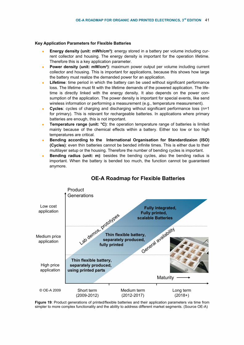
OE-A ROADMAP FOR ORGANIC AND PRINTED ELECTRONICS, 3rd EDITION 41
Key Application Parameters for Flexible Batteries
• Energy density (unit: mWh/cm³): energy stored in a battery per volume including cur-rent collector and housing. The energy density is important for the operation lifetime. Therefore this is a key application parameter.
• Power density (unit: mW/cm³): maximum power output per volume including current collector and housing. This is important for applications, because this shows how large the battery must realize the demanded power for an application.
• Lifetime: time period in which the battery can be used without significant performance loss. The lifetime must fit with the lifetime demands of the powered application. The life-time is directly linked with the energy density. It also depends on the power con-sumption of the application. The power density is important for special events, like send wireless information or performing a measurement (e.g., temperature measurement).
• Cycles: cycles of charging and discharging without significant performance loss (n=1 for primary). This is relevant for rechargeable batteries. In applications where primary batteries are enough, this is not important.
• Temperature range (unit: °C): the operation temperature range of batteries is limited mainly because of the chemical effects within a battery. Either too low or too high temperatures are critical.
• Bending according to the International Organisation for Standardizaion (ISO) (Cycles): even thin batteries cannot be bended infinite times. This is either due to their multilayer setup or the housing. Therefore the number of bending cycles is important.
• Bending radius (unit: m): besides the bending cycles, also the bending radius is important. When the battery is bended too much, the function cannot be guaranteed anymore.
Short term(2009-2012)
Medium term(2012-2017)
Long term(2018+)
ProductGenerations
OE-A Roadmap for Flexible Batteries
Thin flexible battery,separately produced,
using printed parts
Thin flexible battery,separately produced,
fully printed
Fully integrated, Fully printed,
scalable Batteries
High priceapplication
Lab demos, prototyp
es
General availability
Maturity
Medium priceapplication
Low costapplication
© OE-A 2009
Figure 19: Product generations of printed/flexible batteries and their application parameters via time from simpler to more complex functionality and the ability to address different market segments. (Source OE-A)

42 OE-A ROADMAP FOR ORGANIC AND PRINTED ELECTRONICS, 3rd EDITION
Key Technology Parameters for Flexible Batteries
• Layer thickness: the layer thicknesses of the films within a battery are critical because they directly influence the energy density and the lifetime.
• Ionic conductivity: for a high power density, a high ionic conductivity is important, on the other hand this might limit the lifetime. Therefore an optimum must be found for each application.
• Thermal stability: too low or too high temperatures are critical for batteries because of the electrochemical reactions taking place in a battery. It is important to realize a stability that is sufficient for the corresponding applications.
• Gas permeation: most battery types need an encapsulation. Here the gas penetration must be as small as possible to enable a long lifetime of the battery.
• Flexibility: for printable/organic electronics, flexibility is important in most cases. The housing of the batteries must enable this flexibility.
Red Brick Walls
• Currently flexible zinc-carbon type batteries seem to have the largest market share. But these batteries provide only a low energy density and are not rechargeable. These limits reduce the potential fields of application.
• One of the next improvement steps is the introduction of lithium technology, which is also becoming commercially available. They have several advantages, especially a high energy density. As lithium batteries count for high energy density, these batteries pro-vide longer lifetime in the application. Most of the lithium-system batteries are recharge-able this is very important for long term applications, where the battery can be re-charged by external energy, like light (by OPV) or electromagnetic field (by an antenna). On the other hand, there are also some disadvantages that need to be overcome for the realization of the next generations. Usually the production of lithium batteries has to be carried out under special atmosphere. This is a major Red Brick Wall in the moment. Special developments have to be made, for example in the encapsulation. To achieve a long lifetime the battery components have to be protected from several gases of the at-mosphere. The development of high quality barrier foils is absolute necessary in this case.
4.1.8 Smart Objects
A big advantage of organic and printed electronics is the possibility to combine and integrate multiple electronics devices to so called smart objects. These will start with some simple func-tionality, like an animated logo, and constantly grow in complexity and size, enabling large area gameboards or flexible complex systems such as smart cards. The combinations are possible due to the new materials and processes used in organic and printed electronics. This allows the integration of different devices like sensors, transistors, memories, batteries or displays onto one substrate. The integration can be realized either by one process or by a hybrid combination of several separately produced devices.
Even though, in further generations very complex systems are possible that combine a large number of single devices, the smart objects are quite simple in the beginning. The products are not as well defined as in the other application fields, therefore the roadmap does not show a continuous improvement of products for the different generations but sometimes even com-pletely different products.

OE-A ROADMAP FOR ORGANIC AND PRINTED ELECTRONICS, 3rd EDITION 43
Figure 20: Smart Card with flexible battery and electrochromic display. (Source: OE-A)
As first examples of smart objects, printed keypads, printed loudspeakers and smart cards in-corporating thin film batteries and flexible displays have been shown. In the future the trend will be towards the inclusion of more different functionalities as well as more complex functionalities, moving from simple input devices, animated logos or smart cards to objects with full displays, intelligent tickets and sensors, games, and smart packages. The variety of smart objects will be limited only by the number of available organic and printed electronic technologies and the crea-tivity of product developers. One of the key issues to look at will be taking care of mechanical and electrical compatibility and connection between the different functions.
As one of the next products on the market, animated optical features, for marketing or brand protection are expected. Other smart objects will probably be smart cards. Because of the com-plexity of the smart objects, the roadmap for these products is much harder to foresee than for the other products; on the other hand they are the products that make the full use of the possi-bilities of the printed electronics technology. In Table 14 it can be seen, that there are already first products on the market, while the next generations can have quite different functions and the development is not linear.
Key Application Parameters for Smart Objects
• Number of organic devices: the technology of printed or organic and printed electron-ics is still not in a mature state. It is therefore not simple to combine different products to a fully functional new product. The more different single devices need to be combined, the harder it will become to adjust the electrical and mechanical interfaces of the single devices.
• Complexity: like the combination of several single devices, also their complexity is an important factor that needs to be taken into account. In this case, complexity means for example number of bits of a memory, number of transistors of a circuit or sensitivity of a sensor.
• Number of uses: it will be much more easy to realize single use elements than products for multiple uses and long live. Therefore the number of uses is also a key application parameter.
• Hybrid vs. Integrated: smart objects can be realized either by an integrated or by a hybrid combination of single devices. In the long term it is probably better to integrate the devices, but especially in the beginning, a hybrid setup might be economically better and easier to realize.

44 OE-A ROADMAP FOR ORGANIC AND PRINTED ELECTRONICS, 3rd EDITION
• Shelf life: like with the number of uses, the shelf life is important, too. It is more easy to realize products for a short lifetime, while long life products have much higher demands. Therefore the shelf life, is a key application parameter, too.
Table 14: Description of the different generations of smart objects according to the actual state of technology and the major addressed markets that are expected in the medium and long term future. (Source: OE-A)
Generation Product Description Market General Availability
1 Printed ID card 16 bit ROM Tickets, game cards 2006
2 Read/Write memory card (15 bit passive) Game cards 2007
3 Animated Logo (printed display, organic circuit, battery)
Marketing, brand protection
2010
4 Smart card with printed display Smart cards 2008
5 Single use sensor (sensor, logic, battery, display)
Water quality tester 2012
6 DinA4 game board with several sensors and displays
Gaming 2014
7 Smart card with printed display, organic circuit, battery, organic sensor
Smart cards 2020
Key Technology Parameters for Smart Objects
• Available devices on mature level: as mentioned above, smart objects are only save to produce, when all the single devices used are in a technological mature state, other-wise the realization of the smart objects is very critical.
• Fit of electrical interfaces: in order to combine different electronic devices it is essential, that the electrical interfaces fit. For example a battery must have the voltage that is needed for a logical chip or a display that is integrated on the same device.
• Fit of mechanical interfaces: besides the electrical interfaces, also the mechanical connections and interfaces must fit. For example it is very hard to integrate a glass display on a flexible polymer substrate with other devices.
• Reliability: it is essential, that products work according their specifications. In smart objects, this is more critical as in other products, because of the different integrated devices, all of the single devices have variations in their properties. Typically the variations of several parameters make it less realistic for a complex system to work probably compared to a single device product.
• Lifetime: for all products lifetime is a key technology parameter. For smart objects this is even more critical due to the combination of different devices, where the device with the shortest lifetime limits the performance of the whole product.

OE-A ROADMAP FOR ORGANIC AND PRINTED ELECTRONICS, 3rd EDITION 45
Short term(2009-2012)
Medium term(2012-2017)
Long term(2018+)
ProductGenerations
OE-A Roadmap for Smart Objects
Greeting cards, animated logos
Intelligent tickets, initial smart packaging
Complex smart packaging
2-3 integrateddevices
Lab demos, prototyp
es
General availability
Maturity
3-5 integrateddevices
> 5 integrateddevices
© OE-A 2009
Figure 21: Roadmap for smart objects graphs the development of product generations over time from simpler to more complex functionality and the ability to address different market segments. (Source OE-A)
Red Brick Walls
• Availability of mature devices: the list of the key application and key technological pa-rameters gives already clear signs for the Red Brick Walls of smart objects. Even though the smart objects are very interesting products with huge potentials, it is only possible to realize combined products, when the single organic/printed devices are available in a mature status. Only this makes it possible to realize higher generations of smart objects.
• Fitting electric interfaces: the fitting of the electric interfaces is critical. Often printed/organic electronics have relatively high input demands (like supply voltage) while the output is relatively small (like voltage of a solar cell). Therefore the combina-tion can be critical, respectively only possible, when the parameters fit with each other.
• Fitting mechanical interfaces: the mechanical interfaces of the single devices must be taken into account, too. For example it is only possible to realize fully flexible systems when all the single devices are flexible. OLEDs for example are typically still based on glass substrates, this is hard to integrate together with flexible devices on polyester films.
This list of products reflects the ideas from today’s point of view. Very likely there will be changes and new kinds of products that are based on the organic and printed electronics tech-nology platforms will appear. Therefore the technology and the market in this field will continu-ously be watched and the roadmap will be updated on a regular basis.
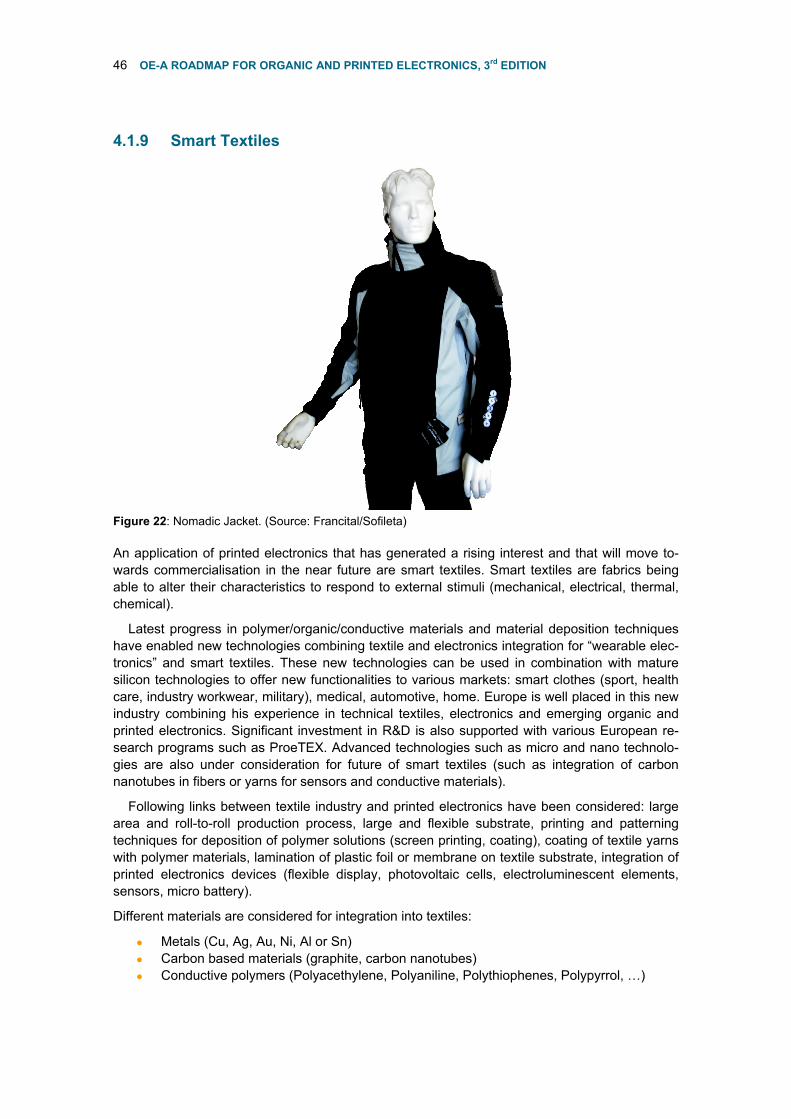
46 OE-A ROADMAP FOR ORGANIC AND PRINTED ELECTRONICS, 3rd EDITION
4.1.9 Smart Textiles
Figure 22: Nomadic Jacket. (Source: Francital/Sofileta)
An application of printed electronics that has generated a rising interest and that will move to-wards commercialisation in the near future are smart textiles. Smart textiles are fabrics being able to alter their characteristics to respond to external stimuli (mechanical, electrical, thermal, chemical).
Latest progress in polymer/organic/conductive materials and material deposition techniques have enabled new technologies combining textile and electronics integration for “wearable elec-tronics” and smart textiles. These new technologies can be used in combination with mature silicon technologies to offer new functionalities to various markets: smart clothes (sport, health care, industry workwear, military), medical, automotive, home. Europe is well placed in this new industry combining his experience in technical textiles, electronics and emerging organic and printed electronics. Significant investment in R&D is also supported with various European re-search programs such as ProeTEX. Advanced technologies such as micro and nano technolo-gies are also under consideration for future of smart textiles (such as integration of carbon nanotubes in fibers or yarns for sensors and conductive materials).
Following links between textile industry and printed electronics have been considered: large area and roll-to-roll production process, large and flexible substrate, printing and patterning techniques for deposition of polymer solutions (screen printing, coating), coating of textile yarns with polymer materials, lamination of plastic foil or membrane on textile substrate, integration of printed electronics devices (flexible display, photovoltaic cells, electroluminescent elements, sensors, micro battery).
Different materials are considered for integration into textiles:
• Metals (Cu, Ag, Au, Ni, Al or Sn) • Carbon based materials (graphite, carbon nanotubes) • Conductive polymers (Polyacethylene, Polyaniline, Polythiophenes, Polypyrrol, …)

OE-A ROADMAP FOR ORGANIC AND PRINTED ELECTRONICS, 3rd EDITION 47
Depending on the final application, these materials can be used:
• As yarns, either as such or a mix with other fibers • As a coating on synthetic or natural fibers • As conductive filler in a blend with a polymer
Table 15: Description of the different generations of smart textiles according to the actual state of technology and the major addressed markets that are expected in the medium and long term future. (Source: OE-A)
Generation Product Description Market General Availability
1 Textile input keypad for hands free communication and iPod control
Outdoor & ski jackets 2009
2 Semi flexible photovoltaic cells Computer & outdoor bags
2009
3 Heating & conductive elements Outdoor jackets 2009
4 Electroluminescent panels LED, optic fiber
Outdoor & professionnal jackets, building
2010
5 Flexible display Communication 2010
6 Monitoring sensors Medical, health care, sport
2011
7 Organic solar cells on textile Textile sensors
Professional, sport, healthcare
2014
Key Application Parameter for Smart Textiles
Application parameters are very dependent on the product usages and market. Following pa-rameters have been identified for textiles used for smart clothes.
• Washability: compatibility of material with washing powders, drying (60 °C) for textile integrated components (if not integrated, these components should be easily discon-nected). Between 20 to 50 washing cycles.
• Operational lifetime: typically 2 to 3 years. • Cost: depending on the added functionality, typically a few tens € to 100-200 € • Outline dimension: typically a few cm2 to few tens cm2. • Mechanical robustness, bending, torsion, resistance to erosion: this one of the
most critical parameters for this application, especially for connecting parts. Unlike other typical applications of printed electronics which use rigid substrates, integration into tex-tiles require materials and connecting solutions compatible with flexible substrates and able to withstand severe bending and torsion constraints.
• Power consumption: as low as possible. The source of energy is a battery which has to be as small and light as possible for wearable integration, typically lithium ion battery with output voltages 3V to 11V and output current capability of 800 mA to 1 A. The power consumption has also direct impact on the system autonomy (typically 3 to 6 hours) and time between two battery charges.

48 OE-A ROADMAP FOR ORGANIC AND PRINTED ELECTRONICS, 3rd EDITION
• Flexibility, conformability, ergonomy, easy to wear, “textile look and feel”: ideally the textile fabrics should not be altered in terms of flexibility, stretchability, breathing.
• Resistance to UV: the textile material is exposed to sun and UV rays during long pe-riod of time which may alter original material characteristics.
• Non toxicity: for material having direct contact with the skin.
Short term(2009-2012)
Medium term(2012-2017)
Long term(2018+)
ProductGenerations
OE-A Roadmap for Smart Textiles
Keypad control, textile conductive lines, Heating, LED, electroluminescent, optical fiber Hybrid Sensors (silicon)
Flexible photovoltaicsFlexible display
Flexible batteryHybrid sensors (plastic)
Organic photovoltaicsSmall power fuel cell
Fiber integrated sensorsCarbon nanotube sensors &
stretchable conductors
Lab demos, prototyp
es
General availability
Maturity
© OE-A 2009
Direct integration(e- textile fabrics)
Integration org. electronic
Hybrid Si + org. electronic
Figure 23: Roadmap for smart textiles graphs the development of product generations over time from simpler to more complex functionality and the ability to address different market segments.(Source OE-A)
Key Technology Parameters for Smart Textiles
The technology parameters are mostly related to the application parameters but not, in a simple one to one relationship. The following parameters were identified:
• Low power consumption: a few tens of mA to few hundreds mA (for heating elements application) to optimise battery size and weight and user autonomy.
• Low supply voltage: ideally 3.5V (one element lithium ion battery), 7V (two elements in series) or 11V (three elements), to use standard batteries already available for con-sumer market (cellular phones) and reduce battery size and weigth.
• Thickness: a few mm, to offer wearable integration capability. • Viscosity of fluid material (polymer, ink): for coating and screen printing on textile
substrate and compatibility with roll-to-roll industrial manufacturing process already used in the textile industry.
• Curing of fluid material: typically by evaporation by forced air flow (100 °C) in a roll-to-roll process flow.
• Low temperature process: for a given application, care must be taken to choose the right textile support, as it must not altered by the device manufacturing process. In this way, organic conductive materials open new perspectives with their low temperature process, enabling use of large range of textile materials usable as support.

OE-A ROADMAP FOR ORGANIC AND PRINTED ELECTRONICS, 3rd EDITION 49
• Operational lifetime/bias stress: typically 2 to 3 years, with 2 to 3 hours daily use (de-pending on the product and the application). Organic material may have reduced capa-bility for long operational lifetime compared to inorganic material.
Red Brick Walls
A number of potential show stoppers were discussed during the development of the roadmap. After analysis of the predicted technology development, some were found to be real potential Red Brick Walls, others appeared less critical, while additional potential issues were found. Two “Red” Brick Walls were found:
• Reliability and robustness (mechanical and washing), especially for connectors • Ergonomy for end user, including weight and volume of the battery
In addition, some “yellow” brick walls candidates were found, i.e. potential problems but possibly achievable with normal development:
• Easy to integrate for garment maker (no cables or easy interconnections) • Added cost • Development of standard functional building blocks or technology platform that could be
used as a “Lego” building block by integrators (e.g., battery, cable, display, keypads, antenna, electronics control).
4.1.10 Short List of Key Application Parameters
The viability of each application or product will depend on fulfilment of a number of parameters that describe the complexity or performance of the product (application parameters). For the applications above groups of specialists identified the most important application and technol-ogy parameters and requirements for different generations of products. Here we list only a small excerpt of the key application parameters that have been identified as relevant to several of the applications. The following list is in no particular order since the relevance of the different pa-rameters varies for the diverse applications.
• Complexity of the device: the complexity of the circuit (e.g., number of transistors) as well as the number of different devices (e.g., circuit, power supply, switch, sensor, dis-play) that are integrated have a crucial influence on reliability and production yield.
• Operating frequency of the circuit: with increasing complexity of the application (e.g., increasing memory capacity) higher switching speeds are necessary.
• Lifetime/stability/homogeneity: lifetime (shelf and operation), the environmental sta-bility, stability against other materials and solvents, and homogeneity of the materials are an issue due to the intrinsical properties of the materials.
• Operating voltage: For mobile devices powered by batteries, PV or radio frequency, it is essential to have low operating voltages (<10 V).
• Efficiency: the conversion efficiency of light to electricity or electricity to light is a key parameter for photovoltaic cells and photodiodes or OLEDs, and power efficiency of cir-cuitry is also important for many applications, especially those which are mobile and need to be light weight.
• Cost: although most applications target new applications and markets rather than re-placements, costs have to be low. For some applications, such as rollable displays, a cost premium over conventional rigid displays may be accepted, while for other applica-tions, e.g., in packaging, low cost will be a major driving factor.

50 OE-A ROADMAP FOR ORGANIC AND PRINTED ELECTRONICS, 3rd EDITION
4.2 OE-A Roadmap for Organic and Printed Electronics Applications
We have summarised the individual application roadmaps shown above into the OE-A road-map for organic and printed electronics applications seen below in Figure 24. For each of the selected applications we show products that are expected to reach the market in the short term (2009-2012), medium term (2012-2017) as well as a forecast for 2018 and beyond.
Figure 24: OE-A roadmap for organic and printed electronics applications. Forecast for the market entry in large volumes (general availability) for the different applications. The table expands and updates the second version of the OE-A roadmap (Source: OE-A).
Significant progress has been made in the last several years and the performance of the de-vices enables a first generation of products. However, in order to fulfill the specifications of fu-ture generations that are more complex, further improvement of materials, process, design and equipment is necessary.

51 OE-A ROADMAP FOR ORGANIC AND PRINTED ELECTRONICS, 3rd EDITION
5 Technology
As we have mentioned before, we use the term organic electronics for brevity to refer to the field of electronics beyond classical silicon approaches, but include concepts such as large area or flexible circuits and printed inorganic materials. Although some classic device concepts are used, materials, including substrates, and patterning processes are very different from those used in the conventional electronic industry. In this chapter the results of the roadmapping work of the technology groups on materials, processes and devices for organic are presented.
A more detailed description of the printing and other patterning processes, materials and de-vices can be found in an article in the 1st edition of the OE-A brochure, published in 2006. The brochure is available from the OE-A secretariat.
5.1 Materials
Organic electronics relies on electrically active materials that can be used as conductors, semi-conductors, luminescent, electrochromic or electrophoretic materials. The materials have to be carefully chosen since process conditions and the interplay with other layers have a large influ-ence on the performance of the device. Amongst these further layers, dielectrics and passiva-tion materials become increasingly important for the device performance.
There are many approaches on the material side and the resulting questions - organic or in-organic, solution based or evaporated - are still under discussion. It is very likely that several approaches will be used in parallel.
Organic Semiconductors are used in many active devices and many of them are solution processable and can be printed (see Figure 26). The charge transport properties largely depend on the deposition conditions like solvents, deposition technique, concentration, interfaces and so on. Most of the organic semiconductors used today are p-type (like pentacene and polythio-phene), but first n-type materials have also become available and open the door to CMOS-cir-cuits.
Figure 25: Ready to use semiconducting formulations. (Source: Merck)
The charge carrier mobility of organic semiconductors, though still much lower than crystalline silicon, has improved dramatically in recent years, already matching amorphous silicon (a-Si), and is expected to approach or match polycristalline silicon (poly-Si) in coming years, first in

52 OE-A ROADMAP FOR ORGANIC AND PRINTED ELECTRONICS, 3rd EDITION
research, where mobilities of up to 5 cm2/Vs have already been reported, and some time later in commercial products (Figure 27). This will be possible with optimized small molecule materials and polymers or new materials as e.g., inorganics, nanomaterials, carbon nanotubes or hybrid materials.
Figure 26: Structures of common materials for organic and printed electronics. a) conductor PEDOT:PSS; b) semiconductor polythiophene P3HT; c) semiconductor pentacene. (Source: OE-A)
Inorganic and small molecule organic semiconductors are of growing interest especially since deposition is no longer restricted to evaporation processes. Several semiconductors of these classes can be processed in solution or dispersion and therefore are compatible with mass printing processes. In addition, high throughput evaporation processes might enable the use of that class of materials.
Figure 27: OE-A roadmap for the charge carrier mobility of semiconductors for organic and printed electronics applications. The values refer to materials that are available in commercial quantities and to devices that are manufactured in high throughput processes. The values for amorphous silicon (a-Si) and polycrystalline silicon (poly-Si) are given for comparison. (Source: OE-A)

OE-A ROADMAP FOR ORGANIC AND PRINTED ELECTRONICS, 3rd EDITION 53
New material classes like carbon nanotubes or hybrid (organic - inorganic) material combi-nations and device architectures (like organic CMOS technologies) are further new approaches to optimize the performance of the devices.
The choice of conducting materials is strongly dependent on their application. For high metal-like conductivity it is still necessary to use filled materials like silver inks. But if conductivity is needed in combination with high transparency, e.g., for organic photovoltaics or organic LEDs, special inorganic materials like indium tin oxide (ITO) or the polymeric PEDOT:PSS represent state of the art solutions.
Transparent organic conductors are picking up in performance but still show inferior con-ductivities in comparison to metal oxides like ITO. Advantageously the polymers allow for wet processing and the flexibility of the polymer coatings makes them the chosen candidates for the replacement of brittle inorganic materials. Continued progress in increasing the electrical con-ductivity of PEDOT:PSS polymers has been achieved over the past years as evident from Figure 28. Capitalizing on its continuously improving properties, meanwhile, these materials are even qualified and used for certain sophisticated applications like touch screens and electro-chromic displays.
1998
Conductivity[S/cm2]
Conductivity of the Transparent Organic Conductors
2000 2002 2004 2006 2008 2010
1000
800
600
400
200
0
Year© OE-A 2009 Figure 28: An impressive and ongoing progress of the electrical conductivity of PEDOT:PSS-dispersions has been achieved over the past 10 years. (Source: H.C.Starck Clevios, Agfa-Gevaert)
Recently, significant progress has been made with solution based carbon nanotubes and other nano wire based concepts in terms of conductivity and transparency.
As the trend goes to fully printed devices, printable dielectrics and passivation materials will complement wet chemical processing of semiconductors.
Surface treatment and further ancillary materials might be needed to support top performance range semiconductors.

54 OE-A ROADMAP FOR ORGANIC AND PRINTED ELECTRONICS, 3rd EDITION
5.2 Substrates
A principle advantage of organic and printed electronics is that large, flexible and low cost substrates can be used. Polymer films (like polyester) are most widely used today, but paper, cardboard, thin glass and stainless steel are also prominent candidates. Special surface treatment or barrier layers can be added if necessary. The material best suited for a specific application depends on the process conditions, surface roughness, thermal expansion, and barrier properties.
As there are many different applications which are involved in flexible electronics the requirements and suitable substrate solutions can differ over a wide range.
Typical substrates are: • Thin glass • Metal foils • Paper • Polymers
o Different polyesters, especially Polyethylenterephthalate (PET) and Polyethylenenaphthalate (PEN)
o Polycarbonate (PC) homo- and copolymers o Polyimide (PI) o Polyetherimide (PEI) o Polyvinylfluorid (PVF)
The substrate basically is the playground to develop large area and/or flexible electronics. Its basic function is to be carrier which allows expanding the scope of electronics to large area sheets or rolls which can be easily handled either in batch or preferably in roll-to-roll processes. Therefore its properties need to be adapted to the processability in subsequent process steps and functionality in the application. Table 16: Substrate key technology parameters related to key application parameters. (Source: OE-A)
Key Application Parameters (some examples)
Key Technology Parameters (some examples)
Processability Mechanical properties, physical/fluidic properties, thermal properties, coating availability; outgassing, patterning possibilities (…)
Appearance Optical properties
Yield Surface properties & cleanliness (…)
Lifetime Permeability, UV stability, heat stability (…)
Scale ability Availability, material dimensions
Sustainability Recycling/environmental
Price level From low cost and low requirements (e.g., RFID antenna) to high cost and high performance (e.g., oTFT)

OE-A ROADMAP FOR ORGANIC AND PRINTED ELECTRONICS, 3rd EDITION 55
Improvements and fine tuning to the application is currently done for the mentioned properties. Each technical customization bears its own characteristic challenges and Red Brick Walls. Ba-sically all substrates are far older and well introduced in other market segments than the organic electronics market. Big production capacities do already exist worldwide in the market. There-fore in certain cases it may be more difficult to respond to a multitude of very different small volume requests in lab scale development, whereas the big volumes should be no hurdle.
Each material has its special advantages and weak points - like e.g., the smoothness and high barrier for glass substrates or the flexibility and price for paper. Plastic materials like PET, PEN or PC can be modified according to physical and surface properties over a wide range so that they can be fine tuned to serve as all-round solutions. Other plastics like PI, PEI or PVF are more specific high priced materials, which have special stability advantages against heat or weathering.
Table 17: Relative comparison of some basic properties for the different substrates. (Source: OE-A)
Generation Glass Metal Paper PET PEN PC PI PEI PVF
Smoothness ++1 ++1 0 +1 +2 +2 0 0 0
Temperature Resistance
++ ++ 0 +2 +3 0 ++ ++ ++
Flexibility -- ++ ++ ++ ++ ++ ++ ++ ++
Optical Transmittance
++ -- -- ++ ++ ++ 0 0 0
Barrier ++ +3 - +3 +5 +5 + + +
Price -- + ++ + 0 0 -- - --
1 Intrinsic property of such substrate. 2 Planarizing coatings have already been applied on these polymeric films to get Ra ≤ 1 nm. 3 Temperature resistance can be improved by extra heat stabilizing process. 4 Intrinsic high barrier of metal foils, but usually pin holes are present. 5 Barrier layers have already been applied on these polymeric films, especially subsequent organic and inorganic barrier layers can lead to very high OLED barrier quality; e.g., with WVTR = 10-6 g/m²d.
According to their specific advantages one can find the substrates in those applications, which utilize their key competitive strengths.
OLED, oTFT or photovoltaics need high barrier, smooth surface and good optical quality which for example glass or specially treated films can provide. On the other hand paper is a cheap material, where some conductive paths, EL lighting or RFID can be implemented.
Other plastics especially the polyester films grades PET and PEN offer wide range of property variations and therefore can be found in almost every application in the field of organic or large area electronics.
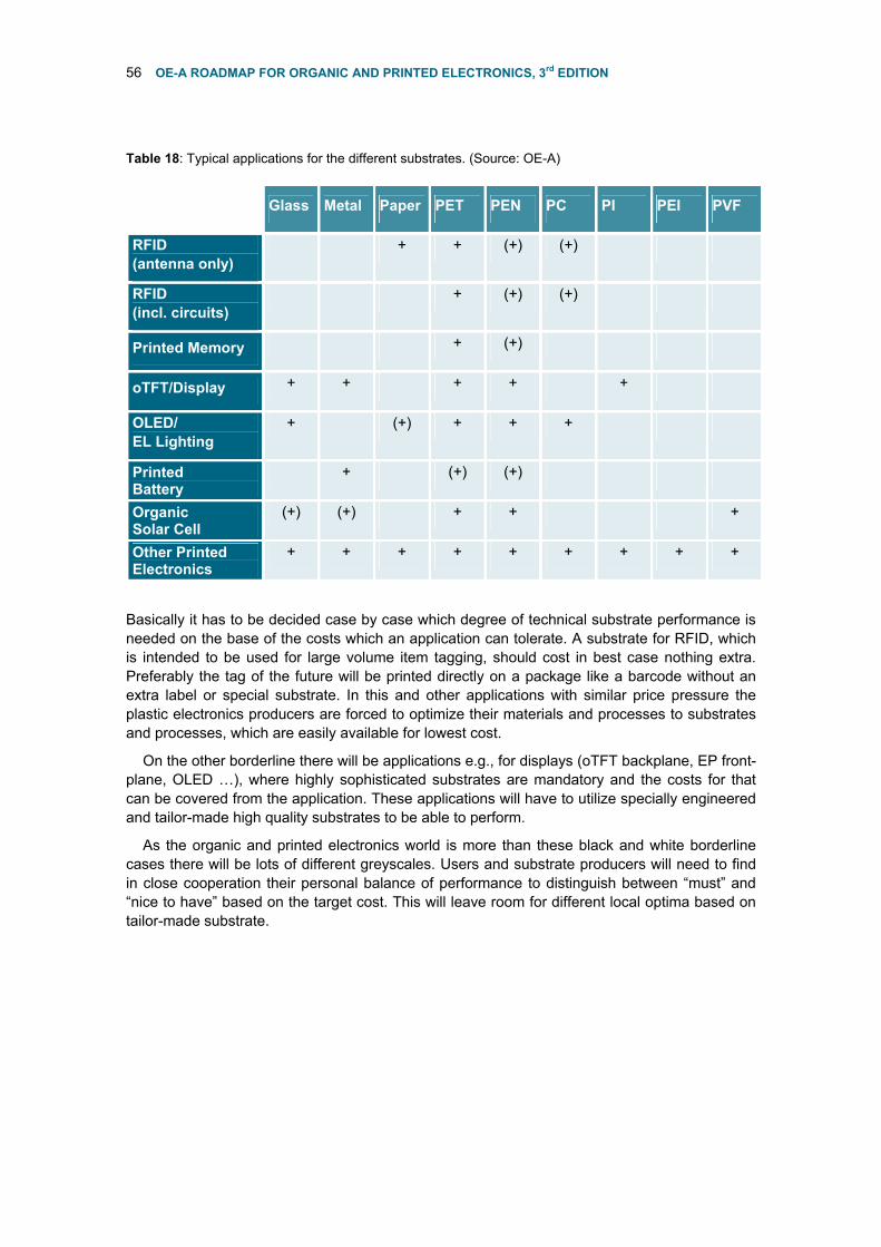
56 OE-A ROADMAP FOR ORGANIC AND PRINTED ELECTRONICS, 3rd EDITION
Table 18: Typical applications for the different substrates. (Source: OE-A)
Generation Glass Metal Paper PET PEN PC PI PEI PVF
RFID (antenna only)
+ + (+) (+)
RFID (incl. circuits)
+ (+) (+)
Printed Memory + (+)
oTFT/Display + + + + +
OLED/ EL Lighting
+ (+) + + +
Printed Battery
+ (+) (+)
Organic Solar Cell
(+) (+) + + +
Other Printed Electronics
+ + + + + + + + +
Basically it has to be decided case by case which degree of technical substrate performance is needed on the base of the costs which an application can tolerate. A substrate for RFID, which is intended to be used for large volume item tagging, should cost in best case nothing extra. Preferably the tag of the future will be printed directly on a package like a barcode without an extra label or special substrate. In this and other applications with similar price pressure the plastic electronics producers are forced to optimize their materials and processes to substrates and processes, which are easily available for lowest cost.
On the other borderline there will be applications e.g., for displays (oTFT backplane, EP front-plane, OLED …), where highly sophisticated substrates are mandatory and the costs for that can be covered from the application. These applications will have to utilize specially engineered and tailor-made high quality substrates to be able to perform.
As the organic and printed electronics world is more than these black and white borderline cases there will be lots of different greyscales. Users and substrate producers will need to find in close cooperation their personal balance of performance to distinguish between “must” and “nice to have” based on the target cost. This will leave room for different local optima based on tailor-made substrate.

OE-A ROADMAP FOR ORGANIC AND PRINTED ELECTRONICS, 3rd EDITION 57
5.3 Printing and Patterning Techniques
A wide range of large area deposition and patterning techniques can be used for organic and printed electronics. Most prominent in this context are various printing techniques that are well known from the graphic arts industry and enable reel-to-reel processing or high speed sheet to sheet processing (“mass printing methods”). However, non-contact printing methods, especially ink-jet printing, which has become widespread in the graphics industry and is seeing significant use on functional printing, are also significant, as are coating methods that do not include two dimensional patterning.
One common mass printing method that has drawn interest for functional printing is flexographic “flexo” printing. Flexo is a subset of relief printing, which also includes the very old technique of woodcuts and other stamp based printing methods. In flexo printing, as shown in Figure 29 the image to be transferred is defined as a raised area on an elastic printing form on a roll, which is usually but not always inked by transfer from an inking roll referred to as the anilox roll. By passing the substrate to be printed between the printing roll and a form cylinder, the ink on the raised areas is transferred to the substrate. Although flexo can produce very high speeds and good resolution (even below 20 µm according to recent reports on new form materials), one issue that can arise is the spreading of ink in “halos” around the edges due to the pressure on the elastic form.
Figure 29: Flexographic printing process. (Source: OE-A)
A sort of “mirror image” of flexo is gravure printing, in which the image to be transferred is defined by very small cups engraved into a printing cylinder (See Figure 30). The entire cylinder is inked, but after removal of excess with a doctor blade only the cups contain ink. The substrate is passed between the printing roller (in some laboratory scale machines plate) and impression roller and the high pressure applied together with control of surface energy causes the ink in the cups to be transferred to the substrates. An interesting aspect of gravure printing is that through control of cup size and density it is possible to transfer different amounts of material to different parts of the substrate. Through the recent advances in laser assisted and direct laser engraving the possibilities for control of material transfer and for achieving higher resolution have grown, with reports of features down to 10 µm. Gravure is popular for extremely high quality graphics printing, and has been studied intensively for functional printing as well (e.g., VTT in Finland and the EU project CONTACT).

58 OE-A ROADMAP FOR ORGANIC AND PRINTED ELECTRONICS, 3rd EDITION
Figure 30: Gravure printing process. (Source: OE-A)
Offset is one of the most common printing methods for high volume graphics printing (large sheet to sheet machines can print up to 20000 sheets, i.e. ca 15000 m2 in an hour, and roll-to-roll machines can be even faster). The term offset refers to the fact the image is not defined on the cylinder than transfers the ink to the substrate, but to an intermediate cylinder, which then transfers the image to the offset cylinder that actually transfers the ink to the substrate (see Figure 31). Typical offset involves the use of an oil-based inking solution and a water-based fountain solution, which can be highly problematic for functional polymers, but there are water-free versions as well. Offset can deliver high speed and excellent resolution but the ink require-ments (extremely high starting viscosity) are very difficult for functional materials, so that offset has not seen as much activity for printed electronics as gravure or flexo.
Figure 31: Offset printing process. (Source: OE-A)
Another very common mass printing method, well-known through its use for printing on t-shirts and the like, is screen printing (Figure 32). The image is defined through an opaque mask, which is applied to a fine mesh material. The ink is spread over the screen with a doctor blade

OE-A ROADMAP FOR ORGANIC AND PRINTED ELECTRONICS, 3rd EDITION 59
and transferred to the substrate by applying pressure to the screen with an elastic squeegee, which forces the ink through the screen in the non-masked areas onto the substrate, ideally without direct contact between screen and substrate. Screen printing can not in general deliver quite the speeds or resolution of flexo, gravure and offset but is very suitable when relatively thick films are needed, and through rotary screen printing significant volume can be achieved. Screen printing is used extensively in printed circuit board (PCB) manufacturing.
Figure 32: Screen printing process. (Source: OE-A)
Ink-jet printing is well known through the proliferation of low-cost office color ink-jet printers but has also been one of the most popular methods for investigating printing of functional materials. In this method, very small droplets of ink are ejected from print heads onto the substrate through thermal or piezoelectric effects (Figure 33). The resolution achievable is dependent on the amount of ink ejected (down to 1 pl has been achieved), the control of droplet spreading (print head and ink optimization) and the surface energy control of the substrate, but features on the order of a few µm have been achieved. In contrast to the previously described mass printing methods, ink-jet is completely digital, which means that each substrate can in principle be printed differently. This opens up possibilities for large productions runs of individually defined unique products and for correction of distortion effects in multi-step processes. Furthermore, the low viscosity required for ink-jet printing is sometimes easier to achieve with functional materials. On the other hand, equipment costs can be higher and throughput lower than with mass printing technologies.
Figure 33: Ink-jet deposition mechanism (piezo). (Source: OE-A)

60 OE-A ROADMAP FOR ORGANIC AND PRINTED ELECTRONICS, 3rd EDITION
Registration accuracy, i.e. how well the patterns in successive printed layers are aligned with each other, is a further critical parameter for printing electronic circuits, where misalignment can lead to complete circuit malfunction. Commercial multi-stage mass printing machines for the graphics industry have registration accuracies in a wide range from about 30 µm (or better) to 200 µm and even more. For paper substrates and sheet processes the registration is typically better than for plastic film substrates and roll-to-roll processes. In high quality machines one can have in-line registration accuracies on the order of 10 µm or less with added cost in sheet to sheet and fully in-line roll-to-roll mode. However, these values are purely machine values and say nothing about substrate distortion, which will happen through handling, printing and curing processes in almost any free-standing flexible substrate. This distortion can partially but not completely be compensated by accounting for reproducible distortion in the layout for succes-sive layers. This could become a significant issue for small critical dimensions on large sub-strates or wide webs. Digital printing processes such as ink-jet printing, on the other hand, can, in conjunction with the right imaging systems, perform in-line distortion correction over very large areas; this comes however at the cost of lower throughput.
Table 19 summarizes some of the key parameters of common printing techniques, such as resolution, speed, film thickness and viscosity requirements. In most cases, a final product will almost certainly require a mixture of printing methods. In general, the viscosity requirements for mass printing processes pose a challenge for functional materials, since the common approach in the printing industry of adding binders generally effects the functional quality of the material negatively and other approaches need to be taken. However, good performance of organic semiconductors deposited by mass printed has been reported recently.
Table 19: Some basic parameters of common printing technologies. (Source: Bruce Kahn, Printed Electrionics Consulting, “Organic Electronics Technology”, VDMA, 2006; Gerhard Klink, Fraunhofer IZM, “Abschlussbericht zum Projekt PropolyTec”, 2006)
Printing Method Speed (m/min) Resolution (µm) Film Thickness (µm) Viscosity (Pas)
Flexo 50-80 20-50 0.5-2 0.05-0.5
Gravure 20-100 20-50 0.5-2 0.05-0.2
Offset 15-100 15 0.5-2 30-100
Screen 10-100 80-100 5-25 0.5-50
Ink-jet n.a. 20 100-500 0.002-0.025
In addition to the relatively established processes described above, novel patterning techniques such as laser ablation, large area vacuum deposition, soft lithography and large area optical lithography also offer promise for application in organic and printed electronics but will not be discussed in detail here. Each method has its individual strengths, and in general, processes with a higher resolution have a smaller throughput, as shown graphically below in Figure 34.
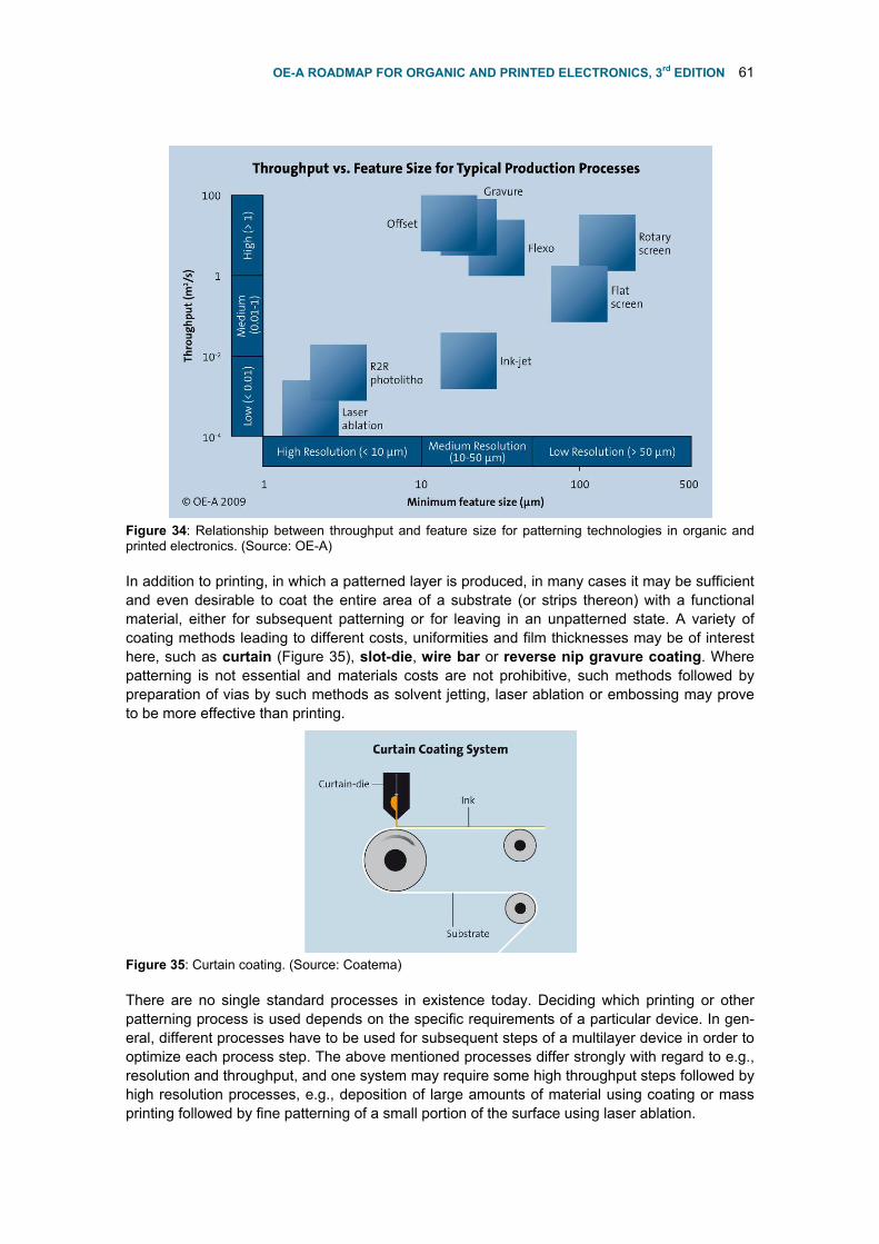
OE-A ROADMAP FOR ORGANIC AND PRINTED ELECTRONICS, 3rd EDITION 61
Figure 34: Relationship between throughput and feature size for patterning technologies in organic and printed electronics. (Source: OE-A)
In addition to printing, in which a patterned layer is produced, in many cases it may be sufficient and even desirable to coat the entire area of a substrate (or strips thereon) with a functional material, either for subsequent patterning or for leaving in an unpatterned state. A variety of coating methods leading to different costs, uniformities and film thicknesses may be of interest here, such as curtain (Figure 35), slot-die, wire bar or reverse nip gravure coating. Where patterning is not essential and materials costs are not prohibitive, such methods followed by preparation of vias by such methods as solvent jetting, laser ablation or embossing may prove to be more effective than printing.
Figure 35: Curtain coating. (Source: Coatema)
There are no single standard processes in existence today. Deciding which printing or other patterning process is used depends on the specific requirements of a particular device. In gen-eral, different processes have to be used for subsequent steps of a multilayer device in order to optimize each process step. The above mentioned processes differ strongly with regard to e.g., resolution and throughput, and one system may require some high throughput steps followed by high resolution processes, e.g., deposition of large amounts of material using coating or mass printing followed by fine patterning of a small portion of the surface using laser ablation.

62 OE-A ROADMAP FOR ORGANIC AND PRINTED ELECTRONICS, 3rd EDITION
5.4 Devices
The organic materials can be combined to a number of active components such as transistors, diodes, various types of sensors, memories, photovoltaic cells, displays or batteries. Examples for passive devices are conductive traces, antennas, resistors, capacitors or inductors.
Transistors are a key component of many electronic devices, including RFID or oTFT back-planes for displays, and are a building block for most electrical circuits. An example of the con-figuration of a typical organic field-effect transistor is shown in Figure 36. Essentially, the device consists of four layers: gate electrode, insulator, source/drain electrodes and the semiconductor. The current flow between source and drain electrode is switched, depending on the voltage applied at the gate electrode. In order to optimize the transistor properties, the channel length should be as small as possible and the mobility of the organic semiconductor should be as high as possible.
Figure 36: Typical oFET (organic field-effect transistor) configuration and connections. The thickness of the layer stack is typically below 1 µm. (Source: OE-A)
The other key active components in organic and printed electronics are diodes. These can be large-area devices such as OLEDs based on small molecules or polymers (Figure 37) or photovoltaic cells (Figure 38), or small area components in a circuit. In particular, rectifying diodes are a key component in RF circuits and recently have been demonstrated in display backplanes and memory cells as well. Typically a diode consists of two electrodes (one of them transparent for photovoltaic cells or OLEDs) and anywhere between one and several organic layers with different functions such as hole or electron transport, light absorption or light emission. OLEDs and photovoltaic cells can be seen as mirror images of each other: whereas OLEDs convert electricity into light, PV cells convert light into electricity.

OE-A ROADMAP FOR ORGANIC AND PRINTED ELECTRONICS, 3rd EDITION 63
Figure 37: Typical configuration for a polymer based OLED. Small molecule OLEDs may have a number of layers with different functions. The thickness of the layer stack is typically below 1 µm. (Source: OE-A)
Figure 38: Typical configuration for an organic photovoltaic cell. The thickness of the layer stack is typically below 1 μm. (Source: OE-A)
Capacitors can, in addition to their use in electronic circuits, have specific functionality as well. For example, EL (electroluminescent) foils are a kind of capacitor consisting of a film of pigment particles, usually based on zinc sulfide (ZnS), between electrodes. When alternating current is passed through the film electrons in the ZnS are accelerated and excite the material, causing it to emit light.

64 OE-A ROADMAP FOR ORGANIC AND PRINTED ELECTRONICS, 3rd EDITION
5.5 Technology Levels
The technologies that are used in organic and printed electronics range from batch, clean-room, etching based processes to mass printing processes that are capable of deposition of square meters of substrates per second.
Here is a rough classification of the technologies in three different technology levels:
• The wafer level technology includes batch processing, typically film substrates on a carrier. An adapted semiconductor line is used for processing. High resolution can be achieved by vacuum deposition and/or spin coating followed by photolithography and wet or dry etching. The production cost is relatively high and the process is not com-patible for conversion to in-line sheet to sheet or reel-to-reel processes.
• Under hybrid technologies, we summarize combinations of processes including large area photolithography, screen printing or PCB technologies that make use of flexible substrates (e.g., polymer films or paper). Deposition of materials is by spin coating, doc-tor blading or large area vacuum deposition, in some cases also partly by printing. Ink-jet printing and laser-patterning are further technologies that are grouped in the hybrids and enable production at a medium cost level.
• Fully printed means continuous, automated mass-production compatible printing and coating techniques (flexo, gravure, offset, slot-die etc.), flexible substrates and reel-to-reel technology (Figure 39). Although all-printed devices do not yet show as high resolu-tion or performance as those made using wafer or hybrid processes, mass printing has great potential for very low cost production and will be able to deliver extremely large numbers of products. At the same time it requires significant volumes of materials even for trials, and will need large volume applications to properly utilise such high-throughput equipment.
Figure 39: Reel-to-reel processing. (Source: Acreo)

OE-A ROADMAP FOR ORGANIC AND PRINTED ELECTRONICS, 3rd EDITION 65
5.6 Short List of Key Technology Parameters
The detailed application parameter specifications for the different applications and product gen-erations help define the requirements that have to be fulfilled from technology side. The tech-nology parameters are more “fundamental” and describe fundamental material, device or proc-ess properties. As with the application parameters, we only list a small excerpt of the key tech-nology parameters identified for the various applications, focussing on those that are relevant to a number of applications.
• Mobility/electrical performance (threshold voltage, on/off current): the performance (operating frequency, current driving capacity) of the circuits depends on the carrier mobility of the semiconductor, the conductivity of the conductor and the dielectrical be-haviour of the dielectric materials.
• Resolution/registration: the performance (operating frequency, current driving capac-ity) and reliability of the circuits depends on the lateral distance of the electrodes (reso-lution) within the devices (e.g., transistors) and the overlay accuracy (registration) be-tween different patterned layers.
• Barrier properties/environmental stability: the lifetime depends on a combination of the sensitivity of the materials and devices to oxygen and moisture and the barrier properties of protective layers, substrates and sealants against oxygen and moisture. The necessary barrier properties vary for the different applications over several orders of magnitude.
• Flexibility/bending radius: thin form factors and flexibility of the devices are key ad-vantages of organic and printed electronics. In order to achieve reliable flexibility and even rollable devices materials, design and process have to be chosen carefully.
• Fit of process parameters (speed, temperature, solvents, ambient conditions, vacuum, inert gas atmosphere): in order to have a sufficient working system, it is im-portant to adjust the parameters of the different materials and devices used to build or-ganic and printed electronics.
• Yield: low cost electronics in high volumes are only possible when the processes allow production at high yields. This includes safe processes, adjusted materials and circuit designs as well as an in-line quality control.

66 OE-A ROADMAP FOR ORGANIC AND PRINTED ELECTRONICS, 3rd EDITION
6 Principle Challenges
One goal of the roadmap is to identify Red Brick Walls - principle challenges that can only be overcome by major breakthroughs beyond the expectations of standard technology develop-ment. For each application the requirements for product generations were compared with ex-pected technology development and the key challenges were identified and discussed. Like the key application and key technology parameters, the Red Brick Walls may vary for the different applications. Those discussed below are valid for all applications and summarise the most im-portant ones.
A common feature of all future generations of the different products is that the complexity and overall size of logic circuits is increasing. In certain cases, the applications include mil-lions of transistors, other combine various different electronic devices like circuit, power supply, sensors, displays and switches. In the future more and more higher and higher performance components will have to be fit into smaller and smaller areas, which for other applications high performance components will have to be placed precisely over large areas, up to a few square meters. At the same time, wafer level processing will not in the long term be a commercially viable approach for a number of applications and hybrid or fully printed processes will need to be used.
Based on the above considerations and the results of the work of the application and tech-nology groups, we believe that major breakthroughs in the following areas are absolutely nec-essary:
• Resolution, registration and process stability of the patterning processes • Charge carrier mobility and electrical conductivity of the semiconductor and
conducting materials • Circuit design including CMOS-transistors
These challenges cannot be treated in separate ways since they depend on each other. Reso-lution and registration accuracy differ for the various patterning techniques and even within a technique largely depend on the throughput or printing speed. The process stability depends on tolerable deviation, the circuit design and the materials that are used.
In order to enable mass production of complex devices, resolution better than 10 µm with as good or better registration accuracy, even on plastic substrates, is necessary. This cannot be achieved with the current level of development in high throughput, large area processes. At the same time, new strategies for the quality control enabling high speed in-line measurement and electrical testing have to be developed. These developments will be essential to enabling low cost production at high volumes and yield.
Charge carrier mobility over 1 cm2/Vs at minimum for processable semiconductors will be needed. These values have to be achieved in the final device using high volume processes. Charge carrier mobility in the order of 5-10 cm2/Vs in printable commercially available materials would represent a breakthrough since would enable more complex devices. Further optimisation of existing materials or development of novel classes of materials will be needed to achieve this. In addition to polymers, potential candidates include small molecule and inorganic semicon-ductor materials as well as nanomaterials and new hybrid systems that can be processed from solution.
Another principle challenge is the circuit design for complex circuits that are compatible with a broad range of materials and mass printing processes. In particular, CMOS type circuits need to be developed, which requires high quality p- and n-type semiconductors. This will enable

OE-A ROADMAP FOR ORGANIC AND PRINTED ELECTRONICS, 3rd EDITION 67
complex circuit designs and will significantly increase functionality of the devices, as it did previ-ously in silicon technology. CMOS design also brings significant advantages in yield and power consumption. In addition, designs for lower supply voltages and higher frequencies are of great importance.
A key reason to identify Red Brick Walls is to help the organic and printed electronics com-munity align its efforts to solve the most pressing problems. Long-term strategies, funding and new partnerships along the value chain are necessary to overcome the Red Brick Walls.

68 OE-A ROADMAP FOR ORGANIC AND PRINTED ELECTRONICS, 3rd EDITION
7 Summary and Outlook
Organic and printed electronics is a new and fascinating platform technology that enables fresh electronic applications in many fields, such as interactive toys, RFID-tags, sensors, rollable displays or flexible solar cells, which are now entering the market. With this third version of the OE-A roadmap, we have updated and expanded the information about our view of the develop-ments in this field. We included new applications, updated the status, key parameters and ex-pected technology development for them and used this updated information to identify the key challenges, which we call Red Brick Walls. We have also tried to bring the basic information together to a relatively simple picture of the main developments in this field from the application and technology point of view.
We have found that the technology is mature enough to enter the market with first, relatively simple products, addressing interesting market segments, and since the last edition of the road-map new products have started to appear. We also have seen that mass markets could be reached in the near future but will depend on progress in the fields of material, equipment, proc-esses and device design. Some of this progress will be straightforward, while we have identified some areas where breakthroughs will be needed.
For example, the development of an organic CMOS-like technology could result in a break-through of organic and printed electronics, just like it did with silicon electronics. Improved pat-terning processes and materials with better electrical performance and processability are key for future product generations. It is expected that new organic and inorganic materials will play an important role.
Also important are the new developments in in-line quality control of electrical parameters, especially in printing processes. This will allow sufficiently high yields to reach low cost, high volume products. Standardization in materials, processes and device design gain more and more importance as organic and printed electronics is entering the production phase.
However, some questions remain open; for example we have not yet been able to define a simple “Moore’s law” for organic and printed electronics or identify the “killer application” in the long term. Organic and printed electronics is still a very young field, and there are still many different parameters that are important for the further success of organic and printed electronics; it is not clear which of these might have the most important role or how they will scale. However, there are indications that such parameters as charge carrier mobility, feature size and circuit complexity could become candidates for simple scaling laws in the future. We also have not yet been able to identify the “killer application” for organic and printed electronics in the long term; there are many fascinating applications and time will tell which of these - or new ones we have not yet thought of - will turn into a “killer application”.
Organic and printed electronics is now in the market and has great potential for further growth.
We will continue to follow the developments to find the major trends, and present an updated roadmap every two years. The organic and printed electronics roadmap is an ongoing task and key activity of the OE-A and its members.
Organic and Printed Electronics is a disruptive technology that will create a wealth of new products that we cannot even think of today. OE-A will keep you updated.

OE-A ROADMAP FOR ORGANIC AND PRINTED ELECTRONICS, 3rd EDITION 69
Note The full version of the roadmap is available for OE-A members and includes detailed tables for the key application and technology parameters as well as tables for functional materials, substrates, and printing and patterning techniques in the Annex.

70 OE-A ROADMAP FOR ORGANIC AND PRINTED ELECTRONICS, 3rd EDITION
8 Acknowledgements
This roadmap was a group effort. Our thanks go to working group spokespersons and their teams, as well as the numerous members of OE-A who contributed through discussions at working groups meetings.
Application Working Groups
Organic Photovoltaic Spokesperson: Christoph Brabec, Konarka Technologies/University Erlangen; Team: Markus Scharber, Konarka Technologies; Mary Boone, Plextronics; James Dietz, Plextronics; Vishal Shrotriya, Solarmer Energy; Bill A. MacDonald, DuPont Teijin Films, Dario Della Sala, ENEA
Flexible Display Spokesperson: Donald Lupo, Technology Consulting; Team: Yong-Young Noh, ETRI; Sébastien Sanaur, EMSE; David N. Liu, Vivien Hsieh, Jessie Lin, Rachel Huang, ITRI; Gerwin Gelinck, Holst Centre; Ahila Krihnamoorthy, Honeywell Electronics Materials; Mark Goulding, Merck; Albert van Breemen, ASML
OLED/EL Lighting Spokespersons: Karl Leo, TU Dresden IAPP; Noel Clarke, Novaled; Team: Judith Ihle, Schreiner Group; Christine Boeffel, Fraunhofer IAP; Wilfried Hedderich, BAYER MaterialScience
Printed RFID Spokesperson: Wolfgang Clemens, PolyIC; Team: Peter Eckerle, BASF Future Business; Dario Della Sala, ENEA
Printed Memory Spokesperson: Per Bröms, Thin Film Electronics; Team: Wolfgang Clemens, PolyIC; Werner Zapka, Xaar Jet
Organic Sensor Spokesperson: Tony Killard, DCU-NCSR; Team: Marc Koetse, Holst Centre; Gerhard Klink, Fraunhofer IZM; Dario Della Sala, ENEA; Herman Schoo, Holst Centre
Flexible Battery Spokesperson: Martin Krebs, VARTA Microbattery, Team: Bertrand Fillon, CEA; Lars-Olov Hennerdal, Acreo; Gunter Hübner, Hochschule der Medien Stuttgart; Reinhard Baumann, TU Chemnitz; Andreas Tanda, plastic electronics
Smart Objects Spokesperson: Wolfgang Clemens, PolyIC, Team: Arved Hübler, TU Chemnitz, Tony Killard, DCU-NCSR; Dirk Kähler, Fraunhofer ISIT; Peter Dyreklev, Thin Film Electronics; Carsten J. Winnewisser, CSEM
Smart Textiles Spokesperson: Laurent Jamet, Sofileta, Team: Nicolas Renaud Cetemmsa; Isabelle Chartier, CEA

OE-A ROADMAP FOR ORGANIC AND PRINTED ELECTRONICS, 3rd EDITION 71
Technology Working Groups
Materials Spokesperson: Michael Heckmeier, Merck; Team: Johannes Canisius, Merck; Timo Meyer-Friedrichsen, H.C. Starck Clevios; Dirk Bollen, Agfa-Gevaert; Jürgen Steiger, Evonik; Peter Eckerle, BASF Future Business; Mary Boone, Plextronics; Jasmin Wörle, PolyIC; Detlef Gaiser, H.C. Starck Clevios; Mark Abendroth, ELANTAS Beck
Substrates Spokesperson: Oliver Klein, Mitsubishi Polyester Film, Team: Wolfgang Schmidt, Felix Schoeller; Julia Hitzbleck, BAYER MaterialScience; Keith Rollins, DuPont Teijin Films; Edgar Habich, Papierfabriken Cham Tenero, Peter T.M. Giesen, Holst Centre; Jani-Mikael Kuusisto, VTT
Patterning Processes Spokesperson: Gerhard Klink, Fraunhofer IZM; Team: Karlheinz Bock, Fraunhofer IZM; Sheldon Stoute M-solve, Donald Lupo, Technology Consulting
In addition numerous representatives from OE-A Member companies contributed through discussions at working groups meetings.
OE-A Members Total 129 (as of 02.12.2009)
Companies
ACT Advanced Connection Techn. Inc. (TW) ASC (DE) Agfa Gevaert N.V. (BE) ALTANA AG (DE) Applied Laser Engineering Ltd. (GB) ASML Netherlands B.V. (NL) Balluff GmbH (DE) BASF Future Business GmbH (DE) Bayer Materialscience AG (DE) Werner Blase GmbH & Co. KG (DE) Robert Bosch GmbH (DE) Botest System GmbH (DE) Brückner Maschinenbau GmbH & Co KG (DE) Bundesdruckerei GmbH (DE) Robert Bürkle GmbH (DE) Coatema Coating Machinery GmbH (DE) Coherent GmbH (DE) COPACO GmbH & Co. KG (DE) DLR, PT (DE) DuPont Teijin Films (UK) Dynacc GmbH (DE) ELANTAS Beck GmbH (DE) Evonik Degussa GmbH (DE) Felix Böttcher GmbH & Co. KG (DE) Felix Schoeller Service GmbH & Co. KG (DE) Fujifilm Dimatix Inc. (US) Fusion UV Systems GmbH (DE)
GRT GmbH & Co. KG (DE) GSI Technologies (US) H.C. Starck Clevios GmbH (DE) Honeywell Electronic Materials (US) IDAM - INA Drives & Mechatronics GmbH (DE) In-Core Systèmes (FR) INFINISCALE (FR) iTi - Imaging Technology Int. Ltd. (US) ISOVOLTA AG (AT) ISRA SURFACE VISION GmbH (DE) Werner Kammann Maschinenfabrik GmbH & Co.KG (DE) Konarka Technologies Inc. (US) KSG Leiterplatten GmbH (DE) Leonhard Kurz Stiftung & Co. KG (DE) manroland AG (DE) Mekoprint A/S (DK) Merck KGaA (DE) Mitsubishi Polyester Film GmbH (DE) M-SOLV Ltd. (GB) Mühlbauer, Inc. (US) Norrköping Science Park (SE) Novaled AG (DE) NTERA Ltd. (IE) OrganicID (US) Ormecon GmbH (DE) Papierfabriken Cham-Tenero AG (CH) PCAS - SJPC (CA)

72 OE-A ROADMAP FOR ORGANIC AND PRINTED ELECTRONICS, 3rd EDITION
plastic electronic GmbH (AT) Plextronics Inc. (US) Polyera Corp. (US) PolyIC GmbH & Co. KG (DE) Printcolor Deutschland GmbH (DE) Printed Electronics Ltd. (UK) Reinhausen Plasma GmbH (DE) Rieke Metals Inc. (US) S1 Optics GmbH/IST Metz (DE) Samsung Deutschland GmbH (DE) Schneider Electric Industries (FR) Schneidler Elektronik AB (SE) Schreiner Group GmbH & Co. KG (DE) Schweizer Electronic AG (DE) Sofileta SA (FR) Solarmer Energy Inc. (US) Solvay S.A. (BE) Technology Consulting (DE) tesa SE (DE) Thin Film Electronics (SE) Toray Plastics Europe (FR) TYCO Electronics AMP GmbH (DE) VARTA Microbattery GmbH (DE) VDI/VDE/IT (DE) Xaar plc (GB) Universities/Institutes Acreo AB (SE) Aristotle University of Thessaloniki (GR) Carnegie Mellon University (US) CEA (FR) Center f. Organic Photonics and Electronics - COPE (US) Centre for Process Innovation (GB) Centre Technique du Papier (FR) Cetemmsa (ES) CSEM (CH) CSIRO (AU) EMSE, Gardanne (FR) ENEA (IT) Energy Research Centre of the Netherlands - ECN (NL) ETRI (KR) Hochschule für angewandte Wissenschaften - FH München (DE) Fontys University of Applied Sciences (NL) Fraunhofer Alliance POLO (DE) Fraunhofer IAP (DE) Fraunhofer ILT (DE) Fraunhofer IPA (DE) Fraunhofer IPMS (DE) Fraunhofer ISC (DE) Fraunhofer ISE (DE) Fraunhofer ISIT (DE) Fraunhofer IZM (DE) Ghent University (BE) Hochschule der Medien IAF, IAD (DE) Holst Centre (NL) HSG-IMIT (DE) Industrial Technology Research Institute (TW)
InnovationLab GmbH (DE) Instytut Technologii Elektronowej (PL) Joanneum Research (AT) Konkuk University FDRC (KR) LIOS, University Linz (AT) National Centre for Sensor Research (IE) Photonics Research Institute AIST (JP) Royal College of Art (UK) Sunchon National University (KR) Tampere University of Technology (FI) Technical University Chemnitz, pmTUC (DE) Technische Universität Darmstadt, IDD (DE) Technical University Dresden, IAPP (DE) Technische Universität Hamburg Harburg (DE) TEI - Technological Educational Institutions of Athens (GR) Universitat Autònoma de Barcelona - Cephis (ES) University of California, Los Angeles (US) University of Manchester (GB) University of Leeds - Digital Print CIC (GB) VTT (FI)

OE-A ROADMAP FOR ORGANIC AND PRINTED ELECTRONICS, 3rd EDITION 73
9 Imprint
Editors Wolfgang Clemens, PolyIC GmbH & Co. KG Donald Lupo, Technology Consulting Klaus Hecker, VDMA/OE-A Sven Breitung, VDMA/OE-A Publisher Organic Electronics Association (OE-A) A Working Group within VDMA e.V. Lyoner Straße 18 60528 Frankfurt am Main, Germany E-Mail [email protected] Internet: www.vdma.org/oe-a Contact Headquarter, Frankfurt am Main, Germany Dr. Klaus Hecker Managing Director Phone +49 69 66 03-13 36 E-Mail [email protected] North American Office, Pittsburgh PA, USA Barbara Fisher Regional Manger Phone +1 412 828 0370 E-Mail [email protected] Copyright 2009 Organic Electronics Association A Working Group within VDMA e.V.
Picture Sources Cover picture Gérard Boissinot, Fotolia Pictures in Figure 1 and Figure 24: Organic Photovoltaic, Schott Solar AG Flexible Display, Plastic Logic Ltd. OLED/EL Lighting, Novaled AG Printed RFID, PolyIC GmbH & Co. KG Printed Memory, Thin Film Electronics AB Organic Sensor, Fraunhofer IZM Flexible Battery, VARTA Microbattery GmbH Smart Objects, Holst Centre Smart Textiles, Francital Environnement
Figure 4: Konarka Technologies, Inc. Figure 8: Plastic Logic Ltd. Figure 11: Novaled AG Figure 13: PolyIC GmbH & Co. KG Figure 15: Thin Film Electronics AB Figure 17: Fraunhofer IZM Figure 19: VARTA Microbattery GmbH Figure 21: Holst Centre Figure 23: Francital Environnement

Organic Electronics Association (OE-A)
A working group within VDMA
Lyoner Strasse 18
60528 Frankfurt
Germany
Phone +49 69 6603-1336
Fax +49 69 6603-2336
E-Mail [email protected]
Internet www.oe-a.org
www.oe-a.org