which one is better? comparing options to describe
TRANSCRIPT

DesignCon 2013
Which one is better? Comparing
Options to Describe Frequency
Dependent Losses
Dr. Eric Bogatin, Bogatin Enterprises
Dr. Don DeGroot, CCN & Andrews University
Dr. Paul G. Huray
Dr. Yuriy Shlepnev
2
Abstract In any channel operating at 2 Gbps and above, conductor and dielectric losses can
dominate channel performance. These effects must be included in any accurate system
simulation. The problem isn’t that simulators don’t do this; there are several choices in
interconnect loss mathematical expressions and it’s difficult to decide how to transform
fab information into simulator input.
There are different combinations of parameterized mathematical expressions for
dielectric and conductor loss which are in popular use in the industry. Each works to
some extent. This paper takes each mathematical expression, explains its origin, evaluates
its predicted insertion loss magnitude and phase then explores how the expression scales.
This is useful when translating test coupon results into accurate simulation predictions.
Author(s) Biography
Dr. Eric Bogatin received his BS in physics from MIT and MS and PhD in physics from
the University of Arizona in Tucson. He has held senior engineering and management
positions at Bell Labs, Raychem, Sun Microsystems, Ansoft and Interconnect Devices.
Eric has written 6 books on signal integrity and interconnect design and over 300 papers.
His latest book, Signal and Power Integrity- Simplified, was published in 2009 by
Prentice Hall. He is currently a signal integrity evangelist with Bogatin Enterprises, a
wholly owned subsidiary of Teledyne LeCroy. He is also an Adjunct Associate Professor
in the ECEE department of University of Colorado, Boulder. Many of his papers and
columns are posted on the www.beTheSignal.com web site.
Dr. Don DeGroot operates CCN (www.ccnlabs.com), a test and design verification
business he co-founded in 2005 to support high-speed electronic design. Don has over 25
years experience in high-frequency electrical measurements and design, including his
PhD degree from Northwestern University and 12 year of research at NIST. Don
currently focuses on interconnection and PCB material characterization for serial data
applications.
Dr. Paul G. Huray is Professor of Electrical Engineering at the University of South
Carolina and has worked at the Oak Ridge National Laboratory, Intel, and the White
House. Huray introduced the first graduate program on signal integrity and is the author
of Maxwell’s Equations and The Foundations of Signal Integrity.

3
Dr. Yuriy Shlepnev is President and Founder of Simberian Inc., where he develops
Simbeor electromagnetic signal integrity software. He received M.S. degree in radio
engineering from Novosibirsk State Technical University in 1983, and the Ph.D. degree
in computational electromagnetics from Siberian State University of Telecommunications
and Informatics in 1990. He was principal developer of electromagnetic simulator for
Eagleware Corporation and leading developer of electromagnetic software for simulation
of signal and power distribution networks at Mentor Graphics. The results of his research
are published in multiple papers and conference proceedings.

4
Introduction In any channel operating at 2 Gbps and above, conductor and dielectric losses can
dominate channel performance. Conductor loss is dominated by the resistive losses from
the current redistribution related to skin depth effects and the impact of surface texture on
one or all copper surfaces increasing the loss due to absorption of the propagating
electromagnetic field.
The dielectric loss is dominated by the material properties described by the dissipation
factor and dielectric constant of the laminates, and their relative distribution in the stack
up.
Both mechanisms contribute to frequency dependent loss and to dispersion in the speed
of the signal. The dispersion can be easily described by an effective dielectric constant.
These mechanisms must be included in any accurate system simulation. The problem
isn’t that simulators don’t do this; there are several choices for interconnect loss
mathematical expressions. While it is often possible to get accurate information about the
cross section geometry information, it is a challenge to get material properties
information in a format that immediately translates into mathematical parameters and
results in accurate simulation.
A number of studies [1], [2], [3] have reported success in fitting parameterized
mathematical expressions for loss to specific measured test lines. There is no guarantee
that measured data in a high volume manufacturing environment will be R&D laboratory
quality. With noise added, while a good match may be obtained, there may not be a
unique solution.
Rather than take specific measurements and fit parameters of a model, in this study each
of the popular mathematical expressions are evaluated to compare the sensitivity of their
parameters to the predicted frequency dependence of loss and dispersion.
A few examples are offered for how to fit parameters to measured data.
Mathematical Expressions for interconnect loss Any real interconnect will have a causal performance. The most valuable mathematical
expressions that are the basis of simulating insertion loss in transmission lines should be
causal.
To first order the conductor and dielectric losses are independent. This may not always be
a good assumption. There may be some connection between the tooth structure of the
copper surface texture and the dielectric material, changing the effective Dk or Df of the
laminate. [4], [5] In this study, we assume the two mechanisms are independent.
Conductor Texture Power Loss Mechanisms:
5
There are four popular mathematical expressions [6] used to describe conductor power
loss:
1. A smooth copper-skin depth based power loss [7].
2. The Hammerstad empirical fit for surface texture which includes dependence on
an rms deviation term.
3. A modified Hammerstad empirical fit for surface texture which includes an
additional surface area factor and an rms deviation term.
4. The Huray snowball model [8] for surface texture which models the surface as a
collection of copper spherical balls electrodeposited on a Matte or Flat base
copper surface. This model is independent of rms deviation.
In each mathematical expression, the macroscopic parameters which define the base
conductor cross section and material properties are the same:
Line width, w
Conductor thickness, t
Bulk conductivity, σ
They differ in their description of copper surface texture.
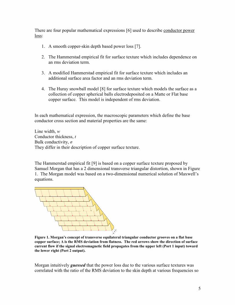
The Hammerstad empirical fit [9] is based on a copper surface texture proposed by
Samuel Morgan that has a 2 dimensional transverse triangular distortion, shown in Figure
1. The Morgan model was based on a two-dimensional numerical solution of Maxwell’s
equations.
Figure 1. Morgan’s concept of transverse equilateral triangular conductor grooves on a flat base
copper surface; ∆ is the RMS deviation from flatness. The red arrows show the direction of surface
current flow if the signal electromagnetic field propagates from the upper left (Port 1 input) toward
the lower right (Port 2 output).
Morgan intuitively guessed that the power loss due to the various surface textures was
correlated with the ratio of the RMS deviation to the skin depth at various frequencies so
6
he plotted his rough power loss results (compared to his smooth power loss results) for
transverse grooves as a function of the ratio, ∆/δ.
Hammerstad did not know how to incorporate the Morgan parallel groove loss results (up
to 30% of the transverse groove losses) so he ignored them. He then estimated that a
mathematical function was a “good” fit to the Morgan data
2
21 arctan 1.4
Rough
Flat
P
P π δ
∆ = +
,
Where
∆ is the rms deviation from a flat surface
δ is the skin depth of copper as a function of frequency
There was no theoretical basis for this mathematical function.
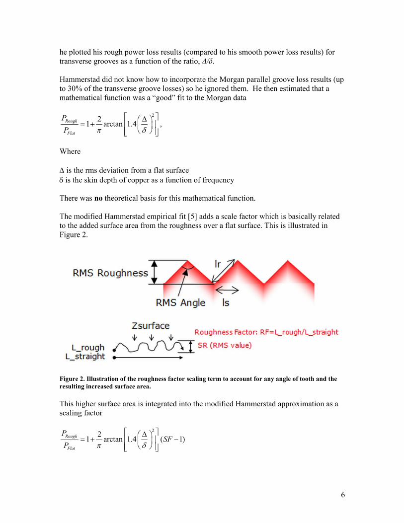
The modified Hammerstad empirical fit [5] adds a scale factor which is basically related
to the added surface area from the roughness over a flat surface. This is illustrated in
Figure 2.
Figure 2. Illustration of the roughness factor scaling term to account for any angle of tooth and the
resulting increased surface area.
This higher surface area is integrated into the modified Hammerstad approximation as a
scaling factor
2
21 arctan 1.4 ( 1)
∆ = + −
Rough
Flat
PSF
P π δ
7
When SF = 2, this expression reduces to the Hammerstad empirical mathematical
equation.
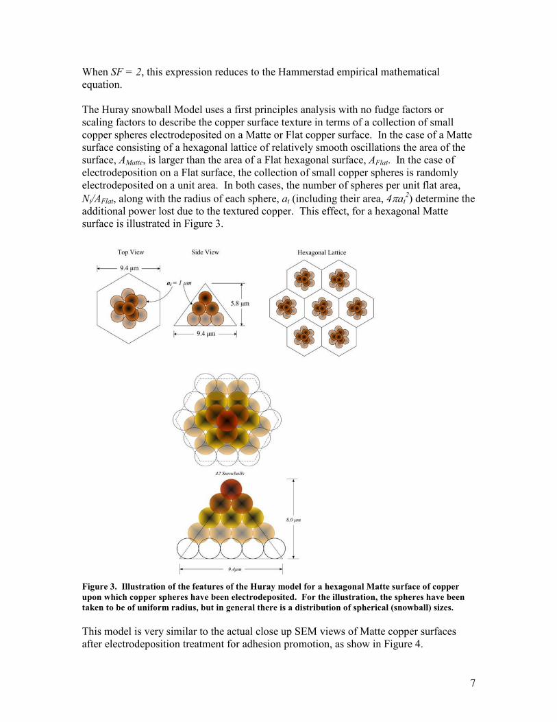
The Huray snowball Model uses a first principles analysis with no fudge factors or
scaling factors to describe the copper surface texture in terms of a collection of small
copper spheres electrodeposited on a Matte or Flat copper surface. In the case of a Matte
surface consisting of a hexagonal lattice of relatively smooth oscillations the area of the
surface, AMatte, is larger than the area of a Flat hexagonal surface, AFlat. In the case of
electrodeposition on a Flat surface, the collection of small copper spheres is randomly
electrodeposited on a unit area. In both cases, the number of spheres per unit flat area,
Ni/AFlat, along with the radius of each sphere, ai (including their area, 4πai2) determine the
additional power lost due to the textured copper. This effect, for a hexagonal Matte
surface is illustrated in Figure 3.
Figure 3. Illustration of the features of the Huray model for a hexagonal Matte surface of copper
upon which copper spheres have been electrodeposited. For the illustration, the spheres have been
taken to be of uniform radius, but in general there is a distribution of spherical (snowball) sizes.
This model is very similar to the actual close up SEM views of Matte copper surfaces
after electrodeposition treatment for adhesion promotion, as show in Figure 4.
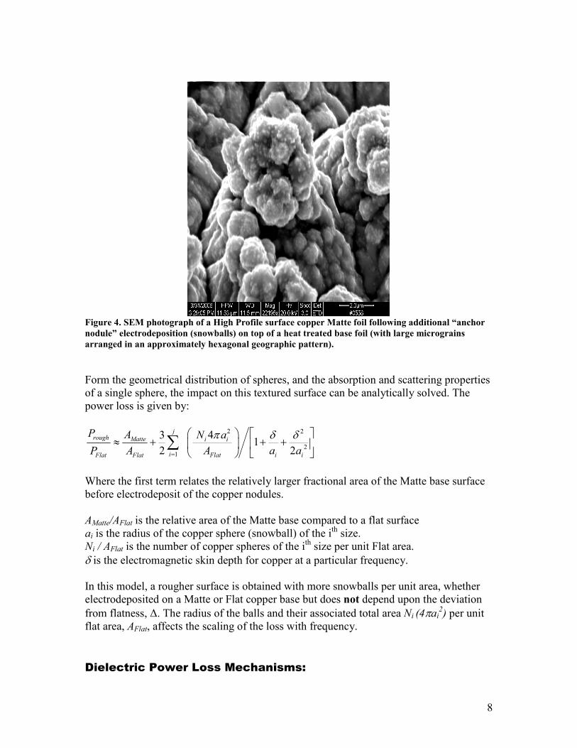
8
Figure 4. SEM photograph of a High Profile surface copper Matte foil following additional “anchor
nodule” electrodeposition (snowballs) on top of a heat treated base foil (with large micrograins
arranged in an approximately hexagonal geographic pattern).
Form the geometrical distribution of spheres, and the absorption and scattering properties
of a single sphere, the impact on this textured surface can be analytically solved. The
power loss is given by:
2 2
21
431
2 2=
≈ + + +
∑
jrough Matte i i
i Flat i iFlat Flat
P A N a
A a aP A
π δ δ
Where the first term relates the relatively larger fractional area of the Matte base surface
before electrodeposit of the copper nodules.
AMatte/AFlat is the relative area of the Matte base compared to a flat surface
ai is the radius of the copper sphere (snowball) of the ith
size.
Ni / AFlat is the number of copper spheres of the ith
size per unit Flat area.
δ is the electromagnetic skin depth for copper at a particular frequency.
In this model, a rougher surface is obtained with more snowballs per unit area, whether
electrodeposited on a Matte or Flat copper base but does not depend upon the deviation
from flatness, ∆. The radius of the balls and their associated total area Ni (4πai2) per unit
flat area, AFlat, affects the scaling of the loss with frequency.
Dielectric Power Loss Mechanisms:

9
The model used in this study to describe dielectric loss is the wideband Debye model
[10]. The simplest and most commonly used approach to implement a wideband, or an
infinite pole Debye model, is using the Svensson-Djordjevic approximation [11].
In this model, the real part of the dielectric constant is assumed to take a log dependence
on frequency. The imaginary part of the dielectric constant is related to the real part with
the Kramers-Kronig relationship. These parameters take the form of:
( )2 2
2 1
DkDk(f ) Dk log(f ) log(f )
log(f ) log(f )
∆= + −
−
And
( )2 1
(f ) 0.682 Dk 0.682Df f slope
Dk(f ) Dk(f ) log(f ) log(f ) Dk(f )
′′ε ∆ −= = =
−
There are five parameters that define the Svensson-Djordjevic approximation to the
wideband Debye model:
f1 is the low frequency range for the model
f2 is the high frequency range for the model
f is the frequency at which Dk and Df are defined
Dk at a frequency
Df at a frequency
From these five terms, the functional dependence of Dk(f) and Df(f) can be calculated.
This is inherently a causal model. Other causal models, neglected in this paper, are the
multipole Debye over-damped model and the multipole Lorentz relaxation models.
The Fundamental Problem and Solution
A First Principles Design Flow
In a perfect world, design information such as cross section information, material
properties and manufacturing processes, would be input to a simulation tool and from
first principles, with no feedback from the fab vendor, and an accurate prediction of the
performance of the interconnects would be available for integration into a system level
simulation.
Before there was so much concern about loss at frequencies higher than 1 GHz, the
industry had come close to this goal. The characteristic impedance, time delay and cross
talk features are straightforward to accurately predict. When the details about the specific
glass yarn, resin composition of each laminate layer and the process conditions like etch
back are taken into consideration, interconnect performance can be controlled and
predicted to better than 5% for frequencies below 1 GHz.

10
In the design for a target impedance or cross talk level, an accurate simulation
environment allows an engineer to realistically explore design space and make
performance, practical manufacturing capabilities and cost tradeoffs.
But, when signal data rates are in excess of 2 Gbps (with inclusion of up to the 5th
harmonic for signal bandwidths) and interconnects can exceed 40 inches in length, an
accurate representation of loss at frequencies above 5 GHz is essential. The challenge is
in being able to simulate the performance of a specific interconnect structure based on the
first principles input information from a fab vendor about their processes and material
choices.
This is the industry goal for lossy interconnects: to establish a methodology, set of tools
and a set of specific measureable input properties which will output an accurate
prediction of a specific interconnect’s performance which will closely match a real
measurement.
With such a tool, design space can be explored and the most cost effective balance in
materials choices manufacturing processes and design for acceptable loss could be found.
Finalizing this process requires more investigation in determining the best way of
characterizing surface texture and material properties, parameterizing the models and
accurately measuring the features of the manufacturing process and specific intrinsic of
materials features which affect loss.
In the mean time, another approach is being adopted to fill the gap and provide some
degree of predictability or final lot acceptance.
A Practical Approach: Feedback Based Design Flow
As an intermediate goal, one approach is to take the information from a fabricated test
coupon and extract from it the parameters and their values which would be used as input
to a simulation tool which would then accurately predict the performance of all
interconnects fabricated in the same way.
Two additional features of this process would increase the value of this approach. First
would be to allow scaling to different cross section geometries rather than just those
specific lines that look like the features of the coupon’s test line, assuming the same
materials and processes for all the layers. This allows the possibility of exploring design
space to optimize the cross section design.
As an added bonus of this process, it would be great if there was a strong correlation
between the parameter values of the mathematical expressions which results in a good fit
and specific manufacturing processes or material features. This way, the specific root
cause of the loss could be identified and direct decisions made about adjusting the design,
the manufacturing process or the materials selection to optimize the cost and performance

11
based on the actual root cause. This design process could provide some feedback to the
fab house on where to look to bring a board into closer compliance to a total loss spec.
A feedback based design flow involves the following steps:
1. Measure the S-parameters of the test lines on the coupon
2. Convert them into a useful form
3. Select the mathematical expression
4. Fit the parameters of the mathematical expression to the measured data
5. Evaluate the quality of the mathematical fit
6. Interpret the parameters in terms of design, materials or process
7. Use the parameters in a circuit simulation of the board level interconnects
8. Adjust the design to balance cost, manufacturability and performance
A key step in this process is converting the raw, measured, S-parameters of various test
lines into a format from which the material properties can be more easily extracted. This
means the artifacts from non 50-ohm lines and non-transparent launches are removed.
A variety of techniques are available to accomplish this task. For example, the launches
can be de-embedded, and then the ports re-normalized. Two lines of different length can
be measured and the generalized modal S-parameters (GMS) extracted. Or, the
measurements from multiple length lines can be combined to directly extract the complex
propagation constant for the interconnect medium using the multi-line approach [12].
These techniques are not the topic of this paper. Instead, in this paper, we explore some
of the other elements of this process; in particular, the analysis of the S-parameters with
self normalized ports obtained from both measurement and simulation, and the properties
of the various loss descriptions.
Exploring Design Space In this study, the simulated or measured 2-port S-parameters for candidate uniform
stripline transmission lines were created. In most cases, the simulations in this study were
performed with Simberian’s Simbeor [13].
To be consistent, the following geometry features were used in all simulations:
• Line width = 7 mils
• Conductor thickness = 0.7 mils ( ½ oz copper)
• Rectangular cross section
• Bulk copper conductivity
• Dielectric thickness above and below the signal conductor = 8 mils
• The typical interconnect length simulated = 1 inch
• Nominal dielectric constant @ 1 GHz = 4
• In all examples, the surface texture was applied to all copper surfaces
12
This results in close to a 50 Ohm line. The maximum return loss from 1 MHz to 40 GHz
was less than -30 dB in all cases. This means reflections have no impact on the insertion
loss results.
A simple analysis process was used to quickly identify the features of the mathematical
expression or measured data.
The time delay of the interconnect, in nsec, was extracted from the unwrapped phase of
the insertion loss using:
( )( )TD(f )[nsec] 1x unwap phase(S21) / 360 / frequency[GHz] x 1e9= −
Where
TD(f) is the time delay of the interconnect in nsec
S21 is the complex insertion loss
Frequency is the frequency of each value, in GHz
It should be noted that when unwrapping the phase of the insertion loss to get the phase
delay, a short enough frequency interval must be used so that the transitions from the
lower to the upper half of the unit circle can be accurately counted. This is especially
important when using a log freq increment.
From the time delay and the interconnect length, the effective dielectric constant can be
calculated from:
( )2
eff
11.8Dk f TD(f )[nsec]
Len[in]
=
Where
Dkeff(f) is the effective dielectric constant of the interconnect
11.8 is the speed of light in air in inches/nsec
Len is the interconnect length in inches
TD(f) is the time delay in nsec
The interconnect losses are described by the insertion loss. Assuming that the conductor
and dielectric losses can be separately described by a resistance per length and a
conductance per length the insertion loss can be written as
LenLen 0
0
R (f )S21(f )[dB] 4.24 x G (f )Z
Z
= +
Where
S21 is the insertion loss in dB
13
RLen is the resistance per length
Z0 is the characteristic impedance
GLen is the conductance per length
While we may be able to separate the conductor and dielectric losses when synthesizing
the S-parameters, there is no practical way of separating the conductor and dielectric
contributions to loss or dispersion from already existing S-parameter data. The egg has
been scrambled.
This factor creates the most significant challenge when interpreting the S-parameters of a
uniform transmission line. The impact from both conductor and dielectric mathematical
expressions are inseparably intertwined in the loss and dispersion. The only hope of
gaining some insight into their relative contributions lies in their different frequency
dependences.
Each conductor and dielectric mathematical expressions will contribute a different
frequency dependence in both loss and dispersion depending on the parameter values
selected. This is the focus of the analysis here. The analysis of the frequency dependence
of each loss mathematical expression can only be done as a numerical study, where each
term can be isolated and the impact on the frequency dependence of loss and dispersion
evaluated.
The frequency dependence of the insertion loss, in dB, arises from the separate frequency
dependence of the resistance per length and conductance per length. To first order, the
resistance should vary roughly with the square root of frequency, dominated by skin
depth effects and the propagating medium permittivity should vary linearly with
frequency due to the motion of the dipoles.
It’s possible to quickly identify the frequency dependence of the insertion loss and which
term dominates by taking the unusual step of plotting the insertion loss, in dB, and
frequency on a log-log scale and comparing the slope of the curve to a slope of ½ and
slope of 1. Of course to plot the insertion loss on a log scale, the absolute value of the
insertion loss must be used.
An example of the insertion loss vs. frequency on a log-log scale for the case of a
measured 10 inch long stripline in an FR4 type material is shown in Figure 5.
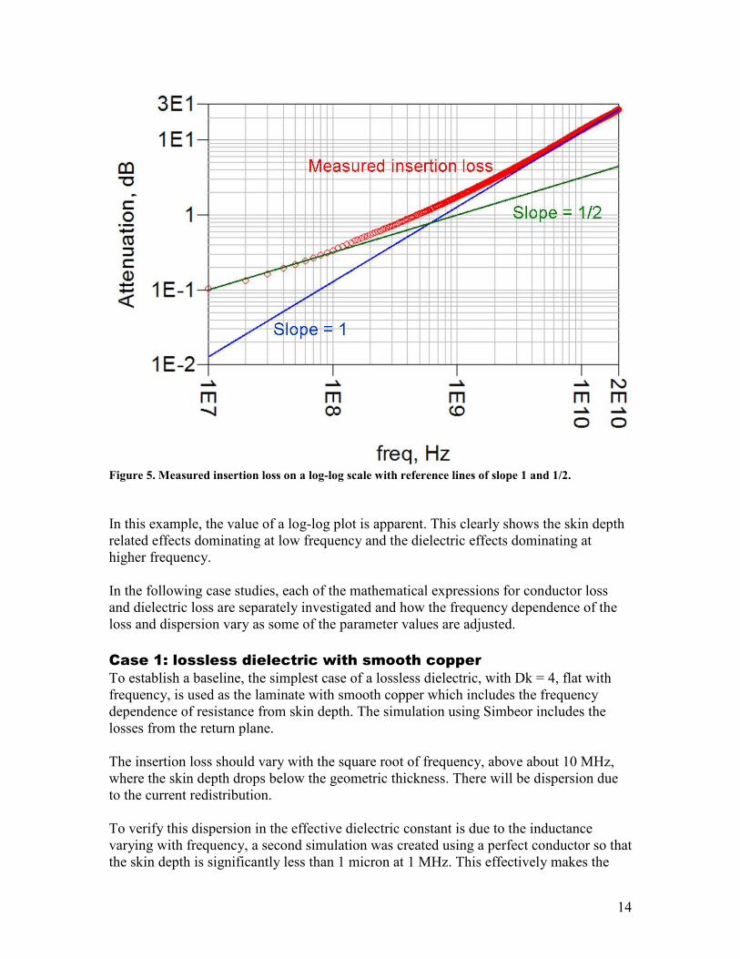
14
Figure 5. Measured insertion loss on a log-log scale with reference lines of slope 1 and 1/2.
In this example, the value of a log-log plot is apparent. This clearly shows the skin depth
related effects dominating at low frequency and the dielectric effects dominating at
higher frequency.
In the following case studies, each of the mathematical expressions for conductor loss
and dielectric loss are separately investigated and how the frequency dependence of the
loss and dispersion vary as some of the parameter values are adjusted.
Case 1: lossless dielectric with smooth copper
To establish a baseline, the simplest case of a lossless dielectric, with Dk = 4, flat with
frequency, is used as the laminate with smooth copper which includes the frequency
dependence of resistance from skin depth. The simulation using Simbeor includes the
losses from the return plane.
The insertion loss should vary with the square root of frequency, above about 10 MHz,
where the skin depth drops below the geometric thickness. There will be dispersion due
to the current redistribution.
To verify this dispersion in the effective dielectric constant is due to the inductance
varying with frequency, a second simulation was created using a perfect conductor so that
the skin depth is significantly less than 1 micron at 1 MHz. This effectively makes the

15
current distribution in the simulated frequency range constant and just on the surface of
the conductors so there should be no dispersion.
Figure 6 shows the results for case 1, giving an indication of the sort of insertion loss and
dispersion just from smooth copper and a perfect conductor for this 7 mil wide uniform
transmission line.
Figure 6. Insertion loss and dispersion for smooth copper. The square root of frequency is an
excellent fit to the insertion loss, while the linear dependency with frequency is a poor fit even at the
highest frequency.
The dispersion from the current re-distribution dominates the effective dielectric constant
below 1 GHz. Above 5 GHz is it negligible.
Case 2: Hammerstad mathematical expression for surface
roughness
The Hammerstad mathematical expression is an empirical approximation to the 2
dimensional triangular surface features used by Samuel Morgan [14] and with a linear
distance up and down over the peaks and valleys that is twice the straight line distance.
This effectively means the triangles have a 60 degree angle from the surface.
In this example, a lossless dielectric was used but the surface roughness was fit with the
Hammerstad mathematical expression using three values of the rms surface roughness, 1
micron, 3 microns and 5 microns. The insertion loss and effective dielectric constant are
shown in Figure 7.
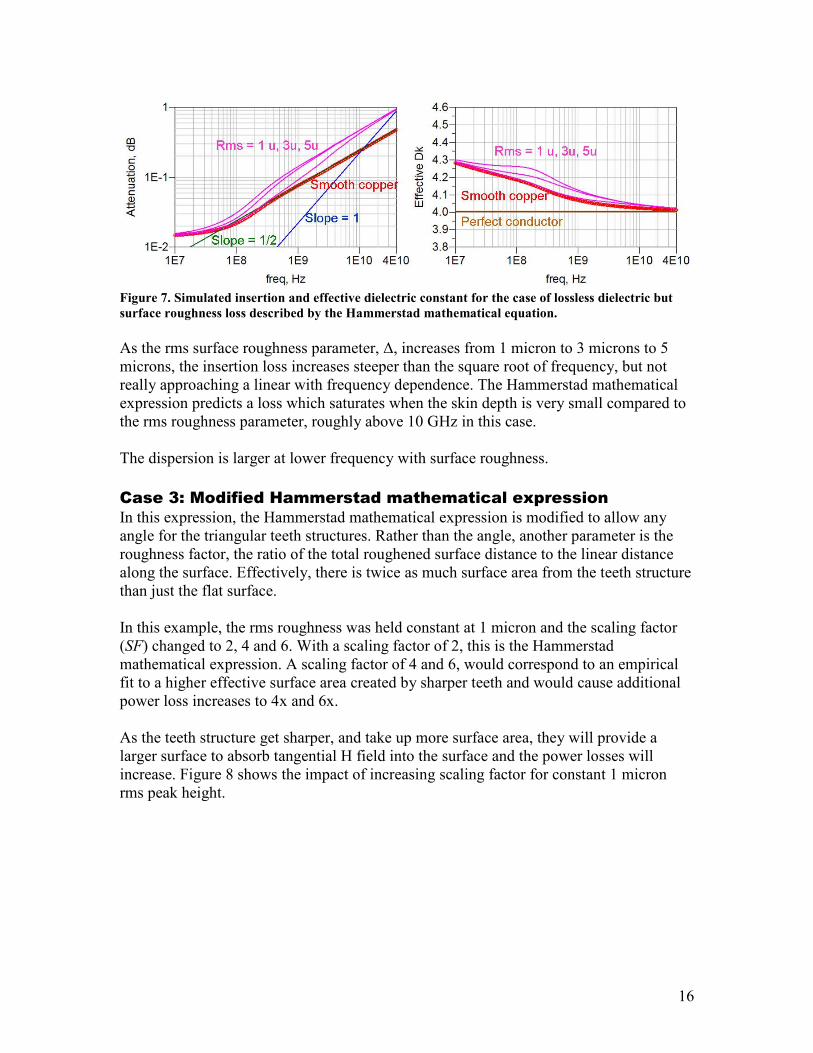
16
Figure 7. Simulated insertion and effective dielectric constant for the case of lossless dielectric but
surface roughness loss described by the Hammerstad mathematical equation.
As the rms surface roughness parameter, ∆, increases from 1 micron to 3 microns to 5
microns, the insertion loss increases steeper than the square root of frequency, but not
really approaching a linear with frequency dependence. The Hammerstad mathematical
expression predicts a loss which saturates when the skin depth is very small compared to
the rms roughness parameter, roughly above 10 GHz in this case.
The dispersion is larger at lower frequency with surface roughness.
Case 3: Modified Hammerstad mathematical expression
In this expression, the Hammerstad mathematical expression is modified to allow any
angle for the triangular teeth structures. Rather than the angle, another parameter is the
roughness factor, the ratio of the total roughened surface distance to the linear distance
along the surface. Effectively, there is twice as much surface area from the teeth structure
than just the flat surface.
In this example, the rms roughness was held constant at 1 micron and the scaling factor
(SF) changed to 2, 4 and 6. With a scaling factor of 2, this is the Hammerstad
mathematical expression. A scaling factor of 4 and 6, would correspond to an empirical
fit to a higher effective surface area created by sharper teeth and would cause additional
power loss increases to 4x and 6x.
As the teeth structure get sharper, and take up more surface area, they will provide a
larger surface to absorb tangential H field into the surface and the power losses will
increase. Figure 8 shows the impact of increasing scaling factor for constant 1 micron
rms peak height.

17
Figure 8. Simulated insertion and effective dielectric constant for the case of lossless dielectric but
surface roughness losses given by a modified Hammerstad mathematical expression in which only
the scaling factor is increasing for a fixed 1 u rms peak height.
In this example, increasing scaling factor means increasing losses from the conductor,
and more importantly, in some frequency regions, the losses increase close to a linear
frequency rate. The dispersion also increases in the high frequency region.
Case 4: Huray snowball model
There are three parameter that define the Huray first principles snowball model:
ai, the radius of the ith
sphere,
AMatte/AFlat, the relative area of a Matte base compared to a Flat base area
Ni (4πai2)/AFlat, the total area of the additional spheres compared to a Flat base area.
The total area of the additional spheres per unit Flat area means more surface area and
absorption of tangential H fields into the electrodeposited conductor anchor nodules than
that provided by AMatte/AFlat. However, each additional loss term is dependent upon
frequency according to 2 2
21
431
2 2
j
i i
i Flat i i
N a
A a a
π δ δ
=
+ +
∑
The factor of 3/2 and the frequency dependence in the denominator occur from the dipole
approximation for copper snowballs (i.e. to first order they can be modeled as copper
spheres).
In exploring the impact of these parameters on the loss and dispersion, two ranges are
considered. In the first example, a fixed ball diameter, 1 micron, and number of balls, 30,
was used for various base areas of (10 microns)2, (7 microns)
2 , (5 microns)
2 and (3
microns)2. This effectively increases the surface area density for absorption. The smaller
the base area the higher the expected loss. Figure 9 shows the simulated insertion loss and
dispersion for these four values of base areas.

18
Figure 9. Simulated results using the Huray snowball model for the case of 30 balls, each 1 micron in
diameter, with different flat base areas. I would like to see the code that deduced this chart to verify its
validity.
.
It is interesting to note that as the density of ball area per unit flat area increases, the
slope of the insertion loss increases and approaches a linear frequency dependence. The
dispersion is only slightly affected by the density until the density gets very high.
As a second example, the tile base area of (5 microns)2 was selected, with 30 balls of
diameter 2 microns, 1 micron and 0.5 micron. Again the assumption of uniform ball size
was made.
As the ball diameter decreases two effects happen. The frequency at which the excess
loss turns on increases in frequency as it scales with the ball radius to skin depth value.
Secondly, as the ball diameter decreases, the effective surface area available for
absorption and loss decreases and the total excess loss decreases. This is related to the
square of the ball diameter.
These two effects are seen in the simulated examples shown in Figure 10.
Figure 10. Simulated insertion loss and dispersion with the Huray snowball model, changing just the
ball diameter from 2 microns to 1 micron to 0.5 micron but assuming a constant base area of (0.5
microns)2 and uniform size balls.
In this example, it’s clear how sensitive the results are to the ball diameter. This one
parameter affects when the loss turns on, how much loss and how much dispersion
19
results. Large nodule ball area per unit base area generates a lot of loss and has a big
impact on dispersion.
These mathematical expressions of loss all point out that it’s the increased roughened
surface area which most strongly affects the amount of loss from surface texture. This
suggests that to engineer the lowest loss surface texture while still providing some
adhesion, a selectively patterned surface should be used. A nominally flat surface should
be the starting place, with a patterned surface treatment spaced every mil or more with
large features (small surface area compared to the conductor volume). This would cut the
surface area by as much as 10x to 20x, reducing the surface power loss by a comparable
amount.
While the modified Hammerstad mathematical expression and the Huray snowball model
use different parameters, they both have a parameter which describes a surface deviation
and a surface area factor. Either approach might be a candidate for comparing to the
measured loss contribution from surface texture.
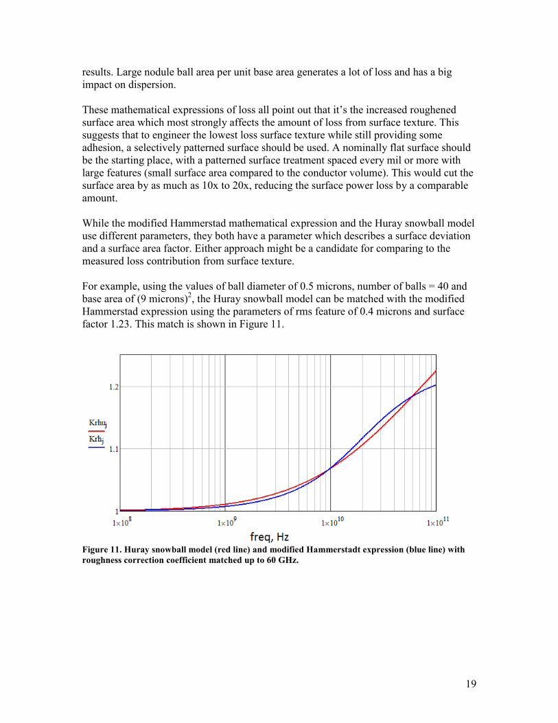
For example, using the values of ball diameter of 0.5 microns, number of balls = 40 and
base area of (9 microns)2, the Huray snowball model can be matched with the modified
Hammerstad expression using the parameters of rms feature of 0.4 microns and surface
factor 1.23. This match is shown in Figure 11.
Figure 11. Huray snowball model (red line) and modified Hammerstadt expression (blue line) with
roughness correction coefficient matched up to 60 GHz.

20
Case 5: Dielectric loss model: relationship between Dk slope and
Df
In the wide band Debye model with the Svensson-Djordjevic approximation, the
dielectric constant varies linearly with the log of frequency. The slope of the dielectric
constant with the log of the frequency, is a direct measure of the dissipation factor. In
fact, the dissipation factor is given by:
( )2 1
(f ) 0.682 Dk 0.682Df f slope
Dk(f ) Dk(f ) log(f ) log(f ) Dk(f )
′′ε ∆ −= = =
−
In the following example, the five parameters for the wideband Debye model were used:
Dk = 4
Df = 0.02, 0.01, 0.005, 0.002
f = 1 GHz
f1, the low frequency limit = 100 kHz
f2, the high frequency limit = 100 GHz.
Figure 12 shows the simulated insertion loss and dispersion for the case of a perfect
conductor but the dielectric properties above.
Figure 12. Simulated loss and dispersions for perfect conductor and wide band Debye model where
only the Df is varied from 0.02, 0.01, 0.005, 0.002.
There are two important features of the wideband Debye model in this example. The
insertion loss from just dielectric loss, shows a linear dependence on frequency. The
slope on the log-log scale matches the reference slope of 1.
Secondly, as expected, the slope of the effective dielectric constant over frequency is
related to the dissipation factor. The lower the dissipation factor, the flatter the dielectric
constant over frequency and the less the dispersion. Though the vertical scale on the
graph is linear, for small variations, the log of a number and the number have the same
relative difference.

21
A Suggested Methodology This analysis points out that while it is not possible to directly separate the conductor and
dielectric loss in the measured response of a transmission line sample, it may be possible
to find a set of parameters which match the measured performance of measured samples.
The input to a typical model that most simulators understand is:
the cross section parameters:
h, dielectric thickness
w, line width
t, conductor thickness
The conductor loss parameters:
Copper Conductivity
Modified Hammerstad model: rms value, scale factor
Huray snowball model: relative Matte to Flat base area, ball diameter, number of balls
per unit Flat area
Dielectric loss parameters:
Dk
Df
At f
f1 low freq limit
f2 high freq limit
Some insight into the behavior of a sample can be gained by comparing the measured
response with the simulated response which includes just some of the mathematical
expression features. The starting place can be the cross section parameters based on the
known sample properties, the smooth copper losses and the lossless dielectric properties.
The copper conductivity parameter can be matched to the low frequency loss and the Dk
parameter matched to the 1 GHz measured dielectric constant. Using values of copper
conductivity and Dk = 4.33, the comparison between measured and simulated responses
are shown in Figure 13.
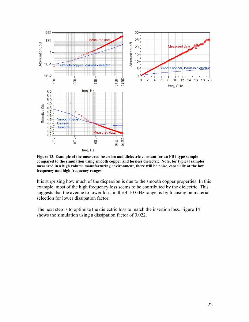
22
Figure 13. Example of the measured insertion and dielectric constant for an FR4 type sample
compared to the simulation using smooth copper and lossless dielectric. Note, for typical samples
measured in a high volume manufacturing environment, there will be noise, especially at the low
frequency and high frequency ranges.
It is surprising how much of the dispersion is due to the smooth copper properties. In this
example, most of the high frequency loss seems to be contributed by the dielectric. This
suggests that the avenue to lower loss, in the 4-10 GHz range, is by focusing on material
selection for lower dissipation factor.
The next step is to optimize the dielectric loss to match the insertion loss. Figure 14
shows the simulation using a dissipation factor of 0.022.
23
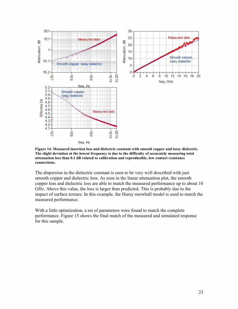
Figure 14. Measured insertion loss and dielectric constant with smooth copper and lossy dielectric.
The slight deviation at the lowest frequency is due to the difficulty of accurately measuring total
attenuation less than 0.1 dB related to calibration and reproducible, low contact resistance
connections.
The dispersion in the dielectric constant is seen to be very well described with just
smooth copper and dielectric loss. As seen in the linear attenuation plot, the smooth
copper loss and dielectric loss are able to match the measured performance up to about 10
GHz. Above this value, the loss is larger than predicted. This is probably due to the
impact of surface texture. In this example, the Huray snowball model is used to match the
measured performance.
With a little optimization, a set of parameters were found to match the complete
performance. Figure 15 shows the final match of the measured and simulated response
for this sample.

24
Figure 15. Final match of the measured response and simulated response using wideband Debye
model, smooth copper and Huray snowball model.
This same process can be applied to a variety of samples. An example of another
measured transmission line sample with a low profile (AMatte/AFlat=1) is shown in Figure
16.
7in Low
Profile
Trace
Correlation
VNA Measurement
Huray Model:
50 uniform spheres,
0.5um radius
5000x
4 µm peak to valley deviation
Figure 16. Insertion loss measurements on a 7 inch Low Profile trace as a function of frequency
(shown in blue) compared to the Huray snowball model (in green) with the further approximations
AMatte/AFlat≈1 and Ni/AFlat=50 uniform spheres per (100 micron)2 area shown in the red hexagonal
structure at lower left.

25
As a final example, 2-inch and 4-inch long Megtron6 stripline transmission lines,
courtesy of Molex Corp. were measured. A wideband Debye model with the modified
Hammerstad expression were fit to the insertion loss and group delay. Figure 17 shows
the excellent comparison between measured and simulated results.
Figure 17. Measured insertion loss and group delay for Megtron6 samples compared with the
simulated values using a wideband Debye model and a modified Hammerstad approximation with
values of Dk = 3.7, Df = 0.002 and SR = 0.3 u and RF = 5.
Conclusion While it is still not practical to take information obtained directly from a fab vendor and
turn this into a first principles model which accurately describes the complete
performance of an interconnect, it is practical, in a variety of material systems to take the
measured response from a test coupon and fit parameters associated with conductor and
dielectric loss.
The dielectric loss can be modeled with a wideband Debye model and the surface texture
of copper can be described with a variety of mathematical expressions. By fitting the
measured insertion loss and effective dielectric constant, a complete description of a
transmission line can be extracted from manufacturing test coupons in some samples
using just a few parameters.
These parameters can be used as input to a variety of popular simulators to create
scalable transmission line models for any interconnect structure. These parameters also
may be useful in providing some insight into where to attack for reduced loss.

26
References
1. E. Bogatin, D. DeGroot and A. Blankman “A Practical Approach for Using
Circuit Board Qualification Test Results to Accurately Simulate High Speed
Serial Link Performance”, DesignCon 2012
2. Y. Shlepnev, C. Nwachukwu, Practical methodology for analyzing the effect of
conductor roughness on signal losses and dispersion in interconnects,
DesignCon2012, Feb. 1st, 2012, Santa Clara, CA.
3. Y. Shlepnev, A. Neves, T. Dagostino, S. McMorrow, “Practical identification of
dispersive dielectric models with generalized modal S-parameters for analysis of
interconnects in 6-100 Gb/s applications”, in Proc. of DesignCon 2010.
4. G. Palasantzas, J.T.M. De Hosson, The effect of mound roughness on the
electrical capacitance of thin insulating film, Solid Stage Comm. V. 118, 2001, p.
203-206
5. A. Albina at all, Impact of the surface roughness on the electrical capacitance,
Microelectronics Journal, Volume 37, Issue 8, August 2006, Pages 752-758
6. S. Hall and H. Heck, Advanced Signal Integrity for High-Speed Digital Designs,
Wiley-IEEE press, 2009.
7. E. Bogatin, Signal and Power Integrity- Simplified, Prentice Hall, 2009
8. P. G. Huray, The Foundations of Signal Integrity, Wiley-IEEE press, 2009.
9. E.O. Hammerstad, Ø. Jensen, “Accurate Models for Microstrip Computer Aided
Design”, IEEE MTT-S Int. Microwave Symp. Dig., p. 407-409, May 1980.
10. E. Bogatin, D. DeGroot, C. Warwick, S. Gupta, “Frequency Dependent Material
Properties, so what?” DesignCon 2010.
11. Djordjevic, R.M. Biljic, V.D. Likar-Smiljanic, T.K.Sarkar, Wideband frequency
domain characterization of FR-4 and time-domain causality, IEEE Trans. on
EMC, vol. 43, N4, 2001, p. 662-667.
12. D.C. DeGroot, J.A. Jargon, and R.B. Marks, Multiline TRL Revealed, 60th
ARFTG Conf. Dig., pp. 131-155, Dec, 2002
13. Simbeor 2011 Electromagnetic Signal Integrity Software, www.simberian.com
14. S.P. Morgan Jr., “Effect of Surface Roughness on Eddy Current Losses at
Microwave Frequencies,” Journal of Applied Physics, Vol. 20, p. 352-362, April,
1949.