weighted area technique for electromechanically enabled
TRANSCRIPT

Weighted Area Technique for ElectromechanicallyEnabled Logic Computation With Cantilever-Based
NEMS SwitchesShruti Patil1, Min-Woo Jang1, Chia-Ling Chen1, Dongjin Lee2, Zhijang Ye2, Walter E Partlo III3,
David J. Lilja1, Stephen A. Campbell1, and Tianhong Cui2
1Department of Electrical and Computer Engineering, University of Minnesota2Department of Mechanical Engineering, University of Minnesota
3Department of Chemistry, University of Minnesota
Abstract—Nanoelectromechanical systems (NEMS) is anemerging nanoscale technology that combines mechanical andelectrical effects in devices. A variety of NEMS-based deviceshave been proposed for integrated chip designs. Amongst themare near-ideal digital switches. The electromechanical principlesthat are the basis of these switches impart the capability ofextremely low power switching characteristics to digital circuits.NEMS switching devices have been mostly used as simpleswitches to provide digital operation, however, we observe thattheir unique operation can be used to accomplish logic functionsdirectly. In this paper, we propose a novel technique called‘weighted area logic’ to design logic circuits with NEMS-basedswitches. The technique takes advantage of the unique structuralconfigurations possible with the NEMS devices to convert thedigital switch from a simple ON-OFF switch to a logical switch.This transformation not only reduces the delay of complexlogic units, but also decreases the power and area of theimplementation further. To demonstrate this, we show the newdesigns of the logic functions of NAND, XOR and a three inputfunction Y = A + B.C, and compose them into a 32-bit adder.Through simulation, we quantify the power, delay and areaadvantages of using the weighted area logic technique over astandard CMOS-like design technique applied to NEMS.
I. INTRODUCTION
The emerging technology of Nanoelectromechanical Sys-tems (NEMS) is an advancement of the fabrication of elec-tromechanical devices into nanoscale regimes. Digital switchesthat are implemented using the NEMS technology show sev-eral superior characteristics, such as zero leakage currents,high on-current capabilities and the potential for high-speed,low-Vt (threshold voltage of devices) operation. In the lightof the growing power issues in digital designs that use CMOStransistors, the near-ideal OFF-state characteristics of theNEMS switches are particularly attractive.
A number of published works have used NEMS switchesin digital designs and shown their potential to reduce powerconsumption to a great extent [1], [2]. These ideas are basedon a variety of device structures that have been proposed forNEMS-based switches([1], [3], [4], [5]). With different devicestructures, the applicability of the devices in digital designsituations changes, however, most structures have been used
as simple switches that use a combination of electrostatic andmechanical forces for actuation and release. In this work, weobserve that the unique electromechanical operation of thedevice need not be restricted to a simple switch, but canbe used to derive logic functions directly. This idea furtherallows for novel logic design strategies for NEMS devices.In this paper, we describe a logic technique called ‘weightedarea logic’ (WAL) design, with which logic functions areembedded into the device structure itself. By transformingelectromechanical properties into a direct logic capability, thedevice gets converted into a logical switch. This reduces thenumber of devices required to implement a logic function,which leads to a decrease in delay, power and area of theimplementation.
To demonstrate and evaluate the proposed logic designtechnique, we use Carbon-nano-tube (CNT) based NEMScantilever switches. Amongst the materials that have beenstudied for NEMS devices (for example tungsten, poly-silicon[1], CNT [3], [6]), CNT films possess the most promisingmaterial properties, such as low mass density, high yieldstrength and high Young’s modulus [6]. Theoretically, thisleads to the potential to operate in Gigahertz ranges with a low-Vt ([7], [8]). Experimentally, two-terminal NEMS switchesoperating at about 600ps have been demonstrated in ([8], [9]).Using the proposed logic design technique with CNT-basedNEMS devices, we show the design of a 32-bit adder.We findthat the WAL design strategy has the potential to decreasethe delay as well as the power, which together results in aconsiderable reduction in the energy and energy-delay productof the adder. The proposed logic design technique is intendedto be a general concept that applies to any NEMS switchingstructure which relies on electromechanical principles.
II. CNT BASED NEMS-CANTILEVER DEVICE ANDOPERATION
A cantilever-based nano-electro-mechanical (NEMS) switchis actuated by a combination of electrical and mechanicaleffects in the device. The NEMS-CNT switch that we use inthis paper is a 3-terminal structure, with anchor (A), gate (G)978-3-9810801-8-6/DATE12/ c©2012 EDAA

and drain (D) terminals. A cantilever beam fabricated witha single wall carbon nanotube (SWCNT) thin film extendsfrom the anchor to the drain terminal, forming a CNT-basedconducting channel in the switch. Fig. 1(a) shows the devicestructure, where the cantilever beam stands freely above thedrain. In order to operate the device, a gate voltage is appliedto create a voltage difference between the gate and the anchor.This induces opposite charges on the gate and the cantilever,creating an electrostatic force of attraction between them. Ifthe difference in the voltages on the terminals exceeds a certainthreshold value called as pull-in voltage VPI , the electrostaticforces exert a sufficient pull-in force on the cantilever thatforces it to make contact with the drain. This connects theanchor and drain terminals, thus closing the ‘switch’. Whenthe electrostatic force of attraction disappears, the pull-in forcedisappears, however, in the closed position, there exists aspring restoring force in the cantilever due to its mechanicalproperties. Therefore the cantilever springs back to its freelystanding initial position, resulting in an ‘open’ switch. To avoidshorting the source to the gate, a thin insulator can be placedon top of the gate electrodes. This is achieved by using ahigh permittivity material such as HfO2, to minimize anyreduction in the electrostatic force [10].
! "
#$%
%&
!
"
#$%
%'
"(!) #$%(* "(!) "(!)(*
! + ,
(*
! !+ +,
!
+
+
,
!
"(!)
(*
#$%
(*
"(!)
! ,+
+-./0..1 +-./0..1 #2345678! ,+
+-./0..1 0../+-.1 #239490/!1
:;-
(a) FreestandingCantilever
! "
#$%
%&
!
"
#$%
%'
"(!) #$%(* "(!) "(!)(*
! + ,
(*
! !+ +,
!
+
+
,
!
"(!)
(*
#$%
(*
"(!)
! ,+
+-./0..1 +-./0..1 #2345678! ,+
+-./0..1 0../+-.1 #239490/!1
:;-
(b) Fixed-Fixedbeam
! "
#$%
%&
!
"
#$%
%'
"(!) #$%(* "(!) "(!)(*
! + ,
(*
! !+ +,
!
+
+
,
!
"(!)
(*
#$%
(*
"(!)
! ,+
+-./0..1 +-./0..1 #2345678! ,+
+-./0..1 0../+-.1 #239490/!1
:;-
(c) TopView of(b)
! "
#$%
%&
!
"
#$%
%'
"(!) #$%(* "(!) "(!)(*
! + ,
(*
! !+ +,
!
+
+
,
!
"(!)
(*
#$%
(*
"(!)
! ,+
+-./0..1 +-./0..1 #2345678! ,+
+-./0..1 0../+-.1 #239490/!1
:;-
(d) Open Switch
! "
#$%
%&
!
"
#$%
%'
"(!) #$%(* "(!) "(!)(*
! + ,
(*
! !+ +,
!
+
+
,
!
"(!)
(*
#$%
(*
"(!)
! ,+
+-./0..1 +-./0..1 #2345678! ,+
+-./0..1 0../+-.1 #239490/!1
:;-
(e) Closed Switch
Fig. 1. (a)-(c)NEMS-CNT Device Structures; (d)-(e)Voltage biases onterminals for different logic states
The simple cantilever shown in Fig. 1(a) is very dense, butis quite sensitive to the effects of stress in the film, whichcan lead to significant changes in the zero-bias gap betweenthe gate and the electrode. A more stable structure is shownin Fig. 1(b), where the cantilever beam is supported on bothsides by the anchor terminals. This structure, as seen in thetop view is shown in Fig. 1(c). The behavior of the device isfundamentally similar to the first structure, but is less sensitiveto process variables. Furthermore, it provides important newdesign capabilities by incorporating multiple gate electrodesinto a single device. The biasing of the anchor and gateterminals in the open and closed states is shown in Fig.1(d)-1(e). Voltage V dd is chosen to be 1 − 2 times that of VPI
according to the required noise margin levels. NEMS-CNTswitches that operate on this principle have been demonstratedin ([3], [6], [8]). With suitable materials, their potential tooperate at pull-in voltages of 100mV has also been investigated[11], making them promising devices for use in low-power
digital designs.
A. Equivalence to a transistor
Digital designs using the MOSFET technology have tra-ditionally utilized the ON/OFF switch-like behavior of thetransistors to accomplish logic functions. In fact, the behaviorof a NEMS-CNT device resembles that of a digital CMOSswitch in that the voltage between the anchor and the gateacts as the controlling voltage, and determines the ON orOFF state, similar to a transistor operation. Therefore, anequivalent NEMS-CNT-based logic design can be derived byreplacing the PMOS and NMOS devices in a CMOS-baseddesign with appropriately biased NEMS-CNT devices. We willrefer to this design style as the standard design techniquefor NEMS. In order to demonstrate that the standard designtechnique applies to real NEMS devices, we demonstrated aNAND logic gate fabricated using a NEMS-CNT device witha fixed-fixed beam structure. The fabrication process, devicedetails and characterization curves are presented in [10]. Thisexperimentally verified two aspects of designing with NEMS-CNT switches: (1) the behavioral similarity between MOSFETswitches and NEMS-CNT devices, and (2) the feasibility ofderiving logic circuits by a simple replacement of CMOSdevices by NEMS-CNT switches.
B. Model for circuit simulation
To assist in circuit simulation, the behavior of the devicecan be abstracted into a parameterized NEMS device model.Functionally, the NEMS cantilever device is a 3-terminalswitch with a finite on-resistance Ron. Its switching mecha-nism has a mechanical delay Tmech. Switching occurs at pull-in voltage of VPI . For any gate voltage less than VPI , thedevice current is zero. While the gate-cantilever capacitanceCGC can be modeled as a dynamic capacitance that describesthe electromechanical operation, we note that the internalcapacitances of the device are extremely low. For the gate, thisis due to the large gap, typically about 20nm, compared to a1nm equivalent oxide thickness of a fully scaled gate oxide.For the source and drain, the low capacitance is because thereare no junctions in the device. It is built in a low dielectriccontact material (SiO2), instead of in a semiconductor. Thus,the capacitance of the device as experienced by a circuit stemsmainly from the self capacitances of the wire associated withthe three terminals of the anchor, gate and the drain, i.e. Ca,Cg and Cd respectively. Another significant behavior exhibitedby the NEMS-CNT devices is their asymmetry in rise and falltimes [6]. The rise time due to the device switching ON isabout 80-90% higher than the fall time measured when thedevice switches OFF.
Based on this operation, we developed a Verilog-A modelfor the NEMS devices for circuit-level simulation of complexlogic units that can allow us to compare between differentdesigns. It models the NEMS-CNT device as a 3-terminalswitch with five parameters Ron, Tmech (= TON ), VT , Cnode
and Asymmetry Ratio (TOFF /TON ). This simplistic behav-ioral model allows us to fit measured device values in the

model, while giving the flexibility to observe the sensitivityof the device for different parameters along with preliminaryperformance evaluation and projection for different applica-tions.
III. CANTILEVER-BASED NANOMECHANICAL LOGICDESIGNS
While one feasible technique of designing with the NEMS-CNT devices is by using the classic complementary standarddesign technique, the devices also possess a number of uniqueproperties. For example, the behaviors of the PMOS andNMOS devices in a CMOS implementation can be obtained byapplying appropriate biases on the same device structure. Thissimplifies the fabrication process significantly and reduces thearea. Secondly, the pull-in voltage of an individual devicecan be easily varied by varying the structure of a device.This in turn, enables the devices to be manufactured asmore complex structures. On the flip side, the devices sufferfrom a large mechanical delay relative to an electrical delay.Therefore, it is desired to reduce the total delay of a logiccircuit. Taking into account these strengths and challenges ofthe devices, we propose an electromechanical design strategycalled as ‘weighted area logic design’ that relies on the elec-tromechanical operation of the devices to implement NEMS-CNT based logic structures. By incorporating both electricaland mechanical effects to produce a logical result directly,the number of devices in the maximum combinational pathare reduced, resulting in faster logic computation. Also, byintegrating the logic functionality into the device structure,the logic circuits that are produced result in smaller structuresthan a corresponding standard implementation.
A. Weighted Area Logic (WAL) Design Concept
The amount of electrostatic force formed between thecantilever and the gate depends upon many factors, including(1) the voltage bias on the two terminals; (2) the area of thecantilever and the gate resulting in the pull-in forces; (3) thedistance between the cantilever and the gate. The weightedarea logic design strategy exploits the second factor. The pull-in force experienced by the cantilever is proportional to theoverlap area between the cantilever and the gate. By changingthe cantilever-gate overlap area, the magnitude of effect of thegate on the cantilever can be controlled. The larger the overlaparea, the higher is the effect, or the ‘weight’, of the gate.With this ability, instead of relying on switch-based electroniccircuit to compute a logical output, we are able to leveragethe electromechanical properties of the devices to obtain thelogical result directly.
When a larger impact of an input is required on the output,a device with a larger gate-cantilever overlap area is designed.For example, in the expression Y = A + B.C, the inputA affects the logic-high output individually, while inputsB and C affect the logic-high result in combination. Thus,the contribution of input A in the function is larger, andnecessitates a larger impact on the cantilever by input A aloneas compared to that of inputs B and C alone. The contribution
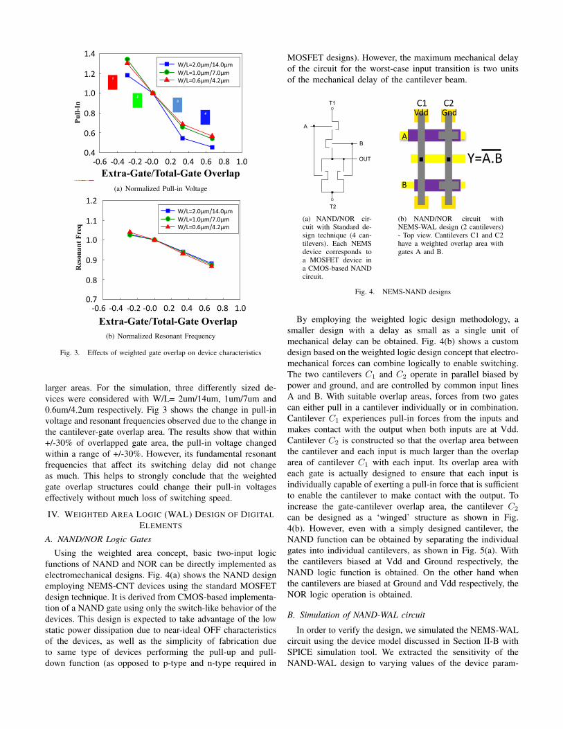
Fig. 2. Weighted gate overlap structures simulated
of an input to the logic-high and logic-low states in a truthtable is evident when the logic design is expressed in theform of a sum-of-products (SOP) (or product-of-sum (POS))expression. These expressions describe the desired output asa logical function of the inputs. For instance, when inputsare OR-ed together, all inputs affect the output equally andindependently. On the other hand, when inputs are AND-edtogether, this indicates that the inputs affect the output incombination.
We convert this observation into the weighted area logicdesign approach. An input that affects the output individuallyis designed so that it exerts sufficient mechanical pull-in on acantilever by itself. On the other hand, inputs that affect theoutput in combination are designed and placed so that they areable to pull-in a cantilever only in combination. To increasethe pull of a gate on the cantilever, its area of overlap withthe cantilever is increased, while to decrease its pull on thecantilever, its area of overlap is reduced. In terms of weights,the inputs that are OR-ed are alloted equal weightage, eachof which is the maximum weightage for the determination ofthe output. The inputs that are AND-ed are also given equalweightage, however the sum of the weights is the maximumweightage. Thus, a cantilever–based design can be directlyderived from an SOP or a POS expression. Since the logicaloperation is partly incorporated into the physical structure, theresultant design occupies a lesser chip area than a design withdevices that act as 3-terminal switches equivalent to a standardMOSFET operation.
B. Device-level simulation of the WAL Concept
To first validate the weighted area theory, we used a MEMSdevice simulator called Coventorware. The simulator enablesa structural verification of the device layout and allows usto see the effects of the weighted gate overlap structures.Fig. 2 shows the four structures that were studied. With anormal structure as a baseline, the gate-cantilever overlaparea was varied as −28%,+33% and +67% to observe thechanges in pull-in voltages for a smaller area as well as
Prof. Campbell Research Group
July 25th , 2011 - 3 -
2
1
3
4
Extra-Gate/Total-Gate Overlap
Pu
ll-I
n
!"#$
!"%$
!"&$
&"'$
&"($
)&"($ )&"#$ )&"%$)&"&$ &"%$ &"#$ &"($ &"'$ !"&$&"#$
*+,-%"&./+!#"&./$
*+,-!"&./+0"&./$
*+,-&"(./+#"%./$
(a) Normalized Pull-in Voltage
Prof. Campbell Research Group
July 25th , 2011 - 3 -
Extra-Gate/Total-Gate Overlap
!"#$
!"!$
!"%$
%"&$
%"'$
(%")$ (%"*$ (%"#$(%"%$ %"#$ %"*$ %")$ %"'$ !"%$%"+$
,-./#"%01-!*"%01$
,-./!"%01-+"%01$
,-./%")01-*"#01$
Res
on
an
t F
req
(b) Normalized Resonant Frequency
Fig. 3. Effects of weighted gate overlap on device characteristics
larger areas. For the simulation, three differently sized de-vices were considered with W/L= 2um/14um, 1um/7um and0.6um/4.2um respectively. Fig 3 shows the change in pull-involtage and resonant frequencies observed due to the change inthe cantilever-gate overlap area. The results show that within+/-30% of overlapped gate area, the pull-in voltage changedwithin a range of +/-30%. However, its fundamental resonantfrequencies that affect its switching delay did not changeas much. This helps to strongly conclude that the weightedgate overlap structures could change their pull-in voltageseffectively without much loss of switching speed.
IV. WEIGHTED AREA LOGIC (WAL) DESIGN OF DIGITALELEMENTS
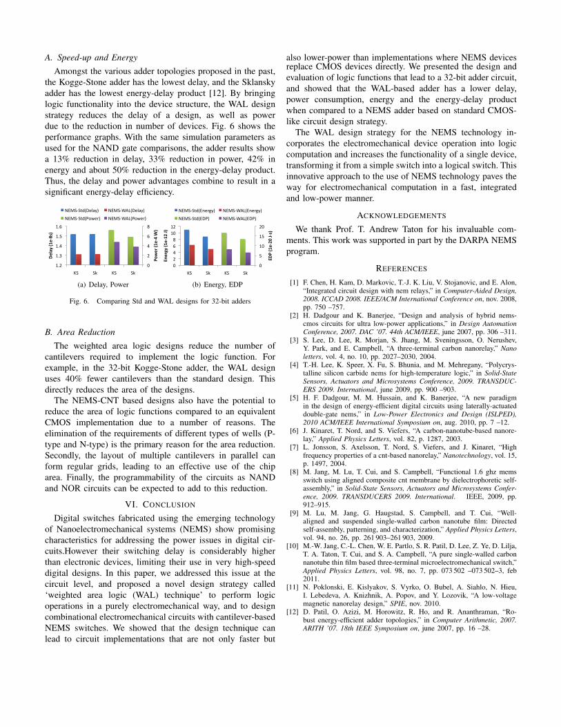
A. NAND/NOR Logic Gates
Using the weighted area concept, basic two-input logicfunctions of NAND and NOR can be directly implemented aselectromechanical designs. Fig. 4(a) shows the NAND designemploying NEMS-CNT devices using the standard MOSFETdesign technique. It is derived from CMOS-based implementa-tion of a NAND gate using only the switch-like behavior of thedevices. This design is expected to take advantage of the lowstatic power dissipation due to near-ideal OFF characteristicsof the devices, as well as the simplicity of fabrication dueto same type of devices performing the pull-up and pull-down function (as opposed to p-type and n-type required in
MOSFET designs). However, the maximum mechanical delayof the circuit for the worst-case input transition is two unitsof the mechanical delay of the cantilever beam.
! "
#$%
%&
!
"
#$%
%'
"(!) #$%(* "(!) "(!)(*
! + ,
(*
! !+ +,
!
+
+
,
!
"(!)
(*
#$%
(*
"(!)
! ,+
+-./0..1 +-./0..1 #2345678! ,+
+-./0..1 0../+-.1 #239490/!1
:;-
(a) NAND/NOR cir-cuit with Standard de-sign technique (4 can-tilevers). Each NEMSdevice corresponds toa MOSFET device ina CMOS-based NANDcircuit.
!"#!$%&!'()*+,*-.
!"#$%&'(&)"*+',-.#$%&)
!"#$%&'()*)(+&#,-.)/0!1')23/'4+)$&5/+,#2)(
6 7
89::
:
;
<= <>
89*?:@;A
/0 /1 2
!"# $## %&%'
$## !"# %()
*"+,-.,- %&%'/%()
012,3.4",56
B).'(/+CDEF+.'&,-('G'$/
!"
#"
$%%" &'%"
()!*#"
+," +-"
(b) NAND/NOR circuit withNEMS-WAL design (2 cantilevers)- Top view. Cantilevers C1 and C2have a weighted overlap area withgates A and B.
Fig. 4. NEMS-NAND designs
By employing the weighted logic design methodology, asmaller design with a delay as small as a single unit ofmechanical delay can be obtained. Fig. 4(b) shows a customdesign based on the weighted logic design concept that electro-mechanical forces can combine logically to enable switching.The two cantilevers C1 and C2 operate in parallel biased bypower and ground, and are controlled by common input linesA and B. With suitable overlap areas, forces from two gatescan either pull in a cantilever individually or in combination.Cantilever C1 experiences pull-in forces from the inputs andmakes contact with the output when both inputs are at Vdd.Cantilever C2 is constructed so that the overlap area betweenthe cantilever and each input is much larger than the overlaparea of cantilever C1 with each input. Its overlap area witheach gate is actually designed to ensure that each input isindividually capable of exerting a pull-in force that is sufficientto enable the cantilever to make contact with the output. Toincrease the gate-cantilever overlap area, the cantilever C2
can be designed as a ‘winged’ structure as shown in Fig.4(b). However, even with a simply designed cantilever, theNAND function can be obtained by separating the individualgates into individual cantilevers, as shown in Fig. 5(a). Withthe cantilevers biased at Vdd and Ground respectively, theNAND logic function is obtained. On the other hand whenthe cantilevers are biased at Ground and Vdd respectively, theNOR logic operation is obtained.
B. Simulation of NAND-WAL circuit
In order to verify the design, we simulated the NEMS-WALcircuit using the device model discussed in Section II-B withSPICE simulation tool. We extracted the sensitivity of theNAND-WAL design to varying values of the device param-

eters. With respect to ON-OFF time asymmetry, the NEMS-CNT devices consume lesser power in the WAL design, sincethe power dissipation in the short circuit mode when thedevices are switching at once (PSC) is reduced to almost zero.With respect to varying ON resistance and node capacitance,the WAL design did not show a lot of variation, however italways consumes lesser power and delay than the standardimplementation.
We also compared the NAND-WAL design with the stan-dard NAND (NAND-Std) design, using the following deviceparameters: Cnode = 1fF , Tmech = 1ns, VPI = 1V ,Ron = 1kΩ and Toff = 0.5Ton. These values were chosenas optimal or average parameters from the sensitivity curves.The load capacitance at the output nodes was assumed to be1fF . For all possible transitions in the NAND truth table, theWAL design reduces the maximum mechanical delay of twounits to a single unit, demonstrating the speed advantage ofincorporating logic capability within the device structure.
C. XOR gate
The XOR function is a key function that accomplishesthe SUM operation in a half-adder. Several interesting devicestructures have been proposed previously to implement theXOR function effectively in order to reduce the area of anadder, for example, the 4-terminal device structure in [1] andthe dual-gate structure in [5]. These structures were designedspecially for the XOR operation, and therefore would provemore effective. Under the weighted area logic scheme, theXOR gate (Fig. 5(c)) can be designed as four cantileversoperating in parallel and enabled by different gate inputs. Thisdemonstrates a regular pattern in which a NEMS-CNT circuitcan be designed and fabricated. It reduces the maximum delayof the function to two mechanical units.
!"#!$%&!'()*+,*-.
!"#$%&'(&)"*+',-.#$%&)
!"#$%&'()*)(+&#,-.)/0!1')23/'4+)$&5/+,#2)(
6 7
89::
:
;
<= <>
89*?:@;A
/0 /1 2
!"# $## %&%'
$## !"# %()
*"+,-.,- %&%'/%()
012,3.4",56
B).'(/+CDEF+.'&,-('G'$/
!"
#"
$" %" $"
&'!(#"
!"
#"
(a) Alternate NAND design
!"#!$%&!'()*+,*-.
!"#$%&'(&)"*+',-.#$%&)
!"#$%&'()*)(+&#,-.)/0!1')23/'4+)$&5/+,#2)(
6 7
89::
:
;
<= <>
89*?:@;A
/0 /1 2
!"# $## %&%'
$## !"# %()
*"+,-.,- %&%'/%()
012,3.4",56
B).'(/+CDEF+.'&,-('G'$/
!" #" !" #"
$%&'("
&"
("
(b) AND gate
!"
#"
$" %" $"
#" #"
!"
%"
&'!()*#"
!"
$" %" $"
#"
%"
+"
&'!,#-+"
(c) XOR gate
!"
#"
$" %" $"
#" #"
!"
%"
&'!()*#"
!"
$" %" $"
#"
%"
+"
&'!,#-+"
(d) Y=A+BC gate
Fig. 5. NEMS-WAL designs of adder components
D. Three input functions Y=A+B.C
In theory, the weighted area logic design can extend to anynumber of inputs. However, the practical limitations of anintegrated weighted logic design are determined by the number
of gates that can be fabricated for a single cantilever. Inpractice, an OR expression of the form Y = A+B+C+D+...can be accomplished with multiple cantilevers in parallel, asin the alternate NAND design (Fig. 5(a)).
The AND expressions of the form Y = A.B.C.D... aretrickier. The logic function Y = A + B.C offers goodinsights into implementing AND expressions. Fig. 5(d) showsa design that employs three gates driving a cantilever to-gether with different weights. The truth table of the functionY = A + B.C can be split into two parts, one part wheremaxterms M0 to M2 have the output 1 (Y1), and the otherpart where maxterms M3 through M7 have an output 0 (Y0).To implement Y0, two conditions must be satisfied: (1) theinput A must be capable of closing the switch individually;and (2) inputs B and C must be capable of pulling in thecantilever together. Thus, as shown in Fig. 5(d), the overlaparea of A with the cantilever biased at GND is designedto be large enough to establish the appropriate electrostaticattraction, while the overlap area is large and equally dividedbetween the inputs B and C. In the case of output of 1, theinput A must not pull-in the cantilever by itself, but incorporatethe force of B and/or C also. Therefore, the overlap area mustbe adjusted accordingly. If the overlap areas are specified interms of weights, where a weight of 1.0 indicates that theinput is capable of operating the cantilever by itself, then theweighted logic design of the function Y = A + B.C can berepresented as Y0 = A(1.0), B(0.5), C(0.5) for output of 0,and Y1 = A(0.75), B(0.25), C(0.25) for output of 1. Theoutput of this design is then applied to a NOT gate to obtainthe final output Y .
As the number of inputs in the AND term increases, thecantilever must be elongated for all inputs to be placed underthe same cantilever. Design rules for a practical gate haslimits of a minimum width, a minimum distance betweentwo gates, and length of cantilever. These limits determinethe number of inputs that can be implemented as an ANDterm. As fabrication challenges are addressed, it may becomepossible to have more than two gate inputs that actuate a singlecantilever beam, thus forming more compact designs.
V. PUTTING IT TOGETHER - 32-BIT ADDER DESIGN
The advantages derived from using a custom NEMS circuit,when compared to a non-custom circuit, increase as the logicfunction becomes complex. The three circuits discussed aboveform the basic circuits in an n-bit adder circuit. By composingthem into a 32-bit adder architecture, we can now quantify thespeed-up obtained by using the weighted area logic schemeover the standard technique of design. Fig. 5 shows the designsfor the base circuits of the adder. The AND gate (Fig. 5(b))is designed as the previously described NAND gate followedby an inverter. The mechanical delay of this gate is two units– one unit due to the NAND gate and the second due to theNOT gate.
A. Speed-up and Energy
Amongst the various adder topologies proposed in the past,the Kogge-Stone adder has the lowest delay, and the Sklanskyadder has the lowest energy-delay product [12]. By bringinglogic functionality into the device structure, the WAL designstrategy reduces the delay of a design, as well as powerdue to the reduction in number of devices. Fig. 6 shows theperformance graphs. With the same simulation parameters asused for the NAND gate comparisons, the adder results showa 13% reduction in delay, 33% reduction in power, 42% inenergy and about 50% reduction in the energy-delay product.Thus, the delay and power advantages combine to result in asignificant energy-delay efficiency.
!" #$%&$'( )%*&(&
(+
,+
&+
)+
-+
#%,+
#%$+
#%&+
#%*+
#%)+
.!+ !"+ .!+ !"+
!"#$%&'($)*&+
,&
-$./0&'($)12,&
/01!2!3456789:;+ /01!2<=>56789:;+
/01!2!345?@A7B;+ /01!2<=>5?@A7B;+
(+
*+
#(+
#*+
,(+
(+
,+
&+
)+
-+
#(+
#,+
.!+ !"+ .!+ !"+
3-!&'($)45&6)2,&
37$%80&'($)(4&6,&
/01!2!3450C7BD:;+ /01!2<=>50C7BD:;+
/01!2!34506?;+ /01!2<=>506?;+
(a) Delay, Power
!" #$%&$'( )%*&(&
(+
,+
&+
)+
-+
#%,+
#%$+
#%&+
#%*+
#%)+
.!+ !"+ .!+ !"+
!"#$%&'($)*&+
,&
-$./0&'($)12,&
/01!2!3456789:;+ /01!2<=>56789:;+
/01!2!345?@A7B;+ /01!2<=>5?@A7B;+
(+
*+
#(+
#*+
,(+
(+
,+
&+
)+
-+
#(+
#,+
.!+ !"+ .!+ !"+3-!&'($)45&6)2,&
37$%80&'($)(4&6,&
/01!2!3450C7BD:;+ /01!2<=>50C7BD:;+
/01!2!34506?;+ /01!2<=>506?;+
(b) Energy, EDP
Fig. 6. Comparing Std and WAL designs for 32-bit adders
B. Area Reduction
The weighted area logic designs reduce the number ofcantilevers required to implement the logic function. Forexample, in the 32-bit Kogge-Stone adder, the WAL designuses 40% fewer cantilevers than the standard design. Thisdirectly reduces the area of the designs.
The NEMS-CNT based designs also have the potential toreduce the area of logic functions compared to an equivalentCMOS implementation due to a number of reasons. Theelimination of the requirements of different types of wells (P-type and N-type) is the primary reason for the area reduction.Secondly, the layout of multiple cantilevers in parallel canform regular grids, leading to an effective use of the chiparea. Finally, the programmability of the circuits as NANDand NOR circuits can be expected to add to this reduction.
VI. CONCLUSION
Digital switches fabricated using the emerging technologyof Nanoelectromechanical systems (NEMS) show promisingcharacteristics for addressing the power issues in digital cir-cuits.However their switching delay is considerably higherthan electronic devices, limiting their use in very high-speeddigital designs. In this paper, we addressed this issue at thecircuit level, and proposed a novel design strategy called‘weighted area logic (WAL) technique’ to perform logicoperations in a purely electromechanical way, and to designcombinational electromechanical circuits with cantilever-basedNEMS switches. We showed that the design technique canlead to circuit implementations that are not only faster but
also lower-power than implementations where NEMS devicesreplace CMOS devices directly. We presented the design andevaluation of logic functions that lead to a 32-bit adder circuit,and showed that the WAL-based adder has a lower delay,power consumption, energy and the energy-delay productwhen compared to a NEMS adder based on standard CMOS-like circuit design strategy.
The WAL design strategy for the NEMS technology in-corporates the electromechanical device operation into logiccomputation and increases the functionality of a single device,transforming it from a simple switch into a logical switch. Thisinnovative approach to the use of NEMS technology paves theway for electromechanical computation in a fast, integratedand low-power manner.
ACKNOWLEDGEMENTS
We thank Prof. T. Andrew Taton for his invaluable com-ments. This work was supported in part by the DARPA NEMSprogram.
REFERENCES
[1] F. Chen, H. Kam, D. Markovic, T.-J. K. Liu, V. Stojanovic, and E. Alon,“Integrated circuit design with nem relays,” in Computer-Aided Design,2008. ICCAD 2008. IEEE/ACM International Conference on, nov. 2008,pp. 750 –757.
[2] H. Dadgour and K. Banerjee, “Design and analysis of hybrid nems-cmos circuits for ultra low-power applications,” in Design AutomationConference, 2007. DAC ’07. 44th ACM/IEEE, june 2007, pp. 306 –311.
[3] S. Lee, D. Lee, R. Morjan, S. Jhang, M. Sveningsson, O. Nerushev,Y. Park, and E. Campbell, “A three-terminal carbon nanorelay,” Nanoletters, vol. 4, no. 10, pp. 2027–2030, 2004.
[4] T.-H. Lee, K. Speer, X. Fu, S. Bhunia, and M. Mehregany, “Polycrys-talline silicon carbide nems for high-temperature logic,” in Solid-StateSensors, Actuators and Microsystems Conference, 2009. TRANSDUC-ERS 2009. International, june 2009, pp. 900 –903.
[5] H. F. Dadgour, M. M. Hussain, and K. Banerjee, “A new paradigmin the design of energy-efficient digital circuits using laterally-actuateddouble-gate nems,” in Low-Power Electronics and Design (ISLPED),2010 ACM/IEEE International Symposium on, aug. 2010, pp. 7 –12.
[6] J. Kinaret, T. Nord, and S. Viefers, “A carbon-nanotube-based nanore-lay,” Applied Physics Letters, vol. 82, p. 1287, 2003.
[7] L. Jonsson, S. Axelsson, T. Nord, S. Viefers, and J. Kinaret, “Highfrequency properties of a cnt-based nanorelay,” Nanotechnology, vol. 15,p. 1497, 2004.
[8] M. Jang, M. Lu, T. Cui, and S. Campbell, “Functional 1.6 ghz memsswitch using aligned composite cnt membrane by dielectrophoretic self-assembly,” in Solid-State Sensors, Actuators and Microsystems Confer-ence, 2009. TRANSDUCERS 2009. International. IEEE, 2009, pp.912–915.
[9] M. Lu, M. Jang, G. Haugstad, S. Campbell, and T. Cui, “Well-aligned and suspended single-walled carbon nanotube film: Directedself-assembly, patterning, and characterization,” Applied Physics Letters,vol. 94, no. 26, pp. 261 903–261 903, 2009.
[10] M.-W. Jang, C.-L. Chen, W. E. Partlo, S. R. Patil, D. Lee, Z. Ye, D. Lilja,T. A. Taton, T. Cui, and S. A. Campbell, “A pure single-walled carbonnanotube thin film based three-terminal microelectromechanical switch,”Applied Physics Letters, vol. 98, no. 7, pp. 073 502 –073 502–3, feb2011.
[11] N. Poklonski, E. Kislyakov, S. Vyrko, O. Bubel, A. Siahlo, N. Hieu,I. Lebedeva, A. Knizhnik, A. Popov, and Y. Lozovik, “A low-voltagemagnetic nanorelay design,” SPIE, nov. 2010.
[12] D. Patil, O. Azizi, M. Horowitz, R. Ho, and R. Ananthraman, “Ro-bust energy-efficient adder topologies,” in Computer Arithmetic, 2007.ARITH ’07. 18th IEEE Symposium on, june 2007, pp. 16 –28.