week 9: chap.13 other semiconductor material
TRANSCRIPT
Week 9: Chap.13 Other Semiconductor Material
© DJMorrissey, 2o19
Germanium Diodes
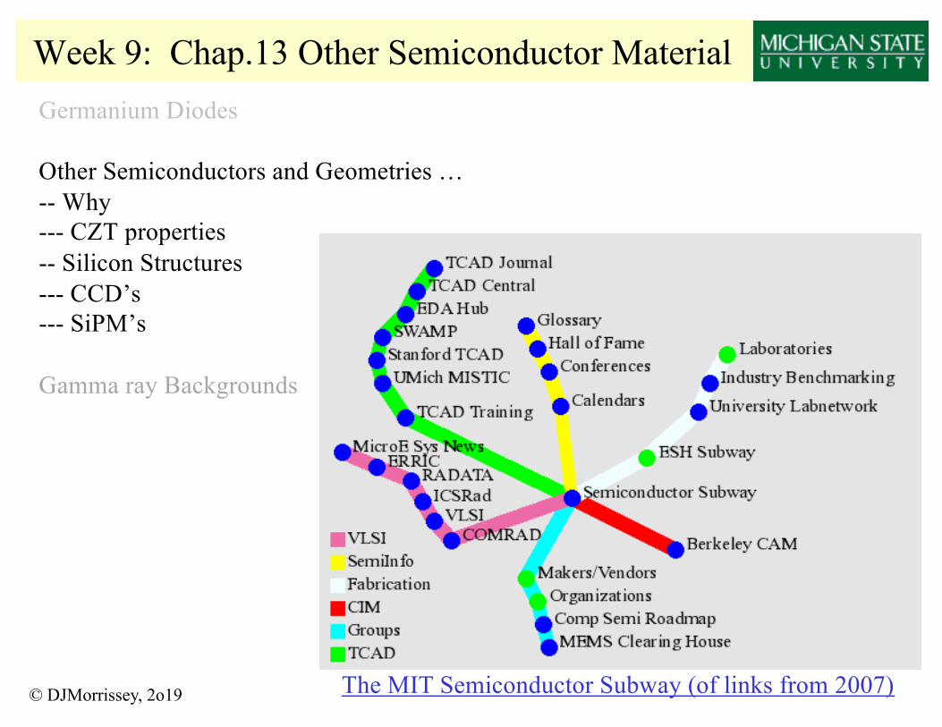
Other Semiconductors and Geometries …-- Why--- CZT properties-- Silicon Structures--- CCD’s--- SiPM’s
Gamma ray Backgrounds
The MIT Semiconductor Subway (of links from 2007)
© DJMorrissey, 2o19
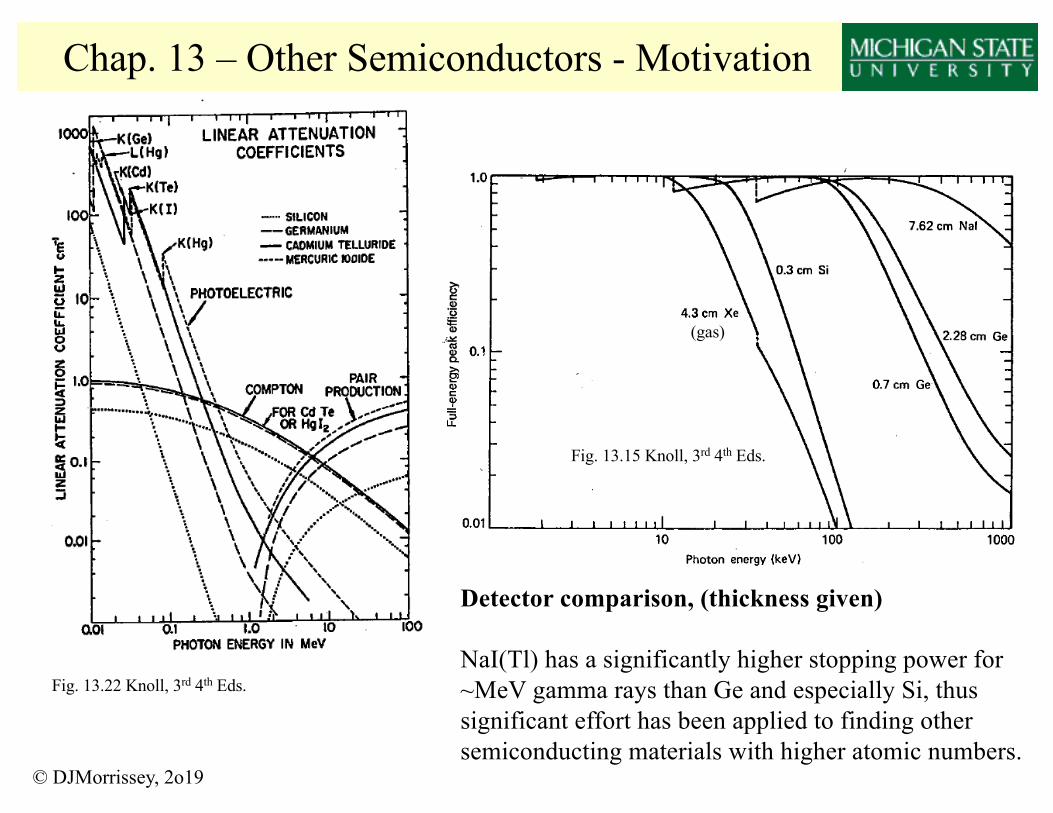
Chap. 13 – Other Semiconductors - Motivation
Fig. 13.15 Knoll, 3rd 4th Eds.
Detector comparison, (thickness given)
NaI(Tl) has a significantly higher stopping power for ~MeV gamma rays than Ge and especially Si, thus significant effort has been applied to finding other semiconducting materials with higher atomic numbers.
Fig. 13.22 Knoll, 3rd 4th Eds.
(gas)

© DJMorrissey, 2o19
Other Semiconductor Properties
C.A.Klein, J.App. Phys. 39 (1968) 2029
Fig. 13.21 Knoll, 3rd 4th Eds.
NaI(Tl) 11-53-81 5.8 – 6.3 ( 0 , 0 scintillator) 3.7 [ NaI from Poole, et al. Chem.Phys.Lett.26 (1974) 514 ]
Recall correlation of W with band gap – higher W leads to lower signal but also lower thermal noise.
5.81350 120

© DJMorrissey, 2o19
Other Semiconductors – CZT
Typical sensitivity of integrated device: 0.1 mRem/hr to 1 Rem/hr
Q: How much power is this in a 10x10x0.5 mm3 crystal?[max: 5.0 GeV/s ]
1 cm
1 in
M.Spahn, NIM A731 (2013) 57
Similar to Knoll’s 13.44
© DJMorrissey, 2o19
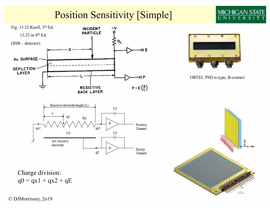
Position Sensitivity [Simple]Fig. 13.32 Knoll, 3rd Ed.
13.33 in 4th Ed.
(SSB – detector)
ORTEC PSD n-type, B-contact
Charge division: q0 = qx1 + qx2 + qE
© DJMorrissey, 2o19
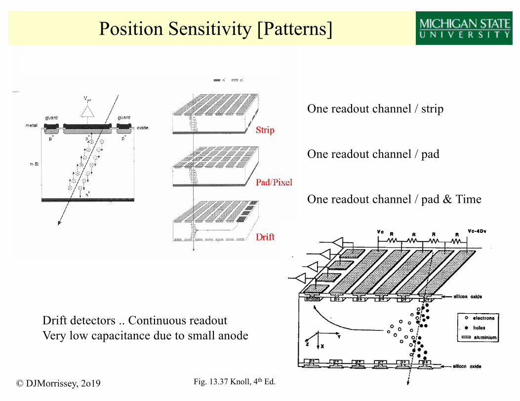
Position Sensitivity [Patterns]
Fig. 13.36 Knoll, 3rd Ed.
Drift detectors .. Continuous readout Very low capacitance due to small anode
One readout channel / strip
One readout channel / pad
One readout channel / pad & Time
Fig. 13.37 Knoll, 4th Ed.
© DJMorrissey, 2o19
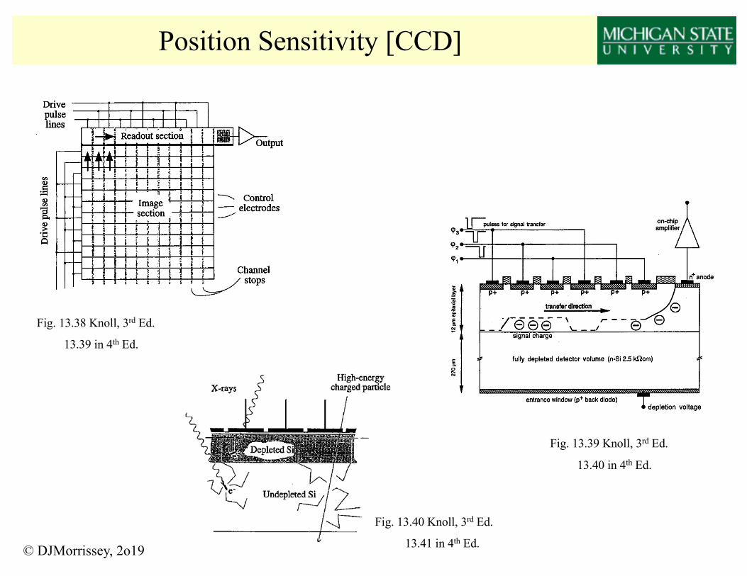
Position Sensitivity [CCD]
Fig. 13.38 Knoll, 3rd Ed.
13.39 in 4th Ed.
Fig. 13.39 Knoll, 3rd Ed.
13.40 in 4th Ed.
Fig. 13.40 Knoll, 3rd Ed.
13.41 in 4th Ed.

New Application – SiPM
© DJMorrissey, 2o19
(1) Recall that NaI(Tl) and other scintillators emit ~tens of thousand photons per MeV deposited in the crystal and of order ½ make to the photocathode and then¼ create photoelectrons. Thus, one has ~thousands information carriers per MeV à few % resolution.
(2) A Silicon diode will “break down” or discharge if it is over biased. If the discharge can be terminated then only a large pulse is passed. Such a device that breaks down when exposed to light: avalanche photodiode (APD).
(3) Extremely small structures (circuits) can be created in silicon, e.g., thousands
Fig.9.1 Knoll, 3rd,4th Eds.
Hamamatsu SiPMSensL Documentation
KETEK SiPM
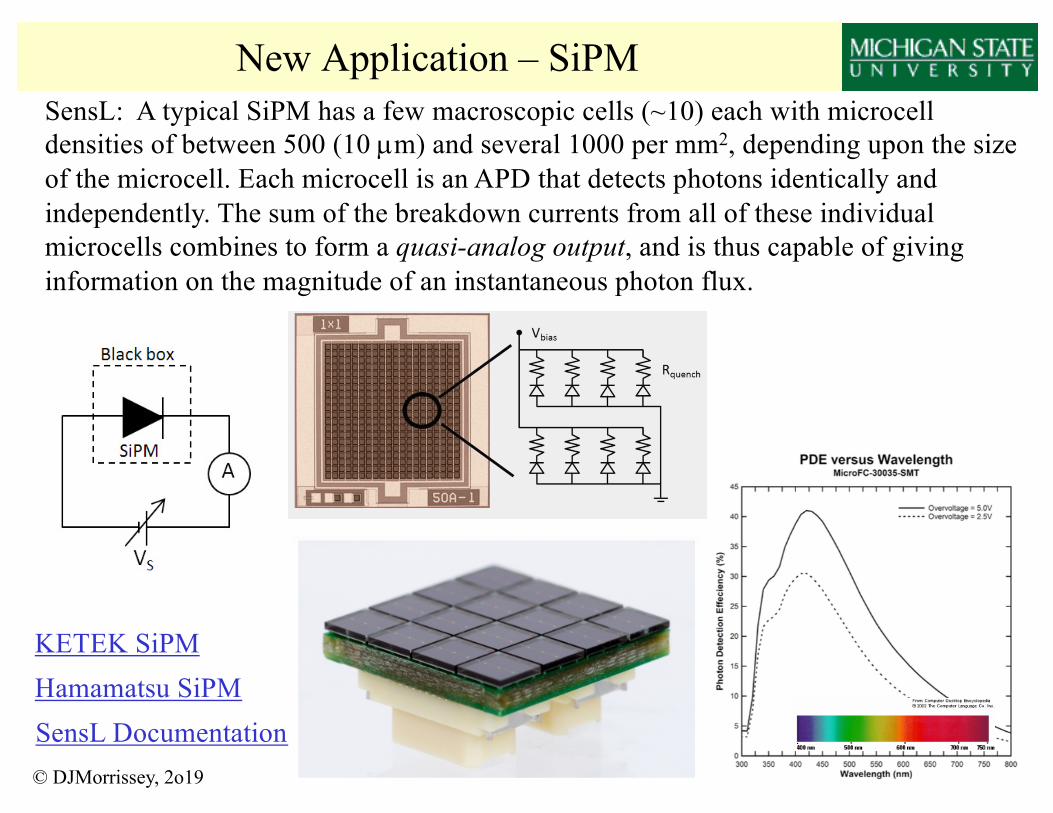
New Application – SiPM
© DJMorrissey, 2o19
SensL: A typical SiPM has a few macroscopic cells (~10) each with microcell densities of between 500 (10 µm) and several 1000 per mm2, depending upon the size of the microcell. Each microcell is an APD that detects photons identically and independently. The sum of the breakdown currents from all of these individual microcells combines to form a quasi-analog output, and is thus capable of giving information on the magnitude of an instantaneous photon flux.
Hamamatsu SiPMSensL Documentation
KETEK SiPM
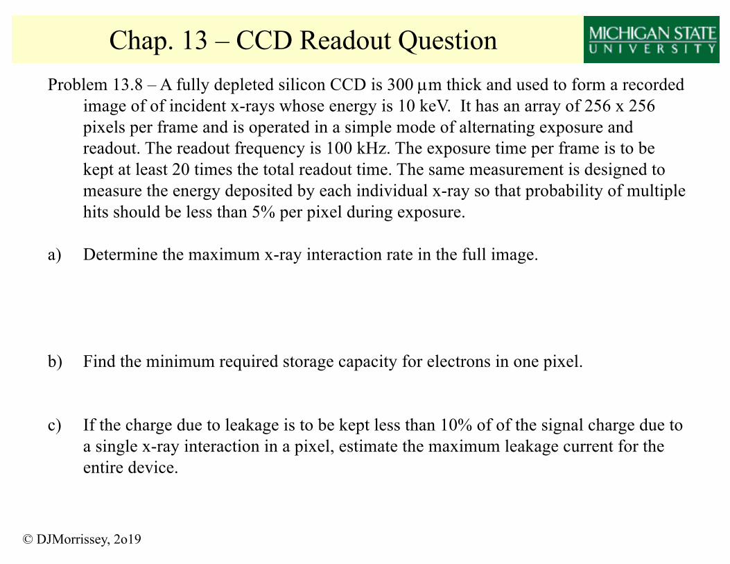
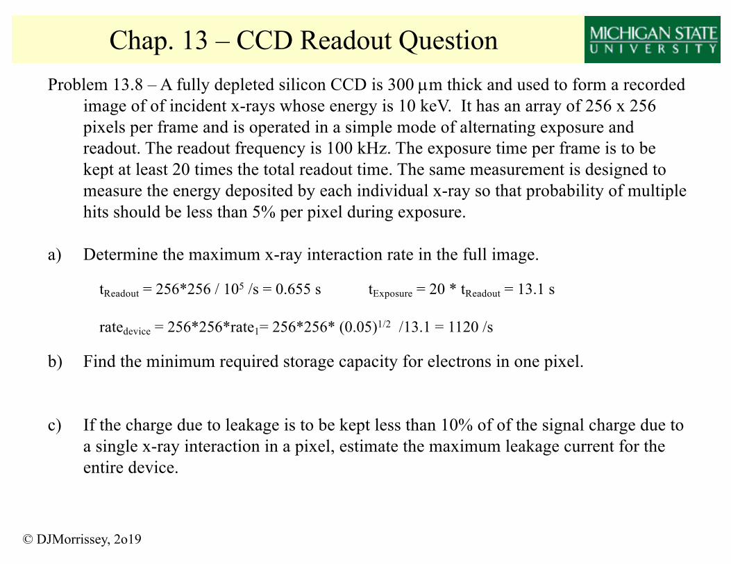
Problem 13.8 – A fully depleted silicon CCD is 300 µm thick and used to form a recorded image of of incident x-rays whose energy is 10 keV. It has an array of 256 x 256 pixels per frame and is operated in a simple mode of alternating exposure and readout. The readout frequency is 100 kHz. The exposure time per frame is to be kept at least 20 times the total readout time. The same measurement is designed to measure the energy deposited by each individual x-ray so that probability of multiple hits should be less than 5% per pixel during exposure.
a) Determine the maximum x-ray interaction rate in the full image.
b) Find the minimum required storage capacity for electrons in one pixel.
c) If the charge due to leakage is to be kept less than 10% of of the signal charge due to a single x-ray interaction in a pixel, estimate the maximum leakage current for the entire device.
© DJMorrissey, 2o19
Chap. 13 – CCD Readout Question
tReadout = 256*256 / 105 /s = 0.655 s tExposure = 20 * tReadout = 13.1 sOne pixel: Knoll’s answer P = 0.05 = rate1 * texposure .. 5% chance one gets hit ..
ratedevice = 256*256*rate1= 256*256*0.05/13.1 = 250/s

Problem 13.8 – A fully depleted silicon CCD is 300 µm thick and used to form a recorded image of of incident x-rays whose energy is 10 keV. It has an array of 256 x 256 pixels per frame and is operated in a simple mode of alternating exposure and readout. The readout frequency is 100 kHz. The exposure time per frame is to be kept at least 20 times the total readout time. The same measurement is designed to measure the energy deposited by each individual x-ray so that probability of multiple hits should be less than 5% per pixel during exposure.
a) Determine the maximum x-ray interaction rate in the full image.
© DJMorrissey, 2o19
Chap. 13 – CCD Readout Question
tReadout = 256*256 / 105 /s = 0.655 s tExposure = 20 * tReadout = 13.1 s
5% chance of more than one per pixel ..
P(0) = e-rt
P(1) = rt e-rt
P(>1) = 1 – [P(0)+P(1)] = 1 - rt e-rt - e-rt = 1 - e-rt (rt + 1) 0.05 = 1 - e-rt (rt + 1)e-rt (rt + 1) = 0.95 e-x ~ 1 – x + … for small x(1 – rt ) (rt + 1) = 0.95 1 – (rt)2 = 0.95 à rt = (0.05)1/2 à r1 = (0.05)1/2 /t
ratedevice = 256*256*rate1= 256*256* (0.05)1/2 /13.1 = 1120 /s
Problem 13.8 – A fully depleted silicon CCD is 300 µm thick and used to form a recorded image of of incident x-rays whose energy is 10 keV. It has an array of 256 x 256 pixels per frame and is operated in a simple mode of alternating exposure and readout. The readout frequency is 100 kHz. The exposure time per frame is to be kept at least 20 times the total readout time. The same measurement is designed to measure the energy deposited by each individual x-ray so that probability of multiple hits should be less than 5% per pixel during exposure.
a) Determine the maximum x-ray interaction rate in the full image.
b) Find the minimum required storage capacity for electrons in one pixel.
c) If the charge due to leakage is to be kept less than 10% of of the signal charge due to a single x-ray interaction in a pixel, estimate the maximum leakage current for the entire device.
© DJMorrissey, 2o19
Chap. 13 – CCD Readout Question
Ne = E/W = 10,000 eV / 3.65eV/IP = 2728 IP’s
Ne = 0.1 * 2728 e/pixel * 256 * 256 pixels/frame = 1.8x10⁷ eI = Ne *1.602x10⁻¹⁹ C/electron / 13.1 s = 2.2x10⁻¹³ A
tReadout = 256*256 / 105 /s = 0.655 s tExposure = 20 * tReadout = 13.1 s
ratedevice = 256*256*rate1= 256*256* (0.05)1/2 /13.1 = 1120 /s