week 6 the 8088 and 8086 microprocessors and their memory...
TRANSCRIPT
Week 6
The 8088 and 8086 Microprocessors and Their Memory and Input/Output
Interfaces

2
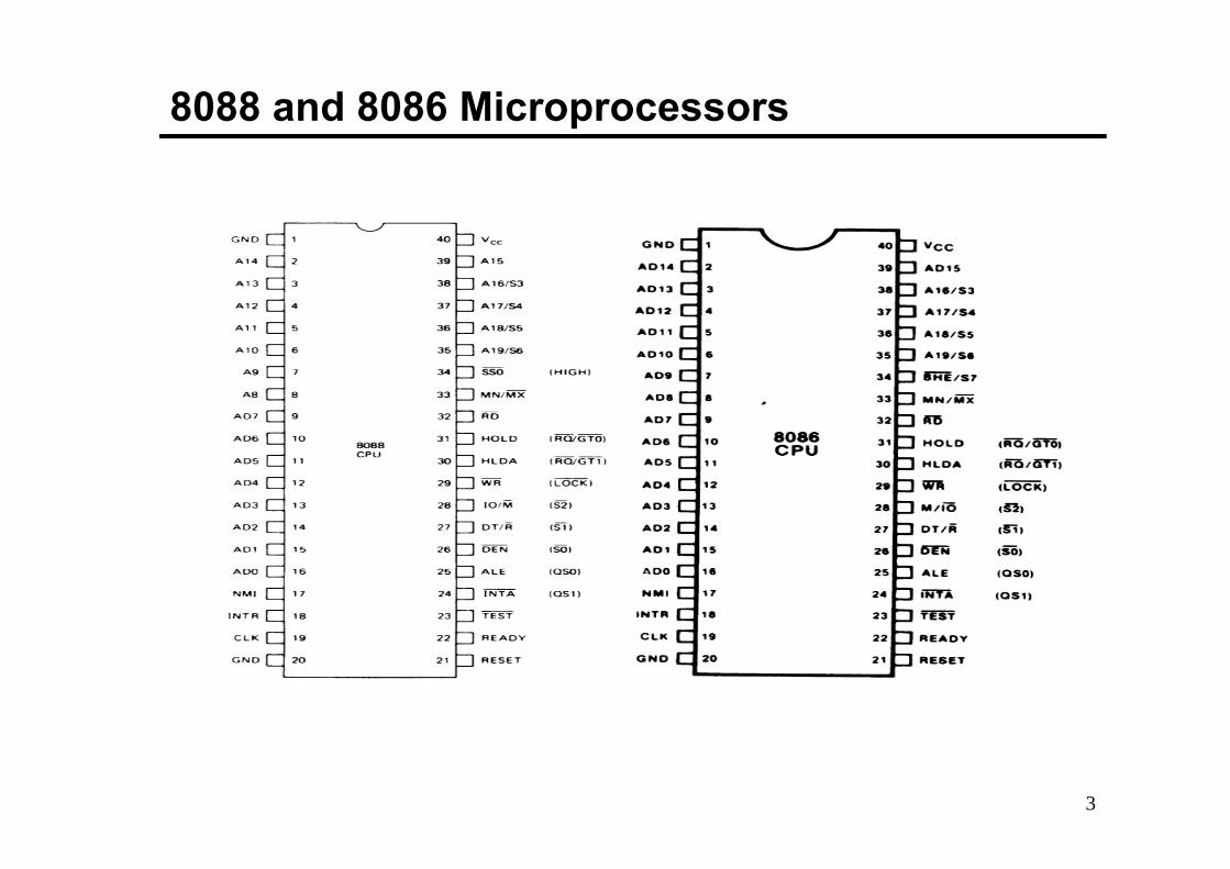
8086 and 8088 Microprocessors
• 8086 announced in 1978; 8086 is a 16 bit microprocessor with a 16 bit data bus
• 8088 announced in 1979; 8088 is a 16 bit microprocessor with an 8 bit data bus
• Both manufactured using High-performance Metal Oxide Semiconductor (HMOS) technology
• Both contain about 29000 transistors
• Both are packaged in 40 pin dual-in-line package (DIP)
• Address lines A0-A7 and Data lines D0-D7 are multiplexed in 8088 – By multiplexed we mean that the same pysical pin carries an address bit
at one time and the data bit another time
• Address lines A0-A15 and Data lines D0-D15 are multiplexed in 8086
3
8088 and 8086 Microprocessors

4
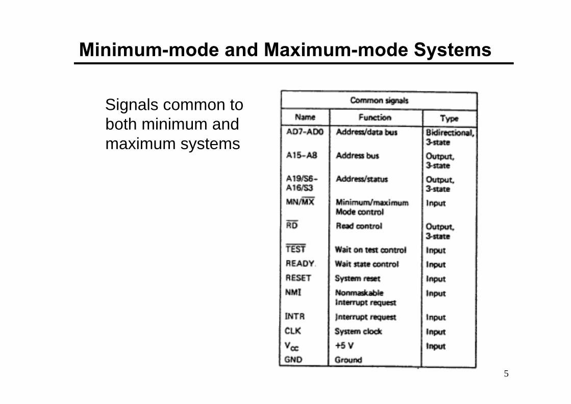
Minimum-mode and Maximum-mode Systems
• 8088 and 8086 microprocessors can be configured to work in either of the two modes: the minimum mode and the maximum mode
• Minimum mode:– Pull MN/MX to logic 1
– Typically smaller systems and contains a single microprocessor
• Maximum mode– Pull MN/MX logic 0
– Larger systems with more than one processor
5
Minimum-mode and Maximum-mode Systems
Signals common to both minimum and maximum systems
6
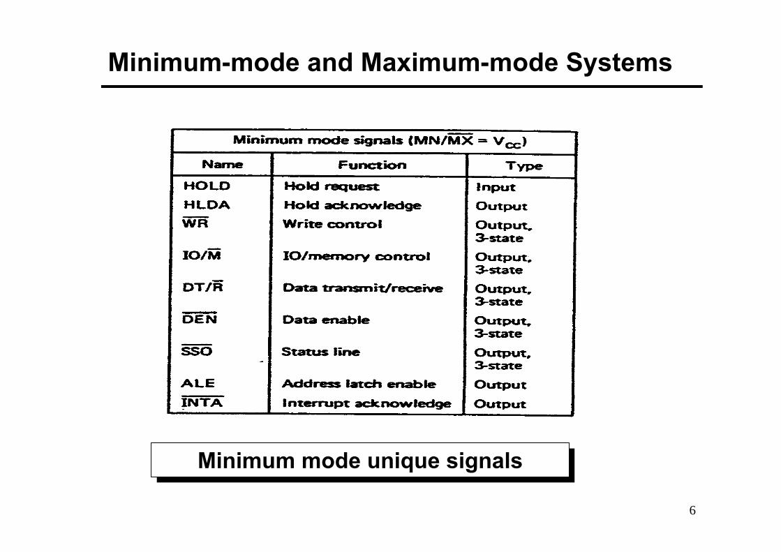
Minimum-mode and Maximum-mode Systems
Minimum mode unique signals
7
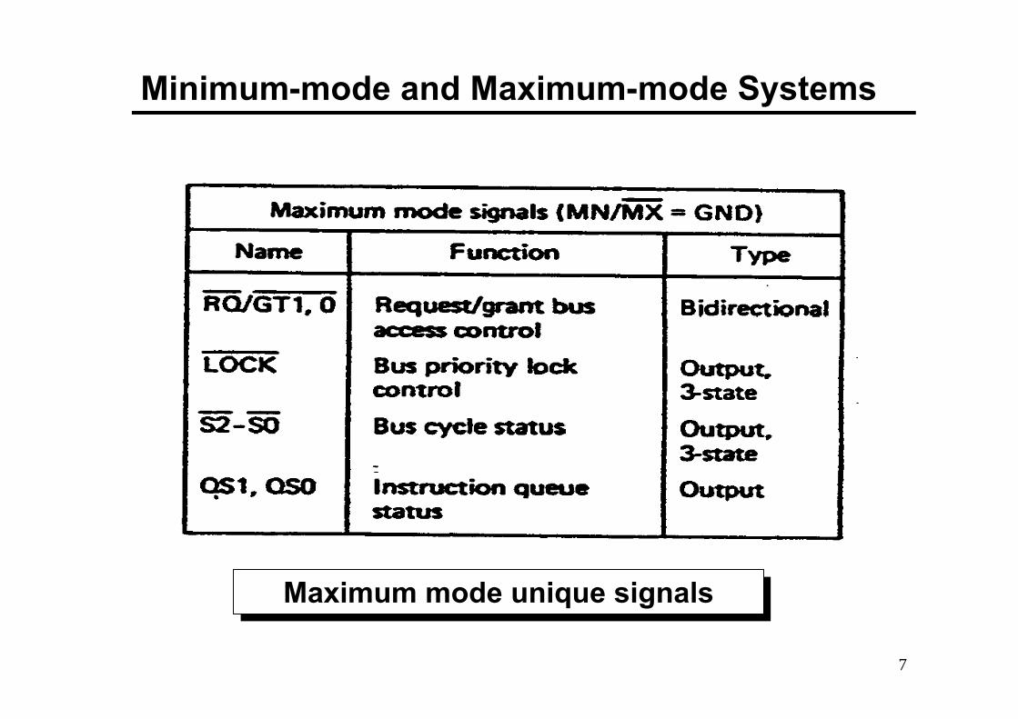
Minimum-mode and Maximum-mode Systems
Maximum mode unique signals

8
8088 Minimum-mode block diagram
9
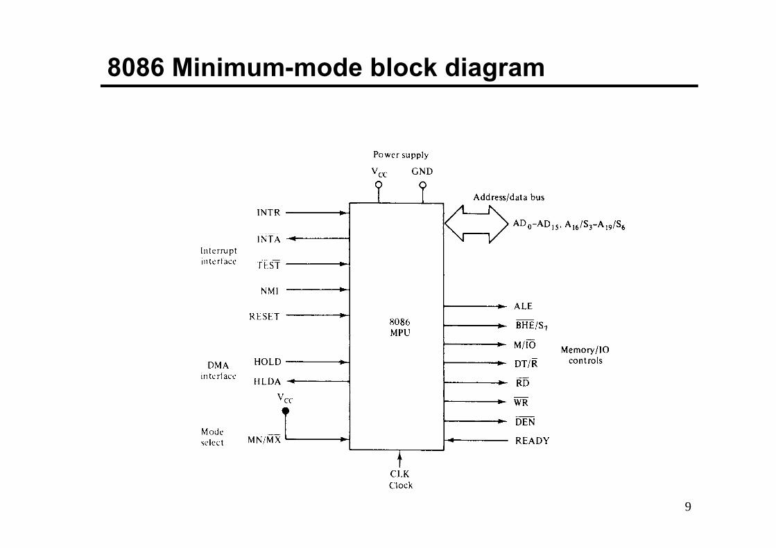
8086 Minimum-mode block diagram
10
Minimum Mode Interface
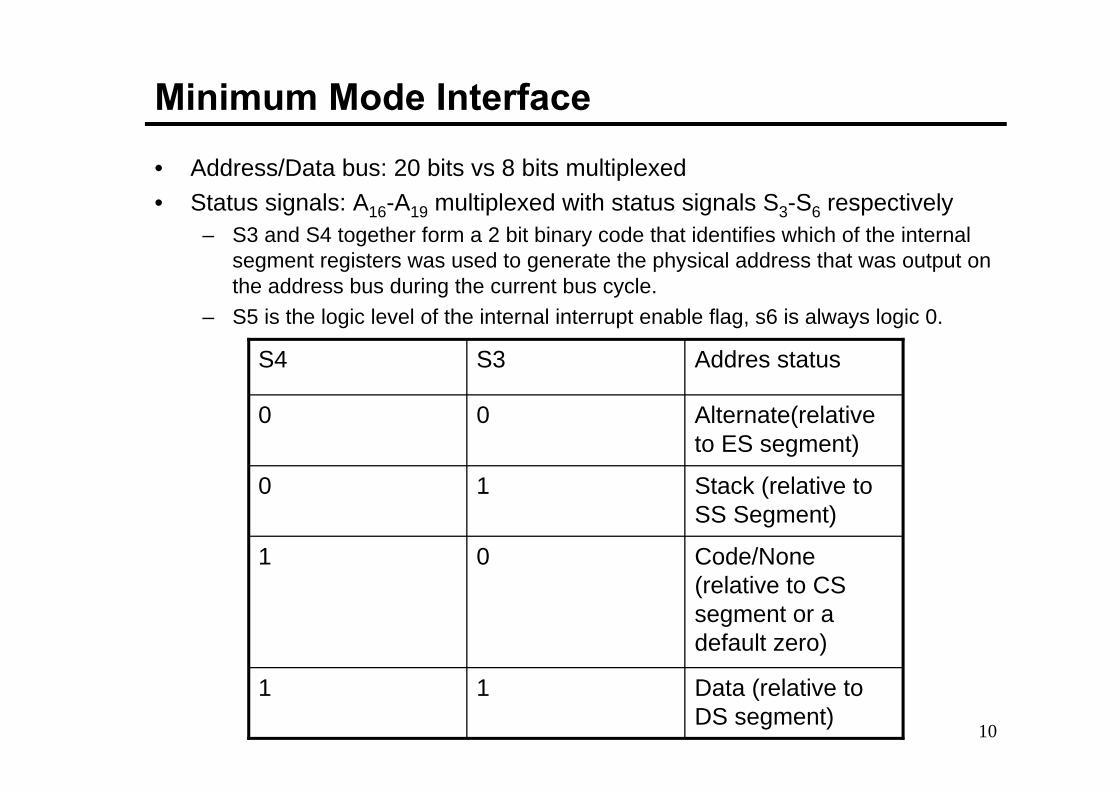
• Address/Data bus: 20 bits vs 8 bits multiplexed
• Status signals: A16-A19 multiplexed with status signals S3-S6 respectively– S3 and S4 together form a 2 bit binary code that identifies which of the internal
segment registers was used to generate the physical address that was output on the address bus during the current bus cycle.
– S5 is the logic level of the internal interrupt enable flag, s6 is always logic 0.
Data (relative to DS segment)
11
Code/None (relative to CS segment or a default zero)
01
Stack (relative to SS Segment)
10
Alternate(relative to ES segment)
00
Addres statusS3S4
11
Minimum Mode Interface
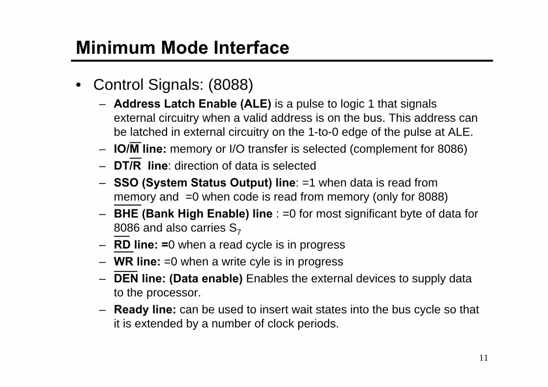
• Control Signals: (8088) – Address Latch Enable (ALE) is a pulse to logic 1 that signals
external circuitry when a valid address is on the bus. This address can be latched in external circuitry on the 1-to-0 edge of the pulse at ALE.
– IO/M line: memory or I/O transfer is selected (complement for 8086)
– DT/R line: direction of data is selected
– SSO (System Status Output) line: =1 when data is read from memory and =0 when code is read from memory (only for 8088)
– BHE (Bank High Enable) line : =0 for most significant byte of data for 8086 and also carries S7
– RD line: =0 when a read cycle is in progress
– WR line: =0 when a write cyle is in progress
– DEN line: (Data enable) Enables the external devices to supply data to the processor.
– Ready line: can be used to insert wait states into the bus cycle so that it is extended by a number of clock periods.

12
Minimum Mode Interface
• Interrupt signals:– INTR (Interrupt request) :=1 shows there is a service
request, sampled at the final clock cycle of each instruction acquisition cycle.
– INTA : Processor responds with two pulses going to 0 when it services the interrupt and waits for the interrupt service number after the second pulse.
– TEST: Processor suspends operation when =1. Resumes operation when=0. Used to syncronize the processor to external events.
– NMI (Nonmaskable interrupt) : A leading edge transition causes the processor go to the interrupt routine after the current instruction is executed.
– RESET : =0 Starts the reset sequence.

13
Minimum Mode Interface
• DMA (Direct Memory Access) Interface Signals:– HOLD : External device puts logic level 1 to HOLD
input to take control of the bus for DMA request.
– HLDA (Hold acknowledge) : Processor responds by putting logic level 1 to HDLA.
– In this state; Address and Data lines, SSO, IO/M, DT/R, RD, WR, DEN signals are all put to high-Z state.
14
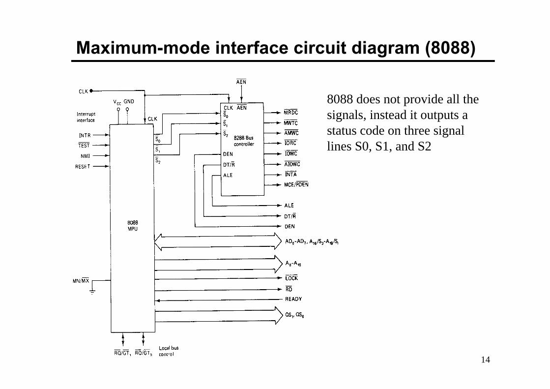
Maximum-mode interface circuit diagram (8088)
8088 does not provide all the signals, instead it outputs a status code on three signal lines S0, S1, and S2
15
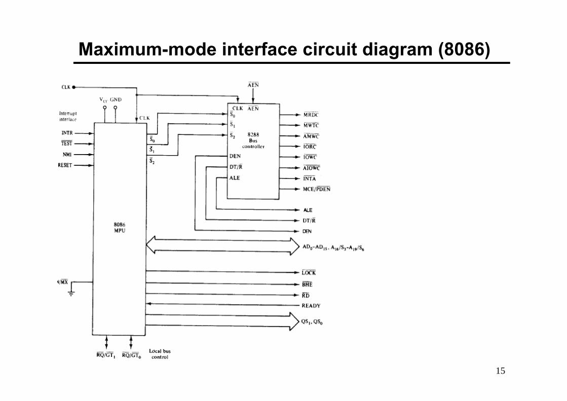
Maximum-mode interface circuit diagram (8086)
16
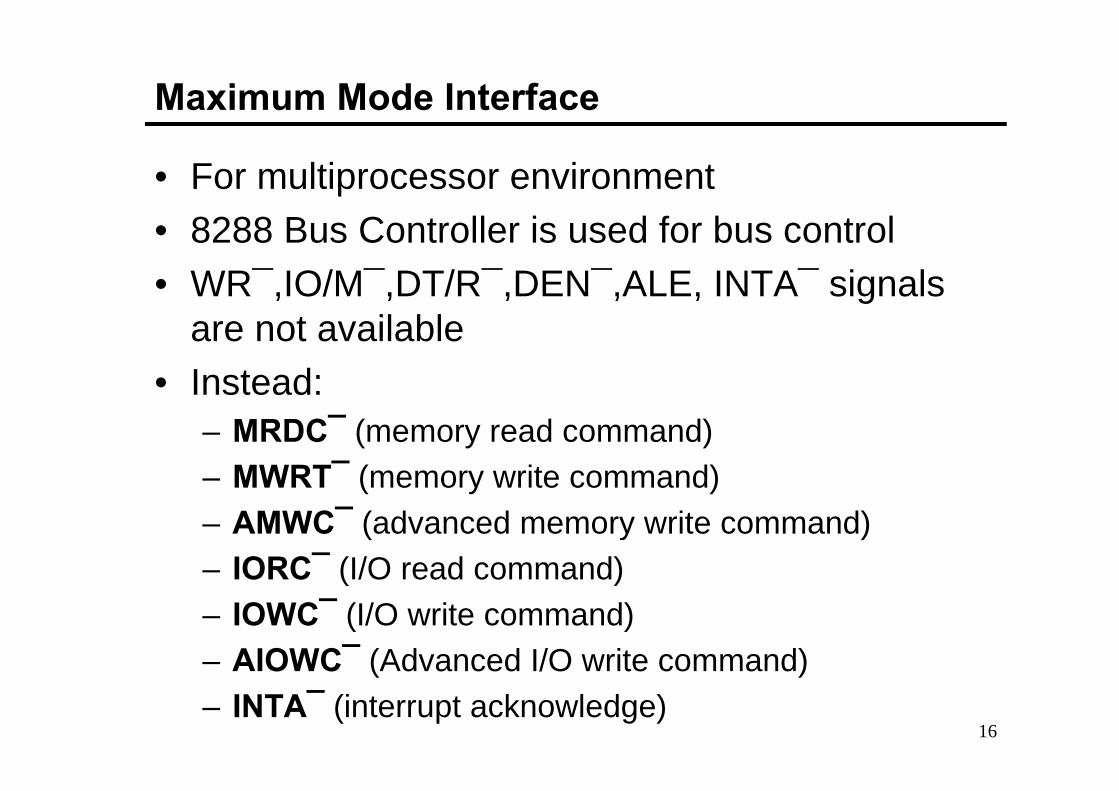
Maximum Mode Interface
• For multiprocessor environment
• 8288 Bus Controller is used for bus control
• WR¯,IO/M¯,DT/R¯,DEN¯,ALE, INTA¯ signals are not available
• Instead:– MRDC¯ (memory read command)
– MWRT¯ (memory write command)
– AMWC¯ (advanced memory write command)
– IORC¯ (I/O read command)
– IOWC¯ (I/O write command)
– AIOWC¯ (Advanced I/O write command)
– INTA¯ (interrupt acknowledge)
17
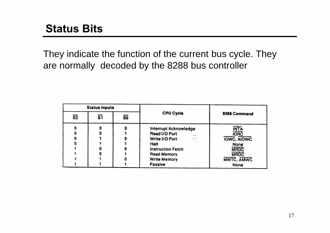
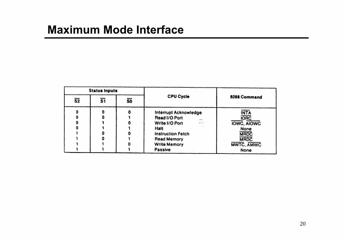
Status Bits
They indicate the function of the current bus cycle. They are normally decoded by the 8288 bus controller
18
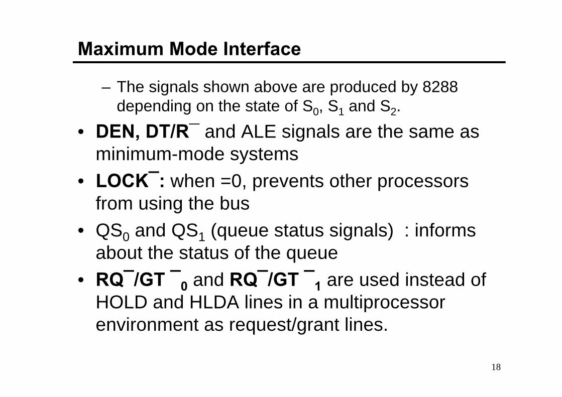
Maximum Mode Interface
– The signals shown above are produced by 8288 depending on the state of S0, S1 and S2.
• DEN, DT/R¯ and ALE signals are the same as minimum-mode systems
• LOCK¯: when =0, prevents other processors from using the bus
• QS0 and QS1 (queue status signals) : informs about the status of the queue
• RQ¯/GT ¯0 and RQ¯/GT ¯1 are used instead of HOLD and HLDA lines in a multiprocessor environment as request/grant lines.
19
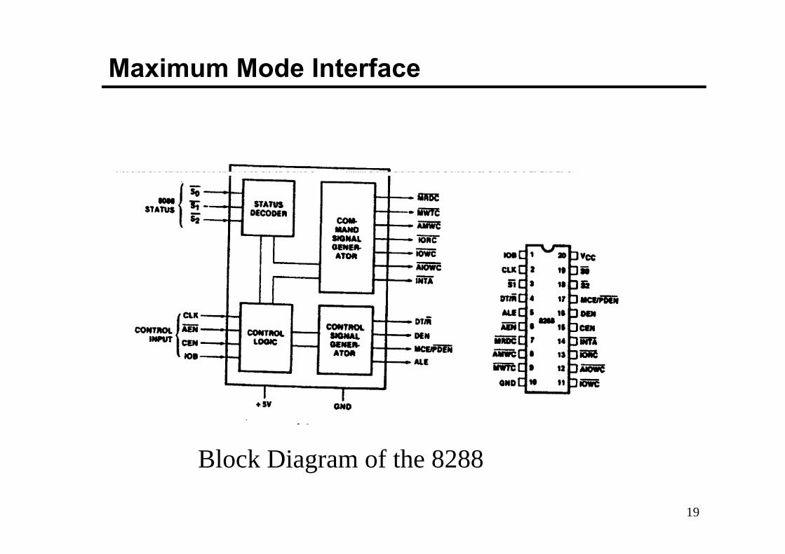
Maximum Mode Interface
Block Diagram of the 8288
20
Maximum Mode Interface
21
Bus Cycle and Time States
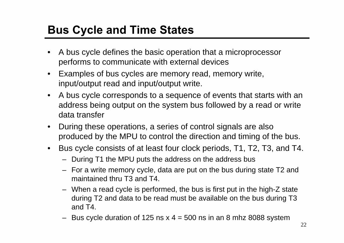
22
Bus Cycle and Time States
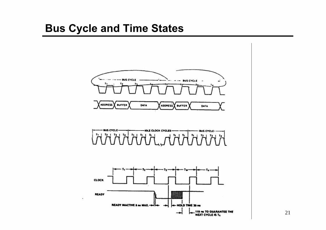
• A bus cycle defines the basic operation that a microprocessor performs to communicate with external devices
• Examples of bus cycles are memory read, memory write, input/output read and input/output write.
• A bus cycle corresponds to a sequence of events that starts with an address being output on the system bus followed by a read or write data transfer
• During these operations, a series of control signals are also produced by the MPU to control the direction and timing of the bus.
• Bus cycle consists of at least four clock periods, T1, T2, T3, and T4. – During T1 the MPU puts the address on the address bus
– For a write memory cycle, data are put on the bus during state T2 and maintained thru T3 and T4.
– When a read cycle is performed, the bus is first put in the high-Z state during T2 and data to be read must be available on the bus during T3 and T4.
– Bus cycle duration of 125 ns x 4 = 500 ns in an 8 mhz 8088 system

23
24
25

26
Read Cycle of the 8088
27
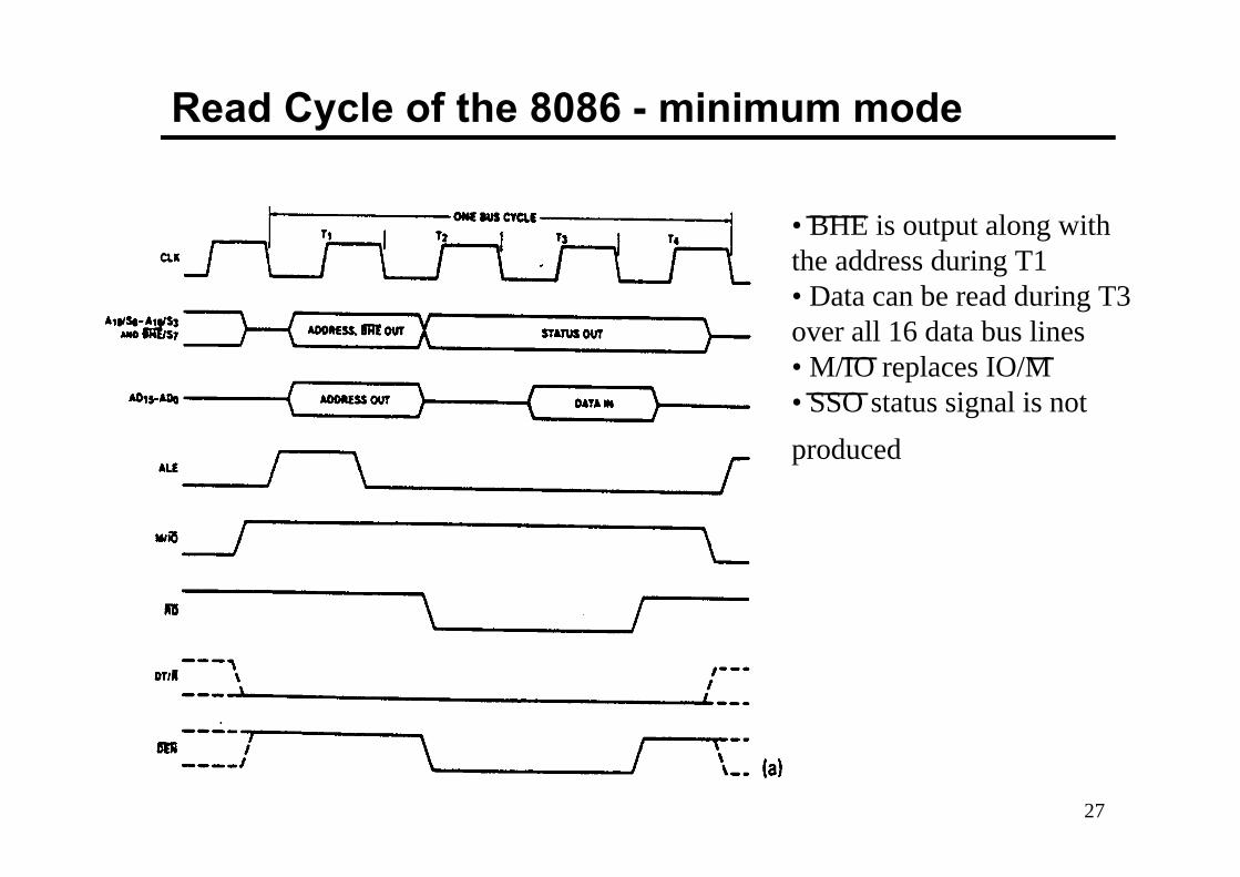
Read Cycle of the 8086 - minimum mode
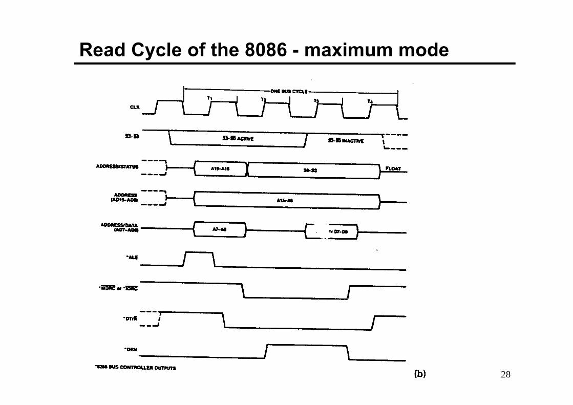
• BHE is output along with the address during T1• Data can be read during T3 over all 16 data bus lines• M/IO replaces IO/M• SSO status signal is not
produced
28
Read Cycle of the 8086 - maximum mode
29
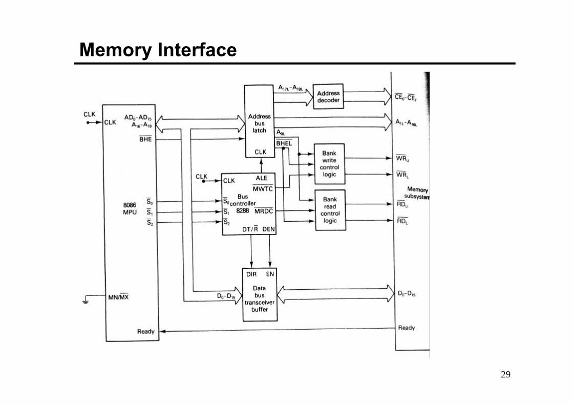
Memory Interface
30
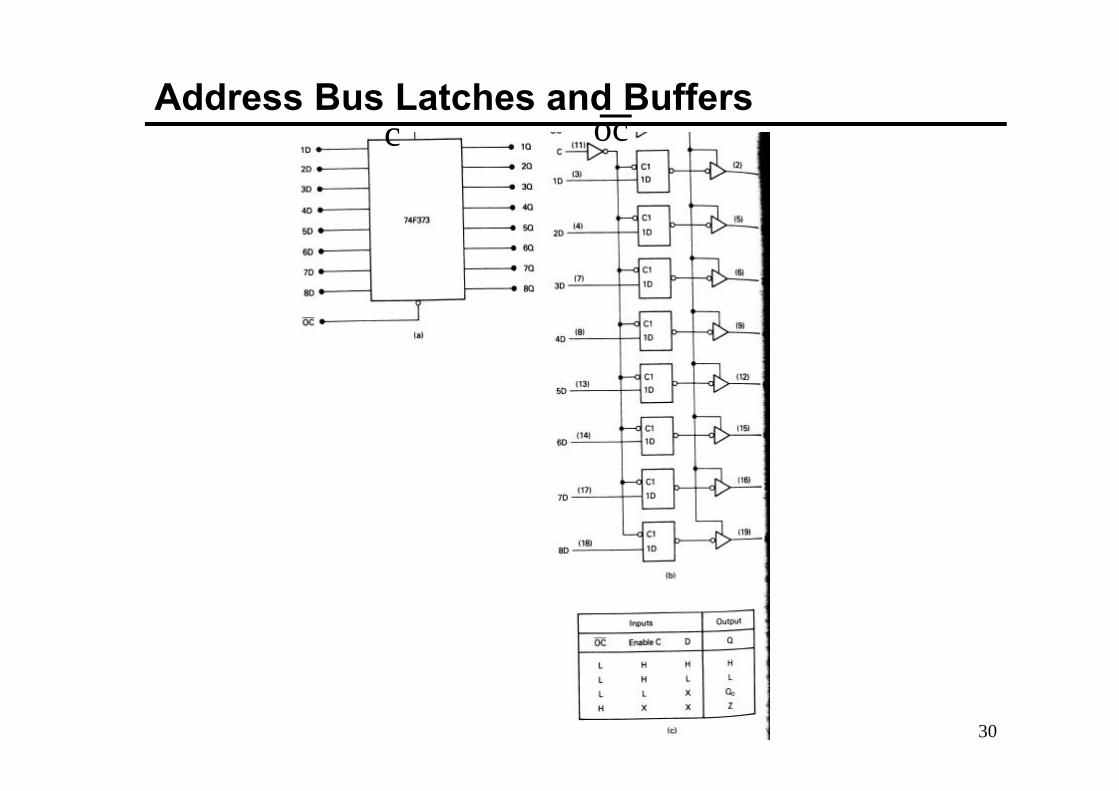
Address Bus Latches and Buffersc oc
31
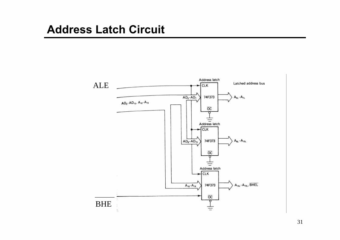
Address Latch Circuit
ALE
BHE
32
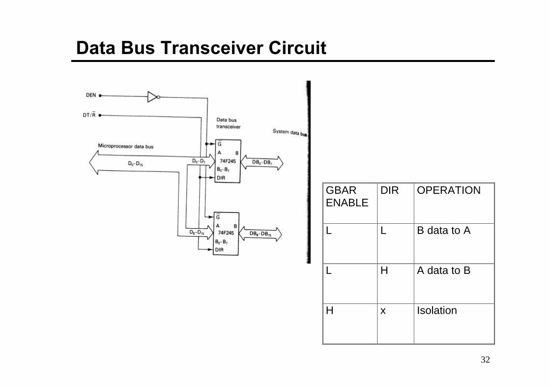
Data Bus Transceiver Circuit
GBARENABLE
DIR OPERATION
L L B data to A
L H A data to B
H x Isolation
33
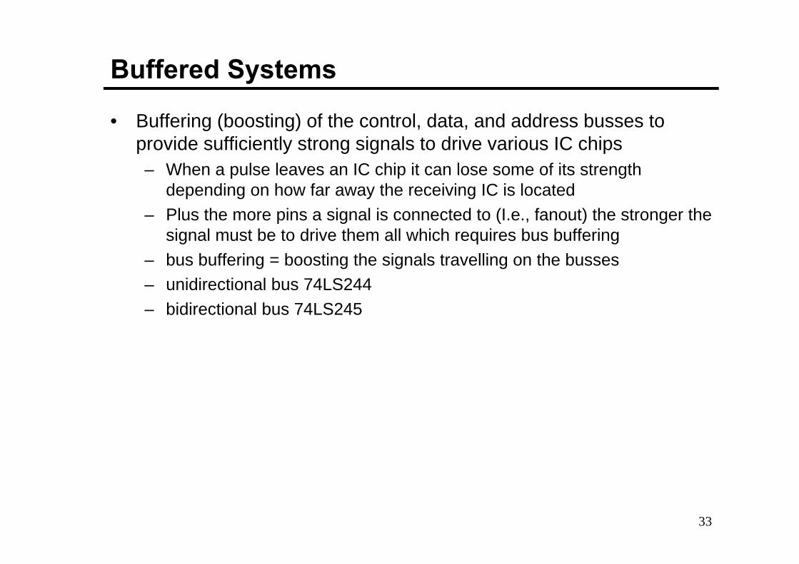
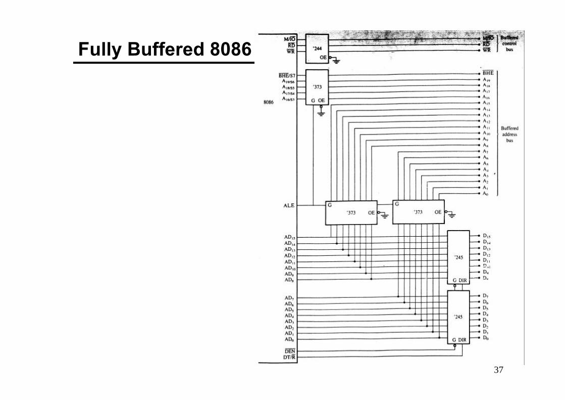
Buffered Systems
• Buffering (boosting) of the control, data, and address busses toprovide sufficiently strong signals to drive various IC chips– When a pulse leaves an IC chip it can lose some of its strength
depending on how far away the receiving IC is located
– Plus the more pins a signal is connected to (I.e., fanout) the stronger the signal must be to drive them all which requires bus buffering
– bus buffering = boosting the signals travelling on the busses
– unidirectional bus 74LS244
– bidirectional bus 74LS245
34
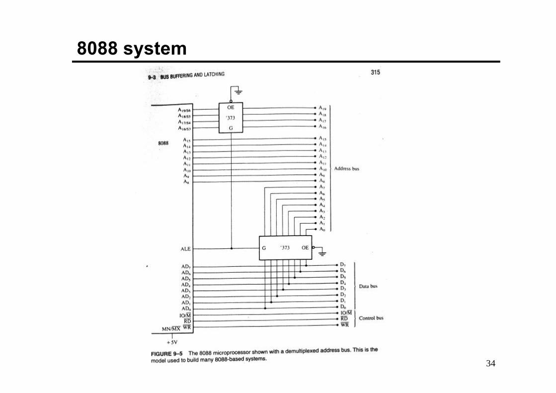
8088 system

35
8086 System
36
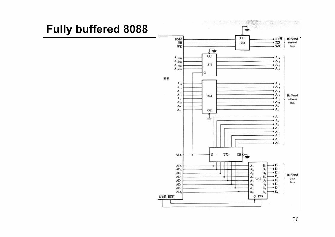
Fully buffered 8088
37
Fully Buffered 8086

38
Bank Write Control Logic
39
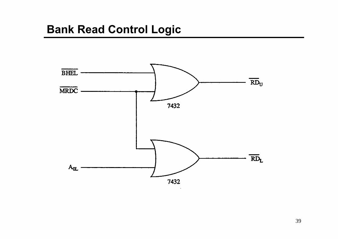
Bank Read Control Logic
40
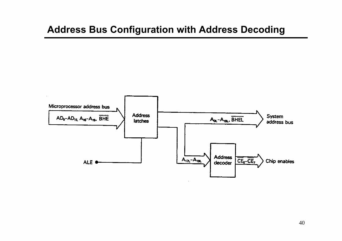
Address Bus Configuration with Address Decoding
41
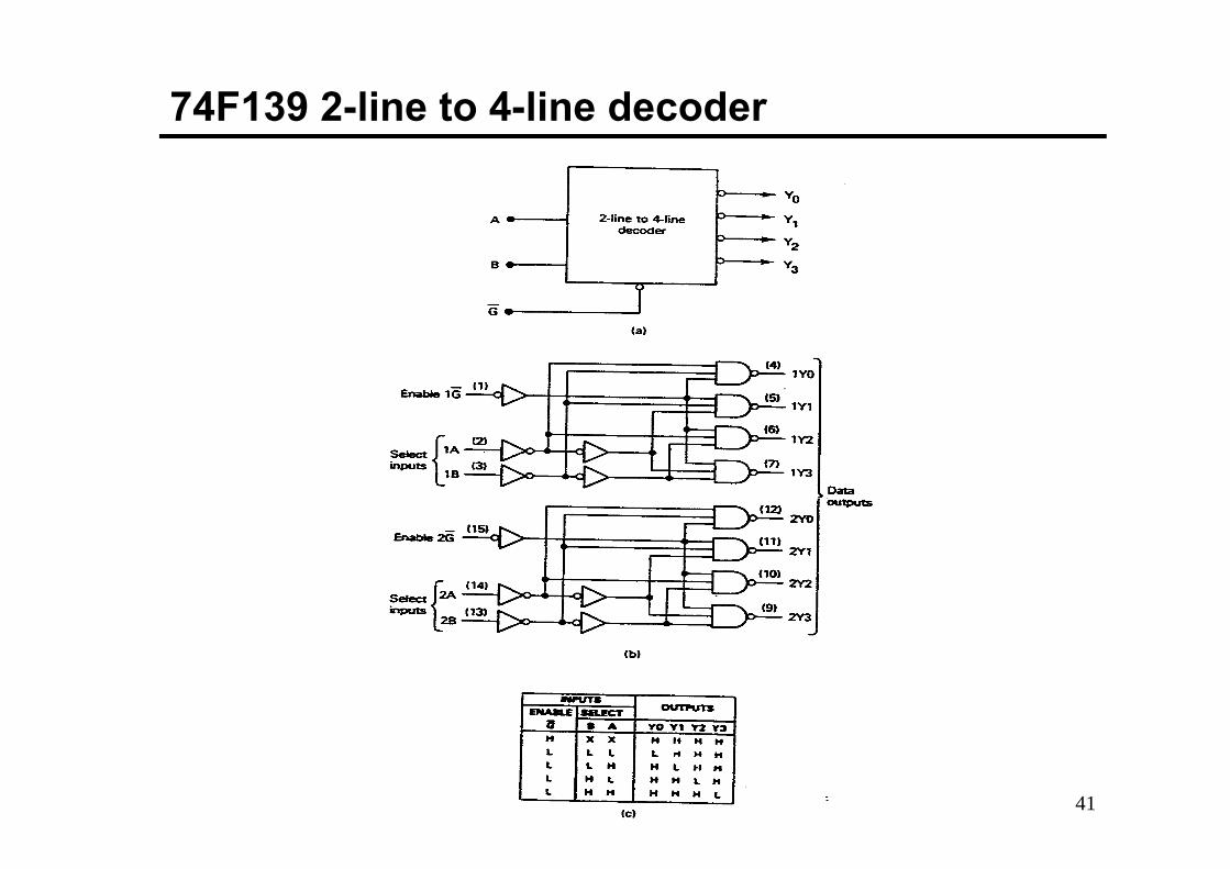
74F139 2-line to 4-line decoder
42
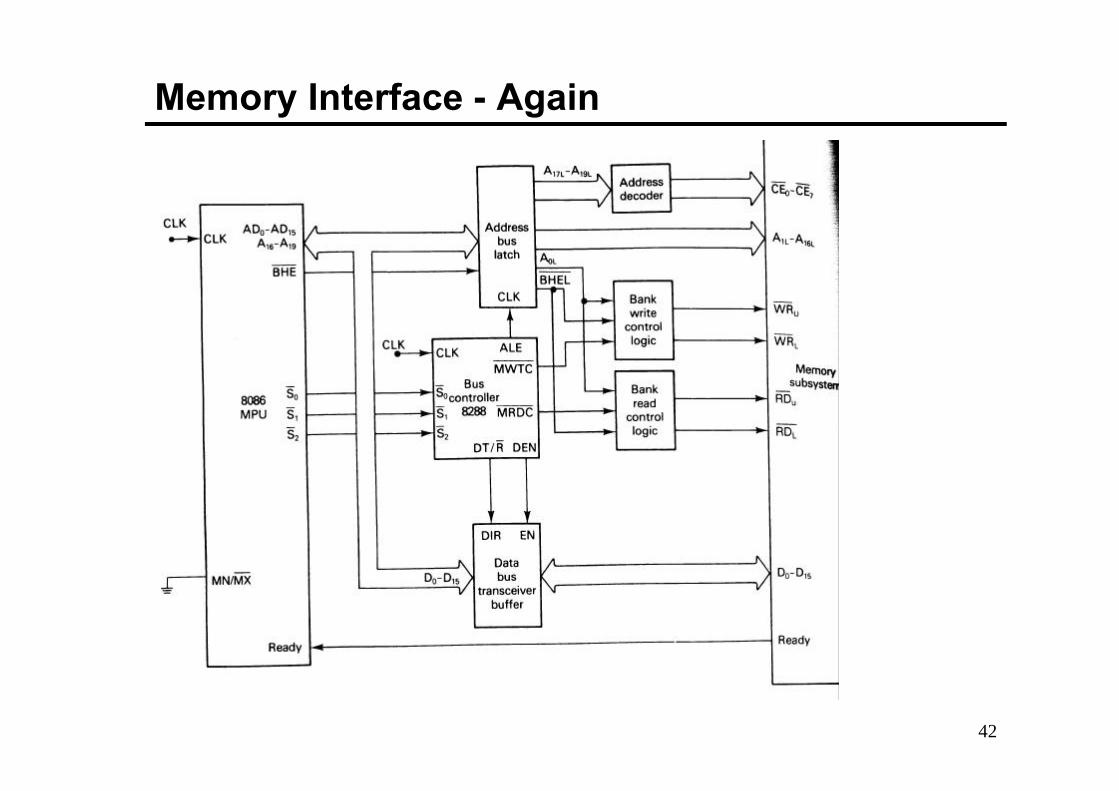
Memory Interface - Again
43
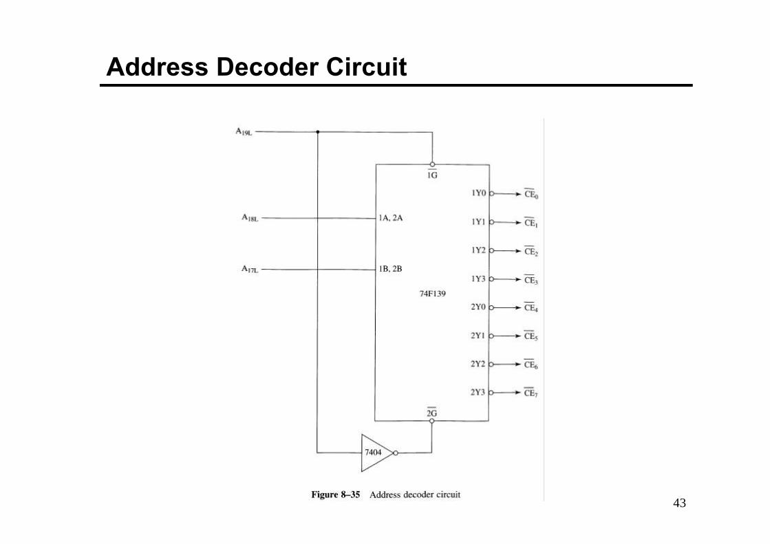
Address Decoder Circuit
44
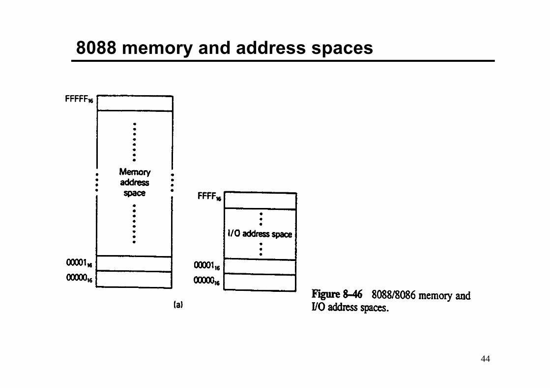
8088 memory and address spaces
45
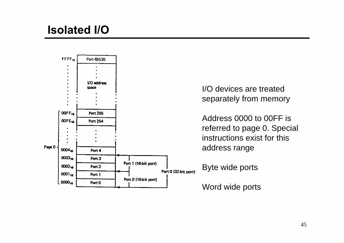
Isolated I/O
I/O devices are treatedseparately from memory
Address 0000 to 00FF is referred to page 0. Special instructions exist for thisaddress range
Byte wide ports
Word wide ports

46
Memory Mapped I/O
47
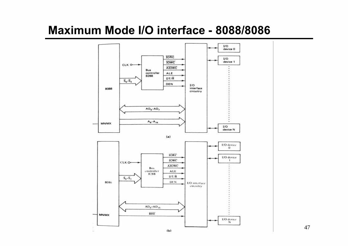
Maximum Mode I/O interface - 8088/8086
48
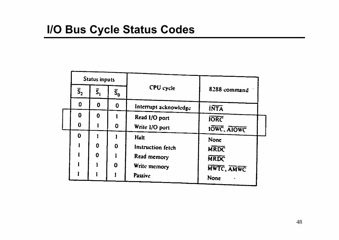
I/O Bus Cycle Status Codes

49
I/O Instructions
Example. Write a sequence of instructions that will output the data FFh to a byte wideoutput at address ABh of the I/O address space
MOV AL,0FFhOUT 0ABh, AL
Example. Data is to be read from two byte wide input ports at addresses AAh and A9hand then this data will then be output to a word wide output port at address B000h
IN AL, 0AAhMOV AH,ALIN AL, 0A9hMOV DX,0B00hOUT DX,AX
50
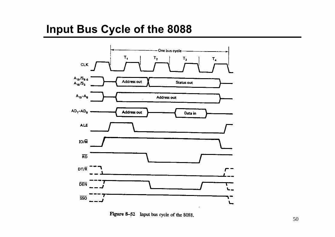
Input Bus Cycle of the 8088
51
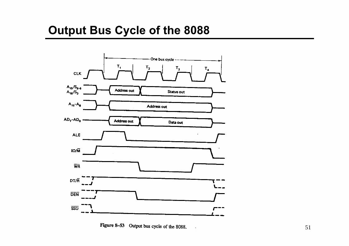
Output Bus Cycle of the 8088