week 1 introduction to computing and the 8051...
TRANSCRIPT

1
Week 1Introduction to Computing and
the 8051 MicrocontrollersChapters 0 and 1

2
Binary and Hexadecimal Systems Conversion to decimal:
❍ 110.101 b = ?❍ 6A.C h = ?
Conversion from decimal❍ for a whole number: divide by the
radix and save the remainder as the significant digits
❍ 10 = ? B❍ 10 = ? 8
Converting from a decimal fraction
❍ multiply the decimal fraction by the radix
❍ save the whole number part of the result
❍ repeat above until fractional part of step 2 is 0
❍ 0.125 = ? b❍ 0.046875 = ? h
❍ 110.101 b = 6.625❍ 6A.C h = 106.75
❍ 10 = 1010 b
❍ 10 = 12 8
❍ 0.125 = 0.001 b❍ 0.046875 = 0.0C h
3
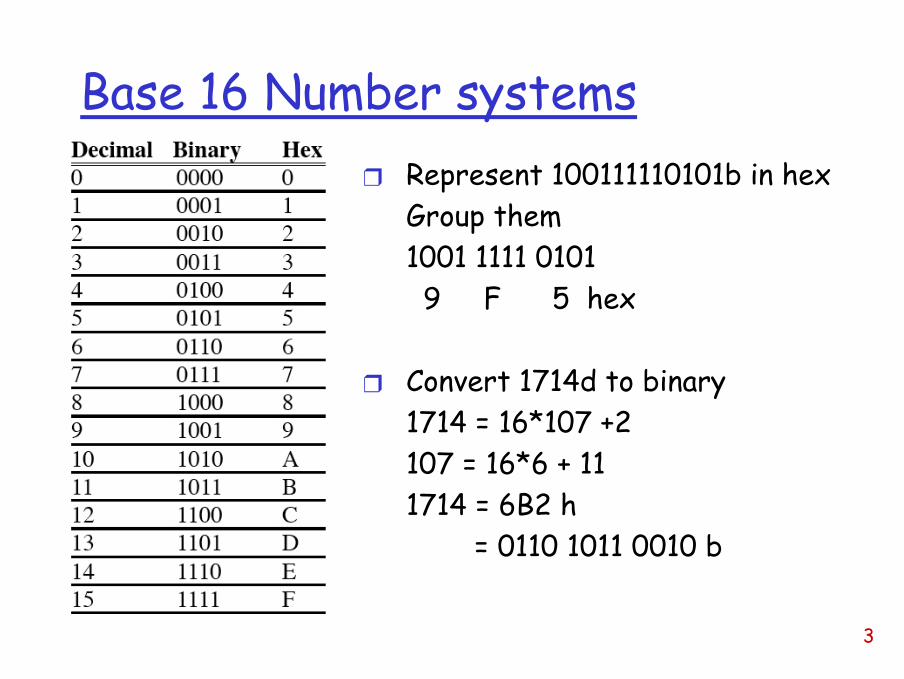
Base 16 Number systems❒ Represent 100111110101b in hex
Group them1001 1111 01019 F 5 hex
❒ Convert 1714d to binary1714 = 16*107 +2107 = 16*6 + 111714 = 6B2 h
= 0110 1011 0010 b
4
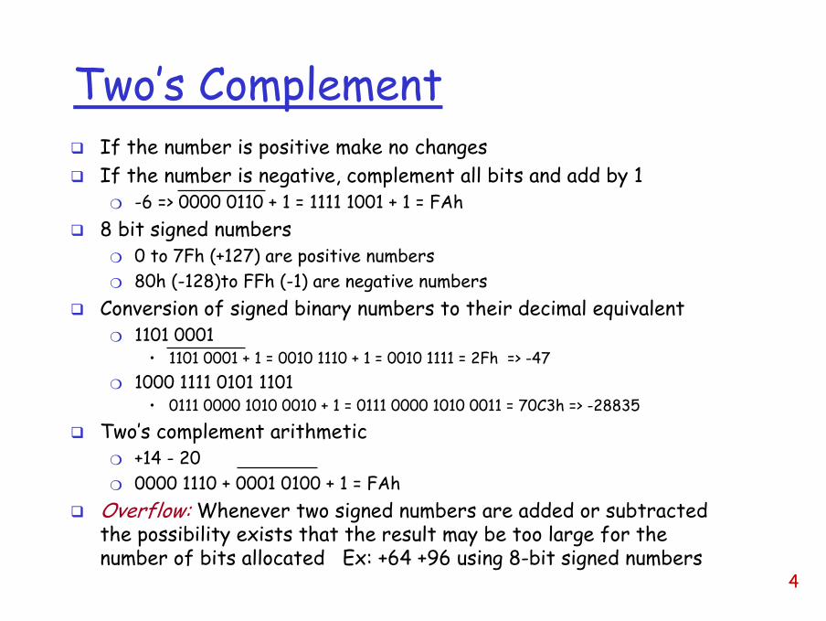
Two’s ComplementIf the number is positive make no changesIf the number is negative, complement all bits and add by 1
❍ -6 => 0000 0110 + 1 = 1111 1001 + 1 = FAh8 bit signed numbers
❍ 0 to 7Fh (+127) are positive numbers❍ 80h (-128)to FFh (-1) are negative numbers
Conversion of signed binary numbers to their decimal equivalent❍ 1101 0001
• 1101 0001 + 1 = 0010 1110 + 1 = 0010 1111 = 2Fh => -47❍ 1000 1111 0101 1101
• 0111 0000 1010 0010 + 1 = 0111 0000 1010 0011 = 70C3h => -28835
Two’s complement arithmetic❍ +14 - 20❍ 0000 1110 + 0001 0100 + 1 = FAh
Overflow: Whenever two signed numbers are added or subtracted the possibility exists that the result may be too large for the number of bits allocated Ex: +64 +96 using 8-bit signed numbers

5
Two’s complement
Numbers in the range -2^n … 2^n –1are represented by 8 bit signed arithmetic
……7Fh0111 1111b+127
01h0000 0001b100h0000 0000b0FFh1111 1111b-1FEh1111 1110b-2……82h1000 0010b-12681h1000 0001b-12780h1000 0000 b-128HexBinaryDecimal

6
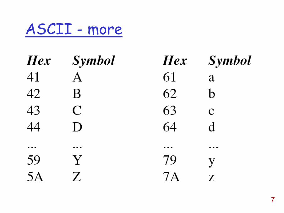
ASCIIThe standard for textIn this code each letter of the alphabet, punctuation mark, and decimal number is assigned a unique 7-bit code numberWith 7 bits, 128 unique symbols can be codedOften a zero is placed in the most significant bit position to make it an 8-bit code❍ e.g., Uppercase A 41h
Digits 0 through 9 are represented by ASCII codes 30h to 39h
7
ASCII - more
8
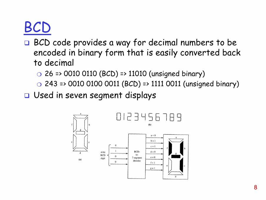
BCDBCD code provides a way for decimal numbers to be encoded in binary form that is easily converted back to decimal
❍ 26 => 0010 0110 (BCD) => 11010 (unsigned binary)❍ 243 => 0010 0100 0011 (BCD) => 1111 0011 (unsigned binary)
Used in seven segment displays

9
Digital Primer
Inversion

10
AND and OR Gates

11
XOR Gate

12
Logic Design using GatesTwo implementations of a half-adder

13
Full adder using half adders

14
3-bit adder using 3 full-adders

15
Multiplexer

16
N to 2N Decoder

17
Address decoders

18
LatchThe simplest memory elementLevel-sensitive: it memorizes the input data when there is a given level on the control input

19
D type flip flop (DFF)The only Flip-Flop we use (forget SR, JK, etc.) The most used memory element Edge-sensitive: it memorizes the input data when there is aspecific transition (e.g., 0 1) on the control input
20
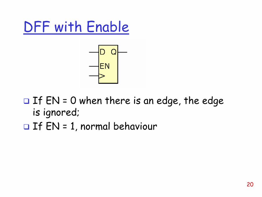
DFF with Enable
If EN = 0 when there is an edge, the edge is ignored; If EN = 1, normal behaviour

21
Registers

22
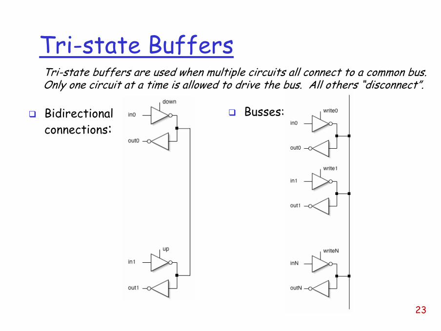
Tri-state BuffersTransistor circuit for inverting tri-state buffer:
“high impedance”(output disconnected)
Variations
Tri-state
“transmission gate”Inverting buffer Inverted enable
23
Tri-state Buffers
Bidirectional connections:
Busses:
Tri-state buffers are used when multiple circuits all connect to a common bus.Only one circuit at a time is allowed to drive the bus. All others “disconnect”.

24
Inside the Computer

25
Inside the Computer - More

26
Stored Program concept

27
Stored Program ConceptThere are three major parts
❍ The CPU (Central Processing Unit) which acts as the brain coordinating all activities within the computer
❍ The memory unit where the program instructions and data are temporarily stored
❍ The I/O (Input/Output) devices which allow the computer to input information for processing and then output the result
Today the CPU circuitry has been reduced to ICscalled the microprocessor, the entire computer with the three parts is called a microcomputer

28
Stored Program Concept - moreSeveral registers (e.g., flip-flops wired in series with each other)
❍ Some are general purpose, the accumulator for example is reserved for performing complex mathematical operations like multiply and divide, and all I/O data has to go thru the accumulator
The basic timing of the computer is controlled by a square wave oscillator or a clock generator circuit.
❍ Synchronization❍ Determines how fast the program can be fetched from
memory and executedMemory Read or Fetch Cycle
❍ IP: Instruction Pointer

29
Stored Program ConceptMemory unit consists of a large number of storage locations each with its own address❍ RAM (Random Access Memory) and its volatility
• Typically each memory location is 8 bits wide (byte accessible memory)
❍ ROM (Read Only Memory)The memory unit’s address selector/decoder circuit examines the binary number on the address line and selects the proper memory location to be accessed.

30
Stored Program Concept
In this example, CPU is reading from memory, it activates its MEMORY READ control signal
❍ This causes the selected data byte in memory to be placed onto the data lines and routed to the instruction register in the CPU
Once in the CPU, the instruction is decoded and executed
❍ In this example, instruction has the decimal code 64 which for a 8086 microprocessor is decoded to be INC AX
❍ The ALU (Arithmetic Logic Unit) is instructed to add 1 to the contents of the AX
The cycle repeats itself

31
Stored Program Concept
Memory unit consists of a large number of storage locations each with its own address.RAM (Random Access Memory): also called read/write memory ❍ used for temporary storage of programs ❍ typically 8 bits wide❍ data is lost when the power is turned off (volatile)ROM (Read Only Memory)❍ The information in ROM is permanent ❍ Non-volatile memory

32
Three Bus System ArchitectureA collection of electronic signals all dedicated to particular task is called a bus
❍ address bus❍ data bus❍ control bus
Data Bus❍ The width of the data bus determines how much data the processor
can read or write in one memory or I/O cycle❍ 8-bit microprocessor has an 8-bit data bus❍ 80386SX 32-bit internal data bus, 16-bit external data bus❍ 80386 32-bit internal and external data buses
How can a 64-bit (or 16 bit) microprocessor access an 8-bit memory?
❍ The trick is to divide the memory into banks❍ 64-bit Pentium requires eight banks of memory with each bank set
up to be one-byte wide❍ Bank enable signals are then output by the microprocessor to
specify which bank to access

33
Address BusAddress Bus
❍ The address bus is used to identify the memory location or I/O device (also called port) the processor intends to communicate with
❍ 20 bits for the 8086 and 8088❍ 32 bits for the 80386/80486
and the Pentium❍ 36 bits for the Pentium II and
III❍ The total number of memory
locations addressable by a given CPU is always equal to 2^x where x is the number of address bits, regardless of the data bus.
Total amount of memory is 4Mbytes
8086 has a 20-bit address bus and therefore addresses all combinations of addresses from all 0s to all 1s. This corresponds to 2 20 addresses or 1M (1 Meg) addresses or memory locations.
Pentium: 4Gbyte main memory

34
Control BusHow can we tell the address is a memory address or an I/O port address
❍ Memory Read❍ Memory Write❍ I/O Read❍ I/O Write
When Memory Read or I/O Read are active, data is input to the processor.When Memory Write or I/O Write are active, data is output from the processor.The control bus signals are defined from the processor’s point of view.Control and address lines are output lines only but the data bus is bidirectional

35
Some Important TerminologyBit is a binary digit that can have the value 0 or 1A byte is defined as 8 bitsA nibble is half a byteA word is two bytesA double word is four bytesA kilobyte is 2^10 bytes (1024 bytes), The abbreviation K is most often used
❍ Example: A floppy disk holding 356Kbytes of dataA megabyte or meg is 2^20 bytes, it is exactly 1,048,576 bytesA gigabyte is 2^30 bytes

36
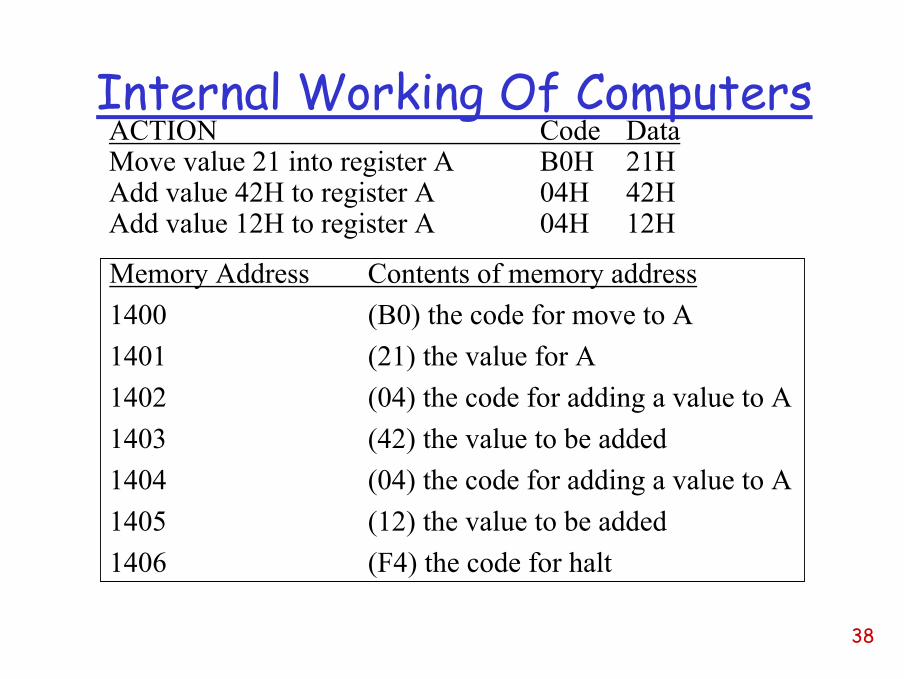
Internal Working of Computers Assume that an imaginary CPU has registers called A,B,C, D.It has an 8-bit data bus and a 16-bit address bus.Therefore the CPU can access memory from addresses 0000h to FFFFh for a total of 2^16 locationsThe action to be performed by the CPU is to put a hexadecimal value 21 into register A, and add to register A values 42h and 12h.Assume that the code for the CPU to move a value to register A is 1011 0000b (B0h) and the code for adding a value to register A is 0000 0100b (04h)
12h04hAdd 12h to A42h04hAdd 42h to A21hB0hMove 21h to ADataCode Action

37
Example Continued
Assume program is stored at memory locations starting at 1400h
F4h (the code for halt)1406h12h1405h04h1404h42h1403h04h1402h21h1401hB0h1400hContent of memoryMemory Address
38
ACTION Code DataMove value 21 into register A B0H 21HAdd value 42H to register A 04H 42HAdd value 12H to register A 04H 12H
Internal Working Of Computers
Memory Address Contents of memory address1400 (B0) the code for move to A1401 (21) the value for A1402 (04) the code for adding a value to A1403 (42) the value to be added1404 (04) the code for adding a value to A1405 (12) the value to be added1406 (F4) the code for halt

39
Internal Working Of Computers1- the CPU program counter can have any value between
0000 FFFF H. This one is set to start with 1400
2- the CPU puts out 1400. The memory circuitry finds the location. Activates the read signal, indicating the memory location 1400. B0 is put on the bus and brought to the CPU
3- B0 is decoded internally it now knows it needs to fetch the next byte!. It brings 21h from 1401. The program counter automatically increments itself to the next location to fetch the next data/instruction.
MEM
CPUPC=1400
Read
B0Inst Decoder
B0 decode
40
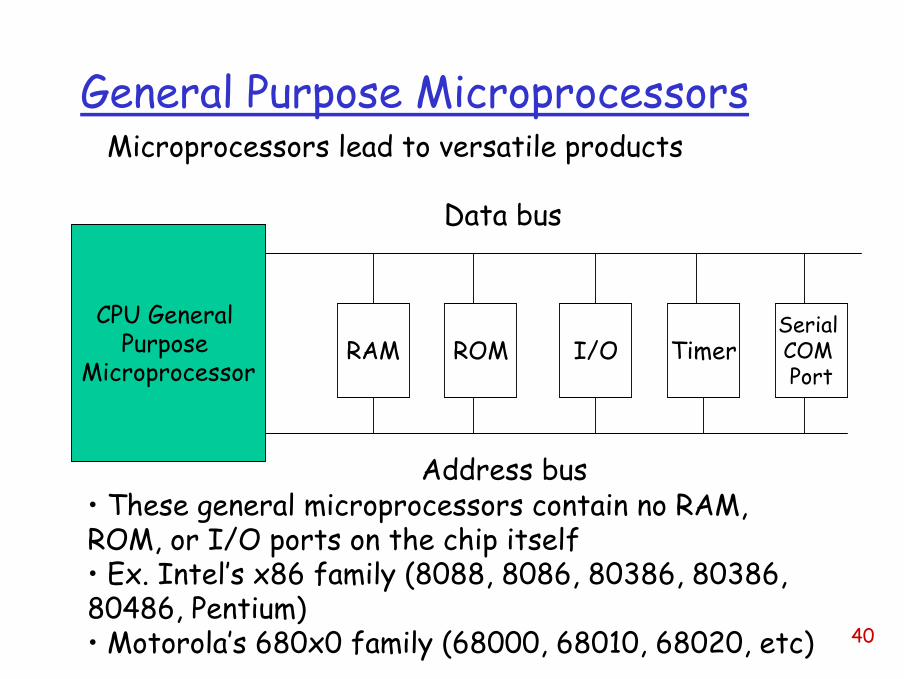
General Purpose Microprocessors
CPU General Purpose
MicroprocessorRAM
Serial COM Port
TimerI/OROM
• These general microprocessors contain no RAM, ROM, or I/O ports on the chip itself• Ex. Intel’s x86 family (8088, 8086, 80386, 80386, 80486, Pentium)• Motorola’s 680x0 family (68000, 68010, 68020, etc)
Data bus
Address bus
Microprocessors lead to versatile products

41
Microcontrollers
CPU RAM ROM
I/O TIMERSerial Com
Port
• A microcontroller has a CPU in addition to a fixed amount of RAM, ROM, I/O ports on one single chip; this makes them ideal for applications in which cost and space are critical• Example: a TV remote control does not need the computing power of a 486
• Examples • Motorola’s 6811,
Intel’s 8051, Zilog’s Z8 and PIC 16X

42
Microprocessor vs microcontroller
MicroprocessorCPU is stand-alone, RAM, ROM, I/O, timer are separateDesigner can decide on the amount of ROM, RAM and I/O ports.General-purposeExpensive
MicrocontrollerCPU, RAM, ROM, I/O and timer are all on a single chipFix amount of on-chip ROM, RAM, I/O portsSingle-purposeInexpensiveFor applications in which cost, power and space are critical

43
Embedded Systems
Embedded system means the processor is embedded into that application.An embedded product uses a microprocessor or microcontroller to do one task only.In an embedded system, there is only one application software that is typically burned into ROM.Table 1-1, some embedded products using microcontrollers. Examples: printer, keyboard, video game player, door opener, copier, ABS, fax machine, camera, cellular phone, keyless entry, microwave...

44
Embedded SystemsAlthough microcontrollers are the preferred choice for embedded systems, there are times that the microcontroller is inadequate for the taskIntel, Motorola, AMD, Cyrix have also targeted the embedded market with their general purpose microprocessorsFor example, Power PC microprocessors (IBM Motorola joint venture) are used in PCs and routers/switches todayMicrocontrollers differ in terms of their RAM,ROM, I/O sizes and type.
❍ ROM: One time-programmable, UV-ROM, flash memory

45
Embedded Systems - more
Which is your choice for an embedded product?microcontroller❍ cost down❍ embedded processor or microcontroller
microprocessor ❍ In future, an entire computer on a chip❍ high-end embedded systems use
microprocessors❍ Advantage: rapid software development, all
(appliances) in one.

46
How to choose a microcontroller
1. meeting the computing needs of the task efficiently and cost effectively
• speed, the amount of ROM and RAM, the number of I/O ports and timers, size, packaging, power consumption
• easy to upgrade• cost per unit
2. availability of software development tools• assemblers, debuggers, C compilers, emulator,
simulator, technical support3. wide availability and reliable sources of the
microcontrollers.
47
Intel 8051
1981, Intel MCS-51The 8051 became popular after Intel allowed other manufacturers to make and market a flavor of the 8051.❍ different speed, amount of on-chip ROM❍ code-compatible with the original 8051❍ form a 8051 family

48
8051 Features
Feature Quantity NotesROM 4K bytes a fixed programRAM 128 bytes temporary dataTimers 2 Timer/counter
0,1I/O pins 32 P0,P1,P2,P3Serial port 1 TxD, RxDInterrupt sources 6

49
Comparison of 8051 Members
Table 1-4 Comparison of the 8051 Family MembersFeature 8051 8052 8031ROM (program space in bytes) 4K 8K 0RAM (bytes) 128 256 128Timers 2 3 2I/O pins 32 32 32Serial port 1 1 1 Interrupt sources 6 8 6
❒ 8031 is referred as ROM-less 8051❒ To use ROM you must add external ROM to it but you lose two ports

50
8051 Layout1234567891011121314151617181920
4039383736353433323130292827262524232221
P1.0P1.1P1.2P1.3P1.4P1.5P1.6P1.7RST
(RXD)P3.0(TXD)P3.1
(T0)P3.4(T1)P3.5
XTAL2XTAL1
GND
(INT0)P3.2(INT1)P3.3
(RD)P3.7(WR)P3.6
VccP0.0(AD0)P0.1(AD1)P0.2(AD2)P0.3(AD3)P0.4(AD4)P0.5(AD5)P0.6(AD6)P0.7(AD7)EA/VPPALE/PROGPSENP2.7(A15)P2.6(A14)P2.5(A13)P2.4(A12)P2.3(A11)P2.2(A10)P2.1(A9)P2.0(A8)
8051(8031)

51
8051 Block Diagram
CPU
On-chip RAM
On-chip ROM for program code
4 I/O Ports
Timer 0
Serial Port
Figure 1-2. Inside the 8051 Microcontroller Block Diagram
OSC
Interrupt Control
External interrupts
Timer 1
Timer/Counter
Bus Control
TxD RxDP0 P1 P2 P3
Address:P0,P2
4K bytes (max: 64K)
128 bytes
4 I/O ports

52Fast
Expensive (SRAM + battery)
UnlimitedByteYesNoNVRAM
Fast to read, slow to erase/write
ModerateLimited (consult datasheet)SectorYesNoFlash
Fast to read, slow to erase/write
ExpensiveLimited (consult datasheet)ByteYesNoEEPROM
FastModerateLimited (consult datasheet)Entire Chip
Yes, with a device programmer
NoEPROM
FastModeraten/an/a
Once, with a device programmer
NoPROM
FastInexpensiven/an/aNoNoMasked ROM
ModerateModerateUnlimitedByteYesYesDRAM
FastExpensiveUnlimitedByteYesYesSRAM
SpeedCost (per Byte)
Max Erase CyclesErase SizeWriteable?Volatile?Type

53
Different 8051 Products
Distinguish by types of ROM:8751 microcontrollerAT89C51 from Atmel CorporationDS89C4x0 from Dallas SemiconductorDS5000 from Dallas SemiconductorOTP (one-time-programmable) version of the 80518051 family from PhilipsNote
❍ Memory is the biggest difference between them; see Chapters 14 and Chapter 15.
4k bytes UV-EPROM, PROM burner, UV-EPROM eraser
flash memory, PROM burner only
flash memory, r/wfrom/to COM port
NV-RAM, r/w from/to PC serial port
for large market

54
DS89C420/430/…
In the lab experiments, we’ll use the MDE8051 trainer which uses the Dallas (now part of Maxim) DS89C420/430.

55
Atmel’s products