wcn3680b/wcn3660b device specification · wcn3680b/wcn3660b ic ensures hardware and software...
TRANSCRIPT

Qualcomm Technologies, Inc.
For additional information or to submit technical questions, go to: https://www.96boards.org/DragonBoard410c/forum Qualcomm Snapdragon is a product of Qualcomm Technologies, Inc. Other Qualcomm products referenced herein are products of Qualcomm Technologies, Inc. or its subsidiaries.
DragonBoard, Qualcomm, and Snapdragon are trademarks of Qualcomm Incorporated, registered in the United States and other countries. Other product and brand names may be trademarks or registered trademarks of their respective owners.
This technical data may be subject to U.S. and international export, re-export, or transfer (“export”) laws. Diversion contrary to U.S.and international law is strictly prohibited.
Use of this document is subject to the license set forth in Exhibit 1.
Qualcomm Technologies, Inc.5775 Morehouse DriveSan Diego, CA 92121
U.S.A.
@ 2017 Qualcomm Technologies, Inc. All rights reserved.
WCN3680B/WCN3660B
Device Specification
LM80-P0436-70 Rev. B
July 18, 2017

LM80-P0436-70 Rev. B MAY CONTAIN U.S. AND INTERNATIONAL EXPORT CONTROLLED INFORMATION 2
Revision history
Revision Date Description
A June 2017 Initial release
B July 2017 Added Figure 3-6 and Figure 3-8

LM80-P0436-70 Rev. B MAY CONTAIN U.S. AND INTERNATIONAL EXPORT CONTROLLED INFORMATION 3
WCN3680B/WCN3660B Device Specification Contents
Contents
1 Introduction . . . . . . . . . . . . . . . . . . . . . . . . . . . . . . . . . . . . . . . . . . . . . . . . . . . . . . . . . . . . . . . 8
1.1 Documentation overview . . . . . . . . . . . . . . . . . . . . . . . . . . . . . . . . . . . . . . . . . . . . . . . . . . 81.2 WCN3680B/WCN3660B device introduction . . . . . . . . . . . . . . . . . . . . . . . . . . . . . . . . . . 91.3 WCN3680B/WCN3660B features . . . . . . . . . . . . . . . . . . . . . . . . . . . . . . . . . . . . . . . . . . 11
1.3.1 WCN3680B/WCN3660B common features . . . . . . . . . . . . . . . . . . . . . . . . . . 111.3.2 Additional features integrated into WCN3680B . . . . . . . . . . . . . . . . . . . . . . . 111.3.3 WLAN features . . . . . . . . . . . . . . . . . . . . . . . . . . . . . . . . . . . . . . . . . . . . . . . . 121.3.4 Bluetooth features . . . . . . . . . . . . . . . . . . . . . . . . . . . . . . . . . . . . . . . . . . . . . . 121.3.5 FM radio features . . . . . . . . . . . . . . . . . . . . . . . . . . . . . . . . . . . . . . . . . . . . . . . 131.3.6 Top-level support features . . . . . . . . . . . . . . . . . . . . . . . . . . . . . . . . . . . . . . . . 131.3.7 Package and other features . . . . . . . . . . . . . . . . . . . . . . . . . . . . . . . . . . . . . . . . 131.3.8 Summary of key WCN3680B/WCN3660B features . . . . . . . . . . . . . . . . . . . . 14
1.4 Terms and acronyms . . . . . . . . . . . . . . . . . . . . . . . . . . . . . . . . . . . . . . . . . . . . . . . . . . . . . 151.5 Special marks . . . . . . . . . . . . . . . . . . . . . . . . . . . . . . . . . . . . . . . . . . . . . . . . . . . . . . . . . . 18
2 Pad definitions . . . . . . . . . . . . . . . . . . . . . . . . . . . . . . . . . . . . . . . . . . . . . . . . . . . . . . . . . . . . 20
2.1 I/O parameter definitions . . . . . . . . . . . . . . . . . . . . . . . . . . . . . . . . . . . . . . . . . . . . . . . . . 232.2 Pad descriptions . . . . . . . . . . . . . . . . . . . . . . . . . . . . . . . . . . . . . . . . . . . . . . . . . . . . . . . . 24
3 Electrical specifications . . . . . . . . . . . . . . . . . . . . . . . . . . . . . . . . . . . . . . . . . . . . . . . . . . 29
3.1 Absolute maximum ratings . . . . . . . . . . . . . . . . . . . . . . . . . . . . . . . . . . . . . . . . . . . . . . . . 293.2 Operating conditions . . . . . . . . . . . . . . . . . . . . . . . . . . . . . . . . . . . . . . . . . . . . . . . . . . . . . 303.3 DC power characteristics . . . . . . . . . . . . . . . . . . . . . . . . . . . . . . . . . . . . . . . . . . . . . . . . . 30
3.3.1 Power mode definitions . . . . . . . . . . . . . . . . . . . . . . . . . . . . . . . . . . . . . . . . . . 303.3.2 Power consumption . . . . . . . . . . . . . . . . . . . . . . . . . . . . . . . . . . . . . . . . . . . . . 31
3.4 Power sequencing . . . . . . . . . . . . . . . . . . . . . . . . . . . . . . . . . . . . . . . . . . . . . . . . . . . . . . . 323.5 WCN3680B/WCN3660B internal LDO regulator . . . . . . . . . . . . . . . . . . . . . . . . . . . . . . 323.6 Digital logic characteristics . . . . . . . . . . . . . . . . . . . . . . . . . . . . . . . . . . . . . . . . . . . . . . . . 323.7 Timing characteristics . . . . . . . . . . . . . . . . . . . . . . . . . . . . . . . . . . . . . . . . . . . . . . . . . . . . 33
3.7.1 Timing diagram conventions . . . . . . . . . . . . . . . . . . . . . . . . . . . . . . . . . . . . . . 333.7.2 Rise and fall time specifications . . . . . . . . . . . . . . . . . . . . . . . . . . . . . . . . . . . 34
3.8 Top-level support . . . . . . . . . . . . . . . . . . . . . . . . . . . . . . . . . . . . . . . . . . . . . . . . . . . . . . . . 343.8.1 I/O block . . . . . . . . . . . . . . . . . . . . . . . . . . . . . . . . . . . . . . . . . . . . . . . . . . . . . . 343.8.2 Master reference clock requirements . . . . . . . . . . . . . . . . . . . . . . . . . . . . . . . . 353.8.3 DC power gating and distribution . . . . . . . . . . . . . . . . . . . . . . . . . . . . . . . . . . 35
3.9 WLAN RF circuits . . . . . . . . . . . . . . . . . . . . . . . . . . . . . . . . . . . . . . . . . . . . . . . . . . . . . . 363.9.1 WLAN 2.4 GHz RF Tx . . . . . . . . . . . . . . . . . . . . . . . . . . . . . . . . . . . . . . . . . . 37
LM80-P0436-70 Rev. B MAY CONTAIN U.S. AND INTERNATIONAL EXPORT CONTROLLED INFORMATION 4
WCN3680B/WCN3660B Device Specification Contents
3.9.2 WLAN 2.4 GHz RF Rx . . . . . . . . . . . . . . . . . . . . . . . . . . . . . . . . . . . . . . . . . . 393.9.3 WLAN 5 GHz RF Tx . . . . . . . . . . . . . . . . . . . . . . . . . . . . . . . . . . . . . . . . . . . . 433.9.4 WLAN 5 GHz RF Rx . . . . . . . . . . . . . . . . . . . . . . . . . . . . . . . . . . . . . . . . . . . . 493.9.5 WLAN analog interface between host and WCN3680B/WCN3660B . . . . . . 493.9.6 WLAN Tx power detector . . . . . . . . . . . . . . . . . . . . . . . . . . . . . . . . . . . . . . . . 51
3.10 Bluetooth radio . . . . . . . . . . . . . . . . . . . . . . . . . . . . . . . . . . . . . . . . . . . . . . . . . . . . . . . . . 523.10.1 Bluetooth RF Tx . . . . . . . . . . . . . . . . . . . . . . . . . . . . . . . . . . . . . . . . . . . . . . . . 523.10.2 Bluetooth RF Rx . . . . . . . . . . . . . . . . . . . . . . . . . . . . . . . . . . . . . . . . . . . . . . . 55
3.11 FM performance specifications . . . . . . . . . . . . . . . . . . . . . . . . . . . . . . . . . . . . . . . . . . . . . 583.11.1 FM analog and RF performance specifications . . . . . . . . . . . . . . . . . . . . . . . . 583.11.2 FM RDS interrupt . . . . . . . . . . . . . . . . . . . . . . . . . . . . . . . . . . . . . . . . . . . . . . 62
4 Mechanical information . . . . . . . . . . . . . . . . . . . . . . . . . . . . . . . . . . . . . . . . . . . . . . . . . . . 63
4.1 Device physical dimensions . . . . . . . . . . . . . . . . . . . . . . . . . . . . . . . . . . . . . . . . . . . . . . . 634.2 Device marking . . . . . . . . . . . . . . . . . . . . . . . . . . . . . . . . . . . . . . . . . . . . . . . . . . . . . . . . . 66
4.2.1 WCN3680B . . . . . . . . . . . . . . . . . . . . . . . . . . . . . . . . . . . . . . . . . . . . . . . . . . . 664.2.2 WCN3660B . . . . . . . . . . . . . . . . . . . . . . . . . . . . . . . . . . . . . . . . . . . . . . . . . . . 67
4.3 Device ordering information . . . . . . . . . . . . . . . . . . . . . . . . . . . . . . . . . . . . . . . . . . . . . . . 684.4 Device moisture-sensitivity level . . . . . . . . . . . . . . . . . . . . . . . . . . . . . . . . . . . . . . . . . . . 684.5 Thermal characteristics . . . . . . . . . . . . . . . . . . . . . . . . . . . . . . . . . . . . . . . . . . . . . . . . . . . 69
5 . . . . . . . . . . . . . . . . . . . . . . . . . .Carrier, storage, and handling information 70
5.1 Shipping . . . . . . . . . . . . . . . . . . . . . . . . . . . . . . . . . . . . . . . . . . . . . . . . . . . . . . . . . . . . . . 705.1.1 Tape and reel information . . . . . . . . . . . . . . . . . . . . . . . . . . . . . . . . . . . . . . . . 705.1.2 Packing for shipment (including bar code label) . . . . . . . . . . . . . . . . . . . . . . . 71
5.2 Storage . . . . . . . . . . . . . . . . . . . . . . . . . . . . . . . . . . . . . . . . . . . . . . . . . . . . . . . . . . . . . . . . 715.2.1 Storage conditions . . . . . . . . . . . . . . . . . . . . . . . . . . . . . . . . . . . . . . . . . . . . . . 715.2.2 Out-of-bag duration . . . . . . . . . . . . . . . . . . . . . . . . . . . . . . . . . . . . . . . . . . . . . 71
5.3 Handling . . . . . . . . . . . . . . . . . . . . . . . . . . . . . . . . . . . . . . . . . . . . . . . . . . . . . . . . . . . . . . 725.3.1 Baking . . . . . . . . . . . . . . . . . . . . . . . . . . . . . . . . . . . . . . . . . . . . . . . . . . . . . . . 725.3.2 Electrostatic discharge . . . . . . . . . . . . . . . . . . . . . . . . . . . . . . . . . . . . . . . . . . . 72
6 PCB mounting guidelines . . . . . . . . . . . . . . . . . . . . . . . . . . . . . . . . . . . . . . . . . . . . . . . . . 73
6.1 Land pad and stencil design . . . . . . . . . . . . . . . . . . . . . . . . . . . . . . . . . . . . . . . . . . . . . . . 736.2 SMT development and characterization . . . . . . . . . . . . . . . . . . . . . . . . . . . . . . . . . . . . . . 736.3 SMT peak package-body temperature . . . . . . . . . . . . . . . . . . . . . . . . . . . . . . . . . . . . . . . 746.4 SMT process verification . . . . . . . . . . . . . . . . . . . . . . . . . . . . . . . . . . . . . . . . . . . . . . . . . 74
7 Part reliability . . . . . . . . . . . . . . . . . . . . . . . . . . . . . . . . . . . . . . . . . . . . . . . . . . . . . . . . . . . . . 75
7.1 Reliability qualification summary . . . . . . . . . . . . . . . . . . . . . . . . . . . . . . . . . . . . . . . . . . . 757.2 Qualification sample description . . . . . . . . . . . . . . . . . . . . . . . . . . . . . . . . . . . . . . . . . . . . 76

LM80-P0436-70 Rev. B MAY CONTAIN U.S. AND INTERNATIONAL EXPORT CONTROLLED INFORMATION 5
WCN3680B/WCN3660B Device Specification
Figures
Figure 2-1 WCN3680B/WCN3660B pad assignments (top view) . . . . . . . . . . . . . . . . . . . . . . . . 20Figure 3-1 Timing diagram conventions . . . . . . . . . . . . . . . . . . . . . . . . . . . . . . . . . . . . . . . . . . . 33Figure 3-3 RF connections for dual-band (2.4 GHz and 5.0 GHz) using SCPC . . . . . . . . . . . . . 36Figure 3-4 RF connections for single-band (2.4 GHz) using SCPC . . . . . . . . . . . . . . . . . . . . . . . 36Figure 3-5 RF switch control for dual-band external 2nd generation FEMs . . . . . . . . . . . . . . . . 45Figure 3-6 RF switch control for dual-band external 3rd generation FEMs . . . . . . . . . . . . . . . . 46Figure 3-7 RF switch control for 2nd generation 5 GHz-only external FEMs . . . . . . . . . . . . . . . 47Figure 3-8 RF switch control for 3rd generation external FEMs . . . . . . . . . . . . . . . . . . . . . . . . . 48Figure 4-1 79B WLNSP outline drawing . . . . . . . . . . . . . . . . . . . . . . . . . . . . . . . . . . . . . . . . . . . 64Figure 4-2 WCN3680B/WCN3660B pad locations . . . . . . . . . . . . . . . . . . . . . . . . . . . . . . . . . . . 65Figure 4-3 WCN3680B part marking (top view – not to scale) . . . . . . . . . . . . . . . . . . . . . . . . . . 66Figure 4-4 WCN3660B part marking (top view – not to scale) . . . . . . . . . . . . . . . . . . . . . . . . . . 67Figure 4-5 Device identification code . . . . . . . . . . . . . . . . . . . . . . . . . . . . . . . . . . . . . . . . . . . . . 68Figure 5-1 Carrier tape drawing with part orientation . . . . . . . . . . . . . . . . . . . . . . . . . . . . . . . . . 70Figure 5-2 Tape handling . . . . . . . . . . . . . . . . . . . . . . . . . . . . . . . . . . . . . . . . . . . . . . . . . . . . . . . 71

LM80-P0436-70 Rev. B MAY CONTAIN U.S. AND INTERNATIONAL EXPORT CONTROLLED INFORMATION 6
WCN3680B/WCN3660B Device Specification
Tables
Table 1-1 Primary WCN3680B/WCN3660B documentation . . . . . . . . . . . . . . . . . . . . . . . . . . . . 8Table 1-2 Reference documents . . . . . . . . . . . . . . . . . . . . . . . . . . . . . . . . . . . . . . . . . . . . . . . . . . . 8Table 1-3 Key WCN3680B/WCN3660B features . . . . . . . . . . . . . . . . . . . . . . . . . . . . . . . . . . . . 14Table 1-4 Terms and acronyms . . . . . . . . . . . . . . . . . . . . . . . . . . . . . . . . . . . . . . . . . . . . . . . . . . . 15Table 1-5 Special marks . . . . . . . . . . . . . . . . . . . . . . . . . . . . . . . . . . . . . . . . . . . . . . . . . . . . . . . . 18Table 2-1 WCN3680B/WCN3660B IC pad assignment in numeric order and location . . . . . . . 21Table 2-2 I/O description (pad type) parameters . . . . . . . . . . . . . . . . . . . . . . . . . . . . . . . . . . . . . 23Table 2-3 Pad descriptions – WLAN functions . . . . . . . . . . . . . . . . . . . . . . . . . . . . . . . . . . . . . . 25Table 2-4 WLAN pad type vs. operating mode . . . . . . . . . . . . . . . . . . . . . . . . . . . . . . . . . . . . . . 25Table 2-5 Pad descriptions – BT functions . . . . . . . . . . . . . . . . . . . . . . . . . . . . . . . . . . . . . . . . . . 26Table 2-6 BT pad type vs. operating mode . . . . . . . . . . . . . . . . . . . . . . . . . . . . . . . . . . . . . . . . . . 26Table 2-7 Pad descriptions – shared WLAN and BT RF front-end functions . . . . . . . . . . . . . . . 26Table 2-8 Pad descriptions – FM radio functions . . . . . . . . . . . . . . . . . . . . . . . . . . . . . . . . . . . . 26Table 2-9 FM pad type vs. operating mode . . . . . . . . . . . . . . . . . . . . . . . . . . . . . . . . . . . . . . . . . 27Table 2-10 Pad descriptions – top-level support functions . . . . . . . . . . . . . . . . . . . . . . . . . . . . . 27Table 2-11 Pad descriptions – no connection, do not connect, and reserved pads . . . . . . . . . . . . 27Table 2-12 Pad descriptions – power supply pads . . . . . . . . . . . . . . . . . . . . . . . . . . . . . . . . . . . . 28Table 2-13 Pad descriptions – ground pads . . . . . . . . . . . . . . . . . . . . . . . . . . . . . . . . . . . . . . . . . 28Table 3-1 Absolute maximum ratings . . . . . . . . . . . . . . . . . . . . . . . . . . . . . . . . . . . . . . . . . . . . . . 29Table 3-2 Operating conditions . . . . . . . . . . . . . . . . . . . . . . . . . . . . . . . . . . . . . . . . . . . . . . . . . . 30Table 3-3 Input power supply current from primary source . . . . . . . . . . . . . . . . . . . . . . . . . . . . . 31Table 3-4 Baseband digital I/O characteristics . . . . . . . . . . . . . . . . . . . . . . . . . . . . . . . . . . . . . . . 32Table 3-5 Capacitive load derating factors . . . . . . . . . . . . . . . . . . . . . . . . . . . . . . . . . . . . . . . . . . 34Table 3-6 Reference requirements . . . . . . . . . . . . . . . . . . . . . . . . . . . . . . . . . . . . . . . . . . . . . . . . 35Table 3-7 WLAN 2.4 GHz RF Tx performance specifications . . . . . . . . . . . . . . . . . . . . . . . . . . 37Table 3-8 WLAN RF Tx emission specifications for WAN concurrency . . . . . . . . . . . . . . . . . . 38Table 3-9 WLAN 2.4 GHz RF Rx performance specifications . . . . . . . . . . . . . . . . . . . . . . . . . . 39Table 3-10 WLAN 2.4 GHz sensitivity degradation with WAN blockers . . . . . . . . . . . . . . . . . . 40Table 3-11 WLAN 5G sensitivity degradation with WAN blockers: part 1 . . . . . . . . . . . . . . . . . 41Table 3-12 WLAN 5G sensitivity degradation with WAN blockers - Part 2 . . . . . . . . . . . . . . . . 42Table 3-13 WLAN 5 GHz RF Tx performance specifications . . . . . . . . . . . . . . . . . . . . . . . . . . 43Table 3-14 5 GHz RF Tx performance – external PA driver . . . . . . . . . . . . . . . . . . . . . . . . . . . . 48Table 3-15 2.4 GHz RF Tx performance – external PA driver . . . . . . . . . . . . . . . . . . . . . . . . . . . 48Table 3-16 5 GHz/20 MHz RF performance – Rx sensitivity . . . . . . . . . . . . . . . . . . . . . . . . . . . 49Table 3-17 Analog interface signals . . . . . . . . . . . . . . . . . . . . . . . . . . . . . . . . . . . . . . . . . . . . . . . 50Table 3-18 Analog I/Q interface specifications . . . . . . . . . . . . . . . . . . . . . . . . . . . . . . . . . . . . . . 50Table 3-19 WLAN Tx power-detector performance specifications . . . . . . . . . . . . . . . . . . . . . . . 51
Table 3-20 Bluetooth Tx performance specifications: basic rate, class1, , . . . . . . . . . . . . . . . . . 52Table 3-21 Bluetooth Tx performance specifications: enhanced data rate . . . . . . . . . . . . . . . . . 53Table 3-22 Bluetooth Tx performance specifications: low-energy mode . . . . . . . . . . . . . . . . . . . 54Table 3-23 Bluetooth Rx performance specifications: basic rate . . . . . . . . . . . . . . . . . . . . . . . . 55

LM80-P0436-70 Rev. B MAY CONTAIN U.S. AND INTERNATIONAL EXPORT CONTROLLED INFORMATION 7
WCN3680B/WCN3660B Device Specification
Table 3-24 Bluetooth Rx performance specifications: enhanced data rate . . . . . . . . . . . . . . . . . 57Table 3-25 Bluetooth Rx performance specifications: low-energy mode . . . . . . . . . . . . . . . . . . 57Table 3-26 FM radio (with RDS) Rx performance specifications . . . . . . . . . . . . . . . . . . . . . . . . 58
Table 3-27 FM receiver selectivity , , , , , . . . . . . . . . . . . . . . . . . . . . . . . . . . . . . . . . . . . . . . . . . . . . . . . . . . . . . .60
Table 4-1 WCN3680B part marking line descriptions . . . . . . . . . . . . . . . . . . . . . . . . . . . . . . . . . 66Table 4-2 WCN3660B part marking line descriptions . . . . . . . . . . . . . . . . . . . . . . . . . . . . . . . . . 67Table 4-3 Device thermal resistance . . . . . . . . . . . . . . . . . . . . . . . . . . . . . . . . . . . . . . . . . . . . . . . 69Table 6-1 SMT reflow profile conditions (for reference only) . . . . . . . . . . . . . . . . . . . . . . . . . . . 74Table 7-1 WCN3680B/WCN3660B reliability qualification report for a device from TSMC and WLNSP package from TSMC and Amkor . . . . . . . . . . . . . . . . . . . . . . . . . . . . . . . . . . . . . . . . . . . . . . . . . 75

LM80-P0436-70 Rev. B MAY CONTAIN U.S. AND INTERNATIONAL EXPORT CONTROLLED INFORMATION 8
1 Introduction
1.1 Documentation overview
This document provides a description of chipset capabilities.
Technical information for the WCN3680B/WCN3660B IC is primarily covered by the documents listed in Table 1-1. Each is a self-contained document, but a thorough understanding of the device and its applications requires familiarization with all of them. Before you begin, you must read the device description in Section 2.1.
Additional reference documents are listed in Table 1-2.
This WCN3680B/WCN3660B device specification is organized as follows:
Chapter 1 Provides an overview of the WCN3680B/WCN3660B documentation, gives a high-level functional description of the device, lists the device features, and defines marking conventions, terms, and acronyms used throughout this document.
Chapter 2 Defines the device pin assignments.
Chapter 3 Defines the device electrical performance specifications, including absolute maximum and operating conditions.
Chapter 4 Provides IC mechanical information, including dimensions, markings, ordering information, moisture sensitivity, and thermal characteristics.
Table 1-1 Primary WCN3680B/WCN3660B documentation
Document no. Title
LM80-P0436-70 WCN3680B/WCN3660B Device Specification
LM80-P0436-71 WCN3660B Device Revision Guide
Table 1-2 Reference documents
Reference Document
1 IEEE 802.11n WLAN MAC and PHY, March 2012
2 IEEE Std 802.11ac-2013
3 Bluetooth Specification Version 4.2, December 2, 2014
4 Bluetooth Radio Frequency TSS and TP Specification 1.2/2.0/2.0 + EDR/2.1/2.1 + EDR/3.0/3.0 + HS/4.0, July 18, 2011
5 Bluetooth Low Energy RF PHY Test Specification, RF-PHY.TS/4.0.0, December 15, 2009
6 ANSI/ESD S20.20-1999, Protection of Electrical and Electronic Parts, Assemblies, and Equipment
LM80-P0436-70 Rev. B MAY CONTAIN U.S. AND INTERNATIONAL EXPORT CONTROLLED INFORMATION 9
WCN3680B/WCN3660B Device Specification Introduction
Chapter 5 Describes shipping, storage, and handling of the WCN3680B/WCN3660B devices.
Chapter 6 Presents procedures and specifications for mounting the WCN3680B/WCN3660B device onto printed circuit boards (PCBs).
Chapter 7 Presents WCN3680B/WCN3660B device reliability data, including a definition of the qualification samples and a summary of qualification test results.
1.2 WCN3680B/WCN3660B device introduction
The WCN3680B/WCN3660B IC integrates four different wireless connectivity technologies into a single device:
Dual-band 2.4 GHz and 5 GHz wireless local area network (WLAN) compliant with the IEEE 802.11a/b/g/n specification and supports optional external PA for both 2.4 GHz and 5 GHz bands
WCN3680B supports 802.11ac (including 256 QAM rates MCS8 and MCS9) for data rates of up to 433 Mbps
Bluetooth compliant with the Bluetooth specification version 4.x (BR/EDR + BLE); ANT+ support
Worldwide FM radio, supporting the Radio Data System (RDS) for Europe and the Radio Broadcast Data System (RBDS) for North America
The WCN3680B/WCN3660B is a highly integrated IC using the 3.805 × 3.82 × 0.63 mm, 79-pin wafer-level nanoscale package (79B WLNSP) and is supplemented by APQ IC processing to create a wireless connectivity solution with minimal part count and PCB area. The WCN3680B/WCN3660B IC ensures hardware and software compatibility with companion Qualcomm Technologies, Inc. (QTI) chipsets.
The WCN3680B/WCN3660B IC uses low-power 65 nm RF CMOS fabrication technology, making it suited for battery-operated devices where power consumption and performance are critical.
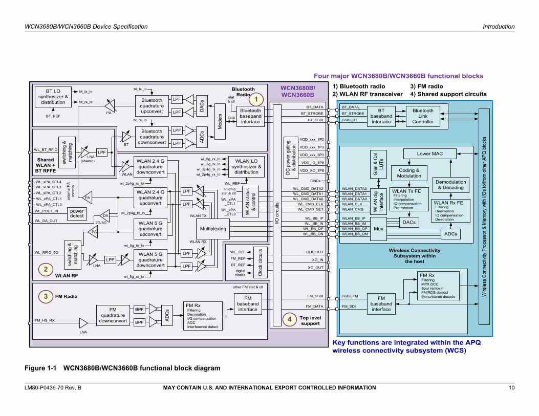
As shown in Figure 1-1, the WCN3680B/WCN3660B device’s major functional blocks are:
Dual-band WLAN RF
Bluetooth radio (RF and digital processing)
FM radio (RF and digital processing)
Shared WLAN + Bluetooth RF front-end (RFFE) circuits
Top-level support circuits that interface with the host IC, buffer the TCXO input, generate the wireless connectivity network (WCN) internal clocks, and gate and distribute DC power to the other blocks.
WCN3680B/WCN3660B Device Specification Introduction
LM80-P0436-70 Rev. B MAY CONTAIN U.S. AND INTERNATIONAL EXPORT CONTROLLED INFORMATION 10
Figure 1-1 WCN3680B/WCN3660B functional block diagram
WL_PDET_IN
WLAN LOsynthesizer &
distribution
WL_xPA_CTL0
powerdetect
LPF
LPF
WLAN 2.4 Gquadrature
downconvert
LPF
LPFWLAN 2.4 Gquadratureupconvert
WL_BT_RFIO
wl_2p4g_tx_lo
WL_xPA_CTL1
WL_BB_IP
PA
LNA(shared)
WL_REF
Multiplexing
Clo
ckci
rcui
ts
FM_DATA
FM_SSBI
Mod
em
Bluetoothbasebandinterface
data
BT_DATA
BT_STROBE
BT_SSBI
WLAN RF
SharedWLAN +BT RFFE
WLAN 5 Gquadratureupconvert
wl_5g_tx_lo
WL_BB_INWL_BB_QPWL_BB_QN
WLAN TX
WLAN RX
WL_CMD_DATA1
WLA
Nst
atus
&co
ntro
l
WL_CMD_DATA0WL_CMD_CLKWL_CMD_SET
WL_CMD_DATA2on-chipstat & ctl
switc
hing
&m
atch
ing
wl_2p4g_rx_lo
WLAN 5 Gquadrature
downconvert
wl_5g_rx_lo
WLAN
BT
Bluetoothquadrature
downconvert
bt_rx_lo
BT_REF
FM_REF
digitalclocks
switc
hing
&m
atch
ing
LNA
PA
WL_RFIO_5G
Bluetoothquadratureupconvert
bt_tx_lo
PA
LPF
LPF ADC
sD
ACs
LPF
LPF
BT LOsynthesizer &
distribution
BT_REF
bt_tx_lo
bt_rx_lostat& ctl
WL_xPA_CTL1
WL_xPA_CTL0
exte
rnal
PAco
ntro
ls
wl_5g_rx_lowl_5g_tx_lo
wl_2p4g_tx_lowl_2p4g_rx_lo D
Cpo
wer
gatin
g&
dist
ribut
ion
VDD_xxx_1P2
Top levelsupport
BluetoothRadio
WCN3680B/WCN3660B
WL_DA_OUT
VDD_xxx_1P3
VDD_xxx_3P3
VDD_IO_1P8
VDD_XO_1P8
GNDsWL_REF
XO_IN
I/Oci
rcui
ts
CLK_OUT
XO_OUT
Wire
less
Con
nect
ivity
Proc
esso
r&M
emor
yw
ithI/O
sto
/from
othe
rAPQ
bloc
ks
BluetoothLink
Controller
BTbasebandinterface
FMbasebandinterface
FM Rx
MuxADCs
WLA
Ndi
gin
terfa
ceG
ain
&C
alLU
Ts
WLAN Tx FE
WLAN Rx FE
Demodulation& Decoding
Coding &Modulation
Lower MAC
BT_DATA
BT_STROBE
SSBI_BT
FM_SDI
SSBI_FM
FilteringMPX DCCSpur removalFM/RDS demodMono/stereo decode
WLAN_BB_IPWLAN_BB_IMWLAN_BB_QPWLAN_BB_QM
DACs
WLAN_DATA1WLAN_DATA0WLAN_CLKWLAN_CMD
WLAN_DATA2
FilteringInterpolationIQ compensationPre-rotation Filtering
DecimationIQ compensationDe-rotation
FM Radio
FM_HS_RX
WL_xPA_CTL4
LNA
BPF
BPF
other FM stat & ctl
ADC
sFMquadrature
downconvert
FMbasebandinterface
FM RxFilteringDecimationI/Q compensationAGCInterference detect
Wireless ConnectivitySubsystem within
the host
LPF
LPF
1) Bluetooth radio2) WLAN RF transceiver
Four major WCN3680B/WCN3660B functional blocks3) FM radio4) Shared support circuits
Key functions are integrated within the APQwireless connectivity subsystem (WCS)
1
2
3
4
WL_xPA_CTL3
WL_xPA_CTL2
DA
2G/5G
LM80-P0436-70 Rev. B MAY CONTAIN U.S. AND INTERNATIONAL EXPORT CONTROLLED INFORMATION 11
WCN3680B/WCN3660B Device Specification Introduction
The WCN3680B/WCN3660B IC includes diverse functions. Its operation can be understood by considering each major functional block individually. This WCN3680B/WCN3660B document set is organized according to the block partitioning listed before Figure 1-1. Information contained in this device specification is organized accordingly, including the circuit groupings within its functional block diagram (Figure 1-1), pin descriptions (Chapter 2), and detailed electrical specifications (Chapter 3).
1.3 WCN3680B/WCN3660B features
NOTE Some of the hardware features integrated within the WCN3660B/WCB3680B must be enabled by software. Refer to the latest version of the applicable software release notes to identify the enabled features.
1.3.1 WCN3680B/WCN3660B common features
Integration of WLAN, Bluetooth, and FM radio functionality
Optional support for 2.4 GHz and 5 GHz external PAs/LNAs for additional performance
Highly integrated front-end eliminates external PA and LNA matching, and antenna Tx/Rx switching
Support for the IEEE 802.11a/b/g/n radio standard
Clock – 48 MHz crystal or 19.2 MHz
65 nm RF CMOS technology in the small 79 WLNSP package
Dual-band WLAN: 2.4 GHz and 5 GHz RF transceivers
Compliant with Bluetooth specification version 4.x
Concurrent WLAN + Bluetooth reception in the 2.4 GHz band
Small IC footprint, low parts count, and minimal PCB area
1.3.2 Additional features integrated into WCN3680B
Added support for 802.11ac
Support 256 QAM modulation schemes (MCS8 and MCS9) for data rates of up to 433 Mbps
Master clock – 48 MHz support only. For exception for single band WCN3660B stuff option designs utilizing PMIC system 19.2 MHz clock, see Section 1.3.6.

LM80-P0436-70 Rev. B MAY CONTAIN U.S. AND INTERNATIONAL EXPORT CONTROLLED INFORMATION 12
WCN3680B/WCN3660B Device Specification Introduction
1.3.3 WLAN features
Advanced power management minimizes power consumption in nonactive modes.
Supports both 2.4 GHz and 5 GHz RF transceivers and compliant with IEEE 802.11a/b/g/n and IEEE 802.11ac (WCN3680B only).
Support for an external PA and an external LNA for applications requiring enhanced 2.4 GHz and 5 GHz performance.
Integrated PA and LNA provides high dynamic Tx output power and excellent Rx sensitivity for extended range.
Internal PAs and T/R switches for both 2.4 GHz and 5 GHz, with the option for an external PA and T/R switch for 2.4 GHz and 5 GHz.
Concurrent WLAN + Bluetooth reception in the 2.4 GHz band.
LTE/ISM coexistence support.
No manufacturing calibration needed.
Host interfaces:
4-line analog baseband interface with Rx/Tx multiplexing
5-line digital command-and-control interface
Other solution-level features
WCN3660B: Support for HT20 and HT40
WCN3680B: Support for HT20, HT40, VHT20, VHT40, and VHT80
Support for 802.11n (WCN3660B and WCN3680B) and 802.11ac (WCN3680B only)
Space-time block coding (STBC) support
Support for short guard interval
Support for other optional 802.11ac features (WCN3680B only), that is, LDPC. MU-MIMO, Tx beamformee
1.3.4 Bluetooth features
Bluetooth 4.x + BR/EDR + BLE
Support for ANT protocol
Support for Bluetooth-WLAN coexistence operation, including optional concurrent receive
Up to 3.5 piconets (master, slave, and page scanning)
Support for class 1 and class 2 power-level transmissions without requiring an external PA
No factory calibration required
APQ interfaces:
Two-line digital data interface supports Rx and Tx
Single-wire serial bus interface (SSBI) for status and control
LM80-P0436-70 Rev. B MAY CONTAIN U.S. AND INTERNATIONAL EXPORT CONTROLLED INFORMATION 13
WCN3680B/WCN3660B Device Specification Introduction
1.3.5 FM radio features
Worldwide FM band support (76 to 108 MHz) with 50 kHz channel spacing
Integrated FM modem receiver with integrated frequency synthesizer
RDS for Europe/RBDS for North America
Integrated RDS/RBDS encoder and decoder (with enable/disable function)
Automatic gain control
Standby mode
Desense-free FM reception when operating with a phone
Host interfaces:
Single-line digital data interface supports Rx
SSBI for status and control
Supports external wired-headset antenna for Rx-only
1.3.6 Top-level support features
System clock options
19.2 MHz TCXO clock for 2.4 GHz only configuration
48 MHz XO for 2.4G and 5G configuration
Clock buffering, gating, and distribution to all other blocks
All WLAN, Bluetooth, and FM interfaces with the host IC are managed by the support block.
DC power-supply gating and distribution to all other blocks
1.3.7 Package and other features
Small package – 3.805 × 3.82 × 0.63 mm 79B WLNSP, 0.4 mm pitch
Many ground pins for improved electrical grounding, mechanical strength, and thermal continuity
Few external components required
RoHS-compliant
LM80-P0436-70 Rev. B MAY CONTAIN U.S. AND INTERNATIONAL EXPORT CONTROLLED INFORMATION 14
WCN3680B/WCN3660B Device Specification Introduction
1.3.8 Summary of key WCN3680B/WCN3660B features
Table 1-3 Key WCN3680B/WCN3660B features
Feature WCN3680B/WCN3660B capability
System
Highly integrated Combination IC with WLAN, Bluetooth, and FM radio functionality
Low parts count and minimal PCB area
Eliminates external PA and LNA matching, and Tx/Rx RF switching
WLAN + Bluetooth Concurrent reception in the 2.4 GHz band
PTA modes for coexistence
Automated calibration No factory calibration required
WLAN RF (digital processing in companion host IC)
Dual-band support 2.4 GHz and 5 GHz RF transceivers
Supports 2.4 GHz and 5 GHz external PA
LTE/ISM coexistence support
WCN3660B: Supports HT20 and HT40 rates
WCN3680B: Supports HT20/VHT20, HT40VHT40, and VHT80 rates
Simple host interfaces 4-line analog baseband interface with Rx/Tx multiplexing
5-line digital command-and-control interface
IEEE 802.11a/b/g/n compliant With companion IC
Other solution-level features WoWLAN support
Support for MCS 0 through 7; up to 150 Mbps data rates
Support for MCS 0 through 9; up to 433 Mbps data rates on WCN3680B
STBC support
Support for short guard interval
Infrastructure, ad-hoc, AP, and Wi-Fi direct operating modes
Bluetooth radio
Bluetooth specification compliance 4.x compliant; 1.x, 2.x + EDR, and 3.0 backward compatible
Highly integrated Baseband modem and 2.4 GHz transceiver; improved Rx sensitivity
Simple host interfaces 2-line digital data interface supports Rx and Tx
SSBI for status and control
Supported modulation GFSK, /4-DQPSK, and 8DPSK (in both directions)
Connectivity Up to seven total wireless connections
Up to 3.5 piconets (master, slave, and page scanning)
One SCO or eSCO connection
Digital processing Modem
Support for all BR, EDR, and BLE packet types
RF Tx power levels Class 1 and 2 transmissions without requiring an external PA
LPPS Reduced device power consumption
ANT Enables communication between self-powered devices
LM80-P0436-70 Rev. B MAY CONTAIN U.S. AND INTERNATIONAL EXPORT CONTROLLED INFORMATION 15
WCN3680B/WCN3660B Device Specification Introduction
1.4 Terms and acronyms
Table 1-4 defines terms and acronyms commonly used throughout this document.
FM radio
Worldwide FM band support 76 to 108 MHz, with 50 kHz channel spacing
Highly integrated Baseband processing and RF receiver
Data system support Radio data system for Europe (RDS)
Radio broadcast data system for North America (RBDS)
Simple host interfaces Single-line digital data interface supports Rx and Tx.
SSBI for status and control
Rx support External wired-headset antenna for Rx only
Highly automated Search and seek; gain control; frequency control; noise cancellation; soft mute; high-cut control; mono/stereo blend; adjustment-free stereo decoder; programmable de-emphasis
Top-level support
Clock 48 MHz crystal
19.2 MHz for single-band 2.4G configuration if disabling 5G
Clock buffering, gating, and distribution to all other blocks
Host IC interfaces Manages all WLAN, Bluetooth, and FM interfaces
DC power Gates and distributes power to all other blocks
Fabrication technology
Single die 65 nm RF CMOS
Package
Small, thermally efficient package 79 WLNSP: 3.805 × 3.82 × 0.63 mm; 0.4 mm pitch
Table 1-3 Key WCN3680B/WCN3660B features (cont.)
Feature WCN3680B/WCN3660B capability
Table 1-4 Terms and acronyms
Term Definition
/4 DQPSK /4 rotated differential quadrature phase shift keying
8DPSK 8-state differential phase shift keying
16 QAM 16-state quadrature amplitude modulation
64 QAM 64-state quadrature amplitude modulation
ACL Asynchronous connection-oriented link
ADC Analog-to-digital converter
AGC Automatic gain control
AP Access point
BB Baseband

LM80-P0436-70 Rev. B MAY CONTAIN U.S. AND INTERNATIONAL EXPORT CONTROLLED INFORMATION 16
WCN3680B/WCN3660B Device Specification Introduction
BER Bit error rate
BLE Bluetooth low energy
BMPS Beacon-mode power save
BOM Bill of materials
BPF Bandpass filter
bps Bits per second
BPSK Binary phase shift keying
BR Basic rate
CCK Complimentary code keying
CDM Charged device model
CDMA Code Division Multiple Access
CLPC Closed loop power control
DAC Digital-to-analog converter
DBPSK Differential binary phase shift keying
DEVM Differential error vector magnitude
DNC Do not connect
DQPSK Differential quadrature phase shift keying
DTIM Delivery traffic indication message
EDR Enhanced data rate
EIRP Effective isotropic radiated power
eSCO Extended synchronous connection-oriented
ESD Electrostatic discharge
ESR Effective series resistance
ETSI European Telecommunications Standards Institute
EVM Error vector magnitude
FBPR Forbidden band power ratio
FCC Federal Communication Commission
FDD Frequency division duplexing
FEM Front-end module
FM Frequency modulation
GFSK Gaussian frequency shift keying
HBM Human body model
HCI Host controller interface
Hi-Z High impedance
I/O Input/output
kbps Kilobits per second
Table 1-4 Terms and acronyms (cont.)
Term Definition

LM80-P0436-70 Rev. B MAY CONTAIN U.S. AND INTERNATIONAL EXPORT CONTROLLED INFORMATION 17
WCN3680B/WCN3660B Device Specification Introduction
LSBit or LSByte Defines whether the LSB is the least significant bit or least significant byte. All instances of LSB used in this manual are assumed to be LSByte, unless otherwise specified.
MSBit or MSByte Defines whether the MSB is the most significant bit or most significant byte. All instances of MSB used in this manual are assumed to be MSByte, unless otherwise specified.
LNA Low-noise amplifier
LO Local oscillator
LPF Low-pass filter
LPO Low-power oscillator
LPPS Low-power page scan
MAC Medium access controller
MCS Modulation coding scheme
MPX Multiplex
MRC Master reference clock
NVM Nonvolatile memory
PA Power amplifier
PCB Printed circuit board
PCM Pulse-coded modulation
PDET Power detector
PER Packet error rate
PHY Physical layer
PLL Phase-locked loop
PM Power management
PMIC Power management integrated circuit
PTA Packet traffic arbitration
QAM Quadrature amplitude modulation
QoS Quality of service
QPSK Quadrature phase shift keying
QTI Qualcomm Technologies, Inc.
RBDS Radio broadcast data system for U.S.A.
RDS Radio data system for Europe
RF Radio frequency
RH Relative humidity
RoHS Restriction of hazardous substances
Rx Receive, receiver
SBI Serial bus interface
Table 1-4 Terms and acronyms (cont.)
Term Definition

LM80-P0436-70 Rev. B MAY CONTAIN U.S. AND INTERNATIONAL EXPORT CONTROLLED INFORMATION 18
WCN3680B/WCN3660B Device Specification Introduction
1.5 Special marks
Table 1-5 defines special marks used in this document.
SCO Synchronous connection-oriented
SCPC Self-calibrated power control
SMT Surface-mount technology
SoC System-on-Chip
Sps Symbols per second (or samples per second)
SSBI Single-wire SBI
STBC Space-time block coding
TCXO Temperature-compensated crystal oscillator
TDD Time-division duplexing
TIM Traffic indication map
TKIP Temporal key integrity protocol
T/R Transmit/receive
Tx Transmit, transmitter
uAPSD Unscheduled automatic power-save delivery
VoIP Voice-over-internet protocol
WAN Wide area network
WEP Wired-equivalent privacy
WLAN Wireless local area network
WLNSP Wafer-level nanoscale package
WMM Wi-Fi multimedia
WMM-AC Wi-Fi multimedia access categories
WoWLAN Wake-on-WLAN
WPA Wi-Fi protected access
XO Crystal oscillator
ZIF Zero intermediate frequency
Table 1-4 Terms and acronyms (cont.)
Term Definition
Table 1-5 Special marks
Mark Definition
[ ] Brackets ([ ]) sometimes follow a pin, register, or bit name. These brackets enclose a range of numbers. For example, DATA[7:4] indicates a range that is 4 bits in length, or DATA[7:0] refers to all eight DATA pins.
_N A suffix of _N indicates an active low signal. For example, RESIN_N.
LM80-P0436-70 Rev. B MAY CONTAIN U.S. AND INTERNATIONAL EXPORT CONTROLLED INFORMATION 19
WCN3680B/WCN3660B Device Specification Introduction
0x0000 Hexadecimal numbers are identified with a 0x prefix in the number, for example, 0x0000. All numbers are decimal (base 10) unless otherwise specified. Nonobvious binary numbers have the term binary enclosed in parentheses at the end of the number, for example, 0011 (binary).
| A vertical bar in the outside margin of a page indicates that a change was made since the previous revision of this document.
Table 1-5 Special marks (cont.)
Mark Definition
LM80-P0436-70 Rev. B MAY CONTAIN U.S. AND INTERNATIONAL EXPORT CONTROLLED INFORMATION 20
2 Pad definitions
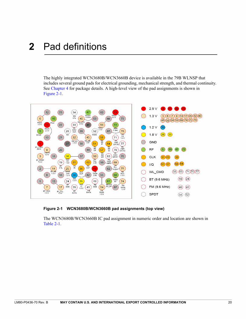
The highly integrated WCN3680B/WCN3660B device is available in the 79B WLNSP that includes several ground pads for electrical grounding, mechanical strength, and thermal continuity. See Chapter 4 for package details. A high-level view of the pad assignments is shown in Figure 2-1.
Figure 2-1 WCN3680B/WCN3660B pad assignments (top view)
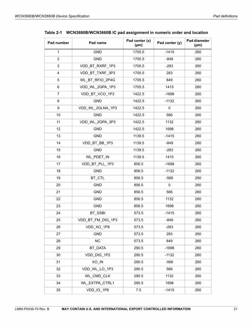
The WCN3680B/WCN3660B IC pad assignment in numeric order and location are shown in Table 2-1.
LM80-P0436-70 Rev. B MAY CONTAIN U.S. AND INTERNATIONAL EXPORT CONTROLLED INFORMATION 21
WCN3680B/WCN3660B Device Specification Pad definitions
Table 2-1 WCN3680B/WCN3660B IC pad assignment in numeric order and location
Pad number Pad namePad center (x)
(µm)Pad center (y)
Pad diameter (µm)
1 GND 1705.5 -1415 260
2 GND 1705.5 -849 260
3 VDD_BT_RXRF_1P3 1705.5 -283 260
4 VDD_BT_TXRF_3P3 1705.5 283 260
5 WL_BT_RFIO_2P4G 1705.5 849 260
6 VDD_WL_2GPA_1P3 1705.5 1415 260
7 VDD_BT_VCO_1P3 1422.5 -1698 260
8 GND 1422.5 -1132 260
9 VDD_WL_2GLNA_1P3 1422.5 0 260
10 GND 1422.5 566 260
11 VDD_WL_2GPA_3P3 1422.5 1132 260
12 GND 1422.5 1698 260
13 GND 1139.5 -1415 260
14 VDD_BT_BB_1P3 1139.5 -849 260
15 GND 1139.5 -283 260
16 WL_PDET_IN 1139.5 1415 260
17 VDD_BT_PLL_1P3 856.5 -1698 260
18 GND 856.5 -1132 260
19 BT_CTL 856.5 -566 260
20 GND 856.5 0 260
21 GND 856.5 566 260
22 GND 856.5 1132 260
23 GND 856.5 1698 260
24 BT_SSBI 573.5 -1415 260
25 VDD_BT_FM_DIG_1P3 573.5 -849 260
26 VDD_XO_1P8 573.5 -283 260
27 GND 573.5 283 260
28 NC 573.5 849 260
29 BT_DATA 290.5 -1698 260
30 VDD_DIG_1P2 290.5 -1132 260
31 XO_IN 290.5 -566 260
32 VDD_WL_LO_1P3 290.5 566 260
33 WL_CMD_CLK 290.5 1132 260
34 WL_EXTPA_CTRL1 290.5 1698 260
35 VDD_IO_1P8 7.5 -1415 260

LM80-P0436-70 Rev. B MAY CONTAIN U.S. AND INTERNATIONAL EXPORT CONTROLLED INFORMATION 22
WCN3680B/WCN3660B Device Specification Pad definitions
36 CLK_OUT 7.5 -849 260
37 GND 7.5 -283 260
38 GND 7.5 283 260
39 GND 7.5 849 260
40 VDD_WL_UPC_1P3 7.5 1415 260
41 FM_DATA -275.5 -1698 260
42 GND -275.5 -1132 260
43 XO_OUT -275.5 -566 260
44 GND -275.5 0 260
45 VDD_WL_BB_1P3 -275.5 566 260
46 GND -275.5 1132 260
47 WL_RF_DA_OUT -275.5 1698 260
48 FM_SSBI -558.5 -1415 260
49 WL_EXTPA_CTRL2 -558.5 -849 260
50 VDD_WL_PLL_1P3 -558.5 -283 260
51 WL_BB_QP -558.5 283 260
52 WL_EXTPA_CTRL0 -558.5 849 260
53 GND -558.5 1415 260
54 VDD_FM_RXBB_1P3 -841.5 -1698 260
55 GND -841.5 -1132 260
56 WL_EXTPA_CTRL4 -841.5 -566 260
57 WL_BB_QN -841.5 0 260
58 WL_BB_IP -841.5 566 260
59 VDD_WL_5GPA_1P3 -841.5 1132 260
60 GND -841.5 1698 260
61 FM_HS_RX -1124.5 -1415 260
62 GND -1124.5 -849 260
63 WL_CMD_SET -1124.5 -283 260
64 WL_BB_IN -1124.5 283 260
65 GND -1124.5 849 260
66 GND -1124.5 1415 260
67 GND -1407.5 -1698 260
68 WL_EXTPA_CTRL3 -1407.5 -1132 260
69 VDD_FM_PLL_1P3 -1407.5 -566 260
70 WL_CMD_DATA1 -1407.5 0 260
Table 2-1 WCN3680B/WCN3660B IC pad assignment in numeric order and location (cont.)
Pad number Pad namePad center (x)
(µm)Pad center (y)
Pad diameter (µm)

LM80-P0436-70 Rev. B MAY CONTAIN U.S. AND INTERNATIONAL EXPORT CONTROLLED INFORMATION 23
WCN3680B/WCN3660B Device Specification Pad definitions
2.1 I/O parameter definitions
71 WL_CMD_DATA0 -1407.5 566 260
72 WL_RFIO_5G/RF_5GHZ_RX -1407.5 1132 260
73 VDD_WL_5GPA_3P3 -1407.5 1698 260
74 VDD_FM_RXFE_1P3 -1690.5 -1415 260
75 VDD_FM_VCO_1P3 -1690.5 -849 260
76 GND -1690.5 -283 260
77 WL_CMD_DATA2 -1690.5 283 260
78 VDD_WL_5GLNA_1P3 -1690.5 849 260
79 GND -1690.5 1415 260
Table 2-1 WCN3680B/WCN3660B IC pad assignment in numeric order and location (cont.)
Pad number Pad namePad center (x)
(µm)Pad center (y)
Pad diameter (µm)
Table 2-2 I/O description (pad type) parameters
Symbol Description
Pad attribute
AI Analog input (does not include pad circuitry)
AO Analog output (does not include pad circuitry)
B Bidirectional digital with CMOS input
DI Digital input (CMOS)
DO Digital output (CMOS)
Z High-impedance (high-Z) output
Pad pull details for digital I/Os
NP Contains no internal pull
PU Contains an internal pull-up device
PD Contains an internal pull-down device
Pad voltages for digital I/Os
DIO Digital interfaces with the host IC VDD_IO_1P8
EPA Control signals to external FEM (VDD_xxx_3P3)
LM80-P0436-70 Rev. B MAY CONTAIN U.S. AND INTERNATIONAL EXPORT CONTROLLED INFORMATION 24
WCN3680B/WCN3660B Device Specification Pad definitions
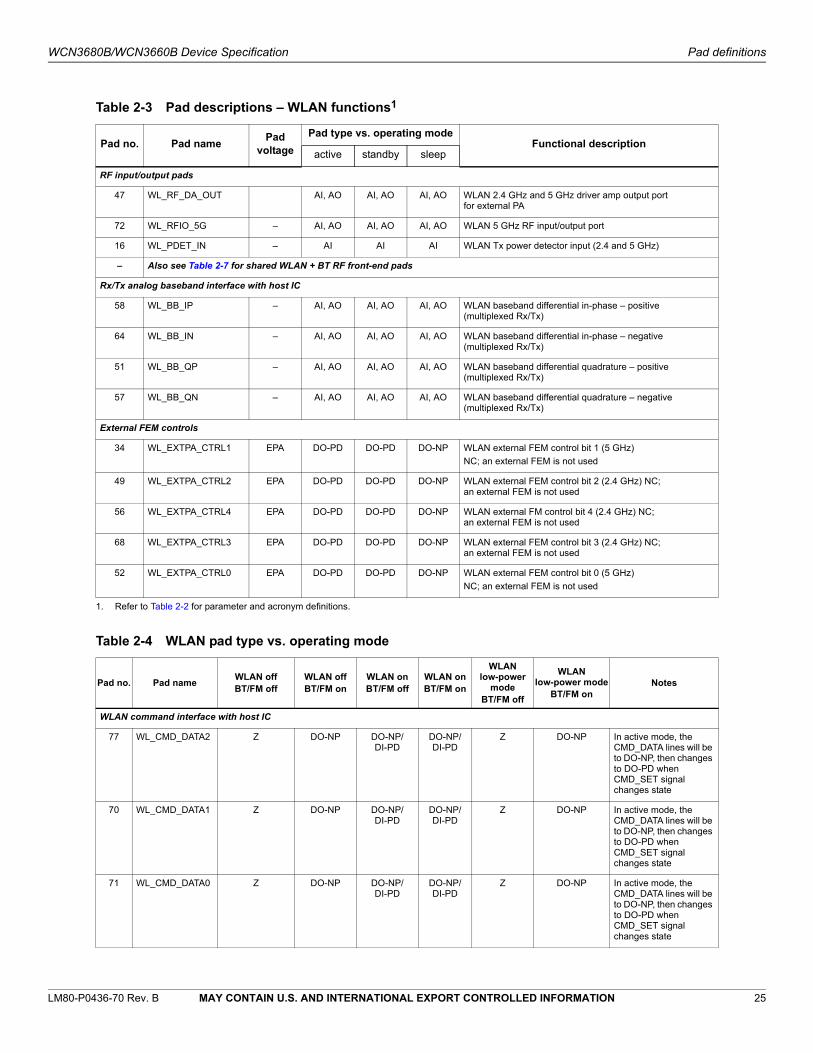
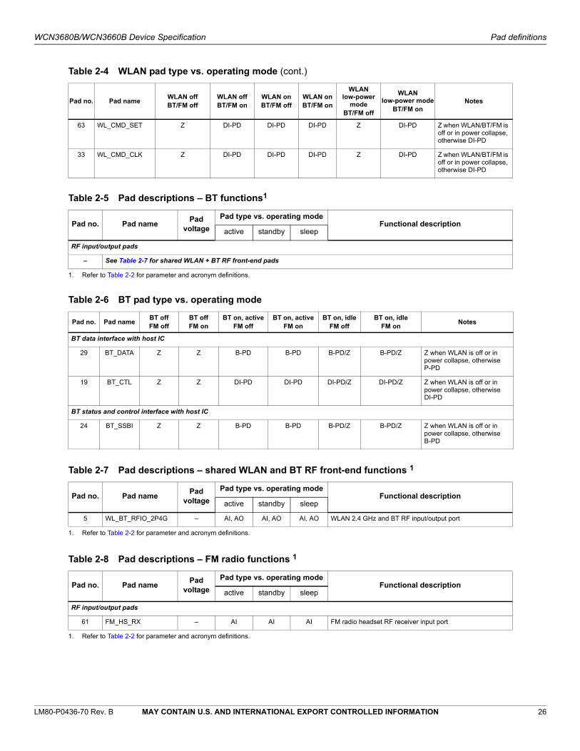
2.2 Pad descriptions
Descriptions of all pads are presented in the following tables, organized by functional group:
Table 2-3 WLAN functions
Table 2-4 WLAN pad type vs. operating mode
Table 2-5 BT functions
Table 2-6 BT pad type vs. operating mode
Table 2-7 Shared WLAN and BT RF front-end functions
Table 2-8 FM radio functions
Table 2-9 FM pad type vs. operating mode
Table 2-10 Top-level support functions
Table 2-11 No connection, do not connect, and reserved pads
Table 2-12 Power supply (PWR) pads
Table 2-13 Ground (GND) pads
LM80-P0436-70 Rev. B MAY CONTAIN U.S. AND INTERNATIONAL EXPORT CONTROLLED INFORMATION 25
WCN3680B/WCN3660B Device Specification Pad definitions
Table 2-3 Pad descriptions – WLAN functions1
1. Refer to Table 2-2 for parameter and acronym definitions.
Pad no. Pad namePad
voltage
Pad type vs. operating modeFunctional description
active standby sleep
RF input/output pads
47 WL_RF_DA_OUT AI, AO AI, AO AI, AO WLAN 2.4 GHz and 5 GHz driver amp output port for external PA
72 WL_RFIO_5G – AI, AO AI, AO AI, AO WLAN 5 GHz RF input/output port
16 WL_PDET_IN – AI AI AI WLAN Tx power detector input (2.4 and 5 GHz)
– Also see Table 2-7 for shared WLAN + BT RF front-end pads
Rx/Tx analog baseband interface with host IC
58 WL_BB_IP – AI, AO AI, AO AI, AO WLAN baseband differential in-phase – positive (multiplexed Rx/Tx)
64 WL_BB_IN – AI, AO AI, AO AI, AO WLAN baseband differential in-phase – negative (multiplexed Rx/Tx)
51 WL_BB_QP – AI, AO AI, AO AI, AO WLAN baseband differential quadrature – positive (multiplexed Rx/Tx)
57 WL_BB_QN – AI, AO AI, AO AI, AO WLAN baseband differential quadrature – negative (multiplexed Rx/Tx)
External FEM controls
34 WL_EXTPA_CTRL1 EPA DO-PD DO-PD DO-NP WLAN external FEM control bit 1 (5 GHz)
NC; an external FEM is not used
49 WL_EXTPA_CTRL2 EPA DO-PD DO-PD DO-NP WLAN external FEM control bit 2 (2.4 GHz) NC; an external FEM is not used
56 WL_EXTPA_CTRL4 EPA DO-PD DO-PD DO-NP WLAN external FM control bit 4 (2.4 GHz) NC; an external FEM is not used
68 WL_EXTPA_CTRL3 EPA DO-PD DO-PD DO-NP WLAN external FEM control bit 3 (2.4 GHz) NC; an external FEM is not used
52 WL_EXTPA_CTRL0 EPA DO-PD DO-PD DO-NP WLAN external FEM control bit 0 (5 GHz)
NC; an external FEM is not used
Table 2-4 WLAN pad type vs. operating mode
Pad no. Pad nameWLAN off BT/FM off
WLAN offBT/FM on
WLAN onBT/FM off
WLAN onBT/FM on
WLAN low-power
modeBT/FM off
WLAN low-power mode
BT/FM onNotes
WLAN command interface with host IC
77 WL_CMD_DATA2 Z DO-NP DO-NP/DI-PD
DO-NP/DI-PD
Z DO-NP In active mode, the CMD_DATA lines will be to DO-NP, then changes to DO-PD when CMD_SET signal changes state
70 WL_CMD_DATA1 Z DO-NP DO-NP/DI-PD
DO-NP/DI-PD
Z DO-NP In active mode, the CMD_DATA lines will be to DO-NP, then changes to DO-PD when CMD_SET signal changes state
71 WL_CMD_DATA0 Z DO-NP DO-NP/DI-PD
DO-NP/DI-PD
Z DO-NP In active mode, the CMD_DATA lines will be to DO-NP, then changes to DO-PD when CMD_SET signal changes state
LM80-P0436-70 Rev. B MAY CONTAIN U.S. AND INTERNATIONAL EXPORT CONTROLLED INFORMATION 26
WCN3680B/WCN3660B Device Specification Pad definitions
63 WL_CMD_SET Z DI-PD DI-PD DI-PD Z DI-PD Z when WLAN/BT/FM is off or in power collapse, otherwise DI-PD
33 WL_CMD_CLK Z DI-PD DI-PD DI-PD Z DI-PD Z when WLAN/BT/FM is off or in power collapse, otherwise DI-PD
Table 2-5 Pad descriptions – BT functions1
1. Refer to Table 2-2 for parameter and acronym definitions.
Pad no. Pad namePad
voltage
Pad type vs. operating modeFunctional description
active standby sleep
RF input/output pads
– See Table 2-7 for shared WLAN + BT RF front-end pads
Table 2-6 BT pad type vs. operating mode
Pad no. Pad nameBT offFM off
BT offFM on
BT on, activeFM off
BT on, activeFM on
BT on, idleFM off
BT on, idleFM on
Notes
BT data interface with host IC
29 BT_DATA Z Z B-PD B-PD B-PD/Z B-PD/Z Z when WLAN is off or in power collapse, otherwise P-PD
19 BT_CTL Z Z DI-PD DI-PD DI-PD/Z DI-PD/Z Z when WLAN is off or in power collapse, otherwise DI-PD
BT status and control interface with host IC
24 BT_SSBI Z Z B-PD B-PD B-PD/Z B-PD/Z Z when WLAN is off or in power collapse, otherwise B-PD
Table 2-7 Pad descriptions – shared WLAN and BT RF front-end functions 1
1. Refer to Table 2-2 for parameter and acronym definitions.
Pad no. Pad namePad
voltage
Pad type vs. operating modeFunctional description
active standby sleep
5 WL_BT_RFIO_2P4G – AI, AO AI, AO AI, AO WLAN 2.4 GHz and BT RF input/output port
Table 2-8 Pad descriptions – FM radio functions 1
1. Refer to Table 2-2 for parameter and acronym definitions.
Pad no. Pad namePad
voltage
Pad type vs. operating modeFunctional description
active standby sleep
RF input/output pads
61 FM_HS_RX – AI AI AI FM radio headset RF receiver input port
Table 2-4 WLAN pad type vs. operating mode (cont.)
Pad no. Pad nameWLAN off BT/FM off
WLAN offBT/FM on
WLAN onBT/FM off
WLAN onBT/FM on
WLAN low-power
modeBT/FM off
WLAN low-power mode
BT/FM onNotes

LM80-P0436-70 Rev. B MAY CONTAIN U.S. AND INTERNATIONAL EXPORT CONTROLLED INFORMATION 27
WCN3680B/WCN3660B Device Specification Pad definitions
Table 2-9 FM pad type vs. operating mode
Pad no. Pad nameBT offFM off
BT offFM on
BT on, activeFM off
BT on, activeFM on
BT on, idleFM off
BT on, idleFM on
FM data interface with host IC
41 FM_DATA Z B-PD Z B-PD Z B-PD
FM status and control interface with host IC
48 FM_SSBI Z B-PD Z B-PD Z B-PD
Table 2-10 Pad descriptions – top-level support functions 1
1. Refer to Table 2-2 for parameter and acronym definitions.
Pad no. Pad namePad
voltage
Pad type vs. operating modeFunctional description
active standby sleep
31 XO_IN – AI AI AI Dual function:
XTAL input connection if external crystal is used
XO input if external clock source is used
43 XO_OUT – AO AO AO Dual function:
XTAL output connection if external crystal is used
Do not connect (DNC) if external clock source is used
36 CLK_OUT DIO DO-PD DO-PD DO-NP 24 MHz clock output to WCN subsystem block in the host for synchronization
Table 2-11 Pad descriptions – no connection, do not connect, and reserved pads
Pad no. Pad name Functional description
28 NC No connect; not connected internally
LM80-P0436-70 Rev. B MAY CONTAIN U.S. AND INTERNATIONAL EXPORT CONTROLLED INFORMATION 28
WCN3680B/WCN3660B Device Specification Pad definitions
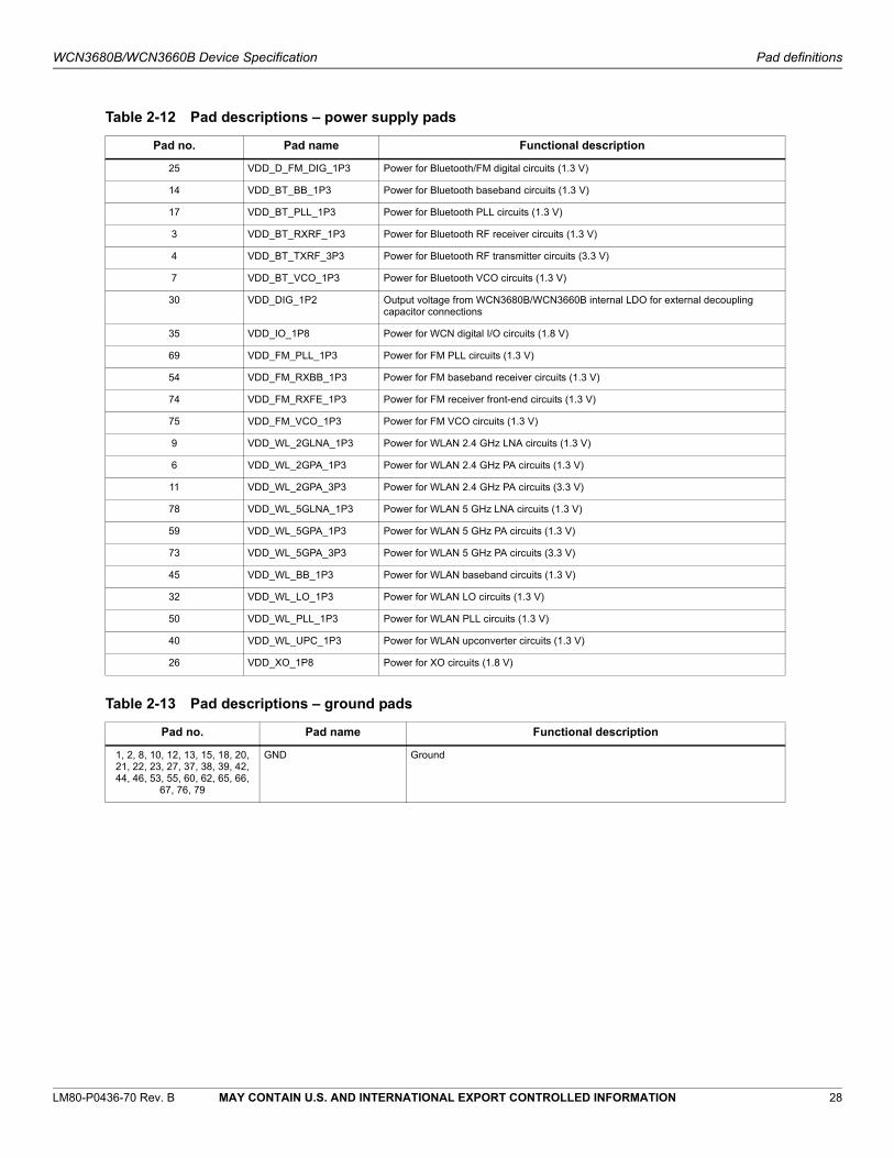
Table 2-12 Pad descriptions – power supply pads
Pad no. Pad name Functional description
25 VDD_D_FM_DIG_1P3 Power for Bluetooth/FM digital circuits (1.3 V)
14 VDD_BT_BB_1P3 Power for Bluetooth baseband circuits (1.3 V)
17 VDD_BT_PLL_1P3 Power for Bluetooth PLL circuits (1.3 V)
3 VDD_BT_RXRF_1P3 Power for Bluetooth RF receiver circuits (1.3 V)
4 VDD_BT_TXRF_3P3 Power for Bluetooth RF transmitter circuits (3.3 V)
7 VDD_BT_VCO_1P3 Power for Bluetooth VCO circuits (1.3 V)
30 VDD_DIG_1P2 Output voltage from WCN3680B/WCN3660B internal LDO for external decoupling capacitor connections
35 VDD_IO_1P8 Power for WCN digital I/O circuits (1.8 V)
69 VDD_FM_PLL_1P3 Power for FM PLL circuits (1.3 V)
54 VDD_FM_RXBB_1P3 Power for FM baseband receiver circuits (1.3 V)
74 VDD_FM_RXFE_1P3 Power for FM receiver front-end circuits (1.3 V)
75 VDD_FM_VCO_1P3 Power for FM VCO circuits (1.3 V)
9 VDD_WL_2GLNA_1P3 Power for WLAN 2.4 GHz LNA circuits (1.3 V)
6 VDD_WL_2GPA_1P3 Power for WLAN 2.4 GHz PA circuits (1.3 V)
11 VDD_WL_2GPA_3P3 Power for WLAN 2.4 GHz PA circuits (3.3 V)
78 VDD_WL_5GLNA_1P3 Power for WLAN 5 GHz LNA circuits (1.3 V)
59 VDD_WL_5GPA_1P3 Power for WLAN 5 GHz PA circuits (1.3 V)
73 VDD_WL_5GPA_3P3 Power for WLAN 5 GHz PA circuits (3.3 V)
45 VDD_WL_BB_1P3 Power for WLAN baseband circuits (1.3 V)
32 VDD_WL_LO_1P3 Power for WLAN LO circuits (1.3 V)
50 VDD_WL_PLL_1P3 Power for WLAN PLL circuits (1.3 V)
40 VDD_WL_UPC_1P3 Power for WLAN upconverter circuits (1.3 V)
26 VDD_XO_1P8 Power for XO circuits (1.8 V)
Table 2-13 Pad descriptions – ground pads
Pad no. Pad name Functional description
1, 2, 8, 10, 12, 13, 15, 18, 20, 21, 22, 23, 27, 37, 38, 39, 42, 44, 46, 53, 55, 60, 62, 65, 66,
67, 76, 79
GND Ground
LM80-P0436-70 Rev. B MAY CONTAIN U.S. AND INTERNATIONAL EXPORT CONTROLLED INFORMATION 29
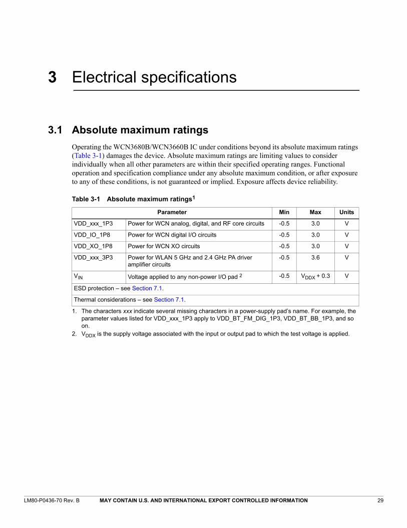
3 Electrical specifications
3.1 Absolute maximum ratings
Operating the WCN3680B/WCN3660B IC under conditions beyond its absolute maximum ratings (Table 3-1) damages the device. Absolute maximum ratings are limiting values to consider individually when all other parameters are within their specified operating ranges. Functional operation and specification compliance under any absolute maximum condition, or after exposure to any of these conditions, is not guaranteed or implied. Exposure affects device reliability.
Table 3-1 Absolute maximum ratings1
1. The characters xxx indicate several missing characters in a power-supply pad’s name. For example, the parameter values listed for VDD_xxx_1P3 apply to VDD_BT_FM_DIG_1P3, VDD_BT_BB_1P3, and so on.
Parameter Min Max Units
VDD_xxx_1P3 Power for WCN analog, digital, and RF core circuits -0.5 3.0 V
VDD_IO_1P8 Power for WCN digital I/O circuits -0.5 3.0 V
VDD_XO_1P8 Power for WCN XO circuits -0.5 3.0 V
VDD_xxx_3P3 Power for WLAN 5 GHz and 2.4 GHz PA driver amplifier circuits
-0.5 3.6 V
VIN Voltage applied to any non-power I/O pad 2
2. VDDX is the supply voltage associated with the input or output pad to which the test voltage is applied.
-0.5 VDDX + 0.3 V
ESD protection – see Section 7.1.
Thermal considerations – see Section 7.1.
LM80-P0436-70 Rev. B MAY CONTAIN U.S. AND INTERNATIONAL EXPORT CONTROLLED INFORMATION 30
WCN3680B/WCN3660B Device Specification Electrical specifications
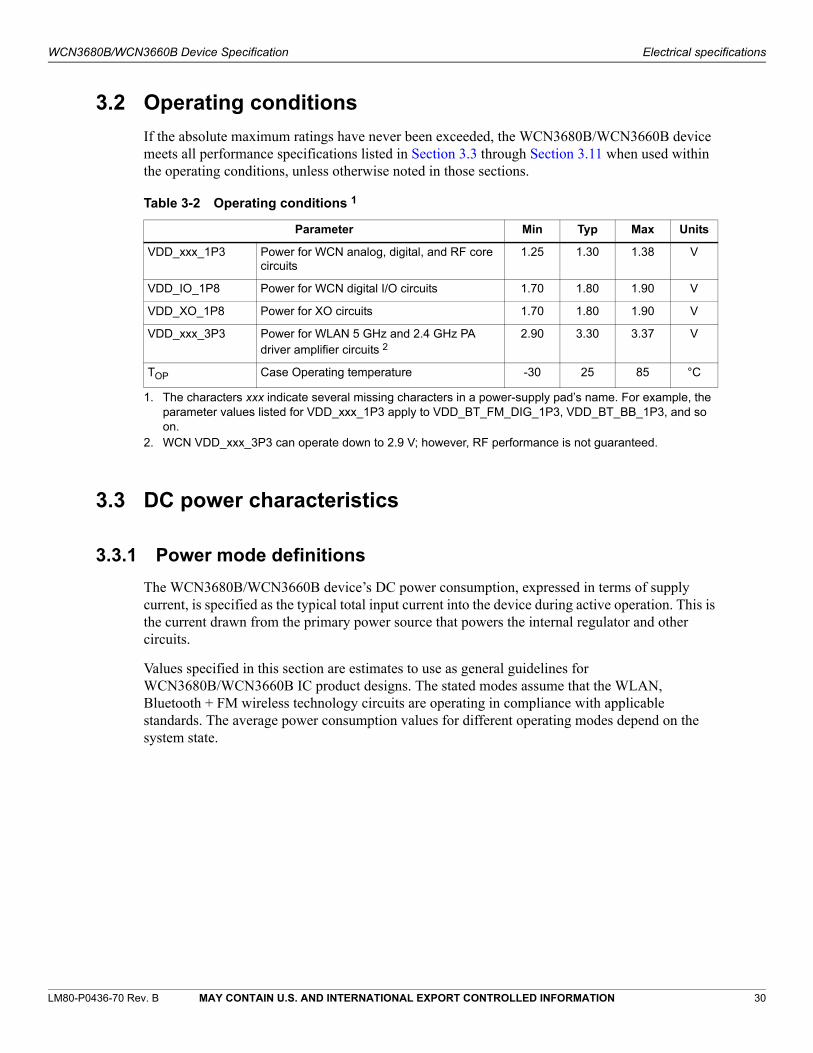
3.2 Operating conditions
If the absolute maximum ratings have never been exceeded, the WCN3680B/WCN3660B device meets all performance specifications listed in Section 3.3 through Section 3.11 when used within the operating conditions, unless otherwise noted in those sections.
3.3 DC power characteristics
3.3.1 Power mode definitions
The WCN3680B/WCN3660B device’s DC power consumption, expressed in terms of supply current, is specified as the typical total input current into the device during active operation. This is the current drawn from the primary power source that powers the internal regulator and other circuits.
Values specified in this section are estimates to use as general guidelines for WCN3680B/WCN3660B IC product designs. The stated modes assume that the WLAN, Bluetooth + FM wireless technology circuits are operating in compliance with applicable standards. The average power consumption values for different operating modes depend on the system state.
Table 3-2 Operating conditions 1
1. The characters xxx indicate several missing characters in a power-supply pad’s name. For example, the parameter values listed for VDD_xxx_1P3 apply to VDD_BT_FM_DIG_1P3, VDD_BT_BB_1P3, and so on.
Parameter Min Typ Max Units
VDD_xxx_1P3 Power for WCN analog, digital, and RF core circuits
1.25 1.30 1.38 V
VDD_IO_1P8 Power for WCN digital I/O circuits 1.70 1.80 1.90 V
VDD_XO_1P8 Power for XO circuits 1.70 1.80 1.90 V
VDD_xxx_3P3 Power for WLAN 5 GHz and 2.4 GHz PA driver amplifier circuits 2
2. WCN VDD_xxx_3P3 can operate down to 2.9 V; however, RF performance is not guaranteed.
2.90 3.30 3.37 V
TOP Case Operating temperature -30 25 85 °C
LM80-P0436-70 Rev. B MAY CONTAIN U.S. AND INTERNATIONAL EXPORT CONTROLLED INFORMATION 31
WCN3680B/WCN3660B Device Specification Electrical specifications
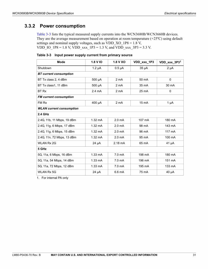
3.3.2 Power consumption
Table 3-3 lists the typical measured supply currents into the WCN3680B/WCN3660B devices. They are the average measurement based on operation at room temperature (+25ºC) using default settings and nominal supply voltages, such as VDD_XO_1P8 = 1.8 V, VDD_IO_1P8 = 1.8 V, VDD_xxx_1P3 = 1.3 V, and VDD_xxx_3P3 = 3.3 V.
Table 3-3 Input power supply current from primary source
Mode 1.8 V IO 1.8 V XO VDD_xxx_1P3 VDD_xxx_3P31
1. For internal PA only
Shutdown 1.2 µA 0.5 µA 35 µA 2 µA
BT current consumption
BT Tx class 2, 4 dBm 500 µA 2 mA 50 mA 0
BT Tx class1, 11 dBm 500 µA 2 mA 35 mA 30 mA
BT Rx 2.4 mA 2 mA 25 mA 0
FM current consumption
FM Rx 400 µA 2 mA 15 mA 1 µA
WLAN current consumption
2.4 GHz
2.4G, 11b, 11 Mbps, 19 dBm 1.32 mA 2.0 mA 107 mA 180 mA
2.4G, 11g, 6 Mbps, 17 dBm 1.32 mA 2.0 mA 98 mA 143 mA
2.4G, 11g, 6 Mbps, 15 dBm 1.32 mA 2.0 mA 96 mA 117 mA
2.4G, 11n, 72 Mbps, 13 dBm 1.32 mA 2.0 mA 95 mA 100 mA
WLAN Rx 2G 24 µA 2.18 mA 65 mA 41 µA
5 GHz
5G, 11a, 6 Mbps, 16 dBm 1.33 mA 7.0 mA 198 mA 180 mA
5G, 11a, 54 Mbps, 14 dBm 1.33 mA 7.0 mA 196 mA 151 mA
5G, 11a, 72 Mbps, 12 dBm 1.33 mA 7.0 mA 195 mA 133 mA
WLAN Rx 5G 24 µA 6.6 mA 75 mA 40 µA
LM80-P0436-70 Rev. B MAY CONTAIN U.S. AND INTERNATIONAL EXPORT CONTROLLED INFORMATION 32
WCN3680B/WCN3660B Device Specification Electrical specifications
3.4 Power sequencing
The WCN3680B/WCN3660B device requires the following powerup sequence:
For APQ8016E: 1.3 V(S3) → 1.8_IO (L5) → 1.8V_XO(L7) → 3.3V_PA (L9)
For all other platforms:
Either VDD_XO_1P8 or VDD_IO_1P8
Either VDD_xxx_1P3 or VDD_xxx_3P3
To power down the device, the following sequence is required:
For APQ8016E: 3.3V_PA (L9) → 1.8V_IO (L5) → 1.8_XO (L7) → 1.3V(S3)
For all other platforms:
VDD_xxx_1P3 and VDD_xxx_3P3
Either VDD_XO_1P8 or VDD_IO_1P8
NOTE If 1.3 V is off before 3.3 V, the interval between 1.3 V off and 3.3 V off must be very short. Any leakage current can be ignored.
3.5 WCN3680B/WCN3660B internal LDO regulatorThe WCN3680B/WCN3660B has an on-chip LDO regulator to provide power supply to the WCN3680B/WCN3660B 1.2 V digital core. The integrated LDO input voltage is applied from the VDD_XO_1P8 voltage. The output pad of this internal LDO is VDD_DIG_1P2 (pad 30). The output at this pad is used to connect decoupling capacitors to reduce supply noise. The WCN3680B/WCN3660B device integrated regulator is intended for use with an on-chip load only. They are not designed to supply external loads.
3.6 Digital logic characteristics
Specifications for the digital I/Os depend on the associated supply voltage (identified as VIO in Table 3-4).
Table 3-4 Baseband digital I/O characteristics
Parameter Comments Min Typ Max Units
VIH High-level input voltage 0.70x VIO – VIO + 0.3 V
VIL Low-level input voltage -0.3x – 0.30 · VIO V
VSHYS Schmitt hysteresis voltage – 300 – mV
IIH Input high leakage current V_IN = VIO max -1.0x – 1.0 µA
IIL Input low leakage current V_IN = 0 V; supply = VIO max -1.0x – 1.0 µA
RPULL Input pull resistor 1 Up or down – 375 k – k
VOH High-level output voltage VIO - 0.4x – VIO V

LM80-P0436-70 Rev. B MAY CONTAIN U.S. AND INTERNATIONAL EXPORT CONTROLLED INFORMATION 33
WCN3680B/WCN3660B Device Specification Electrical specifications
3.7 Timing characteristics
Specifications for the device timing characteristics are included, where appropriate, under each function’s section, along with its other performance specifications. Some general comments about timing characteristics are included here.
NOTE All WCN3680B/WCN3660B devices are characterized with actively terminated loads, so all baseband timing parameters in this document assume no bus loading. This is described in Section 3.7.2.
3.7.1 Timing diagram conventions
Figure 3-1 shows the conventions used within timing diagrams throughout this document.
Figure 3-1 Timing diagram conventions
VOL Low-level output voltage 0 – 0.4 V
IOH High-level output current 1.0 – – mA
IOL Low-level output current – – -1.0 mA
CIN Input capacitance 2 – – 5 pF
1. Resistor values can be increased by 50% when 3.3 V I/O is used.2. Guaranteed by design but not 100% tested.
Table 3-4 Baseband digital I/O characteristics (cont.)
Parameter Comments Min Typ Max Units
Keeper
Don't care or bus is driven.
Signal is changing from low to high.
Signal is changing from high to low.
Bus is changing from invalid to valid.
Bus is changing from valid to keeper.
Waveform Description
Denotes multiple clock periods.
Bus is changing from Hi-Z to valid.

LM80-P0436-70 Rev. B MAY CONTAIN U.S. AND INTERNATIONAL EXPORT CONTROLLED INFORMATION 34
WCN3680B/WCN3660B Device Specification Electrical specifications
3.7.2 Rise and fall time specifications
The testers that characterize WCN3680B/WCN3660B devices have actively terminated loads, making the rise and fall times quicker (mimicking a no-load condition). Figure 3-2 shows the impact that different external load conditions have on rise and fall times.
Figure 3-2 Rise and fall times under different load conditions
To account for external load conditions, rise or fall times must be added to parameters that start timing at the WCN device and terminate at an external device (or vice versa). Adding these rise and fall times is equivalent to applying capacitive load derating factors, and Table 3-5 lists the recommended derating factors.
3.8 Top-level support
3.8.1 I/O block
Modem IC interfaces for WLAN, BT, and FM radio are supported by this block; pertinent specifications are covered within Section 3.6.
Specified switch low points(active terminated load)
Simulated driving30 pF signal load
Actual switch lowpoint at 30 pF
0V
Simulated driving80 pF signal load
0V
VOH
VOL
VOH
VOL
Specified switch high points(active terminated load)
Actual switch highpoint at 30 pF
Actual switch highpoint at 80 pF
Actual switch lowpoint at 80 pF
VDD_PX
VDD_PX
Table 3-5 Capacitive load derating factors
Parameter1.8 V I/O
UnitsDrive = 1.0 mA
Rise time, 10% to 90% 0.29 maximum ns/pF
Fall time, 90% to 10% 0.19 maximum ns/pF

LM80-P0436-70 Rev. B MAY CONTAIN U.S. AND INTERNATIONAL EXPORT CONTROLLED INFORMATION 35
WCN3680B/WCN3660B Device Specification Electrical specifications
3.8.2 Master reference clock requirements
For 2.4 GHz WLAN operation only, the WCN3660B device requires one 19.2 MHz clock signal that can be generated externally (usually by the PMIC), or can be generated by the external 19.2 MHz crystal. This master reference clock (MRC) is the timing source for all operational functions during active modes. When an external source is used, that signal must be AC-coupled into the XO_IN pad.
For single-band operation at 5.0 GHz or dual-band operation at 2.4 and 5.0 GHz, the WCN3680B/WCN3660B device requires a 48.0 MHz clock from an external crystal. This clock signal is required due to more stringent phase noise requirements when operating the device at 5.0 GHz.
Table 3-6 lists the requirements for operation at 5.0 GHz only or operation at both 2.4 GHz and 5.0 GHz (MRC = 48 MHz).
1. 24 MHz clock on pad 36 (CLK_OUT) is a divide-by-2 version of the 48 MHz XTAL ref clock. An external circuit can be used to reduce the clock swing to 0.4 Vpp for special use case.
3.8.3 DC power gating and distribution
See Section 3.3 and Section 3.4.
Table 3-6 Reference requirements
Parameter Condition Min Typ Max Units
19.2 MHz TCXO
Output frequency – 19.2 – MHz
Frequency variation over temperature/aging
-20 – 20 ppm
Duty cycle of output signal
43.5 50 55 %
Voltage swing 0.8 – 2.0 Vpp
Output phase noise f = 1 kHz – -130 -128 dBc/Hz
f = 10 kHz – -144 -142 dBc/Hz
f = 100 kHz – -151 -148 dBc/Hz
f = 1 MHz – -152 -150 dBc/Hz
Output spur specification – – -30 dBc
48 MHz XTAL – See 48 MHz Crystal for 5 GHz WLAN Connectivity Products Mini-Specification (80-N8644-2) for the WCN3680B/WCN3660B 48 MHz crystal mini-specifications.
48 MHz XO
Operating frequency – 48 – MHz
24 MHz CLK_OUT Operating frequency – 24 – MHz
Voltage swing – 1.81 – Vpp
LM80-P0436-70 Rev. B MAY CONTAIN U.S. AND INTERNATIONAL EXPORT CONTROLLED INFORMATION 36
WCN3680B/WCN3660B Device Specification Electrical specifications
3.9 WLAN RF circuits
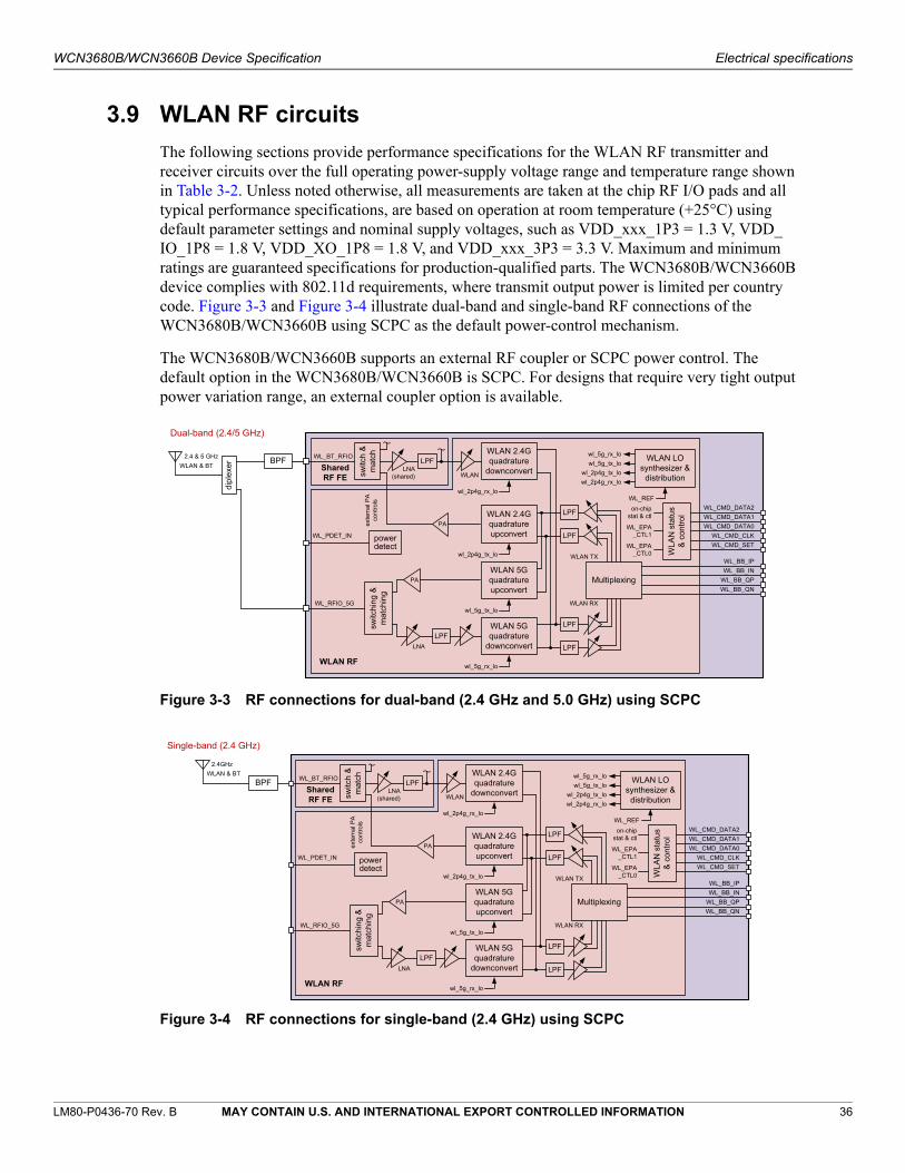
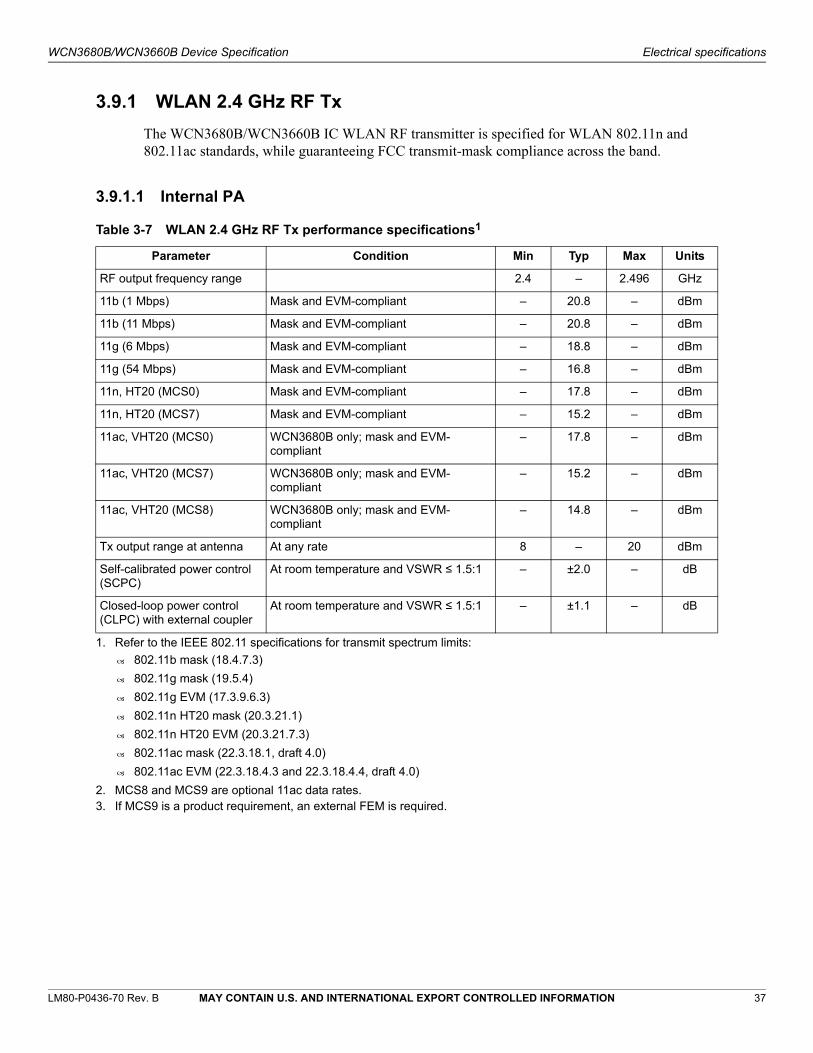
The following sections provide performance specifications for the WLAN RF transmitter and receiver circuits over the full operating power-supply voltage range and temperature range shown in Table 3-2. Unless noted otherwise, all measurements are taken at the chip RF I/O pads and all typical performance specifications, are based on operation at room temperature (+25°C) using default parameter settings and nominal supply voltages, such as VDD_xxx_1P3 = 1.3 V, VDD_IO_1P8 = 1.8 V, VDD_XO_1P8 = 1.8 V, and VDD_xxx_3P3 = 3.3 V. Maximum and minimum ratings are guaranteed specifications for production-qualified parts. The WCN3680B/WCN3660B device complies with 802.11d requirements, where transmit output power is limited per country code. Figure 3-3 and Figure 3-4 illustrate dual-band and single-band RF connections of the WCN3680B/WCN3660B using SCPC as the default power-control mechanism.
The WCN3680B/WCN3660B supports an external RF coupler or SCPC power control. The default option in the WCN3680B/WCN3660B is SCPC. For designs that require very tight output power variation range, an external coupler option is available.
Figure 3-3 RF connections for dual-band (2.4 GHz and 5.0 GHz) using SCPC
Figure 3-4 RF connections for single-band (2.4 GHz) using SCPC
WL_BB_IPWL_BB_IN
WL_BB_QPWL_BB_QN
WL_CMD_DATA1WL_CMD_DATA0
WL_CMD_CLKWL_CMD_SET
WL_CMD_DATA2
Dual-band (2.4/5 GHz)
WLAN LOsynthesizer &
distribution
LPF
LPF
WLAN 2.4Gquadrature
downconvert
LPF
LPFWLAN 2.4Gquadratureupconvert
wl_2p4g_tx_lo
Multiplexing
SharedRF FE
WLAN 5Gquadratureupconvert
wl_5g_tx_lo
WLAN TX
WLAN RX
WLA
Nst
atus
&co
ntro
l
on-chipstat & ctl
switc
h&
mat
ch
wl_2p4g_rx_lo
WLAN 5Gquadrature
downconvert
wl_5g_rx_lo
WL_EPA_CTL1
WL_EPA_CTL0
wl_5g_rx_lowl_5g_tx_lo
wl_2p4g_tx_lowl_2p4g_rx_lo
WL_REF
powerdetect
WL_BT_RFIO
PA
LNA(shared)
WLAN RF
WLAN
switc
hing
&m
atch
ing
LNA
PA
WL_RFIO_5G
exte
rnal
PA
cont
rols
LPF
LPF
WLAN & BT2.4 & 5 GHz BPF
dipl
exer
WL_PDET_IN
WL_BB_IPWL_BB_IN
WL_BB_QPWL_BB_QN
WL_CMD_DATA1WL_CMD_DATA0
WL_CMD_CLKWL_CMD_SET
WL_CMD_DATA2
Single-band (2.4 GHz)
WLAN LOsynthesizer &
distribution
LPF
LPF
WLAN 2.4Gquadrature
downconvert
LPF
LPFWLAN 2.4Gquadratureupconvert
wl_2p4g_tx_lo
Multiplexing
SharedRF FE
WLAN 5Gquadratureupconvert
wl_5g_tx_lo
WLAN TX
WLAN RX
WLA
Nst
atus
&co
ntro
l
on-chipstat & ctl
switc
h&
mat
ch
wl_2p4g_rx_lo
WLAN 5Gquadrature
downconvert
wl_5g_rx_lo
WL_EPA_CTL1
WL_EPA_CTL0
wl_5g_rx_lowl_5g_tx_lo
wl_2p4g_tx_lowl_2p4g_rx_lo
WL_REF
powerdetect
WL_BT_RFIO
PA
LNA(shared)
WLAN RF
WLAN
switc
hing
&m
atch
ing
LNA
PA
WL_RFIO_5G
exte
rnal
PA
cont
rols
LPF
LPF
WLAN & BT2.4GHz
BPF
WL_PDET_IN
LM80-P0436-70 Rev. B MAY CONTAIN U.S. AND INTERNATIONAL EXPORT CONTROLLED INFORMATION 37
WCN3680B/WCN3660B Device Specification Electrical specifications
3.9.1 WLAN 2.4 GHz RF Tx
The WCN3680B/WCN3660B IC WLAN RF transmitter is specified for WLAN 802.11n and 802.11ac standards, while guaranteeing FCC transmit-mask compliance across the band.
3.9.1.1 Internal PA
Table 3-7 WLAN 2.4 GHz RF Tx performance specifications1
1. Refer to the IEEE 802.11 specifications for transmit spectrum limits:
802.11b mask (18.4.7.3)
802.11g mask (19.5.4)
802.11g EVM (17.3.9.6.3)
802.11n HT20 mask (20.3.21.1)
802.11n HT20 EVM (20.3.21.7.3)
802.11ac mask (22.3.18.1, draft 4.0)
802.11ac EVM (22.3.18.4.3 and 22.3.18.4.4, draft 4.0)
2. MCS8 and MCS9 are optional 11ac data rates.3. If MCS9 is a product requirement, an external FEM is required.
Parameter Condition Min Typ Max Units
RF output frequency range 2.4 – 2.496 GHz
11b (1 Mbps) Mask and EVM-compliant – 20.8 – dBm
11b (11 Mbps) Mask and EVM-compliant – 20.8 – dBm
11g (6 Mbps) Mask and EVM-compliant – 18.8 – dBm
11g (54 Mbps) Mask and EVM-compliant – 16.8 – dBm
11n, HT20 (MCS0) Mask and EVM-compliant – 17.8 – dBm
11n, HT20 (MCS7) Mask and EVM-compliant – 15.2 – dBm
11ac, VHT20 (MCS0) WCN3680B only; mask and EVM-compliant
– 17.8 – dBm
11ac, VHT20 (MCS7) WCN3680B only; mask and EVM-compliant
– 15.2 – dBm
11ac, VHT20 (MCS8) WCN3680B only; mask and EVM-compliant
– 14.8 – dBm
Tx output range at antenna At any rate 8 – 20 dBm
Self-calibrated power control (SCPC)
At room temperature and VSWR ≤ 1.5:1 – ±2.0 – dB
Closed-loop power control (CLPC) with external coupler
At room temperature and VSWR ≤ 1.5:1 – ±1.1 – dB
LM80-P0436-70 Rev. B MAY CONTAIN U.S. AND INTERNATIONAL EXPORT CONTROLLED INFORMATION 38
WCN3680B/WCN3660B Device Specification Electrical specifications
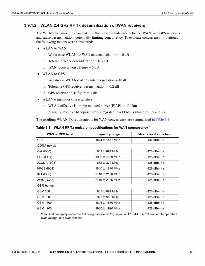
3.9.1.2 WLAN 2.4 GHz RF Tx desensitization of WAN receivers
The WLAN transmissions can leak into the device’s wide area network (WAN) and GPS receivers and cause desensitization, potentially limiting concurrency. To evaluate concurrency limitations, the following factors were considered:
WLAN to WAN
Worst-case WLAN-to-WAN antenna isolation = 10 dB
Tolerable WAN desensitization = 0.3 dB
WAN receiver noise figure = 6 dB
WLAN to GPS
Worst-case WLAN-to-GPS antenna isolation = 10 dB
Tolerable GPS receiver desensitization = 0.2 dB
GPS receiver noise figure = 3 dB
WLAN transmitter characteristics
WLAN effective isotropic radiated power (EIRP) = 15 dBm
A highly selective bandpass filter (integrated in a FEM) is shared by Tx and Rx
The resulting WLAN Tx requirements for WAN concurrency are summarized in Table 3-8.
Table 3-8 WLAN RF Tx emission specifications for WAN concurrency 1
1. Specifications apply under the following conditions: 11g signal at 17.5 dBm, 45°C ambient temperature, over voltage, and over process.
WAN or GPS band Frequency range Max Tx level in Rx band
GPS 1574 to 1577 MHz -136 dBm/Hz
CDMA bands
Cell (BC0) 869 to 894 MHz -128 dBm/Hz
PCS (BC1) 1930 to 1990 MHz -128 dBm/Hz
JCDMA (BC3) 832 to 870 MHz -128 dBm/Hz
KPCS (BC4) 1840 to 1870 MHz -128 dBm/Hz
IMT (BC6) 2110 to 2170 MHz -128 dBm/Hz
AWS (BC15) 2110 to 2155 MHz -128 dBm/Hz
GSM bands
GSM 850 869 to 894 MHz -128 dBm/Hz
GSM 900 925 to 960 MHz -128 dBm/Hz
GSM 1800 1805 to 1880 MHz -128 dBm/Hz
GSM 1900 1930 to 1990 MHz -128 dBm/Hz
WCN3680B/WCN3660B Device Specification Electrical specifications
LM80-P0436-70 Rev. B MAY CONTAIN U.S. AND INTERNATIONAL EXPORT CONTROLLED INFORMATION 39
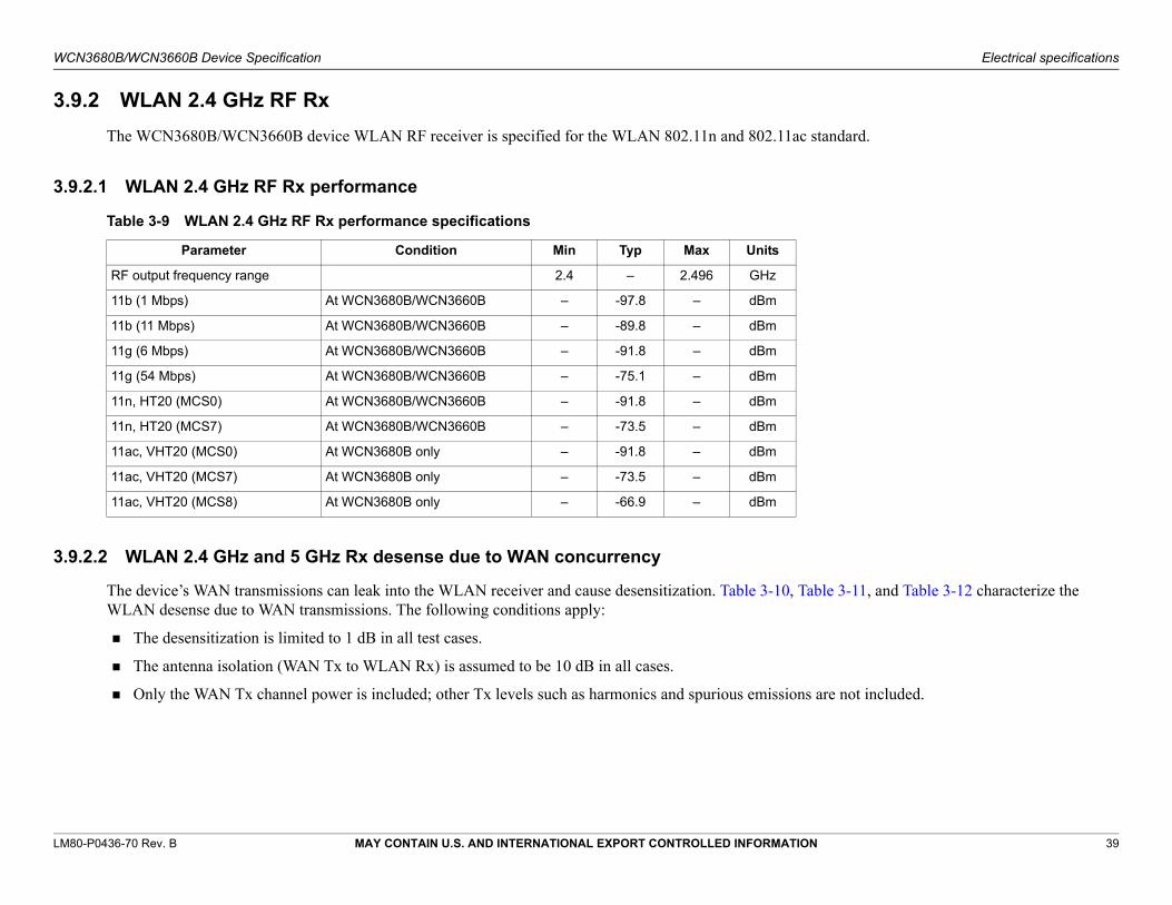
3.9.2 WLAN 2.4 GHz RF Rx
The WCN3680B/WCN3660B device WLAN RF receiver is specified for the WLAN 802.11n and 802.11ac standard.
3.9.2.1 WLAN 2.4 GHz RF Rx performance
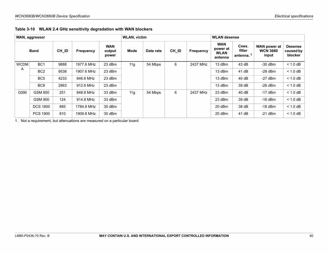
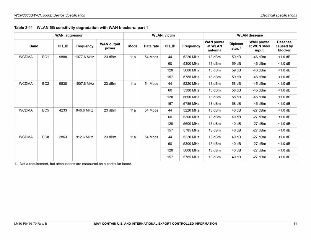
3.9.2.2 WLAN 2.4 GHz and 5 GHz Rx desense due to WAN concurrency
The device’s WAN transmissions can leak into the WLAN receiver and cause desensitization. Table 3-10, Table 3-11, and Table 3-12 characterize the WLAN desense due to WAN transmissions. The following conditions apply:
The desensitization is limited to 1 dB in all test cases.
The antenna isolation (WAN Tx to WLAN Rx) is assumed to be 10 dB in all cases.
Only the WAN Tx channel power is included; other Tx levels such as harmonics and spurious emissions are not included.
Table 3-9 WLAN 2.4 GHz RF Rx performance specifications
Parameter Condition Min Typ Max Units
RF output frequency range 2.4 – 2.496 GHz
11b (1 Mbps) At WCN3680B/WCN3660B – -97.8 – dBm
11b (11 Mbps) At WCN3680B/WCN3660B – -89.8 – dBm
11g (6 Mbps) At WCN3680B/WCN3660B – -91.8 – dBm
11g (54 Mbps) At WCN3680B/WCN3660B – -75.1 – dBm
11n, HT20 (MCS0) At WCN3680B/WCN3660B – -91.8 – dBm
11n, HT20 (MCS7) At WCN3680B/WCN3660B – -73.5 – dBm
11ac, VHT20 (MCS0) At WCN3680B only – -91.8 – dBm
11ac, VHT20 (MCS7) At WCN3680B only – -73.5 – dBm
11ac, VHT20 (MCS8) At WCN3680B only – -66.9 – dBm
WCN3680B/WCN3660B Device Specification Electrical specifications
LM80-P0436-70 Rev. B MAY CONTAIN U.S. AND INTERNATIONAL EXPORT CONTROLLED INFORMATION 40
Table 3-10 WLAN 2.4 GHz sensitivity degradation with WAN blockers
WAN, aggressor WLAN, victim WLAN desense
Band CH_ID FrequencyWAN
output power
Mode Data rate CH_ID Frequency
WAN power at WLAN
antenna
Coex. filter
antenna. 1
1. Not a requirement, but attenuations are measured on a particular board.
WAN power at WCN 3660
input
Desense caused by
blocker
WCDMA
BC1 9888 1977.6 MHz 23 dBm 11g 54 Mbps 6 2437 MHz 13 dBm 43 dB -30 dBm < 1.0 dB
BC2 9538 1907.6 MHz 23 dBm 13 dBm 41 dB -28 dBm < 1.0 dB
BC5 4233 846.6 MHz 23 dBm 13 dBm 40 dB -27 dBm < 1.0 dB
BC8 2863 912.6 MHz 23 dBm 13 dBm 39 dB -26 dBm < 1.0 dB
GSM GSM 850 251 848.8 MHz 33 dBm 11g 54 Mbps 6 2437 MHz 23 dBm 40 dB -17 dBm < 1.0 dB
GSM 900 124 914.8 MHz 33 dBm 23 dBm 39 dB -16 dBm < 1.0 dB
DCS 1800 885 1784.8 MHz 30 dBm 20 dBm 38 dB -18 dBm < 1.0 dB
PCS 1900 810 1909.8 MHz 30 dBm 20 dBm 41 dB -21 dBm < 1.0 dB
WCN3680B/WCN3660B Device Specification Electrical specifications
LM80-P0436-70 Rev. B MAY CONTAIN U.S. AND INTERNATIONAL EXPORT CONTROLLED INFORMATION 41
Table 3-11 WLAN 5G sensitivity degradation with WAN blockers: part 1
WAN, aggressor WLAN, victim WLAN desense
Band CH_ID FrequencyWAN output
powerMode Data rate CH_ID Frequency
WAN power at WLAN antenna
Diplexer attn. 1
1. Not a requirement, but attenuations are measured on a particular board.
WAN power at WCN 3660
input
Desense caused by
blocker
WCDMA BC1 9888 1977.6 MHz 23 dBm 11a 54 Mbps 44 5220 MHz 13 dBm 59 dB -46 dBm <1.0 dB
60 5300 MHz 13 dBm 59 dB -46 dBm <1.0 dB
120 5600 MHz 13 dBm 59 dB -46 dBm <1.0 dB
157 5785 MHz 13 dBm 59 dB -46 dBm <1.0 dB
WCDMA BC2 9538 1907.6 MHz 23 dBm 11a 54 Mbps 44 5220 MHz 13 dBm 58 dB -45 dBm <1.0 dB
60 5300 MHz 13 dBm 58 dB -45 dBm <1.0 dB
120 5600 MHz 13 dBm 58 dB -45 dBm <1.0 dB
157 5785 MHz 13 dBm 58 dB -45 dBm <1.0 dB
WCDMA BC5 4233 846.6 MHz 23 dBm 11a 54 Mbps 44 5220 MHz 13 dBm 40 dB -27 dBm <1.0 dB
60 5300 MHz 13 dBm 40 dB -27 dBm <1.0 dB
120 5600 MHz 13 dBm 40 dB -27 dBm <1.0 dB
157 5785 MHz 13 dBm 40 dB -27 dBm <1.0 dB
WCDMA BC8 2863 912.6 MHz 23 dBm 11a 54 Mbps 44 5220 MHz 13 dBm 40 dB -27 dBm <1.0 dB
60 5300 MHz 13 dBm 40 dB -27 dBm <1.0 dB
120 5600 MHz 13 dBm 40 dB -27 dBm <1.0 dB
157 5785 MHz 13 dBm 40 dB -27 dBm <1.0 dB

WCN3680B/WCN3660B Device Specification Electrical specifications
LM80-P0436-70 Rev. B MAY CONTAIN U.S. AND INTERNATIONAL EXPORT CONTROLLED INFORMATION 42
Table 3-12 WLAN 5G sensitivity degradation with WAN blockers - Part 2
WAN, aggressor WLAN, victim WLAN desense
Band CH_ID FrequencyWAN
output power
Mode Data rate CH_ID FrequencyWAN power
at WLAN antenna
Diplexer attn. 1
1. Not a requirement, but attenuations measured on a particular board.
WAN power at WCN
3660 input
Desense caused by
blocker
GSM GSM 850 251 848.8 MHz 33 dBm 11a 54 Mbps 44 5220 MHz 23 dBm 40 dB -17 dBm <1.0 dB
60 5300 MHz 23 dBm 40 dB -17 dBm <1.0 dB
120 5600 MHz 23 dBm 40 dB -17 dBm <1.0 dB
157 5785 MHz 23 dBm 40 dB -17 dBm <1.0 dB
GSM GSM 900 124 914.8 MHz 33 dBm 11a 54 Mbps 44 5220 MHz 23 dBm 40 dB -17 dBm <1.0 dB
60 5300 MHz 23 dBm 40 dB -17 dBm <1.0 dB
120 5600 MHz 23 dBm 40 dB -17 dBm <1.0 dB
157 5785 MHz 23 dBm 40 dB -17 dBm <1.0 dB
GSM DCS 1800 885 1784.8 MHz
30 dBm 11a 54 Mbps 44 5220 MHz 20 dBm 55 dB -35 dBm <1.0 dB
60 5300 MHz 20 dBm 55 dB -35 dBm <1.0 dB
120 5600 MHz 20 dBm 55 dB -35 dBm <1.0 dB
157 5785 MHz 20 dBm 55 dB -35 dBm <1.0 dB
GSM PCS 1900 810 1909.8 MHz
30 dBm 11a 54 Mbps 44 5220 MHz 20 dBm 59 dB -39 dBm <1.0 dB
60 5300 MHz 20 dBm 59 dB -39 dBm <1.0 dB
120 5600 MHz 20 dBm 59 dB -39 dBm <1.0 dB
157 5785 MHz 20 dBm 59 dB -39 dBm <1.0 dB

LM80-P0436-70 Rev. B MAY CONTAIN U.S. AND INTERNATIONAL EXPORT CONTROLLED INFORMATION 43
WCN3680B/WCN3660B Device Specification Electrical specifications
3.9.3 WLAN 5 GHz RF Tx
The WCN3680B/WCN3660B IC RF transmitter integrates a 5 GHz power amplifier designed to comply with FCC transmit-mask and mandatory EVM levels defined in 802.11n and 802.11ac (WCN3680-only) IEEE standards.
The WCN3680B/WCN3660B IC also supports the use of an external 2.4 GHz and 5 GHz PA for applications requiring higher transmit power.
3.9.3.1 Internal PA
Table 3-13 WLAN 5 GHz RF Tx performance specifications 1
Parameter Condition Min Typ Max Units
RF output frequency range 4.9 - 5.85 GHz
11a (6 Mbps) Mask and EVM-compliant – 17.6 – dBm
11a (54 Mbps) Mask and EVM-compliant – 15.6 – dBm
11n, HT20 (MCS0) Mask and EVM-compliant – 16.6 – dBm
11n, HT20 (MCS7) Mask and EVM-compliant – 14.6 – dBm
11n, HT40 (MCS0) Mask and EVM-compliant – 15.6 – dBm
11n, HT40 (MCS7) Mask and EVM-compliant – 13.6 – dBm
11ac, VHT20 (MCS0) WCN3680B only; mask and EVM-compliant – 16.6 – dBm
11ac, VHT20 (MCS7) WCN3680B only; mask and EVM-compliant – 14.6 – dBm
11ac, VHT20 (MCS8 2) WCN3680B only; mask and EVM-compliant – 13.6 – dBm
11ac, VHT40 (MCS0) WCN3680B only; mask and EVM-compliant – 15.6 – dBm
11ac, VHT40 (MCS7) WCN3680B only; mask and EVM-compliant – 13.6 – dBm
11ac, VHT40 (MCS8 2) WCN3680B only; mask and EVM-compliant – 12.6 – dBm
11ac, VHT80 (MCS0) WCN3680B only; mask and EVM-compliant – 14.6 – dBm
11ac, VHT80 (MCS7) WCN3680B only; mask and EVM-compliant – 12.6 – dBm
11ac, VHT80 (MCS8 2) WCN3680B only; mask and EVM-compliant – 11.6 – dBm
Tx output range at antenna At any rate 8 – 20 dBm
Self-calibrated power control (SCPC)
At room temperature and VSWR ≤ 1.5:1 – ±2.0 – dB
Closed-loop power control (CLPC) with external coupler
At room temperature and VSWR ≤ 1.5:1 – ±1.1 – dB
1. MCS9 is an optional 11ac data rate. If MCS9 is a product requirement, use the external FEM.2. MCS8 is an optional 11ac data rate.
LM80-P0436-70 Rev. B MAY CONTAIN U.S. AND INTERNATIONAL EXPORT CONTROLLED INFORMATION 44
WCN3680B/WCN3660B Device Specification Electrical specifications
3.9.3.2 External PA
For applications requiring higher transmit power in the 2.4 GHz and 5 GHz bands, the WCN3680B/WCN3660B device supports the option for an external PA for 2.4 GHz and 5 GHz paths. In this configuration, the WCN digital amplifier output is routed to pad 47 to bypass the internal PA. If using an external PA for 5G, the WL_RFIO_5G pad 72 is set to Rx mode only, and if using an external PA for 2G, the WL_BT_RFIO_2P4G pad 5 is set to WLAN Rx 2.4 GHz and BT Tx/Rx paths. The internal PAs are turned off to allow external front-end modules (FEM) to be used as the primary 2G and 5G amplifiers.
By using external FEMs for the 2G and 5G paths, WCN3660B Wi-Fi performance achieves higher output power than the internal PA case. For WCN3680B, using an external FEM achieves compliance with the MCS9 data rates per the IEEE 802.11ac specification. In addition to the modified 2G and 5G RF configuration, the WCN device also enables five RF control pads, depending on which bands have an external FEM enabled. These pads are WL_EXTPA_CTRL0 (pad 52), WL_EXTPA_CTRL1 (pad 34) for 5 GHz FEM control, and WL_EXTPA_CTRL2 (pad 49), WL_EXTPA_CTRL3 (pad 68), and WL_EXTPA_CTRL4 (pad 56) for 2.4 GHz FEM control. All of these pads are sourced from the 5G PA supply voltage. Each of the five pads is intended to be used as a control line for the front-end hardware and to have software-configurable polarity.

LM80-P0436-70 Rev. B MAY CONTAIN U.S. AND INTERNATIONAL EXPORT CONTROLLED INFORMATION 45
WCN3680B/WCN3660B Device Specification Electrical specifications
Figure 3-5 RF switch control for dual-band external 2nd generation FEMs
P#49
P#56
P#5
P#72
P#47
P#52
P#68WL_EXTPA_CTRL_3
2G/5G Tx
5G Rx
WL_EXTPA_CTRL_2
WL_EXTPA_CTRL_4
WL_BT_RX_2G
P#34 WL_EXTPA_CTRL_1
WCN3660B/WCN3680B
PA_ENSW_CTL
LNA_EN
5G FEM
2G FEM
CTL2CTL1
SPDT
CTL2CTL1
SPDT
5G Tx
2G Tx
5G Tx/Rx
2G Rx
BT Tx/Rx
C_BTLNA_EN
C_RX PA_EN
2G Tx/Rx + BT
Diplexer
WL_EXTPA_CTRL_0
LPF
Mode WL_EXTPA_CTRL_0 WL_EXTPA_CTRL_1 WL_EXTPA_CTRL_2 WL_EXTPA_CTRL_3 WL_EXTPA_CTRL_4
Off Low Low Low Low LowTX2G Low Low Low High LowRX2G Low Low Low Low HighBluetooth Low Low High Low LowTX5G High Low Low Low LowRX5G Low High Low Low LowTX5G+BT High Low High Low LowRX5G+BT Low High High Low Low
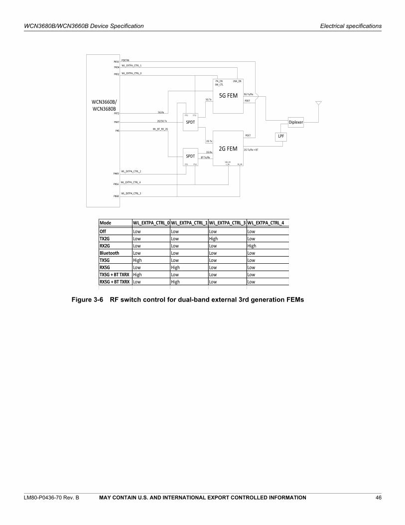
LM80-P0436-70 Rev. B MAY CONTAIN U.S. AND INTERNATIONAL EXPORT CONTROLLED INFORMATION 46
WCN3680B/WCN3660B Device Specification Electrical specifications
Figure 3-6 RF switch control for dual-band external 3rd generation FEMs
P#49
P#56
P#5
P#72
P#47
P#52
P#68WL_EXTPA_CTRL_3
2G/5G Tx
5G Rx
WL_EXTPA_CTRL_2
WL_EXTPA_CTRL_4
WL_BT_RX_2G
P#34 WL_EXTPA_CTRL_1
WCN3660B/WCN3680B
PA_ENSW_CTL
LNA_EN
5G FEM
2G FEM
CTL2CTL1
SPDT
CTL2CTL1
SPDT
5G Tx
2G Tx
5G Tx/Rx
2G Rx
BT Tx/RxLNA_EN
C_RX PA_EN
2G Tx/Rx + BT
WL_EXTPA_CTRL_0
LPF
Mode WL_EXTPA_CTRL_0 WL_EXTPA_CTRL_1 WL_EXTPA_CTRL_3 WL_EXTPA_CTRL_4
Off Low Low Low LowTX2G Low Low High LowRX2G Low Low Low HighBluetooth Low Low Low LowTX5G High Low Low LowRX5G Low High Low LowTX5G + BT TXRX High Low Low LowRX5G + BT TXRX Low High Low Low
Diplexer
PDET
PDET
PDETINP#16

LM80-P0436-70 Rev. B MAY CONTAIN U.S. AND INTERNATIONAL EXPORT CONTROLLED INFORMATION 47
WCN3680B/WCN3660B Device Specification Electrical specifications
Figure 3-7 RF switch control for 2nd generation 5 GHz-only external FEMs
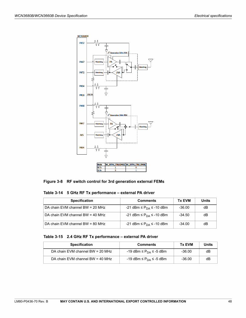
LM80-P0436-70 Rev. B MAY CONTAIN U.S. AND INTERNATIONAL EXPORT CONTROLLED INFORMATION 48
WCN3680B/WCN3660B Device Specification Electrical specifications
Figure 3-8 RF switch control for 3rd generation external FEMs
Table 3-14 5 GHz RF Tx performance – external PA driver
Specification Comments Tx EVM Units
DA chain EVM channel BW = 20 MHz -21 dBm ≤ PDA ≤ -10 dBm -36.00 dB
DA chain EVM channel BW = 40 MHz -21 dBm ≤ PDA ≤ -10 dBm -34.50 dB
DA chain EVM channel BW = 80 MHz -21 dBm ≤ PDA ≤ -10 dBm -34.00 dB
Table 3-15 2.4 GHz RF Tx performance – external PA driver
Specification Comments Tx EVM Units
DA chain EVM channel BW = 20 MHz -19 dBm ≤ PDA ≤ -5 dBm -36.00 dB
DA chain EVM channel BW = 40 MHz -19 dBm ≤ PDA ≤ -5 dBm -36.00 dB

LM80-P0436-70 Rev. B MAY CONTAIN U.S. AND INTERNATIONAL EXPORT CONTROLLED INFORMATION 49
WCN3680B/WCN3660B Device Specification Electrical specifications
3.9.4 WLAN 5 GHz RF Rx
The WCN3680B/WCN3660B device WLAN RF receiver is specified for the WLAN 802.11n standard.
3.9.5 WLAN analog interface between host and WCN3680B/WCN3660B
The analog interface signals between the WLAN digital baseband of the wireless connectivity subsystem (WCS) in the host and WCN3680 devices are listed in Table 3-17. The I/Q baseband analog interface consists of four transmission lines shared between the Tx and Rx paths. In Tx mode these four lines are used to connect DAC output pads to Tx BBF input pads; the ADC input pads and Rx BBF output pads are in high-Z mode. For Rx mode, conversely, the four lines are used to connect the Rx BBF output pads to ADC input pads as the DAC outputs and Tx BBF inputs are in high-Z mode.
Table 3-16 5 GHz/20 MHz RF performance – Rx sensitivity
Parameter Condition Min Typ Max Units
RF input frequency range 4.9 – 5.85 GHz
11a (6 Mbps) At WCN3680B/WCN3660B WL_BT_RFIO_5G port – -90.6 – dBm
11a (54 Mbps) At WCN3680B/WCN3660B WL_BT_RFIO_5G port – -75.6 – dBm
11n, HT20 (MCS0) At WCN3680B/WCN3660B WL_BT_RFIO_5G port – -89.6 – dBm
11n, HT20 (MCS7) At WCN3680B/WCN3660B WL_BT_RFIO_5G port – -74.0 – dBm
11n, HT40 (MCS0) At WCN3680B/WCN3660B WL_BT_RFIO_5G port – -87.6 – dBm
11n, HT40 (MCS7) At WCN3680B/WCN3660B WL_BT_RFIO_5G port – -71.0 – dBm
11ac, VHT20 (MCS0) At WCN3680B WL_BT_RFIO_5G port – -89.6 – dBm
11ac, VHT20 (MCS7) At WCN3680B WL_BT_RFIO_5G port – -74.0 – dBm
11ac, VHT20 (MCS8) At WCN3680B WL_BT_RFIO_5G port – -68.6 – dBm
11ac, VHT40 (MCS0) At WCN3680B WL_BT_RFIO_5G port – -87.6 – dBm
11ac, VHT40 (MCS7) At WCN3680B WL_BT_RFIO_5G port – -71.0 – dBm
11ac, VHT40 (MCS8) At WCN3680B WL_BT_RFIO_5G port – -64.6 – dBm
11ac, VHT40 (MCS9) At WCN3680B WL_BT_RFIO_5G port – -63.6 – dBm
11ac, VHT80 (MCS0) At WCN3680B WL_BT_RFIO_5G port – -85.6 – dBm
11ac, VHT80 (MCS7) At WCN3680B WL_BT_RFIO_5G port – -66.1 – dBm
11ac, VHT80 (MCS8) At WCN3680B WL_BT_RFIO_5G port – -60.6 – dBm
11ac, VHT80 (MCS9) At WCN3680B WL_BT_RFIO_5G port – -59.6 – dBm

LM80-P0436-70 Rev. B MAY CONTAIN U.S. AND INTERNATIONAL EXPORT CONTROLLED INFORMATION 50
WCN3680B/WCN3660B Device Specification Electrical specifications
The electrical specifications of the interface signals can be found in Table 3-18.
Table 3-17 Analog interface signals
Signal nameDirection (with respect
to RF)Description
WL_BB_IN Analog I/O Baseband analog I negative, multiplexed between TX_IN and RX_IN on the RF side. See Table 3-18.
WL_BB_IP Analog I/O Baseband analog I positive, multiplexed between TX_IP and RX_IP on the RF side. See Table 3-18.
WL_BB_QN Analog I/O Baseband analog Q negative, multiplexed between TX_QN and RX_QN on the RF side. See Table 3-18.
WL_BB_QP Analog I/O Baseband analog Q positive, multiplexed between TX_QP and RX_QP on the RF side. See Table 3-18.
Table 3-18 Analog I/Q interface specifications
Specification Comments Min Typ Max Units
Tx mode operation
Tx I or Q input impedance for normal operation mode, single-ended
DC to 45 MHz – 15 || 1 pF
–
Tx I or Q input impedance for high-Z mode, single-ended
DC to 45 MHz – >1 M || < 2 pF
–
Maximum interconnect capacitance I or Q, single-ended 1
External parasitic capacitance on I or Q inputs due to board routing, connector, etc.
– – 7 pF
Amplitude droop in normal operation mode
At 45 MHz, due to Tx I or Q input impedance parasitic capacitance
– – 0.1 dB
Mean I/Q phase imbalance Measured up to 45 MHz -0.2 – 0.2 Degree
Mean I/Q amplitude imbalance Measured up to 45 MHz -0.5 – 0.5 %
Tx mode, AC current positive or negative inputs (I or Q)
– 250 – µApp
Tx mode, common mode voltage on either positive or negative input (I or Q)
– 0.3 – V
Rx mode operation
Single-ended output impedance for normal operation (I or Q)
DC to 45 MHz – 80 –
Single-ended output impedance for high-Z mode (I or Q)
DC to 45 MHz – >1 M || < 2 pF
–
Rx I/Q output voltage range 0 – 1.6 Vpp
Amplitude droop in normal operation mode
At 45 MHz, due to Rx I or Q output impedance parasitic capacitance
– – 0.1 dB
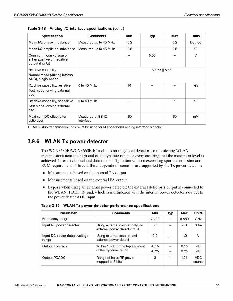
LM80-P0436-70 Rev. B MAY CONTAIN U.S. AND INTERNATIONAL EXPORT CONTROLLED INFORMATION 51
WCN3680B/WCN3660B Device Specification Electrical specifications
3.9.6 WLAN Tx power detector
The WCN3680B/WCN3660B IC includes an integrated detector for monitoring WLAN transmissions near the high end of its dynamic range, thereby ensuring that the maximum level is achieved for each channel and data-rate configuration without exceeding spurious emission and EVM requirements. Three different operation scenarios are supported by the Tx power detector:
Measurements based on the internal PA output
Measurements based on the external PA output
Bypass when using an external power detector: the external detector’s output is connected to the WLAN_PDET_IN pad, which is multiplexed with the internal power detector's output to the power detect ADC input
Mean I/Q phase imbalance Measured up to 45 MHz -0.2 – 0.2 Degree
Mean I/Q amplitude imbalance Measured up to 45 MHz -0.5 – 0.5 %
Common mode voltage on either positive or negative output (I or Q)
– 0.55 – V
Rx drive capability
Normal mode (driving internal ADC), single-ended
300 || 8 pF
Rx drive capability, resistive
Test mode (driving external pad)
0 to 45 MHz 10 – – k
Rx drive capability, capacitive
Test mode (driving external pad)
0 to 40 MHz – – 1 pF
Maximum DC offset after calibration
Measured at BB IQ interface
-60 – 60 mV
1. 50 strip transmission lines must be used for I/Q baseband analog interface signals.
Table 3-18 Analog I/Q interface specifications (cont.)
Specification Comments Min Typ Max Units
Table 3-19 WLAN Tx power-detector performance specifications
Parameter Comments Min Typ Max Units
Frequency range 2.400 – 5.850 GHz
Input RF power detector Using external coupler only, no external power detect circuit.
-6 – 4.0 dBm
Input DC power detect voltage range
Using external coupler and external power detect
0.2 – 1.0 V
Output accuracy Within 10 dB of the top segment of the dynamic range
-0.15
-0.25
–
–
0.15
0.25
dB
dB
Output PDADC Range of input RF power mapped to 8 bits
3 – 124 ADC counts

LM80-P0436-70 Rev. B MAY CONTAIN U.S. AND INTERNATIONAL EXPORT CONTROLLED INFORMATION 52
WCN3680B/WCN3660B Device Specification Electrical specifications
Additional comments pertaining to the WLAN Tx power detector:
The output response is calibrated, so it does not need to be linear in dB or voltage.
The DC offset error is compensated by software.
The turn-on and turn-off times are programmable.
3.10 Bluetooth radio
3.10.1 Bluetooth RF Tx
Bluetooth RF transmitter specifications are listed according to three operating modes: the basic rate (Table 3-20), the enhanced data rate (Table 3-21), and low-energy mode (Table 3-22). All typical performance specifications, unless noted otherwise, are based on operation at room temperature (+25°C) using default parameter settings and nominal supply voltages.
Output resolution For every change in 1 dB in 10 dB of the top segment
10 – – ADC counts
Output response time 1 – 4 – µs
DC/RF turn-on time – – 2 µs
ADC common mode voltage – 0.6 – Bits
1. The signal subject to measurement is deterministic (always the same 4 µs segment within the WLAN preamble), so the expected response after 4 µs can be calibrated.
Table 3-19 WLAN Tx power-detector performance specifications (cont.)
Parameter Comments Min Typ Max Units
Table 3-20 Bluetooth Tx performance specifications: basic rate, class11, 2, 3
Parameter Comments Min Typ Max Units
RF frequency range 44 2402 – 2480 MHz
RF output power (GFSK) Maximum power setting 10.5 133 15.5 dBm
Transmit power-control range 55 Over multiple steps 30 – – dB
Transmit power-control step size 5 Power change, each control step 2 – 8 dB
20 dB bandwidth GFSK only – – 1 MHz
Adjacent channel power
±2 channels
±3 or more channels
At 1 MHz BW
–
–
–
–
-20
-40
dBm
dBm
Frequency deviations:
Normal (∆f1avg)
Packets exceeding 115 kHz (∆f2max)
140
99.9
–
–
175
–
kHz
%
Frequency tolerance 66 -75 – +75 kHz
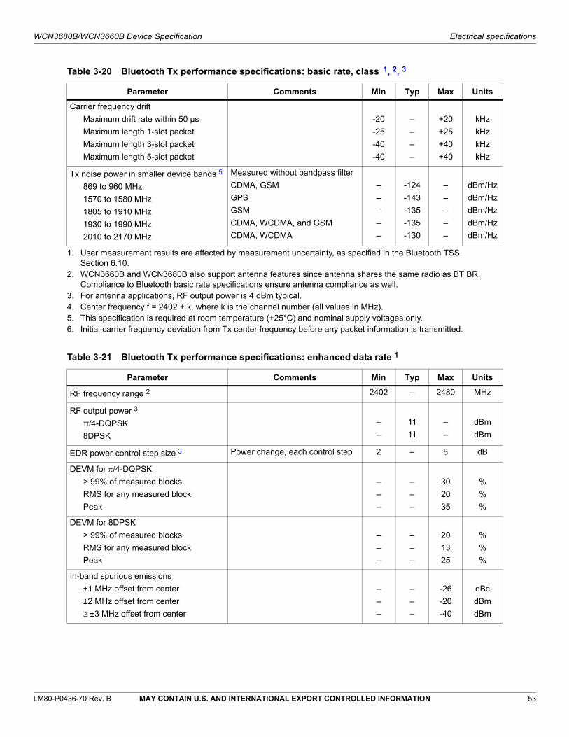
LM80-P0436-70 Rev. B MAY CONTAIN U.S. AND INTERNATIONAL EXPORT CONTROLLED INFORMATION 53
WCN3680B/WCN3660B Device Specification Electrical specifications
Carrier frequency drift
Maximum drift rate within 50 µs
Maximum length 1-slot packet
Maximum length 3-slot packet
Maximum length 5-slot packet
-20
-25
-40
-40
–
–
–
–
+20
+25
+40
+40
kHz
kHz
kHz
kHz
Tx noise power in smaller device bands 5
869 to 960 MHz
1570 to 1580 MHz
1805 to 1910 MHz
1930 to 1990 MHz
2010 to 2170 MHz
Measured without bandpass filter
CDMA, GSM
GPS
GSM
CDMA, WCDMA, and GSM
CDMA, WCDMA
–
–
–
–
–
-124
-143
-135
-135
-130
–
–
–
–
–
dBm/Hz
dBm/Hz
dBm/Hz
dBm/Hz
dBm/Hz
1. User measurement results are affected by measurement uncertainty, as specified in the Bluetooth TSS, Section 6.10.
2. WCN3660B and WCN3680B also support antenna features since antenna shares the same radio as BT BR. Compliance to Bluetooth basic rate specifications ensure antenna compliance as well.
3. For antenna applications, RF output power is 4 dBm typical.4. Center frequency f = 2402 + k, where k is the channel number (all values in MHz).5. This specification is required at room temperature (+25°C) and nominal supply voltages only.6. Initial carrier frequency deviation from Tx center frequency before any packet information is transmitted.
Table 3-21 Bluetooth Tx performance specifications: enhanced data rate 1
Parameter Comments Min Typ Max Units
RF frequency range 2 2402 – 2480 MHz
RF output power 3
π/4-DQPSK
8DPSK
–
–
11
11
–
–
dBm
dBm
EDR power-control step size 3 Power change, each control step 2 – 8 dB
DEVM for /4-DQPSK
> 99% of measured blocks
RMS for any measured block
Peak
–
–
–
–
–
–
30
20
35
%
%
%
DEVM for 8DPSK
> 99% of measured blocks
RMS for any measured block
Peak
–
–
–
–
–
–
20
13
25
%
%
%
In-band spurious emissions
±1 MHz offset from center
±2 MHz offset from center
±3 MHz offset from center
–
–
–
–
–
–
-26
-20
-40
dBc
dBm
dBm
Table 3-20 Bluetooth Tx performance specifications: basic rate, class11, 2, 3
Parameter Comments Min Typ Max Units

LM80-P0436-70 Rev. B MAY CONTAIN U.S. AND INTERNATIONAL EXPORT CONTROLLED INFORMATION 54
WCN3680B/WCN3660B Device Specification Electrical specifications
Frequency errors
Packet error (ωi)Block error (ωo)
Total error (ωi + ωo)
Initial error, all packets
Error for RMS DEVM, all blocks
Total, all blocks
-75
-10
-75
–
–
–
+75
+10
+75
kHz
kHz
kHz
Tx noise power in smaller device bands 4
869 to 960 MHz
1570 to 1580 MHz
1805 to 1910 MHz
1930 to 1990 MHz
2010 to 2170 MHz
Measured without bandpass filter
CDMA, GSM
GPS
GSM, DCS
GSM, PCS, CDMA, WCDMA
WCDMA
–
–
–
–
–
-124
-143
-135
-135
-130
–
–
–
–
–
dBm/Hz
dBm/Hz
dBm/Hz
dBm/Hz
dBm/Hz
1. User measurement results are affected by measurement uncertainty, as specified in the Bluetooth TSS, Section 6.10.
2. Center frequency f = 2402 + k, where k is the channel number (all values in MHz).3. EDR power measured in the GFSK header.4. This specification is required at room temperature (+25°C) and nominal supply voltages only.
Table 3-22 Bluetooth Tx performance specifications: low-energy mode
Parameter Comments Min Typ Max Units
RF frequency range 1
1. Center frequency f = 2402 + k, where k is the channel number (all values in MHz).
2402 – 2480 MHz
Average output power (PAVG) 2
2. Adjustable to any equivalent BR power level.
Maximum output power setting – 4 – dBm
In-band emissions
fTX ± 1 MHz
fTX ± 2 MHz
fTX ± (3 + n) MHz
–
–
–
–
–
–
-26
-20
-30
dBc
dBm
dBm
Modulation characteristics
∆f1avg
∆f2max 185 kHz
∆f1avg/∆f1avg
Recorded over 10 test packets
225
99.9
0.8
–
–
–
275
–
–
kHz
%
–
Carrier frequency offset and drift
fn – fTX, n = 0, 1, 2, 3...k
|f0 – fn|, n = 2, 3, 4...k
|f1 – f0|
|fn – fn-5|, n = 6, 7, 8...k
fTX is the nominal Tx frequency
-150
–
–
–
–
–
–
–
+150
50
20
20
kHz
kHz
kHz
kHz
Table 3-21 Bluetooth Tx performance specifications: enhanced data rate 1 (cont.)
Parameter Comments Min Typ Max Units

LM80-P0436-70 Rev. B MAY CONTAIN U.S. AND INTERNATIONAL EXPORT CONTROLLED INFORMATION 55
WCN3680B/WCN3660B Device Specification Electrical specifications
3.10.2 Bluetooth RF Rx
Bluetooth RF receiver specifications are listed according to three operating modes: the basic rate (Table 3-23), the enhanced data rate (Table 3-24), and low-energy mode (Table 3-25). All typical performance specifications, unless noted otherwise, are based on operation at room temperature (+25°C) using default parameter settings and nominal supply voltages.
Table 3-23 Bluetooth Rx performance specifications: basic rate 1
Parameter Comments Min Typ Max Units
RF frequency range 2 2402 – 2480 MHz
Sensitivity BER ≤ 0.1% – -95 -91 dBm
Maximum usable input 3 BER ≤ 0.1% 0 – – dBm
Carrier-to-interference ratios (C/I) 3
Co-channel
Adjacent channel (±1 MHz)
Second adjacent channel (±2 MHz)
Third adjacent channel (±3 MHz)
BER ≤ 0.1%
–
–
–
–
–
–
–
–
11
0
-30
-40
dB
dB
dB
dB
Intermodulation 3, 4, 5 -39 – – dBm

LM80-P0436-70 Rev. B MAY CONTAIN U.S. AND INTERNATIONAL EXPORT CONTROLLED INFORMATION 56
WCN3680B/WCN3660B Device Specification Electrical specifications
Out-of-band blocking 3, 6
BT 30 to 2000 MHz
2000 to 2400 MHz
2500 to 3000 MHz
3000 to 12750 MHz
Cellular blocking
CDMA2000™ 410 to 420 MHz
450 to 460 MHz
479 to 484 MHz
777 to 792 MHz
806 to 849 MHz
872 to 925 MHz
1710 to 1785 MHz
1850 to 1910 MHz
1920 to 1980 MHz
GSM 450 to 460 MHz
479 to 484 MHz
777 to 792 MHz
824 to 849 MHz
876 to 915 MHz
1710 to 1785 MHz
1850 to 1910 MHz
WCDMA
1710 to 1785 MHz
1850 to 1910 MHz
1920 to 1980 MHz
Measured without bandpass filter
-10
-27
-27
-10
-7
-7
-7
-7
-7
-7
-7
-7
-7
-7
-7
-1
-1
-1
-1
-1
-1
-1
-2
-2
-2
–
–
–
–
–
–
–
–
–
–
–
–
–
–
–
–
–
–
–
–
–
–
–
–
–
–
–
–
–
–
–
–
–
–
–
–
–
–
–
–
–
–
–
–
–
–
–
–
–
–
dBm
dBm
dBm
dBm
dBm
dBm
dBm
dBm
dBm
dBm
dBm
dBm
dBm
dBm
dBm
dBm
dBm
dBm
dBm
dBm
dBm
dBm
dBm
dBm
dBm
1. User measurement results are affected by measurement uncertainty, as specified in the Bluetooth TSS, Section 6.10.
2. Center frequency f = 2402 + k, where k is the channel number (all values in MHz).3. This specification is required at room temperature (+25°C) and normal supply voltages only. 4. Maximum interferer level to maintain 0.1% BER; interference signals at 3 MHz and 6 MHz offsets.5. Intermodulation performance specification is valid with minimum BPF insertion loss of 1.5 dB.6. Continuous power in smaller device bands, -67 dBm desired signal input level. The stated typical values in smaller
device bands are average values measured in accordance with Bluetooth TSS, with less than 24 exceptions.
Table 3-23 Bluetooth Rx performance specifications: basic rate 1 (cont.)
Parameter Comments Min Typ Max Units
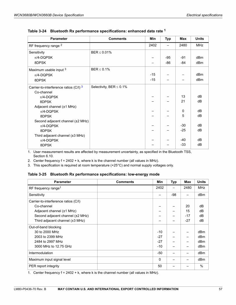
LM80-P0436-70 Rev. B MAY CONTAIN U.S. AND INTERNATIONAL EXPORT CONTROLLED INFORMATION 57
WCN3680B/WCN3660B Device Specification Electrical specifications
Table 3-24 Bluetooth Rx performance specifications: enhanced data rate 1
1. User measurement results are affected by measurement uncertainty, as specified in the Bluetooth TSS, Section 6.10.
Parameter Comments Min Typ Max Units
RF frequency range 2
2. Center frequency f = 2402 + k, where k is the channel number (all values in MHz).
2402 – 2480 MHz
Sensitivity
/4-DQPSK
8DPSK
BER 0.01%
–
–
-95
-86
-91
-84
dBm
dBm
Maximum usable input 3
/4-DQPSK
8DPSK
3. This specification is required at room temperature (+25°C) and normal supply voltages only.
BER 0.1%
-15
-15
–
–
–
–
dBm
dBm
Carrier-to-interference ratios (C/I) 3
Co-channel/4-DQPSK8DPSK
Adjacent channel (±1 MHz)/4-DQPSK8DPSK
Second adjacent channel (±2 MHz)/4-DQPSK8DPSK
Third adjacent channel (±3 MHz)/4-DQPSK8DPSK
Selectivity, BER 0.1%
––
––
––
––
––
––
––
––
1321
05
-30-25
-40-33
dBdB
dBdB
dBdB
dBdB
Table 3-25 Bluetooth Rx performance specifications: low-energy mode
Parameter Comments Min Typ Max Units
RF frequency range1
1. Center frequency f = 2402 + k, where k is the channel number (all values in MHz).
2402 – 2480 MHz
Sensitivity – -98 – dBm
Carrier-to-interference ratios (C/I)Co-channel Adjacent channel (±1 MHz)Second adjacent channel (±2 MHz)Third adjacent channel (±3 MHz)
––––
––––
2015-17-27
dBdBdBdB
Out-of-band blocking30 to 2000 MHz2003 to 2399 MHz2484 to 2997 MHz3000 MHz to 12.75 GHz
-10-27-27-10
––––
––––
dBmdBmdBmdBm
Intermodulation -50 – – dBm
Maximum input signal level 0 – – dBm
PER report integrity 50 – – %
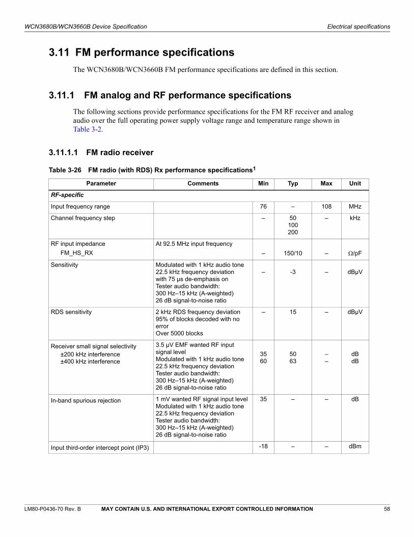
LM80-P0436-70 Rev. B MAY CONTAIN U.S. AND INTERNATIONAL EXPORT CONTROLLED INFORMATION 58
WCN3680B/WCN3660B Device Specification Electrical specifications
3.11 FM performance specifications
The WCN3680B/WCN3660B FM performance specifications are defined in this section.
3.11.1 FM analog and RF performance specifications
The following sections provide performance specifications for the FM RF receiver and analog audio over the full operating power supply voltage range and temperature range shown in Table 3-2.
3.11.1.1 FM radio receiver
Table 3-26 FM radio (with RDS) Rx performance specifications1
Parameter Comments Min Typ Max Unit
RF-specific
Input frequency range 76 – 108 MHz
Channel frequency step – 50100200
– kHz
RF input impedance
FM_HS_RX
At 92.5 MHz input frequency
– 150/10 – /pF
Sensitivity Modulated with 1 kHz audio tone22.5 kHz frequency deviationwith 75 µs de-emphasis onTester audio bandwidth: 300 Hz–15 kHz (A-weighted)26 dB signal-to-noise ratio
– -3 – dBµV
RDS sensitivity 2 kHz RDS frequency deviation95% of blocks decoded with no errorOver 5000 blocks
– 15 – dBµV
Receiver small signal selectivity±200 kHz interference±400 kHz interference
3.5 µV EMF wanted RF input signal levelModulated with 1 kHz audio tone22.5 kHz frequency deviationTester audio bandwidth: 300 Hz–15 kHz (A-weighted)26 dB signal-to-noise ratio
3560
5063
––
dBdB
In-band spurious rejection 1 mV wanted RF signal input levelModulated with 1 kHz audio tone22.5 kHz frequency deviationTester audio bandwidth:300 Hz–15 kHz (A-weighted)26 dB signal-to-noise ratio
35 – – dB
Input third-order intercept point (IP3) -18 – – dBm
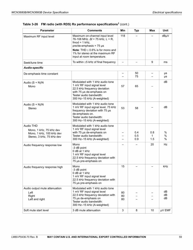
LM80-P0436-70 Rev. B MAY CONTAIN U.S. AND INTERNATIONAL EXPORT CONTROLLED INFORMATION 59
WCN3680B/WCN3660B Device Specification Electrical specifications
Maximum RF input level Maximum on-channel input level 76-108 MHz. ∆f = 75 kHz, L = R, fmod = 1 kHz,pre/de-emphasis = 75 µs
Note: THD 0.6% is for mono and 1% for stereo at the maximum RF input at room temperature.
118 – – dBµV
Seek/tune time To within 5 kHz of final frequency – – 9 ms
Audio-specific
De-emphasis time constant ––
5075
––
µsµs
Audio (S + N)/NMono
Modulated with 1 kHz audio tone1 mV RF input signal level 22.5 kHz frequency deviationwith 75 µs de-emphasis onTester audio bandwidth:300 Hz–15 kHz (A-weighted)
57 65 –
dB
Audio (S + N)/NStereo
Modulated with 1 kHz audio tone1 mV RF input signal level, 75 kHzfrequency deviation with 75 µsde-emphasis on. Tester audio bandwidth:300 Hz–15 kHz (A-weighted)
53 58 – dB
Audio THD
Mono, 1 kHz, 75 kHz devMono, 1 kHz, 100 kHz devStereo, 3 kHz, 75 kHz dev
Modulated with 1 kHz audio tone1 mV RF input signal levelwith 75 µs de-emphasis onTester audio bandwidth: 300 Hz–15 kHz (A-weighted)
–––
0.40.50.9
0.81
1.5
%%%
Audio frequency response low Mono-3 dB point0 dB at 1 kHz1 mV RF input signal level22.5 kHz frequency deviation with 75 µs pre-emphasis on
– – 20 Hz
Audio frequency response high Mono-3 dB point0 dB at 1 kHz1 mV RF input signal level22.5 kHz frequency deviation with 75 µs pre-emphasis on
15 – – kHz
Audio output mute attenuation
LeftRightLeft and right
Modulated with 1 kHz audio tone1 mV RF input signal level22.5 kHz frequency deviation with 75 µs de-emphasis onTester audio bandwidth: 300 Hz–15 kHz (A-weighted)
808080
–––
–––
dBdBdB
Soft mute start level 3 dB mute attenuation 3 8 10 µV EMF
Table 3-26 FM radio (with RDS) Rx performance specifications1 (cont.)
Parameter Comments Min Typ Max Unit
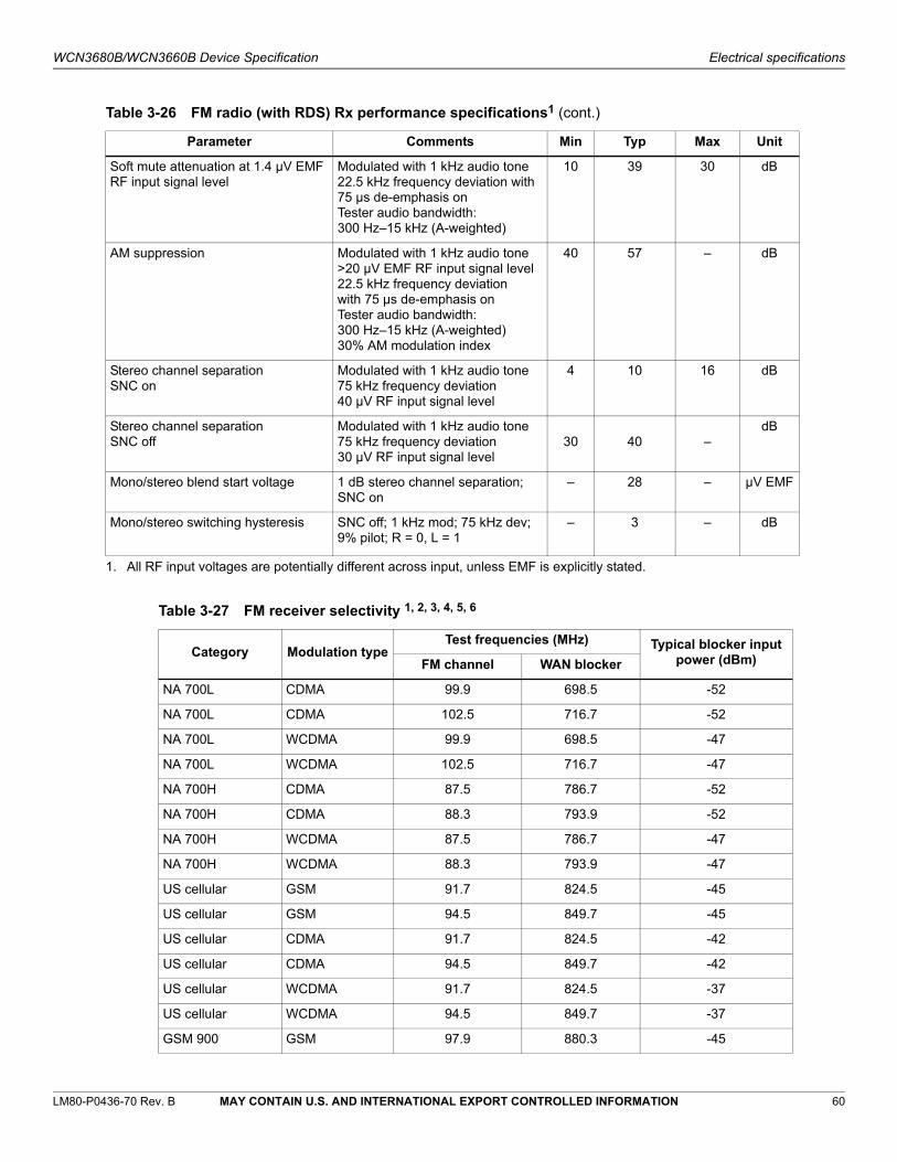
LM80-P0436-70 Rev. B MAY CONTAIN U.S. AND INTERNATIONAL EXPORT CONTROLLED INFORMATION 60
WCN3680B/WCN3660B Device Specification Electrical specifications
Soft mute attenuation at 1.4 µV EMF RF input signal level
Modulated with 1 kHz audio tone22.5 kHz frequency deviation with 75 µs de-emphasis onTester audio bandwidth: 300 Hz–15 kHz (A-weighted)
10 39 30 dB
AM suppression Modulated with 1 kHz audio tone>20 µV EMF RF input signal level22.5 kHz frequency deviationwith 75 µs de-emphasis onTester audio bandwidth: 300 Hz–15 kHz (A-weighted)30% AM modulation index
40 57 – dB
Stereo channel separationSNC on
Modulated with 1 kHz audio tone75 kHz frequency deviation40 µV RF input signal level
4 10 16 dB
Stereo channel separationSNC off
Modulated with 1 kHz audio tone75 kHz frequency deviation30 µV RF input signal level
30 40 –dB
Mono/stereo blend start voltage 1 dB stereo channel separation; SNC on
– 28 – µV EMF
Mono/stereo switching hysteresis SNC off; 1 kHz mod; 75 kHz dev;9% pilot; R = 0, L = 1
– 3 – dB
1. All RF input voltages are potentially different across input, unless EMF is explicitly stated.
Table 3-26 FM radio (with RDS) Rx performance specifications1 (cont.)
Parameter Comments Min Typ Max Unit
Table 3-27 FM receiver selectivity 1, 2, 3, 4, 5, 6
Category Modulation typeTest frequencies (MHz) Typical blocker input
power (dBm)FM channel WAN blocker
NA 700L CDMA 99.9 698.5 -52
NA 700L CDMA 102.5 716.7 -52
NA 700L WCDMA 99.9 698.5 -47
NA 700L WCDMA 102.5 716.7 -47
NA 700H CDMA 87.5 786.7 -52
NA 700H CDMA 88.3 793.9 -52
NA 700H WCDMA 87.5 786.7 -47
NA 700H WCDMA 88.3 793.9 -47
US cellular GSM 91.7 824.5 -45
US cellular GSM 94.5 849.7 -45
US cellular CDMA 91.7 824.5 -42
US cellular CDMA 94.5 849.7 -42
US cellular WCDMA 91.7 824.5 -37
US cellular WCDMA 94.5 849.7 -37
GSM 900 GSM 97.9 880.3 -45

LM80-P0436-70 Rev. B MAY CONTAIN U.S. AND INTERNATIONAL EXPORT CONTROLLED INFORMATION 61
WCN3680B/WCN3660B Device Specification Electrical specifications
GSM 900 GSM 101.7 914.5 -45
CDMA 900 CDMA 97.9 880.3 -42
CDMA 900 CDMA 101.7 914.5 -42
WCDMA 900 WCDMA 97.9 880.3 -37
WCDMA 900 WCDMA 101.7 914.5 -37
UMTS 1500 WCDMA 84.1 1428.1 -37
UMTS 1500 WCDMA 85.5 1451.9 -37
GSM 1800 GSM 100.7 1710.3 -45
GSM 1800 GSM 105.1 1785.1 -45
PCS GSM 97.5 1850.5 -45
PCS GSM 100.7 1911.3 -45
PCS CDMA 97.5 1850.5 -42
PCS CDMA 100.7 1911.3 -42
PCS WCDMA 97.5 1850.5 -37
PCS WCDMA 100.7 1911.3 -37
IMT CDMA 101.3 1922.7 -42
IMT CDMA 104.3 1979.7 -42
IMT WCDMA 101.3 1922.7 -37
IMT WCDMA 104.3 1979.7 -37
BT/WLAN BT 104.5 2401.1 -43
BT/WLAN BT 107.9 2479.3 -43
UMTS 2600 WCDMA 100.1 2500.1 -41
UMTS 2600 WCDMA 102.9 2570.1 -41
1. All levels are at the chip input.2. Wanted signal at 5 dBV (-102 dBm 50 or +10.8 dBV EMF) input; fmod = 1 kHz, f = 22.5 kHz
SINAD = 26 dB, BAF = 300 Hz to 15 kHz (A-weighted) de-emphasis = 50 s.3. CDMA blocker is modulated reverse link. 1.2288 Mb/s chip rate.4. WCDMA blocker is modulated reverse link. 3.84 Mb/s chip rate.5. GSM blocker is modulated; MSK modulation; Gaussian filter BT = 0.3; fs = 270.8333 ks/s; and bursting
1/8 timeslots.6. BT blocker is modulated with mod index = 0.315; bursting with DH1 packets.
Table 3-27 FM receiver selectivity 1, 2, 3, 4, 5, 6 (cont.)
Category Modulation typeTest frequencies (MHz) Typical blocker input
power (dBm)FM channel WAN blocker
LM80-P0436-70 Rev. B MAY CONTAIN U.S. AND INTERNATIONAL EXPORT CONTROLLED INFORMATION 62
WCN3680B/WCN3660B Device Specification Electrical specifications
3.11.2 FM RDS interrupt
At reset, the RDS interrupt signal is disabled. After reset, the host can enable the interrupt and set the NVM parameters associated with the interface. The software supports the following NVM parameters for configuring the interrupt behavior:
Inactive mode: tri-state or output
Internal pull (if inactive mode is set to tri-state): up, down, or no-pull
The FM RDS interrupt uses a digital I/O pad that receives power from the VDD_IO_1P8 supply. Its I/O performance specifications meet the requirements stated in Section 3.5.
LM80-P0436-70 Rev. B MAY CONTAIN U.S. AND INTERNATIONAL EXPORT CONTROLLED INFORMATION 63
4 Mechanical information
Mechanical information for the WCN3680B/WCN3660B IC is presented in this chapter, including physical dimensions, visible markings, ordering information, moisture sensitivity level, and thermal characteristics.
4.1 Device physical dimensions
The WCN3680B/WCN3660B IC is available in the 79B WLNSP that includes extra ground pads for improved grounding, mechanical strength, and thermal continuity. The 79B WLNSP package has a 3.805 × 3.82 mm body with a maximum height of 0.63 mm. Pad 1 is located by an indicator mark on the top of the package. The 79B WLNSP outline drawing is shown in Figure 4-1.

WCN3680B/WCN3660B Device Specification Mechanical information
LM80-P0436-70 Rev. B MAY CONTAIN U.S. AND INTERNATIONAL EXPORT CONTROLLED INFORMATION 64
Figure 4-1 79B WLNSP outline drawing
PAGE 52
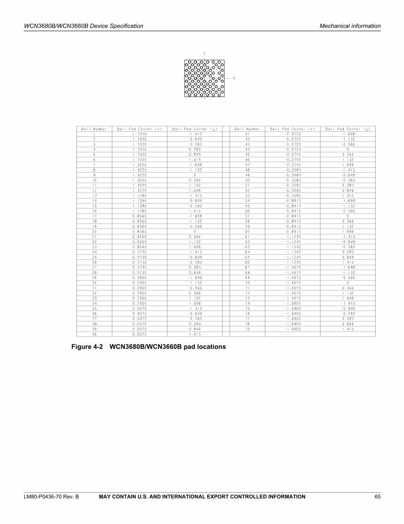
LM80-P0436-70 Rev. B MAY CONTAIN U.S. AND INTERNATIONAL EXPORT CONTROLLED INFORMATION 65
WCN3680B/WCN3660B Device Specification Mechanical information
Figure 4-2 WCN3680B/WCN3660B pad locations

LM80-P0436-70 Rev. B MAY CONTAIN U.S. AND INTERNATIONAL EXPORT CONTROLLED INFORMATION 66
WCN3680B/WCN3660B Device Specification Mechanical information
4.2 Device marking
Section 4.2.1 provides the device marking information for WCN3680B; Section 4.2.2 provides the device marking information for WCN3660B.
4.2.1 WCN3680B
Figure 4-3 WCN3680B part marking (top view – not to scale)
Table 4-1 WCN3680B part marking line descriptions
Line Marking Description
1 WCN3680B Qualcomm product name
2 PBB P = configuration code
BB = feature code
3 XXXXXXXXX XXXXXXXXX = wafer lot number
4 FAYWWRR F = Source of supply code for wafer fab locations
When F = A: Fabrication = TSMC
A = Source of supply code for assembly location
When A = A: Assembly = TSMC, BP2B, Taiwan
When A = B: Assembly = Amkor, ATT3, Taiwan
Y = Single-digit year
WW = Two-digit work week of current year (based on calendar year)
RR = Product revision
RR = 05, Engineering sample 1 (ES) and final commercial sample (CS)
5 ## ## = two-digit wafer number
1 identifier
Line 1Line 2Line 3
WCN3680B
XXXXXXXXXFAYWWRR
PBB
# #Line 4Line 5

LM80-P0436-70 Rev. B MAY CONTAIN U.S. AND INTERNATIONAL EXPORT CONTROLLED INFORMATION 67
WCN3680B/WCN3660B Device Specification Mechanical information
4.2.2 WCN3660B
Figure 4-4 WCN3660B part marking (top view – not to scale)
Table 4-2 WCN3660B part marking line descriptions
Line Marking Description
1 WCN3660B Qualcomm product name
2 PBB P = configuration code
BB = feature code
3 XXXXXXXXX XXXXXXXXX = wafer lot number
4 FAYWWRR F = Source of supply code for wafer fab locations
When F = A: Fabrication = TSMC
A = Source of supply code for assembly location
When A = A: Assembly = TSMC, BP2B, Taiwan
When A = B: Assembly = Amkor, ATT3, Taiwan
Y = Single-digit year
WW = Two-digit work week of current year (based on calendar year)
RR = product revision
RR = 05, Engineering sample 1 (ES) and final commercial sample (CS)
5 ## ## = two-digit wafer number
1 identifier
Line 1Line 2Line 3
WCN3660B
XXXXXXXXXFAYWWRR
PBB
# #Line 4Line 5

LM80-P0436-70 Rev. B MAY CONTAIN U.S. AND INTERNATIONAL EXPORT CONTROLLED INFORMATION 68
WCN3680B/WCN3660B Device Specification Mechanical information
4.3 Device ordering information
This device can be ordered using the identification code shown in Figure 4-5.
Figure 4-5 Device identification code
An example can be as follows: WCN-3680-0-79WLNSP-TR-00-0.
4.4 Device moisture-sensitivity level
During device qualification, Qualcomm follows the latest revision IPC/JEDEC J-STD-020 standard to determine the IC’s moisture-sensitivity level (MSL). See Chapter 7 for more information.
To ensure proper SMT assembly, procedures must follow the MSL and maximum reflow temperature specified on the shipping bag labels or bar code labels accompanying all WCN3680B/WCN3660B IC shipments.
Additional MSL information is included in:
Section 5.2 – Storage
Section 5.3 – Handling
Section 7.1 – Reliability qualifications summary
DDCCCCCBBB RRPAAA-AAAA
RR: Product revision(ex. “00” = engineering sample)
AAA-AAAAN: Product name(ex: WCN-3680)
P: Configuration code (ex. 0)
BBB: Number of pins (ex. 79)
DD: Packing information (ex. "TR"= tape and reel;
“SR” = short reel)
S
CCCCC: Package type (ex. WLNSP)
S: Source code (ex. 0)

LM80-P0436-70 Rev. B MAY CONTAIN U.S. AND INTERNATIONAL EXPORT CONTROLLED INFORMATION 69
WCN3680B/WCN3660B Device Specification Mechanical information
4.5 Thermal characteristics
The WCN3680B/WCN3660B device in its 79B WLNSP package has typical thermal resistances as listed in Table 4-3.
Table 4-3 Device thermal resistance
Parameter Comments Typ Unit
JA Thermal resistance, J-to-A Junction-to-ambient (still air) 1
1. Junction-to-ambient thermal resistance (JA) is calculated based on the total package power dissipation (200 mW); ambient temperature is 85°C.
49.0 °C/W

LM80-P0436-70 Rev. B MAY CONTAIN U.S. AND INTERNATIONAL EXPORT CONTROLLED INFORMATION 70
5 Carrier, storage, and handling information
Information about shipping, storing, and handling the WCN3680B/WCN3660B IC is presented in this chapter.
5.1 Shipping
5.1.1 Tape and reel information
The single-feed tape carrier for the WCN3680B/WCN3660B device is illustrated in Figure 5-1; this figure also shows the proper part orientation. The tape width is 12 mm, and the parts are placed on the tape with a 8 mm pitch. The reels are 330 mm (13 inch) in diameter, with 178 mm (7 inch) hubs. Each reel can contain up to 5000 devices.
Figure 5-1 Carrier tape drawing with part orientation
WCN3680B
Pin #1 faces feed holes
Taping direction
Tape
wid
th
Pocket pitch
WCN3680BWCN3680B
Pin #1
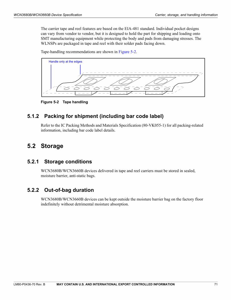
LM80-P0436-70 Rev. B MAY CONTAIN U.S. AND INTERNATIONAL EXPORT CONTROLLED INFORMATION 71
WCN3680B/WCN3660B Device Specification Carrier, storage, and handling information
The carrier tape and reel features are based on the EIA-481 standard. Individual pocket designs can vary from vendor to vendor, but it is designed to hold the part for shipping and loading onto SMT manufacturing equipment while protecting the body and pads from damaging stresses. The WLNSPs are packaged in tape and reel with their solder pads facing down.
Tape-handling recommendations are shown in Figure 5-2.
Figure 5-2 Tape handling
5.1.2 Packing for shipment (including bar code label)
Refer to the IC Packing Methods and Materials Specification (80-VK055-1) for all packing-related information, including bar code label details.
5.2 Storage
5.2.1 Storage conditions
WCN3680B/WCN3660B devices delivered in tape and reel carriers must be stored in sealed, moisture barrier, anti-static bags.
5.2.2 Out-of-bag duration
WCN3680B/WCN3660B devices can be kept outside the moisture barrier bag on the factory floor indefinitely without detrimental moisture absorption.
Handle only at the edges
LM80-P0436-70 Rev. B MAY CONTAIN U.S. AND INTERNATIONAL EXPORT CONTROLLED INFORMATION 72
WCN3680B/WCN3660B Device Specification Carrier, storage, and handling information
5.3 Handling
Unlike traditional IC devices, the silicon in the WCN devices is not protected by an over-mold and there is no substrate; hence, these devices are fragile.
Tape handling is described in Section 5.1.1. Other handling guidelines are presented below.
NOTE To eliminate damage to the silicon die due to improper handling, the following recommendations must be followed:
• Do not use tweezers, as they can cause damage to the silicon die. Use a vacuum tip to handle the device.
• Carefully select a pickup tool to avoid any damage during the SMT process.
• Do not make contact with the device when reworking or tuning components that are in close proximity to the device.
5.3.1 Baking
Wafer level packages, including this device, must not be baked.
5.3.2 Electrostatic discharge
Electrostatic discharge (ESD) occurs naturally in laboratory and factory environments. An established high-voltage potential is always at risk of discharging to a lower potential. If this discharge path is through a semiconductor device, it will result in destructive damage.
ESD countermeasures and handling methods must be developed and used to control the factory environment at each manufacturing site.
These products must be handled according to the ESD Association standard: ANSI/ESD S20.20-1999, Protection of Electrical and Electronic Parts, Assemblies, and Equipment.
Refer to Section 7.1 for the WCN3680B/WCN3660B device ESD ratings.

LM80-P0436-70 Rev. B MAY CONTAIN U.S. AND INTERNATIONAL EXPORT CONTROLLED INFORMATION 73
6 PCB mounting guidelines
Guidelines for mounting the WCN3680B/WCN3660B device onto a PCB are presented in this chapter, including land pad and stencil design details, surface mount technology (SMT) process characterization, and SMT process verification.
NOTE Mounting suggestions presented in this chapter are provided for convenience only.
The WCN3680B device is Pb-free internally and externally; it is also BrCl-free, RoHS-compliant, and e1(SAC). Its solder pads use the SAC405 composition.
NOTE The lead-free (or Pb-free) semiconductor products are defined as having a maximum lead concentration of 1000 ppm (0.1% by weight) in raw (homogeneous) materials and end products.
6.1 Land pad and stencil design
The land pattern recommendations are based on the internal characterizations using Pb-free solder pastes on an eight-layer test PCB and a 100-micron thick stencil. The PCB land pattern for the 79B WLNSP package is the same whether SnPb or Pb-free solder is used.
6.2 SMT development and characterization
The information presented in this section describes the board-level characterization process parameters. It is included to assist customers when starting their SMT process development; it is not intended to be a specification for customer SMT processes.
NOTE It is recommended for the customers to follow their solder paste vendor recommendations for the screen-printing process parameters and reflow profile conditions.
The characterization tests optimize the SMT process for the best board-level reliability. This is done by performing physical tests on evaluation boards, which include:
Bend cycle
Drop shock
Temperature cycling

LM80-P0436-70 Rev. B MAY CONTAIN U.S. AND INTERNATIONAL EXPORT CONTROLLED INFORMATION 74
WCN3680B/WCN3660B Device Specification PCB mounting guidelines
Characterizing the land patterns according to each customer's processes, materials, equipment, stencil design, and reflow profile prior to PCB production is recommended. Review the land pattern and stencil pattern design recommendations in Section 6.1 as a guide for characterization.
Any particular underfill products are not endorsed.
Optimizing the solder-stencil pattern design and print process is critical to ensure print uniformity, decrease voiding, and increase board-level reliability.
Reflow profile conditions used for SnPb and lead-free systems are given in Table 6-1.
6.3 SMT peak package-body temperature
The following limits during the SMT board-level solder attach process are recommended:
SMT peak package-body temperature of 250 ºC, the temperature that must not be exceeded as measured on the package-body’s top surface.
Maximum duration of 30 sec. at this temperature.
Although the solder-paste manufacturer’s recommendations for optimum temperature and duration for solder reflow must be followed, the recommended limits must not be exceeded.
6.4 SMT process verification
The verification of the SMT process prior to high-volume PCB fabrication is recommended, including:
Electrical continuity
X-ray inspection of the package installation for proper alignment, solder voids, solder pads, and solder bridging
Visual inspection
Cross-section inspection of solder joints to confirm registration, fillet shape, and print volume (insufficient, acceptable, or excessive)
Table 6-1 SMT reflow profile conditions (for reference only)
Profile stage DescriptionLead-free (high-temperature)
condition limits
Preheat Initial ramp 3°C/sec max
Soak Dry out and flux activation 150 to 190°C
60 to 120 sec
Reflow Time above solder-paste melting point 40 to 75 sec
Peak temperature 250°C
Cool down Cool rate – ramp to ambient 6°C/sec max

LM80-P0436-70 Rev. B MAY CONTAIN U.S. AND INTERNATIONAL EXPORT CONTROLLED INFORMATION 75
7 Part reliability
7.1 Reliability qualification summary
Table 7-1 WCN3680B/WCN3660B reliability qualification report for a device from TSMC and WLNSP package from TSMC and Amkor
Tests, standards, and conditionsSample
number of lotsResults(TSMC)
Results(Amkor)
Average failure rate (AFR) in FIT () failures per billion device hours
Functional HTOL: JESD22-A108
535
3 lots = 15 FIT N/A
Mean time to failure (MTTF) t = 1/ (million hours)
535
3 lots
67 N/A
ESD – human body model (HBM) rating
JESD22-A114-B
3 Pass ± 2000 V,
all pads
N/A
ESD – charged device model (CDM) rating
JESD22-C101-D
3 Pass ± 500 V,
all pads
N/A
Latch-up (overcurrent test): EIA/JESD78
Trigger current: ±100 mA; temperature: 85C6 Pass N/A
Latch-up (Vsupply overvoltage): EIA/JESD78
Trigger voltage: 1.5 × V; temperature: 85C6 Pass N/A
Moisture resistance test (MRT): MSL 1; J-STD-020
3 X reflow cycles at 255 +/-5 C
462
3 lots
Pass Pass
Temperature cycle: JESD22-A104
Temperature: -55C to +125C; number of cycles: 1000
Minimum soak time at min/max temperature: five minutes
Cycle rate: two cycles per hour (CPH)
Preconditioning: JESD22-A113
MSL: 1 reflow temperature: 255C+5/-0C
231
3 lots
Pass Pass
Unbiased highly accelerated stress test (UHAST)
JESD22-A118
Preconditioning: JESD22-A113
MSL: 1 reflow temperature: 255 +5/-0C
231
3 lots
Pass Pass
High temperature storage life: JESD22-A103
Temperature 150C, 1000 hours
78
3 lots
Pass Pass
LM80-P0436-70 Rev. B MAY CONTAIN U.S. AND INTERNATIONAL EXPORT CONTROLLED INFORMATION 76
WCN3680B/WCN3660B Device Specification Part reliability
7.2 Qualification sample description
WCN3680B device characteristics
Device name: WCN3680B
Package type: 79B WLNSP
Package body size: 3.805 mm × 3.82 mm × 0.63 mm
BGA pad count: 79
BGA pad composition: SAC405
Processes: 65 nm RF CMOS
Fab site: See note.
Assembly sites: See note.
Solder pad pitch: 0.4 mm minimum
WCN3660B device characteristics
Device name: WCN3660B
Package type: 79B WLNSP
Package body size: 3.805 mm × 3.82 mm × 0.63 mm
BGA pad count: 79
BGA pad composition: SAC405
Processes: 65 nm RF CMOS
Fab site: See the note.
Assembly sites: See the note.
Solder pad pitch: 0.4 mm minimum
NOTE Refer to the WCN3680B/WCB3660B Device Revision Guide (LM80-P0436-71) for fab and assembly sites.
Physical dimensions: JESD22-B100-A
Package outline drawing: NT90-N2742-1
15 Pass Pass
Solder pad shear: JESD22-B117
After 10x reflow cycles 260C -5/+0C40 pads
(four pads per sample × 10 samples)
Pass
(all pads sheared in ductile mode)
Pass
(all pads sheared in ductile mode)
Table 7-1 WCN3680B/WCN3660B reliability qualification report for a device from TSMC and WLNSP package from TSMC and Amkor (cont.)
Tests, standards, and conditionsSample
number of lotsResults(TSMC)
Results(Amkor)

LM80-P0436-70 Rev. B MAY CONTAIN U.S. AND INTERNATIONAL EXPORT CONTROLLED INFORMATION 77
EXHIBIT 1
PLEASE READ THIS LICENSE AGREEMENT (“AGREEMENT”) CAREFULLY. THIS AGREEMENT IS A BINDING LEGAL AGREEMENT ENTERED INTO BY AND BETWEEN YOU (OR IF YOU ARE ENTERING INTO THIS AGREEMENT ON BEHALF OF AN ENTITY, THEN THE ENTITY THAT YOU REPRESENT) AND QUALCOMM TECHNOLOGIES, INC. (“QTI” “WE” “OUR” OR “US”). THIS IS THE AGREEMENT THAT APPLIES TO YOUR USE OF THE DESIGNATED AND/OR ATTACHED DOCUMENTATION AND ANY UPDATES OR IMPROVEMENTS THEREOF (COLLECTIVELY, “MATERIALS”). BY USING OR COMPLETING THE INSTALLATION OF THE MATERIALS, YOU ARE ACCEPTING THIS AGREEMENT AND YOU AGREE TO BE BOUND BY ITS TERMS AND CONDITIONS. IF YOU DO NOT AGREE TO THESE TERMS, QTI IS UNWILLING TO AND DOES NOT LICENSE THE MATERIALS TO YOU. IF YOU DO NOT AGREE TO THESE TERMS YOU MUST DISCONTINUE AND YOU MAY NOT USE THE MATERIALS OR RETAIN ANY COPIES OF THE MATERIALS. ANY USE OR POSSESSION OF THE MATERIALS BY YOU IS SUBJECT TO THE TERMS AND CONDITIONS SET FORTH IN THIS AGREEMENT.
1.1 License. Subject to the terms and conditions of this Agreement, including, without limitation, the restrictions, conditions, limitations and exclusions set forth in this Agreement, Qualcomm Technologies, Inc. (“QTI”) hereby grants to you a nonexclusive, limited license under QTI’s copyrights to use the attached Materials; and to reproduce and redistribute a reasonable number of copies of the Materials. You may not use Qualcomm Technologies or its affiliates or subsidiaries name, logo or trademarks; and copyright, trademark, patent and any other notices that appear on the Materials may not be removed or obscured. QTI shall be free to use suggestions, feedback or other information received from You, without obligation of any kind to You. QTI may immediately terminate this Agreement upon your breach. Upon termination of this Agreement, Sections 1.2-4 shall survive.
1.2 Indemnification. You agree to indemnify and hold harmless QTI and its officers, directors, employees and successors and assigns against any and all third party claims, demands, causes of action, losses, liabilities, damages, costs and expenses, incurred by QTI (including but not limited to costs of defense, investigation and reasonable attorney’s fees) arising out of, resulting from or related to: (i) any breach of this Agreement by You; and (ii) your acts, omissions, products and services. If requested by QTI, You agree to defend QTI in connection with any third party claims, demands, or causes of action resulting from, arising out of or in connection with any of the foregoing.
1.3 Ownership. QTI (or its licensors) shall retain title and all ownership rights in and to the Materials and all copies thereof, and nothing herein shall be deemed to grant any right to You under any of QTI's or its affiliates’ patents. You shall not subject the Materials to any third party license terms (e.g., open source license terms). You shall not use the Materials for the purpose of identifying or providing evidence to support any potential patent infringement claim against QTI, its affiliates, or any of QTI’s or QTI’s affiliates’ suppliers and/or direct or indirect customers. QTI hereby reserves all rights not expressly granted herein.
1.4 WARRANTY DISCLAIMER. YOU EXPRESSLY ACKNOWLEDGE AND AGREE THAT THE USE OF THE MATERIALS IS AT YOUR SOLE RISK. THE MATERIALS AND TECHNICAL SUPPORT, IF ANY, ARE PROVIDED "AS IS" AND WITHOUT WARRANTY OF ANY KIND, WHETHER EXPRESS OR IMPLIED. QTI ITS LICENSORS AND AFFILIATES MAKE NO WARRANTIES, EXPRESS OR IMPLIED, WITH RESPECT TO THE MATERIALS OR ANY OTHER INFORMATION OR DOCUMENTATION PROVIDED UNDER THIS AGREEMENT, INCLUDING BUT NOT LIMITED TO ANY WARRANTY OF MERCHANTABILITY OR FITNESS FOR A PARTICULAR PURPOSE OR AGAINST INFRINGEMENT, OR ANY EXPRESS OR IMPLIED WARRANTY ARISING OUT OF TRADE USAGE OR OUT OF A COURSE OF DEALING OR COURSE OF PERFORMANCE. NOTHING CONTAINED IN THIS AGREEMENT SHALL BE CONSTRUED AS (I) A WARRANTY OR REPRESENTATION BY QTI, ITS LICENSORS OR AFFILIATES AS TO THE VALIDITY OR SCOPE OF ANY PATENT, COPYRIGHT OR OTHER INTELLECTUAL PROPERTY RIGHT OR (II) A WARRANTY OR REPRESENTATION BY QTI THAT ANY MANUFACTURE OR USE WILL BE FREE FROM INFRINGEMENT OF PATENTS, COPYRIGHTS OR OTHER INTELLECTUAL PROPERTY RIGHTS OF OTHERS, AND IT SHALL BE THE SOLE RESPONSIBILITY OF YOU TO MAKE SUCH DETERMINATION AS IS NECESSARY WITH RESPECT TO THE ACQUISITION OF LICENSES UNDER PATENTS AND OTHER INTELLECTUAL PROPERTY OF THIRD PARTIES.
1.5 LIMITATION OF LIABILITY. IN NO EVENT SHALL QTI, QTI’S AFFILIATES OR ITS LICENSORS BE LIABLE TO YOU FOR ANY INCIDENTAL, CONSEQUENTIAL OR SPECIAL DAMAGES, INCLUDING BUT NOT LIMITED TO ANY LOST PROFITS, LOST SAVINGS, OR OTHER INCIDENTAL DAMAGES, ARISING OUT OF THE USE OR INABILITY TO USE, OR THE DELIVERY OR FAILURE TO DELIVER, ANY OF THE MATERIALS, OR ANY BREACH OF ANY OBLIGATION UNDER THIS AGREEMENT, EVEN IF QTI HAS BEEN ADVISED OF THE POSSIBILITY OF SUCH DAMAGES. THE FOREGOING LIMITATION OF LIABILITY SHALL REMAIN IN FULL FORCE AND EFFECT REGARDLESS OF WHETHER YOUR REMEDIES HEREUNDER ARE DETERMINED TO HAVE FAILED OF THEIR ESSENTIAL PURPOSE. THE ENTIRE LIABILITY OF QTI, QTI’s AFFILIATES AND ITS LICENSORS, AND THE SOLE AND EXCLUSIVE REMEDY OF YOU, FOR ANY CLAIM OR CAUSE OF ACTION ARISING HEREUNDER (WHETHER IN CONTRACT, TORT, OR OTHERWISE) SHALL NOT EXCEED US$10.2. COMPLIANCE WITH LAWS; APPLICABLE LAW. You agree to comply with all applicable local, international and national laws and regulations and with U.S. Export Administration Regulations, as they apply to the subject matter of this Agreement. This Agreement is governed by the laws of the State of California, excluding California’s choice of law rules. 3. CONTRACTING PARTIES. If the Materials are downloaded on any computer owned by a corporation or other legal entity, then this Agreement is formed by and between QTI and such entity. The individual accepting the terms of this Agreement represents and warrants to QTI that they have the authority to bind such entity to the terms and conditions of this Agreement.4.MISCELLANEOUS PROVISIONS. This Agreement, together with all exhibits attached hereto, which are incorporated herein by this refer-ence, constitutes the entire agreement between QTI and You and supersedes all prior negotiations, representations and agreements between the parties with respect to the subject matter hereof. No addition or modification of this Agreement shall be effective unless made in writing and signed by the respective representatives of QTI and You. The restrictions, limitations, exclusions and conditions set forth in this Agreement shall apply even if QTI or any of its affiliates becomes aware of or fails to act in a manner to address any violation or failure to comply therewith. You hereby acknowledge and agree that the restrictions, limitations, conditions and exclusions imposed in this Agreement on the rights granted in this Agreement are not a derogation of the benefits of such rights. You further acknowledges that, in the absence of such restrictions, limitations, con-ditions and exclusions, QTI would not have entered into this Agreement with You. Each party shall be responsible for and shall bear its own expenses in connection with this Agreement. If any of the provisions of this Agreement are determined to be invalid, illegal, or otherwise unen-forceable, the remaining provisions shall remain in full force and effect. This Agreement is entered into solely in the English language, and if for any reason any other language version is prepared by any party, it shall be solely for convenience and the English version shall govern and control all aspects. If You are located in the province of Quebec, Canada, the following applies: The Parties hereby confirm they have requested this Agreement and all related documents be prepared in English.