waveguide-type optical circuits for recognition of optical
TRANSCRIPT

Japanese Journal of Applied Physics REGULAR PAPER
Waveguide-type optical circuits for recognition of optical8PSK-coded labels
Munkhbayar Adiya1, Nyam-Erdene Odbayar1∗, Hiroki Kishikawa1†, Nobuo Goto1,
Ganbold Shagdar2
1Department of Optical Science, Tokushima University, 2-1 Minamijosanjima-cho, Tokushima, 770-8506
Japan2Mongolian University of Science and Technology, School of Information and Communication Technology,
Ulaanbaatar-13343, Mongolia
This paper discusses optical label recognition for photonic label routing. The label recognition is one of
the key function in photonic label routing related functions including optical label extraction, recognition
of the label and label rewriting. In previous study, we have proposed a basic waveguide-type circuit for
recognition of optical label encoded in quadri-phase-shift-keying (QPSK) format, which consists of 3-dB
directional coupler, two Y-branches and an asymmetric X junction coupler. In order to increase the number
of labels represented by the same symbol number, we propose 8PSK recognition circuits based on the
QPSK recognition circuit. The input-output relation of the proposed circuits is theoretically discussed and
the noise tolerance is also investigated. From the theoretical analysis, the proposed optical-waveguide
circuits recognize the 8PSK labels by detecting the position of the output port having either the maximum
or minimum intensity. The bit-error performance of the proposed circuits is clarified by computer simulation.
It is found that the minimum-output detection scheme for one-symbol 8PSK label is superior from the
viewpoint of noise tolerance. The proposed method also addresses the scalability of two-symbol 8PSK
coded labels. The maximum-output detection scheme demonstrates improved scalability performance.
1. Introduction
Technological development in telecommunication systems to meet the growing demand of
communication traffic requires faster speed, larger capacity and broader-band transmission.
In conventional optical network systems, electrical signal processing is applied to the routing
node together with optical-to-electrical and electrical-to-optical conversion. This conversion
takes time for processing and requires power consumption which makes transmission sys-
tem more complex. The optical signal processing without conversion to electrical signals is
expected to be applied to routing nodes to overcome those disadvantages.1)
∗M. Adiya and N. Odbayar equally contributed to this work.†E-mail: [email protected]
1/18
The final authenticated version is available online at:https://doi.org/10.7567/1347-4065/ab1b65
Jpn. J. Appl. Phys. REGULAR PAPER
Various optical signal processing functions performed in routers include optical label ex-
traction, recognition of the label, optical switching and buffering, and label rewriting. We
focus on photonic label recognition methods among these signal processing functions. As
one of the nature of light, phase of coherent light has been effectively used in various opti-
cal systems, where the passive interference behavior between multiple signals is easily used.
Using this feature, label recognition techniques have been investigated for photonic routers
based on optical code correlation.2–9) However, most of the proposed systems could not rec-
ognize all the binary codes because only the type of codes that provide enough discrimination
between auto-correlation and cross-correlation were recognized.4,10–12)A self-routing archi-
tecture was proposed for the label recognition system in which optical active elements have
chosen to identify label information,13) where multiple label recognition for on-off keying
(OOK) codes was achieved. Other types of optical label recognition techniques include an
optical method based on optical serial-to-parallel conversion and spin-polarized all-optical
switch,14) a method using optical digital-to-analog conversion,15) and a CMOS-based low-
power-consumption label processor.16) On the other hand, an all-optical passive label recog-
nition system for all the binary codes in binary phase-shift-keying (BPSK) format was pro-
posed.17) This passive processing scheme provides faster and power efficient processing.18)
Even though, self-routing architecture for label recognition is one of the promising methods
in label decoding system, the number of data streams in transmission systems is enormous,
which requires a large number of routing labels in the networks. The number of represented
labels increases by employing multiple phases such as quadri-phase-shift keying (QPSK) and
quadrature amplitude modulation (QAM) coded labels.19–22)
The QAM modulated pulses have multiple amplitudes, which results in efficient band-
width and high bit rate for transmission. Although the distance between each of the QAM
codes in the signal constellation may be larger compared with a single amplitude codes such
as multiple PSK codes, optical recognition scheme for suchM-ary PSK labels is much sim-
pler. Therefore, we propose optical recognition circuits for 8PSK coded labels. The proposed
circuit is based on the optical QPSK recognition circuit (QPRC)23) which consists of an asym-
metric X-junction coupler, Y-branches and a 3-dB directional coupler. We have proposed two
recognition schemes, that are recognition from maximum output port or from minimum out-
put port. The recognition characteristics for one-symbol labels by maximum-output scheme
was reported.24) For minimum-output scheme, we reported for one- and two-symbol labels.25)
In this paper, we compare these two schemes for one- and two-symbol labels from the view
point of noise tolerance. The electrical power consumption of the proposed circuit is consid-
2/18

Jpn. J. Appl. Phys. REGULAR PAPER
Q
I
Fig. 1. Constellation of 8PSK coded signals.
ered to be low because of the passive integrated-optic devices and thresholders. The recogni-
tion is performed during optical wave propagation through the proposed passive devices and
thresholders. Therefore, the processing speed is expected to be fast.
The proposed waveguide-type 8PSK recognition circuit employs two decision schemes,
i.e., recognition from the maximum output port or from the minimum output port. First,
the input-output relation of the recognition circuit is theoretically analyzed. Then, the bit-
error-rate (BER) characteristics against optical signal-to-noise ratio (OSNR) are evaluated by
numerical simulations using OptiSystem software (Optiwave Systems Inc.) in order to clarify
the label recognition performance since noise tolerance is considered as one of the important
factors in the telecommunication system. For the purpose of comparison, we also build a
back-to-back (B2B) model which uses a digital coherent receiver to recognize 8PSK codes.
In the optical label network system, a large number of routing labels are required. It is
reported that thousands to tens of thousands of labels are required.4) Thus, we propose scaled
two-symbol-length 8PSK label recognition circuits for the two recognition schemes. Similar
scaled circuits can be configured for more than three-symbol-length labels. We evaluate and
compare the BER characteristics between the two recognition schemes.
This paper consists of 4 sections. In Section 2, we describe the proposed recognition
circuits and their theoretical analysis. The noise tolerance of the recognition performance is
numerically simulated in Section 3. Finally, the conclusions are presented in Section 4.
2. 8PSK-Coded Label Recognition Circuit
The constellation diagram of 8PSK codes is illustrated in Fig. 1. The types of PSK include
BPSK, QPSK, andM-ary PSK (8PSK, 16PSK,· · · ). In the 8PSK codes, the carrier phase is
shifted by 8 times and each phase represents 3 bits information.
An example of the optical processing for label recognition is schematically illustrated
in Fig. 2. We assume that an extracted optical label from an incident packet to the router
3/18

Jpn. J. Appl. Phys. REGULAR PAPER
Fig. 2. Optical processing with a label recognition circuit.
E
E
E
E
E
E
Fig. 3. Basic integrated-optic circuit module for recognition of QPSK coded labels.
is a time-series pulse train including a reference pulse. The reference pulse plays a role to
identify the phase of the labels. After the preprocessing with serial-to-parallel converter,17) the
parallel pulses are incident into the label recognition circuit. The number of output portsN is
assumed to be equal to the number of labels to be recognized. The incident label is identified
as the output port number having the maximum or minimum optical intensity. The serial-
to-parallel conversion might not be necessary when time gates or appropriate thresholding
devices are employed at the output ports in post-processing.19) In this paper, we focus on the
label recognition circuit after serial-to-parallel conversion for simplicity.
2.1 One-symbol 8PSK label recognition
The basic optical waveguide circuit module, QPRC, proposed for recognition of QPSK labels
is shown in Fig. 3. This circuit consists of a 3-dB directional coupler, two Y-branches and an
asymmetric X-junction coupler. The combination of the transmission characteristics of these
basic components with a reference signal in one of the inputs is used to recognize the phase
of incident QPSK signals. In this circuit, we have 2-input and 4-output signals. The input and
output relation can be written as:19,26)E(1)
out
E(2)out
E(3)out
E(4)out
= AQPRC
E(1)in
E(2)in
, (1)
4/18

Jpn. J. Appl. Phys. REGULAR PAPER
E
E
E
E
E
E
E
E
E
E
Fig. 4. Proposed integrated-optic circuit for recognition of 8PSK coded labels.
where
AQPRC=12
1 ej3π/2
ej7π/4 ej7π/4
ej5π/4 ejπ/4
ej3π2 1
. (2)
From these equations, it is found that each QPSK signal atE(1)in with a reference pulse at
E(2)in produces the maximum and null output optical intensity at a different output port corre-
sponding to the phase of the incident signal. This function is similar to an optical 90◦ hybrid
module.27,28)
Our proposed 8PSK recognition circuit (8PRC) consists of two QPRCs, two Y-branches,
and a phase shifter as shown in Fig. 4. A−π/4-phase shifter is introduced to identify all of
the phase values of given 8PSK coded signals. The 8PSK recognition circuit has 2-inputs and
8-output ports. We consider an input 8PSK signal asEin given by
Ein = E0ejnπ/4, (n = 0,1, . . . , 7), (3)
and a reference signalEref as given by
Eref = E0. (4)
5/18

Jpn. J. Appl. Phys. REGULAR PAPER
The output optical fields from the recognition circuit are related to the input signals as:E(1)
out...
E(8)out
= A8PRC
E(1)
out...
E(8)out
= AQPRC 0
0 AQPRC
1√2
0
0 1√2
e− jπ/4√
20
0 1√2
Ein
Eref
= E0
2√
2
ejπn/4 + ej3π/2
ej(7+n)π/4 + ej7π/4
ej(5+n)π/4 + ejπ/4
ej(6+n)π/4 + 1
ej(n−1)π/4 + ej3π/2
ej(6+n)π/4 + ej7π/4
ej(4+n)π/4 + ejπ/4
ej(5+n)π/4 + 1
.
(5)
As a result of this equation, there are five different optical intensities at each of the output
ports. Fig. 5 shows the theoretical relative output intensities|E(k)out/E0|2 for eight codes. It is
found that one output port has the maximum intensity for each 8PSK code. In addition, one
output port has the minimum (null) intensity for each 8PSK code. The maximum and the min-
imum intensities are 0.5 and 0, respectively. The second maximum intensity of 0.427 (85.4 %
of the maximum intensity) appears at two output ports. The second minimum intensity of
0.073 (14.6 % of the maximum intensity) appears also at two output ports. Two recognition
schemes are considered according to this theoretical calculation, i.e., maximum or minimum
output port is used for the code recognition. A threshold processing is performed at the in-
tensity between the maximum and the second maximum intensities to identify the phase of
the 8PSK coded labels in the maximum-output scheme. Similarly, the threshold processing is
performed at the intensity between the minimum and the second minimum intensities in the
minimum-output scheme.
2.2 Two-symbol 8PSK label recognition
We consider two-symbol 8PSK recognition circuits to study the scalability of the proposed
recognition circuits. The circuit structures of the maximum-output and the minimum-output
detection schemes are different.
2.2.1 Maximum-output detection scheme Figure 6 shows a two-symbol recognition
circuit by the maximum-output detection scheme. The circuit has a two-stage connection of
the 8PRCs. The first symbol pulse and the reference pulse are incident into 8PRC 1-1. The
6/18

Jpn. J. Appl. Phys. REGULAR PAPER
Fig. 5. Theoretical output intensities for 8PSK codes.
E
1st symbol
E
E
Ref.
2nd symbol
Fig. 6. Optical circuit for 2 symbol 8PSK label recognition by maximum-output detection scheme.
output signals from 8PRC 1-1 are sent to the second stage 8PRCs as the reference signals
E(k)ref2, k = 1, . . . ,8, after the phase adjustmentϕk. The second symbol pulse is amplified with
an amplitude amplification coefficient of 2α1, and divided into 8 signals to the second stage
8PRCs asE(k)in2.
The output signals from the first stage 8PRC are used as the reference signal in the second
stage 8PRCs. The phase of the maximum output signal differs depending on the maximum
output port. Therefore, the maximum output signal from the first stage 8PRC is required to
adjust in phase to make a complete interference between the reference signal and the second
symbol signal. The output fieldsE(k)′out1, (k = 1, . . . , 8) are phase shifted byϕk from the input
fields E(k)out1, where the phase shift amounts are set to beϕ1 = ϕ5 = π/2, ϕ2 = ϕ6 = π/4,
ϕ3 = ϕ7 = −π/4, andϕ4 = ϕ8 = 0. The outputs after the phase adjustment can be calculated
7/18

Jpn. J. Appl. Phys. REGULAR PAPER
n
Fig. 7. Relative output intensities for two-symbol 8PSK labels by maximum-output scheme.
by eq.(5) and the phase shift amountϕk as
E(1)′out1
E(2)′out1
E(3)′out1
E(4)′out1
E(5)′out1
E(6)′out1
E(7)′out1
E(8)′out1
=E0
2√
2
ej(n+2)π/4 + 1
ej(n+8)π/4 + 1
ej(n+4)π/4 + 1
ej(n+6)π/4 + 1
ej(n+1)π/4 + 1
ej(n+7)π/4 + 1
ej(n+3)π/4 + 1
ej(n+5)π/4 + 1
. (6)
The second symbol to the recognition circuit is assumed to be given by
Ein2 = E0ejmπ/4, (m= 0,1, . . . ,7). (7)
The outputs from the second-stage 8PRC 2-k are calculated as:E(8(k−1)+1)
out2...
E(8(k−1)+8)out2
= A8PRC
2α1E0
2√
2ejmπ/4
E(1)′out k
, (8)
wherek = 1, . . . , 8, andA8PRC is defined in eq.(5).
Fig. 7 shows the relative output intensities|E(i)out2/E0|2, (i = 1, . . . , 64) from the theoretical
calculation for the casen = 0. Here, we set the amplitude coefficient for the amplifier as
α1 = 1 to increase the ratio of the maximum output to the second maximum output. The
maximum intensity is found to be 0.250 at the output port, port number of 10, 14, 12, 16,
11, 15, 9, 13, out of 64 ports for each input ofm = 0,1,2,3,4,5,6,7, respectively. The
second maximum intensity is 0.2225 (89.0 % of the maximum intensity). Similarly, for all
the combination ofm andn, only one maximum output is obtained at a different port. Thus,
8/18
Jpn. J. Appl. Phys. REGULAR PAPER
E
1st symbol
E
E
Ref.
2nd symbol
Fig. 8. Optical circuit for 2 symbol 8PSK label recognition by minimum-output detection scheme.
the two-symbol 8PSK labels can be recognized by the maximum-output scheme with our
proposed recognition circuit using thresholding between 0.250 and 0.2225.
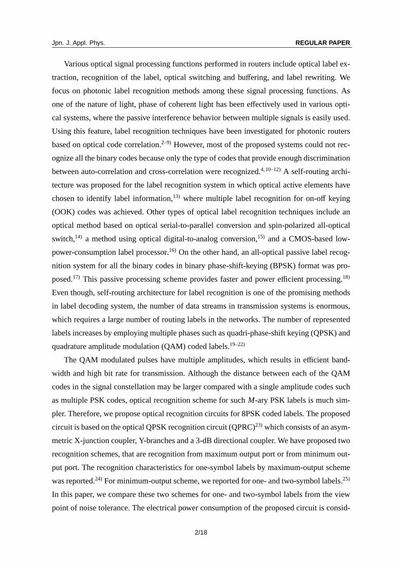
2.2.2 Minimum-output detection scheme Figure 8 shows a two-symbol recognition
circuit by the minimum-output detection scheme. The circuit has a two-stage connection of
the 8PRCs. The first symbol pulseEin1 is incident into the first stage 8PRC, 8PRC 1-1. The
reference pulse is amplified with an amplitude amplification coefficient of√
2 and divided
into two pulses. The reference signal amplitude at the input port of 8PRC 1-1 is the same as
Eref. The divided reference signal is amplified with an amplitude coefficient ofα2, and divided
into eight signals. These divided eight signals are added to the outputs of 8PRC 1-1, and sent
to the second-stage 8PRCs as the reference signals. The second symbol pulse is divided into
eight signals to the second-stage 8PRCs asE(k)in2.
The outputs from the second-stage 8PRC 2-k are calculated as follows by using eqs.(4)
and (7): E(8(k−1)+1)
out2...
E(8(k−1)+8)out2
= A8PRC
E0
2√
2ejmπ/4
E(1)out k +
α2E0
2√
2
. (9)
It is noted that the phase adjustment circuit is not employed after 8PRC 1-1 since the null
output from 8PRC 1-1 is used for a part of the reference signal to the second-stage 8PRCs.
The amplification coefficientα2 is found to be set asα2 =√
2 for the complete interference.
Fig. 9(a) shows the relative output intensities|E(i)out2/E0|2, (i = 1, . . . , 64) from the theo-
retical calculation for the casen = 0. The maximum output intensity is 0.160. Null outputs
are obtained at ports from 17 to 24 as shown in (b). The second minimum outputs appear
at ports from 49 to 56 and the intensity is 0.000785 (0.49 % of the maximum intensity).
9/18

Jpn. J. Appl. Phys. REGULAR PAPER
n
n
n
Fig. 9. Relative output intensities for two-symbol 8PSK labels by minimum-output detection for (a) output
port 1 to 64, (b) output port 17 to 24, and (c) output port 49 to 56.
This small second-minimum output is caused by the phase difference between the second
minimum outputE(k)out1 and the reference signal at the 2:1 combiners. This phase difference
cannot be compensated by a phase adjustment at the output of 8PRC 1-1 because there are
two phase-different second-minimum outputs for each 8PSK signal. If a phase adjustment is
employed forn = 0, the phase adjustment cannot adjust the phase for the othern. Therefore,
scalability for the minimum-output detection scheme is lower than that for the maximum-
output detection scheme. Nevertheless, the two-symbol 8PSK labels can be recognized by
thresholding the outputs between 0.000785 and 0.
3. Evaluation of Noise Tolerance
To investigate the noise tolerance for the proposed waveguide-type 8PRC, we built a simula-
tion model using OptiSytem software (Optiwave Systems Inc.). The waveguide-type QPRC
10/18

Jpn. J. Appl. Phys. REGULAR PAPER
E
E
E
E
E
E
Fig. 10. A simulation model for the waveguide-type QPRC module.
Ref
PRBS
PAM
PM
CW
laser
IM1
IM2
IM3
Proposed
8PSK
Recognition
Circuit
PD and
Post
processing
electric
circuit
Multi level
thresholder
PAM
decoder
BER
analyzer
f
Set
OSNR
Fig. 11. A simulation setup for one-symbol 8PSK recognition circuit.
module as illustrated in Fig. 3 is modeled with discrete optical components as shown in
Fig. 10. The module consists of two 3-dB directional couplers, two power dividers, a−π/2phase shifter, and aπ/2 phase shifter.
The simulation setup for one-symbol label recognition is illustrated in Fig. 11. A pseudo-
random-bit sequence (PRBS) with length of 214 − 1 is used for generating nonreturn-to-zero
(NRZ) sequence at a half of the bit rateR0 for 8PSK signals. The sequence signal is connected
to a serial-to-parallel (S/P) converter to make a sequence of 3-bit parallel signals. At the
same time, a reference signal is generated by a user defined bit sequence generator with
the same bit rate as that of the data signal and is connected to another S/P converter. A
parallel-to-serial (P/S) converter is used to combine a data signal and a reference signal.
The combined sequence is connected to a pulse-amplitude-modulator (PAM) to generate a
modulation electric signal. To generate the optical 8PSK coded signal, we use a continuous
wave (CW) laser at a frequency of 193.1 THz as a light source, a phase modulator (PM),
and an intensity modulator (IM1) to carve the NRZ to the return-to-zero (RZ) pulse train.
11/18

Jpn. J. Appl. Phys. REGULAR PAPER
Ref
PRBS
PAM
PM
CW
laser
IM1
IM2
IM4
PD and
Post
processing
electric
circuit
Multi level
thresholder
PAM
decoder
BER
analyzer
f
Set
OSNRIM3
Proposed
two symbol
8PSK
Recognition
Circuit
Fig. 12. A simulation setup for two-symbol 8PSK recognition circuit.
The component, named as Set OSNR, is used to add noise to the sequential train of the
8PSK pulse and the reference pulse. The noise added signals are sent to a serial to parallel
conversion circuit which consists of two intensity modulators and two delay elements. The
converted parallel 8PSK pulse train and the reference pulse train are incident to the proposed
label recognition circuit.
Practically, optical thresholders are used to identify the maximum or minimum port after
the optical recognition circuit. We employ the photodiodes (PDs) and postprocessing electric
circuit instead of the optical thresholders to measure the BER to evaluate the noise tolerance
in this study The circuits for the PDs and post-processing electric circuit differ in the two
recognition schemes as described in the next subsections.
Figure 12 illustrates the simulation setup for two-symbol label recognition. A two-symbol
8PSK pulse sequence is combined with a sequence of the reference signal to generate the
transmission pulse sequence. The received pulse sequence is converted to parallel pulse trains
and sent to the proposed recognition circuit.
The constellation for typical generated 8PSK signals at OSNR of 30 dB and 20 dB is
shown in Fig. 13.
3.1 Maximum-output detection scheme
The PDs and post-processing electric circuit for one-symbol 8PSK signals are shown in
Fig. 14. The input signals detected by PDs are filtered by the low pass filter (LPF) with cutoff
frequency of the symbol rate (= R0/3), and are amplified. The amplified electric signals are
12/18

Jpn. J. Appl. Phys. REGULAR PAPER
Fig. 13. Constellation for generated 8PSK signals at OSNR of (a) 30 dB and (b) 20 dB.
E
E
E
Fig. 14. The PDs and post-processing electric circuit for one-symbol 8PSK signals in the maximum-output
scheme.
sent to the thresholders to extract maximum signal pulses. The amplitudes of the thresholded
pulses are converted to different amplitudes by using the 1 to decimal converters to distin-
guish the output port of the 8PRC. Eight output signals from the postprocessing circuit are
added to convert into binary codes with the PAM decoder. The output codes are compared
with the incident data sequence to measure the BER by the BER analyzer. Typical signals
along the recognition circuit are shown in Fig. 15, where (a) a generated combined pulse se-
quence for the 8PSK signal and the reference signal, (b) the phase of pulses shown in (a), (c)
an output signal from the output port 1 of the 8PRC, (d) an output signal from output port 1
of the postprocessing circuit, and (e) an input signal to the final PAM decoder. The threshold
level in the postprocessing circuit was set at an electrical voltage corresponding to the optical
power of 0.368 mW which is in the middle of the maximum and the second maximum optical
power from the 8PRC of 0.397 mW and 0.339 mW, respectively. This threshold value was
chosen to optimize the BER performance.
The simulated BER performance as a function of OSNR at the receiver is shown in
13/18

Jpn. J. Appl. Phys. REGULAR PAPER
Fig. 15. Typical signals along the recognition circuit; (a) a generated combined pulse sequence for the
8PSK signal and the reference signal, (b) the phase of pulses shown in (a), (c) an output signal from the output
port 1 of the 8PRC, (d) an output signal from output port 1 of the postprocessing circuit, and (e) an input signal
to the final PAM decoder.
Fig. 16. BER performance for one- and two-symbol 8PSK labels by maximum output detection scheme.
Fig. 16. As a comparison, a BER measured by back-to-back (B2B) configuration is plotted by
using a digital coherent receiver with adaptive equalization, frequency offset estimation, and
carrier phase recovery. The BER performances at the bit rateR0 of 7.5, 15, and 30 Gb/s are
plotted. The required OSNR, for example, at BER of 1.0×10⁻³ atR0 = 7.5 Gb/s is around 22
dB and 24.5 dB for 1-symbol and 2-symbol length signals, respectively. As compared with
B2B BER performance, the required OSNR penalties of the proposed recognition circuit for
1-symbol and 2-symbol length signals at 7.5 Gb/s are around 15.5 dB and 18 dB, respectively.
The required OSNR becomes larger by 3 dB when the bit rate is doubled.
14/18

Jpn. J. Appl. Phys. REGULAR PAPER
E
E
E
Fig. 17. The PDs and post-processing electric circuit for one-symbol 8PSK signals in the minimum-output
scheme.
Fig. 18. Typical signals along the recognition circuit;(a) an output signal from the output port 1 of the
8PRC, (b) an output signal from the output port 12 of the 8PRC, (c) an output signal from output port 1 of the
postprocessing circuit, and (d) an output signal from output port 2 of the postprocessing circuit.
3.2 Minimum-output detection scheme
The PDs and post-processing circuit for the minimum-output scheme is shown in Fig. 17.
Electrical inverters are inserted in this circuit. Typical signals along the recognition circuit
for the input pulse sequence as illustrated in Figs. 15(a) and (b) is shown in Fig. 18, where (a)
an output signal from the output port 1 of the 8PRC, (b) an output signal from the output port
12 of the 8PRC, (c) an output signal from output port 1 of the postprocessing circuit, and (d)
an output signal from output port 2 of the post-processing circuit. As seen from Figs. 18(c)
and (d), repeated pulses were occurred at every two time slots corresponding to the time slots
for the reference pulses. These repeated pulses cancel out by summing all the outputs from
the post-processing circuit because the amplitudes of these pulses are -7, -5, -3, -1, 1, 3, 5,
and 7 as shown in Fig. 17. Thus, the input signal to the final PAM decoder is the same as
shown in Fig. 15(e).
15/18

Jpn. J. Appl. Phys. REGULAR PAPER
Fig. 19. BER performance for one- and two-symbol 8PSK labels by minimum output detection scheme.
The simulated BER performance as a function of OSNR at the receiver is shown in
Fig. 19. The required OSNR at BER of 1.0 × 10⁻³ at R0 = 7.5 Gb/s is around 14.5 dB
and 26.8 dB for 1-symbol and 2-symbol length signals, respectively. As compared with B2B
BER performance, the required OSNR penalties of the proposed circuit for 1-symbol and
2-symbol length signals at 7.5 Gb/s are around 8 dB and 18.3 dB, respectively. The required
OSNR becomes larger by 3 dB when the bit rate is doubled.
Despite the better BER performance than that of the maximum-output scheme for the one-
symbol signal, the performance becomes worse for the two-symbol signal. The reason for this
lower scalability for the minimum-output scheme was discussed in the previous section.
4. Conclusion
We have proposed the optical waveguide-type device for recognition of optical 8PSK coded
labels. The proposed device is based on the previously proposed waveguide-type circuit for
recognition of QPSK coded labels. The proposed device consists of 3dB directional cou-
plers, Y-branches, asymmetric X junction couplers, and a−π/4-phase shifter. The recogni-
tion method was theoretically discussed and the noise tolerance was also investigated. The
proposed circuit could recognize from either maximum or minimum output port. These two
recognition schemes were compared from the viewpoint of noise tolerance. The required
OSNR at BER of 1× 10⁻³ atR0 = 7.5 Gb/s was around 22 dB and 14.5 dB for the maximum
and minimum output schemes of one-symbol length 8PSK signals, respectively. The required
OSNR becomes larger by 3 dB when the bit rate is doubled.
We also discussed the scalability for the proposed recognition circuits. The maximum-
output detection scheme was found to be superior to the minimum-output one because the
phase adjustment cannot be employed between the first-stage 8PRC and the second-stage
8PRCs for the minimum-output detection circuit.
16/18

Jpn. J. Appl. Phys. REGULAR PAPER
References
1) A. E. Willner, S. Khaleghi, M. R. Chitgarha, M. R. Chitgarha, and O. F Yilmaz, J.
Lightwave Technol.,32(4), 660 (2013).
2) A. M. J. Koonen, N. Yan, J. J. V. Olmos, I. T. Monroy, C. Peucheret, E. V. Breusegem,
and E. Zouganeli, J. of Sel. Topics in Quantum Electron.,13(5), 1540 (2007).
3) S. J. B. Yoo, J. of Sel. Topics in Quantum Electron.,17(2), 406 (2011).
4) K. Kitayama, N. Wada, and H. Sotobayashi, J. Lightwave Technol.,18(12), 1834
(2000).
5) R. Clavero, J. M. Martinez, F. Ramos, and J. Marti, Opt. Express,12(18), 4326 (2004).
6) H. Furukawa, N. Wada, and T. Miyazaki, Optical Fiber Communication Conference
(OFC2006), OWP3 (2006).
7) N. Kataoka, G. Cincotti, N. Wada, and K. Kitayama, OptoElectronics and
Communication Conference (OECC2011), 8A2-5 (2011).
8) H. Brahmi, G. Giannoulis, M. Menif, V. Katopodis, D. Kalavrouziotis, C. Stamatiadis,
C. Kouloumentas, H. Avramopoulos, and D. Erasme, Photon. Technol. Lett.,24(9),
721(2012).
9) M. Xin, M. Chen, H. Chen, and S. Xie, Photon. Technol. Lett.,22(11) 769 (2010).
10) D. J. Blumenthal, B. E. Olsson, G. Rossi, T. E Dimmick, L. Rau, M. Masanovic, O.
Lavrora, R. Doshi, O. Jerphagnon, J. E. Bowers, and V. Kaman, J. Lighwave Technol.,
18(12), 2058 (2000).
11) O.Moriwaki, T. Kitoh, T. Sakamoto, and A. Okada, IEEE Photon. Technol. Lett.,17(2),
489 (2005).
12) G. Cincotti, J. Lightwave Technol.,22(2), 337 (2004).
13) I. Glesk, K. I. Kang, and P. R. Prucnal, Optics Express,1(5), 126 (1997).
14) R. Takahashi, T. Nakahara, H. Takenouchi, T. Yasui, and H. Suzuki, Optical Review,
11(2), 98 (2004).
15) K. Sawada and H. Uenohara, J. Lightwave Technol.,28(13) 1889 (2010).
16) S. Ibrahim, T. Nakahara, H. Ishikawa, and R. Takahashi, Opt. Express,24(7), 6985
(2016).
17) H. Hiura and N. Goto, IEICE Trans. Electron.,E90-C(8), 1619 (2007).
18) H. Hiura, J. Narita, and N. Goto, IEICE Trans. Electron.E90-C(12), 2270 (2007).
19) Y. Makimoto, H. Hiura, N. Goto, and S. Yanagiya, J. Ligthwave Technol.,27(1), 60
(2009).
17/18

Jpn. J. Appl. Phys. REGULAR PAPER
20) T. Surenkhorol, H. Kishikawa, N. Goto, and K. Gonchigsumlaa, Optical Engineering,
56(10), 107101 (2017).
21) K. Inoshita, H. Kishikawa, Y. Makimoto, N. Goto, and S. Yanagiya, “Proposal of
optical waveguide circuits for recognition of optical QAM codes,” J. Lightwave
Technol.,31(13), 2271-2278 (2013).
22) K. Inoshita, Y. Hama, H. Kishikawa, and N. Goto, Optical Engineering,55(12), 126105
(2016).
23) H. Hiura, N. Goto, and S. Yanagiya, J. Lighwave Technol.,27(24), 5543 (2009).
24) N. Odbayar, M. Adiya, H. Kishikawa, and N. Goto, CLEO Pacific Rim 2018
Conference (CLEO-pr2018), W4J.7 (2018).
25) M. Adiya, N. Odbayar, H. Kishikawa, and N. Goto, 23rd MicroOptics Conference
(MOC2018), J-3 (2018).
26) H. Kishikawa, Y. Makimoto, K. Inoshita, S. Igarashi, N. Goto, and S. Yanagiya, Optical
Engineering,55(5), 057104 (2016).
27) D. W. Stowe and T.-Y. Hsu, J. Lightwave Technol.,1(3), 519 (1983).
28) G. A. Berenbrock and B. Schlemmer, IEEE Photon. Tech. Lett.,1(4), 86 (1989).
I
18/18