wafer bonded 1.55 µm vertical cavity laser arrays for
TRANSCRIPT
University of California, Santa Barbara
Wafer Bonded 1.55 µm Vertical Cavity Laser Arrays
for Wavelength Division Multiplexing
By Adil M. Karim
A dissertation submitted in partial satisfaction of the requirements for the degree of
Doctor of Philosophy in Electrical and Computer Engineering
Committee in Charge:
Professor John E. Bowers, Chairperson Professor Daniel J. Blumenthal
Professor Larry A. Coldren Professor Evelyn L. Hu
December 2001

The dissertation of Adil M. Karim is approved
Professor Daniel J. Blumenthal
Professor Larry A. Coldren
Professor Evelyn L. Hu
Professor John E. Bowers, Chairperson
December 2001
ii
Wafer Bonded 1.55 µm Vertical Cavity Laser Arrays for Wavelength Division Multiplexing
Copyright by Adil Karim March 2001
Electrical and Computer Engineering Department University of California, Santa Barbara
Santa Barbara, CA 93106
iii

Acknowledgments
“No man is an island, entire of itself; every man is a piece of the
continent, a part of the main…”
John Donne’s words are as relevant in our time as they were in his own.
The work described in this dissertation was made possible by a number of
individuals. Professor John Bowers taught me about lasers, life and the
NASDAQ. I will always be grateful to him for his stalwart support and his
willingness to let me follow my own ideas. Professors Blumenthal, Coldren and
Hu provided valuable support and keen insight. Their contributions are gratefully
recognized.
I have followed a long and distinguished line of wafer-bonded VCSEL
makers at UCSB. Jim Dudley, Dubravko Babic, Near Margalit and Alexis Black
paved the way for me. I thank you for your ideas, your fellowship and leaving
something for me to do. I am indebted to many other members of the UCSB
family. Jack Whaley, Bob Hill and Martin Vandenbroek went above and beyond
the call of duty in maintaining cleanroom facilities. The dark arts of crystal
growth are beyond my ken. Patrick Abraham, Yae Okuno, Dan Lofgreen and Yi-
Jen Chiu grew numerous wafers for me during my time at UCSB. Their efforts
iv

were invaluable. I was fortunate to be surrounded by an extraordinary group of
students and staff, in addition to those recognized above. Vickie Edwards, Eric
Hall, Volkan Kaman, Adrian Keating, Thomas Liljeberg, Bin Liu, Christina
Loomis, Joachim Piprek, Maura Raburn, Gerry Robinson, Kehl Sink, Daniel
Tauber, and Sheng Zhang were both teachers and colleagues. Staffan Björlin
became a member of the vertical cavity family and a good friend. I was privileged
to share my tenure at UCSB and a cubicle with Chris LaBounty. His assistance
with the thermal analysis in Chapter 5 is much appreciated. Daniel Green is a
trusted roommate, cleanroom vampire and voice of reason. I am grateful to
Rebecca Patterson for her friendship, support and understanding.
My family has been a source of love and gentle guidance throughout my
life. Robert and Virginia Lewis have been mentors to my family for three
generations. Their wisdom and warmth are inspirational. I thank my father,
Zubaid, for making me do my math homework and teaching me to be my best.
My mother, Saman, played catch with me, drove me to the library and let me find
my own way in life. Arif, my brother, still can’t beat me at sports video games.
But in every other way, he has become a remarkable young man who continues to
motivate and encourage me.
v

Dedicated to my family: past, present and future
vi
Vita
Education June 1996 B.S. with honors, Applied Physics California Institute of Technology June 1997 M.S., Optics University of Rochester December 2001 Ph.D., Electrical and Computer Engineering University of California, Santa Barbara Published Journal Papers [1-6] 1. A. Karim, J. Piprek, P. Abraham, D. Lofgreen, Y.J. Chiu and J.E. Bowers,
“1.55 µm vertical-cavity laser arrays for wavelength-division multiplexing,” IEEE Journal of Selected Topics in Quantum Electronics, vol. 7, pp. 178-183, 2001.
2. A. Karim, P. Abraham, D. Lofgreen, Y.J. Chiu, J. Piprek, and J.E. Bowers,
“Wafer bonded 1.55 µm vertical-cavity lasers with continuous-wave operation up to 105°C,” Applied Physics Letters, vol. 78, pp. 2632-3, 2001.
3. A. Karim, P. Abraham, D. Lofgreen, Y.J. Chiu, J. Piprek, and J.E. Bowers,
“Wafer bonded 1.55 µm vertical cavity laser arrays for wavelength division multiplexing,” Electronics Letters, vol. 37, pp. 431-2, 2001.
4. A. Karim, S. Björlin, J. Piprek, and J.E. Bowers, “Long wavelength
vertical cavity lasers and amplifiers,” IEEE Journal of Selected Topics in Quantum Electronics, vol. 6, pp. 1244-53, 2000. (invited)
5. A. Karim, K.A. Black, P. Abraham, D. Lofgreen, Y.J. Chiu, J. Piprek, and
J.E. Bowers, “Superlattice barrier 1528 nm vertical-cavity laser with 85°C continuous-wave operation,” IEEE Photonics Technology Letters, vol. 12, pp. 1438-40, 2000.
vii
6. A. Keating, A. Black, A. Karim, Y.J. Chiu, P. Abraham, C. Harder, E. Hu, and J.E. Bowers, “High-temperature optically pumped 1.55 µm VCSEL operating at 6 Gb/s,” IEEE Photonics Technology Letters, vol. 12, pp. 116-8, 2000.
Published Conference Proceedings and Presentations [7-15] 7. A. Karim, “Vertical cavity lasers for telecommunications networks:
prospects and challenges,” 2001 Digest of the LEOS Summer Topical Meetings, MA 3.1, July 30 – August 1, 2001, Copper Mountain, CO. (invited)
8. A. Karim, P. Abraham, D. Lofgreen, Y.J. Chiu, J. Piprek and J.E. Bowers,
“Superlattice barrier 1528 nm vertical cavity laser with 85°C continuous wave operation,” Conference Digest, 2000 IEEE 17th International Semiconductor Laser Conference, pp. 157-8, September 25-28, 2000, Monterey, CA.
9. A. Karim, P. Abraham, D. Lofgreen, Y.J. Chiu and J.E. Bowers, “Long
wavelength vertical cavity lasers for WDM applications,” 2000 IEEE 17th International Semiconductor Laser Conference, post-deadline session, September 25-28, 2000, Monterey, CA.
10. A. Karim, K.A. Black, E.S. Björlin, P. Abraham, Y.J. Chiu, J. Piprek, and
J.E. Bowers, “Long wavelength vertical cavity lasers and amplifiers,” Proceedings of 5th Optoelectronics and Communications Conference, July 10-14, 2000, Chiba, Japan. (invited)
11. A. Karim, K.A. Black, P. Abraham, D. Lofgreen, Y.J. Chiu, and J.E.
Bowers, “80°C CW operation of long wavelength VCSEL using a superlattice barrier,” Conference Proceedings of Twelfth International Conference on Indium Phosphide and Related Materials (IPRM ’00), post-deadline session, May 14-18, 2000, Williamsburg, VA.
viii

12. P. Abraham, K.A. Black, A. Karim, J. Piprek, Y.J. Chiu, B. Liu, A. Shakouri, S.K. Mathis, E.L. Hu, and J.E. Bowers "VCSEL and high-performance photonics enabled by wafer bonding," 5th International Symposium on Semiconductor Wafer Bonding Science, Technology and Applications, Electrochemical Society & Electrochemical Society of Japan 1999 Joint International Meeting, October 17-22, 1999, Honolulu, HI. (invited)
13. A. Keating, A. Black, A. Karim, Y.J. Chiu, P. Abraham, C. Harder, E. Hu,
J. Bowers, “6 Gbit/s optically pumped 1.55 µm VCSEL operating up to 105°C,” Proceedings of 25th European Conference on Optical Communications (ECOC ’99), vol. 2, pp. 298-9, September 27-30, 1999, Nice, France.
14. A. Keating, A. Black, A. Karim, Y.J. Chiu, P. Abraham, C. Harder, E. Hu,
J. Bowers, “High temperature, optically pumped, 1.55 µm VCSEL operating at 6 Gb/s,” 1999 57th Annual Device Research Conference Digest, vol. 2, pp. 196-7, June 28-30, 1999, Santa Barbara, CA.
15. K.A. Black, P. Abraham, A. Karim, J.E. Bowers and E.L. Hu, “Improved
luminescence from InGaAsP/InP MQW active regions using a wafer fused superlattice barrier,” Conference Proceedings of Eleventh International Conference on Indium Phosphide and Related Materials (IPRM ’99), pp. 357-60, May 16-20, 1999, Davos, Switzerland.
ix

x
Abstract Wafer Bonded 1.55 µm Vertical Cavity Laser Arrays for Wavelength
Division Multiplexing
Adil M. Karim
Vertical cavity lasers in the 1.55 µm wavelength band are attractive
sources for optical networks. Previous devices have been limited by low output
power and poor thermal performance. In this work, novel wafer bonding
techniques were developed to create high-performance 1.55 µm vertical cavity
lasers and a new class of multiple wavelength vertical cavity laser arrays. Wafer
bonding enables the integration of thermally conductive GaAs/AlGaAs mirrors
and traditional InP/InGaAsP active regions. A superlattice barrier was used as a
buffer layer during bonding to reduce the number of non-radiative recombination
centers in the active region. The surface of these superlattice layers was patterned
prior to bonding to define multiple wavelength cavities. Continuous-wave
operation was achieved at temperatures up to 105°C. This is the highest reported
lasing temperature for a 1.55 µm vertical cavity laser. Threshold currents of 0.8
mA were measured. The peak output power at 20°C was 0.7 mW. The peak
output power at 80°C was 0.2 mW. Single-mode operation with a side-mode
suppression ration in excess of 40 dB was observed for a 5 µm aperture device.
Four-channel arrays were also fabricated. The wavelength span was 1509.1-
1524.4 nm with channel spacing of approximately 5 nm. This is the first
demonstration of an independently addressable, multiple-wavelength vertical
cavity laser array at 1.55 µm. Threshold currents of 1.0 mA and peak output
powers of 0.5 mW were measured for array elements. Thermal and optical
crosstalk between array elements are negligible, due to the high thermal
conductivity of the bottom mirror and large device pitch.

Chapter 1: Introduction
1. Introduction 1.1. Overview
This thesis makes significant contributions in the areas of wafer bonding
and long wavelength vertical-cavity surface-emitting laser (VCSEL)
development. A superlattice buffer layer was introduced in order to preserve
material quality through the bonding process, resulting in improved
photoluminescence from bonded quantum well structures. This technique was
used to fabricate high performance 1.55 um VCSELs with the highest continuous
wave operating temperatures reported to date. Intracavity tuning layers were
patterned prior to bonding in order to define multiple wavelength VCSEL
cavities. This approach was used to create the first independently addressable
VCSEL array for wavelength division multiplexing at 1.55 µm.
In this chapter, the basic motivation for long wavelength VCSEL
fabrication is explored. The favorable aspects of the vertical cavity geometry are
presented. Although there are challenges in extending the success of short
wavelength VCSELs to longer wavelengths, the need for low cost, high
performance sources in optical networks has driven long wavelength VCSEL
development. The suitability of 1.55 µm VCSELs and multiple wavelength
1

Chapter 1: Introduction
VCSEL arrays for local and metropolitan area networks is discussed. Finally, the
remaining chapters in the dissertation are outlined.
1.2. Vertical Cavity Surface Emitting Lasers
Vertical cavity surface emitting lasers have been studied extensively in
recent years for use in fiber optic networks and as optical interconnects. The
VCSEL offers many potential advantages when compared to the traditional edge-
emitting laser. The most recognized advantage of the VCSEL is compatibility
with low cost wafer scale fabrication and testing methods. High volume, low cost
manufacturing is of vital importance for the next generation of photonic devices.
The VCSEL has several other characteristics that make it well-suited for use in
fiber optic systems. These include a circular output beam for high coupling
efficiency into optical fiber, high modulation bandwidths at low currents, single
mode operation, low power consumption and the potential for producing
integrated modules and arrays on wafer.
VCSEL
s
Figure 1.1 Schematic of edge-emitting and vertical cavity surface-emitting laser
Edge-emitting
2

Chapter 1: Introduction
Edge-emitting lasers emit light in a direction parallel to the host substrate.
The rectangular waveguide supports an elliptical transverse mode. This elliptical
beam is not easily coupled into standard optical fiber, resulting in coupling
efficiencies of 20-50% for most designs. An additional lens element may be
introduced to improve coupling efficiency to above 70%. However, this increases
the cost of the laser and complicates packaging. The devices are formed by
cleaving the processed wafer into individual devices. The cleaving process
determines the size of the laser cavity and defines the laser mirrors formed by the
semiconductor-air interface. Typical edge-emitters are less than 10 µm wide and
under 1000 µm in length. Cleaving of individual laser die is a time- and labor-
intensive process. The limited yield forces prices upward and increases the lead
time of new devices. Testing expenses are high due to labor costs, complications
associated with handling small device die and inability to select successful
devices until after cleaving. Advanced cavity designs such as distributed Bragg
reflector (DBR) and distributed feedback (DFB) lasers offer high single-mode
powers for increased performance, but require complicated regrowths that further
limit production volumes. Despite these manufacturing limitations, edge-emitting
lasers are widely used in lightwave systems and are the dominant sources for
transmission at the telecommunications wavelengths of 1300 and 1550 nm.
3

Chapter 1: Introduction
The vertical cavity geometry found in VCSELs offers significant
manufacturing advantages compared to traditional edge-emitting lasers and also
has the potential for increased functionality at lower cost. As seen in Figure 1.1,
the VCSEL cavity is defined by top and bottom mirrors in a direction
perpendicular to the substrate. These mirrors contain a number of quarter-wave
layers and are known as distributed Bragg reflectors (DBRs). These multilayer
films are required in order to provide the high reflectivities required in a VCSEL,
typically greater than 99%. Because the processed wafer contains discrete devices
without the burden of an additional cleaving step, devices may be tested with a
probe card on wafer prior to packaging. This streamlines the production and
testing processes compared to those used for edge-emitting lasers. Light-emitting
diodes (LEDs) have similar manufacturing advantages, but are limited to low-
speed, short distance optical links due to poor frequency response and large
spectral width. The VCSEL geometry allows for close packing of devices, with up
to 30,000 conservatively spaced devices possible on a 2” wafer. This density may
be increased even further for applications such as laser printing and optical
storage.
If VCSEL wafers are cleaved into individual devices, some of the same
difficulties are encountered as with edge-emitting devices. However, one of the
4

Chapter 1: Introduction
principal VCSEL advantages lies in the simple formation of one and two-
dimensional arrays. These arrays significantly reduce packaging costs by
integrating multiple devices on a single die without any manual assembly. Etched
cylindrical waveguides may easily be introduced on the VCSEL wafer to produce
a circular spot for efficient coupling into standard single-mode or multi-mode
fiber. Coupling efficiencies of 90% for multimode fiber and 80% for single-mode
fiber have been reported using simple butt-coupling without additional optics[1-
3]. The selective lateral oxidation of a layer in the VCSEL structure may be used
to provide transverse electrical and optical confinement[4]. The oxide aperture
funnels the current into a small area for efficient lasing by providing local
electrical isolation. The aperture also provides lateral optical confinement by
acting as an intracavity lens, reducing optical losses due to scattering and
diffraction[5]. This technique of index guiding can be used to control the output
mode profile[6]. Current confinement may also be achieved through the use of ion
implantation[7]. By confining the injected current, the lasing action is limited to a
small area by gain guiding. In this case, thermal lensing is the primary contributor
to lateral index guiding[8].
The active region volume in a VCSEL is typically smaller than that of an
edge-emitting laser, leading to reduced threshold currents[9]. This lower modal
5

Chapter 1: Introduction
volume permits high modulation bandwidths at low current levels[10-13].
Optoelectronic integrated circuits (OEICs) featuring VCSELs and transistors
fabricated from a common epitaxial structure have been reported[14-16]. These
low cost modules have several potential applications in optical communications.
Arrays of VCSELs can be used for parallel signal processing[17]. VCSELs may
also be integrated with photodetectors[18, 19] for bi-directional optical
interconnects.
1.3. Long Wavelength VCSELs
Rapid progress in VCSEL development over the last decade has allowed
850 and 980 nm devices to be deployed in optical networks. The use of ion
implantation for current confinement has permitted the manufacture of highly
efficient planar devices[20]. The selective oxidation of AlGaAs alloys[21] has
enabled major advances in threshold current and wallplug efficiency[22]. In short-
haul applications such as Fibre Channel and Gigabit Ethernet (GbE), the
efficiency and high speed at low power of 850-980 nm GaAs-based VCSELs have
made them the light source of choice. However, for longer reach applications,
long wavelength (1.3-1.6 µm) laser diodes are required. Using 1.3 and 1.55 µm
sources over single-mode fiber significantly reduces attenuation and dispersion in
optical links. It can be seen in Figure 1.2 that long wavelength lasers at 1.3 and
6

Chapter 1: Introduction
1.55 µm permit higher bit rates over longer distances than lasers emitting at 0.85
or 0.98 µm. The graph shown below assumes an input power of 1 mW and uses
common parameters for single-mode and graded-index fiber. The model includes
attenuation and dispersion, but non-linear effects such as chirp have been
neglected.
0.1
1
10
100
1000
0.0001 0.001 0.01 0.1 1 10 100
Bit rate (Gb/s)
Dis
tanc
e (k
m)
1.55 µm, single-mode fiber
1.3 µm, single-mode fiber
0.98 µm, graded-index fiber
0.85 µm, graded-index fiber
Figure 1.2 Fiber optic transmission limits for 1.55, 1.3, 0.98, and 0.85 µm
Emerging standards such as 10 Gigabit Ethernet (10 GbE) are expected to
drive the market for low-cost optical transceivers capable of high-speed
7

Chapter 1: Introduction
transmission over distances of more than 10 km. It is expected that 10 GbE will
find acceptance in local area networks (LANs), metropolitan area networks
(MANs) and even wide area networks (WANs). This developing standard will
specify protocols for a new generation of optical Ethernet. Applications such as
LAN to LAN interconnects, broadband virtual private networks (VPNs) and high
speed Internet access will see dramatic performance improvements as products
based on 10 GbE become available. 10 GbE traffic may be offered with
asynchronous transfer mode (ATM), frame relay (FR) and other services, and
transported directly over existing synchronous optical network (SONET) links.
This helps to ensure efficient use of bandwidth. 10 GbE can itself be used to
combine slower access links at the WAN interface.
These new services will become particularly crucial in metropolitan area
networks. Although high-performance optical transport solutions have become
more common in recent years, these systems are more relevant for long haul
transmission and are not generally cost-effective for MANs. The high traffic
demands at the metropolitan core include services such as digital subscriber line
(DSL), cable modems and streaming video. Multiple wavelengths may be used in
order to circumvent fiber exhaust. The highly aggregated nature of metropolitan
core traffic requires that these services be provided at full data rates. These new
8
Chapter 1: Introduction
metropolitan services may be provided over dedicated wavelengths or shared
wavelengths, using time-division multiplexing (TDM). The first draft of the 10
GbE standard calls for four different physical interfaces, but other interfaces may
also eventually be ratified by the expected completion date of 2002. Current
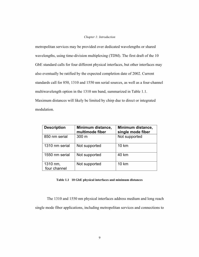
standards call for 850, 1310 and 1550 nm serial sources, as well as a four-channel
multiwavelength option in the 1310 nm band, summarized in Table 1.1.
Maximum distances will likely be limited by chirp due to direct or integrated
modulation.
Description Minimum distance, multimode fiber
Minimum distance, single mode fiber
850 nm serial 300 m Not supported
1310 nm serial Not supported 10 km
1550 nm serial Not supported 40 km
1310 nm, four channel
Not supported 10 km
s
The 1
single mode
Table 1.1 10 GbE physical interfaces and minimum distance
310 and 1550 nm physical interfaces address medium and long reach
fiber applications, including metropolitan services and connections to
9

Chapter 1: Introduction
optical networks. Inexpensive sources such as long wavelength VCSELs are ideal
for enabling this next generation of access and backbone technology.
Long wavelength VCSELs are anticipated as sources in other networks as
well, including intrasystem links, VSR (very short reach) SONET interfaces, and
cable television (CATV) distribution. High performance, single mode devices are
slotted for insertion into long haul and metropolitan fiber spans. 1.55 µm VCSELs
in the local and metropolitan area network offer the additional benefit of
interoperability with the 1.55 µm networks used for long haul transmission. These
improvements in performance will be made more accessible by the VCSEL
fabrication advantages discussed earlier. In addition, higher signal powers will be
permitted due to reduced eye safety risks, since source wavelengths have been
pushed further into the infrared. This extends both the reach and functionality of
optical modules. Lower voltage operation should also be possible due to the
narrower bandgap of long wavelength materials. This reduces power
consumption, allowing for simpler drive circuitry and packaging.
1.4. Obstacles to Development
Despite the obvious commercial incentives, long wavelength VCSELs
have been slower to develop than their short wavelength counterparts. The main
10
Chapter 1: Introduction
limitation has been unsatisfactory mirror performance. Distributed Bragg
reflectors (DBRs) with high thermal conductivity, high reflectivity, and, in the
case of current injection through the DBR, high electrical conductivity have
proven difficult to fabricate on InP. Poor mirror performance results in low output
power and unsatisfactory high temperature operation. Only a limited number of
designs have been shown to lase continuous-wave at room temperature.
Maximum ambient operating temperatures of 70-85°C are specified by Telcordia
for sources in fiber optic networks. In order for VCSELs to maintain their cost
advantage over edge-emitting lasers, they must be able to operate at these
elevated temperatures without thermoelectric coolers.
The most common materials used for 1.3 and 1.55 µm lasers are InP and
InGaAsP, grown on InP substrates. Inherent material qualities of InP/InGaAsP
such as low characteristic temperatures, high Auger recombination rates and high
intervalence band absorption[23] have slowed long wavelength VCSEL
development. The lack of a robust aperturing technique on InP similar to the
lateral oxidation of AlGaAs on GaAs has also limited the operating efficiency.
A number of novel designs have been developed to overcome the
limitations of the traditional InGaAsP material system. These include AlInGaAs
11
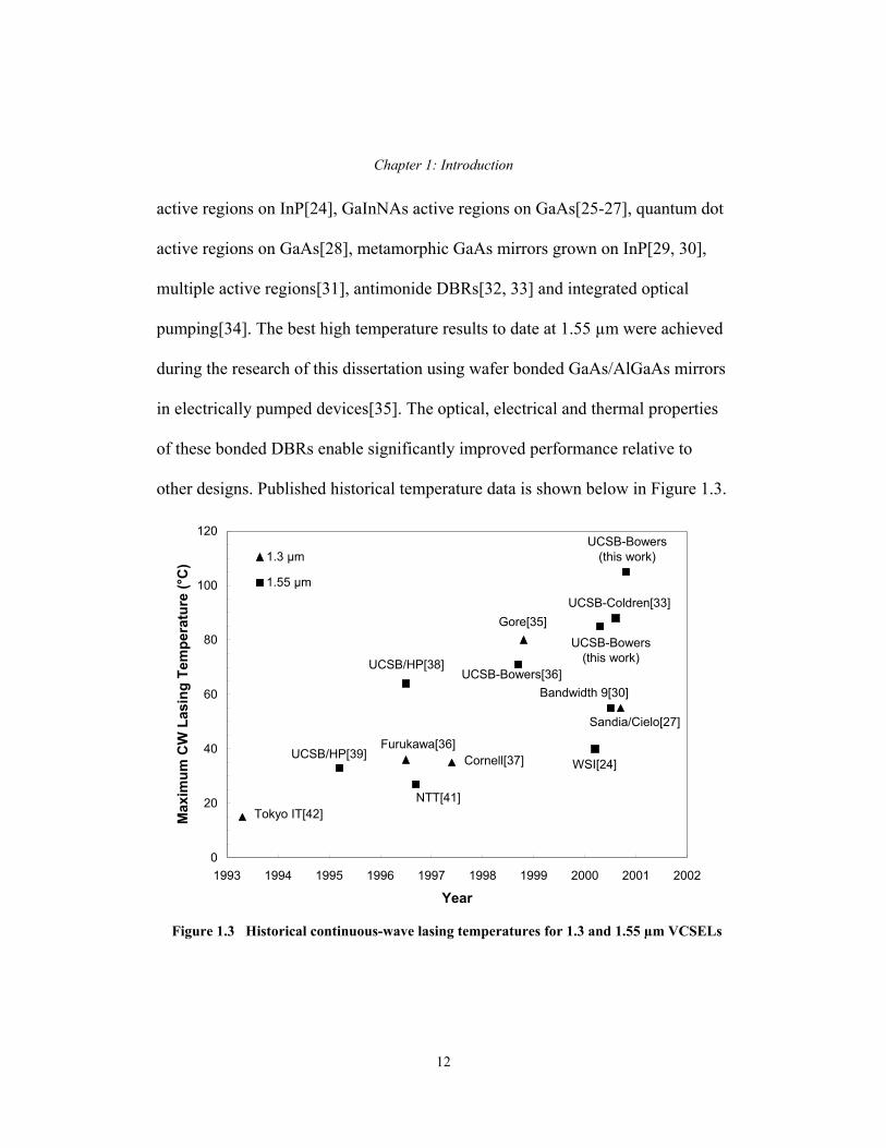
Chapter 1: Introduction
active regions on InP[24], GaInNAs active regions on GaAs[25-27], quantum dot
active regions on GaAs[28], metamorphic GaAs mirrors grown on InP[29, 30],
multiple active regions[31], antimonide DBRs[32, 33] and integrated optical
pumping[34]. The best high temperature results to date at 1.55 µm were achieved
during the research of this dissertation using wafer bonded GaAs/AlGaAs mirrors
in electrically pumped devices[35]. The optical, electrical and thermal properties
of these bonded DBRs enable significantly improved performance relative to
other designs. Published historical temperature data is shown below in Figure 1.3.
0
20
40
60
80
100
120
1993 1994 1995 1996 1997 1998 1999 2000 2001 2002
Year
Max
imum
CW
Las
ing
Tem
pera
ture
(°C
) 1.3 µm
1.55 µm
Tokyo IT[42]
UCSB/HP[39]
NTT[41]
Furukawa[36]Cornell[37]
UCSB/HP[38]
WSI[24]
UCSB-Bowers[36]
Gore[35]
UCSB-Bowers(this work)
UCSB-Bowers(this work)
UCSB-Coldren[33]
Bandwidth 9[30]
Sandia/Cielo[27]
s
Figure 1.3 Historical continuous-wave lasing temperatures for 1.3 and 1.55 µm VCSEL
12

Chapter 1: Introduction
1.5. Wavelength Division Multiplexing
An explosion in consumer demand for bandwidth has forced many service
providers to cope with fiber exhaust. Wavelength division multiplexing (WDM)
permits the increase of transmission capacity by using multiple channels operating
at different wavelengths. This allows for increased transmission rates without the
time and expense of installing additional fiber spans. Sending multiple signals on
different wavelengths down a single fiber allows improved bandwidth
management, including wavelength routing and reconfiguration. An illustration of
the WDM process is shown in Figure 1.4.
B bits/sec, λ1
B bits/sec, λ2
B bits/sec, λ3
B bits/sec, λ4
4B bits/sec
λ1, λ2, λ3, λ4
0
0.5
1
0 20 40 60 80
Wavelength
Pow
er
λ1 λ2 λ3 λ4
B bits/sec, λ1
B bits/sec, λ2
B bits/sec, λ3
B bits/sec, λ4
4B bits/sec
λ1, λ2, λ3, λ4
0
0.5
1
0 20 40 60 80
Wavelength
Pow
er
λ1 λ2 λ3 λ4100100
Figure 1.4 Wavelength division multiplexing with four channels
13
Chapter 1: Introduction
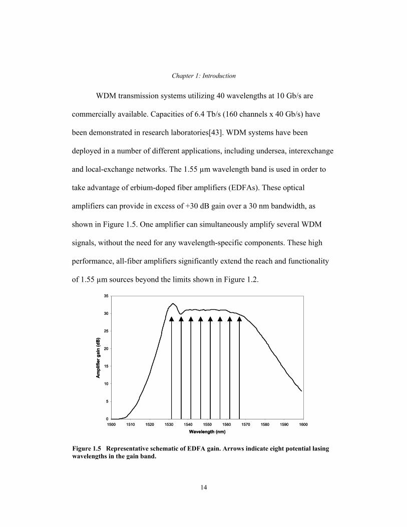
WDM transmission systems utilizing 40 wavelengths at 10 Gb/s are
commercially available. Capacities of 6.4 Tb/s (160 channels x 40 Gb/s) have
been demonstrated in research laboratories[43]. WDM systems have been
deployed in a number of different applications, including undersea, interexchange
and local-exchange networks. The 1.55 µm wavelength band is used in order to
take advantage of erbium-doped fiber amplifiers (EDFAs). These optical
amplifiers can provide in excess of +30 dB gain over a 30 nm bandwidth, as
shown in Figure 1.5. One amplifier can simultaneously amplify several WDM
signals, without the need for any wavelength-specific components. These high
performance, all-fiber amplifiers significantly extend the reach and functionality
of 1.55 µm sources beyond the limits shown in Figure 1.2.
0
5
10
15
20
25
30
35
1500 1510 1520 1530 1540 1550 1560 1570 1580 1590 1600
Wavelength (nm)
Am
plifi
er g
ain
(dB
)
0
5
10
15
20
25
30
35
1500 1510 1520 1530 1540 1550 1560 1570 1580 1590 1600
Wavelength (nm)
Am
plifi
er g
ain
(dB
)
Figure 1.5 Representative schematic of EDFA gain. Arrows indicate eight potential lasing wavelengths in the gain band.
14

Chapter 1: Introduction
Multiple laser wavelengths are required to launch signals in WDM
systems. Channel spacing can range from greater than 10 nm for coarse WDM
(CWDM) to less than 0.2 nm for dense WDM (DWDM). These sources are
typically individual edge-emitting DFB lasers, packaged together as a module.
Using VCSELs as sources in WDM networks would reduce transmitter cost and
complexity. The VCSEL fabrication advantages described in Section 1.1 could be
used to lower the cost of each individual laser. However, a multiple-wavelength
VCSEL array fabricated on a single substrate would further reduce costs by
eliminating the complex assembly of individual lasers in WDM transmitter
modules. This becomes even more critical as WDM systems extend their reach to
metropolitan and local area networks, where cost concerns are paramount.
Considering both cost and performance, one and two dimensional multiple-
wavelength VCSEL arrays emitting in the 1.55 µm wavelength region are highly
attractive sources for low cost WDM networks.
1.6. Overview of Dissertation
This dissertation describes the design, processing and testing of wafer
bonded 1.55 µm VCSELs and WDM VCSEL arrays. The wafer bonding
technique is used in order to integrate high quality GaAs-based mirrors with
conventional InP-based active regions. Theory, design and results from two
15

Chapter 1: Introduction
different device generations are presented. This work makes contributions in a
number of areas, including wafer bonding, fabrication of 1.55 µm VCSELs and
multiple wavelength VCSEL arrays, and wavelength division multiplexing.
Chapter 2 analyzes the distributed Bragg reflectors (DBRs) used as
mirrors in 1.55 µm VCSELs. Optical, electrical and thermal characteristics are
considered. Experimental results are compared with theory. The use of
GaAs/AlGaAs DBRs is motivated by the demonstrated need for high reflectivity,
low optical loss, low electrical resistance and high thermal conductivity.
Chapter 3 describes the wafer bonding process used to integrate
GaAs/AlGaAs DBRs with InP/InGaAsP active regions. A summary of bonding
results from UCSB and other institutions is presented. The bonding process itself
is described in detail. The electrical, optical and structural impacts of wafer
bonding are considered. The introduction of a superlattice barrier is shown to
reduce lattice defects and non-radiative recombination in bonded active regions.
Patterned bonding for the definition of multiple wavelength VCSEL cavities is
characterized.
16
Chapter 1: Introduction
Chapter 4 considers VCSEL device structure and fabrication. Basic
VCSEL design philosophy is presented. Different cavity designs and contacting
schemes are compared, taking optical and electrical considerations into account.
The VCSEL fabrication processes used during the course of this dissertation are
described.
Chapter 5 analyzes the characteristics of fabricated single-wavelength and
multiple-wavelength device structures. Parameters of interest include threshold
current, output power, and differential efficiency. Size and temperature
dependence are studied. Thermal and optical crosstalk are considered theoretically
and compared with experimental results. Current spreading and carrier leakage
are identified as performance-limiting mechanisms.
Chapter 6 summarizes the progress made during the course of this
dissertation. The emerging long wavelength VCSEL market is discussed. Future
work aimed at continued device development and optimization of existing devices
is proposed.
17

Chapter 1: Introduction
References
[1] J. Heinrich, E. Zeeb, and K. J. Ebeling, "Butt-coupling efficiency of
VCSELs into multimode fibers," IEEE Photonics Technology Letters, vol.
9, pp. 1555-7, 1997.
[2] P. Schnitzer, M. Grabherr, R. Jager, J. Joos, C. Jung, R. King, R.
Michalzik, W. Schmid, D. Wiedenmann, and K. J. Ebeling, "High
performance VCSEL arrays for optical interconnection," Proceedings of
48th ECTC, pp. 762-70, 1998.
[3] V. Jayaraman, J. C. Geske, M. MacDougal, F. Peters, T. Lowes, T. Char,
D. Van Deusen, T. Goodnough, M. Donhowe, S. Kilcoyne, and D. Welch,
"Long-wavelength vertical-cavity laser research at Gore," Proceedings of
the SPIE, vol. 3627, pp. 29-37, 1999.
[4] K. D. Choquette, K. L. Lear, R. P. Schneider, and K. M. Geib, "Cavity
characteristics of selectively oxidized vertical-cavity lasers," Applied
Physics Letters, vol. 66, pp. 3413-15, 1995.
[5] L. A. Coldren, B. J. Thibeault, E. R. Hegblom, G. B. Thompson, and J. W.
Scott, "Dielectric apertures as intracavity lenses in vertical-cavity lasers,"
Applied Physics Letters, vol. 68, pp. 313-15, 1996.
18

Chapter 1: Introduction
[6] K. L. Lear, K. D. Choquette, R. P. Schneider, Jr., and S. P. Kilcoyne,
"Modal analysis of a small surface emitting laser with a selectively
oxidized waveguide," Applied Physics Letters, vol. 66, pp. 2616-18, 1995.
[7] S. J. Pearton, "Ion implantation in III-V semiconductor technology,"
International Journal of Modern Physics B, vol. 7, pp. 4687-761, 1993.
[8] M. Brunner, K. Gulden, R. Hovel, M. Moser, and M. Ilegems, "Thermal
lensing effects in small oxide confined vertical-cavity surface-emitting
lasers," Applied Physics Letters, vol. 76, pp. 7-9, 2000.
[9] D. G. Deppe, D. L. Huffaker, O. Tchang-Hun, D. Hongyu, and D. Qing,
"Low-threshold vertical-cavity surface-emitting lasers based on oxide-
confinement and high contrast distributed Bragg reflectors," IEEE Journal
of Selected Topics in Quantum Electronics, vol. 3, pp. 893-904, 1997.
[10] Y. Satuby and M. Orenstein, "Limits of the modulation response of a
single-mode proton implanted VCSEL," IEEE Photonics Technology
Letters, vol. 10, pp. 760-2, 1998.
[11] B. J. Thibeault, K. Bertilsson, E. R. Hegblom, E. Strzelecka, P. D. Floyd,
R. Naone, and L. A. Coldren, "High-speed characteristics of low-optical
loss oxide-apertured vertical-cavity lasers," IEEE Photonics Technology
Letters, vol. 9, pp. 11-13, 1997.
19

Chapter 1: Introduction
[12] K. L. Lear, V. M. Hietala, H. Q. Hou, J. Banas, B. E. Hammons, J. Zolper,
S. P. Kilcoyne, M. Nuss, and J. Bowers, "High-speed 850 nm oxide-
confined vertical cavity surface emitting lasers," OSA Trends in Optics
and Photonics, vol. 13, pp. 80-2, 1997.
[13] F. Mederer, C. Jung, R. Jager, M. Kicherer, R. Michalzik, P. Schnitzer, D.
Wiedenmann, and K. J. Ebeling, "12.5 Gbit/s data rate fiber transmission
using single-mode selectively oxidized GaAs VCSELs at λ =850 nm,"
1999 IEEE LEOS Annual Conference Proceedings, vol. 2, pp. 697-8 1999.
[14] Y. J. Yang, T. G. Dziura, T. Bardin, S. C. Wang, R. Fernandez, and A. S.
H. Liao, "Monolithic integration of a vertical cavity surface emitting laser
and a metal semiconductor field effect transistor," Applied Physics Letters,
vol. 62, pp. 600-2, 1993.
[15] P. Zhou, J. Cheng, J. C. Zolper, K. L. Lear, S. A. Chalmers, G. A. Vawter,
R. E. Leibenguth, and A. C. Adams, "Monolithic optoelectronic switch
based on the integration of a GaAs/AlGaAs heterojunction bipolar
transistor and a GaAs vertical-cavity surface-emitting laser," IEEE
Photonics Technology Letters, vol. 5, pp. 1035-8, 1993.
[16] U. Eriksson, P. Evaldsson, and K. Streubel, "Fabrication of a 1.55 µm
VCSEL and an InGaAsP-InP HBT from a common epitaxial structure,"
IEEE Photonics Technology Letters, vol. 11, pp. 403-5, 1999.
20

Chapter 1: Introduction
[17] M. W. Haney, M. P. Christensen, P. Milojkovic, J. Ekman, P.
Chandramani, R. Rozier, F. Kiamilev, L. Yue, and M. Hibbs-Brenner,
"Multichip free-space global optical interconnection demonstration with
integrated arrays of vertical-cavity surface-emitting lasers and
photodetectors," Applied Optics, vol. 38, pp. 6190-200, 1999.
[18] D. A. Louderback, O. Sjolund, E. R. Hegblom, S. Nakagawa, J. Ko, and L.
A. Coldren, "Modulation and free-space link characteristics of
monolithically integrated vertical-cavity lasers and photodetectors with
microlenses," IEEE Journal of Selected Topics in Quantum Electronics,
vol. 5, pp. 157-65, 1999.
[19] T. Maier, G. Strasser, and E. Gornik, "Monolithic integration of vertical-
cavity laser diodes and resonant photodetectors with hybrid Si3N4-SiO2
top Bragg mirrors," IEEE Photonics Technology Letters, vol. 12, pp. 119-
21, 2000.
[20] M. Orenstein, A. V. Lehmen, C. J. Chang-Hasnain, N. G. Stoffel, J. P.
Harbison, L. T. Florez, E. Clausen, and J. L. Jewell, "Vertical-cavity
surface-emitting InGaAs/GaAs lasers with planar lateral definition,"
Applied Physics Letters, vol. 56, pp. 2384-2386, 1990.
[21] J. M. Dallesasse, N. Holonyak, Jr., A. R. Sugg, T. A. Richard, and N. El-
Zein, "Hydrolyzation oxidation of AlxGa1-xAs-AlAs-GaAs quantum well
21
Chapter 1: Introduction
heterostructures and superlattices," Applied Physics Letters, vol. 57, pp.
2844-6, 1990.
[22] E. R. Hegblom, N. M. Margalit, A. Fiore, and L. A. Coldren, "High-
performance small vertical-cavity lasers: a comparison of measured
improvements in optical and current confinement in devices using tapered
apertures," IEEE Journal of Selected Topics in Quantum Electronics, vol.
5, pp. 553-60, 1999.
[23] G. P. Agrawal and N. K. Dutta, Semiconductor Lasers. New York: Van
Nostrand Reinhold, 1993.
[24] M. Ortsiefer, R. Shau, G. Bohm, F. Kohler, and M. C. Amann, "Low-
threshold index-guided 1.5 µm long-wavelength vertical-cavity surface-
emitting laser with high efficiency," Applied Physics Letters, vol. 76, pp.
2179-81, 2000.
[25] M. Kondow, T. Kitatani, S. Nakatsuka, M. C. Larson, K. Nakahara, Y.
Yazawa, M. Okai, and K. Uomi, "GaInNAs: a novel material for long-
wavelength semiconductor lasers," IEEE Journal of Selected Topics in
Quantum Electronics, vol. 3, pp. 719-30, 1997.
[26] M. C. Larson, M. Kondow, T. Kitatani, K. Nakahara, K. Tamura, H.
Inoue, and K. Uomi, "GaInNAs-GaAs long-wavelength vertical-cavity
22

Chapter 1: Introduction
surface-emitting laser diodes," IEEE Photonics Technology Letters, vol.
10, pp. 188-90, 1998.
[27] K. D. Choquette, J. F. Klem, A. J. Fischer, O. Blum, A. A. Allerman, I. J.
Fritz, S. R. Kurtz, W. G. Breiland, R. Sieg, K. M. Geib, J. W. Scott, and R.
L. Naone, "Room temperature continuous wave InGaAsN quantum well
vertical cavity lasers emitting at 1.3 µm," Electronics Letters, vol. 36, pp.
1388-1390, 2000.
[28] J. A. Lott, N. N. Ledentsov, V. M. Ustinov, N. A. Maleev, A. E. Zhukov,
A. R. Kovsh, M. V. Maximov, B. V. Volovik, Z. I. Alferov, and D.
Bimberg, "InAs-InGaAs quantum dot VCSELs on GaAs substrates
emitting at 1.3 µm," Electronics Letters, vol. 36, pp. 1384-5, 2000.
[29] J. Boucart, C. Starck, F. Gaborit, A. Plais, N. Bouche, E. Derouin, L.
Goldstein, C. Fortin, D. Carpentier, P. Salet, F. Brillouet, and J. Jacquet,
"1-mW CW-RT monolithic VCSEL at 1.55 µm," IEEE Photonics
Technology Letters, vol. 11, pp. 629-31, 1999.
[30] W. Yuen, G. S. Li, R. F. Nabiev, J. Boucart, P. Kner, R. J. Stone, D.
Zhang, M. Beaudoin, T. Zheng, C. He, K. Yu, M. Jansen, D. P. Worland,
and C. J. Chang-Hasnain, "High-performance 1.6 µm single-epitaxy top-
emitting VCSEL," Electronics Letters, vol. 36, pp. 1121-3, 2000.
23

Chapter 1: Introduction
[31] J. K. Kim, S. Nakagawa, E. Hall, and L. A. Coldren, "Near-room-
temperature continuous-wave operation of multiple-active-region 1.55 µm
vertical-cavity lasers with high differential efficiency," Applied Physics
Letters, vol. 77, pp. 3137-9, 2000.
[32] O. Blum, M. J. Hafich, J. F. Klem, K. L. Lear, and S. N. G. Chu,
"Electrical and optical characteristics of AlAsSb/GaAsSb distributed
Bragg reflectors for surface emitting lasers," Applied Physics Letters, vol.
67, pp. 3233-5, 1995.
[33] S. Nakagawa, E. Hall, G. Almuneau, J. K. Kim, D.A. Buell, H. Kroemer
and L. A. Coldren, "88°C, continuous-wave operation of apertured,
intracavity contacted, 1.55 µm vertical cavity surface-emitting lasers,"
Applied Physics Letters, vol. 78, pp. 1337-9, 2001.
[34] V. Jayaraman, J. C. Geske, M. H. MacDougal, T. D. Lowes, F. H. Peters,
D. VanDeusen, T. C. Goodnough, S. P. Kilcoyne, and D. Welch, "High
temperature 1300 nm VCSELs for single-mode fiber-optic
communication," 1999 Digest of the LEOS Summer Topical Meetings, vol.
3, pp. 19-20, 1999.
[35] A. Karim, P. Abraham, D. Lofgreen, Y. J. Chiu, J. Piprek, and J. E.
Bowers, "Wafer bonded 1.55 µm vertical cavity lasers with continuous
24

Chapter 1: Introduction
wave operation up to 105°C," Applied Physics Letters, vol. 78, pp. 2632-3,
2001.
[36] K.A. Black, P. Abraham, N.M. Margalit, E.R. Hegblom, Y.J. Chiu, J.
Piprek, J.E. Bowers and E.L. Hu, "Double fused 1.5 µm vertical cavity
lasers with record high T0 of 132K at room temperature," Electronics
Letters, vol. 34, pp. 1947-9, 1998.
[37] Y. Qian, Z.H. Zhu, Y.H. Lo, D.L. Huffaker, D.G. Deppe, H.Q. Hou, B.E.
Hammons, W. Lin and Y.K. Tu, "Long wavelength (1.3 µm) vertical-
cavity surface-emitting lasers with a wafer-bonded mirror and an oxygen-
implanted confinement region," Applied Physics Letters, vol. 71, pp. 25-7,
1997.
[38] N.M. Margalit, J. Piprek, S. Zhang, D.I. Babic, K. Streubel, R.P. Mirin,
J.R. Wesselmann and J.E. Bowers, "64°C continuous-wave operation of
1.5 µm vertical-cavity laser," IEEE Journal of Selected Topics in Quantum
Electronics, vol. 3, pp. 359-65, 1997.
[39] D.I. Babic, K. Streubel, R.P. Mirin, N.M. Margalit, J.E. Bowers, E.L. Hu,
D.E. Mars, L. Yang and K. Carey, "Room-temperature continuous-wave
operation of 1.54 µm vertical-cavity-lasers," IEEE Photonics Technology
Letters, vol. 7, pp. 1225-7, 1995.
25
Chapter 1: Introduction
26
[40] S. Uchiyama, N. Yokouchi and T. Ninomiya, "Continuous-wave operation
up to 36°C of 1.3 µm GaInAsP-InP vertical-cavity-surface-emitting-
lasers," IEEE Photonics Technology Letters, vol. 9, pp. 141-2, 1997.
[41] Y. Ohiso, C. Amano, Y. Itoh, K. Tateno, T. Tadokoro, H. Takenouchi and
T. Kurokawa, "1.55 µm vertical-cavity surface-emitting lasers with wafer-
fused InGaAsP/InP-GaAs/AlAs DBRs," Electronics Letters, vol. 32, pp.
1483-4, 1996.
[42] T. Baba, Y. Yogo, K. Suzuki, F. Koyama and K. Iga, "Near room
temperature continuous wave lasing characteristics of GaInAsP/InP
surface emitting laser," Electronics Letters, vol. 29, pp. 913-4, 1993.
[43] T. Ito, K. Fukuchi, D. Sekiya, R. Ogasahara, R. Ohira, and T. Ono, "6.4
Tb/s-186 km WDM transmission experiment," Proceedings of 26th
European Conference on Optical Communications (ECOC ’00), vol.2, pp.
107-8, 2000.

Chapter 2: Distributed Bragg Reflectors for Long Wavelength VCSELs
2. Distributed Bragg Reflectors for Long Wavelength VCSELs
2.1. Introduction
Distributed Bragg reflectors (DBRs) for long wavelength VCSELs must
simultaneously satisfy optical, electrical and thermal performance requirements.
The conditions imposed on these mirrors are even more stringent than those for
short wavelength devices. Long wavelength active regions typically have lower
material gain for a given carrier density than short wavelength active regions. As
a result, higher mirror reflectivities are required for low threshold currents and
low round trip loss. These mirrors must have large optical bandwidths to allow for
suitable growth tolerances, wavelength drift with temperature and multiple
wavelength operation. Low electrical resistance is required for high-speed
operation and reduced device self-heating. Unfortunately, the doping levels used
to achieve low electrical resistance contribute to optical loss, particularly in p-type
material where loss coefficients at 1.3 and 1.55 µm are significantly higher than in
n-type material. An optimized doping scheme must be selected in order to satisfy
both electrical and optical concerns. Thermal considerations are particularly
critical in long wavelength VCSEL design. Long wavelength active region
materials such as InGaAsP are plagued by high Auger recombination rates and
poor electron confinement. These problems are even more pronounced at elevated
27
Chapter 2: Distributed Bragg Reflectors for Long Wavelength VCSELs
temperatures. Device self-heating further exacerbates this situation. In order to
maintain a cost advantage over edge-emitting lasers, long wavelength VCSELs
must operate efficiently without active cooling. This necessitates the use of DBR
materials with high thermal conductivity in order to effectively dissipate the heat
generated by resistive and lasing processes.
In this chapter, long wavelength VCSEL DBRs are explored in detail.
Three different fabrication methods are discussed: dielectric deposition, epitaxial
growth and wafer bonding. Optical, thermal and electrical properties of DBR
materials are presented and analyzed. The use of GaAs/AlGaAs DBRs is
motivated based on the satisfaction of criteria in all three areas, particularly high
thermal conductivity.
2.2. Fabrication Methods
Three viable methods for fabricating long wavelength DBRs have
emerged in recent years: epitaxial growth, dielectric deposition and wafer
bonding.
2.2.1. Epitaxial growth
All-epitaxial designs are standard for short wavelength VCSEL structures
28

Chapter 2: Distributed Bragg Reflectors for Long Wavelength VCSELs
and are used by numerous commercial vendors in high volume manufacturing
facilities. However, adapting these techniques to long wavelength VCSELs has
proven to be a difficult task. The most common substrate for long wavelength
laser growth is InP. There are three major families of epitaxially grown DBRs
lattice-matched to InP: InGaAsP/InP[1, 2], AlInGaAs/AlInAs[3] and
AlGaAsSb/AlAsSb[4-6]. All have been used to achieve continuous-wave lasing in
1.55 µm VCSELs. Metamorphic GaAs/AlGaAs DBRs have also been grown
directly on InP[7, 8]. The principal advantage of epitaxially grown DBRs is that
they are directly integrated with the active region similar to GaAs-based, short
wavelength VCSELs. This allows for simplified manufacturing processes. These
mirrors can be made conductive by doping. Unfortunately, most epitaxial mirrors
on InP have poor optical and thermal properties, as will be discussed in sections
2.3 and 2.4. For materials with low index contrast such as InGaAsP/InP and
AlInGaAs/AlInAs, exceptionally long growths are required to achieve suitable
reflectivities. This requires a high degree of control over growth rates. The mixing
of group V elements such as As/Sb has yielded improved index contrast. For these
newer materials such as AlGaAsSb/AlAsSb, further efforts in the areas of
dislocation control and dopant grading schemes are required. A VCSEL structure
with two epitaxial DBRs is shown in Figure 2.1.
29

Chapter 2: Distributed Bragg Reflectors for Long Wavelength VCSELs
n-InP substrate
n-AlGaAsSb/AlAsSb DBR
AlInGaAs active region
n-AlGaAsSb/AlAsSb DBRtunnel junction
bottom contact and emission
top contact
n-InP substrate
n-AlGaAsSb/AlAsSb DBR
AlInGaAs active region
n-AlGaAsSb/AlAsSb DBRtunnel junction
bottom contact and emission
top contact
Figure 2.1 1.55 µm VCSEL with two epitaxial AlGaAsSb/AlAsSb DBRs[6]
Other potential methods for the growth of long wavelength epitaxial DBRs
have been investigated, including the use of ternary InGaAs[9] and compliant
substrates[10, 11]. It should be mentioned that recent developments in the growth
of 1.3 µm InGaAsN[12, 13] and InGaAs quantum dot active regions[14, 15] on
GaAs have enabled the use of lattice-matched, epitaxially grown GaAs/AlGaAs
DBRs in long wavelength VCSEL structures. However, the development of 1.55
µm VCSEL active regions using InGaAsN or other materials on GaAs is an
uncertain proposition at this time due to poor radiative efficiency. The discussions
in this chapter and in this dissertation are focused on 1.55 µm VCSELs, although
many of the conclusions drawn are valid for 1.3 µm VCSELs as well.
30

Chapter 2: Distributed Bragg Reflectors for Long Wavelength VCSELs
2.2.2. Dielectric deposition
The first VCSEL of any wavelength was demonstrated with two AuZn
metal mirrors on both sides of an InP active region and substrate[16]. The original
threshold current of 0.9 A (!) was reduced by the use of dielectric mirrors. Early
research on long wavelength VCSELs focused on devices with two dielectric
mirrors[17] or one dielectric and one epitaxial (InGaAsP/InP) mirror[18].
Contemporary designs with improved performance have featured improved
thermal conductivity and increased index contrast[19]. Dielectric mirrors may be
deposited by electron-beam evaporation, sputtering, or plasma-enhanced chemical
vapor deposition. Common layer materials include a-Si (amorphous silicon),
SiO2, Al2O3, MgO and MgF. These insulating mirrors typically have large
refractive index contrast and require only a few periods to reach reflectivities
above 99%. The large index contrast also allows for high optical bandwidths.
However, the optical losses in amorphous semiconductors can be significant. The
absorption tail of a-Si extends deep into the bandgap[20]. This limits maximum
reflectivity for 1.3 and 1.55 µm DBRs, although the problem is more severe at 1.3
µm. Stress in the deposited films makes practical realization of these mirrors a
challenge. As the thickness increases, residual stress may lead to cracking,
increasing optical loss and compromising the mechanical stability of the device.
31

Chapter 2: Distributed Bragg Reflectors for Long Wavelength VCSELs
These mirrors typically have poor thermal conductivities, although more
thermally conductive materials such as MgO and Al2O3 have been used with
improved results[21, 22].
n-InP substrate
n-InGaAsP/InP DBR
InGaAsP active region
dielectric DBRp-contact
n-contact
polyimide
n-InP substrate
n-InGaAsP/InP DBR
InGaAsP active region
dielectric DBRp-contact
n-contact
polyimide
Figure 2.2 1.55 µm VCSEL with one dielectric and epitaxial (InGaAsP/InP) DBR
Devices using insulating dielectric mirrors require a more complicated
current injection scheme, as shown in Figure 2.2. These ring contacts on thin
resistive layers lead to current crowding at the edge of the active region[23]. This
results in poor overlap between the optical mode and the injected carriers that
provide gain. As a result, unexpectedly high carrier concentrations are required to
reach threshold. This contributes to an undesirable feedback effect at elevated
temperatures. As the temperature increases, the available material gain decreases.
This causes an increase in the carrier concentration required to reach threshold.
32

Chapter 2: Distributed Bragg Reflectors for Long Wavelength VCSELs
However, increasing the injected current creates even greater non-uniformity in
the carrier distribution, reducing field-gain overlap and further increasing the
threshold current. This limits the possibility of high-temperature, continuous-
wave operation, even more so in devices with high thermal resistance[24].
Integration of a dielectric mirror as a bottom mirror is a difficult process requiring
substrate holing. Contemporary designs use only a single dielectric mirror, often
in conjunction with integrated heat sinking to lower thermal resistance[25].
2.2.3. Wafer bonding
The first report of VCSELs fabricated using wafer bonded DBRs was
made by Dudley in 1992[26]. Electrically pumped lasing was demonstrated in
1994[27]. Wafer bonding permits the integration of non-lattice matched materials
such as GaAs and InP in a single device. Separate epitaxial wafers are combined
under appropriate temperature and pressure conditions. The process usually
includes substrate removal to expose the bonded layers for processing. In
VCSELs, wafer bonding is motivated by the desire to use mature, high
performance GaAs/AlGaAs DBRs with traditional InP based active regions. The
qualities of GaAs/AlGaAs DBRs that make them an attractive option for long
wavelength VCSEL DBRs will be discussed later in this chapter. Heteroepitaxy of
lattice-mismatched materials requires thick buffer layers that would degrade
33

Chapter 2: Distributed Bragg Reflectors for Long Wavelength VCSELs
VCSEL performance. Threading dislocations in heteroepitaxial structures may
have an adverse impact on device reliability. This is also true of devices
fabricated using metamorphic growth techniques. Numerous TEM studies[28-30]
of bonded GaAs/InP interfaces have shown that that any resulting crystal
dislocations are mechanically stable edge dislocations, which should not have an
impact on device lifetime. This allows the reliable integration of two
semiconductors with different lattice constants. Wafer bonding generally refers to
a direct bond formed between two semiconductors, without the use of an
intermediate layer. The interface can be electrically and thermally conductive
while maintaining optical transparency. Devices have been fabricated with one
bonded and one epitaxial mirror[31], one bonded and one dielectric mirror[32],
and two wafer bonded mirrors as shown in Figure 2.3[33-36]. The wafer bonding
process will be discussed in greater detail in Chapter 3.
undoped GaAs/AlAs DBR
InGaAsP active regionn-contact
GaAs substrate
p-GaAs/Al0.9Ga0.1As DBRbonded junctions
p-contact
oxide aperture
undoped GaAs/AlAs DBR
InGaAsP active region
undoped GaAs/AlAs DBR
InGaAsP active regionn-contact
GaAs substrate
p-GaAs/Al0.9Ga0.1As DBRbonded junctions
p-contact
oxide aperture
GaAs substrate
p-GaAs/Al0.9Ga0.1As DBRbonded junctions
p-contact
oxide aperture
Figure 2.3 1.55 µm VCSEL with two wafer bonded GaAs/AlGaAs DBRs
34

Chapter 2: Distributed Bragg Reflectors for Long Wavelength VCSELs
The bonding process is similar to that widely used in the silicon industry
for silicon-on-insulator technologies. The process has also become commercially
accepted in the manufacture of vertical cavity lasers[37] and light-emitting
diodes[38]. Semiconductor wafer bonding has been used to fabricate a number of
novel optoelectronic devices, including vertical cavity amplifiers[39], short
wavelength VCSELs on silicon substrates[40] and photodetectors[41, 42].
2.3. Optical Properties
In this section, optical properties of relevant DBR materials are presented
and design rules are summarized. Previously derived expressions for peak
reflectivity and optical bandwidth are applied to the materials under
consideration. Further details on the derivation of these formulas can be found in
the relevant literature[43-46].
2.3.1. Reflectivity
Due to the short gain length of the cavity, VCSEL mirrors must have high
reflectivities. The required reflectivities, usually greater than 99%, are obtained
by alternating quarter wavelength layers of high and low refractive index
materials. Quarter wavelength layers are used so that the multiple reflections add
in phase to provide a high total reflectivity over a particular stopband. These
35

Chapter 2: Distributed Bragg Reflectors for Long Wavelength VCSELs
mirror stacks are known as distributed Bragg reflectors, or DBRs. The peak
reflectivity of a DBR in the absence of optical loss, R0, is given by[46]:
21
21
0 )1()1(
−
−
+−= m
m
qapqapR
Equation 2.1
where q, a and p are refractive index ratios that characterize the incident, mirror
and exit media and have values less than 1. These factors and the optical
properties of the DBR depend on the sign of the index step between the incident
and mirror media, as shown in Figure 2.4. The number of mirror layers (not
periods) is given by m.
nI
nH nH nH
nL nL nL
nE
nI
nL nL nL
nH nH nHnE
H
L
E
L
H
I
nnp
nna
nnq === ,,
H
L
H
E
I
L
nnp
nna
nnq === ,,
nI
nH nH nH
nL nL nL
nEnI
nH nH nH
nL nL nL
nE
nI
nL nL nL
nH nH nHnE
H
L
E
L
H
I
nnp
nna
nnq === ,,
H
L
H
E
I
L
nnp
nna
nnq === ,,
Figure 2.4 Refractive index ratios used in Equation 2.1
36

Chapter 2: Distributed Bragg Reflectors for Long Wavelength VCSELs
However, the expression for peak reflectivity given above is not complete.
The maximum reflectivity must be modified to include the effects of absorption
loss, including weak scattering that may be present. The expressions given below
are accurate when absorption is low, which is true for VCSEL mirrors. For small
loss, we assume that the reflectivity, R, can be approximated by:
)1(0 ARR −=
Equation 2.2
where A is the absorptance. The absorptance is the ratio of power dissipated in the
mirror and the power incident on the mirror. The value of A depends on whether
the first mirror medium (index = n1) is the high index layer (nH) or the low index
layer (nL):
Equation 2.3 )()(
2 221LH
HLInn nn
nAH −
+==ααλ
Equation 2.4 )(2 22
22
1LHI
LHHLnn nnn
nnAL −
+==ααλ
where λ is the free-space center wavelength of the DBR. nI, nH, and nL are the
refractive indices of the incident, high index and low index media, respectively.
37

Chapter 2: Distributed Bragg Reflectors for Long Wavelength VCSELs
The absorption coefficients in the high and low index media are given by αH and
αL. Substituting Equations 2.3 and 2.4 into Equation 2.2, the complete
expressions for peak mirror reflectivity are given by
Equation 2.5 ))()(
21(
)1()1(
2221
21
1LH
HLIm
m
nn nnn
qapqapR
H −+−
+−= −
−
=ααλ
Equation 2.6 ))(2
1()1()1(
22
22
21
21
1LHI
LHHLm
m
nn nnnnn
qapqapR
L −+−
+−= −
−
=ααλ
The maximum reflectivity of a DBR is limited by index contrast and
optical loss. This loss is principally due to absorption, though weak scattering
effects may also be considered. Table 2.1 shows optical properties for several
different 1.55 µm VCSEL mirror materials. The high index material is named first
in the left hand column. The high loss in a-Si is due to bandtail absorption.
Optical loss values are assumed to be negligible for undoped material. The effects
of doping will be considered later in this chapter. In practice, all materials show
some optical loss due to absorption and scattering. Alloy compositions are chosen
so that the bandgap energy exceeds that of the design wavelength. This is done in
order to limit absorption. The final column shows the number of periods required
38

Chapter 2: Distributed Bragg Reflectors for Long Wavelength VCSELs
for 99% power reflectivity. These values were collected[47] from a number of
prior works[48-52].
DBR Composition nH αH (cm-1)
nL αL (cm-1)
N for 99%
a-Si/SiO2 3.60 300 1.45 - 4
a-Si/MgO 3.60 300 1.71 - 5
a-Si/Al2O3 3.60 300 1.74 - 5
GaAs/AlAs 3.37 - 2.89 - 17
Al.15Ga.85As.56Sb.44/AlAs.56Sb.44
(λg = 1.4 µm) 3.47 - 3.10 - 22
In.68Ga.32As.69P.31 /InP (λg = 1.4 µm)
3.45 - 3.17 - 29
AlInGaAs(λg = 1.4 µm)/Al.48In.52As 3.47 - 3.21 - 29
Table 2.1 Optical properties of 1.55 µm VCSEL DBRs
Figure 2.5 compares peak reflectivity versus number of DBR periods for
four different 1550 nm VCSEL mirrors from Table 2.1. The four mirror systems
shows are a-Si/SiO2, GaAs/AlAs, AlGaAsSb/AlAsSb, and InGaAsP/InP. A small
uniform loss level of 10 cm-1 is introduced in the final 3 DBRs in order to
illustrate the dependence of saturated reflectivity on index contrast.
39
Chapter 2: Distributed Bragg Reflectors for Long Wavelength VCSELs
0.980
0.985
0.990
0.995
1.000
0 10 20 30 40 5
Number of periods
Ref
lect
ivity
a-Si/SiO2
GaAs/AlAs
AlGaAsSb/AlAsSb
InGaAsP/InP
0.980
0.985
0.990
0.995
1.000
0 10 20 30 40 5
Number of periods
Ref
lect
ivity
a-Si/SiO2
GaAs/AlAs
AlGaAsSb/AlAsSb
InGaAsP/InP
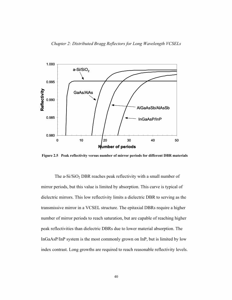
Figure 2.5 Peak reflectivity versus number of mirror periods for different DBR materials
00
The a-Si/SiO2 DBR reaches peak reflectivity with a small number of
mirror periods, but this value is limited by absorption. This curve is typical of
dielectric mirrors. This low reflectivity limits a dielectric DBR to serving as the
transmissive mirror in a VCSEL structure. The epitaxial DBRs require a higher
number of mirror periods to reach saturation, but are capable of reaching higher
peak reflectivities than dielectric DBRs due to lower material absorption. The
InGaAsP/InP system is the most commonly grown on InP, but is limited by low
index contrast. Long growths are required to reach reasonable reflectivity levels.
40
Chapter 2: Distributed Bragg Reflectors for Long Wavelength VCSELs
The same is true of AlInGaAs/AlInAs DBRs, not shown in the figure. The
AlGaAsSb/AlAsSb system has been studied extensively for DBR applications on
InP[4, 53]. This system features significantly higher index contrast than other
epitaxial mirrors grown on InP. GaAs/AlAs DBRs have slightly higher index
contrast than Sb-based DBRs, requiring fewer periods to reach a given
reflectivity.
2.3.2. Optical Bandwidth
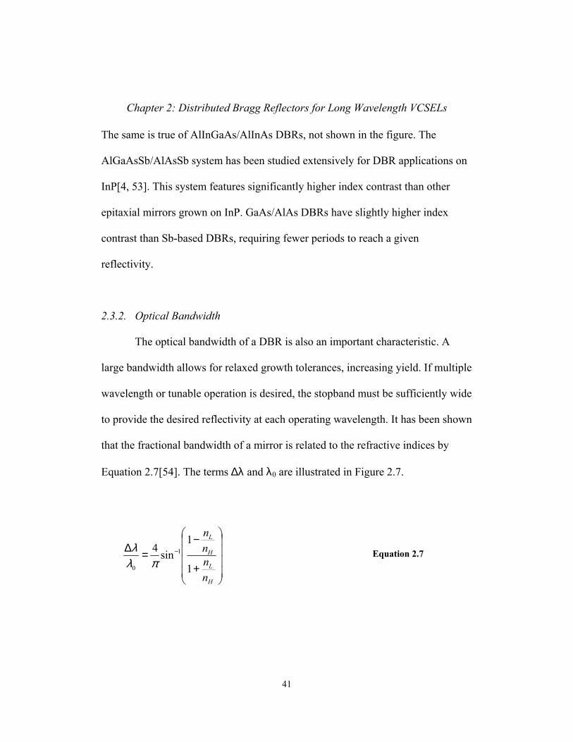
The optical bandwidth of a DBR is also an important characteristic. A
large bandwidth allows for relaxed growth tolerances, increasing yield. If multiple
wavelength or tunable operation is desired, the stopband must be sufficiently wide
to provide the desired reflectivity at each operating wavelength. It has been shown
that the fractional bandwidth of a mirror is related to the refractive indices by
Equation 2.7[54]. The terms ∆λ and λ0 are illustrated in Figure 2.7.
+
−=∆ −
H
L
H
L
nnnn
1
1sin4 1
0 πλλ Equation 2.7
41

Chapter 2: Distributed Bragg Reflectors for Long Wavelength VCSELs
0
0.1
0.2
0.3
0.4
0.5
0.6
0.7
0.8
0.9
1
1300 1400 1500 1600 1700 1800
Wavelength (nm)
Ref
lect
ivity
∆λ
λ0
0
0.1
0.2
0.3
0.4
0.5
0.6
0.7
0.8
0.9
1
1300 1400 1500 1600 1700 1800
Wavelength (nm)
Ref
lect
ivity
∆λ
λ0
Figure 2.7 Bandwidth and center wavelength of DBR
λ0 is the center wavelength of the DBR. It should be noted that that ∆λ is
the full width at half maximum (FWHM) of the DBR stopband. Although the
reflectivity is no longer high enough to support lasing near the FWHM endpoints,
the fractional bandwidth is still a useful qualitative figure of merit for comparing
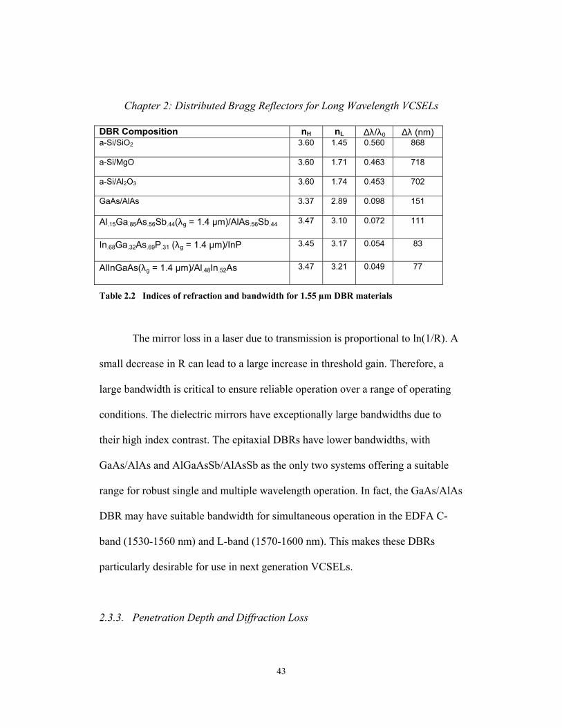
different DBR media. Table 2.2 shows indices of refraction, fractional bandwidth
and bandwidth for common 1.55 µm DBR materials.
42
Chapter 2: Distributed Bragg Reflectors for Long Wavelength VCSELs
DBR Composition nH nL ∆λ/λ0 ∆λ (nm) a-Si/SiO2 3.60 1.45 0.560 868
a-Si/MgO 3.60 1.71 0.463 718
a-Si/Al2O3 3.60 1.74 0.453 702
GaAs/AlAs 3.37 2.89 0.098 151
Al.15Ga.85As.56Sb.44(λg = 1.4 µm)/AlAs.56Sb.44 3.47 3.10 0.072 111
In.68Ga.32As.69P.31 (λg = 1.4 µm)/InP 3.45 3.17 0.054 83
AlInGaAs(λg = 1.4 µm)/Al.48In.52As 3.47 3.21 0.049 77
Table 2.2 Indices of refraction and bandwidth for 1.55 µm DBR materials
The mirror loss in a laser due to transmission is proportional to ln(1/R). A
small decrease in R can lead to a large increase in threshold gain. Therefore, a
large bandwidth is critical to ensure reliable operation over a range of operating
conditions. The dielectric mirrors have exceptionally large bandwidths due to
their high index contrast. The epitaxial DBRs have lower bandwidths, with
GaAs/AlAs and AlGaAsSb/AlAsSb as the only two systems offering a suitable
range for robust single and multiple wavelength operation. In fact, the GaAs/AlAs
DBR may have suitable bandwidth for simultaneous operation in the EDFA C-
band (1530-1560 nm) and L-band (1570-1600 nm). This makes these DBRs
particularly desirable for use in next generation VCSELs.
2.3.3. Penetration Depth and Diffraction Loss
43
Chapter 2: Distributed Bragg Reflectors for Long Wavelength VCSELs
The effective penetration depth of the optical field into the DBR is
approximated by λ/4∆n, where ∆n = nH - nL[43]. It is apparent that high index
contrast reduces the effective penetration depth of the optical field into the DBR.
This results in reduced material and free carrier absorption. The calculations
above assume incident plane waves and neglect diffraction loss. The effects of
diffraction loss have been calculated previously[55]. Diffraction loss increases
with the penetration depth. Recent devices feature lateral index guiding for mode
confinement, reducing diffraction and scattering losses. This index guiding may
be achieved through regrowth, or more commonly with a lateral dielectric
aperture. The lateral oxidation of AlGaAs alloys has enabled the fabrication of
short wavelength VCSELs with low optical loss[56]. This aperture may also be
used to provide current confinement. At this time, a similarly robust aperturing
technology on InP is not available, although efforts have been made in selective
lateral etching and in the oxidation of Al containing compounds[57, 58].
2.3.4. Summary
44

Chapter 2: Distributed Bragg Reflectors for Long Wavelength VCSELs
Dielectric DBRs offer reasonably high reflectivities for output mirrors
with a short number of mirror periods. However, these DBRs are not sufficiently
reflective to serve as the non-transmissive mirror and are difficult to integrate as a
bottom mirror in a practical device. Mechanical reliability is also a concern.
Traditional epitaxial DBRs on InP are plagued by low index contrast and require
arduously long growths to reach desired reflectivity levels. These thick mirrors
lead to increased diffraction losses. The recent use of AlGaAsSb as a mirror
material has improved optical performance. However, it will be shown that DBRs
based on ternary and quaternary alloys have poor thermal conductivity, limiting
the prospects for high temperature operation. GaAs/AlAs DBRs may be used as
either the transmissive or reflective mirror in a VCSEL, depending on the number
of periods. These DBRs offer high reflectivity with reduced thickness compared
to DBRs grown on InP. In addition to these favorable longitudinal optical
characteristics, the lateral oxidation of AlGaAs compounds may be used to
provide transverse optical confinement, further reducing diffraction losses. This
aperture may also be used for current confinement. GaAs/AlAs DBRs have
sufficient optical bandwidth to support single and multiple channel operation over
a wide temperature range.
2.4. Thermal Properties
45

Chapter 2: Distributed Bragg Reflectors for Long Wavelength VCSELs
The thermal properties of DBRs are of paramount importance. The DBRs
comprise the bulk of the VCSEL and must be able to effectively dissipate heat
from resistive and lasing processes. This is particularly crucial for long
wavelength VCSELs, due to the low characteristic temperature of InP active
regions. Dielectric mirrors typically exhibit low thermal conductivities, though
materials such as MgO and Al2O3 have been introduced with improved
results[21]. The thermal conductivity of epitaxially grown DBRs depends greatly
on alloy composition. Ternary and quaternary alloys generally have lower thermal
conductivities than binary mirrors, due to alloy scattering[59].
To dissipate heat from the active layer, heat flow must occur through or
around the DBRs. Thermal conductance in the radial and longitudinal directions
may be calculated knowing the thicknesses and thermal conductivities of the
constituent material. It is appropriate to consider radial coordinates due to the
cylindrical symmetry of most VCSELs. The following analysis was used by
Dudley[60]. Consider a periodic combination of two different material with
thicknesses d1 and d2, and thermal conductivities κ1 and κ2 as shown in Figure 2.8.
46

Chapter 2: Distributed Bragg Reflectors for Long Wavelength VCSELs
κz
longitudinal
κr, radial
κ2, d2
κ1, d1
κ2, d2
κ1, d1
κ2, d2
κ1, d1
κz
longitudinal
κr, radial
κ2, d2
κ1, d1
κ2, d2
κ1, d1
κ2, d2
κ1, d1
Figure 2.8 Radial and longitudinal thermal conductivity in a DBR
The radial and longitudinal thermal conductivities are given by
Equation 2.8 21
2211
dddd
r ++= κκκ
Equation 2.9 1221
2121 )(dddd
z κκκκκ
++=
These expressions can be simplified further by considering the optical
properties of the DBR. The thickness of each layer, di, is given by di = λi/4ni,
where ni is the refractive index of the layer. Making this substitution, the thermal
47

Chapter 2: Distributed Bragg Reflectors for Long Wavelength VCSELs
conductivities in each direction can be written in terms of the refractive indices
and the thermal conductivities of each layer.
Equation 2.10 21
1221
nnnn
r ++= κκκ
Equation 2.11 2211
2121 )(nnnn
z κκκκκ
++=
The average thermal conductivity for both directions can be calculated by
taking the geometric mean of the radial and longitudinal thermal conductivities.
Equation 2.12 )( 212211
1221 κκκκκκκκκ
nnnn
zravg ++==
The thermal resistance of a DBR depends on the device geometry and any
additional materials in the structure. Thermal conductivities in DBRs are
significantly reduced from the expected bulk material values by phonon
scattering, since the distance between material interfaces is on the order of a mean
free phonon length. However, the approximations given above are useful for
comparing the relative thermal merits of different DBRs based on their intrinsic
material properties. Table 2.3 lists the individual, radial and longitudinal thermal
48

Chapter 2: Distributed Bragg Reflectors for Long Wavelength VCSELs
conductivities for different DBR materials[47, 59, 61]. The first material listed is
referred to with the subscript 1.
DBR Composition κ1 (W/cm K)
κ2 (W/cm K)
κr (W/cm K)
κz (W/cm K)
κavg (W/cm K)
a-Si/SiO2 0.026 0.012 0.016 0.014 0.015
a-Si/MgO 0.026 0.53 0.368 0.073 0.164
a-Si/Al2O3 0.026 0.36 0.251 0.069 0.132
GaAs/AlAs 0.44 0.91 0.693 0.609 0.650
Al.15Ga.85As.56Sb.44/AlAs.56Sb.44 0.062 0.057 0.059 0.059 0.059
In.68Ga.32As.69P.31/InP 0.045 0.68 0.376 0.088 0.182
AlInGaAs/Al.48In.52As 0.045 0.045 0.045 0.045 0.045
Table 2.3 Individual, directional and average thermal conductivities for DBR materials
It should be noted that the thermal conductivity for a-Si is far lower than
that of crystalline silicon. The poor thermal conductivity of traditional dielectric
mirrors such as a-Si/SiO2 is apparent. Improved dielectric designs have thermal
conductivities similar to that of InGaAsP. The a-Si/SiO2 , AlGaAsSb/AlAsSb and
AlInGaAs/AlInAs combinations behave as thermal insulators. Epitaxial DBRs
fabricated using ternary and quaternary alloys generally have low thermal
conductivities compared to the binary GaAs/AlAs mirrors. Most of the DBRs that
do conduct heat will behave as heat spreaders, since κr >>κz. Only GaAs/AlAs
DBRs allow effective heat transport through the mirror.
49

Chapter 2: Distributed Bragg Reflectors for Long Wavelength VCSELs
In practice, AlxGa1-xAs alloys are used in the formation of DBRs, typically
with x ≥ 0.9. This allows the selective oxidation of alloys with x ≥ 0.98. Despite
increased alloy scattering in the ternary, AlxGa1-xAs maintains a high thermal
conductivity over the range of interest, illustrated in Figure 2.9 [62].
κ(W
/cm
K)
0.00
0.10
0.20
0.30
0.40
0.50
0.60
0.70
0.80
0.90
1.00
0 0.1 0.2 0.3 0.4 0.5 0.6 0.7 0.8 0.9 1
x (Al fraction)
AlxGa1-xAs
κ(W
/cm
K)
0.00
0.10
0.20
0.30
0.40
0.50
0.60
0.70
0.80
0.90
1.00
0 0.1 0.2 0.3 0.4 0.5 0.6 0.7 0.8 0.9 1
x (Al fraction)
AlxGa1-xAs
Figure 2.9 Thermal conductivity of AlxGa1-xAs
2.5. Electrical Properties
Current supply through semiconductor DBRs is the simplest and most
uniform way to inject carriers into the VCSEL active region. However, doping
50
Chapter 2: Distributed Bragg Reflectors for Long Wavelength VCSELs
semiconductor mirrors for current transport also increases optical loss, limiting
peak reflectivity. A balance must be struck between high reflectivity and low
electrical resistance. The voltage across a DBR is determined by the resistance of
each mirror period and the potential difference across each of the large number of
heterobarriers. The resistance of p-type DBRs is much greater than that of
comparable n-type DBRs, due to lower hole mobility and large valence band
offsets. In this section, the electrical characteristics of p-GaAs/AlGaAs DBRs are
explored. The optical and thermal properties of these DBRs presented in earlier
sections indicate their suitability for 1.55 µm VCSELs. Design of p-type DBRs is
a greater challenge than n-type due to higher resistance and increased free carrier
absorption. The impact of electrical design improvements on optical properties is
discussed. One-dimensional simulations of current transport are used to compare
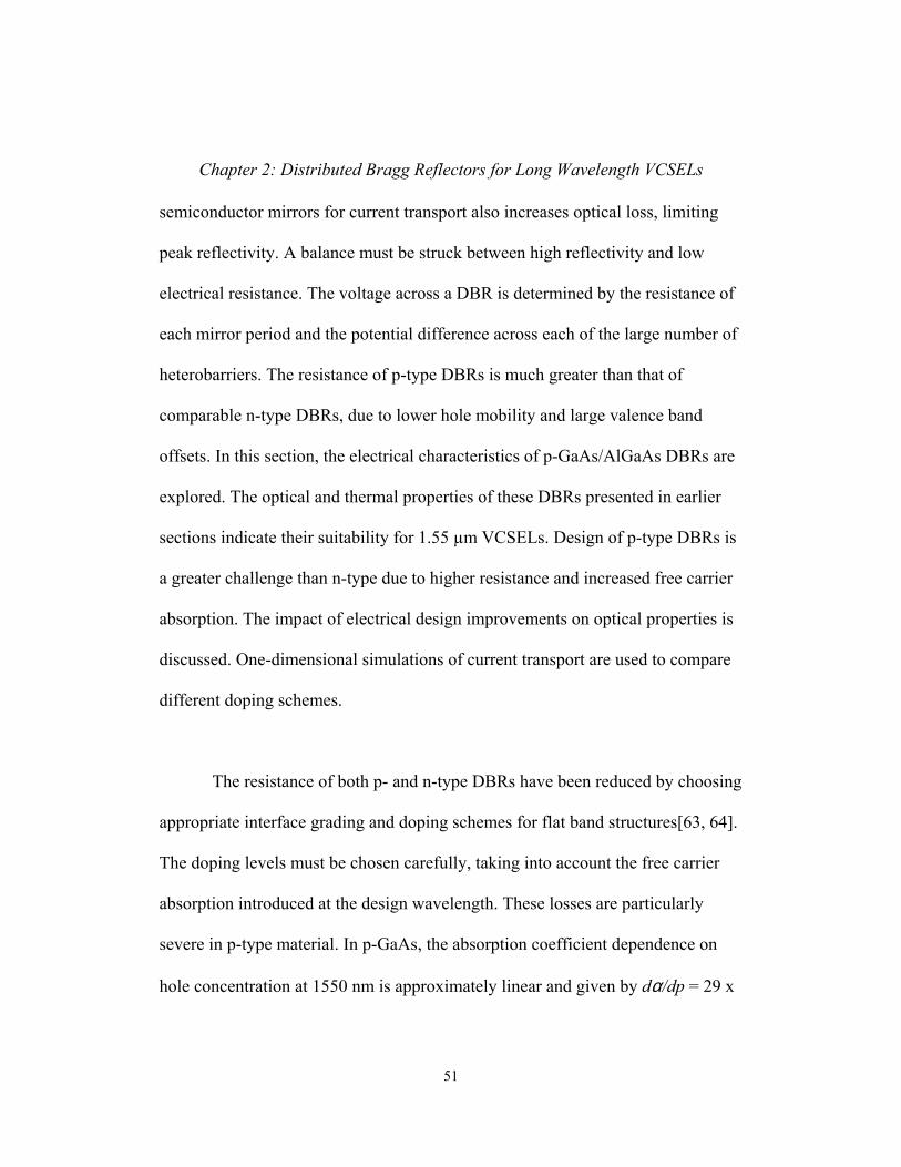
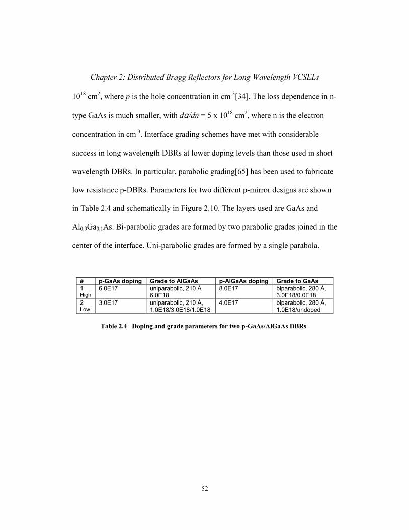
different doping schemes.
The resistance of both p- and n-type DBRs have been reduced by choosing
appropriate interface grading and doping schemes for flat band structures[63, 64].
The doping levels must be chosen carefully, taking into account the free carrier
absorption introduced at the design wavelength. These losses are particularly
severe in p-type material. In p-GaAs, the absorption coefficient dependence on
hole concentration at 1550 nm is approximately linear and given by dα/dp = 29 x
51
Chapter 2: Distributed Bragg Reflectors for Long Wavelength VCSELs
1018 cm2, where p is the hole concentration in cm-3[34]. The loss dependence in n-
type GaAs is much smaller, with dα/dn = 5 x 1018 cm2, where n is the electron
concentration in cm-3. Interface grading schemes have met with considerable
success in long wavelength DBRs at lower doping levels than those used in short
wavelength DBRs. In particular, parabolic grading[65] has been used to fabricate
low resistance p-DBRs. Parameters for two different p-mirror designs are shown
in Table 2.4 and schematically in Figure 2.10. The layers used are GaAs and
Al0.9Ga0.1As. Bi-parabolic grades are formed by two parabolic grades joined in the
center of the interface. Uni-parabolic grades are formed by a single parabola.
# p-GaAs doping Grade to AlGaAs p-AlGaAs doping Grade to GaAs 1 High
6.0E17 uniparabolic, 210 Å 6.0E18
8.0E17 biparabolic, 280 Å, 3.0E18/0.0E18
2 Low
3.0E17 uniparabolic, 210 Å, 1.0E18/3.0E18/1.0E18
4.0E17 biparabolic, 280 Å, 1.0E18/undoped
Table 2.4 Doping and grade parameters for two p-GaAs/AlGaAs DBRs
52

Chapter 2: Distributed Bragg Reflectors for Long Wavelength VCSELs
53
Position (µm)0 0.05 0.10 0.15 0.20 0.25
0
0.2
0.4
0.6
0.8
1.0
Al f
ract
ion N
a (cm-3)
0
2
4
6
8
10
Na (cm-3)
Al fraction#1, high doping
Position (µm)0 0.05 0.10 0.15 0.20 0.25
0
0.2
0.4
0.6
0.8
1.0
Al f
ract
ion N
a (cm-3)
0
2
4
6
8
10
Na (cm-3)
Al fraction#1, high doping
Position (µm)0 0.05 0.10 0.15 0.20 0.25
0
0.2
0.4
0.6
0.8
1.0
Al f
ract
ion N
a (cm-3)
0
2
4
6
8
10
Na (cm-3)
Al fraction#2, low doping
Position (µm)0 0.05 0.10 0.15 0.20 0.25
0
0.2
0.4
0.6
0.8
1.0
Al f
ract
ion N
a (cm-3)
0
2
4
6
8
10
Na (cm-3)
Al fraction#2, low doping
Figure 2.10 Composition and doping profile of graded p-DBRs
Chapter 2: Distributed Bragg Reflectors for Long Wavelength VCSELs
The first design features higher doping in the periods and at the
GaAs/AlGaAs interfaces. A common feature to both designs is increased doping
in AlGaAs relative to GaAs. This is intended to compensate for the reduced hole
mobility in AlGaAs compared to GaAs. The interface doping is higher at the
transition from GaAs to AlGaAs. This portion of the DBR is located at a null in
the cavity standing wave. As a result, doping can be increased without incurring
excessive loss. Cavity design and standing wave patterns will be explored more
thoroughly in Chapter 4. Results from a one-dimensional current transport
simulation[66] are shown in Figure 2.11 for a 23 period DBR of each type.
0
10
20
30
40
50
60
70
80
90
100
0 1 2 3 4 5
Voltage (V)
Cur
rent
Den
sity
(kA
/cm
2 )
High doping
Low doping
0
10
20
30
40
50
60
70
80
90
100
0 1 2 3 4 5
Voltage (V)
Cur
rent
Den
sity
(kA
/cm
2 )
High doping
Low doping
Figure 2.11 Voltage-current density characteristic for high and low doping designs
54

Chapter 2: Distributed Bragg Reflectors for Long Wavelength VCSELs
As expected, the second mirror is far more resistive. The highly doped
mirror passes 18 kA/cm2 at 1 V and the low doped mirror passes 6 kA/cm2 at 1 V.
The eventual design used for portions of this dissertation used 15 highly doped
periods far from the active region (where the standing wave intensity is weak) and
8 lowly doped periods close to the active region (where the standing wave
intensity is higher). This combination was used to reduce the loss-resistance
product, which is an appropriate figure of merit for a conducting mirror. A more
complete description of mirror interface grading and the loss-resistance product
may be found in work by Hegblom[67]. The cavity and mirror design will be
examined more thoroughly in Chapter 4. A 23 period mirror consisting of 15
highly doped and 8 lowly doped periods will pass approximately 10 kA/cm2 with
a potential drop of 1 V. This current density far exceeds the threshold current
density required in long wavelength VCSELs, which is typically on the order of
1-4 kA/cm2, depending on device size. Although a p-DBR is more resistive than
an n-DBR, it is apparent that this p-GaAs/AlGaAs DBR is suitable for VCSEL
current injection. It is important to minimize the resistive contribution of the DBR
to reduce device self-heating and increase intrinsic bandwidth.
It remains to be seen what the optical properties of this graded, doped
DBR will be. Factor p from Equation 2.1 must be modified to consider non-abrupt
55

Chapter 2: Distributed Bragg Reflectors for Long Wavelength VCSELs
interfaces. The change in factor p at the DBR center wavelength for a graded
DBR is determined by the following expression[45]:
f
H
L
nnp
= Equation 2.13
where f is the ratio of the fundamental Fourier series coefficient of the index
profile with grading to that without grading. The reflectivity spectrum can be
calculated using the 1-D transfer matrix method, with standing wave effects
considered to calculate the loss contributions at different points in the DBR[43,
68]. Combining electrical and optical calculations, the following result is
obtained, where R, T and L denote power reflection, transmission and loss,
respectively.
DBR # of periods Resistance (Ω µm2) R (%) T (%) L (%)
p-GaAs/Al0.9Ga0.1 As 23 9470 99.39 0.27 0.34
Table 2.5 Summary of calculated p-GaAs/Al0.9Ga0.1As DBR properties
The calculated resistance should be divided by the device area to
determine the actual resistance. These results indicate a good balance between
electrical and optical properties. The reflectivity is appropriate for a 1.55 VCSEL
56

Chapter 2: Distributed Bragg Reflectors for Long Wavelength VCSELs
output DBR. The reflective DBR will either be n-doped or undoped in the case of
an intracavity contact. In general, higher resistance and optical loss make design
of the p-DBR a greater challenge than design of undoped or n-DBRs. A detailed
analysis of gain and loss in the optical cavity will be presented in Chapter 4. For a
device with a cross-sectional area of 1000 µm2 (diameter = 36 µm), the expected
resistance of the p-DBR is less than 10 Ω. The measured mirror resistance for this
diameter is 19 Ω, in reasonable agreement with a 1-D calculation. The
discrepancy may be attributed to the high lateral mobility in structures grown
using carbon as a p-dopant. The low resistance indicates that the mirror will not
be a significant contributor to device self-heating and that it is suitable for use in a
high-speed structure.
2.6. Summary
In this chapter, the optical and thermal properties of 1.55 µm VCSEL
DBRs were considered. The GaAs/AlGaAs system was shown to have suitable
qualities, including high reflectivity, high thermal conductivity and low electrical
resistance. These DBRs can serve as a transmissive or reflective VCSEL mirror.
An oxide aperture may be introduced for lateral index guiding. GaAs/AlGaAs
mirrors have been shown to provide the most effective path for heat dissipation
among long wavelength DBRs. The electrical characteristics of doped, graded p-
57
Chapter 2: Distributed Bragg Reflectors for Long Wavelength VCSELs
GaAs/AlGaAs DBRs were found to be suitable for high-speed, low power
operation. Effective current transport may be achieved without compromising the
optical properties of the DBR. The reliability and robust fabrication of these
mirrors have been demonstrated in commercial short wavelength devices. The
next chapter discusses the concept of wafer bonding as a method for integrating
GaAs/AlGaAs DBRs with InP-based active regions.
References
[1] F. Salomonsson, S. Mogg, S. Rapp, J. Bentell, I. Sagnes, R. Raj, K.
Streubel, and M. Hammar, "Temperature-dependent performance of 1.55
µm vertical-cavity lasers with InGaAsP/InP bottom mirror," Proceedings
of Eleventh International Conference on Indium Phosphide and Related
Materials, pp. 223-6, 1999.
[2] P. Salet, P. Pagnod-Rossiaux, F. Gaborit, A. Plais, and J. Jacquet, "Gas-
source molecular-beam epitaxy and optical characterisation of highly-
reflective InGaAsP/InP multilayer Bragg mirrors for 1.3 µm vertical-
cavity lasers," Electronics Letters, vol. 33, pp. 1145-7, 1997.
[3] J. K. Kim, S. Nakagawa, E. Hall, and L. A. Coldren, "Near-room-
temperature continuous-wave operation of multiple-active-region 1.55 µm
58
Chapter 2: Distributed Bragg Reflectors for Long Wavelength VCSELs
vertical-cavity lasers with high differential efficiency," Applied Physics
Letters, vol. 77, pp. 3137-9, 2000.
[4] O. Blum, M. J. Hafich, J. F. Klem, K. L. Lear, and S. N. G. Chu,
"Electrical and optical characteristics of AlAsSb/GaAsSb distributed
Bragg reflectors for surface emitting lasers," Applied Physics Letters, vol.
67, pp. 3233-5, 1995.
[5] G. Almuneau, E. Hall, S. Nakagawa, J. K. Kim, D. Lofgreen, O. Sjolund,
C. Luo, D. R. Clarke, J. H. English, and L. A. Coldren, "Molecular beam
epitaxial growth of monolithic 1.55 µm vertical cavity surface emitting
lasers with AlGaAsSb/AlAsSb Bragg mirrors," Journal of Vacuum
Science & Technology B, vol. 18, pp. 1601-4, 2000.
[6] E. Hall, G. Almuneau, J. K. Kim, O. Sjolund, H. Kroemer, and L. A.
Coldren, "Electrically-pumped, single-epitaxial VCSELs at 1.55 µm with
Sb-based mirrors," Electronics Letters, vol. 35, pp. 1337-8, 1999.
[7] L. Goldstein, C. Fortin, C. Starck, A. Plais, J. Jacquet, J. Boucart, A.
Rocher, and C. Poussou, "GaAlAs/GaAs metamorphic Bragg mirror for
long wavelength VCSELs," Electronics Letters, vol. 34, pp. 268-70, 1998.
[8] J. Boucart, C. Starck, F. Gaborit, A. Plais, N. Bouche, E. Derouin, J. C.
Remy, J. Bonnet-Gamard, L. Goldstein, C. Fortin, D. Carpentier, P. Salet,
F. Brillouet, and J. Jacquet, "Metamorphic DBR and tunnel-junction
59
Chapter 2: Distributed Bragg Reflectors for Long Wavelength VCSELs
injection. A CW RT monolithic long-wavelength VCSEL," IEEE Journal
of Selected Topics in Quantum Electronics, vol.5, pp. 520-9, 1999.
[9] H. Shoji, K. Otsubo, T. Fujii, and H. Ishikawa, "Calculated performances
of 1.3-µm vertical-cavity surface-emitting lasers on InGaAs ternary
substrates," IEEE Journal of Quantum Electronics, vol. 33, pp. 238-45,
1997.
[10] F. E. Ejeckam, Y. H. Lo, S. Subramanian, H. Q. Hou, and B. E.
Hammons, "Lattice engineered compliant substrate for defect-free
heteroepitaxial growth," Applied Physics Letters, vol. 70, pp. 1685-7,
1997.
[11] W. A. Jesser, J. H. van der Merwe, and P. M. Stoop, "Misfit
accommodation by compliant substrates," Journal of Applied Physics, vol.
85, pp. 2129-39, 1999.
[12] K. D. Choquette, J. F. Klem, A. J. Fischer, O. Blum, A. A. Allerman, I. J.
Fritz, S. R. Kurtz, W. G. Breiland, R. Sieg, K. M. Geib, J. W. Scott, and R.
L. Naone, "Room temperature continuous wave InGaAsN quantum well
vertical cavity lasers emitting at 1.3 µm," Electronics Letters, vol. 36, pp.
1388-1390, 2000.
[13] M. C. Larson, C. W. Coldren, S. G. Spruytte, H. E. Petersen, and J. S.
Harris, "Low-threshold oxide-confined GaInNAs long wavelength vertical
60
Chapter 2: Distributed Bragg Reflectors for Long Wavelength VCSELs
cavity lasers," IEEE Photonics Technology Letters, vol. 12, pp. 1598-600,
2000.
[14] J. A. Lott, N. N. Ledentsov, V. M. Ustinov, N. A. Maleev, A. E. Zhukov,
A. R. Kovsh, M. V. Maximov, B. V. Volovik, Z. I. Alferov, and D.
Bimberg, "InAs-InGaAs quantum dot VCSELs on GaAs substrates
emitting at 1.3 µm," Electronics Letters, vol. 36, pp. 1384-5, 2000.
[15] J. A. Lott, N. N. Ledentsov, V. M. Ustinov, N. A. Maleev, A. E. Zhukov,
M. V. Maximov, B. V. Volovik, Z. I. Alferov, and D. Bimberg, "Vertical
cavity surface emitting lasers with InAs-InGaAs quantum dot active
regions on GaAs substrates emitting at 1.3 µm," Conference Digest IEEE
17th International Semiconductor Laser Conference, pp. 13-14, 2000.
[16] H. Soda, K. Iga, C. Kitahara, and Y. Suematsu, "GaInAsP/InP surface
emitting injection lasers," Japanese Journal of Applied Physics, vol. 18,
pp. 2329-30, 1979.
[17] H. Wada, D. I. Babic, D. L. Crawford, T. E. Reynolds, J. J. Dudley, J. E.
Bowers, E. L. Hu, J. L. Merz, B. I. Miller, U. Koren, and M. G. Young,
"Low-threshold, high-temperature pulsed operation of InGaAsP/InP
vertical cavity surface emitting lasers," IEEE Photonics Technology
Letters, vol. 3, pp. 977-9, 1991.
61

Chapter 2: Distributed Bragg Reflectors for Long Wavelength VCSELs
[18] T. Tadokoro, H. Okamoto, Y. Kohama, T. Kawakami, and T. Kurokawa,
"Room temperature pulsed operation of 1.5 µm GaInAsP/InP vertical-
cavity surface-emitting laser," IEEE Photonics Technology Letters, vol. 4,
pp. 409-11, 1992.
[19] M. Ortsiefer, R. Shau, G. Bohm, F. Kohler, and M. C. Amann, "Low-
threshold index-guided 1.5 µm long-wavelength vertical-cavity surface-
emitting laser with high efficiency," Applied Physics Letters, vol. 76, pp.
2179-81, 2000.
[20] G. Stern, "Band-tail model for optical absorption and for the mobility edge
in amorphous silicon," Physical Review B (Solid State), vol. 3, pp. 2636-
45, 1971.
[21] S. Uchiyama, N. Yokouchi, and T. Ninomiya, "Continuous-wave
operation up to 36 degrees C of 1.3-µm GaInAsP-InP vertical-cavity
surface-emitting lasers," IEEE Photonics Technology Letters, vol. 9, pp.
141-2, 1997.
[22] T. Baba, Y. Yogo, K. Suzuki, F. Koyama, and K. Iga, "Near room
temperature continuous wave lasing characteristics of GaInAsP/InP
surface emitting laser," Electronics Letters, vol. 29, pp. 913-14, 1993.
62

Chapter 2: Distributed Bragg Reflectors for Long Wavelength VCSELs
[23] H. Wada, D. I. Babic, M. Ishikawa, and J. E. Bowers, "Effects of
nonuniform current injection in GaInAsP/InP vertical-cavity lasers,"
Applied Physics Letters, vol. 60, pp. 2974-6, 1992.
[24] W. Nakwaski and M. Osinski, "Thermal properties of etched-well surface-
emitting semiconductor lasers," IEEE Journal of Quantum Electronics,
vol. 27, pp. 1391-401, 1991.
[25] M. Ortsiefer, R. Shau, M. Zigldrum, G. Bohm, F. Kohler, and M. C.
Amann, "Submilliamp long-wavelength InP-based vertical-cavity surface-
emitting laser with stable linear polarisation," Electronics Letters, vol. 36,
pp. 1124-6, 2000.
[26] J. J. Dudley, M. Ishikawa, D. I. Babic, B. I. Miller, R. Mirin, W. B. Jiang,
J. E. Bowers, and E. L. Hu, "144°C operation of 1.3 µm InGaAsP vertical
cavity lasers on GaAs substrates," Applied Physics Letters, vol. 61, pp.
3095-7, 1992.
[27] J. J. Dudley, D. I. Babic, R. Mirin, L. Yang, B. I. Miller, R. J. Ram, T.
Reynolds, E. L. Hu, and J. E. Bowers, "Low threshold, wafer fused long
wavelength vertical cavity lasers," Applied Physics Letters, vol. 64, pp.
1463-5, 1994.
63

Chapter 2: Distributed Bragg Reflectors for Long Wavelength VCSELs
[28] Y. H. Lo, R. Bhat, D. M. Hwang, M. A. Koza, and T. P. Lee, "Bonding by
atomic rearrangement of InP/InGaAsP 1.5 µm wavelength lasers on GaAs
substrates," Applied Physics Letters, vol. 58, pp. 1961-3, 1991.
[29] H. Wada, Y. Ogawa, and T. Kamijoh, "Electrical characteristics of
directly-bonded GaAs and InP," Applied Physics Letters, vol. 62, pp. 738-
40, 1993.
[30] N. Y. Jin-Phillipp, W. Sigle, A. Black, D. Babic, J. Bowers, E. L. Hu, and
M. Ruhle, "Interface of directly bonded GaAs and InP," Journal of
Applied Physics, vol. 89, pp. 1017-1024, 2001.
[31] S. Rapp, F. Salomonsson, J. Bentell, I. Sagnes, H. Moussa, C. Meriadec,
R. Raj, K. Streubel, and M. Hammar, "Near room-temperature continuous-
wave operation of electrically pumped 1.55 µm vertical cavity lasers with
InGaAsP/InP bottom mirror," Electronics Letters, vol. 35, pp. 49-50,
1999.
[32] Y. Qian, Z. H. Zhu, Y. H. Lo, D. L. Huffaker, D. G. Deppe, H. Q. Hou, B.
E. Hammons, W. Lin, and Y. K. Tu, "Low-threshold proton-implanted
1.3-µm vertical-cavity top-surface-emitting lasers with dielectric and
wafer-bonded GaAs-AlAs Bragg mirrors," IEEE Photonics Technology
Letters, vol. 9, pp. 866-8, 1997.
64
Chapter 2: Distributed Bragg Reflectors for Long Wavelength VCSELs
[33] N. M. Margalit, J. Piprek, S. Zhang, D. I. Babic, K. Streubel, R. P. Mirin,
J. R. Wesselmann, and J. E. Bowers, "64°C continuous-wave operation of
1.5-µm vertical-cavity laser," IEEE Journal of Selected Topics in
Quantum Electronics, vol. 3, pp. 359-65, 1997.
[34] D. I. Babic, J. Piprek, K. Streubel, R. P. Mirin, N. M. Margalit, D. E.
Mars, J. E. Bowers, and E. L. Hu, "Design and analysis of double-fused
1.55-µm vertical-cavity lasers," IEEE Journal of Quantum Electronics,
vol. 33, pp. 1369-83, 1997.
[35] K. A. Black, P. Abraham, N. M. Margalit, E. R. Hegblom, Y. J. Chiu, J.
Piprek, J. E. Bowers, and E. L. Hu, "Double-fused 1.5 µm vertical cavity
lasers with record high T0 of 132 K at room temperature," Electronics
Letters, vol. 34, pp. 1947-9, 1998.
[36] A. Karim, P. Abraham, D. Lofgreen, Y. J. Chiu, J. Piprek, and J. E.
Bowers, "Wafer bonded 1.55 µm vertical cavity lasers with continuous
wave operation up to 105°C," Appl. Phys. Lett., 2001.
[37] V. Jayaraman, J. C. Geske, M. MacDougal, F. Peters, T. Lowes, T. Char,
D. Van Deusen, T. Goodnough, M. Donhowe, S. Kilcoyne, and D. Welch,
"Long-wavelength vertical-cavity laser research at Gore," Proceedings of
the SPIE, vol. 3627, pp. 29-37, 1999.
65

Chapter 2: Distributed Bragg Reflectors for Long Wavelength VCSELs
[38] I. H. Tan, D. A. Vanderwater, J. W. Huang, G. E. Hofler, F. A. Kish, E. I.
Chen, and T. D. Ostentowski, "Wafer bonding of 75 mm diameter GaP to
AlGaInP-GaP light-emitting diode wafers," Journal of Electronic
Materials, vol. 29, pp. 188-94, 2000.
[39] E. S. Björlin, B. Riou, A. Keating, P. Abraham, Y. J. Chiu, J. Piprek, and
J. E. Bowers, "1.3 µm vertical cavity amplifier," IEEE Photonics
Technology Letters, vol. 12, 2000.
[40] Y. Xiong, Y. Zhou, Z. H. Zhu, Y. H. Lo, C. Ji, S. A. Basher, A. A.
Allerman, T. Hargett, R. Sieg, and K. D. Choquette, "Oxide-defined GaAs
vertical-cavity surface-emitting lasers on Si substrates," IEEE Photonics
Technology Letters, vol. 12, pp. 110-12, 2000.
[41] A. R. Hawkins, W. Weishu, P. Abraham, K. Streubel, and J. E. Bowers,
"High gain-bandwidth-product silicon heterointerface photodetector,"
Applied Physics Letters, vol. 70, pp. 303-5, 1997.
[42] B. F. Levine, A. R. Hawkins, S. Hiu, B. J. Tseng, C. A. King, L. A.
Gruezke, R. W. Johnson, D. R. Zolnowski, and J. E. Bowers, "20 GHz
high performance planar Si/InGaAs p-i-n photodetector," Applied Physics
Letters, vol. 70, pp. 2449-51, 1997.
[43] L. A. Coldren and S. Corzine, Diode Lasers and Photonic Integrated
Circuits. New York, NY: John Wiley & Sons, Inc., 1995.
66

Chapter 2: Distributed Bragg Reflectors for Long Wavelength VCSELs
[44] D. I. Babic, "Double-fused long-wavelength vertical-cavity lasers," in
Electrical and Computer Engineering. Santa Barbara, CA: University of
California, Santa Barbara, 1995.
[45] S. W. Corzine, R. H. Yan, and L. A. Coldren, "A tanh substitution
technique for the analysis of abrupt and graded interface multilayer
dielectric stacks," IEEE Journal of Quantum Electronics, vol. 27, pp.
2086-90, 1991.
[46] D. I. Babic and S. W. Corzine, "Analytic expressions for the reflection
delay, penetration depth, and absorptance of quarter-wave dielectric
mirrors," IEEE Journal of Quantum Electronics, vol. 28, pp. 514-24,
1992.
[47] D. Babic, J. Piprek, and J. Bowers, "Long-Wavelength Vertical Cavity
Lasers," in Vertical-Cavity Surface-Emitting Lasers, C. Wilmsen, H.
Temkin, and L. A. Coldren, Eds. Cambridge, UK: Cambridge University
Press, 1999, pp. 303-333.
[48] M. A. Afromovitz, "Refractive index of Ga1-xAlxAs," Solid State
Communications, vol. 15, pp. 59-63, 1974.
[49] S. Adachi, "Refractive indices of III-V compounds: key properties of
InGaAsP relevant to device design," Journal of Applied Physics, vol. 53,
pp. 5863-9, 1982.
67

Chapter 2: Distributed Bragg Reflectors for Long Wavelength VCSELs
[50] M. J. Mondry, D. I. Babic, J. E. Bowers, and L. A. Coldren, "Refractive
indexes of (Al,Ga,In)As epilayers on InP for optoelectronic applications,"
IEEE Photonics Technology Letters, vol. 4, pp. 627-30, 1992.
[51] M. Guden and J. Piprek, "Material parameters of quaternary III-V
semiconductors for multilayer mirrors at 1.55 µm wavelength," Modelling
and Simulation in Materials Science and Engineering, vol. 4, pp. 349-57,
1996.
[52] O. Blum, I. J. Fritz, L. R. Dawson, and T. J. Drummond, "Digital alloy
AlAsSb/AlGaAsSb distributed Bragg reflectors lattice matched to InP for
1.3-1.55 µm wavelength range," Electronics Letters, vol. 31, pp. 1247-8,
1995.
[53] E. Hall, J. Kim, R. Naone, H. Kroemer, and L. A. Coldren, "AlAsSb-based
distributed Bragg reflectors for 1.55 µm VCSELs using InAlGaAs as
high-index layer," Conference Proceedings 11th Annual Meeting IEEE
Lasers and Electro-Optics Society, vol. 1, pp. 30-1, 1998.
[54] H. A. Macleod, Thin-Film Optical Filters. Bristol, UK: Adam Hilger Ltd.,
1986.
[55] D. I. Babic, Y. Chung, N. Dagli, and J. E. Bowers, "Modal reflection of
quarter-wave mirrors in vertical-cavity lasers," IEEE Journal of Quantum
Electronics, vol. 29, pp. 1950-62, 1993.
68

Chapter 2: Distributed Bragg Reflectors for Long Wavelength VCSELs
[56] E. R. Hegblom, B. J. Thibeault, R. L. Naone, and L. A. Coldren, "Vertical
cavity lasers with tapered oxide apertures for low scattering loss,"
Electronics Letters, vol. 33, pp. 869-71, 1997.
[57] B. Koley, F. G. Johnson, O. King, S. S. Saini, and M. Dagenais, "A
method of highly efficient hydrolyzation oxidation of III-V semiconductor
lattice matched to indium phosphide," Applied Physics Letters, vol. 75, pp.
1264-6, 1999.
[58] E. Hall, A. Huntington, R. L. Naone, H. Kroemer, and L. A. Coldren,
"Increased lateral oxidation rates of AlInAs on InP using short-period
superlattices," Journal of Electronic Materials, vol. 29, pp. 1100-4, 2000.
[59] S. Adachi, "Lattice thermal resistivity of III-V compound alloys," Journal
of Applied Physics, vol. 54, pp. 1844-8, 1983.
[60] J. J. Dudley, "Wafer Fused Vertical Cavity Lasers," in Electrical and
Computer Engineering. Santa Barbara, CA: University of California,
Santa Barbara, 1994, pp. 38-41.
[61] J. Piprek, H. Wenzel, H. J. Wunsche, D. Braun, and F. Henneberger,
"Modeling light vs. current characteristics of long-wavelength VCSELs
with various DBR materials," Proceedings of the SPIE, vol. 2399, pp.
605-16, 1995.
69
Chapter 2: Distributed Bragg Reflectors for Long Wavelength VCSELs
70
[62] S. Adachi, "Properties of Aluminium Gallium Arsenide,". London, UK:
INSPEC, 1993.
[63] M. G. Peters, B. J. Thibeault, D. B. Young, J. W. Scott, F. H. Peters, A. C.
Gossard, and L. A. Coldren, "Band-gap engineered digital alloy interfaces
for lower resistance vertical-cavity surface-emitting lasers," Applied
Physics Letters, vol. 63, pp. 3411-13, 1993.
[64] D. I. Babic, G. H. Dohler, J. E. Bowers, and E. L. Hu, "Isotype
heterojunctions with flat valence or conduction band," IEEE Journal of
Quantum Electronics, vol. 33, pp. 2195-8, 1997.
[65] K. L. Lear and R. P. Schneider, Jr., "Uniparabolic mirror grading for
vertical cavity surface emitting lasers," Applied Physics Letters, vol. 68,
pp. 605-7, 1996.
[66] D. Winston, "SimWindows," version 1.5, Boulder, CO, 1999.
[67] E. Hegblom, "Engineering Oxide Apertures in Vertical Cavity Lasers," in
Electrical and Computer Engineering. Santa Barbara, CA: University of
California, Santa Barbara, 1999.
[68] F. Peters, "Vertical," version 1.0, Lompoc, CA, 1995.

Chapter 3: Wafer Bonding
3. Wafer Bonding
3.1. Introduction
In the previous chapter, the optical, thermal and electrical qualities of
GaAs/AlGaAs DBRs were shown to be favorable for use in long wavelength
VCSELs. However, the most common materials for long wavelength active
regions are InGaAsP and AlInGaAs on InP substrates. Conventional growth
techniques are limited to strained layer growth of GaAs on InP, with a critical
thickness of 1 nm according to the Matthews-Blakeslee criteria[1]. Films beyond
this thickness have an unacceptably high density of threading dislocations and are
not suitable for device fabrication. Metamorphic growth of GaAs on InP has been
demonstrated[2, 3]. However, it is expected that these structures will contain
threading dislocations, potentially compromising device reliability.
Reproducibility and stability under thermal cycling are also areas of concern.
Wafer bonding allows the heterogeneous integration of materials with different
lattice constants. A direct chemical bond is established at the heterointerface
between two semiconductor materials. This allows the fabrication of devices with
optimized material qualities, rather than those dictated by a particular lattice
constant. The lattice mismatch is accommodated by non-mobile misfit
dislocations that are not expected to affect device reliability. There is no evidence
71

Chapter 3: Wafer Bonding
of threading dislocations. This technique enables a host of integration possibilities
for the fabrication of optoelectronic devices including InGaAs:Si
photodetectors[4], AlInGaP:GaP light emitting diodes[5] and GaAs:InP vertical
cavity lasers[6].
In this chapter, the process of wafer bonding is discussed. The principal
focus is GaAs:InP bonding for integration of GaAs/AlGaAs DBRs with
InGaAsP/InP active regions, motivated by the favorable optical, thermal and
electrical properties of GaAs-based DBRs presented in Chapter 2. The bonding
process used in the course of this dissertation is described in detail. Structural,
optical and electrical characteristics of bonded materials are summarized. Two
unique contributions to the field of wafer bonding are introduced. The first is the
introduction of a superlattice barrier layer to prevent defect propagation during
the bonding process. The second is the use of those superlattice layers to define
multiple wavelength cavities.
3.2. Process
In direct wafer bonding, the surfaces under consideration are bonded
without the use of an intermediate layer such as metal or adhesive. The ultimate
goal is an atomically bonded junction. This is required for an electrically
72
Chapter 3: Wafer Bonding
conductive and optically transparent interface. It is critically important to have
surfaces free from oxides and organic contaminants. To this end, a thorough
cleaning process is used prior to bond formation. One of the surfaces is patterned
and etched with a grid-like pattern of channels prior to bonding[7]. These allow
for the escape of trapped gas and liquid during a later thermal anneal stage. A
channel pitch of 250 µm in both directions and a depth of 1000 Å have proven to
be suitable. The channel itself is 5-10 um in width. This channel layer contains
alignment marks used in later lithographies. Surface morphology is also a relevant
issue. Using smooth surfaces with low defect densities reduces the number of
voids in bonded structures.
After solvent cleaning with acetone and isopropanol, the wafers are dried
and heated to desorb any excess solvent. Great care was taken to ensure that the
patterned surface was free of photoresist residue after solvent cleaning. An
oxygen plasma was used to remove volatile hydrocarbons from the wafers. The
surface oxide formed was etched away using a reducing solution. A thorough
analysis of surface roughness and interface contamination caused by various
reducing agents was performed by Black[8]. Based on that work, NH4OH was
used to benignly remove the oxide formed by the plasma. A second oxidation step
is performed in order to incorporate all possible surface contaminants into an
73
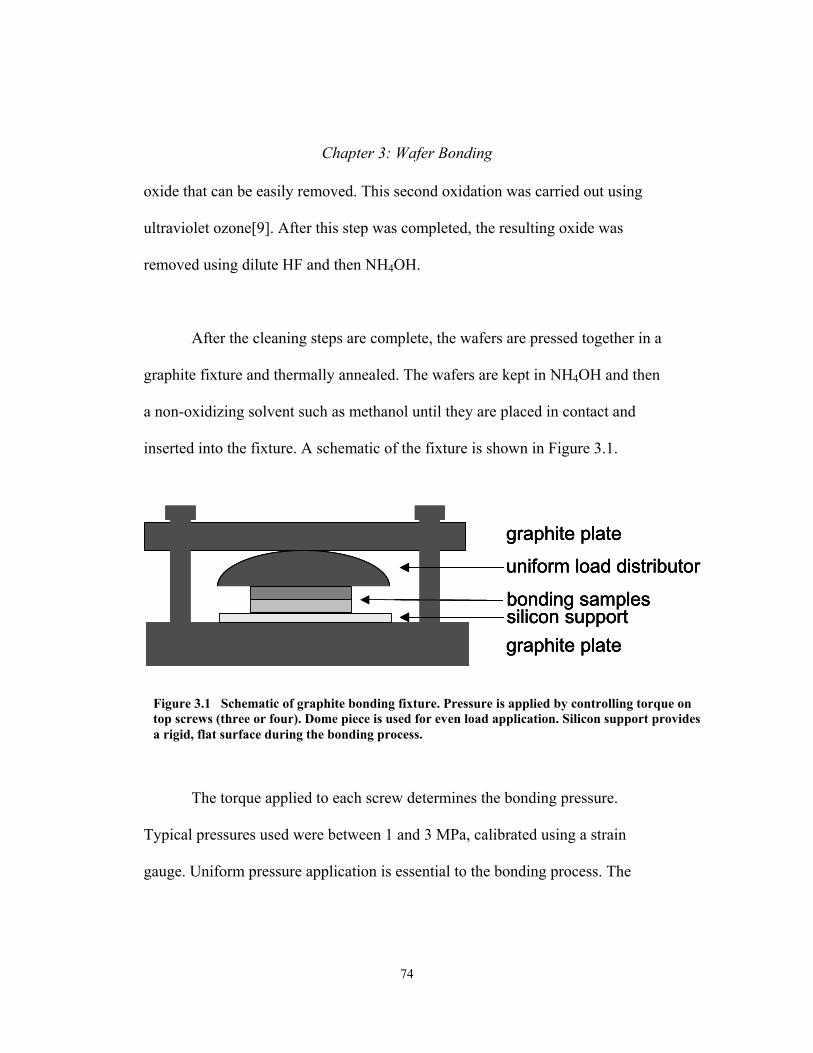
Chapter 3: Wafer Bonding
oxide that can be easily removed. This second oxidation was carried out using
ultraviolet ozone[9]. After this step was completed, the resulting oxide was
removed using dilute HF and then NH4OH.
After the cleaning steps are complete, the wafers are pressed together in a
graphite fixture and thermally annealed. The wafers are kept in NH4OH and then
a non-oxidizing solvent such as methanol until they are placed in contact and
inserted into the fixture. A schematic of the fixture is shown in Figure 3.1.
uniform load distributor
bonding samplessilicon support
graphite plate
graphite plate
uniform load distributor
bonding samplessilicon support
graphite plate
graphite plate
uniform load distributor
bonding samplessilicon support
graphite plate
graphite plate
Figure 3.1 Schematic of graphite bonding fixture. Pressure is applied by controlling torque on top screws (three or four). Dome piece is used for even load application. Silicon support provides a rigid, flat surface during the bonding process.
The torque applied to each screw determines the bonding pressure.
Typical pressures used were between 1 and 3 MPa, calibrated using a strain
gauge. Uniform pressure application is essential to the bonding process. The
74
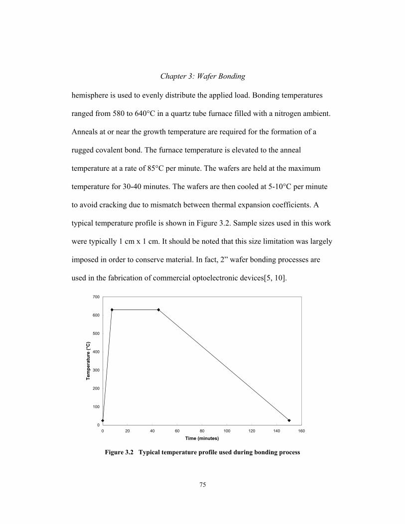
Chapter 3: Wafer Bonding
hemisphere is used to evenly distribute the applied load. Bonding temperatures
ranged from 580 to 640°C in a quartz tube furnace filled with a nitrogen ambient.
Anneals at or near the growth temperature are required for the formation of a
rugged covalent bond. The furnace temperature is elevated to the anneal
temperature at a rate of 85°C per minute. The wafers are held at the maximum
temperature for 30-40 minutes. The wafers are then cooled at 5-10°C per minute
to avoid cracking due to mismatch between thermal expansion coefficients. A
typical temperature profile is shown in Figure 3.2. Sample sizes used in this work
were typically 1 cm x 1 cm. It should be noted that this size limitation was largely
imposed in order to conserve material. In fact, 2” wafer bonding processes are
used in the fabrication of commercial optoelectronic devices[5, 10].
0
100
200
300
400
500
600
700
0 20 40 60 80 100 120 140 160
Time (minutes)
Tem
pera
ture
(°C
)
Figure 3.2 Typical temperature profile used during bonding process
75

Chapter 3: Wafer Bonding
Following the thermal anneal, one of the substrates must be removed in
order to facilitate further processing. An etch stop layer is included in the epitaxial
structures so that substrate removal terminates at the desired point. InP substrates
are removed using a 3:1 HCl:DI (deionized water) solution. This solution has an
etch rate of ~8 µm per minute and will stop on InGaAs/InGaAsP layers. These
etch stops are removed using 3:1:50 H3PO4:H2O2:DI which stops on InP. GaAs
substrates are removed using a spray etcher[11] and a 30:1 H2O2:NH4OH solution
that stops on high Al content AlGaAs layers (x>0.7). This etch stop is removed
using 1:10 HF:DI, leaving a GaAs surface exposed. In the case of a double wafer
bonded VCSEL structure, the bonding process is repeated after InP substrate and
InGaAsP etch stop removal. After the second bond, a GaAs substrate is removed.
The double bonding process is illustrated in Figure 3.3, leaving an InP epitaxial
film between two GaAs epitaxial films on a GaAs substrate.
76

Chapter 3: Wafer Bonding
p-GaAs/AlGaAs DBR p-i-n InGaAsP/InP active region undoped GaAs/AlAs DBR
Bond p-GaAs and p-InP surfaces Remove InP substrate and etch stop
Bond undoped GaAs and n-InP surfaces Remove p-GaAs substrate and etch stop
Start with three wafers:
p-GaAs/AlGaAs DBR p-i-n InGaAsP/InP active region undoped GaAs/AlAs DBR
Bond p-GaAs and p-InP surfaces Remove InP substrate and etch stop
Bond undoped GaAs and n-InP surfaces Remove p-GaAs substrate and etch stop
Start with three wafers:
p
a
i
Figure 3.3 Double bonding process, leaving InGaAsP/InP active region between two GaAs/AlGaAs DBRs on a GaAs substrate
The wafer bonding process for compound semiconductors was initially
roposed by Liau[12]. The process summarized above was developed at UCSB
nd applied to the fabrication of bonded VCSELs by numerous researchers,
ncluding Dudley, Babic, Margalit and Black. Further details on the bonding
77

Chapter 3: Wafer Bonding
process and analysis of the bonded junction can be found in their publications and
dissertations [13-16].
3.3. Structural Analysis
Scanning electron microscopy (SEM) was used to obtain information
about void density and interface quality. An image of a double-bonded VCSEL
structure is shown below. The bonded junctions appear smooth and no
deformation of the mirror periods is observed.
bonded junctionsInP active region
p-GaAs/AlGaAs DBR
n-GaAs/AlAs DBR
10 µm bonded junctionsInP active region
p-GaAs/AlGaAs DBR
n-GaAs/AlAs DBR
10 µm
Figure 3.4 Scanning electron microscopy (SEM) image of double bonded structure
78

Chapter 3: Wafer Bonding
However, more rigorous techniques are required in order to thoroughly
evaluate the bonding process. Recent collaboration between UCSB and Jin-
Phillipp at MPI-Stuttgart has resulted in a more complete understanding of bond
formation[19]. Analysis tools used by Jin-Phillipp included high-resolution
transmission electron microscopy (HRTEM) and energy dispersive x-ray
spectroscopy (EDS). During the bonding process, an edge dislocation network is
formed to relieve strain, accommodating lattice mismatch at the bonding
temperature and tilt misorientation. A third dislocation network forms during
cooling to relax thermal misfit due to the difference in thermal expansion
coefficients between GaAs and InP. Bonding at lower temperatures would reduce
the density of these dislocations. No evidence of threading dislocations was
found, confirming the observations of other authors[17, 18, 20]. TEM images of
the bonded interface are shown in Figures 3.5a and 3.5b.
79

Chapter 3: Wafer Bonding
Figure 3.5a TEM image of GaAs:InP bonded junction, courtesy of N-Y. Jin-Phillipp. Interface is of high quality with no intermediate layer.
Figure 3.5b TEM image of GaAs:InP bonded junction, courtesy of N-Y. Jin-Phillipp. Interface contains thin amorphous layer.
80
Chapter 3: Wafer Bonding
In some cases, the interface contains a thin amorphous layer as shown in
Figure 3.4. Analysis of the diffraction pattern indicates that the crystalline phase
may be α-Ga2O3. Amorphous native oxides of Ga are known to form crystalline
islands during high temperature anneals[21]. The amorphous layer is likely due to
incomplete removal of native oxide prior to the bonding process. Due to
equipment limitations, the final bond is performed in atmospheric conditions. This
inevitably results in the formation of a thin native oxide prior to bonding.
Secondary ion mass spectroscopy analysis performed by Charles Evans and
Associates confirms high oxygen content and also suggests high levels of carbon
and hydrogen, perhaps as a result of solvent cleaning or immersion in solvent
prior to bonding[8]. Although this interface layer is quite thin, it is thought to
affect the electrical characteristics of the bonded junction, as will be discussed
later in this chapter. Mobile dopants such as Zn and Be also accumulate at the
bonded interface. Significant interdiffusion of Ga, As, In, and P is observed in
EDS measurements. In diffuses deeper into GaAs layers than P and As diffuses
more deeply into InP than Ga. During the thermal anneal, group V elements P and
As dissociate from InP and GaAs, then diffuse toward the interface. Diffusion of
In is enhanced by the presence of Zn dopant. It is thought that Zn dopant atoms
may occupy In atomic sites and promote In diffusion toward and across the
81

Chapter 3: Wafer Bonding
interface. Mass transport during the high temperature process smoothes the
junction and joins separated half-planes.
3.4. Optical Analysis
The optical impact of wafer bonding is important in two respects. The
optical loss introduced by the bonded junction must be low in order to maintain an
optically transparent interface in the VCSEL structure. Additionally, the bonding
process should not degrade the optical properties of DBR and quantum well
structures. Measurements by Liu indicate that the optical loss due to the bonded
junction is no greater than 0.5 cm–1[22]. Considering the short interaction length,
the expected round trip loss contribution from the junction in a VCSEL structure
can be neglected. Cavity designs used in the course of this work placed the
bonded junctions at nulls in the standing wave pattern, further reducing possible
optical losses. The surface roughness of bonded films is comparable to that of
conventionally grown epitaxial layers, resulting in negligible scattering
losses[20]. The optical properties of wafer bonded GaAs/AlGaAs DBRs are
maintained through the bonding process, with no meaningful impact from thermal
or strain induced disordering[23]. Depth-resolved photoluminescence
measurements by Black[16] show that luminescence from both GaAs and InP
quantum well structures are reasonably well-preserved through the bonding
82

Chapter 3: Wafer Bonding
process, although there is some loss in luminescence for quantum wells and
strained quantum wells within 300 nm of the bonded junction. This material
degradation may be reduced by the use of group V (P, As) overpressure during
the bonding process. A shift in peak photoluminescence wavelength is observed.
Thermal cycling using the bonding conditions results in a blueshift. However, the
bonding process introduces a competing redshift. These effects results from a
complex combination of atomic interdiffusion, strain relaxation and defect
diffusion. The use of a superlattice barrier between quantum well regions and the
bonded junction to reduce the number of non-radiative recombination centers will
be discussed in Section 3.6 along with further details on the effects of bonding
quantum well structures.
3.5. Electrical Analysis
Carrier transport across bonded heterojunctions is also an area of interest.
Long wavelength VCSELs require low electrical resistance in order to reduce
device self-heating. This self-heating reduces carrier confinement and shifts the
optical gain peak with respect to the longitudinal cavity mode. The electrical
properties of bonded InP:GaAs junctions have been studied using current-voltage
characteristics (I-V), capacitance-voltage characteristics (C-V), admittance
spectroscopy and electron beam induced current (EBIC) measurements. Ohmic
83

Chapter 3: Wafer Bonding
conduction has been achieved for n-GaAs:n-InP bonded junctions. Admittance
spectroscopy[23] and the fitting of experimental curves to thermionic emission
models[18] indicate a conduction band offset (∆Ec) of 0.3-0.4 eV at the n-n
bonded junction. These figures are in reasonable agreement with theoretical
predictions[24, 25]. A value of 0.05 eV has been calculated for the valence band
offset (∆Ev), although the corresponding value for ∆Ec is not in agreement with
those given above[26]. A turn-on voltage of 1-2 V is observed for p-GaAs:p-InP
bonded junctions at the current densities required to support a practical device (1-
10 kA/cm2), with high resistance for hole transport. A typical I-V characteristic
for a p-GaAs:p-InP bonded junction is shown below.
0
1
2
3
0 1 2 3 4 5 6 7 8 9
Current (mA)
Volta
ge (V
)
p-GaAs substrate : p-InP epitaxy1.5 V turn-on
0
1
2
3
0 1 2 3 4 5 6 7 8 9
Current (mA)
Volta
ge (V
)
p-GaAs substrate : p-InP epitaxy1.5 V turn-on
Figure 3.6 Typical I-V characteristic for a p-p bonded junction with no active region
1010
84

Chapter 3: Wafer Bonding
This turn-on behavior is consistent with the formation of an interface
donor charge layer with density greater than 1012/cm2. These charges may be due
to an interface layer, dangling bonds or a combination of the two. The calculated
donor charge density is on the same order as the expected dangling bond density.
The precise nature of carrier interaction with this charge layer is unknown. I-V
curves suggest that low mobility holes encounter a resistive barrier. The turn-on
voltage was present in all p-GaAs:p-InP junctions fabricated, regardless of surface
preparation, doping, or contamination levels. This suggests that the contamination
levels in all fabricated devices exceed those required for improved conduction or
that the voltage drop is independent of the contamination level. A schematic band
diagram at 2 V forward bias is shown in Figure 3.7.
-6.0
-5.5
-5.0
-4.5
-4.0
-3.5
-3.0
-2.5
-2.0
0.00 0.01 0.02 0.03 0.04 0.05 0.06 0.07 0.08 0.09 0.10
Grid position (µm)
Ener
gy (e
V)
Ec
Ev
p-GaAs, 1 x 1020 cm-3 p-InP, 2 x 1018 cm-3
bonded junction
holeselectrons
hole barrier 2 V forward bias-6.0
-5.5
-5.0
-4.5
-4.0
-3.5
-3.0
-2.5
-2.0
0.00 0.01 0.02 0.03 0.04 0.05 0.06 0.07 0.08 0.09 0.10
Grid position (µm)
Ener
gy (e
V)
Ec
Ev
p-GaAs, 1 x 1020 cm-3 p-InP, 2 x 1018 cm-3
bonded junction
holeselectrons
holeselectrons
hole barrier 2 V forward bias
Figure 3.7 Representation of band diagram at p-GaAs:p-InP bonded junction
85

Chapter 3: Wafer Bonding
The interface charge layer creates a barrier to hole transport. In p-p
bonded junctions, this barrier contributes to high turn-on voltage and resistance.
In bonded VCSEL structures, the p-p junction may serve as a significant non-
radiative recombination site, due to electron overshoot of the active region. High
p-type doping or implantation may compensate the interface charge or disorder
any interface layer. In theory, perfect in-phase bonding should reduce the
interface charge density and forward voltage[27, 28]. Attempts were made to
bond p-GaAs and p-InP in orientations with matched dangling bond densities.
However, the rough surface morphology of these off-axis growths resulted in poor
bonding and a high turn-on voltage. In practice, the voltage-current characteristics
of [001] GaAs on [001] InP are orientation independent and no special care is
taken to align wafers in a particular orientation prior to bonding.
EBIC analysis has been used to measure the location and density of
electrically active defects in bonded diode structures[23]. Locally generated
electrons and holes are swept out by the built-in electric field and collected at the
device contacts. Although dark-line defects were observed at the bonded junction,
a negligible dark-line density was observed at a distance of 0.4 µm from the
interface. This suggests that the bonding process does not degrade InP structures
at a distance of 0.4 µm from the bonded interface. The VCSEL structures
86

Chapter 3: Wafer Bonding
fabricated during the course of this dissertation had gain regions positioned at an
appropriate distance from the bonded junction to reduce the likelihood of
degradation during bonding. In addition, a superlattice barrier was introduced to
reduce the number of non-radiative recombination centers in bonded InP active
regions.
3.6. Superlattice Barrier
The dislocations generated during the bonding process are not mobile at
ordinary device operating temperatures. However, these dislocations may initially
be established in unfavorable locations. Defects in the InP cladding may result in
non-radiative recombination, limiting laser efficiency. Defects residing in the
quantum well region reduce available gain and could prevent device operation
altogether. Although previous analysis showed limited defect propagation, further
methods of controlling defect generation and propagation during the bonding
process are desirable. To this end, a superlattice barrier was added to the p-InP
cladding, shown in Figure 3.8.
87
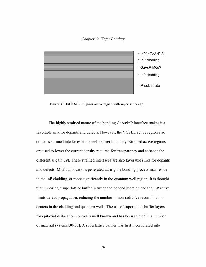
Chapter 3: Wafer Bonding
InP substrate
n-InP cladding
p-InP cladding
InGaAsP MQW
p-InP/InGaAsP SL
InP substrate
n-InP cladding
p-InP cladding
InGaAsP MQW
p-InP/InGaAsP SL
Figure 3.8 InGaAsP/InP p-i-n active region with superlattice cap
The highly strained nature of the bonding GaAs:InP interface makes it a
favorable sink for dopants and defects. However, the VCSEL active region also
contains strained interfaces at the well-barrier boundary. Strained active regions
are used to lower the current density required for transparency and enhance the
differential gain[29]. These strained interfaces are also favorable sinks for dopants
and defects. Misfit dislocations generated during the bonding process may reside
in the InP cladding, or more significantly in the quantum well region. It is thought
that imposing a superlattice buffer between the bonded junction and the InP active
limits defect propagation, reducing the number of non-radiative recombination
centers in the cladding and quantum wells. The use of superlattice buffer layers
for epitaxial dislocation control is well known and has been studied in a number
of material systems[30-32]. A superlattice barrier was first incorporated into
88

Chapter 3: Wafer Bonding
bonded InP active regions in 1999 at UCSB[33]. Results from this and subsequent
work with superlattice barrier active regions are summarized below.
During the high temperature bonding process, significant dopant and
defect diffusion takes place. Zinc is an exceptionally mobile species and diffuses
along with point defects from the active region. Strain relaxation and thermal
effects contribute to atomic interdiffusion at the well-barrier interfaces. The
bonding process introduces additional strain relaxation effects and potential
dislocations in the active region. The combination of these thermal and stress
effects can be harmful to the quality of the bonded active region.
Photoluminescence spectra from a highly strained active region without a
superlattice cap are shown in Figure 3.9. The solid line shows luminescence from
the as-grown active region. The dotted line shows luminescence from the same
active region after being thermally cycled under the temperature profile used for
bonding. No pressure was applied. A loose GaAs substrate was placed over the
sample to provide group V overpressure and prevent surface degradation. The
dashed line shows luminescence from the structure after wafer bonding to GaAs.
The InP substrate and InGaAsP etch stop have been removed. The same active
region structure was used for all three measurements.
89

Chapter 3: Wafer Bonding
0
0.05
0.10
0.15
0.20
0.25
0.30
0.35
Phot
olum
ines
cenc
e in
tens
ity (a
u)
Wavelength (nm)
Thermally cycled
As grown
Fused to GaAs wafer
1450 1500 1550 16000
0.05
0.10
0.15
0.20
0.25
0.30
0.35
Phot
olum
ines
cenc
e in
tens
ity (a
u)
Wavelength (nm)
Thermally cycled
As grown
Fused to GaAs wafer
1450 1500 1550 1600
Figure 3.9 Photoluminescence intensity from as-grown, thermally cycled and bonded active regions. The active region contained 6 strained InGaAsP quantum well between a Zn-doped p-InP cladding and a Si-doped n-InP cladding.
Thermal cycling diminishes and wavelength shifts quantum well
luminescence by encouraging atomic interdiffusion at the well-barrier interface.
Zinc diffusion through quantum wells also compromises active region integrity.
Photoluminescence from the bonded active region is severely degraded relative to
both the as-grown and thermally cycled cases. It should be noted that this was a
highly strained active region and that the degradation encountered was not typical.
It may be inferred that the decreased luminescence in the bonded active region is
not entirely due to thermal processes, since the thermally cycled active region
shows a smaller reduction in luminescence intensity. The remaining decrease is
attributed to strain relaxation processes and the possible introduction of
dislocations into the active region. The use of an intracavity superlattice was
90

Chapter 3: Wafer Bonding
initially motivated by the multiple wavelength design discussed in Section 3.7.
However, it was discovered that bonded active regions with a superlattice barrier
had enhanced luminescence compared to as-grown active regions. Results for
active regions with and without superlattice caps bonded to undoped GaAs
substrate are shown in Figure 3.10. The cap consisted of four periods of p-InP/p-
InGaAsP (λg = 1.3 µm). Each layer was 7.5 nm thick. The peak luminescence
wavelength for the superlattice was at 1270 nm. Residual luminescence near 1270
nm after superlattice removal is due to the InGaAsP etch stop layer. For samples
without a cap, the superlattice was removed using selective wet etches. Quantum
well luminescence peak is not affected by etching off the superlattice periods.
0.0E+00
5.0E-05
1.0E-04
1.5E-04
2.0E-04
2.5E-04
1200 1250 1300 1350 1400 1450 1500 1550 1600
Wavelength (nm)
Phot
olum
ines
ence
inte
nsity
(au)
Active region with superlattice
Active region with superlattice removed
Bonded active region with superlattice
Bonded active region without superlattice
superlattice
active
0.0E+00
5.0E-05
1.0E-04
1.5E-04
2.0E-04
2.5E-04
1200 1250 1300 1350 1400 1450 1500 1550 1600
Wavelength (nm)
Phot
olum
ines
ence
inte
nsity
(au)
Active region with superlattice
Active region with superlattice removed
Bonded active region with superlattice
Bonded active region without superlattice
0.0E+00
5.0E-05
1.0E-04
1.5E-04
2.0E-04
2.5E-04
1200 1250 1300 1350 1400 1450 15000.0E+00
5.0E-05
1.0E-04
1.5E-04
2.0E-04
2.5E-04
1200 1250 1300 1350 1400 1450 1500 1550 1600
Wavelength (nm)
Phot
olum
ines
ence
inte
nsity
(au)
Active region with superlattice
Active region with superlattice removed
Bonded active region with superlattice
Bonded active region without superlattice
superlattice
active
Figure 3.10 Photoluminescence from active region with superlattice and with superlattice removed. Solid lines show PL intensity prior to bonding. Dashed lines show PL intensity after bonding and substrate removal.
91

Chapter 3: Wafer Bonding
Active region luminescence is not only preserved by the addition of an
intracavity superlattice; it is enhanced! It is believed that the superlattice acts as a
defect-blocking layer. Although misfit dislocations are still generated by the
bonding process, the superlattice blocks their propagation into the InP cladding
and active region. The concept of strain relaxation and defect accumulation in the
superlattice layers is supported by the decreased luminescence from the bonded
superlattice. Under thermal cycling, the strained well-barrier interfaces are the
most favorable sink for dopants and active region defects. During bonding, the
highly strained GaAs:InP interface is also a highly attractive gettering center.
Without a superlattice barrier, the bonding junction acts as a net source for
defects, gettering active region defects but generating misfit dislocations. With a
superlattice barrier, the propagation of misfit dislocations is blocked and the
bonding junction behaves as a net defect sink, increasing active region
photoluminescence. The enhanced luminescence suggests that bonded VCSELs
fabricated with superlattice-capped active regions will have fewer non-radiative
recombination centers, resulting in higher internal and differential efficiencies.
These expectations were confirmed in multiple generations of devices[34].
VCSEL design and results will be discussed extensively in Chapters 4 and 5.
92

Chapter 3: Wafer Bonding
Although experiments were conducted with superlattices at both bonding
interfaces, the superlattice is thought to be more relevant during the first bonding
than the second. Intuitively, the first bond is less forgiving than the second since
roughly equal amounts of material with dissimilar lattice constants are being
bonded. However, the second bond is performed under more elastic conditions,
with only a thin layer of mismatched material between GaAs substrates and
unstrained epitaxial layers. These conditions are thought to be less conducive to
dislocation formation, particularly after the strain relaxation processes that take
place during the first bond.
It is possible for the superlattice structure to be further optimized. Due to
material limitations, only the four period superlattice described above was used in
bonding experiments and VCSEL fabrication. Varying the superlattice
composition or number of periods could yield improved results. Strained-layer
superlattices (SLS) have been used extensively as buffer layers in mismatched
heteroepitaxy[35] and may be effective during the bonding process as well. These
SLS structures create a strain field, causing impinging dislocations to be bent
along the superlattice interface planes. Further investigation should include
varying superlattice conditions and probing of the bonded superlattice and
surfaces to confirm defect accommodation.
93
Chapter 3: Wafer Bonding
3.7. Multiple Wavelength Cavity Definition
The intracavity superlattice discussed above may also be used to define
multiple cavity wavelengths prior to bonding. Different numbers of superlattice
periods are removed in adjacent regions using selective wet etches. This creates a
physical cavity length difference between neighboring cavities that results in
different lasing wavelengths for neighboring devices. This tuning method was
proposed by Jayaraman and used to fabricate optically pumped, multiple
wavelength VCSEL arrays by depositing dielectric mirrors over the patterned
surface and bottom DBR[36]. Although these were 1.55 µm VCSEL arrays,
external optical pumping is undesirable for low cost sources as it adds cost and
complexity. The primary contribution of this dissertation is the fabrication of
electrically pumped, directly modulated multiple wavelength VCSEL arrays using
an intracavity superlattice tuning layer prior to wafer bonding. The array elements
share the same active region and DBRs.
Due to the short cavity length, only a small perturbation is required to shift
the cavity mode. The amount of the shift is determined by the effective cavity
length of the VCSEL and the optical path length of the material removed. In this
work, a 3λ/2 active region was used. This thickness was chosen in order to
94

Chapter 3: Wafer Bonding
distance the quantum well region from the bonded junction while still providing a
low loss cavity. Using the one-dimensional transfer matrix method[39], the
expected shift in cavity wavelength for removal of InP and InGaAsP (λg = 1.3
µm) material from this active region was calculated. The nominal cavity
wavelength was 1550 nm. Results are plotted below. The change in slope between
the two curves is due to the difference in refractive index between the two
materials. The curvature of the shift characteristic is due to the greater
perturbation caused by removal of a given amount of material in a shorter cavity.
-35
-30
-25
-20
-15
-10
-5
0
0 5 10 15 20 25 30 35 40 45 50
Thickness removed (nm)
Wav
elen
gth
shift
(nm
)
InPInGaAsP (1.3 µm)
3λ/2 active region
Nominal cavity wavelength = 1550 nm
-35
-30
-25
-20
-15
-10
-5
0
0 5 10 15 20 25 30 35 40 45 50
Thickness removed (nm)
Wav
elen
gth
shift
(nm
)
InPInGaAsP (1.3 µm)
3λ/2 active region
Nominal cavity wavelength = 1550 nm
Figure 3.11 Wavelength shift versus thickness of InP or InGaAsP material removed
95
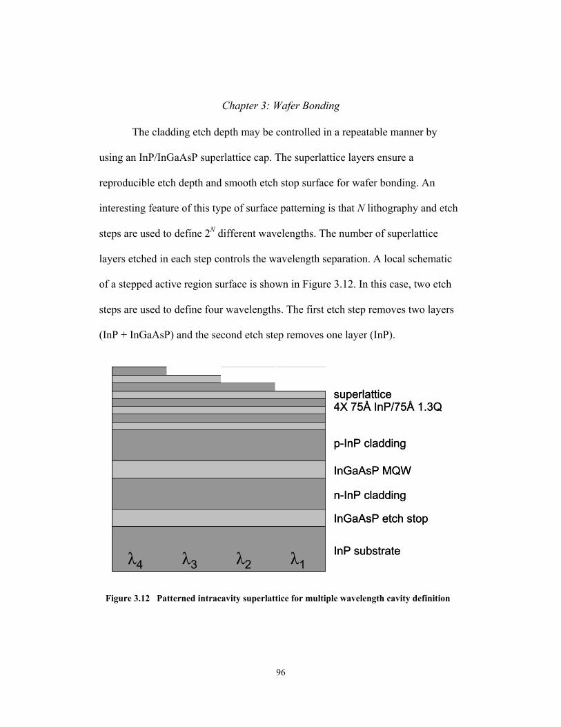
Chapter 3: Wafer Bonding
The cladding etch depth may be controlled in a repeatable manner by
using an InP/InGaAsP superlattice cap. The superlattice layers ensure a
reproducible etch depth and smooth etch stop surface for wafer bonding. An
interesting feature of this type of surface patterning is that N lithography and etch
steps are used to define 2N different wavelengths. The number of superlattice
layers etched in each step controls the wavelength separation. A local schematic
of a stepped active region surface is shown in Figure 3.12. In this case, two etch
steps are used to define four wavelengths. The first etch step removes two layers
(InP + InGaAsP) and the second etch step removes one layer (InP).
InP substrate
InGaAsP etch stop
n-InP cladding
InGaAsP MQW
p-InP cladding
superlattice
λ4 λ3 λ2 λ1
4X 75Å InP/75Å 1.3Q
InP substrate
InGaAsP etch stop
n-InP cladding
InGaAsP MQW
p-InP cladding
superlattice
λ4 λ3 λ2 λ1
4X 75Å InP/75Å 1.3Q
Figure 3.12 Patterned intracavity superlattice for multiple wavelength cavity definition
96

Chapter 3: Wafer Bonding
The superlattice layers may be removed using selective wet etches. The
etch chemistry of the InGaAsP/InP system has been well characterized[37]. InP
may be etched in H3PO4:HCl. The etch rate as a function of the H3PO4:HCl ratio
is shown in Figure 3.13
0
50
100
150
200
250
300
350
400
450
1 2 3 4 5 6 7 8
H3PO4:HCl ratio
InP
Etch
Rat
e (Å
/sec
ond)
0
50
100
150
200
250
300
350
400
450
1 2 3 4 5 6 7 8
H3PO4:HCl ratio
InP
Etch
Rat
e (Å
/sec
ond)
99
Figure 3.13 Etch rate of InP in H3PO4:HCl solutions
No etch rate was observed for InGaAsP in these solutions for times up to
20 minutes. Low H3PO4:HCl ratio solutions may etch too quickly and punch
through the thin InGaAsP layers. High H3PO4:HCl ratio solutions are quite
viscous and may not rinse cleanly. For device fabrication, the 75 Å InP layers
97
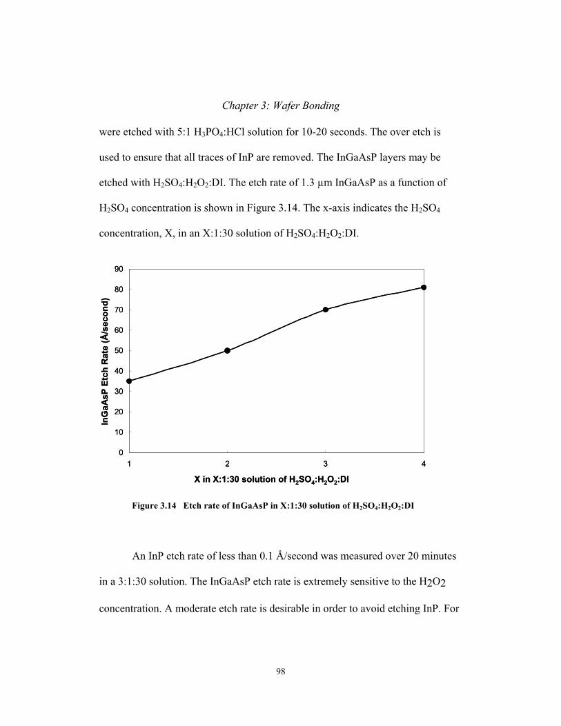
Chapter 3: Wafer Bonding
were etched with 5:1 H3PO4:HCl solution for 10-20 seconds. The over etch is
used to ensure that all traces of InP are removed. The InGaAsP layers may be
etched with H2SO4:H2O2:DI. The etch rate of 1.3 µm InGaAsP as a function of
H2SO4 concentration is shown in Figure 3.14. The x-axis indicates the H2SO4
concentration, X, in an X:1:30 solution of H2SO4:H2O2:DI.
0
10
20
30
40
50
60
70
80
90
1 2 3 4
X in X:1:30 solution of H2SO4:H2O2:DI
InG
aAsP
Etc
h R
ate
(Å/s
econ
d)
0
10
20
30
40
50
60
70
80
90
1 2 3 4
X in X:1:30 solution of H2SO4:H2O2:DI
InG
aAsP
Etc
h R
ate
(Å/s
econ
d)
Figure 3.14 Etch rate of InGaAsP in X:1:30 solution of H2SO4:H2O2:DI
An InP etch rate of less than 0.1 Å/second was measured over 20 minutes
in a 3:1:30 solution. The InGaAsP etch rate is extremely sensitive to the H2O2
concentration. A moderate etch rate is desirable in order to avoid etching InP. For
98
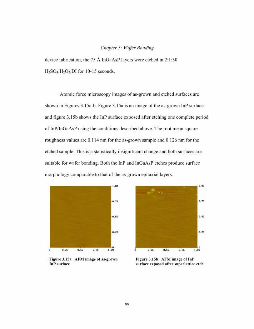
Chapter 3: Wafer Bonding
device fabrication, the 75 Å InGaAsP layers were etched in 2:1:30
H2SO4:H2O2:DI for 10-15 seconds.
Atomic force microscopy images of as-grown and etched surfaces are
shown in Figures 3.15a-b. Figure 3.15a is an image of the as-grown InP surface
and figure 3.15b shows the InP surface exposed after etching one complete period
of InP/InGaAsP using the conditions described above. The root mean square
roughness values are 0.114 nm for the as-grown sample and 0.126 nm for the
etched sample. This is a statistically insignificant change and both surfaces are
suitable for wafer bonding. Both the InP and InGaAsP etches produce surface
morphology comparable to that of the as-grown epitaxial layers.
Figure 3.15a AFM image of as-grownInP surface
99
Figure 3.15b AFM image of InP surface exposed after superlattice etch

Chapter 3: Wafer Bonding
An AFM image of an etched trough is shown in Figure 3.16. The etch
depth is 15 nm, corresponding to one superlattice period. The individual layers
were etched after separate lithographic steps. This accounts for the ripple near the
trough sidewall. Both the top and bottom surfaces appear smooth and featureless,
providing confirmation of the etch depth and quality.
Figure 3.16 AFM image of 15 nm deep trough etched in superlattice layers
100

Chapter 3: Wafer Bonding
After surface patterning, the active region is bonded as described in
Section 3.2. The etched channel grid is used as an alignment layer for the step
height etch. The first bond is to the patterned p-cladding surface. After InP
substrate removal, the rest of the bonding process proceeds normally. Although
the surface appears to be highly non-planar in the exaggerated schematic of
Figure 3.12, the actual bowing of the bonded DBR is quite small. The lateral pitch
is chosen as 250 µm to facilitate fiber coupling using standard components.
Choosing a step height of 150 Å between devices and assuming that any bowing
is evenly distributed over the 250 µm distance yields a bowing angle of 6.0 x 10⁻⁵
radians. In the worst-case scenario, it is assumed that the entire step height is
accounted for over an etched channel of width 10 µm. This assumption yields a
bowing angle of 1.50 x 10⁻³ radians. These angles are quite small and are not
expected to alter the expected DBR reflectivity or cavity wavelength.
The expected shift in wavelength for cavities containing different numbers
of superlattice periods may be calculated using the one-dimensional transfer
matrix method[38]. The difference in refractive index between InP and 1.3 µm
InGaAsP at 1550 nm is sufficiently small that the additional reflections
introduced are insignificant. The wavelength shift versus number of layers
removed is shown in Figure 3.17. The cavity is 3λ/2 in length, with cladding
101
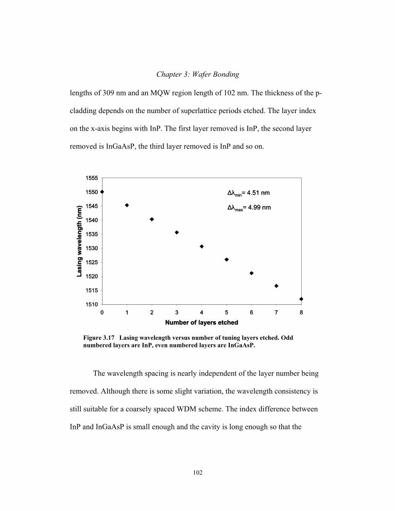
Chapter 3: Wafer Bonding
lengths of 309 nm and an MQW region length of 102 nm. The thickness of the p-
cladding depends on the number of superlattice periods etched. The layer index
on the x-axis begins with InP. The first layer removed is InP, the second layer
removed is InGaAsP, the third layer removed is InP and so on.
∆λmin= 4.51 nm
∆λmax= 4.99 nm
1510
1515
1520
1525
1530
1535
1540
1545
1550
1555
0 1 2 3 4 5 6 7
Number of layers etched
Lasi
ng w
avel
engt
h (n
m)
∆λmin= 4.51 nm
∆λmax= 4.99 nm
1510
1515
1520
1525
1530
1535
1540
1545
1550
1555
0 1 2 3 4 5 6 7
Number of layers etched
Lasi
ng w
avel
engt
h (n
m)
88
rem
stil
InP
Figure 3.17 Lasing wavelength versus number of tuning layers etched. Odd numbered layers are InP, even numbered layers are InGaAsP.
The wavelength spacing is nearly independent of the layer number being
oved. Although there is some slight variation, the wavelength consistency is
l suitable for a coarsely spaced WDM scheme. The index difference between
and InGaAsP is small enough and the cavity is long enough so that the
102

Chapter 3: Wafer Bonding
changes made to round trip optical path length by each layer are roughly equal.
For this cavity length and tuning structure, an additional 5 Å in each InP layer
would be required to exactly equalize the wavelength shift caused by etching an
individual layer. This is an unreasonable growth tolerance. A finer degree of
control may be achieved more practically by using thicker cladding layers. This
would permit the use of thicker tuning layers to achieve the same wavelength shift
that required thinner layers previously. Growth tolerances on these thicker layers
would be sufficient to allow equalization of wavelength spacing for odd and even
layer number removals.
In order to support multiple wavelength operation, VCSEL DBRs must
have sufficient bandwidth to provide peak reflectivity for all channels. The large
bandwidth of GaAs/AlGaAs DBRs at 1.55 µm was discussed in Section 2.3.2. In
Figure 3.18, four cavity modes at 1520, 1530, 1540 and 1550 nm are
superimposed on the measured reflectivity spectrum of a 25.5 period
GaAs/Al0.9Ga0.1As DBR.
103

Chapter 3: Wafer Bonding
0
0.1
0.2
0.3
0.4
0.5
0.6
0.7
0.8
0.9
1
1400 1450 1500 1550 1600 1650 1700
Wavelength (nm)
Ref
lect
ivity
0
0.1
0.2
0.3
0.4
0.5
0.6
0.7
0.8
0.9
1
1400 1450 1500 1550 1600 1650 1700
Wavelength (nm)
Ref
lect
ivity
allows
phase c
usable
nm/°C.
reflecti
reliably
wavele
Figure 3.18 Reflectivity spectrum of 25.5 period GaAs/Al0.9Ga0.1As DBR.Mode positions at 1520, 1530, 1540 and 1550 nm are indicated by arrows.
All four wavelengths are comfortably within the DBR stop band. This
each wavelength to utilize the DBR at near-peak reflectivity with minimal
ontribution. Although the DBR bandwidth is approximately 150 nm, the
portion of the bandwidth is limited by thermal wavelength drift of 0.1
As lasing wavelengths move toward the edge of the stop band, mirror
vity becomes more sensitive to environmental fluctuations. In order to
and uniformly operate all wavelengths, it is desirable to limit the
ngth span to 60 nm or less. Active cooling would allow for operation over
104
Chapter 3: Wafer Bonding
a wider wavelength range. Although all four channels appear to have high
reflectivities in the figure above, it should be emphasized that this is only a
qualitative examination of DBR reflectivity versus wavelength. A more rigorous
evaluation of mode detuning, reflectivity reduction and the corresponding change
in threshold current will be presented in Chapter 4.
The material gain of InGaAsP quantum well active regions over the
desired wavelength span must also be considered. Similar active regions grown at
UCSB have supported tuning spans of more than 70 nm in sampled grating DBR
lasers without separate amplification[39]. External cavity InGaAsP multiquantum
well lasers have been used to demonstrate 200 nm tuning[40]. Although these
geometries are not identical to the VCSEL structure considered in this work, they
are representative of the wide gain bandwidth available in the InGaAsP system.
Quantum well lasers are particularly well-suited for operation over a wide
wavelength span. Multiple quantized states can provide nearly constant gain over
an extended spectral range provided that the current density is sufficiently
high[41]. Since elements of the array will lase with different mode-gain offsets,
some non-uniformity is expected. However, the broad gain peak of InGaAsP
MQW regions is expected to minimize these effects. Figure 3.19 shows the
photoluminescence spectra from an active region with six strained quantum wells
105
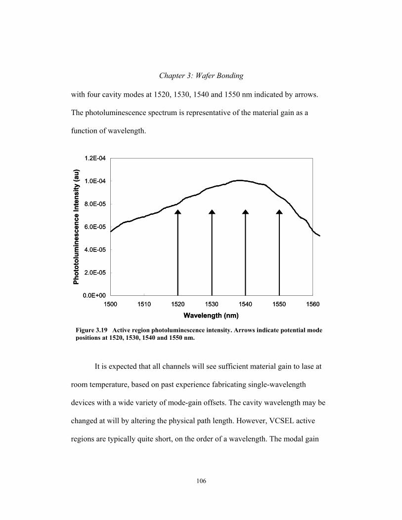
Chapter 3: Wafer Bonding
with four cavity modes at 1520, 1530, 1540 and 1550 nm indicated by arrows.
The photoluminescence spectrum is representative of the material gain as a
function of wavelength.
0.0E+00
2.0E-05
4.0E-05
6.0E-05
8.0E-05
1.0E-04
1.2E-04
1500 1510 1520 1530 1540 1550 1560
Wavelength (nm)
Phot
otol
umin
esce
nce
Inte
nsity
(au)
0.0E+00
2.0E-05
4.0E-05
6.0E-05
8.0E-05
1.0E-04
1.2E-04
1500 1510 1520 1530 1540 1550 1560
Wavelength (nm)
Phot
otol
umin
esce
nce
Inte
nsity
(au)
d
c
r
Figure 3.19 Active region photoluminescence intensity. Arrows indicate potential modepositions at 1520, 1530, 1540 and 1550 nm.
It is expected that all channels will see sufficient material gain to lase at
room temperature, based on past experience fabricating single-wavelength
evices with a wide variety of mode-gain offsets. The cavity wavelength may be
hanged at will by altering the physical path length. However, VCSEL active
egions are typically quite short, on the order of a wavelength. The modal gain
106

Chapter 3: Wafer Bonding
will be significantly reduced if there is no longer sufficient spatial overlap
between the optical field and the quantum well region. A thorough analysis of
gain, loss, standing wave effects and mode detuning will be presented in Chapter
4.
The WDM VCSEL array described in this chapter has similar loss levels
for each channel, limited by standing wave non-uniformity. Tunable diode lasers
typically require the introduction of additional cavity loss to shift the lasing
wavelength. This necessitates the use of complicated gain and phase control
schemes. Although multiple wavelength VCSEL arrays don’t have the same
functionality as tunable lasers, reduced fabrication and control costs should make
them attractive alternatives for low cost WDM systems.
3.8. Electrical Characteristics
In consideration of the terraced bonding surface, it must be determined if
current transport is possible at all four step heights and what degree of uniformity
is attainable. A key element in successful bonding of the patterned active region is
determining the proper pressure to apply. If the applied force was too high, the
wafers were adversely impacted, including cracking or degradation of quantum
107

Chapter 3: Wafer Bonding
well luminescence. If the applied force was too low, device yield was limited by
microscopic and macroscopic voids, even more so than during a planar bonding
process. It was found that applied pressures of 2-3 MPa were appropriate for
bonding patterned active regions. These pressures are 25-50% higher than those
used to join unpatterned surfaces at UCSB. In order to evaluate the diode turn-on
voltage and series resistance, a patterned active region was bonded to a p-GaAs
epitaxial layer on a p-GaAs substrate, as shown in Figure 3.20.
InP substrate
InGaAsP etch stop
n-InP cladding
InGaAsP MQW
p-InP cladding
superlattice
λ4 λ3 λ2 λ1
4X 75Å InP/75Å 1.3Q
p-GaAs substrate
InP substrate
InGaAsP etch stop
n-InP cladding
InGaAsP MQW
p-InP cladding
superlattice
λ4 λ3 λ2 λ1
4X 75Å InP/75Å 1.3Q
p-GaAs substrate
Figure 3.20 Bonding of p-i-n diode structure to determine electrical characteristics of multiple wavelength structures
108
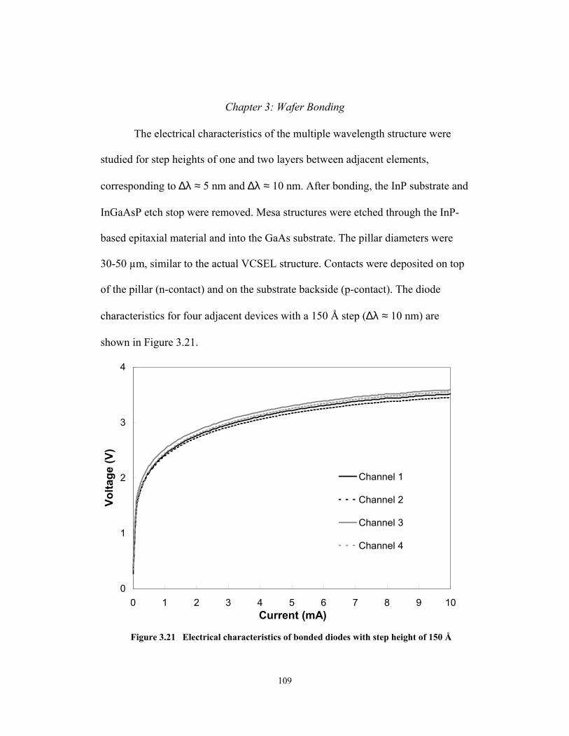
Chapter 3: Wafer Bonding
The electrical characteristics of the multiple wavelength structure were
studied for step heights of one and two layers between adjacent elements,
corresponding to ∆λ ≈ 5 nm and ∆λ ≈ 10 nm. After bonding, the InP substrate and
InGaAsP etch stop were removed. Mesa structures were etched through the InP-
based epitaxial material and into the GaAs substrate. The pillar diameters were
30-50 µm, similar to the actual VCSEL structure. Contacts were deposited on top
of the pillar (n-contact) and on the substrate backside (p-contact). The diode
characteristics for four adjacent devices with a 150 Å step (∆λ ≈ 10 nm) are
shown in Figure 3.21.
0
1
2
3
4
0 1 2 3 4 5 6 7 8 9 1Current (mA)
Volta
ge (V
)
Channel 1
Channel 2
Channel 3
Channel 4
Figure 3.21 Electrical characteristics of bonded diodes with step height of 150 Å
0
109

Chapter 3: Wafer Bonding
The electrical characteristics are consistent with those expected from
single wavelength p-i-n diodes with a p-GaAs:p-InP bonded junction. Channel 1
is the shortest device and channel 4 is the longest device. There is no systematic
difference between diode turn-on voltage or resistance and channel number for
any of the multiple arrays tested. The bonding quality, as indicated by the turn-on
voltage, is similar across the array. The series resistance is also near constant. At
3 V, the current density is 4 kA/cm2, more than sufficient for lasing. Although
each device sees a different number of electrically resistive superlattice periods,
this is only a small part of the total resistance in the structure. Significantly, these
results indicate that uniform electrical transport is possible across a patterned
junction with a step height of 150 Å. Similar results were obtained for diodes with
a 75 Å step height.
3.9. Summary
In this chapter, the process of wafer bonding was described. Structural,
optical and electrical properties of the bonded junction were summarized. The use
of a novel superlattice defect-blocking layer was found to preserve and even
enhance the luminescence of InGaAsP quantum wells in bonded InP active
regions. A patterned InP/InGaAsP superlattice was proposed as an intracavity
110

Chapter 3: Wafer Bonding
tuning layer in a double bonded VCSEL. The electrical characteristics of these
patterned and bonded active regions are suitable for continuous-wave lasing.
Further analysis of single and multiple wavelength VCSEL cavities will be
presented in Chapter 4.
References
[1] J. W. Matthews and A. E. Blakeslee, "Defects in epitaxial multilayers. I.
Misfit dislocations," Journal of Crystal Growth, vol. 27, pp. 118-25, 1974.
[2] J. Boucart, C. Starck, F. Gaborit, A. Plais, N. Bouche, E. Derouin, J. C.
Remy, J. Bonnet-Gamard, L. Goldstein, C. Fortin, D. Carpentier, P. Salet,
F. Brillouet, and J. Jacquet, "Metamorphic DBR and tunnel-junction
injection. A CW RT monolithic long-wavelength VCSEL," IEEE Journal
of Selected Topics in Quantum Electronics, vol.5, pp. 520-9, 1999.
[3] C. Starck, A. Plais, E. Derouin, A. Pinquier, F. Gaborit, C. Fortin, L.
Goldstein, J. Boucart, P. Salet, D. Carpentier, and J. Jacquet, "Fabrication
of 1.55 µm oxidized VCSELs with top metamorphic GaAs/AlGaAs and
bottom InP/InGaAsP Bragg reflectors," Conference Proceedings, 1998
International Conference on Indium Phosphide and Related Materials, pp.
369-72, 1998.
111

Chapter 3: Wafer Bonding
[4] A. R. Hawkins, W. Weishu, P. Abraham, K. Streubel, and J. E. Bowers,
"High gain-bandwidth-product silicon heterointerface photodetector,"
Applied Physics Letters, vol. 70, pp. 303-5, 1997.
[5] I. H. Tan, D. A. Vanderwater, J. W. Huang, G. E. Hofler, F. A. Kish, E. I.
Chen, and T. D. Ostentowski, "Wafer bonding of 75 mm diameter GaP to
AlGaInP-GaP light-emitting diode wafers," Journal of Electronic
Materials, vol. 29, pp. 188-94, 2000.
[6] A. Karim, P. Abraham, D. Lofgreen, Y. J. Chiu, J. Piprek, and J. E.
Bowers, "Wafer bonded 1.55 µm vertical cavity lasers with continuous
wave operation up to 105°C," Applied Physics Letters, vol. 78, pp. 2632-3,
2001.
[7] D. I. Babic, J. E. Bowers, E. L. Hu, L. Yang, and K. Carey, "Wafer fusion
for surface-normal optoelectronic device applications," International
Journal of High Speed Electronics and Systems, vol. 8, pp. 357-76, 1997.
[8] K. A. Black, "Fused Long-Wavelength Vertical-Cavity Lasers," in
Materials Department. Santa Barbara, CA: University of California, 2000.
[9] Z. H. Lu, B. Bryskiewicz, J. McCaffrey, Z. Wasilewski, and M. J.
Graham, "Ultraviolet-ozone oxidation of GaAs(100) and InP(100),"
Journal of Vacuum Science & Technology B (Microelectronics Processing
and Phenomena), vol. 11, pp. 2033-7, 1993.
112

Chapter 3: Wafer Bonding
[10] V. Jayaraman, J. C. Geske, M. H. MacDougal, T. D. Lowes, F. H. Peters,
D. VanDeusen, T. C. Goodnough, S. P. Kilcoyne, and D. Welch, "High
temperature 1300 nm VCSELs for single-mode fiber-optic
communication," 1999 Digest of the LEOS Summer Topical Meetings, vol.
3, pp. 19-20, 1999.
[11] H. Tanobe, F. Koyama, and K. Iga, "Etching and optical characteristics in
GaAs/GaAlAs surface emitting laser fabrication using a novel spray etch,"
Japanese Journal of Applied Physics, Part 1 (Regular Papers & Short
Notes), vol. 31, pp. 1597-601, 1992.
[12] Z. L. Liau and D. E. Mull, "Wafer fusion: a novel technique for
optoelectronic device fabrication and monolithic integration," Applied
Physics Letters, vol. 56, pp. 737-9, 1990.
[13] J. J. Dudley, "Wafer Fused Vertical Cavity Lasers," in Electrical and
Computer Engineering. Santa Barbara, CA: University of California,
Santa Barbara, 1994.
[14] D. I. Babic, "Double-fused long-wavelength vertical-cavity lasers," in
Electrical and Computer Engineering. Santa Barbara, CA: University of
California, Santa Barbara, 1995.
[15] N. M. Margalit, J. Piprek, S. Zhang, D. I. Babic, K. Streubel, R. P. Mirin,
J. R. Wesselmann, and J. E. Bowers, "64°C continuous-wave operation of
113

Chapter 3: Wafer Bonding
1.5-µm vertical-cavity laser," IEEE Journal of Selected Topics in
Quantum Electronics, vol. 3, pp. 359-65, 1997.
[16] A. Black, A. R. Hawkins, N. M. Margalit, D. I. Babic, A. L. Holmes, Jr.,
Y. L. Chang, P. Abraham, J. E. Bowers, and E. L. Hu, "Wafer fusion:
materials issues and device results," IEEE Journal of Selected Topics in
Quantum Electronics, vol. 3, pp. 943-51, 1997.
[17] G. Patriarche, F. Jeannes, J. L. Oudar, and F. Glas, "Structure of the
GaAs/InP interface obtained by direct wafer bonding optimised for surface
emitting optical devices," Journal of Applied Physics, vol. 82, pp. 4892-
903, 1997.
[18] H. Wada, Y. Ogawa, and T. Kamijoh, "Electrical characteristics of
directly-bonded GaAs and InP," Applied Physics Letters, vol. 62, pp. 738-
40, 1993.
[19] N. Y. Jin-Phillipp, W. Sigle, A. Black, D. Babic, J. Bowers, E. L. Hu, and
M. Ruhle, "Interface of directly bonded GaAs and InP," Journal of
Applied Physics, vol. 89, pp. 1017-1024, 2001.
[20] R. J. Ram, J. J. Dudley, J. E. Bowers, L. Yang, K. Carey, S. J. Rosner, and
K. Nauka, "GaAs to InP wafer fusion," Journal of Applied Physics, vol.
78, pp. 4227-37, 1995.
114

Chapter 3: Wafer Bonding
[21] H. L. Hartnahel, "Properties of Gallium Arsenide," 2nd ed. London, UK:
INSPEC, p. 369, 1990.
[22] B. Liu, A. Shakouri, P. Abraham, K. Boo-Gyoun, A. W. Jackson, and J. E.
Bowers, "Fused vertical couplers," Applied Physics Letters, vol. 72, pp.
2637-8, 1998.
[23] R. J. Ram, L. Yang, K. Nauka, Y. M. Houng, M. Ludowise, D. E. Mars, J.
J. Dudley, and S. Y. Wang, "Analysis of wafer fusing for 1.3 µm vertical
cavity surface emitting lasers," Applied Physics Letters, vol. 62, pp. 2474-
6, 1993.
[24] J. M. Langer and H. Heinrich, "Deep-level impurities: a possible guide to
prediction of band-edge discontinuities in semiconductor heterojunctions,"
Physical Review Letters, vol. 55, pp. 1414-17, 1985.
[25] D. D. Nolte, "Type II to type I conversion of pseudomorphic GaAs on InP
dependent on growth direction," Journal of Vacuum Science &
Technology B (Microelectronics Processing and Phenomena), vol. 7, pp.
820-3, 1989.
[26] F. Salomonsson, K. Streubel, J. Bentell, M. Hammar, D. Keiper, R.
Westphalen, J. Piprek, L. Sagalowicz, A. Rudra, and J. Behrend, "Wafer
fused p-InP/p-GaAs heterojunctions," Journal of Applied Physics, vol. 83,
pp. 768-74, 1998.
115

Chapter 3: Wafer Bonding
[27] Y. Okuno, M. Aoki, T. Tsuchiya, and K. Uomi, "Fabrication of (001) InP-
based 1.55-µm wavelength lasers on a (110) GaAs substrate by direct
bonding (a prospect for free-orientation integration)," Applied Physics
Letters, vol. 67, pp. 810-12, 1995.
[28] Y. Okuno, K. Uomi, M. Aoki, T. Taniwatari, M. Suzuki, and M. Kondow,
"Anti-phase direct bonding and its application to the fabrication of InP-
based 1.55 µm wavelength lasers on GaAs substrates," Applied Physics
Letters, vol. 66, pp. 451-3, 1995.
[29] L. A. Coldren and S. Corzine, Diode Lasers and Photonic Integrated
Circuits. New York, NY: John Wiley & Sons, Inc., 1995.
[30] G. A. Rozgonyi, P. M. Petroff, and M. B. Panish, "Elimination of
dislocations in heteroepitaxial layers by the controlled introduction of
interfacial misfit dislocations," Applied Physics Letters, vol. 24, pp. 251-4,
1974.
[31] S. Einfeldt, H. Heinke, V. Kirchner, and D. Hommel, "Strain relaxation in
AlGaN/GaN superlattices grown on GaN," Journal of Applied Physics,
vol. 89, pp. 2160-7, 2001.
[32] J. S. Kim, S. H. Suh, C. H. Kim, and S. J. Chung, "Defect reduction in
ZnMgSSe epilayers on GaAs by using ZnMgSe/ZnSSe strained-layer
superlattices," Solid State Communications, vol. 100, pp. 817-20, 1996.
116

Chapter 3: Wafer Bonding
[33] K. A. Black, P. Abraham, A. Karim, J. E. Bowers, and E. L. Hu,
"Improved luminescence from InGaAsP/InP MQW active regions using a
wafer fused superlattice barrier," Conference Proceedings of Eleventh
International Conference on Indium Phosphide and Related Materials
(IPRM ’99), pp. 357-60, 1999.
[34] A. Karim, K. A. Black, P. Abraham, D. Lofgreen, Y. J. Chiu, J. Piprek,
and J. E. Bowers, "Superlattice barrier 1528-nm vertical-cavity laser with
85°C continuous-wave operation," IEEE Photonics Technology Letters,
vol. 12, pp. 1438-40, 2000.
[35] H. Kawanami, "Heteroepitaxial technologies of III-V on Si," Solar Energy
Materials and Solar Cells, vol. 66, pp. 479-86, 2001.
[36] V. Jayaraman and M. Kilcoyne, "WDM array using long-wavelength
vertical cavity lasers," Proc. SPIE, vol. 2690, pp. 325-36, 1996.
[37] S. Adachi, "Properties of indium phosphide," London: INSPEC, 1991.
[38] F. Peters, "Vertical," version 1.0, Lompoc, CA, 1995.
[39] B. Mason, J. Barton, G. A. Fish, L. A. Coldren, and S. P. Denbaars,
"Design of sampled grating DBR lasers with integrated semiconductor
optical amplifiers," IEEE Photonics Technology Letters, vol. 12, pp. 762-
4, 2000.
117

Chapter 3: Wafer Bonding
118
[40] A. Lidgard, T. Tanbun-Ek, R. A. Logan, H. Temkin, K. W. Wecht, and N.
A. Olsson, "External-cavity InGaAs/InP graded index multiquantum well
laser with a 200 nm tuning range," Applied Physics Letters, vol. 56, pp.
816-17, 1990.
[41] M. Mittelstein, D. Mehuys, A. Yariv, J. E. Ungar, and R. Sarfaty,
"Broadband tunability of gain-flattened quantum well semiconductor
lasers with an external grating," Applied Physics Letters, vol. 54, pp.
1092-4, 1989.

Chapter 4: Device Design and Fabrication
4. Device Design and Fabrication
4.1. Introduction
In this chapter, the design and fabrication processes for wafer bonded 1.55
µm VCSELs are outlined. Mirror reflectivities and the number of quantum wells
in the gain region are chosen to satisfy requirements for low threshold current and
reasonable output power. Round trip gain and loss are considered, including
standing wave effects. The impact of mode detuning is used to determine growth
tolerances for individual lasers and the tuning range for multiple wavelength
devices. Optical and electrical confinement schemes are discussed. A half-
intracavity design is used in order to provide uniform carrier injection while
reducing optical loss. The lithographic, etch and deposition procedures used to
fabricate the device are described.
p-GaAs/Al0.9Ga0.1As DBR
p-i-n InP/InGaAsP MQW/InP
nid GaAs/AlAs DBR
semi-insulating GaAs substrate
p-contactoxide aperture
n-contact
top-emitting
Si3N4 passivation
p-GaAs/Al0.9Ga0.1As DBR
p-i-n InP/InGaAsP MQW/InP
nid GaAs/AlAs DBR
semi-insulating GaAs substrate
p-contactoxide aperture
n-contact
top-emitting
Si3N4 passivation
Figure 4.1 Wafer-bonded VCSEL structure
119

Chapter 4: Device Design and Fabrication
4.2. Gain Enhancement Factor
One of the most striking differences between edge-emitting lasers and
VCSELs is the disparity in cavity length. A typical edge-emitting laser is
hundreds of microns long. A VCSEL cavity may be on the order of a micron in
length, with the gain region occupying a fraction of that distance. Although the
gain length is short in a VCSEL, three major effects combine to make the actual
threshold material gain levels for edge-emitting lasers and VCSELs comparable.
These are:
• Increased lateral confinement of the optical mode
• High reflectivity
• Standing wave gain enhancement
The increased lateral confinement is due to the unique VCSEL geometry.
The optical mode overlaps the gain region over a large portion of the waveguide,
rather than just a small fraction as in an edge-emitting laser. The typical mirror
reflectivities for a VCSEL are greater than 99%. The non-transmissive DBR
usually has a reflectivity in excess of 99.9%, while the reflectivity of the
transmissive DBR is chosen to strike a balance between low threshold current and
high output power. The active regions used in this work were 3λ/2 in length. This
120

Chapter 4: Device Design and Fabrication
cavity length was chosen to place the active region at a suitable distance from the
bonded junction and at the central standing wave peak. Since the emitted light is
coherent on this length scale, standing wave effects must be considered. In order
to calculate the gain or loss from a thin section, the mean value of the electric
field intensity must be calculated by integrating the field over the layer and
dividing by the length of the section. The standing wave effects in the active
region are accounted for by the gain enhancement factor, ξenh[1]
dxxn
L
Lx
Lx
effenh
2cos2 2
2
20
0
∫+
−
=
λπ
ξ Equation 4.1
where L is the length of the section, x0 is the distance between the standing wave
peak and the center of the active region, neff is the effective refractive index and λ
is the free space wavelength. The analytic solution to this integral is given by
( ) (
−+
++= 00 2
2sin2
2sin
41 xL
nxL
nLn
effeff
effenh λ
πλ
ππ
λξ ) Equation 4.2
Altering the cladding thickness on one side of the active region will shift
the location of the standing wave peak in the VCSEL cavity. Equation 4.2 may be
used to calculate the change in gain enhancement factor that results from shifting
the standing wave peak from the center of the active region. The standing wave
121

Chapter 4: Device Design and Fabrication
peak could be kept in the center of the active region by patterning superlattices on
both sides of the active region. However, proper design eliminates the need for
this extra processing. The gain enhancement factor can be as high as 2 for very
short gain regions and quickly converges to a value of 1 for lengths much longer
than a wavelength. In Figure 4.2, the gain enhancement factor is plotted versus
gain region thickness for a centered standing wave (x0 = 0), λ = 1550 nm and
neff = 3.3.
0
0.5
1
1.5
2
0 100 200 300 400 500 600 700 800 900 1000
Active region thickness (nm)
Gai
n en
hanc
emen
t fac
tor
Figure 4.2 Plot of gain enhancement factor versus gain region layer thickness
The standing wave effect in a short cavity permits the gain region to be
positioned in such a way as to increase the effective gain by a factor of 2. In
122

Chapter 4: Device Design and Fabrication
practice, this value is less than 2 due to the finite thickness of the gain region. The
gain regions used in this work were 102 nm in length. This corresponds to ξenh =
1.7 for the conditions described above. Removing superlattice tuning layers will
change the value of x0 for devices with different wavelengths. It must be
determined if this affects the gain enhancement factor. If this factor is altered
appreciably between devices, there will be significant performance variation
within the array.
Position (nm)
Nor
mal
ized
Fie
ld In
tens
ity (a
u)R
efractive Index
10
12
14
16
18
20
3
3.2
3.4
3.6
3.8
4
8280 8300 8320 8340 8360 8380 8400
Position (nm)
Nor
mal
ized
Fie
ld In
tens
ity (a
u)R
efractive Index
10
12
14
16
18
20
3
3.2
3.4
3.6
3.8
4
8280 8300 8320 8340 8360 8380 8400
Figure 4.3 Central standing wave peaks for 1520, 1530, 1540 and 1550 nm cavity modes in 3λ/2 active region with 6 quantum wells. Active region index profile is plotted to indicate spatial overlap with quantum wells. Shortest wavelength peak (1520 nm) is furthest toward the left. Longest wavelength peak (1550 nm) is furthest toward the right.
123

Chapter 4: Device Design and Fabrication
In Figure 4.3, the central standing wave peaks for 1520, 1530, 1540 and
1550 nm cavity modes in a 3λ/2 active region are plotted along with the refractive
index profile. The active region has 6 quantum wells, centered for a 1535 nm
cavity mode. By choosing the cladding layer thickness properly, the standing
wave peaks for all wavelengths may be well-aligned with the gain region. This is
illustrated graphically in Figure 4.3, where the spatial overlap is similar for all
four wavelengths under consideration. In Figure 4.4, the gain enhancement factor
is plotted versus wavelength using the same parameters as above. This factor now
depends on active region thickness and x0, which is different for each wavelength.
1.60
1.65
1.70
1.75
1.80
1520 1525 1530 1535 1540 1545 1550
Gai
n En
hanc
emen
t Fac
tor
Wavelength (nm)Figure 4.4 Gain enhancement factor versus wavelength in 3λ/2 active region designed for maximum overlap at 1535 nm
124

Chapter 4: Device Design and Fabrication
For a well-designed cavity, the gain enhancement factor varies by less
than 3%. The uncertainty in material gain and internal quantum efficiency are
both greater than 3%. This indicates that standing wave effects are not significant
contributors to device non-uniformity. Variation in the gain enhancement factor
could be reduced further by using a longer cavity or by tuning both cladding
layers as mentioned previously.
4.3. Threshold Current
An appropriate set of design curves would show the current needed to
reach threshold and the desired peak output power over a range of VCSEL
parameters. A simple set of expressions may be used to generate these curves and
determine the right number of quantum wells and the proper reflectivity for the
output DBR. Although this model is only one-dimensional and neglects device
self-heating, it still provides useful design information. The expressions used are
adapted from well-known relationships between gain, loss, reflectivity, current
density and output power[1]. The threshold material gain, gth, is given by the
expression
+=+Γ
RLdNdNg effibbwwth
1ln)( αξ Equation 4.3
125

Chapter 4: Device Design and Fabrication
where Γ is the optical confinement factor, ξ is the gain enhancement factor, Nw is
the number of quantum wells, dw is the well thickness, Nb is the number of
arriers, db is the barrier thickness, αi is the internal cavity loss (assumed to be
s.
,
is the active region length. The cladding length, L , is
that the lasing wavelength is 1550 nm. λ0
ace wavelength, ∆nt is the index difference in the top mirror, ∆nb is
the ind
b
equally distributed), Leff is the effective cavity length considering field penetration
depth into the mirrors, and R is the mean power reflectivity of the two DBR
This expression for modal gain includes gain enhancement, modal confinement
internal loss and mirror loss. Leff and R are given by
btcbbwweff nn ∆∆ 44
bt RRR =
LdNdNL ++++= )( 00 λλEquation 4.4
Equation 4.5
The first term in Leff
chosen for each active region length so
c
is the free sp
ex difference in the bottom mirror, Rt is the reflectivity of the top mirror
and Rb is the reflectivity of the bottom mirror. This approximation for DBR
penetration depth is valid in the case of strongly reflective gratings. The material
gain is related to radiative current density by the following expression:
126

Chapter 4: Device Design and Fabrication
where g is the material gain as a function of current density, g0 is a gain
parameter, J is the current density and Jtr is the transparency current density for
0 and Jtr may be obtained through calculat
omparison with actual data. This expression may be used to obtain the threshold
current is
iciency,
where ηi is the internal quantum efficiency. The radiative current required to reach
P, can be expressed as
each well. Values for g ion or
c
current density once the threshold material gain is known. The threshold
simply given by the product of the threshold current density and the active area.
Assuming that all light is exiting through one mirror, the differential eff
ηD is given by
+
L
R
effi1ln
ln
α
a particular output power,
PqII λ0+=
=
R
iD
1
ηη
Dthp hc η
)ln()( 0 JNgJg =
trw
JEquation 4.6
Equation 4.7
Equation 4.8
127
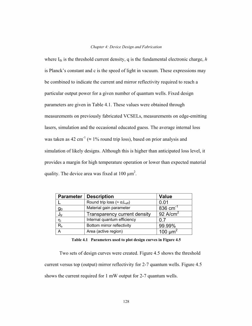
Chapter 4: Device Design and Fabrication
where Ith is the threshold current density, q is the fundamental electronic charge, h
is Planck’s constant and c is the speed of light in vacuum. These expressions may
be combined to indicate the current and mirror reflectivity required to reach a
particular output power for a given number of quantum wells. Fix
parameters are given in Table 4.1. These values were obtained through
lasers, simulation and the occasional educated guess. The average internal loss
was taken as 42 cm (≈ 1% round trip loss), based on prior analysis and
simulation of likely designs. Although this is higher than anticipated loss level, it
provides a margin for high temperature operation or lower than expected material
quality. The device area was fixed at 100 µm .
Parameter Description Value
ed design
measurements on previously fabricated VCSELs, measurements on edge-emitting
-1
2
L Round trip loss (≈ α iLeff) 0.01 -1
Jtr Transparency current density 92 A/cm2
Rb Bottom mirror reflectivity
g0 Material gain parameter 836 cm
η i Internal quantum efficiency 0.7 99.99%
A Area (active region) 100 µm2 Table 4.1 Parameters used to plot design curves in Figure 4.5
e
curren sus top (o an Figure 4.5
shows current req 2-7 quant ells.
Two sets of design curves were cr ated. Figure 4.5 shows the threshold
t ver utput) mirror reflectivity for 2-7 qu tum wells.
the uired for 1 mW output for um w
128

Chapter 4: Device Design and Fabrication
1
2
4
0.985 0.987 0.989 0.991 0.993 0.995 0.997 0.999
Top mirror reflectivity
3
Thre
shol
d cu
rren
t (m
A)
wells = 7
5wells = 2wells = 3wells = 4wells = 5wells = 6
129
5
6
7
8
9
10
0.985 0.987 0.989 0.991 0.993 0.995 0.997 0.999
Top mirror reflectivity
Cur
rent
for 1
mW
out
put (
mA
)
wells = 2wells = 3wells = 4wells = 5wells = 6wells = 7
Figure 4.5 Threshold current versus top mirror reflectivity for Nw = 2-7
Figure 4.6 Current for 1 mW output versus top mirror reflectivity for Nw = 2-7

Chapter 4: Device Design and Fabrication
130
rror
reflectivity at
operating with higher reflectivities supports lasing over a wider wavelength span,
4.4.
im
which is a critical issue for multiple wavelength arrays.
Mode Detuning
The position of the cavity resonance is rarely in perfect alignment with the
peak DBR reflectivity. Although the DBR reflectivity is quite high over a wide
range, cavity modes at different points in the stop band will encounter different
reflectivities and have different threshold currents. This has important
plications for single wavelength, multiple wavelength and tunable devices.
specification was presented in Section 2.5. It will also be seen th
As mentioned earlier, this simple model neglects device self-heating,
which reduces the gain for a particular injection level. Increased gain is also
desirable to support lasing at elevated ambient temperatures. Current spreading,
which increases threshold current from the ideal one-dimensional value, has also
been neglected. These effects can be mitigated somewhat by using higher mi
reflectivities at the expense of output power. Increasing the number of quantum
wells can compensate for poor material quality or spatial misalignment of the gain
region. The devices fabricated in this work contained either 5 or 6 quantum wells
with top mirror reflectivities of 99.3-99.5%. A p-DBR design matching this

Chapter 4: Device Design and Fabrication
Variati o
or a
ed
, it is likely that the
avity wavelength is detuned from the peak reflectivity wavelengths of both
ld current is more sensitive to a reflectivity reduction
in the output mirror. It is assumed that the reflectivity variation is contained
entirely within the transmissive DBR. This reduction in overall reflectivity
corresponds to a reduction in output mirror reflectivity from 99.30% to 98.78%,
assuming a 99.95% reflective bottom DBR. Using the equations presented in
Chapter 2, it is found that this includes the wavelength span of 1507-1593 nm for
a DBR centered at 1550 nm. This 86 nm bandwidth is more than enough to
ons in epitaxial layer thickness will inevitably detune the cavity mode t
some degree for an individual device. The reflectivity bandwidth for multiple
wavelength and tunable devices must be sufficiently uniform to permit operation
over the desired wavelength span without large increases in threshold current. An
appropriate figure of merit might be the maximum wavelength span over which
the threshold current varies by less than 20%.
The first step is to establish the change in reflectivity that results in a
threshold variation of 20%. Using the equations above and the design curve f
six quantum well device with a mean power reflectivity of .9960, it is determin
that a reduction of the mean power reflectivity to .9934 would cause a 20%
increase in threshold current. In a double bonded VCSEL
c
DBRs. However, the thresho
131
Chapter 4: Device Design and Fabrication
support multiple wavelength operation over the EDFA gain bandwidth (1530-
1560 nm). The fractional bandwidth of 5.54% suggests that DBR layer thickne
may vary by ±5.54% before the threshold current changes by 20%.
The relationship of the cavity mode to the reflectivity spectrum is only
part of the story. The material gain also varies
ss
with wavelength. Although there
are no simple analytic formulas for the gain spectrum of a quantum well active
region, of
where J is the current density and Jtr is the total transparency current density.
Consider an active region pumped with two different current densities, 1.2
kA/cm2 and 1.44 kA/cm2, 20% higher. Using Equation 4.9 and previous
numerical modeling of quantum well gain spectra[2, 3], the following curve fits
are derived for the two injection levels:
a polynomial curve fit may be used to approximate gain as a function
wavelength over the interval of interest. The peak material gain as a function of
current density is written using the standard logarithmic form:
trJJ
322 )1550(00834.)1550(792.0)1550(861.8)(),(:kA/cm 44.1 −−−−−−= λλλλ JgJg
)ln()( 0gJg =
322 )1550(00673.)1550(595.0)1550(993.2)(),(: kA/cm 2.1 −−−−−+= λλλλ JgJg
Equation 4.9
132

Chapter 4: Device Design and Fabrication
where g is in cm-1 and λ is in nm. The added polynomial is centered around 15
nm, which is taken as the peak gain wavelength. Although not exact, these curves
are representative of the gain variation with wavelength at the two in
50
jection
levels. Using g0 = 836 cm-1 and Jtr = 92 A/cm2 as in the previous section, the gain
bandwi
-1)
dth that defines a 20% variation in threshold current may be extracted
from the curves in Figure 4.7.
2300
2400
2500 Threshold + 20%= 1.44 kA/cm2
gth
2300
2400
2500 Threshold + 20%= 1.44 kA/cm2
gth
Wavelength (nm)
1600
1700
1800
1510 1520 1530 1540 1550 1560 1570
Threshold = 1.2 kA/cm2
Wavelength (nm)
1600
1700
1800
1510 1520 1530 1540 1550 1560 1570
Threshold = 1.2 kA/cm2
Gai
n (c
m
2000
2100
Gai
n (c
m
2000
2100
1900
2200
2600
1580
∆λ = 34 nm
-1)
1900
2200
2600
1580
∆λ = 34 nm
Figure 4.7 Gain curves for two different current densities, showing the bandwidth over which threshold current density varies by 20%
133

Chapter 4: Device Design and Fabrication
The two curves show gain as a function of wavelength for current densities of 1.2
kA/cm2 (assumed to be threshold) and 1.44 kA/cm2 (threshold + 20%). It is
assumed that the cavity mode is aligned with the gain peak at 1550 nm, as
indicated by the vertical arrow. The threshold gain value of 2300 cm-1 at 1.2
kA/cm2 for a 1550 nm cavity mode may be achieved over the range of 1532-15
nm at 1.44 kA/cm2. This sugge
66
sts that the wavelength may be varied over a 34 nm
in the InGaAsP/InP
material system have been studied extensively[5, 6]. The adoption of strained
quantum wells has reduced transparency current densities while increasing
Quantum well active regions for 1.55 µm lasers
span with only a 20% increase in threshold due to the gain profile. Fortuitously,
this span coincides nearly perfectly with EDFA gain bandwidth. The VCSEL
tuning range is limited by the gain variation with wavelength rather than by DBR
reflectivity. A more flat gain profile could be created by using a chirped quantum
well active region with each well providing peak gain at a different wavelength.
This technique is also of interest for reduced temperature sensitivity[4]. However,
a wider gain distribution will result in higher threshold currents. An optimized
solution considering the desired cavity mode(s), reflectivity spectrum and gain
spectrum may be determined for single or multiple wavelength operation based on
the desired output characteristics.
134
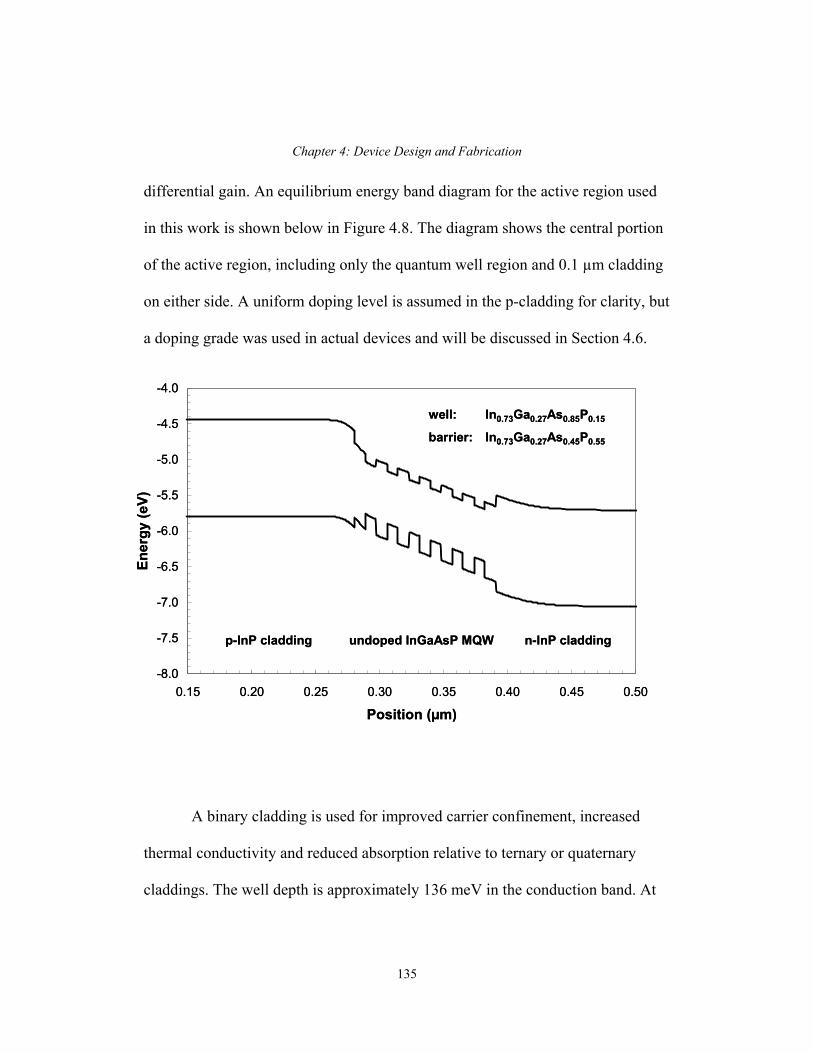
Chapter 4: Device Design and Fabrication
differential gain. An equilibrium energy band diagram for the active region used
in this work is shown below in Figure 4.8. The diagram shows the central po
of the active region, including only the quantum well region and 0.1 µm cla
on either side. A uniform doping level is assumed in the p-cladding f
rtion
dding
, but
d
. At
or clarity
a doping grade was used in actual devices and will be discussed in Section 4.6.
Figure 4.8 Band diagram of VCSEL active region at equilibrium
-8.0
-7.5
-7.0
-6.5
-6.0
-5.5
Position (µm)
well: In0.73Ga0.27As0.85P0.15
barrier: In0.73Ga0.27As0.45P0.55
p-InP cladding n-InP claddingundoped InGaAsP MQW
-5.0
-4.5
-4.0
0.15 0.20 0.25 0.30 0.35 0.40 0.45 0.50
Ener
gy (e
V)
-8.0
-7.5
-7.0
-6.5
-6.0
-5.5
Position (µm)
well: In0.73Ga0.27As0.85P0.15
barrier: In0.73Ga0.27As0.45P0.55
p-InP cladding n-InP claddingundoped InGaAsP MQW
-5.0
-4.5
-4.0
0.15 0.20 0.25 0.30 0.35 0.40 0.45 0.50
Ener
gy (e
V)
A binary cladding is used for improved carrier confinement, increase
thermal conductivity and reduced absorption relative to ternary or quaternary
claddings. The well depth is approximately 136 meV in the conduction band
135

Chapter 4: Device Design and Fabrication
InGaAsP heterojunctions, only 40% of the band offset is accommodated in the
conduction band[7]. Electron leakage could be reduced significantly by using an
AlInGaAs active region. In this material system, 68% of the band offset takes
place in the conduction band. This would dramatically improve carrier
confinement, particularly at high temperature. Carrier leakage and thermal effects
by guiding bation. A
all degree of current confinement is introduced by injection through a finite
contact nd
in fabricated devices will be examined more closely in Chapter 5.
4.5. Confinement
The discussion to this point has been focused on issues of gain, loss and
reflectivity. The precise VCSEL geometry and current injection scheme selected
also have a large impact on device performance. An advantage of using GaAs-
based DBRs in long wavelength VCSELs is that the robust lateral confinement
techniques of short wavelength VCSELs may be applied. The three types of
lateral confinement to be considered are mode confinement, current confinement
and carrier confinement. Confinement of the optical mode reduces optical losses
photons along the desired axis through a lateral index pertur
sm
area. However, increased confinement is desirable for efficient lasing a
improved spatial overlap between the mode and the gain. Carrier confinement
may be achieved with a lateral bandgap step in the active region. This increase in
136
Chapter 4: Device Design and Fabrication
bandgap limits carrier diffusion out of the active region. Carrier confinement in
VCSELs is generally difficult to achieve without complicated processing that
might eliminate the cost advantages associated with the vertical cavity geometr
Advanced techniques for mode and current confinement have been deve
GaAs-based short wavelength VCSELs. The etched pillar and oxide aperture have
enabled tremendous performance advances in threshold current and
y.
loped for
wallplug
fficiency[8, 9]. These techniques have been adapted for wafer bonded VCSELs
S d Margalit[11]. The etched pillar alone confines the
current
to
e
at UC B by Babic[10] an
to an area defined by the pillar. However, this design is entirely gain-
guided. The optical mode encounters significant loss at the pillar sidewalls
without any index guiding for photon confinement. Etching through the active
region results in significant non-radiative recombination due to the existence of
surface states. The fabrication of small, low-threshold devices is difficult due
this non-radiative recombination mechanism and the high optical loss associated
with the optical mode filling the width of the pillar. These effects are reduced
dramatically by the introduction of an oxide aperture. After etching through the
top DBR and active region, a high aluminum content AlGaAs layer is laterally
oxidized at temperatures of 400-500°C using steam. Pure AlAs is difficult to
oxidize reproducibly. The oxidation rate is more easily controlled for layers
containing small amounts of gallium, e.g. Al0.98Ga0.02As. Only one oxide aperture
137

Chapter 4: Device Design and Fabrication
is desired. The other AlGaAs layers in the DBR have x=90% so that the oxidatio
rate is negligible compared to that of the x=98% layer. The insulating aluminu
oxide layer forces current inward to the unoxidized AlGaAs region. The lateral
index perturbation from the oxide confines the optical mode in the center of the
pillar, reducing optical loss at pillar sidewalls and enabling spatial overlap
between the mode and gain profile. The aperture is usually placed at or near a
in order to reduce diffraction loss[12]. Thin, tapered apertures may be used to
reduce scattering loss[9]. A schematic of an oxidized DBR aperture is shown i
Figure 4.9.
n
m
null
n
GaAs
0.9 0.1
GaAs
Al0.9Ga0.1As
Al0.98Ga0.02As,
injected current
Al Ga As
GaAs
laterally oxidized
GaAs
optical mode
GaAs
0.9 0.1
GaAs
Al0.9Ga0.1As
Al0.98Ga0.02As,
injected current
Al Ga As
GaAs
laterally oxidized
GaAs
optical mode
Figure 4.9 Lateral current and mode confinement with oxidized AlGaAs aperture. The
confinement in the center of the pillar. bold black line illustrates the confined optical mode. The arrows show current
138

Chapter 4: Device Design and Fabrication
It should be noted that current aperturing is far more effective for
confining hole current than for electron current. The high mobility of electrons
limits n-side aperturing, as the electron current will spread again quickly after
passing through the aperture. However, hole current may be well-confined over a
greater distance due to lower hole mobility. The effects of current spreading
beneath the aperture have been studied by other authors[13] and will be examined
more closely in Chapter 5.
4.6. Opti
cal Loss
In the previous section, gain and bandwidth were calculated based on a
cm
n
GaAs doped at 2x10 cm is 58 cm –1.
ormalized to a 1018 cm-3 doping level. For instance, the absorptive loss in p-
18 -3
round trip loss level of 1%, corresponding to an effective loss coefficient of 42
-1 for a 3λ/2 cavity. The origin of these losses is now presented in further
detail. Although light emitted at 1.55 µm is below the bandgap energy for both
GaAs and InP, free carrier absorption and intervalence band absorption (IVBA) in
doped GaAs and InP are significant loss contributors. The absorptive losses at
three different wavelengths are summarized in Table 4.2. The losses are
139

Chapter 4: Device Design and Fabrication
Materi µm al 0.98 µm 1.3 µm 1.55
p-GaAs 7 cm 15 cm 29 cm
-1 -1 -1
n-InP - 5 cm-1 5 cm-1
-1 -1 -1
p-InP - 15 cm-1 15 cm-1
n-GaAs 5 cm 6 cm 6 cm
18 -3Table 4.2 Absorptive loss per 10 cm doping level for GaAs and InP at 0.98, 1.3 and 1.55 µm
Two major trends are apparent. First, the absorption losses in p-type
aterial are greater than in n-type material for the same doping level. Second, the
x with wavelength due to IVBA. Since long wavelength
VCSELs require low optical loss and low electrical resistance, these effects
combine to severely limit the range of doping levels that can be used. Fortunately,
the impact of these optical losses can be mitigated by placing highly doped layers
at nulls in the standing wave pattern. The effective absorption coefficient, αeff, is
defined by the following expression[14]:
material i f ient from Table 4.2 and ξ is the gain
enhancement factor defined in Section 4.2. The factor (2-ξ) may be thought of as
m
loss e hibits an increase
where α is the mater al loss coe fic
materialeff αξα )2( −= Equation 4.10
140

Chapter 4: Device Design and Fabrication
a loss reduction factor. H DBR sect he bonded re
tanding wave nu cavity, where the lo reduction
between 0.01 and 0.1. Although the bonded junction is not intrinsically lossy, it is
ing site for dopants, pa cularly Zn, that contribute to optical absorption.
able 4.3 summarizes the calculated optical loss in each section of the
wafer b
actor is shown as multiplying the
interaction length. The absorption loss in the MQW region is based on estimates
vary based on the injected
ighly doped ions and t junctions a
placed at s lls in the ss factor is
a getter rti
T
onded VCSEL. Interaction lengths are determined by standing wave
effects and effective DBR penetration depths. The absorptive loss in the DBRs
was calculated using the 1-D transfer matrix method. For the p-DBR, the doping
layer given corresponds to that used in the seven DBR periods closest to the
active region. The complete doping profile can be found in Section 2.7. The p-
cladding was grown using three different dopant levels to reduce zinc damage and
absorption near the quantum well region. An absorption level of 2 cm-1 is chosen
for undoped material. The loss reduction f
current. of carrier density at threshold and will
141

Chapter 4: Device Design and Fabrication
Region Material Doping (cm-3) Interaction Loss Round
(%)
p-cladding p-InP/InGaAsP 2E18 30*0.06 30 0.001% p-cladding p-InP 1E18/5E17/nid 260 15/7.5/2 0.04%
n-cladding n-InP 2E18 310 10 0.06%
length (nm) (cm-1) trip loss
p-DBR p-GaAs/Al0.9Ga0.1 As 4E17/6E17 897 12 0.21%
MQW nid-InGaAsP nid 102*1.72 50 0.18%
nid DBR nid-GaAs/AlAs nid 805 2 0.03% Total 0.52%
4.7. tructur
he desired
and confinement s
simulation, wafer b
Standing w
superlattice cap (c
contribution of the
devices with differ
round trip loss. Re
absorption, but als
junction injection
during growth, this
regions.
S
T
Table 4.3 Calculated losses in VCSEL structure
the
e
cavity length, number of quantum wells, mirror reflectivity
cheme have been determined using a combination of
onding constraints and past work with short wavelength
ave factors are used to calculate the loss contribution from
lose to null) and the MQW active region (at peak). The loss
superlattice cap is negligible and may be taken as constant for
ent wavelengths. The p-DBR is the single largest contributor to
ducing the doping levels in the DBR further would reduce
o increase the electrical resistance of the device. Tunnel
would allow the use of two n-type DBRs. Due to diffusion
transport scheme is not possible using Zn-doped active
142

Chapter 4: Device Design and Fabrication
devices. Cu tion throu s ord res
uniform carrier profile and use lateral confinement for fabrication of low
d onal s ral issues re cluding choi
he EL should be bottom-em and the n-contact l .
mission direction chosen depends on the ty e of packaging that will be used.
op-emitting devices may be epoxied to TO headers or a simple chip tray. A
bottom
r
tical
on
tion are:
• 3λ/2 cavity • 6 quantum well active region at standing wave peak
op GaAs/Al0.9Ga0.1 As DBR with 99.3% reflectivity • undoped bottom GaAs/AlAs DBR with 99.9% reflectivity
• oxide aperture for mode and current confinement at standing wave
• superlattice tuning layer near standing wave null
rrent injec gh the p-DBR i desirable in er to p ent a
threshold evices. Additi tructu main, in the ce of
whether t VCS top or itting ocation
The e p
T
-emitting device will need to be flip-chip bonded or mounted upside down
on drive circuitry, a more complicated process. Coplanar ground-signal-ground
bond bands are desirable for high-speed modulation. A p-bondpad may be
deposited on insulating material and connected to a p-contact on top of the DBR
using bridge metal. In this geometry, an intracavity n-contact permits coplana
bondpads and allows the use of an undoped bottom DBR, which reduces op
loss. Processing is complicated only slightly by the need to stop the pillar etch
the n-InP cladding. In summary, the major features of the VCSEL under
considera
• p-type t
• etched pillar to n-InP cladding
null
• p-contact on p-DBR
143

Chapter 4: Device Design and Fabrication
• n-contact on n-InP cladding
These properties may be combined in a single design. The refractive ind
profile and standing wave pattern are shown below in the vicinity of an active
region with two superlattice periods. This cavity wavelength is in the middle of
the tuning range.
3.8
3.6
3.2
80
40
oxide aperture
superlattice tuning
3.8
3.6
3.2
80
40
3.8
3.6
3.2
3.8
3.6
3.2
80
40
oxide aperture
superlattice tuning
• coplanar ground-signal-ground bond pads for high speed modulation
ex
F gure 4.10 Standing wave pattern nei ar VCSEL active region
4.0
3.4
3.0
2.8
120
100
60
20
0
Ref
ract
ive
Inde
xField Intensity (au)
0 0 920076 0 7800 8200 8400 8600 8800 900800076 0 7800 8200 8400 8600 8800 900800076 0 7800 8200 8400 8600 8800 9008000
bonded junctionbonded junction
4.0
3.4
3.0
2.8
120
100
60
20
0
Ref
ract
ive
Inde
xField Intensity (au)
0 0 9200
4.0
3.4
3.0
2.8
4.0
3.4
3.0
2.8
120
100
60
20
0
Ref
ract
ive
Inde
xField Intensity (au)
0 0 9200
bonded junctionbonded junction
Position (nm)Position (nm)Position (nm)
144
Chapter 4: Device Design and Fabrication
T q e central standing wave peak in the
λ/2 active region. Bonded junctions are located at the second null. The
superla
s.
ear a standing wave null reduces the associated optical loss.
etched into the surface of the p-cladding. These channels allow the escape of
trapped gas and liquid during the bonding process. The channel pitch is 250 µm
and the etch depth is 150-200 nm. Although the exact thickness is not critical, the
he uantum wells are located at th
3
ttice tuning layers are located on the InP side of the p-InP:p-GaAs bonded
junction and are only slightly displaced from the null. Since the superlattice
heterojunctions can be highly resistive, it is desirable to heavily dope these layer
Placing them at or n
The tapered oxide aperture is located near the third null. This allows an index
perturbation while reducing scattering and diffraction loss. The p-DBR
heterojunctions are graded as described in Chapter 2.
4.8. Fabrication
In this section, the fabrication process is outlined with a general
description of each step.
4.8.1. Wafer Bonding
The bonding process is completed as described in Chapter 3. The sample
size is typically 1 cm x 1 cm. Prior to bonding, a grid-like pattern of channels is
145

Chapter 4: Device Design and Fabrication
channels should not impinge upon the quantum well region. It is important to
make sure that the channels run all the way to the edge of the sample.
gure 4.11 Etched channels on surface of p-cladding. ChanneFi l pitch is 250 µm. Channeldepth is 150 nm.s, the surface etches described in Chapter 3 are performed
prior to he
in Figure 4.12 and an SEM image in Figure 4.13.
For WDM array
bonding to create multiple wavelength cavities. A schematic of t
bonded structure is shown
p-GaAs/Al0.9Ga0.1As DBR
p-i-n InP/InGaAsP MQW/InP
nid GaAs/AlAs DBR
semi-insulating GaAs substrate
p-GaAs/Al0.9Ga0.1As DBR
p-i-n InP/InGaAsP MQW/InP
nid GaAs/AlAs DBR
146
semi-insulating GaAs substrate
Figure 4.12 Schematic of double-bonded VCSEL structure on GaAs substrate

Chapter 4: Device Design and Fabrication
bonded junctions
p-GaAs/AlGaAs DBRp-GaAs/AlGaAs DBR
InP active region
undoped GaAs/AlAs DBR
InP active region
undoped GaAs/AlAs DBR
4.12 SEM image of double-bonded VCSEL s
10 µm bonded junctions10 µm
Figure tructure
After the GaAs substrate is etched away, it is critical that the AlGaAs etch
stop lay
. Any
he
next step. Remaining surface debris should be carefully removed. Although
er be promptly and completely removed. This layer will oxidize quickly
upon exposure. After etch stop removal, the p-GaAs contact layer is exposed
residual oxide or AlGaAs will degrade the quality of the p-contact formed in t
bonding is rarely achieved at the very edges of the sample, the bonded area
typically covers more than 90% of the surface. The surface morphology of the
bonded sample is critical. Poor morphology will lead to complications and poor
yield in all remaining process steps. Nomarski micrographs at 50x magnification
of three surface morphologies are shown in Figures 4.13a-c. The images are of the
147

Chapter 4: Device Design and Fabrication
exposed p-DBR surface after double bonding and substrate removal. Figure 4.13a
cracking seen in Figure 4.13c are caused by unevenly applied pressure or
particulate contamination during bonding. The surfaces in these images were
patterned for multiple wavelength definition prior to the first bond.
shows a good surface with only a small number of point defects. The channel
pattern is visible, indicating a slight bowing of the transferred epitaxial material.
The surface in Figure 4.13b has a high density of microscopic voids, on the order
of 1 µm in diameter. These voids are thought to be caused by trapped gas at the
bonded interface and can be prevented by using deeper channels or otherwise
forcing out all trapped liquid prior to bonding. The large-scale bubbling and
b c
Figure 4.13a-c Nomarski micrographs of exposed surfaces after double bonding process. From left to right: good surface, high microscopic void density, large-scale cracking
After bonding,
multiple wavelength de
a
identical processing steps ar
vices.
148
e used to fabricate single or

Chapter 4: Device Design and Fabrication
4.8.2. p-metallization
The p-contact resistance is much greater than the n-contact resistance a
far more sensitive to surface quality and process fluctuations. For this reason, it is
desirable to put the p-contact down as soon as possible. After solvent cleaning,
image reversal lithography using AZ5214 for liftoff is performed. Since the
device will be top-emitting, a ring contact is used. An oxygen plasma descum a
acid dips are performed to leave a clean, oxide-free p-GaAs surface. The surf
morphology must be smooth in order to develop the proper liftoff profile. T
contact metals are evaporated using an electron beam evaporator. Ti/Pt/Au
(50/400/2000 Å) was used as the p-contact metallization. Titanium i
nd
nd
ace
he p-
mproves the
sticking quality and platinum acts as a barrier to gold diffusion during the high
temperature oxidation process. An illustration of the metallized surface is shown
in Figure 4.14.
p-contact (ring)p-contact (ring)
p-GaAs/Al0.9Ga0.1As DBR
p-i-n InP/InGaAsP MQW/InP
p-GaAs/Al0.9Ga0.1As DBR
p-i-n InP/InGaAsP MQW/InP
nid GaAs/AlAs DBR
semi-insulating GaAs substrate
Figure 4.14 Bonded VCSEL structure with p-metal (Ti/Pt/Au) ring contact
nid GaAs/AlAs DBR
semi-insulating GaAs substrate
149

Chapter 4: Device Design and Fabrication
4.8.3.
r
re 4.15.
Pillar etch
After liftoff is complete, a 1000 Å Si3N4 (silicon nitride) layer is deposited
using plasma enhanced chemical vapor deposition (PECVD). This layer will serve
as part of an etch mask for the device pillar. A 3 µm layer of photoresist
(AZ4330) is spun on over the Si3N4. A mask layer of this thickness is required
due to the depth of the pillar etch, which is more than 6 µm. Circular mesas are
aligned with the p-metal rings and patterned. Edge bead removal prior to pattern
exposure ensures good alignment and even intensity distribution. Large pilla
diameters (30-50 um) are used to lower thermal and electrical resistance. Portions
of the Si3N4 layer not covered by photoresist are etched using a CF4 plasma,
leaving a photoresist/Si3N4 mask over the p-metal rings. The patterned etch mask
is shown in Figu
p-GaAs/Al0.9Ga0.1As DBR
p-i-n InP/InGaAsP MQW/InP
nid GaAs/AlAs DBR
semi-insulating GaAs substrate
p-contact (ring)
photoresist/Si3N4 etch mask
p-GaAs/Al0.9Ga0.1As DBR
p-i-n InP/InGaAsP MQW/InP
nid GaAs/AlAs DBR
semi-insulating GaAs substrate
p-contact (ring)
photoresist/Si3N4 etch mask
150Figure 4.15 Bonded VCSEL structure with pillar etch mask

Chapter 4: Device Design and Fabrication
Baking the sample at 110°C for 2 minutes hardens the photoresist and
d mask more resistant to the etch process. The pillars are
defined
through
,
the
makes the combine
using a reactive ion etcher (RIE) and a gas mixture of BCl3/Cl2/SiCl4. A
slight sidewall slope is actually desirable so that bridge metal from a bond pad can
later be run up the pillar to connect to the p-metal ring. The etch proceeds
the p-DBR, bonded junction, p-cladding, and quantum wells before stopping on
the n-cladding. The etch rate and depth are monitored using in situ laser
reflectometry. Alignment and use of the laser monitor is made more difficult by
the rough surfaces that may exist on bonded wafers. After the etch is complete
the sample is rinsed under running DI water to remove chlorine etch residue.
Photoresist is removed using solvents. The Si3N4 layer is left intact to protect
p-metal during the oxidation process.
Figure 4.16 SEM image of etched VCSEL pillar
151

Chapter 4: Device Design and Fabrication
An oxide aperture is introduced for mode and current confinement, as
described in Section 4.4. Steam oxidation at 440°C is used to laterally oxidize an
Al0.98Ga0.02As layer at a rate of approximately 1 µm/minute. An NH4OH dip may
be used prior to lateral oxidation to remove surface oxide. Al0.9Ga0.1As layers on
either side of the oxidation layer create a taper that significantly reduces scattering
loss in small aperture devices. The laterally oxidized structure is illustrated in
Figure 4.13. An SEM image of an etched DBR pillar that has been laterally
oxidized is shown in Figure 4.14.
Figure 4.13 Bonded VCSEL structure with etched pillar
p-GaAs/Al Ga As DBR
p-i-n InP/InGaAsP MQW/InP
nid GaAs/AlAs DBR
0.9 0.1
semi-insulating GaAs substrate
p-contact (ring)
0.9 0.1
semi-insulating GaAs substrate
p-contact (ring)Si3N4 etch mask
oxide aperture p-GaAs/Al Ga As DBR
p-i-n InP/InGaAsP MQW/InP
nid GaAs/AlAs DBR
Si3N4 etch mask
oxide aperture
152

Chapter 4: Device Design and Fabrication
4.8.4. n-metallization
After the oxidation process is complete, the Si N layer is removed using a
CF plasma. A small region of exposed n-InP is etched away. The p-bondpad w
eventually reside on Si N over this part of the device. This reduces bondpad
capacitance, improving high-speed
Figure 4.14 SEM image of etched VCSEL pillar with tapered oxidation profile
3 4
4 ill
3 4
response. A ground-signal-ground
configuration can then be used to enable high-speed testing. A new 4000 Å Si3N4
layer is deposited over the entire sample. This thickness is required to provide
isolation between the p-contact and n-contact. After depositing the first 2000 Å,
the sample is dipped in methanol and dried. This helps to prevent pinholing in the
Si3N4 layer. The sample is then returned to the PECVD chamber for deposition of
the final 2000 Å.
5 µm5 µm
lateral oxidation frontlateral oxidation front
153

Chapter 4: Device Design and Fabrication
The Si3N4 is patterned to open an emission window over the pillar and
poor morpholo layer is
omposed of Ti/Au (100/3000 Å). The metals are deposited using rotating e-beam
vaporation at a 30° angle to ensure sidewall coverage. A schematic of the device
presented in Figure 4.15. An SEM image of the p-metallization is shown in
Figure 4.16a and a top-down photograph of the device in Figure 4.16b.
expose the n-InP cladding. The final metallization creates a p-bondpad, bridge
metal from this bondpad to the p-contact and an n-contact on the n-InP cladding.
It is critical that the Si3N4 be completely removed before the final lithography
takes place. Residual nitride will disrupt the bridge metallization and prevent
completion of the p-contact. A double layer resist process using AZ5214 and
OCG825 is used to obtain the required liftoff profile. This is a difficult
lithography under the best of circumstances and can be further complicated by
gy or wide variations in feature size. The evaporated
c
e
is
154
p-GaAs/Al0.9Ga0.1As DBR
p-i-n InP/InGaAsP MQW/InP
nid GaAs/AlAs DBR
semi-insulating GaAs substrate
p-contactoxide aperture
n-contact
top-emitting
Si3N4 passivation
p-GaAs/Al0.9Ga0.1As DBR
p-i-n InP/InGaAsP MQW/InP
nid GaAs/AlAs DBR
semi-insulating GaAs substrate
p-contactoxide aperture
n-contact
top-emitting
Si3N4 passivation
Figure 4.15 Wafer bonded VCSEL structure

Chapter 4: Device Design and Fabrication
Figure 4.16a-b SEM and optical microscope images of finished device
p-contact ring
pad on Si3N4 and SI GaAs
bridge metal
Si3N4 on sidewall
p-contact ring
pad on Si3N4 and SI GaAs
bridge metal
Si3N4 on sidewall
n-InP cl
p-bondpad
Si3N4 fieldn-InP cl
p-bondpad
Si3N4 field
(a) (b)
contacts on adding
contacts on adding
p-bondp-bond
4.9. Summary
ssues were presented. Design curves for the VCSEL
structur
-
VCSEL design i
e under consideration were generated in order to determine parameters
that would allow 1 mW of output power for a given loss level. The changes in
reflectivity and material gain as a function of wavelength were used to estimate
the wavelength span over which the threshold current would not vary
significantly. This is important in determining the performance limits of multiple
wavelength arrays and tunable lasers. Motivations for a half-intracavity and top
emitting design were presented. The fabrication process was summarized.
155

Chapter 4: Device Design and Fabrication
Refer
f
tion of
rs,
[5] .
[6] e
l.
[7]
ences
[1] L. A. Coldren and S. Corzine, Diode Lasers and Photonic Integrated
Circuits. New York, NY: John Wiley & Sons, Inc., 1995.
[2] D. I. Babic, "Double-fused long-wavelength vertical-cavity lasers," in
Electrical and Computer Engineering. Santa Barbara, CA: University o
California, Santa Barbara, 1995.
[3] J. Piprek, D. I. Babic, and J. E. Bowers, "Modeling and optimiza
1.54 µm double-fused VCSELs for cw operation above room
temperature," Proceedings of the SPIE, vol. 2693, pp. 149-58, 1996.
[4] G. G. Ortiz, C. P. Hains, B. Lu, S. Z. Sun, J. Cheng, and J. C. Zolper,
"Cryogenic VCSELs with chirped multiple quantum wells for a very wide
temperature range of CW operation," IEEE Photonics Technology Lette
vol. 8, pp. 1423-5, 1996.
G. P. Agrawal and N. K. Dutta, Long-Wavelength Semiconductor Lasers
New York, NY: Van Nostrand Reinhold, 1986.
E. H. Li, "Material parameters of InGaAsP and InAlGaAs systems for us
in quantum well structures at low and room temperatures," Physica E, vo
5, pp. 215-273, 2000.
S. Adachi, "Properties of indium phosphide," London, UK: INSPEC,
1991.
156

Chapter 4: Device Design and Fabrication
[8] D. G. Deppe, D. L. Huffaker, O.
"Low-threshold vertical-cavity surfa
confinement and high contrast distri
of Selected Topics in Quantum Elect
[9] E. R. Hegblom, B. J. Thibeault, R. L
cavity lasers with tapered oxide aper
Tchang-Hun, D. Hongyu, and D. Qing,
ce-emitting lasers based on oxide-
uted Bragg reflectors," IEEE Journ
onics, vol. 3, pp. 893-904, 1997.
Naone, and L. A. Coldren, "Vertic
tures for low scattering loss,"
b al
r
. al
[10] I. Babic, J. Piprek, K. Streubel, R. P. Mirin, N. M. Margalit, D. E.
wers, and E. L. Hu, "Design and analysis of double-fused
IEEE Journal of Quantum Electronics,
vol. 33, pp. 1369-83, 1997.
Bowers, and E. L. Hu, "Laterally oxidized long wavelength CW vertical-
cavity lasers," Applied Physics Letters, vol. 69, pp. 471-2, 1996.
[12] A. E. Bond, P. D. Dapkus, and J. D. O'Brien, "Aperture dependent loss
analysis in vertical-cavity surface-emitting lasers," IEEE Photonics
[13] E. R. Hegblom, N. M. Margalit, B. J. Thibeault, L. A. Coldren, and J. E.
Bowers, "Current spreading in apertured vertical cavity lasers,"
Proceedings of the SPIE, vol. 3003, pp. 176-80, 1997.
Electronics Letters, vol. 33, pp. 869-71, 1997.
D.
Mars, J. E. Bo
1.55-µm vertical-cavity lasers,"
[11] N. M. Margalit, D. I. Babic, K. Streubel, R. P. Mirin, D. E. Mars, J. E.
Technology Letters, vol. 11, pp. 397-9, 1999.
157
Chapter 4: Device Design and Fabrication
[14] N. M. Margalit, "High-Temperature Long-Wavelength Vertical Cavity
Lasers," in Electrical and Computer Engineering Department. Santa
Barbara, CA: University of California, 1998.
158
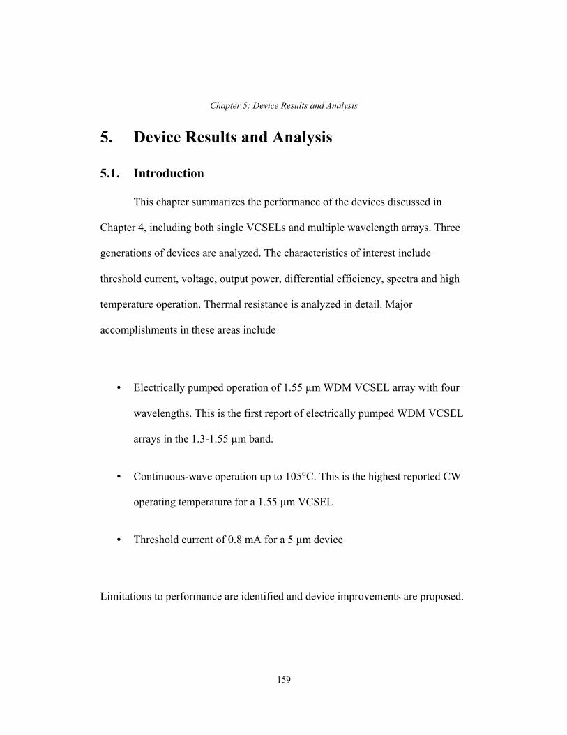
Chapter 5: Device Results and Analysis
5. Device Results and Analysis
5.1. Introduction
This chapter summarizes the performance of the devices discussed in
Chapter 4, including both single VCSELs and multiple wavelength arrays. Three
generations of devices are analyzed. The characteristics of interest include
threshold current, voltage, output power, differential efficiency, spectra and high
temperature operation. Thermal resistance is analyzed in detail. Major
accomplishments in these areas include
• Electrically pumped operation of 1.55 µm WDM VCSEL array with four
wavelengths. This is the first report of electrically pumped WDM VCSEL
arrays in the 1.3-1.55 µm band.
• Continuous-wave operation up to 105°C. This is the highest reported CW
operating temperature for a 1.55 µm VCSEL
• Threshold current of 0.8 mA for a 5 µm device
Limitations to performance are identified and device improvements are proposed.
159

Chapter 5: Device Results and Analysis
5.2. Generation A: 85°C continuous wave operation
The devices discussed in this section were fabricated with a single
wavelength active region containing 6 quantum wells and capped with a four
period superlattice. The top mirror was a 25.5 period p-GaAs/Al0.9Ga0.1As DBR
with an oxide aperture and a center wavelength of 1535 nm. The bottom mirror
was a 31 period non-intentionally doped GaAs/AlAs DBR with a center
wavelength of 1540 nm. The n-InP bondpad etch for reduced capacitance
described in Section 4.8.4 was omitted in this generation of devices. Device size
was determined by the depth of the oxide aperture. The VCSEL structure is
shown in Figure 5.1. The cavity standing wave pattern and refractive index profile
are shown in Figure 5.2.
p-GaAs/Al0.9Ga0.1As DBR
p-i-n InP/InGaAsP MQW/InP
nid GaAs/AlAs DBR
semi-insulating GaAs substrate
p-contactoxide aperture
n-contact
top-emitting
Si3N4 passivation
p-GaAs/Al0.9Ga0.1As DBR
p-i-n InP/InGaAsP MQW/InP
nid GaAs/AlAs DBR
semi-insulating GaAs substrate
p-contactoxide aperture
n-contact
top-emitting
Si3N4 passivation
Figure 5.1 Generation A VCSEL device structure
160
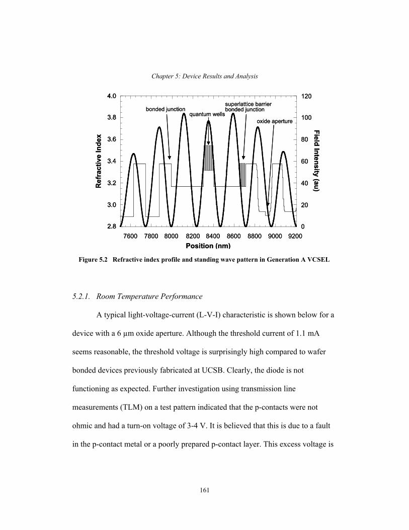
Chapter 5: Device Results and Analysis
4.0
3.8
3.6
3.4
3.2
3.0
2.8
120
100
80
60
40
20
0
Ref
ract
ive
Inde
xField Intensity (au)
7600 7800 8200 8400 8600 8800 90008000 9200Position (nm)
oxide aperture
superlattice barrier bonded junctionbonded junction
quantum wells
4.0
3.8
3.6
3.4
3.2
3.0
2.8
4.0
3.8
3.6
3.4
3.2
3.0
2.8
120
100
80
60
40
20
0
Ref
ract
ive
Inde
xField Intensity (au)
7600 7800 8200 8400 8600 8800 90008000 9200Position (nm)
oxide aperture
superlattice barrier bonded junctionbonded junction
quantum wells
Figure 5.2 Refractive index profile and standing wave pattern in Generation A VCSEL
5.2.1. Room Temperature Performance
A typical light-voltage-current (L-V-I) characteristic is shown below for a
device with a 6 µm oxide aperture. Although the threshold current of 1.1 mA
seems reasonable, the threshold voltage is surprisingly high compared to wafer
bonded devices previously fabricated at UCSB. Clearly, the diode is not
functioning as expected. Further investigation using transmission line
measurements (TLM) on a test pattern indicated that the p-contacts were not
ohmic and had a turn-on voltage of 3-4 V. It is believed that this is due to a fault
in the p-contact metal or a poorly prepared p-contact layer. This excess voltage is
161

Chapter 5: Device Results and Analysis
not related to the bonded junction. The high forward voltage does not impact
lasing on the optical time scale, but will contribute significantly to device self-
heating.
0
0.1
0.2
0.3
0.4
0.5
0
5
10
15
0 1 2 3 4 5 6 7 8 9 10
Out
put p
ower
(mW
)
Voltage (V)
Current (mA)
0
0.1
0.2
0.3
0.4
0.5
0
5
10
15
0 1 2 3 4 5 6 7 8 9 10
Out
put p
ower
(mW
)
Voltage (V)
Current (mA)
Figure 5.3 Room temperature (20°C) light-voltage-current characteristic of Generation A VCSEL with 6 µm aperture
The lasing spectrum for a 5 µm device at a bias current of 6 mA is shown
in Figure 5.4. The lasing wavelength at this bias level is 1529.6 nm. The side
mode suppression ratio (SMSR) is 45 dB. Single mode operation was observed
over a wide range of currents for device sizes up to 5 µm. Larger devices operated
with multiple modes.
162

Chapter 5: Device Results and Analysis
-90
-80
-70
-60
-50
-40
-30
-20
-10
1525 1526 1527 1528 1529 1530 1531 1532 1533
Wavelength (nm)
Log
pow
er (a
u)
SMSR = 45 dB
-90
-80
-70
-60
-50
-40
-30
-20
-10
1525 1526 1527 1528 1529 1530 1531 1532 1533
Wavelength (nm)
Log
pow
er (a
u)
SMSR = 45 dB
Figure 5.4 Single mode lasing spectrum from 5 µm device with SMSR = 45 dB
5.2.2. High Temperature Performance
Based on photoluminescence measurements, the room temperature gain
peak of the quantum well active region is estimated to be at 1544 nm. Both the
lasing wavelength and peak gain wavelength increase with temperature. The
lasing wavelength increases at a rate of 0.1 nm/°C, and the peak gain wavelength
increases at a rate of 0.5 nm/°C[1]. The shift in lasing wavelength was confirmed
during device testing, as illustrated in Figure 5.5.
163
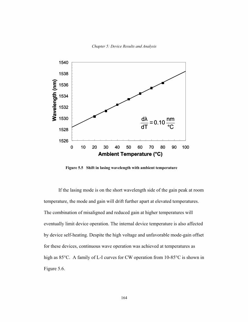
Chapter 5: Device Results and Analysis
1526
1528
1530
1532
1534
1536
1538
1540
0 10 20 30 40 50 60 70 80 90 100Ambient Temperature (°C)
Wav
elen
gth
(nm
)
Cnm 0.10
dTdλ
°=
1526
1528
1530
1532
1534
1536
1538
1540
0 10 20 30 40 50 60 70 80 90 100Ambient Temperature (°C)
Wav
elen
gth
(nm
)
Cnm 0.10
dTdλ
°=
Figure 5.5 Shift in lasing wavelength with ambient temperature
If the lasing mode is on the short wavelength side of the gain peak at room
temperature, the mode and gain will drift further apart at elevated temperatures.
The combination of misaligned and reduced gain at higher temperatures will
eventually limit device operation. The internal device temperature is also affected
by device self-heating. Despite the high voltage and unfavorable mode-gain offset
for these devices, continuous wave operation was achieved at temperatures as
high as 85°C. A family of L-I curves for CW operation from 10-85°C is shown in
Figure 5.6.
164

Chapter 5: Device Results and Analysis
0
0.1
0.2
0.3
0.4
0.5
0 1 2 3 4 5 6 7 8 9 1Current (mA)
Out
put P
ower
(mW
)
30°C
40°C
60°C
20°C
70°C
80°C
50°C
85°C
0
Figure 5.6 Continuous-wave L-I curves for ambient temperatures of 20-85°C
5.2.3. Thermal Resistance
The high temperature operation of these devices may be described using a
simple thermal model that includes both ambient temperature and device self-
heating. It is assumed that the device stops lasing once the active region reaches a
certain maximum temperature, Tmax. This bias point is referred to as rollover and
is illustrated below.
165
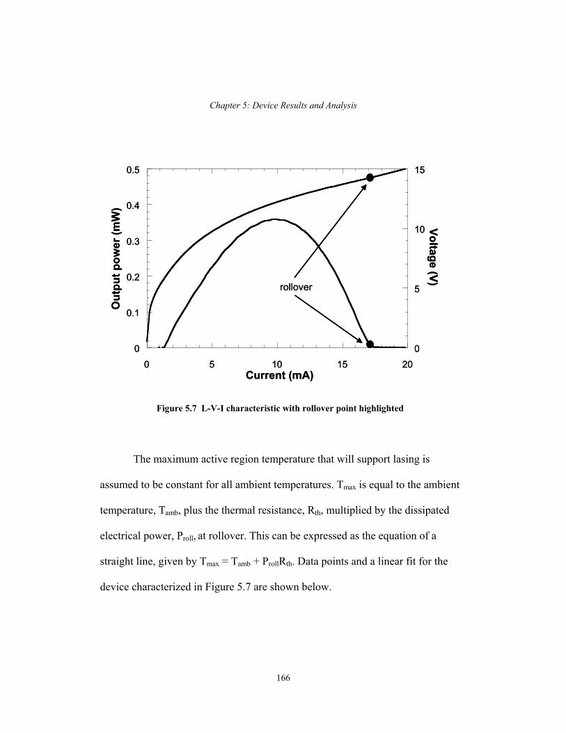
Chapter 5: Device Results and Analysis
0
0.1
0.2
0.3
0.4
0.5
0
5
10
15
0 5 10 15 20
Out
put p
ower
(mW
)Voltage (V)
Current (mA)
rollover
0
0.1
0.2
0.3
0.4
0.5
0
5
10
15
0 5 10 15 20
Out
put p
ower
(mW
)Voltage (V)
Current (mA)
rollover
Figure 5.7 L-V-I characteristic with rollover point highlighted
The maximum active region temperature that will support lasing is
assumed to be constant for all ambient temperatures. Tmax is equal to the ambient
temperature, Tamb, plus the thermal resistance, Rth, multiplied by the dissipated
electrical power, Proll, at rollover. This can be expressed as the equation of a
straight line, given by Tmax = Tamb + ProllRth. Data points and a linear fit for the
device characterized in Figure 5.7 are shown below.
166

Chapter 5: Device Results and Analysis
Threshold
Rollover
0
50
100
150
200
250
300
0 20 40 60 80 100 120
Ambient Temperature (°C)
Dis
sipa
ted
Elec
tric
al P
ower
(mW
)
Tmax = Tamb + ProllRth
Tmax = 120°CRth = 0.41°C/mW
Threshold
Rollover
0
50
100
150
200
250
300
0 20 40 60 80 100 120
Ambient Temperature (°C)
Dis
sipa
ted
Elec
tric
al P
ower
(mW
)
Tmax = Tamb + ProllRth
Tmax = 120°CRth = 0.41°C/mW
Figure 5.8 Dissipated electrical power and thermal resistance of 6 µm device in 46 µm pillar
The data points indicated by squares show the electrical power dissipated
at the bias point where the L-I characteristic has rolled over and the device is no
longer lasing. The data points indicated by circles show the electrical power
dissipated at threshold. The continuous-wave operating regime is bounded by the
threshold and rollover dissipated power curves. A thermal resistance of
0.41°C/mW is extracted from the linear fit for a device defined by a 46 µm
diameter pillar and 6 µm diameter oxide aperture. The maximum active region
167

Chapter 5: Device Results and Analysis
temperature that will support pulsed lasing is determined to be 120°C. The simple
fit used to extract these parameters treats the active region temperature as a one-
dimensional distribution. A higher degree of accuracy could be obtained by using
a two or three-dimensional model to determine local heating within the active
region.
The slope of the rollover dissipated power line is determined by the
thermal resistance of the device. The device design is already well-optimized for
high thermal conductivity. The measurements described in this chapter were made
after mounting the VCSEL chip on a temperature-controlled copper stage using a
thermally conductive paste. Devices were tested in a p-side up configuration
without additional special heat sinking. The thermal resistance could be reduced
slightly with an improved packaging scheme such as flip-chip bonding. However,
in order to maintain a cost advantage over edge-emitting lasers, it is desirable to
keep VCSEL device mounting as simple as possible. The x-intercept of the
dissipated power line corresponds to the maximum lasing temperature under
pulsed operation (no device self-heating). This maximum temperature can be
increased by providing higher material gain at elevated temperatures. Increased
gain above room temperature may be provided through improved quantum well
design or by switching to an active region material with superior high temperature
168

Chapter 5: Device Results and Analysis
gain characteristics, such as AlInGaAs. The gain available to the lasing mode is
determined by the peak material gain and the mode-gain offset. Proper alignment
of the mode position and gain peak would lead to increased modal gain and a
higher maximum lasing temperature. The bottom boundary of the continuous-
wave operating regime may be lowered by reducing the threshold current or
voltage. The effects of reducing threshold voltage will be seen in Generation B
devices.
The thermal resistance of the device can be used to determine the thermal
conductivity of the bottom DBR. The bottom DBR separates the heat source
(active region) from the heat sink (substrate and copper stage). For a disk source
on a large substrate, three-dimensional heat flow may be assumed. The thermal
resistance may be expressed as[2]:
dR
DBRth κ2
1=
Equation 5.1
where κDBR is the thermal conductivity of the bottom DBR and d is the pillar
diameter. Using the thermal resistance value calculated above, the thermal
conductivity of the bottom DBR is determined to be 0.263 W/cm K. This value is
only slightly lower than the expected value for GaAs and AlAs in parallel.
169

Chapter 5: Device Results and Analysis
Material Thermal conductivity (W/cm K) GaAs 0.44 AlAs 0.91 GaAs/AlAs DBR (calculated parallel) 0.297 GaAs/AlAs DBR (actual) 0.263
Table 5.1 Thermal conductivities of GaAs, AlAs and GaAs/AlAs DBR
This slight deviation is due to phonon scattering. A portion of the phonon
energy is scattered at each heterointerface, limiting heat transport in the transverse
direction. This effect limits thermal conductivity in all DBR structures containing
a large number of interfaces. Despite this reduction, the thermal conductivity of
GaAs/AlAs DBRs is still higher than that of other long wavelength DBRs
Knowing the thermal resistance of the device, the L-I characteristic may
be used to determine the internal device temperature as a function of bias current.
The temperature rise relative to the ambient temperature is given by the product
of bias current, bias voltage and thermal resistance. Output power and internal
device temperature are plotted in Figure 5.9 for the device with the L-I
characteristic shown in Figure 5.7.
170

Chapter 5: Device Results and Analysis
0
0.1
0.2
0.3
0.4
0.5
0
50
100
150
0 5 10 15 20
Out
put p
ower
(mW
)Internal device tem
perature (°C)
Current (mA)
0
0.1
0.2
0.3
0.4
0.5
0
50
100
150
0 5 10 15 20
Out
put p
ower
(mW
)Internal device tem
perature (°C)
Current (mA)
Figure 5.9 Output power and internal device temperature versus bias current at 20°C
It should be noted that superior thermal performance was achieved on a
large number of devices. Thirty-seven VCSELs of various sizes that passed
current were characterized over a range of temperatures. All of these devices had
maximum continuous-wave operating temperatures of 65°C or greater. This may
be taken as an indication of VCSEL consistency and quality across the entire
sample. A histogram of the maximum CW operating temperature is plotted in
Figure 5.10.
171
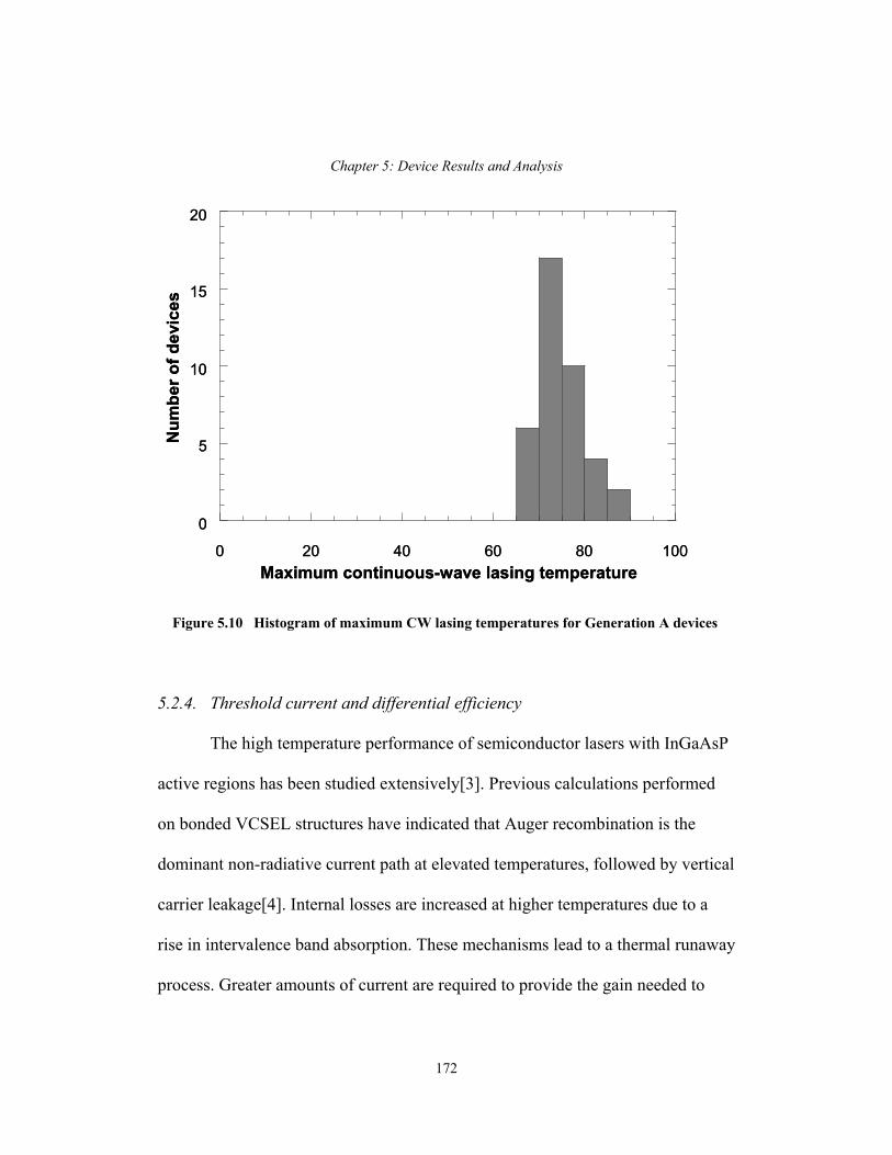
Chapter 5: Device Results and Analysis
0
5
10
15
20
0 20 40 60 80Maximum continuous-wave lasing temperature
Num
ber o
f dev
ices
0
5
10
15
20
0 20 40 60 80Maximum continuous-wave lasing temperature
Num
ber o
f dev
ices
100100
Figure 5.10 Histogram of maximum CW lasing temperatures for Generation A devices
5.2.4. Threshold current and differential efficiency
The high temperature performance of semiconductor lasers with InGaAsP
active regions has been studied extensively[3]. Previous calculations performed
on bonded VCSEL structures have indicated that Auger recombination is the
dominant non-radiative current path at elevated temperatures, followed by vertical
carrier leakage[4]. Internal losses are increased at higher temperatures due to a
rise in intervalence band absorption. These mechanisms lead to a thermal runaway
process. Greater amounts of current are required to provide the gain needed to
172

Chapter 5: Device Results and Analysis
compensate for an internal temperature increase. This additional injected current
further increases the temperature of the device, creating the need for even more
current. This process limits the differential efficiency and maximum output power
of the laser. The internal efficiency is reduced at higher temperatures by vertical
electron leakage. Due to a low effective mass and shallow conduction band
potential wells, injected electrons can easily overshoot the quantum well region or
escape before recombining radiatively. The threshold current is affected by the
same mechanisms. In Figure 5.11, the continuous-wave threshold current density
and differential efficiency are plotted as a function of ambient temperature for a 6
µm device. It should noted that the threshold current density is calculated based
on the diameter of the oxide aperture, although there may be significant current
speading beyond that point.
0
2
4
6
8
10
0
2
4
6
8
10
0 20 40 60 80 100Ambient temperature (°C)
Thre
shol
d C
urre
nt D
ensi
ty (k
A/c
m2 )
Differential Efficiency (%
)
0
2
4
6
8
10
0
2
4
6
8
10
0 20 40 60 80 100Ambient temperature (°C)
Thre
shol
d C
urre
nt D
ensi
ty (k
A/c
m2 )
Differential Efficiency (%
)
Figure 5.11 Continuous-wave threshold current density and differential efficiency versus ambient temperature for a device with a 6 µm oxide aperture
173
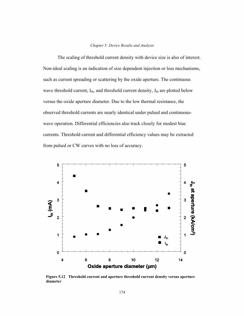
Chapter 5: Device Results and Analysis
The scaling of threshold current density with device size is also of interest.
Non-ideal scaling is an indication of size dependent injection or loss mechanisms,
such as current spreading or scattering by the oxide aperture. The continuous
wave threshold current, Ith, and threshold current density, Jth are plotted below
versus the oxide aperture diameter. Due to the low thermal resistance, the
observed threshold currents are nearly identical under pulsed and continuous-
wave operation. Differential efficiencies also track closely for modest bias
currents. Threshold current and differential efficiency values may be extracted
from pulsed or CW curves with no loss of accuracy.
0
1
2
3
4
5
0
1
2
3
4
5
4 6 8 10 12 14
Jth at aperture (kA
/cm2)
I th(m
A)
Oxide aperture diameter (µm)
Jth
Ith
0
1
2
3
4
5
0
1
2
3
4
5
4 6 8 10 12 14
Jth at aperture (kA
/cm2)
I th(m
A)
Oxide aperture diameter (µm)
0
1
2
3
4
5
0
1
2
3
4
5
4 6 8 10 12 14
Jth at aperture (kA
/cm2)
I th(m
A)
Oxide aperture diameter (µm)
Jth
Ith
Figure 5.12 Threshold current and aperture threshold current density versus aperturediameter174
Chapter 5: Device Results and Analysis
The data suggests a broad-area aperture threshold current density of 2.4
kA/cm2 for this generation of devices. The threshold current decreases
monotonically with device size until the aperture diameter reaches 7 µm. The
saturation of threshold current and sharp rise in threshold current density at that
point indicate the presence of a size-dependent loss mechanism. The diameter of 7
µm is too large for scattering losses to reach appreciable values. The increased
current spreading in bonded long wavelength VCSELs compared to short
wavelength VCSELs is due to a number of factors. The current confining aperture
in these wafer bonded VCSELs is more than 400 nm from the quantum well
region, compared to 50 nm or less in short wavelength VCSELs. The lack of a
robust aperturing technique on InP forces aperture placement in the
GaAs/AlGaAs DBR. The injected current must travel across the bonded junction
and p-InP cladding before reaching the active region, spreading in response to
electrical resistance. The bonded junction is highly resistive, as discussed in
Chapter 2. This forces current to spread laterally. The use of zinc as a p-type
dopant also influence electrical characteristics. Due to high p-type absorption
losses, a low doping level is chosen in the p-InP cladding. The high diffusivity of
zinc during the growth and bonding processes makes it essential to leave the 1000
Å of InP cladding nearest the quantum wells undoped to prevent damage to the
active region.
175
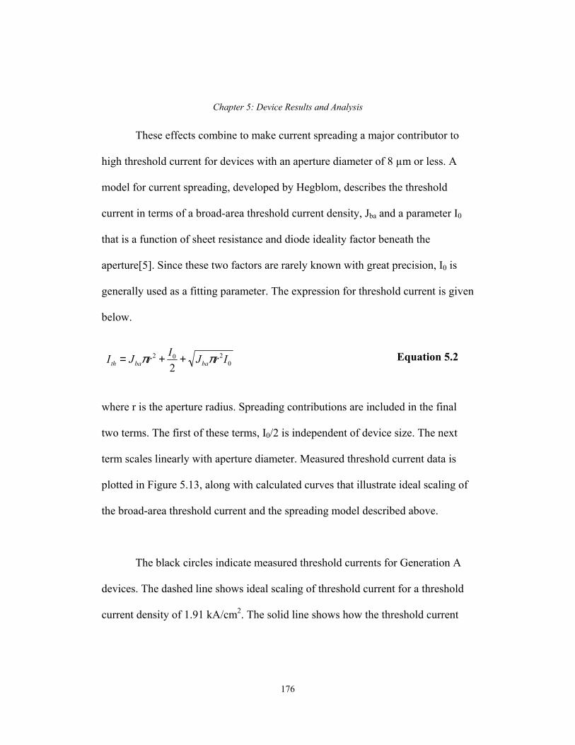
Chapter 5: Device Results and Analysis
These effects combine to make current spreading a major contributor to
high threshold current for devices with an aperture diameter of 8 µm or less. A
model for current spreading, developed by Hegblom, describes the threshold
current in terms of a broad-area threshold current density, Jba and a parameter I0
that is a function of sheet resistance and diode ideality factor beneath the
aperture[5]. Since these two factors are rarely known with great precision, I0 is
generally used as a fitting parameter. The expression for threshold current is given
below.
Equation 5.2 0
202
2IrJIrJI babath ππ ++=
where r is the aperture radius. Spreading contributions are included in the final
two terms. The first of these terms, I0/2 is independent of device size. The next
term scales linearly with aperture diameter. Measured threshold current data is
plotted in Figure 5.13, along with calculated curves that illustrate ideal scaling of
the broad-area threshold current and the spreading model described above.
The black circles indicate measured threshold currents for Generation A
devices. The dashed line shows ideal scaling of threshold current for a threshold
current density of 1.91 kA/cm2. The solid line shows how the threshold current
176

Chapter 5: Device Results and Analysis
177
0.1
1
10
1 1
Cur
rent
(mA
)
Aperture diameter (µm)20
Measured data
Jth = 1.91 kA/cm2
Jth = 1.91 kA/cm2 + current spreading
0.1
1
10
1 1
Cur
rent
(mA
)
Aperture diameter (µm)20
0.1
1
10
1 1
Cur
rent
(mA
)
Aperture diameter (µm)20
Measured dataMeasured data
Jth = 1.91 kA/cm2
Jth = 1.91 kA/cm2 + current spreading
Figure 5.13 Threshold current versus oxide aperture diameter
000
scales using the same broad area threshold current density and using the
expression above to include the effects of spreading beneath the aperture. This
analysis suggests that 20-40% of the measured threshold current was due to
current spreading, depending on aperture size. Although the solid line shows an
improved fit, the spreading model used does not appear to give a complete
description of threshold current for small devices. Previous analysis by Margalit,
including near-field imaging, attributed this effect to reduced mode-gain
overlap[6]. The small index perturbation of the oxide aperture does not effectively
Chapter 5: Device Results and Analysis
confine the mode at small diameters, reducing the transverse confinement factor
and increasing threshold. Additionally, current spreading at the bonded junction
may not be adequately described by the model above. Further discussion of
current spreading, including calculated profiles for the hole current density will be
presented in Section 5.3.
5.2.5. Summary
Electrically pumped, double bonded VCSELs with a lasing wavelength of
1528 nm were fabricated. The maximum CW operating temperature achieved was
85°C. At the time, this was the highest CW operating temperature reported for an
electrically pumped long wavelength VCSEL. All devices lased under CW
operation at temperatures up to 65°C. The maximum output power at 20°C was
0.55 mW. Previously fabricated devices without a superlattice barrier had a
maximum CW operating temperature of 74°C and a maximum output power of
0.5 mW at 20°C[7]. Performance improvements relative to previous bonded
VCSELs fabricated at UCSB are attributed to reduced loss in the p-mirror and
fewer non-radiative recombination centers in the bonded active region. The
maximum output power at 70°C was 62 µW. Threshold currents of 0.9 mA were
obtained for a 6 µm aperture. The lowest aperture threshold current density
measured was 1.9 kA/cm2 for an 13 µm aperture. Performance improvements are
178

Chapter 5: Device Results and Analysis
expected for devices with a more favorable mode-gain offset, lower turn-on
voltage and reduced series resistance.
5.3. Generation B: Multiple wavelength arrays, 105°C continuous wave operation
The high temperature performance of Generation A VCSELs was limited
by device self-heating. Analysis of the thermal resistance suggested that
continuous-wave operation at temperatures over 100°C would be possible if the
threshold voltage could be reduced to 3 V. As the high diode voltage and
resistance were attributed to poor metallization, this goal is certainly within reach.
An additional goal in this generation of devices is the fabrication of multiple
wavelength arrays using the intracavity superlattice tuning layer described in
Chapters 3 and 4. Prior to bonding, single layers of InP or InGaAsP were
selectively etched on a 250 µm pitch to define ∆λ ≈ 5 nm between adjacent
devices, as shown in Figure 5.14. This pattern was repeated over the entire
sample. Reasonably uniform performance is expected over the tuning range of 15
nm as discussed in Chapter 4.
179

Chapter 5: Device Results and Analysis
InP substrate
InGaAsP etch stop
n-InP cladding
InGaAsP MQW
p-InP cladding
superlattice
λ4 λ3 λ2 λ1
4X 75Å InP/75Å 1.3Q
InP substrate
InGaAsP etch stop
n-InP cladding
InGaAsP MQW
p-InP cladding
superlattice
λ4 λ3 λ2 λ1
4X 75Å InP/75Å 1.3Q
The same epitaxial material was used in the fabrication of Generation B
devices as was used in Generation A devices. The actual device structure was
nearly identical. A slightly different mask set was used, with pillar dimensions
and bondpad layout varying from the Generation A design. Other than variation
with size, these changes are not expected to affect DC device performance. It is
expected that the superlattice layer will not only provide 5 nm wavelength tuning
between devices, but that the uneteched superlattice periods will preserve active
region quality as described in Chapter 3.
Figure 5.14 Patterned intracavity superlattice for multiple wavelength cavity definition
180

Chapter 5: Device Results and Analysis
5.3.1. Room Temperature Performance
A light-voltage-current (L-V-I) characteristic is shown below for a device
with a 44 µm pillar and 7 µm oxide aperture. The threshold current of 1.0 mA is
similar to the values observed for Generation A devices. However, the threshold
voltage has been sharply reduced. A 7 µm device from Generation A had a
threshold voltage of 6.6 V and a series resistance of 430 Ω. A Generation B
device with the same aperture dimension has a threshold voltage of 2.5 V and a
series resistance of 325 Ω. This voltage reduction is due to an improved p-contact.
The reduced device self-heating manifests itself in higher peak output power and
is expected to improve high temperature performance as well.
0
0.1
0.2
0.3
0.4
0.5
0.6
0.7
0
1
2
3
4
5
6
7
0 2 4 6 8 10 12
Out
put P
ower
(mW
)Voltage (V)
Current (mA)
0
0.1
0.2
0.3
0.4
0.5
0.6
0.7
0
1
2
3
4
5
6
7
0 2 4 6 8 10 12
Out
put P
ower
(mW
)Voltage (V)
Current (mA)
Figure 5.15 Room temperature (20°C) L-V-I characteristic of Generation B VCSEL with aperture diameter of 7 µm
181

Chapter 5: Device Results and Analysis
Light-current characteristics are shown in Figure 5.16 for four adjacent 5
µm devices. Threshold currents are nearly uniform across the array, varying
between 1.04 and 1.10 mA. This is well within the limits expected based on
earlier calculations. The slight variations in threshold and differential efficiency
can be attributed to the different mode-gain-reflectivity offsets of the channels, as
discussed in Chapter 4. Channel 1 refers to the device with the shortest
wavelength and Channel 4 refers to the device with the longest wavelength.
0
0.1
0.2
0.3
0.4
0.5
0 2 4 6 8 10
Channel 1Channel 2Channel 3Channel 4
Out
put P
ower
(mW
)
Current (mA)Figure 5.16 L-I characteristics for four adjacent 5 µm devices in WDM VCSEL array
12
182

Chapter 5: Device Results and Analysis
Uniformity in threshold voltage and series resistance is also desirable, so
that the same power supply may be used to drive each element in the array.
Similar electrical characteristics would also ensure similar thermal performance,
encompassing both peak output powers and operation at high ambient
temperatures. Voltage-current characteristics for the VCSEL array above are
shown in Figure 5.17.
0
1
2
3
4
5
6
7
0 2 4 6 8 10
Channel 1Channel 2Channel 3Channel 4
Volta
ge (V
)
Current (mA)Figure 5.17 V-I characteristics for four adjacent 5 µm devices in WDM VCSEL array
12
The theoretical effects of patterned bonding on diode characteristics are
difficult to estimate. In practice, similar voltage-current characteristics were
183

Chapter 5: Device Results and Analysis
measured across a number of VCSEL arrays. No systematic voltage dependence
on channel number was observed. For the array with the characteristics shown
above, the diode turn-on voltage varied between 1.7 and 2.0 V, as determined by
the intercept of the linear portion of the diode characteristic with the y-axis. The
threshold voltage was between 2.2 and 2.6 V. The series resistance varied
between 283 and 333 Ω.
Lasing spectra at a bias of 6 mA are shown in Figure 5.18 for the WDM
VCSEL array. The lasing wavelengths are 1509.1 nm, 1513.8 nm, 1518.6 nm, and
1524.4 nm. The active region photoluminescence peak is at 1542 nm and the
output DBR reflectivity peak is at 1535 nm. All four channels are on the short
wavelength side of the gain and reflectivity peaks. The higher numbered channels
are located at longer wavelengths and are expected to have lower threshold
currents and lower differential efficiencies, balancing device performance. The
exact wavelengths depend on the thickness of the tuning layers. Increased control
over the channel spacing is expected with improved superlattice growth and etch
conditions.
184

Chapter 5: Device Results and Analysis
-50
-45
-40
-35
-30
-25
-20
-15
1500 1505 1510 1515 1520 1525 1530 1535
Wavelength (nm)
Log
pow
er (a
u)
λ1 λ2 λ3 λ4
-50
-45
-40
-35
-30
-25
-20
-15
1500 1505 1510 1515 1520 1525 1530 1535
Wavelength (nm)
Log
pow
er (a
u)
λ1 λ2 λ3 λ4
Figure 5.18 Lasing spectra for four adjacent 5 µm devices in WDM VCSEL array
Characteristics for the WDM VCSEL array with an aperture diameter of 5
µm are summarized in the table below.
Channel # λ (nm) Ith (mA) Vth (V) Rs (Ω) Peak output (mW) 1 1509.1 1.10 2.77 333 0.443 2 1513.8 1.08 2.40 283 0.429 3 1518.6 1.08 2.31 299 0.390 4 1524.4 1.07 2.52 310 0.431
Table 5.2 Summary of WDM VCSEL array results for 5 µm aperture diameter185

Chapter 5: Device Results and Analysis
The lowered threshold voltage and series resistance indicate that high
temperature operation beyond 85°C should be possible with this generation of
devices. Since the same epitaxial material was used, the VCSEL thermal
conductivity of the structure should be identical to that of previously fabricated
devices. It follows that the thermal resistance should also remain unchanged for
devices with the same pillar size. A family of L-I curves for continuous-wave
operation from 20-105°C is shown in Figure 5.19. The room-temperature L-V-I
characteristic of this VCSEL is shown in Figure 5.20. This device was channel 4
in a WDM array and had a lasing wavelength of 1526 nm.
0
0.1
0.2
0.3
0.4
0.5
0.6
0.7
0 1 2 3 4 5 6 7 8 9 10 11 1
Current (mA)
Out
put P
ower
(mW
) 40°C
50°C
60°C
70°C
80°C
90°C
100°C
105°C
30°C
20°C
0
0.1
0.2
0.3
0.4
0.5
0.6
0.7
0 1 2 3 4 5 6 7 8 9 10 11 1
Current (mA)
Out
put P
ower
(mW
) 40°C
50°C
60°C
70°C
80°C
90°C
100°C
105°C
30°C
20°C
22
Figure 5.19 Continuous-wave L-I curves for ambient temperatures of 20-105°C
186

Chapter 5: Device Results and Analysis
It should be noted that the mode-gain offset is in fact slightly larger for
this generation of devices, even for the longest array wavelength. The improved
high temperature performance relative to previously fabricated devices is due to
reduced diode turn-on voltage and lowered differential resistance.
5.3.2. Thermal Resistance
The thermal resistance of these devices can be analyzed using the
technique described in Section 5.2.3. Devices with 6 µm apertures in 46 µm
pillars from each of the generations are compared. The results are plotted in
Figure 5.20.
0
50
100
150
200
250
300
0 20 40 60 80 100 120Ambient Temperature (°C)
Dis
sipa
ted
Elec
tric
al P
ower
(mW
)
Rollover
Generation A, 85°C max, threshold Generation B, 105°C max, threshold
Tmax = Tamb + PdisRth
Tmax = 120°CRth = 0.41°C/mW
0
50
100
150
200
250
300
0 20 40 60 80 100 120Ambient Temperature (°C)
Dis
sipa
ted
Elec
tric
al P
ower
(mW
)
Rollover
Generation A, 85°C max, threshold Generation B, 105°C max, threshold
Tmax = Tamb + PdisRth
Tmax = 120°CRth = 0.41°C/mW
0
50
100
150
200
250
300
0 20 40 60 80 100 120Ambient Temperature (°C)
Dis
sipa
ted
Elec
tric
al P
ower
(mW
)
Rollover
Generation A, 85°C max, threshold Generation B, 105°C max, threshold
Tmax = Tamb + PdisRth
Tmax = 120°CRth = 0.41°C/mW
Figure 5.20 Thermal resistance and maximum operating temperature for Generation A and Generation B VCSELs with identical dimensions.
187

Chapter 5: Device Results and Analysis
As expected, the dissipated electrical power at rollover for the Generation
B device at temperature above 85°C falls along the same line established by the
Generation A device. Since the devices have the same active region and thermal
conductivity, the same amount of dissipated power will cause identical heating in
the active region. The difference between the two generations lies in the amount
of power required to reach threshold. The reduced threshold voltage of Generation
B devices opens a larger window between the threshold and rollover power
curves, enabling continuous-wave operation at temperatures up to 105°C. The
shaded area shows the increased range of ambient temperatures and dissipated
electrical powers over which Generation B devices are capable of operating. For
identical device dimensions, the two generations of devices have the same thermal
resistance of 0.41°C/mW, indicating a bottom DBR thermal conductivity of 0.263
W/cm K.
The thermal resistance increases with decreasing pillar diameter, as heat
must flow through a smaller area to the copper stage. The thermal conductivity of
the bottom DBR may be extracted or confirmed by observing the variation of
thermal resistance with pillar diameter, according to the expression
dR
DBRth κ2
1= Equation 5.3
188

Chapter 5: Device Results and Analysis
where Rth is the device thermal resistance, κDBR is the thermal conductivity of the
bottom DBR and d is the pillar diameter. The linear fit technique described in
Section 5.2.3 was used to determine thermal resistance for pillar diameters of 44-
52 µm. These results are plotted below, including a curve fit using κDBR = 0.263
W/cm K.
300
320
340
360
380
400
420
440
460
43 44 45 46 47 48 49 50 51 52 53
Pillar diameter (µm)
Ther
mal
resi
stan
ce (K
/W)
ddR
DBRth
1W
K cm 901.12
1 ==κ
K cmW 263.0=DBRκ
300
320
340
360
380
400
420
440
460
43 44 45 46 47 48 49 50 51 52 53
Pillar diameter (µm)
Ther
mal
resi
stan
ce (K
/W)
ddR
DBRth
1W
K cm 901.12
1 ==κ
K cmW 263.0=DBRκ
r
The ther
described with
the values extra
generations.
Figure 5.21 Thermal resistance versus pillar diamete
mal resistance scales with a 1/d dependence that is suitably
κDBR = 0.263 W/cm K. This provides additional confirmation of
cted using single device sizes from each of the two VCSEL
189

Chapter 5: Device Results and Analysis
5.3.3. Threshold Current and Differential Efficiency
The threshold current density and differential efficiency for a 6 µm device
are plotted below over a range of temperatures.
0
2
4
6
8
10
12
14
16
0
2
4
6
8
10
12
14
16
0 20 40 60 80 100 120Temperature (°C)
Thre
shol
d C
urre
nt D
ensi
ty (k
A/c
m2 )
Differential Efficiency (%
)
0
2
4
6
8
10
12
14
16
0
2
4
6
8
10
12
14
16
0 20 40 60 80 100 120Temperature (°C)
Thre
shol
d C
urre
nt D
ensi
ty (k
A/c
m2 )
Differential Efficiency (%
)
kA/cm
20°C)
efficie
highly
the p-I
Figure 5.22 CW threshold current density and differential efficiency versus ambient temperature
Threshold current levels were slightly lower (2.5 kA/cm2 versus 2.8
2 at 20°C) and differential efficiencies slightly higher (15% versus 9% at
in this generation of devices. This indicates an increase in internal quantum
ncy, ηi, or a reduction of internal loss, αi. Long wavelength VCSELs are
sensitive to absorption in p-type material. The zinc concentration profile in
nP cladding is difficult to manage precisely during the growth and bonding
190
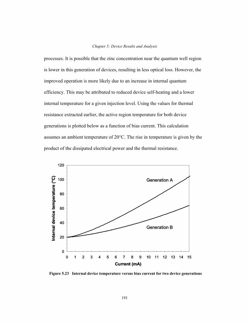
Chapter 5: Device Results and Analysis
processes. It is possible that the zinc concentration near the quantum well region
is lower in this generation of devices, resulting in less optical loss. However, the
improved operation is more likely due to an increase in internal quantum
efficiency. This may be attributed to reduced device self-heating and a lower
internal temperature for a given injection level. Using the values for thermal
resistance extracted earlier, the active region temperature for both device
generations is plotted below as a function of bias current. This calculation
assumes an ambient temperature of 20°C. The rise in temperature is given by the
product of the dissipated electrical power and the thermal resistance.
0
20
40
60
80
100
120
0 1 2 3 4 5 6 7 8 9 10 11 12 13 14 15
Current (mA)
Inte
rnal
dev
ice
tem
pera
ture
(°C
)
Generation A
Generation B
0
20
40
60
80
100
120
0 1 2 3 4 5 6 7 8 9 10 11 12 13 14 15
Current (mA)
Inte
rnal
dev
ice
tem
pera
ture
(°C
)
Generation A
Generation B
Figure 5.23 Internal device temperature versus bias current for two device generations
191

Chapter 5: Device Results and Analysis
This plot reveals the striking difference in device self-heating between the
two generations. At a bias current of 1 mA, near threshold, the device
temperatures differ by 2°C. This increase has only a minor effect on the material
gain and only a small difference in threshold current density is observed.
Temperature dependent loss mechanisms remain unaffected at these relatively
low temperatures. However, at higher bias currents, Generation B devices operate
with a much lower internal temperature. At 10 and 15 mA drive currents, the
temperature differences are 26°C and 40°C, respectively. InGaAsP lasers are
particularly sensitive to temperature dependent loss and leakage mechanisms,
including electron overshoot, Auger recombination and intervalence band
absorption. The reduced internal temperature dramatically improves laser
performance of Generation B devices relative to those of Generation A. Above
threshold, the reduced temperature is responsible for increased internal quantum
efficiency, lower internal loss, increased differential efficiency and higher peak
powers. The dissipated power could be reduced further by lowering the device
resistance. This could be accomplished by using larger pillars, or tunnel junction
injection with n-type DBRs.
The effects of current spreading beneath the oxide aperture were analyzed
in Section 5.2.4 using an analytically derived formula. These results indicated that
192

Chapter 5: Device Results and Analysis
20-40% of the observed threshold current was due to current spreading beneath
the aperture, depending on device size. No additional effort was made to reduce
current spreading in Generation B devices and similar scaling was observed.
Current injection into the VCSEL active region was simulated using a three-
dimensional software package to calculate local hole current densities. The
current profiles versus radius are plotted in Figures 5.24 and 5.25 for bias currents
of 1.5 mA and 10 mA. The oxide aperture radius is taken as 2.5 µm. The hole
current profile is calculated at the oxide aperture and at the first barrier in the
quantum well active region. The distance from the aperture to the barrier includes
128 nm of p-GaAs, the bonded junction and 310 nm of p-InP. The threshold
current is 1.0 mA.
0
5
10
15
20
25
30
0 1 2 3 4 5
aperturefirst barrier
Loca
l Hol
e C
urre
nt D
ensi
ty (k
A/c
m2 )
Radius (µm)
1.5 mA bias
0
25
50
75
100
125
150
0 1 2 3 4 5
aperturefirst barrier
Radius (µm)
10 mA bias
0
5
10
15
20
25
30
0 1 2 3 4 5
aperturefirst barrier
Loca
l Hol
e C
urre
nt D
ensi
ty (k
A/c
m2 )
Radius (µm)
1.5 mA bias
0
25
50
75
100
125
150
0 1 2 3 4 5
aperturefirst barrier
Radius (µm)
10 mA bias
Figures 5.24, 5.25 Local hole current density versus radius at oxide aperture and first barrier for bias currents of 1.5 and 10 mA
193
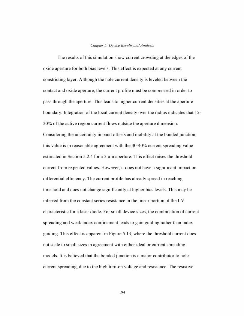
Chapter 5: Device Results and Analysis
The results of this simulation show current crowding at the edges of the
oxide aperture for both bias levels. This effect is expected at any current
constricting layer. Although the hole current density is leveled between the
contact and oxide aperture, the current profile must be compressed in order to
pass through the aperture. This leads to higher current densities at the aperture
boundary. Integration of the local current density over the radius indicates that 15-
20% of the active region current flows outside the aperture dimension.
Considering the uncertainty in band offsets and mobility at the bonded junction,
this value is in reasonable agreement with the 30-40% current spreading value
estimated in Section 5.2.4 for a 5 µm aperture. This effect raises the threshold
current from expected values. However, it does not have a significant impact on
differential efficiency. The current profile has already spread in reaching
threshold and does not change significantly at higher bias levels. This may be
inferred from the constant series resistance in the linear portion of the I-V
characteristic for a laser diode. For small device sizes, the combination of current
spreading and weak index confinement leads to gain guiding rather than index
guiding. This effect is apparent in Figure 5.13, where the threshold current does
not scale to small sizes in agreement with either ideal or current spreading
models. It is believed that the bonded junction is a major contributor to hole
current spreading, due to the high turn-on voltage and resistance. The resistive
194

Chapter 5: Device Results and Analysis
superlattice barrier in these devices also promotes current spreading. Device
efficiency would benefit greatly from an aperture placed in closer proximity to the
active region. Although apertures on InP are neither as simple nor as robust as
those on GaAs, it may possible for high-quality apertures to be defined using
selective wet etches[8] or the lateral oxidation of aluminum containing
compounds[9].
5.3.4. Summary
Four-channel WDM VCSEL arrays were fabricated. The wavelength span
is 1509.1 nm to 1524.4 nm with a channel spacing of approximately 5 nm. This is
the first independently addressable, multiple wavelength 1.55 µm VCSEL array.
Threshold currents and other device parameters were similar to those of single-
wavelength VCSELs. The maximum CW operating temperature achieved was
105°C. This is the highest CW operating temperature reported for a 1.55 µm
VCSEL. The maximum output power at 20°C was 0.65 mW. The maximum
output power at 80°C was 0.22 mW. Threshold currents of 0.8 mA were obtained
for a 5 µm device. The lowest threshold current density measured was 1.7 kA/cm2
for an 11 µm device. The improvement in high-temperature performance relative
to Generation A is due to a reduction in p-contact resistance.
195

Chapter 5: Device Results and Analysis
5.4. Crosstalk
Integration of multiple wavelength VCSELs on a single substrate enables
increased functionality at lower cost. However, the effects of simultaneously
operating individual VCSELs must be considered when evaluating array
suitability for use in an optical transmission system. The simultaneous operation
of array elements creates a situation in which the operating parameters of each
VCSEL, including carrier density and temperature, are affected by changes in
neighboring VCSELs. In this section, crosstalk between VCSEL array
components is considered in detail. Optical and thermal crosstalk mechanisms are
discussed and experimental results are used to validate device models. It is
observed that the large distance between devices minimizes these forms of
crosstalk.
5.4.1. Optical crosstalk
Optical crosstalk in VCSEL arrays has been considered by other
authors[10]. For devices on a common substrate, the primary concern is that
spontaneous emission from one device may generate carriers in an adjacent
device. In effect, this would “pre-bias” the second laser without current injection.
196

Chapter 5: Device Results and Analysis
1 2
h+e-
stimulated emission
Si3N4
top DBR
bottom DBR
active region
1 2
h+e-
stimulated emission
Si3N4
top DBR
bottom DBR
active region
It should be noted that this form of crosstalk depends only on spontaneous
emission, not stimulated emission. The lasing mode is well-guided by the DBRs
and index aperture, resulting in a narrow output beam normal to the substrate.
Only spontaneous emission occurs over a broad angular spectrum. A further
limitation is imposed by the bandgap energies of the semiconductor materials
used to fabricate these long wavelength VCSELs. Spontaneous emission for 1.55
µm diode lasers can be reasonably assumed to occur only at wavelengths greater
Figure 5.26 Optical crosstalk between two VCSELs resulting in carrier generation
197

Chapter 5: Device Results and Analysis
than 1.50 µm. This light will not be absorbed by semiconductors with a bandgap
energy greater than 0.83 eV. The GaAs DBR layers (Eg = 1.42 eV), Al0.9Ga 0.1As
DBR layers (Eg = 2.08 eV) and InP cladding (Eg = 1.35 eV) all have bandgap
energies far beyond this cutoff. Consequently, there will be no generation of
electron-hole pairs in these areas of the device. Spontaneous emission will only be
absorbed in the quantum well active region.
A simple model may be used to estimate the increase in carrier density
caused by optical crosstalk. Assume that a certain spontaneous emission power,
Ps, is emitted from the active region of VCSEL 1 in a narrow angular spectrum
along the common MQW active region toward VCSEL 2. As discussed earlier,
emission in other directions will not result in photo-generated carriers. For the
sake of simplicity, it is assumed that no diffraction or scattering takes place as the
spontaneous emission propagates toward the active region of VCSEL 2. This
propagation path is treated as a waveguide with an effective absorption coefficient
of α12. For the VCSEL structures in this work, this path includes active regions,
Si3N4 passivation layers, and free space. These assumptions clearly overstate the
magnitude of the optical crosstalk. However, the purpose of these calculations is
merely to estimate and provide an upper bound on the number of carriers
generated in VCSEL 2. If the distance between active regions is given by L, then
198

Chapter 5: Device Results and Analysis
the spontaneous emission power arriving at the active region of VCSEL 2 from
VCSEL 1, P21 is given by
Equation 5.4 LsePP 12
21α−=
This arriving power is now partially absorbed by the active region of
VCSEL 2. The absorption length in this device is given by d. The absorption
coefficient is written as αMQW. The spontaneous emission power from VCSEL 1
absorbed in the active region of VCSEL 2 is given by
( )DLs
MQWeePP αα −− −= 11212 Equation 5.5
This absorption generates carriers in the active region of VCSEL 2.
Assuming that each absorbed photon generates an electron hole pair, the carrier
generation rate is written as
VEP
dtdN
pgen
12= Equation 5.6
199
Chapter 5: Device Results and Analysis
where Ep is the photon energy and V is the active region volume and N is the
carrier density. Assuming that VCSEL 2 is biased below threshold (no stimulated
emission) and that there is no coupling between the electron and photon densities
in VCSEL 2, the carrier recombination rate is given by
τN
dtdN
rec
= Equation 5.7
where τ is the carrier lifetime. Under steady-state condition, the generation and
recombination rates are equal. The steady-state carrier density in the active
region of VCSEL 2 is
VEPN
p
τ12= Equation 5.8
Reasonable values for τ, Ep and V are 1 ns, 0.8 eV, and 7.85 µm3. The
active region volume is calculated using a thickness of 0.1 µm and a radius of 5
µm. The photon energy given corresponds to an emission wavelength of 1.55 µm.
P12 may also be estimated by inserting device parameters. The active region
radius of 5 µm corresponds to an absorption length, D, of 10 µm with an
absorption coefficient, αMQW, of 50 cm-1. The distance between active regions, L,
is 250 µm. The majority of this distance is in air and may be considered lossless.
200

Chapter 5: Device Results and Analysis
The silicon nitride layer also has a negligible loss coefficient. The only loss
between devices is between the active region centers and the device sidewall.
Assuming a pillar diameter of 50 µm, this distance is 40 µm for two devices and
has a loss coefficient of 50 cm-1. Based on off-axis detection of the spontaneous
emission power, a maximum value of 0.1 mW is assumed for Ps. Since this value
was estimated using a broad-area detector, the estimate may be as much as an
order of magnitude higher than the actual value. However, it should still be useful
in estimating an upper bound for the induced carrier density in VCSEL 2. The
parameters used to calculate the carrier density are summarized in Table 5.3.
Parameter Value Ps 0.1 mW α12 50 cm-1 L 40 µm αMQW 50 cm-1 D 10 µm Ep 0.8 eV V 7.85 µm3 τ 1 ns
Table 5.3 Parameters and values used in optical crosstalk calculations
201

Chapter 5: Device Results and Analysis
Using the values given above, it is determined that P12 = 3.99 µW and that
N = 3.97 x 1016 cm-3. This carrier density value may be used to extract an
equivalent injected current density. For electrical injection below threshold, the
carrier density may be written as
Equation 5.9 qdJN i τη=
where ηi is the internal quantum efficiency, J is the terminal current density, τ is
the carrier lifetime, q is the fundamental electronic charge and d is the active
region thickness. Rewriting this expression in terms of J, the terminal current
density is given by
τη i
NqdJ = Equation 5.10
The active region thickness, d, is 0.1 µm and the internal quantum
efficiency is approximately 0.8. The calculated carrier density induced in VCSEL
2 by spontaneous emission from VCSEL 1 is equivalent to an injection current
density of 0.079 kA/cm2. This is approximately 0.4% of the broad area threshold
current density of 1.9 kA/cm2. Despite the large value used for Ps, the calculated
equivalent crosstalk current density barely exceeds measurement resolution. In
202

Chapter 5: Device Results and Analysis
practice, the crosstalk power is much lower than this calculated value due to the
exceptionally narrow angular spectrum of spontaneous emission that can produce
carriers in adjacent devices. Diffraction, reflection and scattering losses are also
significant along the crosstalk propagation path. No meaningful difference in
threshold current was measured under pulsed operation between devices operated
individually and devices operated with their nearest neighbor biased above
threshold. The low optical crosstalk is attributed to wide pillar diameters, oxide-
confined active regions and low spontaneous emission photon energy. This value
could be reduced even further by depositing an absorptive film between devices
and by improving the active region carrier clamping efficiency above threshold.
However, no process improvements are required unless the device spacing is
dramatically reduced.
5.4.2. Thermal Crosstalk
In sections 5.2 and 5.3, the mechanism and effects of device self-heating
were considered. This treatment is appropriate when considering the operation of
an individual device. However, the thermal effects of multiple device operation
become relevant when discussing array operation. In long wavelength VCSEL
arrays, thermal crosstalk is even more significant due to the temperature
sensitivity of the active region.
203
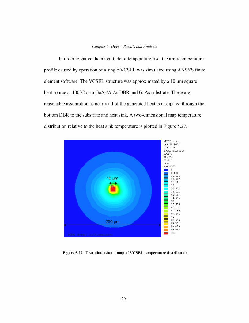
Chapter 5: Device Results and Analysis
In order to gauge the magnitude of temperature rise, the array temperature
profile caused by operation of a single VCSEL was simulated using ANSYS finite
element software. The VCSEL structure was approximated by a 10 µm square
heat source at 100°C on a GaAs/AlAs DBR and GaAs substrate. These are
reasonable assumption as nearly all of the generated heat is dissipated through the
bottom DBR to the substrate and heat sink. A two-dimensional map temperature
distribution relative to the heat sink temperature is plotted in Figure 5.27.
10 µm
250 µm
10 µm
250 µm
Figure 5.27 Two-dimensional map of VCSEL temperature distribution
204

Chapter 5: Device Results and Analysis
The simulation indicates that the temperature rise caused by VCSEL
operation is confined to a small area. At a distance of 250 µm, equal to the device
pitch, the temperature rise is only 0.5°C. Simulation results were tested
experimentally by biasing the laser above threshold and using a thermal
microprobe to measure surface temperature at different distances from the heat
source. These experimental results are plotted in Figure 5.28, along with a one-
dimensional profile of the map in Figure 5.27.
0
10
20
30
40
50
60
70
80
90
100
0 50 100 150 200 250 300
Distance (µm)
Act
ive
Reg
ion
Tem
pera
ture
Ris
e (°
C)
Measurement (normalized to simulation)
Simulation
0
10
20
30
40
50
60
70
80
90
100
0 50 100 150 200 250 300
Distance (µm)
Act
ive
Reg
ion
Tem
pera
ture
Ris
e (°
C)
Measurement (normalized to simulation)
Simulation
Figure 5.28 Comparision of thermal simulation and microprobe measurements
The two curves agree remarkably well. The difference in saturation
temperature is due to the difference in heat sink conditions between theory and
205
Chapter 5: Device Results and Analysis
experiment. In the simulation, an ideal heat sink was assumed. In practice, the
heat sink under the substrate had finite thermal conductivity. The saturation value
is also affected by pillar diameter, not included in the simulation.
The thermal crosstalk between array elements is measured by operating
VCSEL 1 at a fixed current and voltage while varying the electrical power
dissipated by VCSEL 2. The thermal isolation between VCSELs 1 and 2 is
defined as[11]:
1
212 T
PZ
∆
∆= Equation 5.11
where ∆P2 is the change in dissipated power of VCSEL 2 and ∆T1 is the
corresponding change in temperature of VCSEL 1. The temperature of VCSEL 1
is monitored by observing the lasing wavelength as described in section 5.2. This
local temperature rise is used to calculate the effective thermal conductivity, σth,
between adjacent devices. The temperature rise, ∆T, caused by a heat fluctuation,
∆P, at a distance, r, in a semi-infinite medium is given by:
rTP
thπσ2∆=∆ Equation 5.12
206

Chapter 5: Device Results and Analysis
Equations 5.11 and 5.12 may be combined to yield:
rTPZ thπσ2
1
212 =
∆∆= Equation 5.13
This expression can be used to describe the thermal isolation between two array
elements with indices i and j.
i
jij T
PZ
∆∆
= Equation 5.14
An optical spectrum analyzer was used to measure the wavelength of one
VCSEL while dissipating 10 mW of electrical power in devices at a distance of
250-1000 µm. Due to the small temperature rises, it was difficult to resolve
changes in lasing wavelength. The measurements would benefit from the use of a
wavelength meter rather than an optical spectrum analyzer. Results are shown in
Figure 5.29, along with error bars that include the range of calculated temperature
rises. Although it is not possible to quote a precise value for thermal isolation, it
can be said with confidence that Z12 > 28 mW/°C and that Z1j > 40 mW/°C. Using
this value of Z12 in Equation 5.13 yields a lateral thermal conductivity between
devices of 0.18 W/cm K. This low value is due to the high transverse thermal
conductivity of the GaAs/AlAs DBR, the high thermal conductivity of the
underlying GaAs substrate and the pillar etch that forces heat to flow through the
207
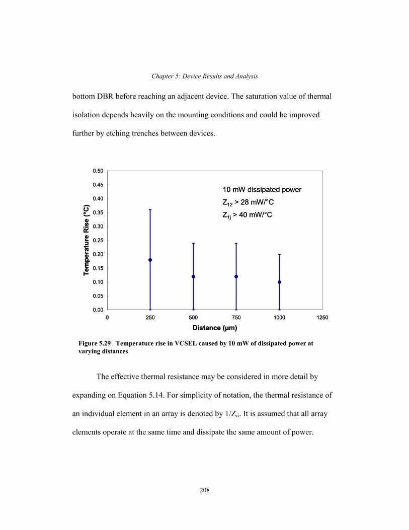
Chapter 5: Device Results and Analysis
bottom DBR before reaching an adjacent device. The saturation value of thermal
isolation depends heavily on the mounting conditions and could be improved
further by etching trenches between devices.
0.00
0.05
0.10
0.15
0.20
0.25
0.30
0.35
0.40
0.45
0.50
0 250 500 750 1000 1250
Distance (µm)
Tem
pera
ture
Ris
e (°
C)
10 mW dissipated power
Z12 > 28 mW/°C
Z1j > 40 mW/°C
0.00
0.05
0.10
0.15
0.20
0.25
0.30
0.35
0.40
0.45
0.50
0 250 500 750 1000 1250
Distance (µm)
Tem
pera
ture
Ris
e (°
C)
10 mW dissipated power
Z12 > 28 mW/°C
Z1j > 40 mW/°C
Figure 5.29 Temperature rise in VCSEL caused by 10 mW of dissipated power at varying distances
The effective thermal resistance may be considered in more detail by
expanding on Equation 5.14. For simplicity of notation, the thermal resistance of
an individual element in an array is denoted by 1/Zii. It is assumed that all array
elements operate at the same time and dissipate the same amount of power.
208

Chapter 5: Device Results and Analysis
Therefore, the effective thermal resistance of element i in an array, Ri, in an N
element array is given by:
∑=
=++=N
j ijiiii ZZZZ
R1321
1111K Equation 5.15
This form of the expression relates Ri to ∆Ti. An alternative, but equally valid
formulation would relate Ri to ∆Pi. Equation 5.14 may be extended to all array
elements by re-writing it in matrix form. Equation 5.16 expresses the temperature
rise for each element of the array in terms of the thermal isolation between
elements and the power dissipated by each element.
∆
∆∆
=
∆
∆∆
N
NNNN
N
N
N P
PP
ZZZ
ZZZ
ZZZ
T
TT
M
L
MOMM
L
L
M2
1
21
22221
11211
2
1
111
111
111
Equation 5.16
It is apparent from Equations 5.15 and 5.16 that heat flow from
neighboring devices increases the effective thermal resistance of individual lasers
in the array. In the case of an isolated 1 x N array, center elements will experience
a greater increase in temperature than the end elements for a given power
209

Chapter 5: Device Results and Analysis
dissipation by each device. This effect is plotted in Figure 5.30, using 410 K/W as
the individual VCSEL thermal resistance, as calculated in section 5.2
400
410
420
430
440
450
460
470
480
490
500
1 2 3 4
Laser Number
Effe
ctiv
e Th
erm
al R
esis
tanc
e (K
/W)
N = 1
N = 2
N = 3
N = 4
400
410
420
430
440
450
460
470
480
490
500
1 2 3 4
Laser Number
Effe
ctiv
e Th
erm
al R
esis
tanc
e (K
/W)
N = 1
N = 2
N = 3
N = 4
Figure 5.30 Effective thermal resistance for devices in 1 x N array, N = 1-4
The effective thermal resistance of a central element in a 1 x 4 array is
13% higher than that of an edge element. The increase would be even larger if not
for the large device spacing and high transverse thermal conductivity of the
GaAs/AlAs DBR. Although the effects of thermal crosstalk are not significant for
this array, they could be further mitigated by improved heat sinking. Increasing
the thermal isolation by etching a trench between devices would also reduce
crosstalk.
210
Chapter 5: Device Results and Analysis
5.5. Summary
In this chapter, the results from two generations of wafer-bonded VCSELs
were presented. The first generation of single wavelength devices was limited by
high operating voltage. However, these devices were still capable of continuous-
wave operation at ambient temperatures up to 85°C and threshold currents as low
as 0.9 mA. The second generation of devices was fabricated using the same
epitaxial material, but patterned in multiple-wavelength arrays. Due to reduced
voltage, these devices lased under continuous-wave operation up to 105°C. This is
the highest operating temperature reported for an electrically pumped 1.55 µm
VCSEL. The measured wavelength spacing was approximately 5 nm, consistent
with expectations. This is the first demonstration of an electrically pumped,
independently modulated multiple-wavelength VCSEL array at 1.55 µm.
Threshold currents were as low as 0.8 mA for a 5 µm device. The highest output
power measured was 0.65 mW. Current spreading was identified as a mechanism
limiting low threshold operation. It is expected that device performance could be
further improved with optimized aperture placement, lowered series resistance
and reduced absorption losses in p-type material. Optical and thermal crosstalk
211
Chapter 5: Device Results and Analysis
were analyzed. These effects are minimized by to the high thermal conductivity of
the GaAs-based DBRs and the large distance between devices.
References
[1] J. Piprek, Y. A. Akulova, D. I. Babic, L. A. Coldren, and J. E. Bowers,
"Minimum temperature sensitivity of 1.55 µm vertical-cavity lasers at -30
nm gain offset," Applied Physics Letters, vol. 72, pp. 1814-16, 1998.
[2] L. A. Coldren and S. Corzine, Diode Lasers and Photonic Integrated
Circuits. New York, NY: John Wiley & Sons, Inc., 1995.
[3] G. P. Agrawal and N. K. Dutta, Semiconductor Lasers. New York: Van
Nostrand Reinhold, 1993.
[4] J. Piprek, D. I. Babic, and J. E. Bowers, "Modeling and optimization of
1.54 µm double-fused VCSELs for cw operation above room
temperature," Proceedings of the SPIE, vol. 2693, pp. 149-58, 1996.
[5] E. R. Hegblom, N. M. Margalit, B. J. Thibeault, L. A. Coldren, and J. E.
Bowers, "Current spreading in apertured vertical cavity lasers,",, 1997, pp.
176-80.
[6] N. M. Margalit, "High-Temperature Long-Wavelength Vertical Cavity
Lasers," in Electrical and Computer Engineering Department. Santa
Barbara, CA: University of California, 1998.
212

Chapter 5: Device Results and Analysis
213
[7] K. A. Black, P. Abraham, A. Keating, Y. J. Chiu, E. L. Hu, and J. E.
Bowers, "Long wavelength vertical cavity lasers," Proceedings of 11th
International Conference on Indium Phosphide and Related Material, pp.
271-6, 1999.
[8] E. Hall, S. Nakagawa, G. Almuneau, J. K. Kim, and L. A. Coldren,
"Selectively etched undercut apertures in AlAsSb-based VCSELs," IEEE
Photonics Technology Letters, vol. 13, pp. 97-9, 2001.
[9] E. Hall, A. Huntington, R. L. Naone, H. Kroemer, and L. A. Coldren,
"Increased lateral oxidation rates of AlInAs on InP using short-period
superlattices," Journal of Electronic Materials, vol. 29, pp. 1100-4, 2000.
[10] S.-Y. Hu, J. Ko, O. Sjolund , and L. A. Coldren, "Optical crosstalk in
monolithically integrated multiple-wavelength vertical cavity laser arrays
for multimode WDM local-area networks," Electronics Letters, vol. 34,
pp. 676-8, 1998.
[11] T. Wipiejewski, D.B. Young, B.J. Thibeault, and L. A. Coldren, "Thermal
crosstalk in 4 x 4 vertical-cavity surface-emitting laser arrays," IEEE
Photonics Technology Letters, vol. 8, pp. 980-2, 1996.

Chapter 6: Conclusions and Future Work
6. Conclusions and Future Work 6.1. Summary of Thesis
The results presented in this dissertation represent significant achievement
in the areas of wafer bonding and vertical cavity laser fabrication. The novel
wafer bonding techniques developed were used to create high-performance
vertical cavity lasers and enable a new class of multiple wavelength VCSEL
arrays.
6.1.1. Wafer bonding
A superlattice barrier was used as a buffer layer during GaAs:InP bonding
to reduce the number of non-radiative recombination centers propagating to the
InP active region. The photoluminescence intensity from bonded active regions
with the superlattice barrier is greater than that from bonded active regions
without the superlattice barrier. This layer was incorporated into subsequent
device structures.
The same superlattice barrier was patterned prior to bonding in order to
define multiple wavelength VCSEL cavities. By selectively wet etching
superlattice periods on a specific pitch, the cavity length may be tuned across the
214

Chapter 6: Conclusions and Future Work
wafer surface. Significantly, this technique allows wavelengths to be repeated as
desired, rather than as one continuous grade. This intracavity tuning layer was
used to fabricate multiple wavelength VCSEL arrays.
6.1.2. 1.55 µm vertical cavity lasers
Continuous-wave operation was achieved at temperatures up to 105°C.
This is the highest reported lasing temperature for a 1.55 µm VCSEL. The wafer
bonding technique facilitated the integration of highly reflective, thermally
conductive GaAs/AlGaAs DBRs with InP/InGaAsP active regions. Threshold
currents as low as 0.8 mA were measured for devices with a 5 µm oxide aperture.
The peak output power at 20°C was 0.65 mW. The peak output power at 80°C
was 0.22 mW. Threshold current densities of 1.7 kA/cm2 were measured for an 11
µm device. Single-mode operation with a side-mode suppression ratio in excess
of 40 dB was observed for a 5 µm device. The improved device performance
relative to previous generations is attributed to fewer non-radiative recombination
centers in the bonded active region, lower operating voltages and reduced optical
loss in the p-DBR.
215
Chapter 6: Conclusions and Future Work
6.1.3. Multiple wavelength VCSEL arrays
Four-channel WDM VCSEL arrays were fabricated. The wavelength span
was 1509.1-1524.4 nm with channel spacing of approximately 5 nm. This is the
first demonstration of an independently addressable, multiple-wavelength VCSEL
array at 1.55 µm. Threshold currents of 1.0 mA and peak output powers of 0.5
mW were measured. Thermal and optical crosstalk were negligible, due to high
thermal conductivity in the vertical direction and 250 µm device spacing.
6.2. Future Work
High temperature performance could be further improved by introducing
new active region materials. Current spreading could be reduced by using a
lithographically defined aperture on the InP side of the bonded junction. This
aperture could also confine the optical mode. Tunnel junction injection would
reduce device resistance and absorption loss due to high electron mobility and
reduced absorption loss in n-type material. Closer channel spacing may be
achieved with thinner tuning layers or through a combination of coarse and fine
tuning mechanisms.
216

Chapter 6: Conclusions and Future Work
6.2.1. AlInGaAs active region
The traditional InGaAsP material system for long wavelength lasers is
plagued by Auger recombination and poor electron confinement. Strained active
regions have been introduced to reduce threshold current and increase differential
gain, but the problem of poor high temperature performance remains. Most laser
transmitters based on InGaAsP material require thermoelectric cooling in order to
satisfy performance standards over the desired temperature range. In order to
maintain a cost advantage over edge-emitting lasers, it is desirable for VCSELs to
operate without a thermoelectric cooler. An alternative active region material is
AlInGaAs. The conduction band offset in AlInGaAs (∆Ec = 0.72 ∆Eg) is
significantly larger than in InGaAsP (∆Ec = 0.40 ∆Eg). Using AlInGaAs as an
active region material can provide stronger electron confinement and reduced
temperature sensitivity. The suitability of this material system for high-
performance uncooled lasers has been studied extensively[1], but not yet applied
to wafer bonded VCSELs at UCSB. Even without other design improvements,
replacing the current InGaAsP active region with AlInGaAs should result in
improved high-temperature operation.
217

Chapter 6: Conclusions and Future Work
6.2.2. Current confinement
In this work, it was calculated that 30% of the injected current was lost
due to current spreading beneath the aperture. Although the oxide aperture does
provide some current confinement, the bonded junction and low doping in the p-
InP cladding cause significant spreading between the aperture and active region.
At this time, a robust aperturing technology on InP similar to the lateral oxidation
of AlGaAs on GaAs does not exist. A large device is desirable for low electrical
and thermal resistance. A well-positioned aperture is required for low threshold
current and high output power. It is proposed that a current confining aperture be
defined in the InP cladding. Ion implantation can be used to selectively disorder
the cladding and obtain lateral current confinement. Implantation prior to bonding
allows the use of shallow implant depths and angles, reducing process
complexity.
InP cladding
quantum wells
InP cladding
InP substrate
InGaAs etch stop
ion implanted InP
InP cladding
quantum wells
InP cladding
InP substrate
InGaAs etch stop
ion implanted InP
Figure 6.1 Ion implantation for InP current confinement
218

Chapter 6: Conclusions and Future Work
This technique yields a lithographically defined aperture that constricts
current on the InP side of the bonded interface. Iron is suggested as an implant
species due to the semi-insulating behavior of Fe:InP. The remaining process
steps are identical to those discussed in Chapter 4, including lateral oxidation for
mode confinement. The processed structure is shown below in Figure 6.2.
p-GaAs/Al0.9Ga0.1As DBR
p-i-n InP/InGaAsP MQW/InP
nid GaAs/AlAs DBR
semi-insulating GaAs substrate
p-contactoxide aperture
n-contact
top-emitting
Si3N4 passivationimplanted InP
p-GaAs/Al0.9Ga0.1As DBR
p-i-n InP/InGaAsP MQW/InP
nid GaAs/AlAs DBR
semi-insulating GaAs substrate
p-contactoxide aperture
n-contact
top-emitting
Si3N4 passivationimplanted InP
Figure 6.2 VCSEL device structure with ion implant in InP cladding
Ion implantation should not degrade the InP surface to an extent that
prevents bonding. However, implantation could cause excessive damage to the
quantum well region. An alternative current confining aperture could be defined
by patterning a shallow mesa structure in the InP cladding prior to bonding, as
219

Chapter 6: Conclusions and Future Work
shown in Figure 6.3. This could be accomplished with selective wet etches of
superlattice periods or an InP etch such as H3PO4:HCl.
InP cladding
quantum wells
InP cladding
InP substrate
InGaAs etch stop
shallow mesa
InP cladding
quantum wells
InP cladding
InP substrate
InGaAs etch stop
shallow mesa
Figure 6.3 Etched mesa in InP cladding
A mesa depth of 1000-2000 Å should provide sufficient depth so that the
mesa remains intact during the bonding process. This would result in a lateral
InP:air interface, mechanically supported by unetched InP, as shown in Figure
6.4. This aperture dimension is also lithographically defined. Although some
spreading into the support region is possible, current spreading should still be
reduced compared to a device with no confinement on the InP side of the bonded
junction. The mesa depth determines the aperture location and nature of the index
perturbation. The index difference (nInP =3.17, nair = 1.00 at 1550 nm) should
provide proper modal confinement in a well-designed cavity. This technique
220

Chapter 6: Conclusions and Future Work
would provide modal and current confinement without implantation or oxidation.
The active region would not be exposed to implant damage, thermal effects, or
lateral etching.
InP cladding
quantum wellsInP cladding
InP substrate
InGaAs etch stop
GaAs/AlGaAs DBR
buried aperture
InP cladding
quantum wellsInP cladding
InP substrate
InGaAs etch stop
GaAs/AlGaAs DBR
buried aperture
Figure 6.4 Buried aperture on InP side of bonded junction
6.2.3. Tunnel junction injection
High contact resistance, low hole mobility, and high absorption loss in p-
type material limit the performance of traditional p-i-n diodes in VCSEL
structures. Tunnel junctions allow the use of two n-type DBRs and only a single
thin layer of p-type material is needed in the entire structure. It should be noted
that tunnel junction injection is compatible with either of the aperturing
techniques discussed in Section 6.2.2. A tunnel junction aperture and current
221
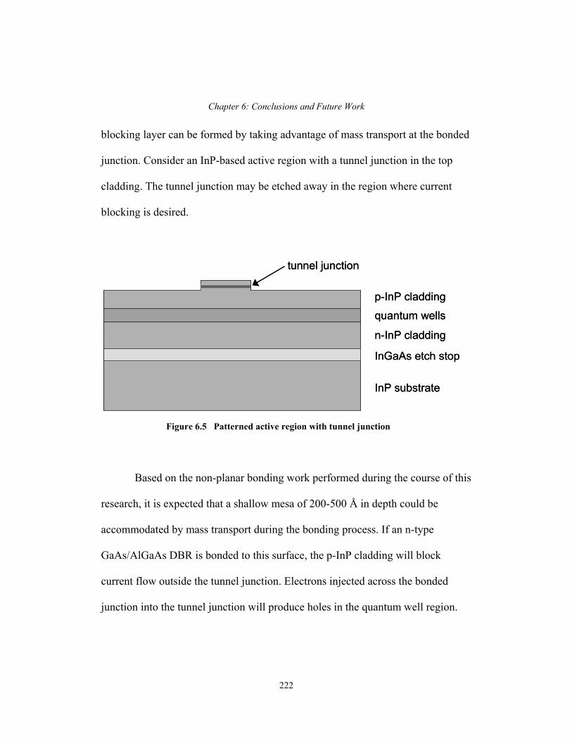
Chapter 6: Conclusions and Future Work
blocking layer can be formed by taking advantage of mass transport at the bonded
junction. Consider an InP-based active region with a tunnel junction in the top
cladding. The tunnel junction may be etched away in the region where current
blocking is desired.
p-InP cladding
quantum wells
n-InP cladding
InP substrate
InGaAs etch stop
tunnel junction
p-InP cladding
quantum wells
n-InP cladding
InP substrate
InGaAs etch stop
tunnel junction
Figure 6.5 Patterned active region with tunnel junction
Based on the non-planar bonding work performed during the course of this
research, it is expected that a shallow mesa of 200-500 Å in depth could be
accommodated by mass transport during the bonding process. If an n-type
GaAs/AlGaAs DBR is bonded to this surface, the p-InP cladding will block
current flow outside the tunnel junction. Electrons injected across the bonded
junction into the tunnel junction will produce holes in the quantum well region.
222

Chapter 6: Conclusions and Future Work
p-InP claddingquantum wells
n-InP cladding
tunnel junction
n-GaAs/AlGaAs DBR
p-InP claddingquantum wells
n-InP cladding
tunnel junction
n-GaAs/AlGaAs DBR
Figure 6.6 Tunnel junction active region with n-type DBR and current blocking layer
It may be possible to use the bonded junction itself as the n-type layer in a
tunnel junction. Capacitance-voltage measurements and simulations have
indicated a donor charge density in excess of 1014 cm-2 at the bonded interface.
This structure should also provide lateral optical confinement due to the index
difference between the tunnel junction material and AlxGa1-xAs.
There are numerous advantages to tunnel junction injection. The voltage
drop across the p-InP:p-GaAs bonded junction is replaced with ohmic transport
across n-InP:n-GaAs. This will reduce the operating voltage and series resistance
of the device. The VCSEL can now have two n-type DBRs or one n-type and one
undoped DBR. This further decreases electrical resistance and also reduces
absorption loss. Device performance will improve dramatically provided that a
suitable current confinement scheme is implemented.
223
Chapter 6: Conclusions and Future Work
6.2.4. Wavelength division multiplexing
Coarsely spaced WDM channels are desired for 10 Gigabit Ethernet
(10GbE) and other low-cost optical networks. In this work, four-channel VCSEL
arrays with a wavelength spacing of 5 nm were fabricated. For certain
applications, a higher number of more closely spaced wavelengths may be
desired. It is possible that the superlattice tuning mechanism discussed in Chapter
3 may be extended to 8 or possibly 16 channel operation by using thinner tuning
layers. However, it is unlikely that the wavelength spacing can be reduced to less
than 2 nm. Lateral oxidation techniques have been used to define multiple
wavelength cavities with smaller channel spacing but also a smaller wavelength
span. These methods including tapered oxidation[2], anodic oxidation and
regrowth[3], and variation of oxidation depth[4]. The combination of coarse
vertical and fine lateral tuning mechanisms should allow for the fabrication of
two-dimensional arrays with wide wavelength spans and narrow wavelength
spacing. Any of the lateral tuning techniques mentioned above may prove suitable
as a fine tuning mechanism. However, the lateral cavity size effect is of particular
interest since it requires neither regrowth nor long oxidations. It may also be
applied to the buried tunnel junction aperture discussed in Section 6.2.3. The
lateral size of the lasing mode defines a transverse wavevector that determines the
quasimode wavelength. If the normal component of the wave vector is kz = 2π/λ0
224
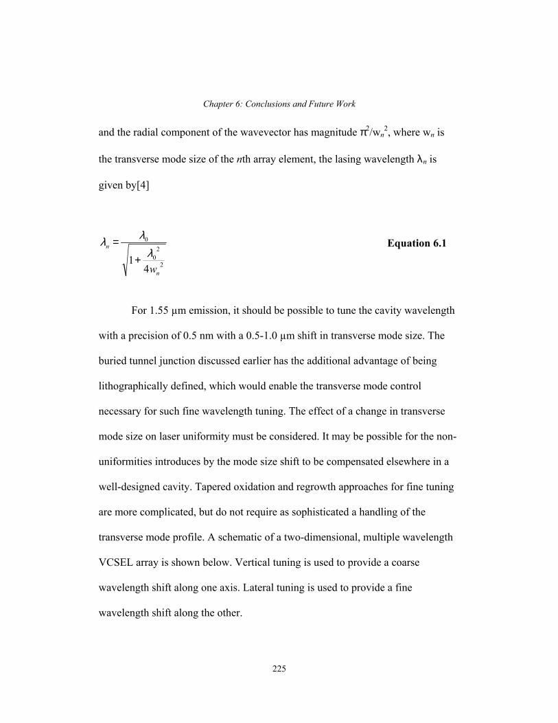
Chapter 6: Conclusions and Future Work
and the radial component of the wavevector has magnitude π2/wn2, where wn is
the transverse mode size of the nth array element, the lasing wavelength λn is
given by[4]
2
20
0
41
n
n
wλ
λλ+
= Equation 6.1
For 1.55 µm emission, it should be possible to tune the cavity wavelength
with a precision of 0.5 nm with a 0.5-1.0 µm shift in transverse mode size. The
buried tunnel junction discussed earlier has the additional advantage of being
lithographically defined, which would enable the transverse mode control
necessary for such fine wavelength tuning. The effect of a change in transverse
mode size on laser uniformity must be considered. It may be possible for the non-
uniformities introduces by the mode size shift to be compensated elsewhere in a
well-designed cavity. Tapered oxidation and regrowth approaches for fine tuning
are more complicated, but do not require as sophisticated a handling of the
transverse mode profile. A schematic of a two-dimensional, multiple wavelength
VCSEL array is shown below. Vertical tuning is used to provide a coarse
wavelength shift along one axis. Lateral tuning is used to provide a fine
wavelength shift along the other.
225

Chapter 6: Conclusions and Future Work
1534 1539 1544 1549 1554
vertical tuning (coarse)lat
eral tu
ning (fine)
1533 1538 1543 1548 1553
1532 1537 1542 1547 1552
1531 1536 1541 1546 1551
1530 1535 1540 1545 1550
1534 1539 1544 1549 15541534 1539 1544 1549 1554
vertical tuning (coarse)lat
eral tu
ning (fine)
1533 1538 1543 1548 15531533 1538 1543 1548 1553
1532 1537 1542 1547 15521532 1537 1542 1547 1552
1531 1536 1541 1546 15511531 1536 1541 1546 1551
1530 1535 1540 1545 15501530 1535 1540 1545 1550
Figure 6.7 Two-dimensional WDM VCSEL array, with vertical tuning along one axis and lateral tuning along the other. Vertical tuning is a coarse spacing mechanism to increase wavelength span. Lateral tuning is a fine spacing mechanism to reduce channel spacing. The lasing wavelength in nm is shown above each device.
226
6.3. Conclusion
Wafer bonding has been used to create a new class of vertical cavity laser
array, capable of multiple wavelength transmission in the 1.55 µm wavelength
band. These devices exhibit superior performance with continuous-wave
operation up to 105°C and threshold currents as low as 0.8 mA. Applications such
as local area networks (LANs), metropolitan area networks (MANs), and fiber to
the home (FTTH) demand low cost, high performance sources. Long wavelength
Chapter 6: Conclusions and Future Work
vertical cavity lasers will be the components that enable this next generation of
fiber optic networks.
References
[1] C. E. Zah, R. Bhat, B. N. Pathak, F. Favire, L. Wei, M. C. Wang, N. C.
Andreadakis, D. M. Hwang, M. A. Koza, L. Tein-Pei, W. Zheng, D.
Darby, D. Flanders, and J. J. Heieh, "High-performance uncooled 1.3-µm
AlxGayIn1-x-yAs/InP strained-layer quantum-well lasers for subscriber loop
applications," IEEE Journal of Quantum Electronics, vol. 30, pp. 511-23,
1994.
[2] Y.-G. Ju, D. Lofgreen, A. Fiore, H. Syn-Yem, E. Hegblom, D.
Louderback, O. Sjolund, A. Huntington, and L. A. Coldren, "Densely
packed pie shaped vertical-cavity surface-emitting laser array
incorporating a tapered one-dimensional wet oxidation," IEEE Photonics
Technology Letters, vol. 12, pp. 462-4, 2000.
[3] S. Y. Hu, J. Ko, and L. A. Coldren, "High-performance densely packed
vertical-cavity photonic integrated emitter arrays for direct-coupled WDM
applications," IEEE Photonics Technology Letters, vol. 10, pp. 766-8,
1998.
227
Chapter 6: Conclusions and Future Work
228
[4] D. L. Huffaker and D. G. Deppe, "Multiwavelength, densely-packed 2*2
vertical-cavity surface-emitting laser array fabricated using selective
oxidation," IEEE Photonics Technology Letters, vol. 8, pp. 858-60, 1996.