w. gayler - the apple ii circuit description.pdf
TRANSCRIPT


TheApple II@CircuitDescription
by Winston Gayler
HouJord tlJ. Sorns & Co., lnc.43OO WEST 62ND ST. INDIANAPOLIS, INDIANA 46268 USA
r--

Copyright C 1983 by Howard W. Sams & Co., Inc.Indianapolis, IN 46268
FIRST EDITIONFIRST PRINTING-lg83
All rights reserved. No part of this book shall bereproduced, stored in a retrieval system, ortransmitted by any means, electronic, mechanical,photocopying, recording, or otherwise, without writtenpermission from the publisher. No patent liability isassumed with respect to the use of the informationcontained herein. While every precaution has beentaken in the preparation of this book, the publisherassumes no responsibility for errors or omissions.Neither is any liability assumed for damages resultingfrom the use of the information contained herein.
International Standard Book Number: 0-672-21959-XLibrary of Congress Catalog Card Number: 82-61966
Edited by: Welborn AssociatesIllustrated by: D. B. Clemons
Printed in the United States of America.

Preface
This book is a detailed circuit description of the Apple II@ computer. Specifically, itcovers the main logic board including all revisions from the earliest through thelatest (Rev. 0 through RFI Rev. D). Also covered are the current two-piece keyboardand the older single-piece keyboard.
The intended audience includes engineers, technicians, students, and hobbyists.An attempt has been made to appeal to most skill levels and backgrounds. This isdone by dividing each chapter into two sections: Overview and Detailed CircuitAnalysis. You may choose to read one, the other, or both.
The book consists of eight chapters. Chapter 1 discusses nomenclature and sym-bols used throughout the text and figures. This chapter also contains a glossary ofterms. Chapter 2 presents a description of the Apple II computer at the block dia-gram level.
The detailed descriptions start in Chapter 3. Chapters 3 and 4 cover the systemclocks and part of the video circuitry. Chapter 5 explains the memory system andChapter 6 examines the 6502 microprocessor and the system bus. Chapters 5 and 6contain overview sections dedicated to the 4116 RAM and the 6502 microprocessor.As a result, the reader need not have prior knowledge of these devices.
The keyboard and other on-board UO are discussed in Chapter 7. The videodisplay (graphics and text) is the subject of Chapter 8. Much of the Apple's circuitryserves to generate a video signal. Due to the importance of this topic, Appendix A isincluded to provide an introduction to video techniques.
Appendix B is a gathering of all known circuit revisions of the Apple II motherboard and keyboard. While the body of the book describes the latest Apple II revi-sion, Appendix B describes differences between this latest Apple and all earlier re-visions. Appendix C contains a set of mother board and keyboard schematics. Theseschematics cover all revisions. The book concludes with a list of references.
WrNsroN D. Gevlnn
Eprron's Norn: In order to present the illustrations as large as possiblemany have been placed on the foldout pages at the back of the book. Theseillustrations are indicated with an asterisk(*) immediately following thefigure number in the text, e.g., Fig. 3-4* indicates that Fig. 3-4 is located atthe back of the book.

Achowledpents
I wish to thank fellow Apple enthusiast Dr. James Alinsky for his many suggestions
and general inspiration during the research and writing of this book. I am veryappreciative for his review, from the reader's viewpoint, of the complete manuscript.
Thanks also go to the numerous employees of Apple Computer, Inc., who as-
sisted by providing documentation and answering questions. I appreciate the assis-
tance of Apple's engineering department in coordinating much of this activity.Finally, I wish to acknowledge Stephen Wozniak who designed the Apple II,
making it all possible.

Contents
CHAPTER 1
INrnonucuoN.. .......9The Audience-Chapter Organization-Tlademarks, Patents, andCopyrights-What You Should Know-Revisions-IC and SignalNomenclature - Waveforms - Research - Glossary of Terms
CHAPTER 2
THn Appr,n II Br,ocx Drecneu .. .. 77Basic Architecture and Buses-Memory-Input/Output-Video-PowerSupply-Summary
CHAPTER 3
Cr,ocx GnNpuroR AND HonrzoNra,r, TrurNc .. .. 24Overview-Detailed Circuit Analysis-Summary
CHAPTER 4
Vrnno TrurNc .. 34Overview-Detailed Circuit Analysis-Summary
CHAPTER 5
Tnn Mprvronv SYsrnivr . .. .. . . 4IThe 41 16 -Overview-Detailed Circuit Analysis-Summary
CHAPTER 6
Tun 6502 aNn Sysrnu Bus ....... 58Overview-Detailed Circuit Analysis-Summary

8 Contents
CHAPTER 7
Ott-Bolno I/O .. ... . .. 86Overview-Detailed Circuit Analysis-Summary
CHAPTER 8
Txn Vropo Drspr,av ...104Overview-Detailed Circuit Analysis-Summary
APPENDIX A
Vropo TncxNrquEs .. . . .. ...139The Basic Video Display-Broadcast Standards-Color-Overscan-Summary
APPENDIX B
Appr,s's RnvrsroNs . ...L49Overview of Revisions-Detailed Circuit Analysis
APPENDIX C
Appr,r rr Scnpulrlcs .. .....162Revisions - Symbols - Acknowledgments
APPENDIX D
RsFEREr.rcns . ..165
Inppx ...168

CHAPTER
hfuoducfion
Have you ever wanted to know the detailed circuit operation of your Apple II@tcomputer? Perhaps you were designing a peripheral or making a modification.Maybe you were repairing an Apple. You may have just been curious about how itworks.
This book started as an exercise in understanding the Apple II hardware. Theinitial goal was to evaluate or design circuit modifications. It soon became apparentthat the information obtained would be useful to others. Thus, the plans for a bookdeveloped.
The result is a detailed circuit description and analysis of the main circuit boardand keyboard of the Apple II. In this introductory chapter, we present the organiza-tion of the book and explain some of the terms and symbols used.
THE AUDIENCE
This book is intended for engineers, technicians, students, and serious hobbyists.The engineer and hobbyist can use the descriptions and timing diagrams as a pre-paratory step to designing peripherals or modifications. The service technician canuse the timing diagrams and schematics as aids to troubleshooting. The waveformdrawings are particularly handy for troubleshooting with an oscilloscope. The stu-dent can use the Apple II for examples of practical circuit design. In many cases thereasons behind the design are presented here. All readers can use the descriptions tobetter understand how the Apple II works.
CHAPTER ORGANIZATION
Chapter 2 is a block diagram description of the Apple II mother board. There weintroduce the names such as "address multiplexer" and "video address generator"given to various functional circuit blocks. Chapter 2 contains the discussion of thepower supply, a simplified circuit description.
Chapters 3 through 8 comprise the body of the book. Each of these chapterstakes a functional part of the circuit and examines it in detail. These chapters are
fApple and Apple II are registered trademarks of Apple Computer, Inc.
10 Apple ll Circuit Description
each divided into two sections: Overview and Detailed Circuit Analysis. The Over-view presents the circuit concepts and often contains block diagrams and simplifiedtiming diagrams. If the material is new to you, you may want to read oniy theOverviews and save the Detailed Circuit Analyses until you need specific details. Onthe other hand, you may already be familiar with Apple II hardwlre. In that case,you may want to jump directly into the Detailed Circuit Analyses and skip theOverviews.
Chapter 3 presents the master oscillator, clock generator, and horizontal portionof the video address generator. Clocks are always important in a digital circuit, andthey are especially important in the Apple II due to their interpla! with the videocircuitry.
Chapter 4 completes the video address generator by presenting its vertical por-tion. The chapter also covers video sync, blanking, and color burst.
The random access memory in the Apple II is shared by the microprocessor andthe video generator. Chapter 5 covers this shared access scheme. The chapter alsocontains an introduction to the type 4116 dynamic RAM (random access memory).
Chapter 6 starts with an introduction to 6502 microprocessor hardware. Thechapter then describes all the 6502 cycle types that are .tred in the Apple. Includedare read cycles, write cycles, RAM cycles, RoM cycles, I/o cycles, keyLoard cycles,interrupts, and DMA (direct memory access).
Chapter 7 describes the Apple II on-board UO devices, such as cassette I/O, gameI/O, and speaker. This chapter also contains the circuit description for the currenttwo-piece keyboard.
The video generator is described in Chapter 8. There you will learn how text,LORES, and HIRES are generated by the hardware under software control.
Appendix A is an introduction to video signal techniques. If you are not familiarwith video signals, such as sync, blanking, and color burst, then you may want toread Appendix A. Doing so may increase your appreciation of Chapters B, 4, and 8.
Appendix B covers the topic of Apple II circuit revisions. The most recent circuitavailable (RFI mother board, Rev. D) is covered in the body of the book. Circuitvariations dating back to the earliest Apple II (Rev. 0) are then covered in AppendixB. The appendix also contains modified waveform drawings for signals that differ inearlier revisions. The circuit description for the old single-piece keyboard is con-tained in Appendix B.
Appendix C contains schematic diagrams for all revisions of the Apple II.A list of references follows the appendices-it is arranged by chapter.
TRADEMARKS, PATENTS, AND COPYRIGHTSThe names Apple, Apple II, Apple II Plus, and Applesoft are registered trademarksof Apple Computer, Inc. BASIC is a registered trademark of the trustees ofDartmouth College.
Portions of the Apple II circuitry are protected by U.S. patents 4,L80,g62;4,136,359; and 4,27 8,972.
The Apple II schematics are copyrighted by Apple computer, Inc. Theseschematics have been redrawn and printed with the permission oi Apple Computer.
WHAT YOU SHOULD KNOWAs a reader of this book, you should be familiar with TTL (transistor-transistorlogic), such as gates, flip-flops, shift registers, and multiplexers. While reading, you
r-

lntrod uction 1 1
may want to have a copy of a TTL data book, such as Reference 1.2. You need not befamiliar with the 4116 RAM or the 6502 microprocessor. Special sections in Chap-ters 5 and 6 will cover these devices. However, you should have a basic knowledge ofmicroprocessor and microcomputer architecture. And of course you should be famil-iar with the binary and hexadecimal number systems.
Concerning your Apple II background, you should be familiar with t}lre Apple IIReference Manual (Reference 1.1).
REVISIONS
There have been several circuit revisions to the Apple II since its introduction in1977. The revisions are discussed in detail in Appendix B. Here in Chapter 1 wesimply summarize the changes and establish a revision nomenclature for usethroughout the book.
There are two categories of the Apple II mother board: Non-RFI (the earlymother boards) and, RFI (recent mother boards that have been designed to reduceradio-frequency interference).
Non-RFI mother boards have the part number 820-0001-XX where XX is therevision. The first non-RFI mother board was Revision 0; we will call it simply Reu.0. It had only four HIRES colors. Revision 0 also lacked color killer and power-onreset circuits.
Reuision / came next and added two more HIRES colors (for the current total ofsix). Revision 1 also added color killer and power-on reset circuits and made othersmall changes. Revisions 2, 3, and 4 had the same circuit as Rev. 1. In this book, weinclude them with Rev. 1.
The next significant change occurred at revision ?-the memory jumper blockswere removed and the character generator IC was changed.
The next significant change occurred with the switch to the RFI mother board.This board has the part number 820-0044-XX where XX is the revision. All revi-sions of this board to date (through Rev. D) have the same functional circuit. Werefer to it simply as RFI.
The part numbers are found either along the left edge of the mother board orunder the 6502 IC. See Appendix B for more details. In summary, the mapping frommother board part numbers to our nomenclature is shown in Table 1-1.
Table 1-1 . Mapping From Mother Board Part NumbersPart No. Revision
Non-RFl
820-0001-00 Rev. 0
820-0001-01820-0001-02820-0001-03820-0001-04
Rev. 1
820-0001-07 & up Rev. 7
RFI820-0044-01820-0044-C820-0044-D
RFI
IC AND SIGNAL NOMENCLATURE
The ICs on the mother board are designated bygrid coordinates consist of the letters A through
their location onK along the left
an X-Y grid. Theedge of the board

12 Apple ll Circuit Description
and the numbers 1 through 14 along the front edge of the board (Fig. 1-1*). Withinan IC, the individual gates or sections are designated by the pin number of the gateoutput. For example, a reference in the text to "flip-flop 810-9" refers to a flip-flop inthe IC located at coordinates B10. The specific flip-flop is the one whose Q output ison pin 9.
Signals use a similar nomenclature. For example, signal "Cll-4" is the signal atpin 4 of IC C11. Some signals have already been given names on the Appleschematics-"LD194" is an example. When a signal name has a bar over it (such asFAS), it means that the signal is active low. Ail signal names are printed usinguppercase letters.
WAVEFORMS
When we say a digital signal is low, we mean it is about 0 volts. When a digitalsignal is high, we mean it is about 4 or 5 volts. The exact voltage level varies withlogic family, load, and power supply voltage. For typical 74LSXX logic, a low outputis less than 0.5 volt and a high output is greater than 2.7 volts. The same logicfamily will accept an input of less than 0.8 volt as a low, and greater than 2.0 voltsas a high. Input levels between 0.8 and 2.0 volts result in an indeterminate state.
When we say a digital IC's output signal is high impedance, we mean that theIC neither drives nor appreciably loads the signal line. The high-impedance state isthe third state of three-state logic: low, high, and high impedance. We sometimesrefer to the high-impedance state as t}ne off state. The off state of a three-state ICallows other ICs to turn on and drive a common signal line.
Digital waveforms are not drawn to vertical scale. Instead, the three possiblestates are depicted as shown at the top of Fig. 1-2. The rest of this figure shows thesymbols used for transitions between states.
RESEARCH
The research for this book consisted of two major steps: paper analysis and labora-tory verification. In the first step, the schematics were analyzed to ascertain thecircuit operation and the timing waveforms. In the second step, the waveform draw-ings were taken into the laboratory and verified using equipment, such as the fre-quency counter, oscilloscope, logic analyzer, and light pen recorder.
The two research steps were first performed on a Revision 3 non-RFI Apple II.Later, Rev. 0, Rev. 7, and RFI Apples were obtained so that waveforms unique tothese revisions could be verified. Operation and waveforms for both the single-pieceand two-piece keyboards were also confirmed. Thus, the complete set of Apple IIwaveforms presented in this book have been laboratory verified.
GLOSSARY OF TERMS
ac-Alternating current.access time-The time from accessing a memory IC (with an address or clock) until
the data becomes stable at the output.active high-A high level represents a logic 1.active low-A low level represents a logic 1.AN-Annunciator.architecture - Block diagram.ASCII-American Standard Code for Information Interchange. A common 7- or
8-bit code used by computers and peripherals.

lntroduction 13
\ HIGH HIGH
LOW IMPEDANCE
tilJ( , J
_oF
THE THREE LOGIC STATES
I N DETERM I NATE STATE (i.e.,GARBAGE)
SIGNAL GOES LOW SOMETIME BETWEENAANDB
SIGNAL GOES HIGH SOMETIME BETWEENCANDD
SIGNAL GOES FROM STABLE TO HIGH IMPEDANCE
SOMETIME BETWEEN E AND F
SIGNAL GOES FROMSOMETIME BETWEEN
HIGH IMPEDANCE TO STABLEGANDH
SIGNAL IS STABLE BETWEEN I AND J,INDETERMINATE ELSEWHERE
SIGNAL IS STABLE BETWEEN K AND L, HIGHIMPEDANCE ELSEWHERE
SIGNAL GOES FROM HIGH IMPEDANCE TOINDETERMINATE SOMETIME BETWEEN M AN.D N
SIGNAL GOES FROM HIGH IMPEDANCE TO HIGHSOMETIME BETWEEN O AND P
POSITIVE-GOING GLITCH
f
Fig. t-2. Digital waveform symbols.

14 Apple ll Circuit Description
blanking-The part of a video signal that turns off the scanning electron beamduring retrace.
bow tie-A PC board foil pattern in the shape of a bow tie. Meant to be cut to breakthe circuit.
buffer-A simple logic element used to increase the quantity of gates that a signalcan drive,
burst-(See color burst).bus-A group of signal lines that connect in common to several circuit elements.byte-Eight bits.CAS-Column Address Strobe. (Strobes column address into 4116 RAM.)clock-An often repetitive digital signal whose edges are used to advance the out-
puts of counters and flip-flops.CLR-Clear.color burst-About nine cycles of a 3.579545MH2 signal that appear in a compos-
ite video waveform just following the horizontal sync pulse; used to synchronizethe color circuitry in a tv receiver.
color killer-A circuit in a color tv set that defeats the color circuitry when a blackand white transmission is received. Its purpose is to eliminate color noise andtinting from black and white pictures. Also, a circuit in the Apple II that removesthe color burst in text mode. This is to allow the color killer in the associated tvset to function.
combinatorial Iogic-Logic consisting of just gates.complement-Opposite state in two-state logic.eomposite video-A video signal containing sync and blanking information in
addition to picture information.CRT-Cathode ray tube; usually a monitor or terminal containing a crt.CTRL-Control.DeMorgan's Theorem-states that [E : E + F, and that ATB : E B.dc-Direct current.DMA-Direct memory access; the ability of peripherals to directly access the main
memory of a system without going through the microprocessor.don't care-A signal whose logic state will not affect circuit operation.dynamic-Depending on continuous clocking or sequencing for proper operation.EPROM-Erasable programmable read-only memory.equalizing interval-The portion of a video waveform just prior to and just follow-
ing the vertical sync pulse.falling edge-Signal transition from high to low.FCC
-Federal Communications Commission.ferrite bead-A toroid or cylinder of magnetic material that is threaded with a
wire to make an inductor.fetch-To read from memory.field-One complete scan of a crt face by an electron beam.firmware-Software executing in ROM.flag-A bit or signal that stores a binary state, such as on or off, ready or not-ready,
set or cleared.frame-One complete picture displayed on the face of a crt by a scanning electron
beam; may consist of more than one field.garbage-Data that is in an in@terminate or unstable state.glitch-A usually short and usually undesirable level change in a logic signal.high-A digital signal voltage of about 4 volts.

lntrod uction 1 5
high-order-Bits representing the larger place values of a binary number.HIRES-High resolution.hold time-The time after a clock edge during which the input data to a flip-flop or
other clocked IC must remain stable.hue-Color tint (red, blue, etc.).IJz-Hertz (cycles per second).IC-Integrated circuit.INH-Inhibit.interlace-The process by which the lines of two or more fields are interleaved on
the face of a crt to create a video frame.VO-Input/output.IRQ-Interrupt request.K or k-Kilo. (x 1000 when dealing with ohms,hertz, etc., x 1024 when dealing
with memory locations, etc.)KBD-Keyboard.LORES-Low resolution.low-A digital signal voltage of about 0.
low-order-Bits representing the smaller place values of a binary number.LSB-Least significant bit (the lowest order bit).luminance-The brightness or black and white portion of a color video signal.M-Mega (x 1,000,000).mask-Tb cause to ignore.mother board-The main logic board into which peripheral boards plug.mS-Millisecond (0.001 second).MSB-Most significant bit (the highest order bit).negative true-A low level represents a logic 1.
NMI -Non-maskable
interruPt.non-interlaced-The video technique where each frame consists of one field; that
is, the field and frame are identical (see interlaced).non-maskable-Incapable of being ignored.nS-Nanosecond (10-e second).off-High-impedance state of three-state logic.on-Low-impedance state (either 0 or 1) of three-state logic.op code-Operation code; the first byte of an instruction.open collector-A logic output with two states: low (about 0 volt) and high imped-
ance.overscan-The loss of picture information caused by the electron beam scanning
beyond the edges of a crt.PC-Printed circuit.PDL-Paddle.period-Reciprocal of frequency.pixel-Picture element.positive true-A high signal represents a logic 1-.
PROM-Programmable read-only memory.RAM-Random access memory.RAS-Row address strobe (strobes row address into 4116 RAM).RDY-Ready.refresh-The process by which the data contents of a dynamic RAM are maintained
at their correct values by continuously clocking the IC.REPT-Repeat.

16 Apple ll Circuit Description
RES-Reset.retrace-The return of the scanning electron beam to the left of a crt after display-
ing a line. Also the beam's return to the top after displaying a field.RF-Radio frequency.RFI - Radio-frequency interference.rising edge-Signal transition from low to high.RoM-R€ad-only memory.R/W-Read/write.saturation-l. The intensity of color in a video signal (red is more saturated than
pink).2. The state of a linear device (such as an operational amplifier) that
is operating outside its linear range.serration-One of several narrow pulses within the vertical sync pulse. Serrations
serve to maintain horizontal synchronization during the vertical sync pulse.setup time-The time prior to a clock edge during which the data input to a flip-
flop or other clocked IC must be stable.Soft 5-A pull-up to a high TTL level.Soft Switch-A register that can be set or reset under software control. The regis-
ter then acts as a switch to control a hardware function.solder pad-A PC board foil pattern to which wire jumpers are soldered.STB-Strobe.subcarrier-A carrier that modulates a main carrier. The subcarrier itself is mod-
ulated by information to be transmitted (such as the color information in a videosignal).
SIV-Switch.sync - Synchronization.transceiver-A bidirectional buffer.TTL
-Tlansistor-transistor logic.UART - Universal Asynchronous Receiver/Tbansmitter.V-Volts.V5u-The voltage between the base and emitter of a transister; about 0.6 volt for a
forward-biased silicon transistor.wait state-An extra clock cycle inserted into the normal memory cycle of a mi-
croprocessor; used to accommodate peripherals with long access times.$-Indicates a hexadecimal number, for example: gCOFF.pS-Microsecond (10-6 second).@-Phase.*-Logical on.o-Logical .e,xo.
--Logical xor 6 : Nor A).
CHAPTER
The Apple II"Block Diagrm
In this chapter we describe the Apple II at the block diagram level. The materialwill probably not be new to most readers. It may be useful, however, to read thechapter for review. And of course if you read this material, we can then be assured ofspeaking the same language in later chapters.
We will discuss each of the blocks in the diagram and follow the signal paths forseveral major computer functions through the Apple. The Apple II block diagram isshown in Fig. 2-1.*
BASIC ARCHITECTURE AND BUSES
At first glance the Apple II's basic architecture appears to be standard for a singleboard microcomputer. There are several significantly uncommon features, however,and we will point them out as we go.
MicroprocessorAt the heart of the Apple II is the 6502 microprocessor (A in Fig. 2-1*). The 6502 isan 8-bit processor. This means that it operates on data in chunks of eight bits, or onebyte. The 6502 can directly address 64K bytes of memory. Thus, it outputs a 16-bitaddress.
Input/output (I/O) operations in the 6502 are memory mapped. This means thatVO or peripheral devices share the same 64K address space with the memory. Thereis no separate VO address space as provided in some microprocessors, such as the8080. In addition to the 8 data lines and 16 address lines, there are various clock andcontrol lines connected to the 6502. These will be described shortly.
Buses
There are three major buses in the Apple II: the 16-bit address bus, the 8-bit databus, and the control bus. These buses run throughout the computer and appear atthe eight peripheral UO connectors.
Address Bas-The 16 address lines from the 6502 are buffered by a three-statedriver (B in Fig. 2-1*) which then drives the address bus. This driver can be turned
17

18 Apple ll Circuit Description
off (switched to the high impedance state) by signal DMA from the control bus. Thefunction of Dil[A will be described shortly.
Data Bus-On write cycles, the eight data lines from the 6502 are buffered bytransceiver C which then drives the data bus. On read cycles, signal R/W (read/write) reverses the drive direction of transceiver C. This allows data from the databus to pass to the 6502.
Control Bzs -The major control bus signals are the interrupt, ready, reset,read/write, DMA-, and clock lines. There are two interrupt lines that allow periph-erals to signal the 6502 that they need its immediate attention. The first of theselines is IRQ (interrupt request). It can be selectively ignored (masked) by the 6502.The second interrupt line is iliMI (non-maskable interrupt). It cannot be ignored; the6502 always responds to NMI.
The ready line allows "slow" peripherals to momentarily stop the 6502 whilethey fetch their data and put it on the bus. The reset line allows any device con-nected to it to reset (initialize) all other devices connected to the reset line.
We have already mentioned the read/write line. Its function is to control thedirection ofdata transfers on the data bus. Data is read from naenxory or UO devicesinto the 6502. Data is written to memory or VO devices from the 6502.
Direct memory access (DMA) refers to the ability of peripheral devices to ex-change data directly with the system's memory without the need of first sendingdata through the microprocessor. During a DMA cycle, the DMA- line turns off busdriver B so that the DMA device can put its own address on the bus. Also duringDMA cycles, transceiver C does not drive the data bus. This frees that bus for datatransfers between the DMA device and the system memory.
Clocks-The system clocks are the key to controlling the timing of data andaddress transfers on the buses. The clocks are also used throughout the Apple forsuch functions as video generation. The clocks have their origin in crystal oscillatorD. Its output of about L4 M}Jz is used by clock generator T to produce the systemclocks. One of these clocks (at about 1 MHz) is supplied to the 6502. The 6502 usesthis 1 MHz clock to time its accesses to the buses. Memory and I/O devices use thesame clock to synchronize their bus accesses with the 6502.
A read or a write operation can take place in one period of the 1 MHz clock.While the 6502 is running a program, it is executing individual instructions of thatprogram. Each instruction executes in an integer number of clock cycles. On eachclock cycle, the 6502 either writes to the bus, reads from the bus, or performs aninternal operation. Each instruction consists of a mixture of these cycle types. Theshortest instruction is two clock cycles and the longest is seven.
The 6502, the buses, and such topics as interrupts and DMA will be discussed inChapter 6. The clock generator will be discussed in Chapter 3.
MEMORY
Two types of memory are provided on the Apple II mother board: ROM (read-onlymemory) and RAM (random access memory). The mother board can contain up to12K bytes of ROM and up to 48K bytes of RAM.
ROM
Up to six 2K byte ROMs (E) can be installed on the mother board. Address decoder Fdecodes the high-order address bits to provide individual chip select lines for the sixROMs. The low-order address bits connect directly to the ROMs. On ROM read cy-

The Apple ll@ Block Diagram 19
cles, the ROM's data output is placed directly on the data bus. Fig. 2-2* shows themain address and data paths through the Apple for a ROM read cycle. ROM cycleswill be discussed in detail in Chapter 6.
RAM
Up to 48K bytes of RAM (G) can be installed on the mother board. Individual RAMlocations are selected for read/write operations by addresses on the address bus. Theaddress passes through address multiplexer H on its way to the RAM. The datainput (DI) of the RAM connects directly to the data bus. This is the source of data forRAM write cycles. Fig. 2-3* shows the main address and data paths through theApple for RAM write cycles.
On RAM read cycles, the data output (DO) of the RAM is stored in latch I. Theread data then passes through data multiplexer J to the data bus. Fig. 2-4* showsthe main address and data paths through the Apple for RAM read cycles. The RAMcycles will be discussed in detail in Chapters 5 and 6.
INPUT/OUTPUT
On-Board I/O
A computer may have a large memory and a fast processor, but it is of no use unlessthe computer can communicate with humans or other machines. That communica-tion is the purpose of the computer's I/O (input/output) facilities. In the Apple II,some of the most frequently used VO devices are located on the mother board. Theseon-board I/O devices include the speaker, cassette I/O, game I/O, and keyboard (K).Although the use of on-board VO by the Apple is not unique, it is a distinguishingfeature of the Apple II.
Write to IIO -Individual
address select lines for the on-board UO are provided byaddress decoder F. The 6502 processor writes to on'board VO devices using theseaddress lines; it does not use the data bus. For example, the 6502 may address onelocation to turn an UO function on. The 6502 may then address another location toturn that same function off. It is the act of addressing specific locations that per-forms the functions. The data bus is not used.
Read from IIO -When the 6502 reads from an on-board VO device, the data busis used. Most on-board I/O devices provide just one bit, bit 7. This single data bit(D7) connects directly to the data bus as shown in Fig. 2-1*. The keyboard is anexception since it provides seven data bits. Fig. 2-5* shows the address and datapaths for a keyboard read cycle. When the 6502 reads the keyboard, the keyboarddata passes through multiplexer J. Keyboard cycles are described in Chapter 6.
Soft Switches -The soft switches are output locations that let the Appleconfigure its own hardware. The soft switches are set under software control toconfigure the video circuitry for various display modes. Their names of TEXTMODE, MIX MODE, PAGE 2, and, HIRES MODE suggest this application.
On-board I/O is discussed in detail in Chapter 7. The soft switches are also dis-cussed in Chapters 5 and 8.
Peripheral I/O
There is a need for flexibility and expansion beyond the on-board VO. Tb meet thisneed, the Apple II mother board is provided with eight 50-pin peripheral connectors(L in Fig. 2-I*). The address, data, and control buses appear at each connector. Each

20 Apple ll Circuit Description
connector is also provided with individual select lines from address decoder F. Theselect lines reduce the amount of address decoding circuitry needed on each periph-eral card. This feature of the Apple II will be discussed in detail in Chapter 6.
VIDEOThe video output of the Apple contains text and graphics information for display ona monitor, or tv set. Video signals require high-frequency components that are toofast to be generated directly by the 6502 microprocessor. (If you are not familiarwith video signals, you may wish to review Appendix A at this time.) As a result ofthe high frequencies, dedicated hardware is provided to generate the Apple's videooutput. Of course, software-control gives the 6502 command over this hardware togenerate specific text and graphics patterns.
The patterns that are to be displayed on the screen are generated by the 6502and stored as data in the RAM in the Apple. The video circuitry then reads the datafrom the RAM, converts it to a video format, and sends it to the video output fordisplay on a monitor. The accesses to RAM by the 6502 and the video circuitry aretime-shared as described here. During the first half of a 6502 cycle, the video cir-cuitry reads ftom RAM. During the second half of the cycle, the 6502 reads fromRAM or writes to RAM.
In the sections that follow, we will examine the blocks in Fig. 2-L" that comprisethe video circuitry.
Video Address GeneratorUsing the system clock as a reference, video address generator M creates a 15-bituideo address. The video address consists of six horizontal bits and nine vertical bits.The address is continuously running through an incrementing sequence that repeatsabout 60 times a second. During each pass through the sequence, the vertical ad-dress has 262 different values. For each value of vertical address, the horizontaladdress increments through 65 counts.
Tbgether, the horizontal and vertical addresses can select a location anywhereon the screen. Each screen location has a height of one scan line, and a width ofabout one microsecond. The video address also includes locations that do not appearon the screen since they occur during horizontal or vertical blanking.
Each location on the screen corresponds to a unique video address. As we willsee shortly, the scanning electron beam in the crt is synchronized to the video ad-dress. One function of the video address is to "tell" other hardware sections thecurrent screen location of the beam. The other hardware sections then fetch theappropriate character or graphics symbol for display at that location.
Fig. 2-1* shows a feedback path from the video address generator to the clockgenerator. This feedback signal delays the system clock by about 140 nS every hori-zontal scan line. The purpose of this unique arrangement is to simplify the genera-tion of color graphics-it will be described in Chapter 3.
Memory MapperThe video address is not a bit-for-bit equal of the memory address used to store thecorresponding screen data. As a result, the video address must be converted to amemory address in order to fetch the correct screen data from memory. Memorymapper N performs this function. Screen locations go into the mapper, and the cor-responding memory location comes out.

The Apple ll@ Block Diagram 21
The memory mapper will map to different memory address blocks under controlof the soft switches. In HIRES mode, for example, the video address maps to a differ-ent memory range than it would in text mode.
Fig. 2-6* shows the path through the Apple for a video cycle. The video addressgoes into the memory mapper and the memory address comes out. During videocycles, address multiplexer H connects the output of the mapper to the address inputof the RAM. Data out of the RAM is then stored in latch I. The latched data thenappears as an input to video generator P.
Video GeneratorThe video generator configures the latched data into video data that it sends tomixer Q. In the mixer, the video data is combined with the sync and color burstsignals to become the composite video output.
The conversion process in the video generator is controlled by the soft switches.In LORES mode, for example, the video generator acts on the data in a mannerdifferent from the way it would act on the same data in text mode.
Sync GeneratorSync generator R uses the video address to generate the sync, color burst, and blank-ing signals. SYNC and COLOR BURST are mixed with the video in mixer Q. Thesync component of the composite video output allows the scanning electron beam inthe display crt to synchronize with the video address. The color burst componentallows the color circuitry in the display device to synchronize with the internal colorreference clock of the Apple. BLANKING connects to the video generator where itforces the video signal to go black during the horizontal and vertical blanking inter-vals.
POWER SUPPLY
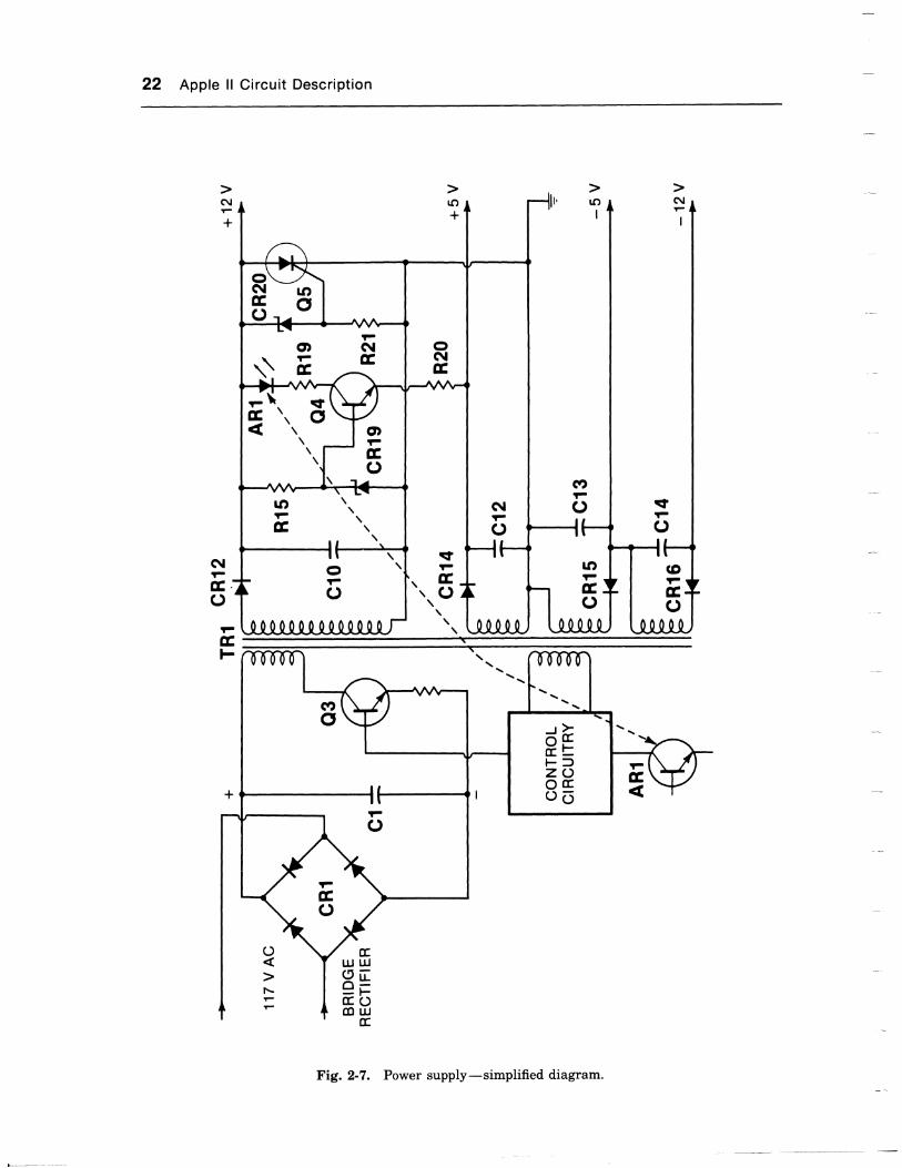
The Apple II is equipped with a switching power supply that provides *5 V, +12 V,-5 V and -12 V to the mother board, keyboard, and peripheral I/O connectors.Switching power supplies are noted for their higher efficiency and lower bulk thanmore conventional designs. The power supply design of the Apple eliminates theneed for a heavy line transformer. The ac line input is rectified, then converted to ahigh-frequency ac. This high-frequency ac is then coupled to the secondary of thesupply via a small transformer.
Basic OperationFig. 2-7 is a simplified diagram of the power supply. Bridge rectifier CRl rectifiesthe ac line input to provide a dc potential that is filtered by Cl. This dc potentialcauses a current to flow through a primary winding of transformer TRl when QB ison. Tbansistor Q3 switches on and off at a high frequency. On each cycle, energy isstored in TRl while Q3 is on. When Q3 turns off, this energ:y is coupled to thesecondary windings and causes current to flow in the output load.
Circuitry is provided to control the conduction of Q3 via its base. This controlcircuitry derives its operating potential from a second primary winding of TRl.
At the secondary, rectifier diodes and filter capacitors are used to obtain the fourdc output potentials.
Regulation-Thansistor Q4 is wired as a comparator that senses the voltage onthe +5 V output. Resistor RL5 and zener diode CR19 derive a reference voltage from
22 Apple ll Circuit Description
o)
$E\ \\\
l()\F\Et..
CDFO <r
Fo
(0Ft,o
l(lFEo
stl-eE;()
FG,F
CT[rJ Lu
8E-FEOd]ru
E.
C)
lt-r
Fig. 2-7. Power supply-simplified diagram.

The Apple ll@ Block Diagram 23
the +12 V output. This reference is applied to the base of Q4. The emitter of Q4 isconnected through R20 to the +5 V output. When Q4 conducts, current flowsthrough the LED (light emitting diode) that is part of optical coupler ARl. Theamount of light emitted is a function of the voltage on the +5 V output. If the +5 Voutput decreases, for example, Q4 conducts more heavily and the LED emits morelight. This light is coupled to the phototransistor portion of ARl. Increasing lightcauses the phototransistor to conduct more heavily. Via the control circuitry, thisfeedback causes QB to deliver more energy to TR1. This will in turn increase thevoltage on the +5 V output. The other three voltages will track the regulation of the+5 V output.
Oueruoltage-In the event of a fault that causes an overvoltage, the increasedpotential on the +L2 V output will cause zener diode CR20 to conduct. This makesthe gate of silicon controlled rectifier Q5 go positive-Q5 conducts, shorting the +12V output to ground. This action will shut down the whole supply.
The complete power supply schematic is shown in Fig. C-23*. CAUTION: Thisschematic is reprinted directly from the Apple II Reference ManuaL lt has not beenverified for accuracy with respect to any product shipped by Apple Computer. Youare also cautioned against attempting to repair or modify your power supply. Muchof the circuitry is not isolated from the ac line input and thus contains hazardousvoltages. If you wish to read additional material on the power supply, obtain a copyof U.S. Patent No. 4,130,862.
SUMMARY
In this chapter we have presented a brief overview of the Apple II computer. At theheart of the Apple II is a basic single-board microcomputer consisting of micro-processor, buses, bus drivers, bus transceivers, ROM, and RAM. This basic architec-ture is enhanced by the inclusion of on-board I/O for many of the frequently used I/Ofunctions. Expandability is provided by eight peripheral I/O connectors. The use ofthese connectors is simplified by an address decoding scheme that provides individ-ual select lines for each connector.
A large part of the Apple II hardware consists of the built-in video text andgraphics capability. Since the video screen memory resides in the address space ofthe microprocessor, the microprocessor can quickly output data to the screen with asimple memory write operation. Access to the screen memory is time-shared by themicroprocessor and the video circuitry. This is an efficient arrangement that doesnot slow the processor.
In the chapters that follow, we will examine in detail the elements that make upthe Apple II block diagram. We start in the next chapter with the clock generator.

CHAPTER
Clock Generator andHofuntd g
We begin our discussion of the Apple II with signals that are essential for the opera-tion of the computer, the clocks. While it might not be very exciting, a knowledge ofthe clocks will provide a basis for the explanation of many of the functions of theApple. In this chapter we will derive the clocks and horizontal timing and makesome interesting discoveries about the processing speed of the 6502.
Schematic reference: Figs. C-2* and C-3*.
ovERvrEwClocksThe Apple II circuit design is based on clocked logic. There are thus many flip-flops,counters, and shift registers. These circuit elements all perform their tasks uponreceiving a signal transition (or edge) at their clock inputs. For example, a 74LS161counter will count and update its output pins upon receiving a rising edge at itsclock input. The counter then sits idle until the next clock edge is received. Clearlythe faster the clock, the higher the throughput. If the clock is too fast, however, thecircuitry may not have time to respond between clock edges. The 74LS161, forexample, may not respond to clock frequencies higher than 25 MHz.
Other devices in the Apple also use clocks. The 6502 microprocessor advancesthrough a program one step at a time as it receives its clock input. The 6502 used inthe Apple II is limited to a clock frequency of 1 MHz.
The type 4116 dynamic RAMs are also clocked devices. They load their addressinputs upon receiving a clock edge. The RAMs in the Apple II are accessed at a 2MHz rate.
The composite video output of the Apple contains an accurate 3.579545 MHzcolor reference signal. This signal is derived in the clock generator.
As you can see, there is a requirement in the Apple II for several clocks ofdifferent frequencies. By deriving the various clocks from a common high frequencymaster oscillator, all sections of the Apple are made to operate synchronously witheach other. Synchronous operation is a highly desirable trait in a digital system.
The master oscillator is selected to be an integer multiple of the individual clock
24
Clock Generator and Horizontal Timing 25
frequency that is the most critical. In the Apple, the color reference is the mostcritical frequency, and the multiplication factor is 4. Thus, the master oscillatorfrequency is 4 x 3.579545 MHz : 14.31818 MHz. The Apple makes use of countersand shift registers to divide the master oscillator frequency into the various lowerfrequencies required.
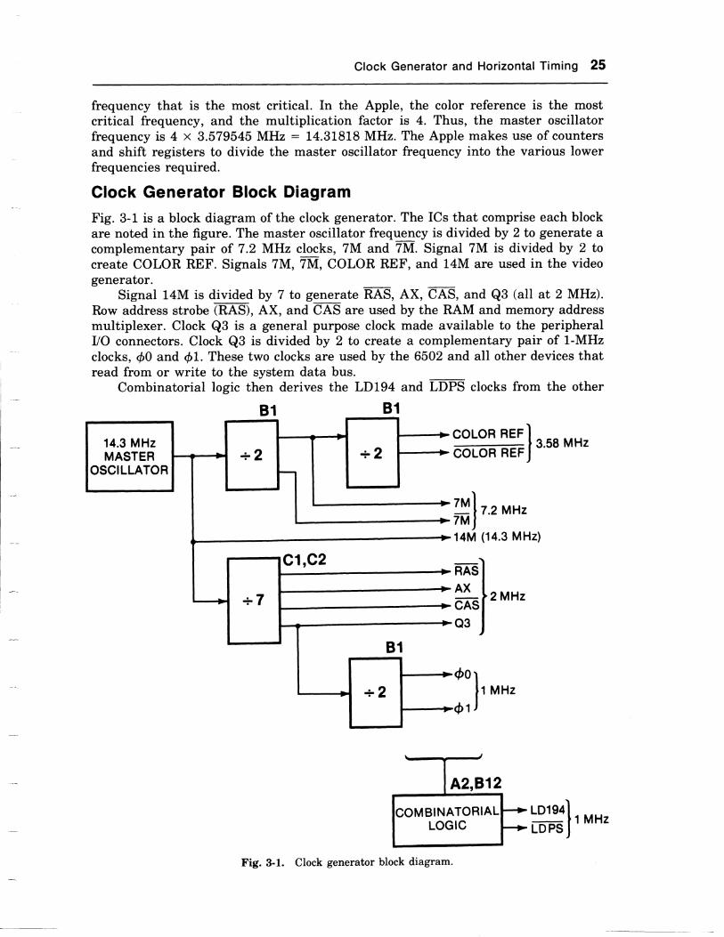
Clock Generator Block Diagram
Fig. 3-1 is a block diagram of the clock generator. The ICs that comprise each blockare noted in the figure. The master oscillator freqrlgncy is divided by 2 to generate acomplementary pair of 7.2 MHz clocks, 7M and 7M. Signal 7M is divided by 2 tocreate COLOR REF. Signals 7M, 7M, COI,OR REF, and 14M are used in the videogenerator.
Signal 14M is di"id"d by 7 to generate RAS, AX, CAS, and QB (all at 2 MHz).Row address strobe (RAS), AX, and CAS are used by the RAM and memory addressmultiplexer. Clock QB is a general purpose clock made available to the peripheralVO connectors. Clock Q3 is divided by 2 to create a complementary pair of l-MHzclocks, @0 and {1. These two clocks are used by the 6502 and all other devices thatread from or write to the system data bus.
Combinatorial logic then derives the LD194 and LIIPS clocks from the other
81 81
3.58 MHz
MHz
rylr.rMHz7MJ14M (14.3 MHz)
-\RAS I
*[,",.,Q3 l
l,]'
14.3 MHzMASTER
OSCILLATOR
cl ,c2
A2,r312
COMBINATORIALLOGIC
Fig. 3-1. Clock generator block diagram.
26 Apple ll Circuit Description
clocks previously described. LD194 is used in the video generator and LDPS is usedin the video address generator.
Video Address GeneratorThe video address generator (Fig. C-3*) consists of a stringof counters. These count-ers increment every microsecond to generate a new video address. The video addressrepresents the instantaneous screen location of the scanning electron beam in themonitor connected to the Apple. The video address is used to fetch the video datathat is to be displayed at each screen location. The video address is comprised ofhorizontal and vertical parts. The six bits of the horizontal part (H0 through H5)select one of 40 visible screen locations along a scan line. Later chapters will coverthe use of the video address. In this chapter, however, we must examine the horizon-tal video address in detail. This is due to a feedback path from the video addressgenerator to the clock generator. This feedback path plays a key role in the opera-tion of the clock generator.
DETAI LED CIRCUIT ANALYSIS
Clock Generator
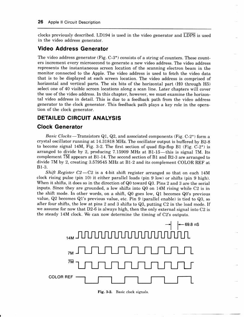
Basic Clocks-lYansistors Q1, Q2, and associated components (Fig. C-2*) form acrystal oscillator running at 14.31818 MHz. The oscillator output is buffered by B2-8to become signal 14M, Fig. 3-2. The first section of quad flip-flop 81 (Fig. C-2*) isarranged to divide by 2, producing 7.t5909 MHz at B1-15-this is signal 7M. Itscomplement 7M appears at BI-L4. The second section of 81 and B2-3 are arranged todivide 7M by 2, creating 3.579545 MHz at B1-2 and its complement COLOR REF atB1-3.
Shift Register C2 -C2 is a 4-bit shift register arranged so that on each 14Mclock rising pulse (pin 10) it either parallel loads (pin 9 low) or shifts (pin t high).When it shifts, it does so in the direction of Q0 toward Q3. Pins 2 and.3 are the serialinputs. Since they are grounded, a low shifts into Q0 on 14M rising while C2 is inthe shift mode. In other words, on a shift, Q0 goes low, Q1 becomes QO's previousvalue, Q2 becomes Ql's previous value, etc. Pin 9 (parallel enable) is tied to Q3, soafter four shifts, the low at pins 2 and 3 shifts to Q3, putting C2 in'the load mode. Ifwe assume for now that D2-6 is always high, then the only external signal into C2 isthe steady 14M clock. We can now determine the timing of C2's outputs.
-J f 6e8 ns
14M
7M
ro
COLOR REF
Fig. 3-2. Basic clock signals.

Clock Generator and Horizontal Timing 27
More Clocfts-Referring to Fig. 3-3, let's start at the point where the low hasjust shifted into Q3 (point A). Shift register C2 is a synchronous load device, so afterthe next clock pulse the outputs will take on the values of the parallel inputs thatexisted before the clock pulse. Signal Q0 m will remain low since PO (AX) waslow. Signal Ql (AX) will go high since Pl is assumed to be high for now. Signal Q2(CS will remain low since P2 (AX) was low. And finally, Q3 will stay low since P3
GIS was low.We are now at point B and still in the load mode. This time P0 and P2 (AX) are
high, so on the next clock pulse, a0 (RT) and Q2 (CAS will both go high. On thethird load, QB goes high since PB (RAS) was high. We now stay in shift mode for fourclock cycles before the low shifts into QB to put us back into the load mode. You cansee the low's shifting along at points E, F, G, and H. The cycle begins again at pointH which is the equivalent of point A. Since this cycle takes seven clock periods, RAS,AX, em, and QB all have a frequency of 14.31818 MHz + '7 : 2.045454 MHz.
Microprocessor Clock-The circuit next divides by 2 to get the microprocessor'sclock frequency of about 1 MHz. The third flip-flop in 81 (Fig. C-2) performs thisfunction, aided by data selector C1-9. The 1 MHz signal that we are looking for willbe at 81-10. The fourth 81 flip-flop delays 81-10 by one 14M clock pulse to generate
{0 at B1-7. Let's start with pins 10 and 7 of 81 low; this is in line with point A ofFig. 3-3. With both AX and {0 low, select inputs S0 and 31 of Cl are low, and inputpin 10 is gated to output pin g. Thus, the low at 81-10 appears at Bl-t2. Both B1-10and B1-7 remain low after the next clock edge, and we move to point B in Fig. 3-3.
At point B, AX is high, causing C1-9 (FiS. C-2*) to select input pin 11. Pin C1-11connects to C2-LL and is high at this time. On the next clock pulse, 81-10 goes highand we move to point C (Fig. 3-3). The select inputs of Cl do not change, so on thenext clock pulse, 81-10 stays high and 8L-7 goes high to follow 81-10. We are now atpoint D. With B1-7 high, C1-9 selects input pin 13 which is high. Nothing changeson the following clocks until AX falls. Now C1-9 selects input pin 12 which is high.Still there is no change until Q3 falls at point H causing C1-9 to select input pin 10.
Still no change until AX rises at point I. This selects C1-9 input pin 13 which is nowlow. On the next clock pulse, 81-10 falls and we move to point J. The select inputs ofCl do not change but B1-7 follows 81-10 to go low at point K. With B1-7 low, C1-9selects input pin 11 which is low, so there is no change at point M. Signal AX is lowat point N causing C1-9 to select input pin 10. Pin 10 is low, so there is no change atpoint O. The cycle begins again at point P which is the equivalent of point A.
Since this cycle takes 14 clock periods, signal @0 has a frequency of 14.31818 +L4 or about 1 MHz. Phase 1 at 81-6 is the complement of @0. Phase d0 and @1 arethe clocks for the 6502 microprocessor.
ID-PS Clock-The signal mPS is obtained by the combinatorial logic of gates813-10 and A2-3 (Fig. C-2*). When AX is Iow and CAS is Iow and @0 is high, thenf,DPS is low; see Fig. 3-3. Even though the waveforms in Figs. 3-2 and 3-3 are allderived from 14M, we have not combined them on one drawing yet since we do notknow their relative phase. This will come later after we develop some of the videotiming.
Horizontal TimingIn Fig. C-3* (Video Address Generator), D11, D12, D13, and D14 are a string of 4-bitbinary counters chained together to provide the video address. The counters clock onthel,D-PS signal when it is rising. On each clock pulse, each counter will either

28 Apple ll Circuit Description
I t*6e8ns14M
C2 MODE
c2-Qo 1HE)
c2-Q1 (AX)
c2-Q21cEyc2-Q3 (as)
81-10
B1-7 (00)81-6 (01)
LDPS
ltt*S = SHIFT
L = LOAD
Fig. 3-3. Simplified system timing.
count (advance in binary sequence) or parallel load from its P inputs. The 74LS161counts when pin g is high and loads when pin 9 is low.
The first seven counter bits (H0, H!,Il2, H3, H4, H5, and trPEl have the poten-tial for 128 counts. Only 65 counts are used here. Let's start with all seven bits low,point A in Fig. 3-4*. Since EPE is low, D13 and D14 are in the load mode. On thenext clock pulse (LDPS rising), the six low order bits load in zeros (so remain low),and HPE loads in a 1 (so goes high). We are now at point B and in the count mode.Counter D14 now counts up to 15 at which time its carry output (pin 15) goes high(point C in Fig. 3-4*). This enables D13 so that on the next clock D13 counts (H4goes high). Counter D14 simply counts from 15 back to 0 and we are at point D. Theenable input of D13 is removed (D14-15 low), so D13 does not count again until D14reaches a count of 15 at E. Counter D13 counts at point F and again at points G andH. At point H, HPE is low again and the cycle restarts.
The decimal values of the bits H0 through H5 are shown in Fig. 3-4*. Note thatthere are two counts in the cycle with the value 0, and that there are 65 counts totalper cycle. Counters D13 and D14 thus divide LD-PS by 65. Each cycle (65 counts)through the waveforms of Fig. 3-4* corresponds to one horizontal line of the Applevideo output. Each of the 65 counts corresponds to the width on the screen of onecharacter in text mode (or one pixel in LORES mode). We know that the Apple
:I€ S L L LSSS S L LLS S S S L L Ls sS
Clock Generator and Horizontal Timing 29
displays only 40 characters per line. It so happens that the other 25 counts occur
during horizontal blanking. There will be much more on this in later chapters. Firstlet's examine how HPE feeds back to the clock generator to affect shift register C2.
Note: The remainder of the waveforms in Fig. 3-4* will be discussed in Chapter 4.
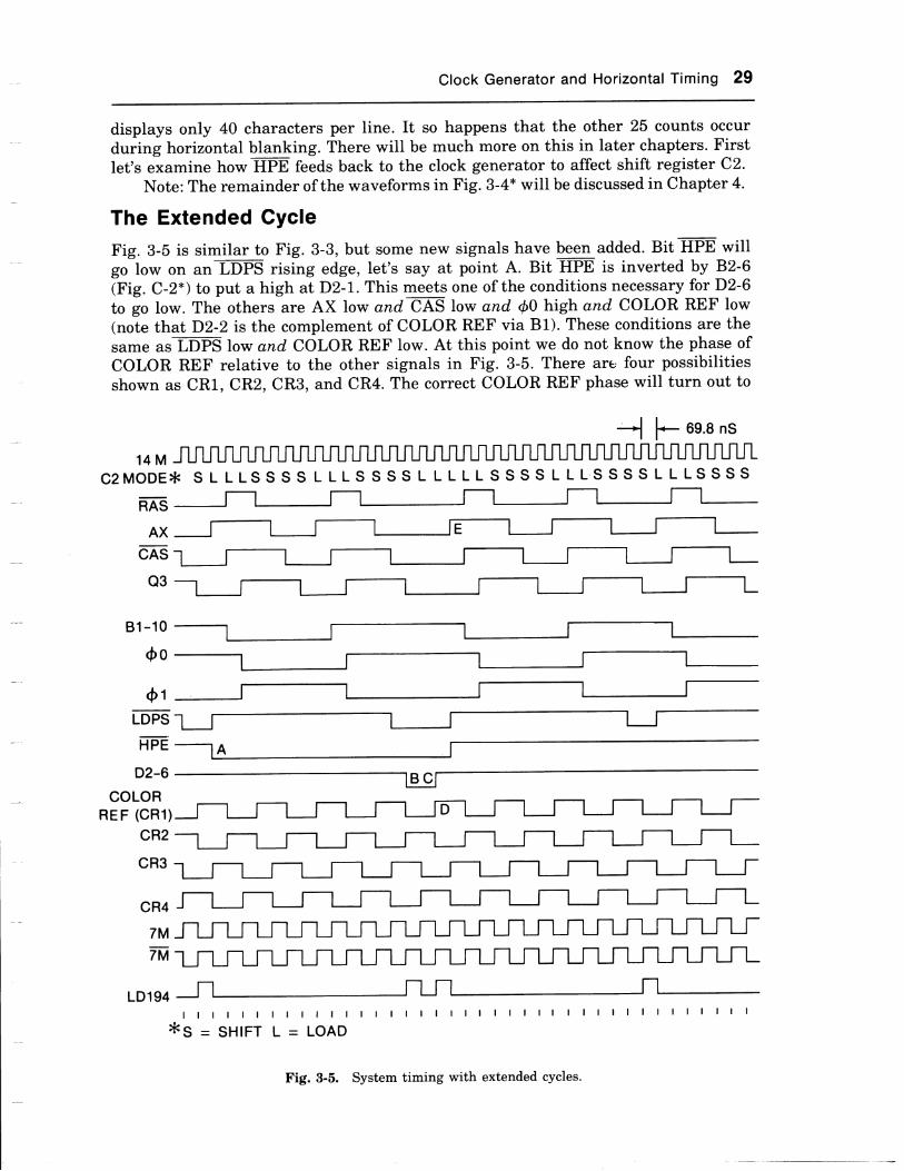
The Extended Gycle
Fig. 3-5 is similar to Fig. 3-3, but some new signals have been added. Bit HPE willgo low on an LDPS rising edge, let's say at point A. Bit EPE- is inverted by B.2-6(Fig. C-2*) to put a high atD2-t. This meets one of the conditions necessary for D2-6
to go low. The others are AX low ondG low and @0 high and COLOR REF low(note that D2-2 is the complement of COLOR REF via B1). These conditions are thesame as LDPS \ow and COLOR REF low. At this point we do not know the phase ofCOLOR REF relative to the other signals in Fig. 3-5. There are four possibilitiesshown as CRl, CR2, CR3, and CR4. The correct COLOR REF phase will turn out to
*l F 6e.8 ns
14Mc2 MODE {< SLLLSSS LSSL
FTs
AX
cns
Q3
81-10
0o
rftLDPS
FFE
D2-6
COLORRE F (CR1)
cR2
cR3
cR4
7M
Tlrl
LD194lttlllllllll ll I ll lllllll ll I lll llll lll ll
*s=sHtFTL=LoAD
Fig. 3-5. System timing with extended cycles.

30 Apple Il Circuit Description
be CRl. Assume for now that our Apple powers up with COLOR REF shown as CR1;we will worry about the other three cases later.
Everything proceeds as previously described until point B when LDPS andCOLOR REF are both low. Pulse D2-6 goes low, so that on the next clock cycle a lowloads into AX instead of the usual high. We are now at point C and another lowIoads into AX. At point D, COLOR REF and D2-6 go high so that on the next clockpulse AX goes high (point E). The timing continues from this point as previouslydescribed in Fig. 3-3. The result of the low at HPE is to extend MS, AX, CAS, Q3,00, 01, and LDPS for two 14M clock cycles. The normal cycle is 14 + 14.31818 MHz: 978 nS (nanoseconds). The extended cycle is 16 + 14.31818 MHz : 1117 nS. Inother words, most 6502 cycles are 978 nS long, but every 65th cycle is 1117 nS long.The average processor speed is then
65L4.31818 MHz x rc4 x 14) + 16 - L.020484 MHz.
The horizontal video frequency is 1.020484 MHz + 6b : 15.200 kHz.Why the extended cycle every horizontal line? For the Apple to work with color
tv sets, the frequency of COLOR REF must be very close to 3.579545 MHz. This hasbeen achieved. Also, the horizontal frequency must be near (but need not be exactly)15'734 kHz. Without the extended cycles, the circuit would divide 14M by (14 x 6b).Since
14.31818 MHz14 x 65
it would appear that the second requirement is easily met. It is, but there is a com-plication. Note that COLOR REF divided by this horizontal frequency is 3.579545MHz + 15.734 kHz : 227.5. Every horizontal line would contain 227 and one-halfcycles of COLOR REF. COLOR REF would thus change phase by 180 degrees oneach line relative to what it was on the previous line. There are two ways to dealwith this:
1. Change the phase of the color data every line to compensate for the change inCOLOR REF.
2. Choose another horizontal frequency such that one horizontal line would con-tain an integer number of cycles of COLOR REF.
The Apple II design uses Number 2. The 227.5 ratio is increased to 228 by ex-tending each line by one-half period of COLOR REF. Note that one-half period ofCOLOR REF equals two full periods of 14M. The horizontal frequency now becomes3.579545 MHz + 228 : 15.700 kHz, a number derived previously. This horizontalfrequency is close enough to 15.734 kHz for most tv sets. The extended cycle designof the Apple II is a major claim of U.S. Patent No. 4,136,8bg.
Synchronization of Glocks
What about the cases where COLOR REF and the other clocks do not start in correctphase at power up (Fig. 3-5)? We will take each of the alternative phases (CR2, CR3,and CR4) and examine what they do while EPE- is low.
cR2-we start with CR2 in Fig. 3-6. At point A, D2-6 goes low. Register C2shifts on the next clock pulse, so this low has no effect. D2-6 goes high again at pointB. Since the cycle was not extended, CR2 will have an extra one-half period left over
I-

Glock Generator and Horizontal Timing 31
cr-ouJA-I(L
zt-
stcrouJaI-(LILoFJO l- ,^\5AIO
AJilil
AJ+9
lH I qbor!C)
taIrL
l3
X
=
==
=c
=
E==
=
=
===
:
Fig. 3-6. Clock synchronization-CR2.

32 Apple ll Circuit Descripiion
at the end of the line. The next time HPE is low (point C), COLOR REF will haveshifted 180 degrees relative to EPE. (Examine point C relative to point D, and pointE relative to point F to see the 180 degree shift.) COLOR REF now has phase CR1.When D2-6 goes low at point G, the cycle is extended as previously described. Thecorrect COLOR REF phase has now been established.
CR3-Next we examine CR3 in Fig. 3-7*. Phase CR3 is high (point A) whenLDPS is low (point B). Thus, D2-6 does not go low, and there is no extended cycle.However, as in the case of CR2 previously, on the next HPE low, CR3 will haveshifted 180 degrees. Phase CRB has now become CR4. (Tb see the 180 degree shift,examine point C relative to point D, and point E relative to point F.)
CR4-We continue now with CR4. SignaI D2-6 is low at point G and C2 shiftson the next clock pulse. Signal D2-6 is low again at point H and on the next clock
Table 3-1 Summ ary of Signals in Chapter 3
Signal Description Remarks Frequency Period
14M 14 MHz Master Oscillator 14.31 818 MHz 69.8 nS
7M 7 MHz 7.1 5909 MHz 140 nS
7M 7 MHz Complement of 7M 7.15909 MHz 140 nS
COLORREF
ColorReference
Used for Color Burst 3.579545 MHz 279 nS
EA-S RowAdd ressStrobe
Used by RAM andAddress Multiplexer
2.040968 MHz(Average)
489or628
NS
NS
AX Add ressMultiplex
m ColumnAdd ressStrobe
Q3 General Purpose Clock
00 Phase O 6502 Clock 1.020484 MHz(Average)
978 nSor
1117 nS
o1 Phase 1 Complement of ,00
I
i rDPs Load Parallelto Serial
Clock for Video AddressGenerator and Load forText
LD194 Load(741S) 1s4
Load for Graphics Data
HO Horizontal 0 Horizontal Video Address
H1 Horizontal 1
H2 Horizontal 2
H3 Horizontal 3
H4 Horizontal 4
H5 Horizontal 5 15.700 kHz 63.7 g.S
HFtr HorizontalParallelEnable
Load for HorizontalVideo Address Counters

Clock Generator and Horizontal Timing 33
pulse a low loads into AX. At point I, COLOR REF is high, so on the next clockpulse, AX loads a high (point J) and the timing continues as usual. The cycle hasbeen extended by only one 14M period. The result of this extension is to convertCOLOR REF from phase CR4 to phase CRl. (By examining point K relative to pointM, and point N relative to point 0, you can see that the phase established im-mediately following the extension is indeed phase CR1.) Once phase CRl has beenestablished, there will be an extended cycle (point P) everytime HPE is low.
No matter which of the four phases COLOR REF takes at power up, it willquickly assume CRl. Phases CR2, CR3, and CR4 exist only momentarily at powerup. It may avoid confusion to note that the absolute phase of COLOR REF does notreally change after power up. The absolute phases of the other clocks do change as aresult of extended cycles. References previously to a change in COLOR REF's phasemean a change relatiue to the other clocks.
SUMMARY
Now that the correct phase for COLOR REF has been established, 7M and ruf can betransferred from Fig. 3-2 to FiS.. 3-5. We can also add LD194 which is 7M high and
@0 high and AX Iow and CAS low-LD194 is used later in the video generator.Thble 3-1 is a summary of the signals presented so far.
In the next chapter we will complete the description of the video addressgenerator. We will then examine the portion of the video generator that creates thevideo sync, video blanking, and color burst signals.

CHAPTER
Video g
This chapter continues the analysis of the video address generator that was startedin Chapter 3. First we will finish the investigation of the D11, D12, D13, and D14counter chain in order to develop the vertical timing. Then we will combine thehorizontal and vertical timing to create the video sync, the video blanking, and thecolor burst signals.
Schematic reference: Figs. C-3*, C-16*, and C-20*.
OVERVIEW
Vertical TimingJust as we needed a horizontal video address counter to define the horizontal posi-tion of the video data at any instant in time, we need a vertical address counter todefine the vertical position of the video data. The horizontal and vertical addresscounters are not independent. The crt beam must trace a complete horizontal linebefore the vertical counter can advance to the next line (see Appendix A for anexplanation of video techniques). The vertical counter advances once each time thehorizontal counter runs through a complete count of 65. Each count of the verticalcounter corresponds to a different horizontal line on the screen.
The Apple II video output consists of 262lines. Of these lines, 70 are not visiblethe screen since they occur during vertical blanking. The remaining 192 are usedon
as follows:1. TEXT Mode:
2. LORES:
3. HIRES:
TEXT mode characters are made of a 5 by 7 dot matrix in a 7by 8 dot cell. The eight vertical dots per cell times 24 lines oftext per screen : 192.LORES pixels are 4 dots high by 7 dots wide. The 4 verticaldots per pixel times 48 pixels per screen vertically : 192.In HIRES, there are simply 192 dots vertically.
A counter with262 possible states needs nine bits (eight bits would be too few since28 : 256). This 9-bit counterconsists oftwo 4-bit counters (D11 and D12 (Fig. C-3*)) andthe last stage of D13. The 9 bits are named VA, VB, VC, V0, Vl, V2, V3, V4, and V5 insequence from least to most significant. Their timing is shown in Fig. 4-L*.
34

Video Timing 35
In TEXT mode, the bits V0, V1, V2, V3, and V4 define one of 24lines of text andthe bits VA, VB, and VC define 1 of 8 vertical dots within the character cell. InHIRES mode, all 8 bits VA through V4 define I of L92 vertical dots. The ninth bit(V5) was needed to count beyond 256 to 262,but is not used elsewhere since 8 bitsare sufficient to define 192 lines. Since only 8 of 9 bits are decoded, there are 6
addresses that repeat during each vertical scan. These addresses occur during verti-cal blanking and are not seen.
Video SyncThe Apple must provide sync signals in the video output for the external display. Ahorizontal sync pulse is provided between each horizontal line, and a vertical syncpulse is provided between each vertical scan. See Appendix A if you are not familiarwith these concepts. The sync pulses are derived from the video address by com-binatorial logic. The ICs involved are parts of AL2, A14, B11, B14, C11, and C13(Fig. C-20*). The sync output appears at C13-8. It is mixed with the video data andthe color burst at transistor Q3. T.ansistor Q3 then provides the composite videooutput. The sync timing is shown in Figs. 4-Lx and. 4-2*.
BlankingBlanking turns off the beam in the video display so it will be invisible during re-trace. A blanking pulse is wider than the associated sync pulse which it straddles.The blanking signal is derived in gate CL4-6 from signals already generated forSYNC. Its timing is shown in Figs. 4-1* and 4-2*. In standard tv, blanking has aunique voltage level in the composite signal. This level is slightly darker than black,but well above sync level. In the Apple II, blanking has the same level as black. Infact, the blanking signal is used in A9 (Fig. C-16*) to simply turn the video on andoff. Off or low at A9-5 corresponds to black. More on this in the detailed analysis.
Color BurstThe color burst is a burst of 3.579545 MHz that appears in the composite video justfollowing the horizontal sync pulse. A color aEplgy g"vice uses the burst as a refer-ence. COLOR BURST is obtained by gating COLOR REF with 414-1, B13-1, andBL2-12 (Fig. C-20*). Its timing is shown in Figs. 4-2* and 4-3. Adjusting capacitorCB (Fig. C-20*) trims the hue of the color display by delaying COLOR BURST a
variable amount.
European TV
Signal V5, bow ties 12 and 16, and solder pads 13, 14 (Fig. C-20*), and 15 (Fig. C-3*)are used to configure the Apple II for use with European tv sets. The resulting oper-ation is not covered in this book. See page 10 of the Apple II Reference Manual formore information.
DETAILED CIRCUIT ANALYSIS
VA
Signal VA is the vertical least significant bit (LSB) and toggles(Fig. 3-4*). Assume VA starts out low at point I. Counter D13
every horizontal lineis in count mode and
at a count of 7, so on LDPS rising, VA goes high (count 8). At J, HPE is low, loadingVA into itself (D13-11 connected to D13-6 in Fig. C-3*). Signal VA stays high until

36 Apple ll Circuit Description
F;
EH-o
T.4,Nrl()
b$5Eoc')
5bdfficrd
osr\/
+I
uJ
3:)(L
ozaJFzoNEoI
IFatr=)dlEoJoC)
6.trtF
Fil FgE=o >==
Fig. 4-3. Color burst signals.
Fatrfdl(roJoo
cD C)rza
lL la c\luJ l(LrcE locr lJoJoC)

Video Timing 37
the next time D13 is enabled (D14-15 high) and at a count of 15 (point K). On LDPSrising, D13 counts to 0 and VA goes low. Now HPE is low (point H), so VA loads intoitself to stay low. This cycle repeats giving VA a period equal to two horizontal lines.
Before we leave Fig. 3-4*, let us examine the enable and load inputs of D12 andD11. Signal D13-15 goes high (point L) when D13 is enabled and at a count of 15.This enables D12. When D12 is enabled and at a count of 15 (D12-15 high), Dl1 isenabled (point M). When D11 is enabled and at a count of 15 (point N), Cl1-8 will go
low (point P) to load DL2 and D11. Note that D12 and Dl1 count (or load) on thecloek after they are enabled, point Q.
The signals at points M, N, and P are drawn dotted to indicate that they are notactive on every horizontal line. That is, on most lines these signals follow the solidtrace. When the counters enable these signals, they follow the dotted trace. Thesesignals are shown in Fig. 3-4* so that you may see their full width and timingrelative to other signals. The signals will be shown again in later figures withoutambiguity. These later figures have reduced time scales, however, and the signalswill appear as mere "blips" with no width.
VB Through V5
Counters D12 and D1l are wired as an 8-bit counter. The counters load L25 decimalfollowing a full count of 255 decimal. They count once per VA period (Fig. 3-4* pointQ). This makes VB the next significant bit and V5 the most significant bit (MSB).Signals VA through V5 are the vertical video address bits and are shown in Fig.4-lx. Let D12 and D1l start off with all bits high, point A. This makes C11-8 lowwhen the counters are enabled, loading 125 decimal into the counters (point B). Thetwo counters now count up to 255 decimal at point C where the cycle repeats. Thevertical cycle consists of 255 - I25 + 1 : 131 counts of D12 and D11. Each of thesecounts consists of 2 states of the LSB (VA). Therefore, the video output of the Appleconsists of 2 x 131 : 262 counts or lines per vertical cycle. We will find that 70 linesoccur during vertical blanking, resulting in 192 lines visible on the screen.
The vertical frequency of the Apple is
15,700 Lines/Sec262 Lines/Field - 59.92 fields/sec, or 59.92 Hz
Gombinatorial LogicThe next step in our investigation requires picking a few intermediate points in thecircuit for plottrng:n rLtrg_fgures. Analyzing gates B14-10, Al2-4, and 814-13 we see
that 814-13 : VC + V0 + Vl. 814-13 will be low when any of VC, V0, or Vl arehigh. Examine 814-13 in Fig. 4-1* and you will see that this is so.
At this point we introduce Fig. 4-2* which combines portions of the horizontaland vertical timing in one figure. The left portion of the figure shows the last twovisible lines at the bottom of the screen. This portion also shows the start of verticalblanking. The center portion shows the area near the vertical sync pulse. Finally,the right portion shows the end of vertical blanking and the first visible line at thetop of the screen. These three separate portions are marked in Fig. 4-1* for refer-ence.
The signals at the top of Fig. 4-2* (H2 through 814-13) have been derived previ-ously. Continuing now with signal 814-1 by examining gates C11-10, Bl4-4, AL4-4,A14-10, and 814-1 (Fig. C-20*) and using DeMorgan's theorem, we get 814-1 : Y2 o

38 Apple Il Circuit Description
(H3 + H4 + H5). 814-1 is plotted in both Figs. 4-1* and 4-2*. Next, gates C13-C and811-8 give us C13-C : 814-1 o B14-13 o VB o V4. C13-C is plotted in both Figs. 4-1*and 4-2*. Note that signal C13-C appears internally to IC C13 only (see Fig. C-20*).
BlankingSignal HBL (Horizontal Blanking) is derived in gate C13-6 (Fig. C-20*). HBL : (E+ E-i[) o TB, and is shown in Fig. 4-2*. BLANKING : HBL + (VA r V4) and isshown in Figs. 4-1* and 4-2*. When BLANKING is high, the screen is blanked. InFig. 4-1*, you can count t}:re L92 visible lines between the top and bottom of thescreen (points D to E). There are 70 lines in the vertical blanking interval (point Eto point F). Note that vertical blanking extends quite far to either side of verticalsync. This is so no text or graphics will be lost at the top or bottom of the screen.
Selected portions of BLANKING are shown extended in Fig. 4-2*. The segmentbetween points A and B is a horizontal blanking interval. (This segment is reducedto a thin line in Fig. 4-1*.) The interval between points B and C (Fig. 4-2*) is theunblanked or visible portion of the line; in this case the next to last line at thebottom of the screen. Note that this interval aligns with the video information in theCOMPOSITE VIDEO OUTPUT for line 190. The screen is blanked again frompoints C to D and the segment from points D to E is the visible portion of line 191.Vertical blanking starts at point E. Horizontal blanking extends to either side of thehorizontal sync pulses at points F and G. This is so no text or graphics are lost at theleft or right sides of the screen. Vertical blanking ends at point H, and line 0 is atthe top of the screen.
Let us deviate here to examine how BLANKING gets through A10, A9, and810-5 to meet with SYNC and COLOR BURST at Q3 (Figs. C-16* and C-20*). Regis-ter A10 is a 4 bit shift register wired never to shift. It is used as a register with anenable (pins 9 and 10). It counts on 14M rising when LD194 is high (every 9?8 nS orone character width). Thus, BLANKING is delayed by one character going throughA10 (in on pin 5, out on pin 13). Pin 13 of A10 is the strobe input for A9, a dataselector. The data inputs of A9 contain the video from three sources: TEXT, LORES,and HIRES. The select inputs of Ag simply select the source. More on this in laterchapters. For now, it is the blanking signal at the strobe input that turns outputA9-5 on and off. When BLANKING is high, the strobe is off, and A9-5 is low corre-sponding to black. When BLANKING is low, the strobe is on, and the selected videopasses to A9-5.
The video is delayed one 14M clock (70 nS) by 810-5 before reaching QB. Thepoint of all this is that BLANKING is delayed by the time it reaches Q3. Theamount of the delay is 978 nS + 70 nS : 1.048 pS. This delay cannot be seen in Fig.4-2* dtue to the compressed time scale of the figure.
Sync
Signal C13-D : H2 o H3 o HBL. It is shown in Fig. 4-2*. SYNC : C13-C + C13-Dand is plotted in Figs. 4-1* and 4-2*.In Fig. 4-1*, each thin line is a horizontal syncpulse. The vertical sync pulse is four horizontal lines long and has three serrations.SYNC is shown expanded in Fig. 4-2" where you can see how the horizontal syncpulses at points F and G appear in the COMPOSITE VIDEO OUTPUT at points Iand J. The vertical sync pulse starts at point K and extends to point L. One of theserrations is at point M.

Video Timing 39
AMPLITUDE(voLTS)
BURST
[-lttrl
Fig. 4-4.
Table 4-L Summ ary
- lVH ITE
Video levels.
of Signals in ChaPter 4
- BLACK
- SYNC
APPLE II COMPOSITE VlDEO OUTPUT MEASURED OPENCIRCUIT WITH R1.I AT MAXIMUM.
SYNC LEVEL O VBLACK LEVEL .5 VWHITE LEVEL 2.0 VBURST .7 V PEAK-PEAK CENTERED ABOUT .45 V
Signal Description Frequency Period Remarks
VA
VBVCVO
V1
v2V3v4V5
VerticalVideoAdd ress
7.85 kHz:1.
*:F
*rl€
:F
59.92 Hz59.92 Hz
127 pS
16.7 mS16.7 mS
LSB
MSB
BLANKING c14-6 rf Combined Horizontal &
Vertical Blanking
HBL HorizontalBlan king
15.700 kHz 63.7 pS HorizontalBlanking Only
SYNC Synch ron ization :F Combined Horizontal &Vertical Sync
COLORBURST
812-12 3.579545 MHz 279 nS 14 Cycles EveryHorizontal Line
COMPOSITEVIDEOOUTPUT
H
V15.700 kHz59.92 Hz
63.7 pS16.7 mS
VIDEODATA
Video WithoutSync or Burst
*Complex waveforms, see Figs. 4-L* and 4-2*

40 Apple ll Circuit Description
Color BurstCOLOR BURST : (TEXT MODE + eOFn RE-F) o H2 o HB o HBL (Fig. C-20*).We will assume for now that TEXT MODE : 0. COLOR BURST is plotted in Fig.4-2* without attempting to show the individual cycles of COLOR REF. Color burJtoccurs immediately following each horizontal sync pulse and can be seen in theCOMPOSITE VIDEO OUTPUT. There is no burst during the vertical sync pulse(point N for example) because COLOR BURST is essentially shorted out at QB whenSYNC is low. In Fig. 4-3, CoLoR BURST, COMPOSITE VIDEO ouTpUT, and onehorizontal sync pulse are shown expanded. There are 14 cycles in COLOR BURST.
Coil Ll, capacitor C2, and capacitor C3 form a tunable network parallel reson-ant at about the color burst frequency (FiS. C-20*). For example, if CB is in thecenter of its range (about 25 pF), then
':#: 3'6 MHz
As C3 is tuned, COLOR BURST will experience a variable delay passing through Rband the LC network. This is so the color hue of the Apple may be adjusted. The LCnetwork also filters COLOR BURST to make it look more like a sine wave (see Fig. 4-3).
In TEXT mode, AL4-2 is high, holding A14-1 low. This prevents col,oR REFfrom reaching COLOR BURST. Without a color burst present, the receiving tv ac-tivates its color killer and displays only black and white. With a color burst present,most tv sets would display text characters with an annoying color tint or fringe. Tbsee this effect, observe the four lines of text in a LORES or HIRES mi.xed modedisplay.
Thansistor QG and resistor R27 in Fig.sions. They perform no function since gate
Gomposite VideoThe three signals VIDEO DATA, SYNC, and COLOR BURST are combined in QB(FiS. C-20*) to produce the COMPOSITE VIDEO OUTPUT. Thansistor Q3 is anemitter follower with summing inputs. The values of the three input resistors R6,R7, and R8 are selected to give the required relative levels of sync, black, white, andburst in the output. Resistor Rl1 is a level adjust and R10 protects QB from shorts atthe output.
Tb see the effect of the input resistor values, let's take white level as an exam-ple. For white, VIDEO DATA is high so we have about 3.5 V going into R7. Duringthe visible portion of a line, SYNC is high and COLOR BURST is low, so we haveabout 3.5 V going into R8 and R6 grounded (through L1). Some easy math gives 2.6V at the base of Q3. Subtracting V5g we get 2.0 V at the emitter of Q3. This will bethe white level output voltage into an open circuit with Rl1 adjusted all the way up.Into a 75-ohm load, the output drops about SOVo due mostly to the drop across R10.Fig. 4-4 is a sketch (to vertical scale) of the measured output of an Apple II.
SUMMARY
Thble 4-1 is a summary of the signals introduced in this chapter.In the next chapter we will discuss the memory system and explain how it is
accessed by both the 6502 and the video circuitry. Also covered will be memoryrefresh and the mapping from screen locations to memory locations.
C-20* are remnants from previous revi-A14-L is present.
|---

CHAPTER
The Memory System
One of the more clever design features of the Apple II is the efficient memory sys-
tem. Memory access is shared by the 6502 microprocessor and the video display. Thisallows the video access to automatically refresh the memory; separate refresh cir-cuitry is not needed.
First we review the 4116 dynamic RAM. You may wish to skip that discussion ifyou are already familiar with this IC. Then we introduce the memory circuitry andexplain the reasons behind the design. Finally we analyze the circuit and signalwaveforms in detail.
Schematic Reference: Figs. C-5*, C-6*, C-7n, and C-13*.
THE 4116
Memory CellThe 4116 is a dynamic random access memory (RAM). It is organized,I bit wide by16K bits deep. Each of the 16K memory cells consists of a small capacitor and atransistor. The state (0 or 1) ofthe cell is stored as the presence or absence ofchargeon the capacitor. When the cell is accessed, the transistor turns on to connect thecapacitor to the internal circuit. On a write cycle, the circuit charges or dischargesthe capacitor as appropriate for the state to be stored. On a read cycle, the circuitsenses the presence or absence of charge as a 1 or a 0.
RefreshThe cell capacitor is so small that its charge is greatly reduced by the circuit thatreads it. Tb compensate, the circuit restores the capacitor to its original charge at theend of the read cycle. Thus, cells that are read frequently are kept "refreshed." Thecharge on nonaccessed cells, however, will quickly leak away. Tb prevent this, cellsthat are not read with sufficient frequency must receive refresh cycles. A refreshcycle is nothing more than a dummy read cycle. There must be continuous read orrefresh activity if the 4116 is to retain the correct data. This is why it is labeled"dynamic."
41

42 Apple Il Circuit Description
Multiplexed AddressThe 16K cell locations inside the 4116 are selected by a 14 bit address (214:16K). Inorder to conserve package size, these 14 bits are multiplexed onto 7 pins. Multiplex-ing means that the 14 bits are divided into two groups of seven each. Each time thememory is accessed, the first group of seven bits is placed on the address pins andstrobed, then the second group of seven bits is placed on the address pins andstrobed. After the second strobe, all 14 bits will be in the RAM, and a unique loca-tion will be selected.
The cells are arranged logically into 128 rows by 128 columns (12g x 12g :16,384). The first seven address bits are named the row address since they select therow. The second set of seven bits is t}re column address and selects the column. Thetwo strobes or clocks are named the EAS Oow address strobe) and the ffi @olumnaddress strobe). The strobes are active low, and the address is clocked into the 4116on the falling edge of the strobe.
When a cell is read, all cells in the selected row are refreshed. This means thecomplete IC can be refreshed by reading a cell in each row. Stated another way, torefresh all cells, perform 128 read cycles using all 128 different row addresses-thecolumn address is a "don't-carel'You can also omit the eAS. This turns what was aread cycle into a refresh-only cycle.
Again, if the RAM is read often enough, the normal read cycles will keep itrefreshed, and refresh-only cycles will not be needed. By often, we mean all 128 rowsevery 2 milliseconds.
Ifany 7 ofthe 14 address bits constantly sequence through all 128 states in lesst'han 2 milliseconds, you should assign these 7 bits to the row address. This will giveyou free refreshes. Apart from this consideration, the 14 bits may be arbitrarilyassigned to the rows and columns.
Read GycleFig. 5-1A shows a typical 4116 read cycle. We start at point A, the time you place therow address on the address pins. After waiting the needed setup time, take RTS lowto strobe the row address, point B. After a hold time, you may multiplex (change) theaddress to the column address, point C. After a setup time, take CAS low to strobethe column address, point D. After a hold time, you may change the address (it hasbecome a don't-care), point E. Write (WR) is active low and stays high during a readcycle. Data in (DI) is a don't-care on a read cycle. After the a,ccess flrze from-RAS orCAS (whichever comes later), DO (data out) will change from high impedance to thevalue stored in the addressed cell, point F. Data out will re-ain valid until GSgoes high, point G. At that time, Do returns to high impedance. The RAS mayreturn high either before or after m, points H or L
The setup, hold, and access times mentioned previously vary depending on thespecified speed of the RAM. There are also minimum RAS and eAS low times andminimum times allowed between cycles. A common specification for data access timefrom MS is 200 nanoseconds. Ali of the parameterr -uy be found in a 4116 datasheet.
W?ite CycleT\vo different write cycles are possible with the 4116, early-write and, read,mod.ify-write. Thc Apple II uses an early-write cycle, shown in Fig. 5-1B. The sequence foraddress, mS, and CAS is the same in the write cycle as it was in the read cycle. In
l_--

The Memory System 43
ROWADDRESS
COLUMNADDRESS
ADDRESS 0-6
WR
DI
HAS-
d'43
HIG
CAS
WR-
DI
DO
\ VALID DATA OUT(A) Read cycle.
ADDRESS 0-6
DO
(B) Early-write cYcle.
Fig. 5'f. 4116 RAM cYcles'
the early-write cycle, however, you take WR low (point A)-P.r:l--ol to taking effilow.you alsJ set up valid data on DI (point B) prior to taking eAS low' On CAS falling,the data is clocked into the RAM. The DI must remain valid until point C to allow a
hold time after ffi falls. Data out remains high impedance during an early-writecycle. At the end of the cycle, WR may return high either before or after CAS, points
Ii or E. Other cycle types are availa.ble with the 4116.but only the two shown in Fig.
5-1 are used in the Apple II.Data stored in the RAM is not inverted. If you write a 1 (high), you read a 1
(hieh).So far we have been discussing a single IC-a RAM one bit wide. In a typical
application, the 4116 is used in groups of 8 ICs to give an 8-bit-wide byte. In thisexample, the eight ICs would give you 16K bytes of memory. Deeper memories(more addresses) are obtained by using additional groups of eight ICs.
VALID
f

44 Apple ll Circuit Description
ovERvrEwMemory ArrayThe memory array of the Apple is eight ICs wide by three ICs deep (Fig. C-7*). Thisorganization provides a memory space 8 bits wide by 48K deep. you may plug theRAMs into the mother board in groups of eight, giving you a 16K, B2K, or +gK bytecapacity. Each group of eight ICs has a separate CAS line. Only one eN tine isactivated at a time, selecting a unique 16K range.
The ffi, WR, and address lines of all RAMs are tied in common. The DI pinsfor each bit from all three groups are tied in common and connected directly to thedata bus. The DO pins for each bit from all three groups are tied in common andconnected to registers 85 and 88. From there the data finds its way back to the databus via multiplexers 86 and B7 (Fig. C-18*).
Address MultiplexingFig. 5-2A is a simplified diagram of the RAM address multiplexing scheme. Wementioned that the RAM is shared by the 6502 and the video display. Multiplexer Aprovides this sharing function. It selects bits coming from either:
1. The 6502 via the address bus, or2. The video address.
The selection is under control of@0, one ofthe 6502 clocks. The 14 low order addressbits (AD0-AD13) are divided into two groups of 7 bits each. Multiplexer B selectsone or the other of these groups under control of signal AX (address multiplex).Similarly, 14 bits of the video address are divided into two groups for selection bymultiplexer C. This selection is also under control of AX. Multiplexers B and Creduce 14 bit addresses to 7-bit row and column addresses for the 4116s.
Do not confuse "rows and columns" as used in this section with rows and col-umns on the video screen or rows and columns of ICs on the mother board.
Fig. 5-2B shows the timing associated with the address multiplexing. Thesignals shown were derived in Chapter 3 and presented in Fig. 3-3. One period of @0(points A to C) corresponds to one 6502 cycle. We will learn more about the 6502 inChapter 6, but for now we can say that the 6502 reads and writes memory while @0is high (points B to C). The video circuitry reads the memory while @0 is low (pointsA to B).
Let's follow the sequence. At point A, O0 is low causing multiplexer A to selectthe video address. Signal AX is high causing multiplexer C to select the video rowaddress. The RN strobes the video row addrlss at point D. At point E, AX goes lowand multiplexer C selects the video column address. The GS strobes the video ad-dt*t at point F. The video data is available from the RAM at about point G. Signalsm, AX, and CAS return high before point B. At point B, O0 goes high causingmultiplexer A to select the 6502 address bus. Signal AX is high causing multiplexerB to select the 6502 row address. Signal RAS strobes the 6502 row address intoRAMat point H. Signal AX gqes low at point I causing multiplexer B to select the 6502column address. Signal GS strobes the 6502 column address into RAM at point J.Data is available from the RAM at about point K. This sequence repeats every @0period, interleaving the video and 6502 accesses.
The multiplexers of Fig. 5-2A are implemented by ICs Cl, Err, EL2, and ElB(Figs. C-5* and C-6*).
In the previous discussion, we said that the 6502 puts the address on the bus.

The Memory System 45
7 BITS
ADDRESSBUS
(AD 0-13)
VIDEOADDRESS(14 B|TS)
lrttta(-VIDEO
IIIII
0o
HTS-
AX-r
-
l-
-I
6$ RAMARRAY
6$(A) Block diagram.
-*l l*70nSrltrtr6502----->
ROW COL ROW coL
"ot(B) fiming diagram.
Fig.5-2. RAM address multiplex.
This is not always true. If a peripheral device has DMA capability, then it may putthgaddress on the bus. The address multiplexing scheme, however, will be the same.We will cover DMA in Chapter 6.
Video Memory MappingThe video address consists of the 14 bits H0, H1, H2, H3, H4, H5, VA, VB, VC, V0,VL, V2, V3, and V4. Fourteen bits can address 16384 locations. The HIRES screen

46 Apple ll Circuit Description
needs only 7680 locations (192 x 40). The video addresses that occur during blank-ing account for the difference. If the 14 video address bits mapped directly to mem-ory, we would need 16K of RAM for one HIRES screen. Over half of this RAM wouldbe addressed during blanking and thus wasted.
We could map the 14 video address bits to 13 bits and use those 13 bits to ad-dress 8192 memory locations (2ts). Then only 512 bytes are wasted (8192 - 2680).Integrated circuit E14 (a 4-bit adder) does this by mapping b bits (HB, H4, Hb, VB,and V4) to 4 bits. Thus, one HIRES screen uses 8192 or 8K bytes of RAM.
In HIRES mode, one byte stores only seven dots-horizontally. Additional dotsare specified in vertical groups of eight by signals VA, VB, and VC. Compare thiswith TEXT mode where each byte stores a complete character, or with LORES modewhere each byte stores a pair of pixels. In TEXT and LORES modes, VA, VB, and VCare not needed to address RAM. When these 3 bits are omitted, the remaining 10bits address 1024 bytes. Thus, one TEXT or LORES screen uses 1024 or 1K bytes ofRAM.
Part of the circuitry switches the 3 bits (VA, VB, and VC) in or out so we canaddress either 8K of memory for HIRES or lK for TEXT (or LORES). Tb see how thisworks, we must introduce the signal HIRES which is generated in the video section.HIRES is low for TEXT and LORES modes, and it is high for HIRES mode. In mixedTEXT and HIRES mode, HIRES is high while the top of the screen is scanned, butgoes low while the four lines of text at the bottom are scanned. When HIRESgraphics are displayed, HIRES causes multiplexer Cl2 to connect VA, VB, and VC tothe memory. When TEXT or LORES graphics are displayed, HIRES is low, turningoffVA, VB, and VC at C12 and replacing them with the appropriate address to selectone of the two text pages.
HIRES should not be confused with HIRES MODE, a different signal.Signal PAGE 2 (FL4-6 in Fig. C-12*) is the page 2 soft switch. PAGE 2 at CL2
(Fig. C-6*) selects page 1 or page 2 TEXT (or LORES). PAGE 2 at JL (via H1-8 inFig. C-5*) selects page 1 or page 2 HIRES.
RefreshIt turns out that seven of the video address bits switch through all 128 combinationsin about 2 milliseconds. These seven bits are assigned to the row addresses at mul-tiplexer C of Fig. 5-2A. Thus, the memory refreshes are obtained without additionalcircuitry.
cAsSeparate 16K blocks of RAM are selected by individual eAS lines. Multiplexer Jl(Fig. C-5*) selects two of its inputs to be AD15 and AD14 (6502 access) or groundand HIRES o PAGE 2 (video access). Decoder F2 decodes these two signals into oneof three ffi lines.
Data Path
Input-The RAM data inputs simply connect to the data bus.Output-The RAM data outputs are latched in registers 85 and 88 where they
remain stable for a complete memory cycle. The video circuitry uses the latched datadirectly. However, for the 6502 to read the data, it must be put on the data bus.Multiplexers 86 and 87 do this, selecting either the latched RAM data or thekeyboard output.

The Memory System 47
DETAILED CIRCUIT ANALVSIS
Memory Array and Data Path
We start our detailed analysis with the 24IC memory array (Thble 5-1).
Table 5-1 . Physical and Logical IC AssignmentsData Bits
AddressRange
0 1 2 3 4 b 6 7
32K 48K E3 E4 E5 E6 E7 E8 E9 E10
16K 32K D3 D4 D5 D6 D7 D8 D9 D10
0 16K c3 C4 c5 c6 c7 c8 c9 c10
Front Top View
TheES, WR, and address lines of all24ICs are tied in common. These inputs are
largely capacitive and this can lead to reflections and ringing in a large attay. Resis-
tors neOZ, RASB (Fig. C-6*), R31, and R32 (Fig. C-5*) form terminations to alleviate
this problem. The six low order memory address lines are driven by multiplexersE11, E12, and EL3. The high order memory address line is driven by multiplexerCL-7.
FE-ttre ffi line for the array is the same line that was discussed in Chap-
ter B and shown in Fig. 3-5. The WR- line for the array is derived from the B/W(read/write) line on the system bus. This line is in turn driven by either the 6502 or
by a peqipheral with DMA capability.- AS-The eN pins for each IC in a row of RAMs are tied in common. The
GS for each row is kept separate, however, since this is how the Apple selects
unique 16K ranges. The driving device is one-of-four decoder F2 (Fig. C-5*). The
decoder will take only one eF low at a time, selecting one of three rows of RAMs.
When the range 48K--64K is addressed.,F2 will not activate any GS.Data-The DI pin for each bit in the array is tied in common (Fig. C-7*). These
eight lines then connect directly to the system data bus, D0 - D7. They are drivenby either the 6502 or by a peripheral with DMA capability. The DO for each bit inthe array is also tied in common. These eight lines are latched in registers 85 and
88 on ffi rising at the end of each read cycle. On video cycles, the latched data(signals DLg - DLD is used directly by the video generator. On 6502 or DMA cycles,
the latched data is put on the data bus so that the 6502 or DMA device can read it.Multiplexers 86 u.ta gZ (FiS. C-13*) perform this function under control of leads
MN[T-nl and KBD. On a memory read in the range 0 to 48K, F2 (Fig. C-5*) willtake low one of its output pins 10, 11, or 12. These lines pass to gate D2-8. Any inputlow at D2-8 witl cause A2-5 to be high. Read/write is high (this is a read cycle) so
milITEL- goes low. The RNI.SEL turns on 86 and B7 via their enable inpuls. Then
86 and B7 drive the data bus. This is not a keyboard cycle, so KBD will be high at
the BG and B7 select inputs. This causes them to select the latched data to put on the
data bus. The other function of BG and 87 is to select the keyboard output when
KED is low. When neither the RAM nor the keyboard is selected, the 86 and B7
outputs remain high impedance.Read. Cycle-pig. 5--B shows the timing of memory read cycles. Note how video
and 6b02 cycles are interleaved. Signal IDPS rising at point A advances the video
address at point B. With {0 low and AX high, the row bits of the video address are
Rig ht

48 Apple ll Circuit Description
Qt
-RAS
l.*-489 nS >l r 489 ns-----+l
VIDEO 6502
AX
ms
LDPS
VIDEOADDRESS
6502ADDRESS
41 16ADDRESS
41 16 e,[S
R/W
4116 wH
41 16DATA OUT
RAM SEL
LATCHEDDATA
(DL0-DL7)
DATA BUS
- - -650I I I I I I I I I I I I I tlt I I I I I
EXTENDED CYCLES TNSERT 140 nS XeneJ
(VIDEO) (6502)
r-
Fig. 5-3. RAM read cycle.

The Memory System 49
sent to the RAM at point C. They are strobed when RAS goes low at point D. AXgoes low at point E to send the video column address bits to the RAM at point F.Meanwhile, the two high order address bits at decoder F2 prepare it to select one ofthe three 4116 em hnes when eIS (fZ-f) goes low at point G. When this happens,the selected 4116 eN goes low (point H) to strobe the column address bits. When @Lis high, 4116 WR- is high via gate C14-11 (Fig. C-7*). Thus, 4116 WR is high at pointI (Fig. 5-3) to start a 41L6 read cycle when eAS goes low. After the 4116 access timefrom CAS, the 4116 outputs go low impedance and contain the addressed data, pointJ. On RAS rising (point K), the 4Ll6 data is latched into registers 85 and 88, pointL. The latched data is now available for the video generator.
Now comes the 6502 read cycle. Thus, {0 goes high at point M and AX is al-ready high to send the 6502 row address bits to the 4116s at point N. They arestrobed whenES goes low at point O. Now AX goes low at point P to send the 6502column address bits to the 4116s at point Q. Meanwhile, address bits AD14 andAD15 (Fig. C-5*) prepare decoder F2 to select one of the three 4116 em lines wheneAS (fZ-f) goes low at point R (Fig. 5-3). When this happens, the selected 4116 ffigoes low (point S) to strobe the 6502 column address. Note that the 4116 ffi shownin Fig. 5-3 represents all three 4116 m lines. Thus, the strobes at points H and Swill not occur on the same 4116 m line unless the two cycles shown address thesame 16K range.
We are discussing a 6502 read cycle, so F/W and 4116 WR are both high at pointT. Thus, a 4Ll6 read cycle starts when CAS- falls. After the access time, the 4116data outputs go low impedance and contain the addressed data, point U. On ffirising (point V), the 4116 data is latched (point W). The milf-St is low at thispoint, so multiplexers 86 and B7 drive the latched data onto the data bus (point X).The 6502 reads the data from the bus on @0 falling, point Y. This concludes thecycle.
Recall from the clock discussion in Chapter 3 that every 65th 00 period is ex-tended by 140 nS. We have drawn Fig. 5-3 to represent a RAM read cycle withoutthis extension. At the bottom of the figure we have indicated the location for theextension. All the waveforms from Fig. 5-3 are redrawn in Fig. 5-4 with the 140 nSextension added. Even though the timing is altered, the extended cycle of Fig. 5-4functions just like the normal cycle of Fig. 5-3.
Write Cycle-Fig.5-5 shows a RAM write cycle. It is interleaved between twovideo cycles just like the 6502 read cycle of Fig. 5-3. The video cycles are the same asdescribed previously. (Note that video cycles always read from RAM.) On a writecycle, the address is strobed into RAM the same as on a read cycle. The address isdivided into row and column bits at points A and B (Fig. 5-5) and these are strobedat points C and D. Since this is a write cycle, the 6502 takes B/W low at about pointE. When @1 falls at point F, 4116 WR goes low (point G). Since WR- goes low beforemS, the 4116 will enter an early-write cycle when dffi falls at point D. Meanwhile,the 6502 has output the data to be written at about point H. This data is driven ontothe data bus and becomes stable at point I. The data bus is connected directly to theRAM inputs, so when CAS- falls at point D, the data at point I is written into theRAM. Note that in a 4116 early-write cycle, the 4116 data out pin remains highimpedance, point J.
Write cycles can be extended 140 nS just like read cycles. At the bottom of Fig.5-5 we indicate where the extra 140 nS go.
Chapter 6 will discuss RAM read and write cycles again from the viewpoint ofthe 6502.

50 Apple ll Circuit Description
AX
d,[S
LDPS
VIDEOADDRESS
6502ADDRESS
41 16ADDRESS
4116 dEs
R/W
41 16DATA OUT
RAM SEL
LATCH EDDATA
(DL0-DL7)
DATA BUS
ar ro VUF
l---489 nS >l I 629 nS rl
| 6502
II140 nS EXTENSIQN *f
ltt*-
L I X,\
VIDEO
t-
Fig. 5-4. RAM read cycle with extended d0 clock.

The Memory System 51
6t
H',rs
h-4ge ns tltttttttlllllllllllllf
!5M (vtoEot t
AX
ms6502
ADDRESS
41 16ADDRESS
4116 ffis
R/W
4116 WH
41 16
RAM SEL
LATCHEDDATA
DATA BUS &41 16 DATA IN
6502DATA OUT
soll'f,1' n J
\_J
---6502 >l t VIDES--+{+-6502+VIDE9---I r r I I I I I I I I I I t^t I I I I I I
EXTENDED CYCLES INSERT 140 nS "t*a
J
Fig. 5-5. RAM write cycle.
VIDEO
VIDEO
VIDEO
r-

52 Apple ll Circuit Description
Address Multiplexing and MappingFig. 5-6 is a block diagram of the hardware process that occurs when we write to avideo screen location. Say we want to write the pixel that is "2 down and 3 over" (weare being very general here). We have looked in the Apple II Reference Manual and,found the "address" of that pixel. What we have found is the location in RAM thatcorresponds to that pixel. The address from t};re Apple II Reference Manual is whatthe 6502 should put on the address bus to access that location. Now let's examineFig. 5-6 to see what happens in the hardware. The 6502 puts the address on theaddress bus, puts the data (on, off, blue, green, etc.) on the data bus, and performs aRAM write cycle. On such a cycle, the address multiplexer selects the address bus.
How do we see on the crt what we have written to RAM? The video addressgenerator outputs the video address of each pixel in sequence. When the pixel "2down and 3 over" is addressed, this address is mapped to a RAM address by themapper. It is then selected by the address multiplexer and sent to the RAM where itaccesses the same location previously written. The data held in that location is readand sent to the video generator to create the desired pixel characteristics (on, off,blue, etc.). You can see that the mapper is the key to determining which RAM loca-tions correspond to which screen locations.
CRTMONITOR
VIDEOADDRESS
LATCHED DATA(vrDEo)
(READ)
(wRrTE)
ADDRESSBUS DATA
BUS
VIDEOGENERATOR
ADDRESSMULTIPLEXER
VIDEOADDRESS
GENERATORMAPPER
Fig. 5-6. Block diagram displaying a picture element.

The Memory System 53
Fig. 5-7* is an aid to analyzing the mapping circuitry. The video address bits(H0 to V4) appear on the left. They map through ICs Cl, C12, and E14 to the RAM.The RAM address is shown as 14 row and column bits. The 6502 address bits areshown in the center of the figure. The 14 low order bits map to the RAM as shown.The two high order bits are decoded by ICs Jl and F2 to select one of three eESlines. On video cycles, C1, Jl, and F2 decode signals HIRES and PAGE 2 to selectthe correct CAS line. The four columns on the right of the figure represent fourpossible configurations of the mapper.
We now follow the diagram in detail, referring to Fig. 5-7* when needed.6502 Access-E11, E12, E13, and Cl are four-to-one multiplexers (Figs. C-5*
and C-6*). They multiplex 28 lines to 7 lines for the RAM addresses. At the begin-ning of a 6502 memory access, @0 and AX are high (Fig. 5-3 point N). This causesthe multiplexers to select inputs ADO, ADl, AD2, AD3, AD7, AD8, and AD12 as the4116 row address-they are mapped as shown in Fig. 5-7*. For the column address,AX goes low causing the multiplexers to select inputs AD4, AD5, AD6, ADg, AD10,ADl1, and ADl3-they are mapped as shown in Fig. 5-7*. Meanwhile, @0 is alsohigh at J1-1 (Fig. C-5*). Thus, Jl selects AD14 to output on pin 9 and AD15 tooutput on pin 12. Addresses AD14 and AD15 then appear on the select inputs of F2.When GS (f'Z-f) goes low, F2 is enabled and outputs a eAS on one of its threeoutput pins (4, 5, or 6). The selected eIS then selects a unique 16K memory range.Consequently F2 output pins 10, 11, and 12 are gated in D2-8 to create RAM-SEJL aspreviously described. If the address is above 48K, then both AD14 and AD15 arehigh, and none of the used outputs of F2 are activated. This is correct since we do notwant RA-MEI or any of the 4116 m lines activated when we are not accessingRAM.
Page 1 Text-When the Apple is displaying Page 1 Tbxt, HIRES and PAGE 2are both low. Since this is a video access, @0 will also be low. {0 low at J1-1 causes itto select ground (pin 14) to output on pin 12. Recall that on a 6502 access, AD15 isconnected to pin 12. Thus, a ground maps to AD15 as shown in Fig. 5-7*. The IC J1also selects HIRES o PAGE 2 (gate H1-8) to output on pin 9. Recall that on a 6502access, AD14 is connected to pin 9. Thus, H1-8 maps to AD14 and is 0 as shown inFig. 5-7* for Page L Text.
HIRES is low at CI2-L (Fig. C-5*) causing it to select HBL (pin 14) to output onpin 12. Also, C12 selects ground (pin 11) to output on pin 9. During the first part ofthe video cycle, AX is high (Fig. 5-3 point C). Thus, @0 low and AX high at C1 pins 2and 14 (Fig. C-5*) cause it to select HBL (via CI2-72) to be 4116 row address 6. Asshown in Fig. 5-7*, row address 6 maps to AD12. During the visible portion of a line,HBL is low, so a 0 is shown in Fig. 5-7* for AD12 during Page 1 Tbxt. When AX goeslow (Fig. 5-3 point F), Cl (Fig. C-5*) selects ground (via C12-9) to be 4116 columnaddress 6. As shown in Fig. 5-7*, column address 6 maps to AD13.
HIRES low at CL2-l will cause it to select PAGE 2 (low at this time) to outputon pin 7. Furthermore @0 and AX low at 811 pins 14 and 2 (FiS. C-6*) cause it toselect PAGE 2 (low) to output as 4116 column address 3. Fig. S{lSbg*. that columnaddress 3 maps to AD1l. Also, C12 selects the high at CLl-2 (PAGE 2 in Fig. C-5*)to output on pin 4.Data selector E11 then selects this high to output as 4116 columnaddress 0. Fig. 5-7* shows that column address 0 maps to AD10. Note that for Page 1
Text (Fig. 5-7*), AD10 is 1 and all higher bits are 0. This address is 1024 decimalwhich we know to be the start of Page 1 Tbxt. The 10 LSBs give a range of 1K whichwe also know to be correct.
But what about those 10 LSBs; where do they come from? They are derived from

54 Apple ll Circuit Description
the video address. Signals H0, HL, H2, vo, Vl, and V2 connect directly to multi-plexers E11, E12, and Fl13 and map as shown in Fig. b-z*. The five lines HB, H4, Hb,V3, and Y4 are reduced to four lines ()0, >t, >2, and )B) at the output of 4_bitadder E14 (Fig. C-6*). These four lines then connect to the multiplexers and map asshown in Fig. 5-7*. Their waveforms are shown in Fig. 5-8* along with signals pre-viously derived. The address bit to which each signal maps is shown in parenthesesnext to the signal name. Ignore the numbers in brackets for now; thly apply toHIRES mode only.
Let's examine how the ) signals are derived. A 74LS283 adder performs a bi-nary addition of two 4-bit inputs and a single carry-in bit:
C'nA3 A2 A1 AO
+B3B2B1BOco,t >3 >2 > 1 >0
In the Apple this addition becomes:
ffi+v4
V3V3 H4 H3ffiv4 1
>2 >1 >0
symbol t( + " used in this section represents
in Fig. 5-8*:
The carry-out is notbinary addition and
Let's derive the
>3
used. Note that thenot logical oR.signals for point A
"=:l:l"Ti"We plot a low for )0 at point A then continue:
)1 : H4 + V4 + carry from )0: 1+ 0+1: 0, carry 1
22: V3+EE+ carry from)l:0+ 1+1: 0, carry 1
)B : ES + V4 + carry from )2: 1+ 0+1: 0, carry 1
We end up plotting a low for all four ) signals at point A. This method can be usedto determine the values of the ) signals at all points in Fig. 5-8*. Note how thewaveforms change as a function of V3 and V4 (points B, C, D, and E).
We know from Chapters 3 and 4 that point A occurs at the upper left of thescreen. We know this based on the value of the video address at point A. Let's find

The Memory System 55
the memory location which maps to this video address. Examining point A of Fig.5-8*, we see that AD3 through AD9 are low. We have not shown H0, Hl, and H2 inFig. 5-8*, but let's assume they are low. They map to AD0, AD1, and AD2 (see Fig.5-7*). We are still discussing Page 1 Tbxt mode, so AD10 is high. This gives us adecimal address of LO24.If you check Figure 1 (page 16) of the Apple II ReferenceManual, you will find that the character at the upper left indeed has an address oft024. This method of adding up the address bits can be used to determine the ad-dress of every point in Fig. 5-8*. We have done this for several points.
Point F is at the upper right of the screen. There are 40 bytes or charactersbetween points A and F. (In Fig. 5-8*, the addresses increment by eight since thethree LSBs are not shown.) Note that the addresses between F and G (shown inparentheses) are outside the range used for Page 1 Text. This does not matter sincethey occur during blanking. The second horizontal scan line starts at G and ad-dresses location t024 again In fact, the first eight scan lines all start by accessinglocation 1024.
Recall that a text character is displayed in a 7 by 8 dot cell. The eight verticaldots account for the eight separate accesses of the same location. (Chapter 8 willillustrate the video display in more detail.) Point H starts the ninth scan line andthe second text line. Find its address (1152) in Figure 1 of the Apple II ReferenceManua!. Points I and J (1064 and 1104) occur one-third and two-thirds of the waydown the screen. Point K is at the lower right of the screen and vertical blankingextends from points K to L. The next field starts at point L, which is at the upper leftof the screen.
Page 2 Text-Page 2 Text differs from Page 1 Text only as described here. PAGE2 is high at CL2-5, so Ct2-7 is high (Fig. C-6). This maps to AD11. CL2-2 and Ct2-4are low, and this maps to AD10. We have shown ADl1 : 1 and AD10 : 0 in thePage 2 Tbxt column of Fig. 5-7*. This makes Page 2 Tbxt range from 2K to 3Kdecimal.
Page 1 HIRES-Page 1 HIRES is similar to Page 1 Tbxt; it differs as follows.HIRES is high at Cl2-L causing it to select CII-2 to output on C12-9 (Fig. C-5*).PAGE 2 is low, so C12-9 is high. Signals @0 and AX low at C1 pins 2 and 14 cause itto select CL2-9 to output on C1-7. This high maps to AD13 as shown in Fig. 5-7*.HIRES high at CLz-t causes it to select VC to output on Ct2-L2. Signals f0 low andAX high at Cl cause it to select VC (via Cl2-I2) to output on C1-7. Thus, VC mapsto AD12. HIRES high at CLz-t causes it to select VB and VA to output on Cl2 pins 7and 4. Thus, VB and VA map to AD1l and AD10.
Note from Fig. 5-7* that for Page 1 HIRES, AD13 : 1, AD14 : 0, and AD15 :0. This address is 8192 decimal which we know to be the start of Page 1 HIRES. The13 LSBs give a range of 8K which we also know to be correct. These 13 LSBs are allshown in Fig. 5-8* where we have used brackets to indicate the address bits to whichVA, VB, and VC map.
Recall that point A in Fig. 5-8* is at the upper left of the screen. Let's find thememory location that maps to this point. At point A, AD3 through AD12 are all low.Signals H0, H1, and H2 (not shown) are also low and map to AD0, ADl, and AD2.From Fig. 5-7*, we see that AD13 : 1, AD14 : 0, and AD15 : 0 for Page 1 HIRES.This gives us a decimal address of 8192. If you check Figure 3 (page 2l) of t}re AppleII Reference Manual, yott will find that the byte at the upper left indeed has anaddress of 8192. This method of adding up the address bits has been used to find thedecimal addresses of several points in Fig. 5-8*. They are listed along the bottom ofthe figure.

56 Apple Il Circuit Description
Point F is at the upper right ofthe screen and there are 40 bytes between pointsA and F. Each byte generates seven dots horizontally. The addresses increment byeight since the three LSBs are not shown. The addresses between F and G occurduring blanking. The second horizontal scan line begins at G and accesses location92L6. Recall that in TEXT mode, each location was accessed eight times. In HIRESmode, each location is accessed once. Point H starts the ninth scan line. Find itsaddress (8320) in Figure 3 of the Apple II Reference Manual Point K is at the lowerright of the screen and vertical blanking extends from points K to L. The next fieldstarts at point L which is at the upper left of the screen.
Page 2 HIRES-Page 2 HIRES differs from Page 1 HIRES only as describedhere. The signals PAGE 2 and, HIRES are both high at H1-9 and H1-10 (Fig. C-5*).Thus, J1-11 and J1-9 are high, and this high maps to AD14 on Fig. b-z*. PAGE 2 ishigh at C11-1 causing CL2-LO and C12-9 to be low. When @0 and AX are low at C1-2and C1-14, CL2-g is selected to output on C1-7. Thus, a low maps to AD1B. We haveshown AD14 : 1 and AD13 : 0 in the Page 2 HIRES column of Fig. b-z*. Thismakes Page 2 HIRES range from 16K to 24K.
Ref reshRemember that memory refreshes can be obtained without additional circuitry onlyif two requirements are met: The 4116 row addresses switch through all 128 combi-nations in 2 milliseconds or less.
Let's see if we will get free refreshes. From Fig. 5-7* we find the seven signalsthat map to the row address as shown in Thble 5-2.
Table 5-2. Refresh Address MappingRAM Address Bit Signal
Row 2Row 5Row 1
Row 4Row 6Row 0Row 3
HO
H1
H2
>0HBL (TEXT Mode) or VC (HIRES Mode)VO
V1
The signals are listed in order of increasing period. By examining their waveforms(found in Figs. 3-4, 4-2, and 5-8)*, you can see that each signal in the list has aperiod at least twice that of the preceding signal. Thus, in one period of Vl, theseven bits switch through all 128 combinations. From Fig. 4-1*, we can find that Vlhas a period of 2038 microseconds. This is close enough to 2 milliseconds to meet therequirement. We have now proven that the video accesses indeed refresh the mem-ory.
r-

The Memory System 57
SUMMARY
Table 5-3 lists a summary of the signals presented in this chapter.
Table 5-3. A Summary ol Signals Presented in Chapter 5
Signal I DescriPtion
ADO AD15 | System Address BusAX I Rddress Multiplex (high for row, low for column)CAE I +ttO Column Address StrobeDl I 41 16 Data lnDO I 41 16 Data OutD0 DT I System Data BusDLO DL7 I Latched DataHIRES I Goes high for HIRES disPlayKBD I reyboard (low for keyboard access)PAGE 2 | Goes high for Page 2 Text or GraphicsFfGil I Complement of PAGE 2
,00 | 6502 Phase 0 ClockRAO -RAO I RAM AddressFAMET I nnnll Select (low for keyboard or RAM read)RTS I +1 16 Row Address StrobeR/W I Read/Write on system bus
>0->3 | Mapping of H3, H4, H5, V3, and V4WR I +tto write
t

CHAPTER
The 6502 andSysbm Bus
The Apple II provides a complete microcomputer system bus with the added bonus ofdecoded address select lines. This efficient design technique reduces the address cir-cuitry needed on peripheral cards. In this chapter we cover the 50 pin system busand the 6502 microprocessor. As usual, we start with an overview before digginginto the details.
Schematic Reference: Figs. C-5*, C-7*, C-g*, C-10*, C-11*, C-L2* and C-18*.
OVERVIEW
The 6502
The 6502 is a single-voltage, 8-bit, NMOS (n channel metal oxide semiconductor)microprocessor with a 64Jf' byte address range. The device used in the Apple II isspecified for a clock frequency of 1 MHz. This results in a 1 microsecond clock periodor clock cycle. Each read or write of a single memory location requires one of theseclock cycles. In addition to memory operations, some clock cycles are used for pro-cessing that occurs inside the 6502. The clock cycles are strung together to generateinstructions, a term that should be familiar to assembly language programmers. Aninstruction is the smallest part of the microprocessor's time that can be specified bya programmer. Normally, an instruction ranges in duration from 2 to 7 clock cycles.In the hardware realm we have an opportunity to adjust the duration of an instruc-tion by inserting wait-states or altering the clock's period. We can also interrupt themicroprocessor between instructions. More on these features later.
The signals in and out of the 6502 can be divided into three groups: address,data, and control. Fig. 6-1 shows the 6502 pin assignments.
Address-The address bus (A0-A15) is a group of 16 lines that presents a bi-nary address to the system memory and peripherals. The 16 lines allow the 6502 toaccess (read or write) 65,536 unique locations. The address bus is undirectional withaddresses coming out of the microprocessor.
Data-The data bus (D0-D7) is a group of eight lines over which data is trans-ferred between the 6502 and the addressed memory or peripheral location. On awrite cycle, data is transferred from the 6502 to the addressed location. On a read
r--
58

The 6502 and System Bus 59
Fig. 6-1. 6502 Microprocessor.
GND
RDY
0r (our)iF-e
NC
ffiiSYNC
+5VAO
A1
A2
A3
A4
A5
A6
A7
A8
A9
A10
A11
RES
6z (our)SO
0o (tN)
NC
NC
nlW
DO
D1
D2
D3
D4
D5
D6
D7
A15
A14
A13
412
GND
cycle, data is transferred from the addressed location to the 6502. Thus, the data bus
is bidirectinnal.Control-The control group consists of the following signals:
lnputs{O-Clock InRDY-ReadyNMl--Non-maskablelnterruptInQ- - Interrupt Reque stffiS-ResetSO-Set Overflow
Outputs
{l-Clock Out@2-Clock OutR/W-Read/WriteSYNC
Clocks-The timing of all 6502 data transfers is controlled by the clocks of the
microprocessor. @0 is a clock input on which you normally place a square wave. For
a G502 specified at 1 MHz, this would be a 1 MHz square wave (Fig. 6-2). From thisinput, the 6502 generates two clock outputs: @1 and {2. These clock outputs are
40
39
38
37
36
35
34
33
32
31
30
29
28
27
26
25
24
23
22
21
1
2
3
4
5
6
7
8
9
10
11
12
13
14
15
16
17
18
19
20

60 Apple ll Circuit Description
do (rrupul t_0r (ourpur)
0e (ourpu,
ADDRESS (OUTPUT) ffiffit' Hfi
R/W (OUTPUT) rfir X4
G
-JREAD DATA (INPUT)
WRTTE DATA (OUTPUT)
RDY (rN PUT)
Fig. 6-2. Standard 6502 read/write timing.
approximate square waves of opposite phase. When we speak of an event occurring"during @1," we mean during the time that @1 is high (points A to B in Fig. 6-2).Likewise, "during Q2" refers to the time between points C and D. Note the slightdelay between the input (d0) and the outputs (dl and d2). The 6502 02 output is notused in the Apple II-00 is used in its place. We will still refer to events occurring"during @2."
ReadlWrite-Signal B/W controls the direction of the data bus. F/W is high for aread cycle and low for a write cycle. The B/W and the address bus stabilize during {1(points E and F in Fig. 6-2). The data transfer takes place during $2.We will exam-ine the exact sequences later.
Ready-Signal RDY is used to delay a 6502 read cycle momentarily so thatslow memory or peripherals can have time to place their data on the data bus.Signal RDY is high to indicate that the memory is ready. Signal RDY is low to delaythe 6502. The RDY signal must change only during fl or during the first 100 nS of@2 (points G and H). See References 6.2,6.9,6.12, and 6.15 for timing details. TheRDY signal is sampled during 52, and if high, the cycle will complete. If RDY is low,the cycle will be extended to the next Q2 when RDY is again sampled. In this man-ner, the RDY line can insert an integer number of clock cycles or wait-stafes. TheRDY line is ignored during write cycles. No circuitry on the mother board uses theRDY line, but it is available at the peripheral connectors. It is usually driven byopen collector dwices.
Interrupts (IRQ and NMI) -Signals
IRQ and NMI are inputs to the 6502. Whenactivated (low), they request the 6502 to interrupt the current program and jump toanother routine. After executing the new routine, the processor usually returns tothe interrupted program. An application of interrupts would be a real time clock.For example, the clock could interrupt the processor every second to run a routine.This routine could do something like update a clock display on the screen.

The 6502 and System Bus 61
The IRQ line is rnaskable. This means that the 6502 can be programmed toignore the IRQ line by using the SEI instruction (Set Interrupt Disable Status). TheSEI instruction sets the interrupt disable flag which is one bit in the internal statusregister of the 6502. The bit may be cleared by using the CLI instruction (ClearInterrupt Disable Bit). A situation that might call for disabling interrupts would bea time-critical process. For example, if you used a "sofbware UART" routine to driveyour printer, you would not want an interrupt to divert the 6502 in mid-character.
The IRQ- input is leuel-sensitiue. This means that whenever Inq- is low (andinterrupts are enabled), the 6502 will be interrupted. Because of this, the 6502 auto-matically sets the disable interrupt flag when it recognizes an interrupt. It is up to theuser to restore interrupts using the CLI or RTI (Return from Interrupt) instruction.However, this should not be done until the interrupting device has released the IRQ-line. Otherwise the interrupt from that device would be recognized again.
As the name says, the NMI- line is non-mashable; it cannot be disabled by theprocessor. An application for a non-maskable interrupt would be to tun a traproutine. For example, the hardware may detect an error condition and activate theNMI line. The 6502 would always recognize NMI and run the trap routine. Thisroutine could then read various registers and send the results to the printer fordiagnostic purposes.
Note that the presence of both maskable and non-maskable interrupts in the6502 provides a method of prioritizing interrupts. When NMI is recognized, the in-terrupt disable flag is set and the 6502 ignores IRQ. When IRQ is recognized, theinterrupt disable flag is also set. However, this has no effect on NMI. If NMI isactivated while the processor is servicing an interrupt from I-RQ, the first interruptroutine will be interrupted and the 6502 will service the request from NMI. After-wards, it will return to the first interrupt routine and then finally to the main pro-gram. Thus a non-maskable interrupt request can interrupt a maskable interruptroutine, but not vice versa. This gives non-maskable interrupts priority over themaskable type.
The IIMI input is edge-sensitiue. This means that it is recognized once for eachnegative transition. It must return high then low to be recognized again.
Interrupts IRQ and NMI are sampled during {2. If either signal is low, the 6502will finish the current instruction, then start the appropriate interrupt routine. Aninterrupt request will not be recognized if RDY is low. Interrupts IRQ and NMI arenormally driven with open collector devices. Interrupts IRQ and NMI are not usedon the mother board, but they are available at the peripheral UO connectors.
Note that applications for non-maskable interrupts in the Apple II are limited.This is due to the software timing loops used in the floppy disk operating system.You can probably imagine the chaos that could occur if a non-maskable interruptaltered a critical timing loop while the disk was spinning.
Reset-The RES- input is used to start the 6502 from a powered-down condition,or to set the program counter to a known location at any time. Simply stated,whenever RES is taken low, then returned high, the 6502 will start executing code
from a known location, usually in ROM. In the Apple II, this location is in themonitor ROM. There are three sources of reset in the Apple as follows:
1. A power-up reset circuit (555 timer A13)2. The keyboard reset button3. The peripheral connectorsSyzc-The 6502 SYNC output goes high during clock cycles that are op code
fetch cycles-SYNC is not used in the Apple II.

62 Apple ll Circuit Description
Set Ouerfloru-The 6502 SO (set overflow) input is used to set the overflowflag-SO is not used in the Apple II and is tied low.
6502 Read and W?ite GyclesBefore leaving Fig. 6-2, let's discuss the sequence of read and write cycles. We willassume that RDY is high.
On a read cycle, the address and R/W become stable no later than points E andF. The B/W signal will be high for a read cycle. The devices on the bus must nowdecode the address and the device that is selected must put its data on the bus nolater then point I. The data must be held until point J. The data is strobed into the6502 on Q2 falling at point D. This concludes the read cycle.
On a write cycle, the address and Fi/W have the same timing that they do o-n aread cycle. The R/W signal will be low, however, for a write cycle. The 6502 puts thewrite data on the bus no later than point K and holds it until point L. The accesseddevice must strobe in the data sometime between these two points. This concludesthe write cycle. Additional 6502 cycle types will be described later in this chapter.
In this overview we have made only a brief exploration of the 6502. We mustmove ahead, however, to topics related more specifically to the Apple II. The refer-ences for this chapter contain more information on the 6502.
Address Decoding
We learned in Chapter 5 that addresses in the range 0 to 48K are decoded to accessthe RAM. Now we will discuss the remaining 16K of address space. The top l2K ofthis space is assigned to six 24-pin sockets. These sockets are arranged to accept type93168 2K-byte by 8-bit ROMs that are similar to (but not completely pin compatiblewith) 2716 EPROMs. The sockets are usually referenced by their address rangerather than by their X-Y location on the mother board. In this book, we too will referto the ROMs by their address. See Fig. C-10* for the physical locations of the ROMsockets. Fig. 6-3 shows the pin assignments for a 93168 ROM.
The F8 socket usually contains one of the monitor ROMs (original or autostart).In the original Apple II, F0, E8, and E0 contain the Integer BASIC ROMs. SocketsD8 and D0 are available for optional firmware such as the Programmer's Aid No. 1.
A7
A6
A5
A4
A3
A2
A1
AO
DO
D1
D2
GND
+5 VA8
A9
Fs6iA10
cs2
D7
D6
D5
D4
D3
Fig. 6-3. 93168 ROM.
24
23
22
21
20
19
18
17
16
15
14
13
1
2
3
4
5
6
7
8
9
10
11
12
93168
l-
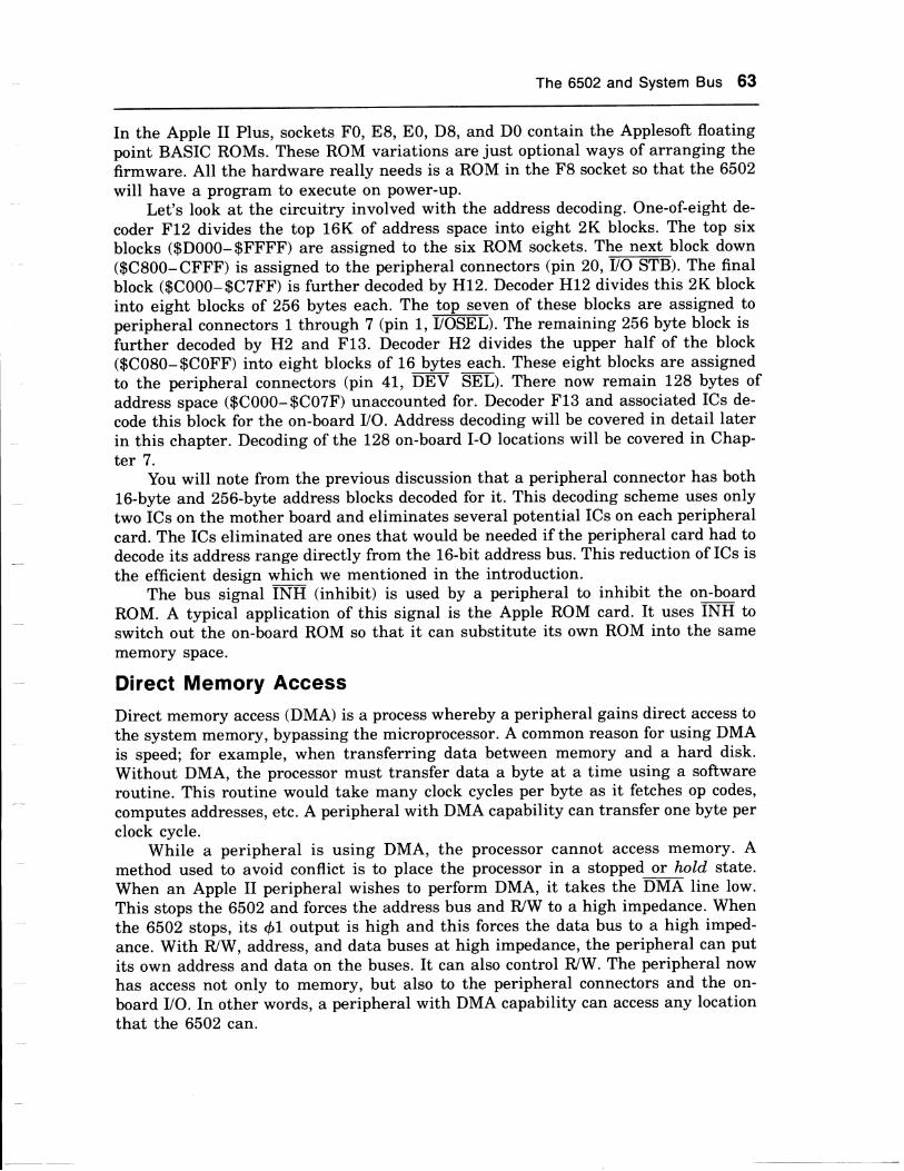
The 6502 and System Bus 63
In the Apple II Plus, sockets F0, E8, E0, D8, and D0 contain the Applesoft floatingpoint BASIC ROMs. These ROM variations are just optional ways of arranging thefirmware. All the hardware really needs is a ROM in the F8 socket so that the 6502will have a program to execute on power-up.
Let's look at the circuitry involved with the address decoding. One-of-eight de-
coder F12 divides the top 16K of address space into eight 2K blocks. The top sixblocks ($D000-$FFFF) are assigned to the six ROM sockets. The next block down($C8QQ-CFFF) is assigned to the peripheral connectors (pin 20, ffi-Sf-Bl. The finalblock ($C000-$C7FF) is further decoded by H12. Decoder H12 divides this 2K blockinto eight blocks of 256 bytes each. The top seven of these blocks are assigned toperipheral connectors 1 through 7 (pin 1,I/OSEL). The remaining 256byte block isfurther decoded by H2 and F13. Decoder H2 divides the upper half of the block($C080-$C0FF) into eight blocks of 16 bytes each These eight blocks are assignedto the peripheral connectors (pin 41, DEV SEt). There now remain 128 bytes ofaddress space ($C000-$C07F) unaccounted for. Decoder F13 and associated ICs de-
code this block for the on-board VO. Address decoding will be covered in detail laterin this chapter. Decoding of the 128 on-board I-O locations will be covered in Chap-ter 7.
You will note from the previous discussion that a peripheral connector has both16-byte and 256-byte address blocks decoded for it. This decoding scheme uses onlytwo ICs on the mother board and eliminates several potential ICs on each peripheralcard. The ICs eliminated are ones that would be needed if the peripheral card had todecode its address range directly from the 16-bit address bus. This reduction of ICs isthe efficient design which we mentioned in the introduction.
The bus signal INE (intribit) is used by a peripheral to inhibit the on-boardROM. A typical application of this signal is the Apple ROM card. It uses INH toswitch out the on-board ROM so that it can substitute its own ROM into the same
memory space.
Direct Memory AccessDirect memory access (DMA) is a process whereby a peripheral gains direct access tothe system memory, bypassing the microprocessor. A common reason for using DMAis speed; for example, when transferring data between memory and a hard disk.Without DMA, the processor must transfer data a byte at a time using a softwareroutine. This routine would take many clock cycles per byte as it fetches op codes,
computes addresses, etc. A peripheral with DMA capability can transfer one byte perclock cycle.
While a peripheral is using DMA, the processor cannot access memory. Amethod used to avoid conflict is to place the processor in a stopped or hold state.When an Apple II peripheral wishes to perform DMA, it takes the DMA line low.This stops the 6502 and forces the address bus and FVW to a high impedance. Whenthe 6502 stops, its {1 output is high and this forces the data bus to a high imped-ance. With R/W, address, and data buses at high impedance, the peripheral can putits own address and data on the buses. It can also control nyw. The peripheral nowhas access not only to memory, but also to the peripheral connectors and the on-board VO. In other words, a peripheral with DMA capability can access any locationthat the 6502 can.

64 Apple ll Circuit Description
Daisy GhainsTheDffi line is connected in common to all peripheral VO connectors. What if morethan one peripheral pulls low onDMA- at the same time? An obvious conflict wouldoccur. A DMA daisy chain is provided that can prevent a bus conflict if used with theproper circuitry. The daisy chain forms a series circuit running through the periph-eral connectors. Circuitry is provided on each peripheral (with DMA capability) tobreak the daisy chain when DMA is requested. The nature of the chain is such thathigher priority is given to peripherals in lower slot numbers. Should two or moreperipherals simultaneously request DMA, only the highest priority peripheral willseize the bus. The exact operation will be described later in this chapter.
There is also a daisy chain for interrupts that can be used for the same purpose
as the DMA daisy chain. Use of the interrupt daisy chain is optional, however, sincea software polting routine could be used to detect and prioritize simultaneous inter-rupt requests.
KeyboardThe keyboard plugs into mother board location A7. When a key is pressed, a 7-bitcode representing that key appears at A7 along with a strobe signal. The strobe isused to set a latch. When the 6502 addresses the keyboard, the seven data bits plusthe latched strobe are driven onto the data bus. The 6502 then reads the data. Iftheprogram finds the strobe bit set, it uses the other seven bits to determine the keypressed. The program also resets the latch to wait for the next character. Fig. 6-4shows the keyboard connector pin assignments at A7.
+5 V
STROBE
RESET
NC
D5
D4
D6
GND
NC
-12VNC
D1
DO
D3
D2
NC
Fig. 6-4. Keyboard connector.
DETAILED CIRCUIT ANALYSIS
6502 Read from RAM
Fig. 6-5 depicts a cycle in which the 6502 reads from RAM. Note that we have shownthe length of a half cycle as it actually is in the Apple-489 nS. This means theApple's 6502 runs about 2Vo faster than the recommended l MHz maximum rate of a
standard-speed part.Tb start the cycle, the 6502 outputs the address during fl. The address becomes
stable by point A. TheDMA is high due to pull-up resistor RA01-3 (Fig. C-9.). Thus,CLL-L1 is low to enable address bus drivers H3, H4, and H5.'lhe address arrives onthe system bus at point B (Fig. 6-5). Since this is a read cycle, 6502 FyW stabilizeshigh at point C. H5-5 is enabled, so BUS F/W goes high at point D. Since we are
addressing RAM in the space 0-48K, one of the inputs of D2 (pins 9, 10, or 12 of Fig.
1 16
2 15
3 14
4 13
5AT.r-6 11
7 10
89
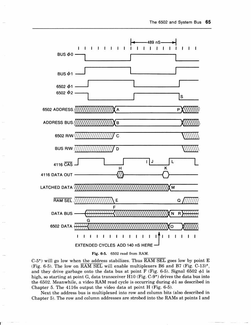
The 6502 and System Bus 65
f--4ae ns ,lll
eus 0o
eus dt
osoz drosoz 6z
6502 ADDRESS
ADDRESS BUS
6502 R/W
BUS R/W
4116CASJ H K
4116 DATA OUr
LATCHED DATA
RAM SEL
DATA BUS
6502 DATA
EXTENDED CYCLES ADD 140 nS HERE
Fig. 6-5. 6502 read from RAM.
C-5*) will go low when the address stabilizes. Thus RAM SEL goes low by point E(Fig. 6-5). The low on RAIVIEEL will enable multiplexers 86 and B7 (Fig. C-13)*,and they drive garbage onto the data bus at point F (Fie. 6-5). Signal 6502 @1 ishigh, so starting at point G, data transceiver H10 (Fig. C-9*) drives the data bus intothe 6502. Meanwhile, a video RAM read cycle is occurring during f1 as described inChapter 5. The 4116s output the video data at point H (Fig. 6-5).
Next the address bus is multiplexed into row and column bits (also described inChapter 5). The row and column addresses are strobed into the RAMs at points I and
r

66 Apple ll Circuit Description
J. The 4116 outputs go low impedance with valid data at point K and the data isheld untilCAS- goes high at point L. Just before it disappears from the 4116 outputs,the data is latched in B5 and 88 (point M). The data is immediately driven onto thedata bus by 86 and 87 (point N). The data then passes through H10 into the 6502(point 0). The F/W and the address are held until point P. Afterahat time, they may.huttg". This change propagates to RANfE:Ef, (point Q). When RAM-SEI goes highat point Q, it disables multiplexers B6 and 87, and the data bus goes high impe-dance (point R). Just before the data is lost from the bus, it is strobed into the 6502on 6502 @2 falling (point S). This completes the cycle.
If this cycle occurs on one of the clock cycles that is extended, there will be anextra 140 nS inserted as shown in Fig. 6-5.
6502 Wlite to RAM
A cycle in which the 6502 writes to RAM is shown in Fig. 6-6. The R/W and theaddresses stabilize during QL at the same time they do during a read cycle. This is awrite cycle, hoggr_ rg_RyW will stabilize low (point A). The Xi./W:tq]gw=g!_A2- (Fig. C-5*), so MIVISEL will be high (point B of Fig. 6-6). When RAM SEL goes
high at point B, multiplexers B6 and 87 (Fig, C-13*) are disabled. This leaves no onedriving the data bus, so it goes high impedance at point C (Fig. 6-6). When BUS 01falls at point D, 4116 WR goes low (point E) due to gate C14-11 (Fig. C-7*). Thisprepares the 4116s for an early-write cycle as described in Chapter 5. When 6502 0Lfalls at point F, it reverses the drive direction of data transceiver H10 via gate C14-8(Fig. C-9*). This reversal lets the 6502 data bus go high impedance (point G of Fig.6-6), and drives garbage onto the system data bus (point H). The 6502 makes its databus low impedance and equal to the write data no later than point I. Data trans-ceiver H10 drives the data onto the system data bus, point J. The data is strobed intothe 4116s on effi falling, point K. The R/W, the address, and the data are held untilabout point L. This concludes the write cycle.
As before, there is a 1 in 65 chance that this cycle could be extended 140 nS.Since this is the case on all 6502 clock cycles, we will not mention it again. We willnote on each figure where the extension would be inserted.
6502 Read from ROM
The timing for a 6502 read from ROM cycle (Fig. 6-7) is similar to the timing for aRAM read cycle. The R/W and the addresses become stable at point A, and there is avideo read during @1 with output at point B. The milfEEf goes high (point C) onBUS d0 rising. This is due to the multiplexing action of @0 at J1-1 (Fig. C-5*). While@0 is low (prior to point C), Jl selects the video address which is always below 32K.Either F2-I2 or F2-11 will be low. Thus, MNI SEL- will be low. When @0 goes highatpointC,J1selectstheaddressbuswhichisabove48Ksinceweare@eROM. None of F2-10, 11, or !2 are low and mMSEf is high. The high on MIVI S-ffidisables 86 and B7 (Fig. C-13*) so they release the data bus (point D of Fig. 6-D.
Right at this same time (00 rising), {1 falls to partially enable decoder F12 viapins 4 and 5 (Fig. C-10*). Since we are addressing above 48K, both ADL4 and ADLSare high. Thus, H1-6 is high to fully enable F12 via pin 6. Decoder F12 now decodes
address lines ADl1, AD12, and AD13 to select one of eight 2K blocks above 48K.Since we are addressing ROM, one of the six F12 outputs assigned to a ROM chipselect will go low (point E of Fig. 6-7). The F12 outputs are assigned to chip selectinput pins 20 and 21. A third chip select pin on each ROM is tied in common to

The 6502 and System Bus 67
f--48e ns rltl
eus Oo
eus dt
o5OZ .7'i L
6502 ADDRESS
ADDRESS BUS
6502 R/W
BUS R/W
RAM SEL
6502 DATA
DATA BUS
4116 ffi
4116 WR
I I r I r I I I I I I I lfr I I I I I
EXTENDED cYcLES ADD 140 nS HERE JFig.6-6. 6502 write to RAM.
signafTNH. It is held high (ROMs enabled) by resistor RA01-?. Address lines ADOthrough AD10 connect to the address inputs of the ROM. These 11 lines select one ofthe 2K locations in each ROM. After the IC's access delays from address and chipselect, the ROM outputs will equal the data contained in the addressed location(point F of Fig. 6-7). This data is driven into the 6502 by H10 (point G). The ROMchip select goes high again on @1 rising, point H. This disables the ROM whichremoves its data from the bus after a short delay, point I. Just before the data disap-pears from the 6502 data inputs (point J), it is strobed into the 6502 on 6502 02falling (point K). This concludes the cycle.
Since the address for this cycle is above 48K, there is no activeTES at point L.It follows that the 4116 outputs remain high impedance at point M, and that thelatched data at point N is garbage.
0( X

68 Apple ll Circuit Description
6502 Read from PeripheralThe cycle for reading from a peripheral is almost identical to the one for readingfrom ROM. We will reuse Fig. 6-7 for our explanation. Peripheral access cycles canbe divided into four categories based on the address decoding:
1. IIO STROBE (Pin 20) -If the address is in the 2k range, $C800-$CFFF,FL2-L4 will go low during O2 (OL low). SignalFI2-L4 is connected in common to nOSTB (pin 20) of all eight peripheral connectors. The typical application for thissignal is to access a 2K ROM on a peripheral card. More than one card can havesuch a ROM, but there must be a method of enabling only one card at a time. Thismethod is described on Page 84 of t}re Apple II Reference Manual under "ExpansionROM:' The ROM decodes the 11 address LSBs and when accessed by 7O Sf-B (pointE of Fig. 6-7), puts the selected data on the data bus. It removes the data on UO StBrising, point H.
2. IIO SELECT (Pin 1) -If the address is in the 2K range, $C000-$C7FF,F12-15 will go low during @2. This partially enables decoder H12 (Fig. C-11*) viapins 4 and 5. Decoder H12 is fully enabled by the high on pin 6 from resistorRA01-8. Next, H12 decodes address bits AD8, ADg, and AD10 to select one of itseight outputs. Each output corresponds to a 256 byte range. The seven high orderoutputs connect to VO SEL (pin 1) ofperipheral connectors 1 through 7. Connector 0has no connection to pin 1. The address range for each connector is $CN00-$CNFFwhere N is the slot number (1-7). The typical application forTO SBL is to access a256 byte ROM on a peripheral card. The ROM decodes the eight address LSBs andwhen accessed by I/O SEL (point E of Fig. 6-7), puts the selected data on the databus. It removes the data on VO SEL rising, point H.
3. DEVICE SELECT (Pin 41) -The low order output from H12 (pin 15) will golow during O2 if the address is in the range $C000-$C0FF. This low will partiallyenable H2 via pin 4. Decoder H2 is also partially enabled during 62by the low (@1)
on pin 5. Finally, H2 will be fully enabled when AD7 (H2-6) is high. This corre-sponds to the range $C080-$C0FF. Next,IC}J2 decodes address bits AD4, AD5, andAD6 to select one of its eight outputs. Each output corresponds to a 16 byte rangeand connects to DETSEI (pin 41) of the peripheral connectors. The address rangefor each connector is $C0N0-$C0NF where N is the slot number plus 8 (that is N :g8 to gF). The typical application for DEV S-Ef, is to access assorted latches, regis-ters, UARTs, etc., on a peripheral card. The card decodes the four address LSBs andwhen accessed by DEVSEL (point E of Fig. g-f), puts the selected data on the databus. It removes the data on DEV S-EL rising, point H.
4, Full Address Decode-A peripheral card does not have to use the decodedaddress on pins L,20, and 41. The card can perform its own decoding ofthe addressbus (AD0-AD15). An application would be a card that is addressed in a range notavailable on pins 1,20, or 41. For example, the Apple ROM card responds to therange $D000-$FFFF; not available as a predecoded select line. Note that the ad-dress bus becomes stable (point O) before the decoded select lines (point E), an ad-vantage of this decoding method. However, the peripheral should still wait until @1is low to output to the data bus. This is to avoid a bus conflict since 86 and B7 drivethe bus until point D.
A Caution for Designers-A few words about the read data hold time are inorder. They apply to all four addressing methods discussed previously. The 6502data sheet specifies that at the end of a read cycle, the data must remain stable onthe 6502 data inputs for a 10 nS hold time after 6502 S2 falling. Referring to Fig.
I-

The 6502 and System Bus 69
l--4ae ns rl
eus do
eus dt
osoz dr6502 6Z
6502 ADDRESS
ADDRESS BUS
6502 R/W
BUS R/W
4116 cTsB
4116 DATA OU'
LATCHED DATA
tro
RAM SEL
ROM CHIP SELECT,l ra (PtN 2o),
t/o sEL (PlN 1), ORDEV SEL (PlN 41)
DATA BUS
6502 DATA
I I I I I I I I I I I I ltlEXTENDED CYCLES ADD 140 nS HERE J
Fig. 6-7. 6502 read from ROM or peripheral.

70 Apple ll Circuit Description
6-7, we see that point J (6502 data no longer valid) must occur at least 10 nS afterpoint K (6502 02 falling). Recall that 6502 @2 is not used in the Apple II. The signalthat is used in its place to enable data onto the bus is BUS @0.
BUS 00 leads 6502 02 by the propagation delays through B11-3 and the 6502.Thus, when BUS 00 goes low to remove the data from the bus, it may remove thedata before the 6502 hold time has been satisfied. This problem can be helped byusing reTTB, TOSEL, DE-VSE-f,, or inverted @1 instead of @0 to enable the dataonto the bus. Also, the use of a data bus buffer that is slow to disable will help. Insummary, the designer of an Apple II peripheral card should make a careful timinganalysis.
6502 Wlite to PeripheralA cycle in which the 6502 writes to a peripheral (Fig. 6-8) is similar to a cycle inwhich it reads from a peripheral. On a write cycle, R/W will stabilize low (point A)and RAM SEL will stabilrze high (point B). When RAlfSEtable 86 and 87 (Fig. C-13*), releasing the data bus at pointffiB; rc-S-[, orffiwill go low (point D). Also on OLlow (point E). This does nothing, however, since there is no4LI6 WR is active.
On 6502 {1 falling, data transceiver H10 (Fig. C-9*) reverses its drive direction.This releases the data bus toward the 6502 (point F of Fig. 6-8) and drives garbageonto the system data bus (point G). The peripheral card is selected by I/O-EB, I/OSEL-, DEVEEL, or a full decoding of the address bus. It then waits for the write dataof the 6502 to become valid and driven onto the data bus, point H. The peripheralcard should strobe the data into its memory or registers on the rising edge of UOStB, TO.S-E-L, DEVEEL (point I), or @1 (point J). This completes the write cycle.
6502 Read from KeyboardIn our discussion of the peripheral address decoding, we determined that HL2-L5(Fie. C-11*) goes low during @2 when the address is in the range $C000-$C0FF.This low partially enables decoder F13 via pin 5 (FiS. C-12*). Decoder F13 is furtherenabled via pin 6 when {0 is high. Decoder F13 is finally fully enabled via pin 4when AD7 is low. This corresponds to the 128 byte address range $C000-$C07F.Next, F13 decodes address bits AD4, AD5, and ADG to select one of its eight outputs.Each output corresponds to a 16 byte range. The low order output (pin 15) is ofinterest to us here; it is the signal RBD-KBD will go low during Q2 if the addressis in the range $C000-$C00F. When programming, we simply use $C000.
Fig. 6-9 shows a cycle during which the 6502 reads the keyboard. (It is similarto Fig. 6-'7, a cycle during which the 6502 reads from ROM.) The 6502 puts out thekeyboard address at point A and takes F/W high at point B. When R/W goes high,RAM SEL goes low (point C). When f0 goes high at point D, multiplexer J1 switches(Fig. C-5.). Since we are addressing above 48K, D2 pins g, 10, and L2 all go high.This would normally take FAME-L high. We are addressing the keyboard, how-ever, so on f0 rising, KBD goes low (point E of Fig. 6-9). A low KBD signal at D2-13makes D2-8 high and keeps mil[SEf low (point F). Thus, RBD low at multiplexersBG and 87 (pin 1) causes them to select the keyboard connector A7 (Fig. C-13*).(Data bits 0-6 go to the connector; bit 7 is the latched keyboard strobe, 810-9.) WithRAM SEL low at BG and 87 pin 15, they drive the keyboard data and strobe onto the
goes high, it will dis-C. On OL falling, ID
falling,4-1L6 WR goes4LL6 CAS while this

The 6502 and System Bus 71
l*-48g ns--+l
eus do
eus dr 'osoz 0r
0( I/O ADDRESS )6
4116 WR
6502 ADDRESS
ADDRESS BUS
6502 R/W
BUS R/W
+rro ffiVIDEO
4116 DATA OUr
RAM SEL
6502 DATA
DATA BUS
l/OSEL(PlN1),T^ t-l/o sTB (PtN 2O), ORDEV SEL (PlN 41) I'a r r r r r r r r I r r ttr t I I I
IEXTENDED CYCLES ADD14O NS HEREJ
Fig. 6-8. 6502 write to peripheral.
data bus, point G. Data transceiver H10 drives the data into the 6502 which strobesit on 6502 S2 falling, point H. This concludes the keyboard cycle.
When any character key is pressed on the keyboard, A7-2 goes high (FiS. C-13*).This sets flip-flop B10 and its pin 9 goes high. When a program scans or reads thekeyboard, it checks data bit 7 (810-9). A 1 (hieh) indicates that a key has beenpressed and that data bits 0-G contain the character. The program must then ad-dress location $C010. This takes eIE-Sm low and clears 810-9 via C11-4 andA12-1. If this is not done, 810-9 will still be high on the next scan, and the samecharacter will be read again.
I/O ADDRESS

72 Apple ll Circuit Description
f*-48e ns ,lttttttttt ttttttttt
eus 6ocr\rg vrv
eus dt
osoz drasoz Qz
6502 ADDRESS
ADDRESS BUS
6502 R/W
BUS R/W
A $cooo x{
fr $cooo )fi
+'o cTsVIDEO
4116 DATA OUt
LATCHED DATA
RAM SEL
KBD
DATA BUS
6502 DATA
rrttttttttttEXTENDED CYCLES ADD 140 nS HERE
Fig. 6-9. 6502 read from keyboard.
USER 1
A signal named USER 1 is connected in common to pin 39 of all eight peripheralconnectors (Fig. C-11*). USER 1 then connects to a jumper on the mother board.When this jumper is absent, USER L can be used as a signal line between two ormore peripheral cards. Its application would be up to the designer of the peripherals.
G KBD DATA

The 6502 and System Bus 73
When the jumper is installed, USER 1 connects to H12-6. This gives the peripheralscontrol over the 2K address space $C000-$C7FF. This range consists of the on-boardUO and the memory blocks selected by ?OTE.[ and Dffiffi. When USER ]. ishigh, this range is not affected. When USER 1 is low, the range $C000-$C7FF isinhibited.
The Ready LineThe RDY (Ready) line gives the peripheralthe 6502 an integer number of clock cycles.ripheral devices with long access times.
cards the ability to momentarily delayAn application would be the use of pe-
Fig. 6-10 depicts a read cycle that has been extended by one wait state. The basiccycle is similar to the read from peripheral shown in Fig. 6-7. The main differenceoccurs when the peripheral takes RDY low to indicate that it will not have dataready within the usual one cycle. This occurs during S1 after the peripheral recog-nizes its address, between points A and B in Fig. 6-10. DurirLg Q2, the 6502 willsample RDY and see that it is low. As a result, the 6502 will not strobe in the dataat the end of {2. Instead, it maintains R/W and the address for another clock cycle.Our peripheral is ready now, so during @1 of the second cycle (points C to D) itreleases RDY. Resistor RA01-5 pulls RDY high (Fig. C-9*). The 6502 again samplesRDY during S2 and., seeing that it is high, completes the read cycle.
The peripheral card can start decoding the address as early as point E (Fig.6-10). However, it should not drive the data bus unless iffiB,I/O-SET, DE-VSffi,or @1 is low. This is to avoid a bus conflict with multiplexers B6 and 87. Note thatany number of wait states may be inserted to extend the cycle. With the appropriatecircuitry, RDY can be used to single step the processor one clock cycle at a time.
DMA Daisy ChainWe introduced the concept of DMA in the overview. The DMA allows a peripheralcard to gain direct access to the system bus and take over in place of the 6502. Onlyone card at a time can be allowed to do this. Fig. 6-11* shows the DMA daisy chainthat allows access to the bus, one card at a time, on a priority basis. We have showncards with DMA capability plugged into slots 0, 2, and 7. The card plugged into slot1 does not have DMA capability. A line on this card simply connects DMA ItrI (pin27) to DMA OUT (pin 24).
The daisy chain starts at slot 0 pin 27 and. continues through the cards and themother board to slot 7 pin 24. T}rre DMA OUT from slot 7 (pin 24) goes nowhere andis a don't care. (The optional connection at solder pad "7," Fig. C-11*, is not associ-ated with DMA.) The DMA IN at slot 0 also has no connection on the mother board.Although not shown in this example, slots 3 through 6 must contain cards so thatthe daisy chain will be continuous. You do not need eight cards to use DMA. If youhave fewer cards, they must be arranged so that the chain is continuous. The chainneed not start in slot 0 or end in slot 7. The cards with higher priority are placedtoward slot 0.
Normally, the signal CHAIN on each card is high. A pull-up resistor is providedon each card so that DMA IN of the highest priority card will be high. As a result,the daisy chain is normally high all along its path.
For DMA operation, suppose the card in slot 2 needs to perform a DMA. Thelogic on the card checks DMA IN and finds it to be high. This "tells" the card it mayproceed since no higher priority card needs DMA. The slot 2 card then takes CHAIN

74 Apple ll Circuit Description
f++as ns+|tt I tttt ttt I tltt I tt tltttttt tttt tttt
BUS O.|
OR
VIDEO VIDEO
DEV SEL
RDY
DATA BUS
6502 DATA
I tttt tt tttttttttt tttl I I I I I I I I ttt ttl*-wAlr STArE rf r REAo-l
Fig.6-f0. 6502 read from peripheral extended by ready line.
low with the result that DMA OUT goes low. This low will propagateto lower priority cards, preventing them from starting DMA cycles.
down the chainThe slot 2 cardit removes thealso takes DMA low via an open collector gate. When DMA is low,
6502 from the bus-more on this later.Now suppose a higher priority card (slot 0) needs to perform a DMA. Slot 0
BUS OO
6502 016502 62
6502 ADDRESS -1ffi
ADDRESS BUS
6502 R/W
BUS R/W
4110 il-S
4116 DATA OUT
RAM SEL
rffis,iffi-EL,
XE

The 6502 and SYstem Bus 75
DMA IN is high, so the card in slot 0 proceeds. It takes CHAIN and DMA OUT low.
This low propagates to slot 2 where it prevents that card from performing a DMA.
fhe b1t.q operation must be synchronous. This means that peripheral cards
must get their timing from the system clocks and start DMA cycles only during 01.Otheiise, a peripheial could cut short a 6502 cycle and higher priority peripherals
could cut short cycles of lower priority peripherals.
DMA Read from RAMFig. 6-12 shows a DMA read from RAM followed by a 6502 read from RAM. On @1
"ir"itrg (point A), the peripheral card checks DMA IN (point B). The DMA IN is high,
978nS#tllllllll ll I | | ll ll I ll! lll lllllll
BUS dO
BUS 016502 0o
6502 0t6502
ADDRESS
ADDRESSBUS
6502 R/W
BUS R/W
4110 il-s41 16DATAOUT
LATCHEDDATA
o-@aQVIDEO
\
DMA VIDEO
\
6502
\
RAM SEL
DATABUS
6502DATA
DMA
V 6502 ADDRESSE DMA ADDRESS
DMA IN
DMA OUT
F-DMA READ cyclE-+-f-6502 READ cYcLE-l
ttrlllllllllllllllllFig. 6-12. DMA read from RAM.

76 Apple ll Circuit Description
so the card takes DMA low (point C) and DMA OUT low (point D). It also drives anaddress onto the bus (point E) and takes F/W high (point F). The DME low at C11-13takes CLL-I? high to disable bus drivers H3, H4, and H5 (Fig. C-9). Thus, the 6502address and F/W are removed from the bus so they will not conflict with the DMAaddress and R/W.
This is a RAM read cycle, so EAIISEL- goes low as soon as the DMA address isdecoded on the mother board (point G of Fig. 6-L2). The 6502 address and F/W be-come valid at points H and I, but have nowhere to go yet.does not interfere with the video read from RAM at pointwill keep 6502 f0 low all the way from point K to point L.as if its clock input had stopped. The 6502 will hold its OI
Note that the DMA cycleJ. The DMf low at 811-1It will appear to the 6502output high from point M
to point N and will not enter @2 until point N.At point O, the +f fO eAS goes low for the memory bank selected by the DMA
address. The data becomes valid at point P and is latched at point Q. It is drivenonto the data bus by 86 and 87 (Fig. C-13*) at point R. The peripheral card shouldstrobe in the data on @1 rising at point S. Also on {1 rising, the card returns DMAand DMAIUT high (points T and U).
With DMA now high, H3, H4, and H5 (Fig. C-9.) are enabled and drive the 6502address and F/W onto the bus (points V and W of Fig. 6-12). Gate 811-3 now lets the6502 clock continue and the 6502 enters 62 at point N. The 6502 read from RAMcontinues as previously described.
DMA Write to RAM
Fig. 6-13 shows a DMA write to RAM cycle followed by a 6502 read from RAM. TheDMA write operation is very similar to the DMA read cycle just described. Since thiswill be a write cycle, the first difference occurs when the peripheral card takes busF/W low (point A). Bus F/W will cause mN[SEf to be high, point B. The card alsodrives the data to be written onto the data bus, point C. Since bus H/W is low, 4116WE will go low at point D. The 4116 eAS goes low at point E to strobe the DMAdata into RAM. Note that 6502 +I is high from point F to point G. As a result, C14-8(Fig. C-9*) is high to keep data transceiver H10 from driving the data bus andconflicting with the DMA write data.
On @1 rising (point H), the card releases DN[A, bus Rl/W, the address bus, andthe data bus. The 6502 read from RAM cycle that follows has been previously de-scribed.
Note that Figs. 6-12 and 6-13 show simple examples of DMA cycles. Variationsand refinements are possible. Also note that peripheral cards can have direct access
to much more than memory. We showed DMA cycles that read and write the RAM.A card can also access ROM, on-board UO, and other peripherals. It can performreads or writes as appropriate. We have shown 6502 read from RAM cycles followingthe DMA cycles in Figs. 6-12 and 6-13. Of course, any cycle type could have followed,including another DMA from the same or a different card.
Recall that part of the DMA process involves stopping the @0 clock input of the6502. The 6502 is a dynamic device. If its clock input is stopped for too long, it willlose the data in its internal registers. Thus, a peripheral DMA device cannot holdthe DMA line low continuously. The DME line must be released at 10 p,S minimumintervals so.that the 6502 can refresh itself. Note that 10 pS is the most restrictiuevalue obtained from the 6502 data sheets (References 6.9,6.12, and 6.15 in AppendixD).
AS
in

The 6502 and System Bus 77
*e7BnSltttlltll tl r l l l r r lllr rr l tr I llll
BUS OO
BUS 016502 0o
6502 (0 1
ADSflg1s\
ADBtEsss
6502 R/W
BUS R/W
4116 WR
4110 CnS41 16DATAOUT
LATCHEDDATA
VIDEO VIDEO
C DMA WRITE DATA
RAM SEL
DATABUS
6502DATA
DMA
I tt rr r I ll ll ll ll I llll llllllllllll
!-DMA WRTTE CycLE 6502 READ Cy6r-e+lFig. 6-13. DMA write to RAM.
lnterruptsInterrupt Daisy Chain-Interrupts of the 6502 microprocessor were discussed in
the overview of this chapter. There we mentioned that an interrupt daisy chain wasavailable that could be used to prioritize interrupt requests. This interrupt daisychain operates just like the DMA daisy chain shown in Fig. 6-11*. Just substituteINT IN (pin 28) and INT OUT (pin 23) for DMA IN and DMA OUT. Also substituteIRQ or NMI for DMA. (Note: The optional connection at solder pad "8," Fig. C-11*, isnot associated with interrupts.)
6502
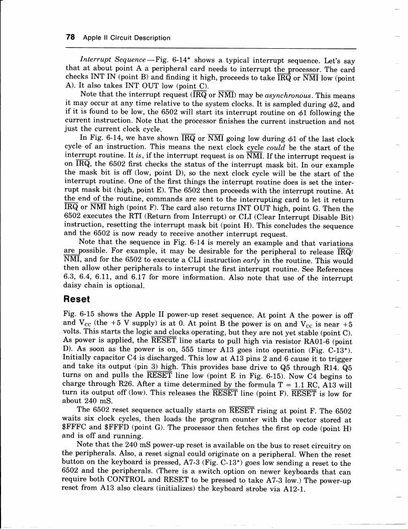
78 Apple ll Circuit Description
Intercupt Sequence-Fig. 6-L4* shows a typical interrupt sequence. Let's saythat at about point A a peripheral card needs to interrupt the processor. The cardchecks INT IN (point B) and finding it high, proceeds to take IRQ or IriMI low (pointA). It also takes INT OUT low (point C).
Note that the interrupt request (IEQ or illNfD may be asynchronozs. This meansit may occur at any time relative to the system clocks. It is sampled during e2, and,if it is found to be low, the 6502 will start its interrupt routine on {1 following thecurrent instruction. Note that the processor finishes the current instruction and notjust the current clock cycle.
In Fig. 6-14, we have shown IRQ or I\IMI going low during dl of the last clockcycle of an instruction. This means the next clock cycle could be the start of theinte_rrupt routine. It is, if the interrupt request is on IriMI. If the interrupt request ison IRQ, the 6502 first checks the status of the interrupt mask bit. In our eiamplethe mask bit is off (low, point D), so the next clock cycle will be the start of theinterrupt routine. One of the first things the interrupt routine does is set the inter-rupt mask bit (high, point E). The 6502 then proceeds with the interrupt routine. Atthe end of the routine, commands are sent to the interrupting card to let it returnIRQ- or IIMI trigh (point F). The card also returns INT OUT h[h, point G. Then the6502 executes the RTI (Return from Interrupt) or CLI (Clear Interrupt Disable Bit)instruction, resetting the interrupt mask bit (point H). This concludes the sequenceand the 6502 is now ready to receive another interrupt request.
Note that the sequence in Fig. 6-14 is merely an example and that variationsa_le.lossible. For example, it may be desirable for the peripheral to release lil(/NMI, and for the 6502 to execute a CLI instruction early in the routine. This wouldthen allow other peripherals to interrupt the first interrupt routine. See References6.3, 6.4, 6.11, and 6.17 for more information. Also note that use of the interruptdaisy chain is optional.
ResetFig. 6-15 shows the Apple II power-up reset sequence. At point A the power is offand Vsg (the +5 V supply) is at 0. At point B the power is on and Vgg is near *bvolts. This starts the logic and clocks operating, but they are not yet stable (point C).As power is applied, the ffiET line starts to pull high via resistor RA01-6 (pointD). As soon as the power is on, 555 timer A13 goes into operation (Fig. C-lg*).Initially capacitor C4 is discharged. This low at A13 pins 2 and,6 cause it io triggerand take its output (pin 3) high. This provides base drive to Q5 through R14- Qsturns on and pulls the RE-SE-F line low (point E in Fig. O-lb). Now CZ begins iocharge through R26. After a time determined by the formula T : 1.1 RC, Atg willturn its output off (low). This releases the RESE-T line (point D. RES-ET is low forabout 240 mS.
The 6502 reset sequence actually starts on ffiET rising at point F. The 6b02waits six clock cycles, then loads the program counter with the vector stored at$FFFC and $FFFD (point G). The processor then fetches the first op code (point H)and is off and running.
Note that t}ae 240 mS power-up reset is available on the bus to reset circuitry onthe peripherals. Also, a reset signal could originate on a peripheral. When the resetbutton on the keyboard is pressed, A7-3 (Fig. C-13*) goes low sending a reset to the6502 and the peripherals. (There is a switch option on newer keyboards that canrequire both CONTROL and RESET to be pressed to take A7-3 low.) The power-upreset from AlB also clears (initializes) the keyboard strobe via 412-1.

The 6502 and System Bus 79
lL tsvo58sftd9Ho=
ztL r-O
><o zFC) ur H C->
edtaob -o,
ZFI
-,23z
a:fd)aaLUE,oo
5@fdl
olcL_6lil
Ogafcl
l= [tlz ralE SY
ei3
l-aEtr
Fig. 6-14. 6502 interrupts.

80 Apple ll Circuit Description
c
oo ffimlV..
tuf*--- 240 mS-*f
Fig. 6-15. 6502 reset sequence.
6502 'Scope LoopIn this chapter we have presented an assortment of processor cycles: RAM read,RAM write, ROM read, keyboard read, etc. For each one we have examined a timingdiagram that shows just that one cycle. The waveforms look nice when printed onpaper, but what do they look like on an oscilloscope?
Viewing microprocessor cycles on an oscilloscope is a bit tricky. It is not assimple as looking at a clock or a video waveform. Clocks, for example, are repetitiveand follow a sequence that is defined by the way the hardware is wired. The signalsfrom a microprocessor, on the other hand, are determined by the program that isrunning.
If we want to examine the timing of a specific 6502 cycle, we can use a shortprogram called a'scope loop.In the program we put instructions that contain thecycle types we want. For example, if we wanted to examine the timing of a RAMread followed by a peripheral write, we could use an STA-absolute instruction. Thisinstruction is four clocks long and consists of three reads followed by a write. Sincewe specified a read from RAM, our'scope loop would have to execute in RAM. Sincewe specified a write to a peripheral, the address in the instruction would have to bein the peripheral's address space. The 'scope loop is made short so the waveformswill have a high repetition rate and be easily seen on an oscilloscope.
The program below is a short loop that can be run on the Apple II. It allows usto view several types of 6502 cycles as listed in the comments.
RESET
ADDRESSBUS
DATA BUS
0800 AD30c0 LooP0803 AD00c00806 AD00F80809 8D00090812 4C0008
oRG $8ooLDA $C030LDA $C000LDA $F8OOsTA $e00JMP LOOP
;SCOPE LOOP.;
;TOGGLE SPEAKER;READ KEYBOARD;READ PROM;WRITE TO RAM;NOTE: ANY OP CODE FETCH;IS A READ FROM RAM;TOTAL _
CLOCKCYCLES:
44443
19
The results of the program are shown in Fig.6-16*. The first instruction (LDA$C030) tells the processor to load its accumulator with the data found at location
$FFFC$FFFD H
The 6502 and System Bus 81
$C030. Location $C030 is the address assigned to the on-board speaker. Wheneverwe access that location, the speaker toggles. We do not care that the speaker does notreturn any data; we are using the LDA instruction merely as a means to generatethe address.
This instruction consists of four clock cycles. The first three cycles read the opcode and its operand from consecutive RAM locations. These locations ($800, $801,and $802) are shown in Fig. 6-16* on the address bus. At location $800, the op code($AD) is read from RAM as shown on the 4116 DATA OUT trace. This data is thenlatched, put on the data bus, and finally put on the 6502 data lines. At location $801,the operand low order byte ($30) is read. The high order byte ($C0) is read fromlocation $802.
On the fourth cycle, the processor performs the operation specified by the opcode. It first outputs $C030 on the address bus (point A). This is decoded on themother board and found to be above 48K. Thus, there is no 4116GS, andEN[Etgoes high during d2 (point B). The address is further decoded by the string of decod-ers F12, H12, and F13 (see Figs. C-10*, 11*, and 12*). The specific address $C030causes F13-12 to go low during d2 (point C of Fig. 6-16*). The rising edge of F13-12causes flip-flop J13-5 to toggle and create a sound in the speaker (point D). More onthis in Chapter 7. Notice that the speaker does not respond with any data, so thedata bus goes high impedance during @2 (point E). The resulting garbage on thedata inputs of the 6502 is strobed on S2 falling at the end of the cycle. Rememberthat we do not care about this data anyway.
You will notice the video cycles (indicated by a "V") interleaved with the 6502cycles throughout Fig. 6-16*.
If you were to actually enter the 'scope loop program (or any other program) intothe Apple and view the processor signals on an oscilloscope, you would see the effectof the extended clock cycles. This is a messy display that could cause confusion. Tbeliminate the extended cycles, lift IC D2 pin 6 (Fig. C-2*). Everything except colordisplays should continue to operate properly, and you will get cleaner oscilloscopedisplays.
If you wish to view one complete period of the loop, you need to trigger theoscilloscope on a signal that occurs once each period. You could use F13-12 (Fig.C-L2*) in our example.
Let's return to Fig. 6-16* and discuss the remaining instructions. The secondinstruction (LDA $C000) is similar to the first. Notice that the RAM locations for theop code and its operand start at $803 which follows the last address used by theprevious op code. In the fourth cycle of this instruction we address the keyboard($C000) which does respond with data (point F).
The third instruction (LDA $F800) is similar to the first two. Here we load thefirst byte from the monitor ROM ($4A) into the accumulator.
The fourth instruction (STA $900) tells the processor to store the contents oftheaccumulator at location $900. The first three clock cycles of this instruction fetch theop code ($8D) and its operand ($900) from RAM locations $809, $810, and $811. Onthe fourth cycle, the 6502 takes F/W low (point G). When B/W goes low, RAM SELgoes high. Since R/W is low, 4116 WR goes low during d2 (point H). Later during @2,the 6502 outputs the contents of its accumulator ($4A obtained in the previous in-struction). The data is strobed into the RAM on 4116TfS falling during d2 (point I).
The fifth and last instruction is JMP $800. This tells the processor to jump tolocation $800 and execute the op code found there. Since $800 is the beginning of theprogram, the loop repeats.

82 Apple ll Circuit Description
GNDDMA IN
INT INffiTm-RESiffi
-12V-5V
COLOR REF7M
Q30r
USER 1
doDEVICE SELECT
D7D6D5D4D3D2D1
DO
+12 V
+5VDMA OUTINT OUTDfrMRDYI/O STROBESYNCR/W415A14A13412A11A10A9A8A7A6A5A4A3A2A1AOffiNOTES:
26
27
28
29
30
31
32
33
34
35
36
37
38
39
40
41
42
43
44
45
25
24
23
22
21
20
19
18
17
16
15
14
13
12
11
10
II7
6
5
4
3
2
1
46
47
48
49
50
SLOT 7 ONLY
SLOTS 1-7 ONLY
FRONT
Fig. 8-17. Peripheral connector pinout. (Courtesy Apple Computer, Inc.)

The 6502 and SYstem Bus 83
Table 6-1 The ApPle II Bus
PinNumber
Siqnalnime tr
Modetr Description
1 rcrt INPUT/OUTPUT SELECT. Seven individually decodedlines for slots 1-7. ireE at any one connector goes
low during 02 when $CNOO-$CNFF is accessed; N -slot number.
2-17 ADO-AD1 5 B 16-bit address bus. Address becomes valid during 01and remains valid throughout +2.
18 R/W B READ/WRITE. Becomes valid during 01 and remainsvalid throughout 02. High for read; low for write.
19 SYNC Video synchronization signal (C13-8). Connects to slot7 only.
20 UO STB I INPUT/OUTPUT STROBE. Common select line thatgoes low during O2 when $C800-$CFFF is accessed.
21 RDY B READY. Taken low during O1 to insert wait states. The6502 recognizes low on RDY only during read cycles.
22 DINA o DIRECT MEMORY ACCESS. Taken low at the begin-ning of ,f1 to halt the processor and make the address,data, and R/W lines high imPedance.
23 INT OUT o INTERRUPT OUT. Daisy chain to lower priority slots.Normally driven high if used; connects to pin 28 if notused.
24 DMA OUT o DIRECT MEMORY ACCESS OUT. Daisy chain to lowerpriority slots. Normally driven high if used; connectsto pin 27 if not used.
25 +5V + 5 volts
26 GND Ground
27 DMA IN DIRECT MEMORY ACCESS lN. Daisy chain input fromhigher priority slots. Normally high.
28 INT IN I INTERRUPT lN. Daisy chain input from higher priorityslots. Normally high.
29 NMI o NON-MASKABLE INTERRUPT. Taken low to start a6502 non-maskable interruPt.
30 mo o INTERRUPT REQUEST. Taken low to start a 6502maskable interrupt. Recognized only if interrupt dis-able flag is not set.
31 RESET B As an output, taken low to reset the 6502 and otherperipherals. As an input, goes low during resets fromthe keyboard, oD power-up, and from other peripher-als.

84 Apple ll Circuit Description
Table 6-1 -cont. The Apple ll BusPinNumber
Siqnalttime tr
Modetr Description
32 INH o lNHlBlT. Taken low to inhibit the ROM address space($Dooo-$FFFF).
33 -12 V 12 volts
34 -5V -5 volts
35 COLOR REF I COLOR REFERENCE. Connects to stot T onty.
36 7M I 7MHz. 7.15909 MHz clock.
37 Q3 2.040968 MHz (average) clock.
38 01 I PHASE 1. 1.020484 MHz (average) system ctock.Used on bus in place of 6502 01 .
39 USER 1 o Taken low to inhibit the llo address space($cooo-$c7FF).
40 00 PHASE 0. 1.020484 MHz (average) system clock andcompliment of O1 . Used on bus in place of 0502 02.
41 DEV SEL I DEVICE SELECT. Eight individually decoded selectlines, ohe for each stot.ffi at any one connectorgoes low during O2 when $COXO-$C0XF is accessed;X:N+8,N_slotnumber.
42-49 D7-DO B Eight bit bidirectional data bus. Data becomes validduring 02 and remains valid to the end of 02.
50 +12 V + 12 volts
Notes: Unless otherwise specified, all signals appear on all eight connectors.
l: lnput With respectO: Output to peripheralB: Bidirectional card.
There are 19 clock cycles in the loop, giving a period of 19 x 978 nS : 18.bg pS.However, if an extended clock cycle falls during a period of the loop, then that periodwill be 18 x 978 nS + 1117 ns : t8.72 ps. Note the slight difference.
The extended clock cycles produce some subtle effects. We have just demon-strated the first effect. That is, if you are using a sequence of processor instructionsto produce a short and precise delay, an extended cycle will increase your delay by140 nS. A second effect was discussed in Chapter 3; extended cycles decrease theprocessor's speed from 1.023 MHz to 1.020 MHz. This slight difference would havean effect on the computation time of uery long calculations.
A third effect arises since the processor clock is not a pure frequency-it has aL5.7 kIJ:z component. Tb demonstrate this effect, consider our 'scope loop. It has anaverage period of 19 +1.020 MHz : 18.63 g,S. Each time through the loop thespeaker is toggled. A complete period of speaker cone movement requires two passesthrough the loop. This period is 37.3 pS. The frequency is 26.8 kHz-too high to
trtr
F

The 6502 and System Bus 85
hear. Yet when you run the 'scope loop, you dospeaker. What you hear is the beat betweencomponent-this is 11.1 kHz, clearly audible.
SUMMARY
This chapter concludes with a summary of the Apple II bus. A brief review of eachsignal is given in Thble 6-1. Fig. 6-17 shows the physical arrangement of the bus onthe peripheral connectors.
In the next chapter we will examine the on-board VO and the soft switches.
hear a high pitched sound from the26.8 kHz and the I5.7 kHz clock

CHAPTER
On-Board Il O
A computer is of little use unless it communicates with the outside world via its VOfacilities. Minimum UO usually consists of a keyboard for input and a crt display foroutput. Some computer architectures require plug-in peripheral boards to provideany UO, including this minimum set. In the Apple II, many of the frequently usedVO devices are located on the mother board. This built-in VO contributes to yourability to just plug in the Apple II and start computing.
In this chapter we cover the built-in or on-board IJO. This includes the cassetteVO, the game port, the speaker, and the keyboard.
Schematic Reference: Figs. C-12*, C-13*, and. C-22*.
OVERVIEW
In Chapter 6 we mentioned that the address range $C000-$C07F was used for theon-board VO. This range is decoded by ICs FL3 and F14 (Fig. C-12*). There are nineinputs and 13 outputs listed as follows:
lnputs OutputsKeyboardCassette TapeGame Switches O-2Game Paddles 0-3
Clear Keyboard StrobeCassette TapeSpeakerGame Paddle TriggerGame Utility StrobeGame Annunciators 0-3TEXT Soft SwitchMixed Mode Soft SwitchPage 2 Soft SwitchHIRES Soft Switch
KeyboardThe built-in keyboard consists of two printed-circuit boards. On one board aremounted thLe 52 keys. On the second board are mounted five ICs and assorted dis-
86

On-Board llo 87
crete components. Keyboard encoder IC 86 scans t}re 47 character keys looking forone that is depressed. These 47 keys are arranged in a 9 by 10 matrix as shown inFig. C-22*. Not every point in the matrix is occupied by a key. This matrix ar-rangement allows BG to detect a key closure using only 19 instead of 47 pins. WhenBG detects a depressed key, it generates the corresponding ASCII character at itsoutput. If the SHIFT key, CTRL key, or both are also depressed, 86 generates theASCII character for a shift, control, or shift-control function. The output of 86 isbuffered by 85 and B4-3 then connects by a short flat cable to A7 on the motherboard.
Timer IC B2 is connected to oscillate at about 15 }Jz.It provides a repeat strobeto B3-3 when the REPT key is depressed. The RESET key connects directly via theflat cable to A7 on the mother board. Note that the SHIFT, CTRL, and REPT keys donot generate characters unless used with another key. The RESET key also does notgenerate characters since it connects directly to the 6502.
Cassette Tape
The Apple II can store and retrieve digital data using a standard audio cassette taperecorder. The hardware involved is fairly simple; all the intelligence is in thefirmware. When you store a program, routines in the monitor ROM cause flip-flopJ13-9 (Fig. C-12*) to generate square or rectangular waveforms. Thus, J13-8 thendrives the CASSETTE DATA OUT jack. This jack is meant to be connected to themicrophone input of the recorder.
The earphone output of the recorder connects to the CASSETTE DATA IN jackof the Apple. When you load a program, the signals from the tape pass throughoperational amplifier K13, then appear at an input of data selector H14. The 6502can read the output of H14 under program control. The program (again in themonitor ROM) then processes the cassette signal to reproduce the data.
SpeakerTbnes are produced in the speaker of the Apple by toggling flip-flop J13-5 underprogram control. Transistor Q4 amplifies the output of J13-5 to drive the speaker.
Game GonnectorSeveral of the on-board inputs and outputs appear at connector J14 (Fig. 7-1). Al-though J14 is called the "game connector," it can have other applications.
Up to three switches can connect to the J14 pins named SWO, SWl, and SW2.
+5 VSWO
SW1
SW2
STE
PDLO
PDL2
GND
N.C.
ANO
AN1
AN2
AN3
PDL3
PDLl
N.C.
1 16
2 15
3 14
4 J14 13
5126 11
7 10
89
Fig. 7-1. Game connector.

88 Apple ll Circuit Description
The 6502 can select and read the switches via H1a (Fig. C-t2*).In the game appli-cation, the switches are usually momentary-operate push buttons.
Up to four variable resistors can connect to Jl4 at the pins named PDLQ-PDL$.These external variable resistors control the timing of quad timer H13. The fouroutputs of H13 connect to H14 which selects one of them to be read by the 6502. Byusing a software timing routine, the 6502 can measure the pulse duration of thetimer. This duration is in turn a function of the external resistance connected toPDLO-PDL3. In the game application, the external resistance is usually a paddle orjoystick.
Signal SfB on the game connector is a utility strobe. It is activated under pro-gram control and its application is determined by the user. Signal StB goes low for489 nS whenever the address range $C040-$C04F is accessed.
The application of game connector signals ANO (Annunciator 0) through ANB isalso up to the user. These four signals are soft switch.es. This means they act likeswitches that are under software control. The software can turn them on or off, andthey will stay in that condition until accessed again. An application for one of theannunciator outputs is use as a serial output port driven by a software UART.
More Soft SwitchesFour of F14's outputs are soft switches used by the video circuitry to configure thevideo memory mapping. We made use of one of these (PAGE 2) in Chapter 5. We willfind uses for the others in chapter 8. Alt four are listed in Thble 7-1.
Table 7-1 . F14 Soft SwitcheslC Pin Signal Name
F14-4F14-5F14-6F14-7
TEXT MODEMIX MODEPAGE 2HIRES MODE
DETAILED CIRCUIT ANALYSIS
Two-Piece KeyboardKeyboard Encoder IC-At the heart of the keyboard is 86 (Fig. C-22*), a type AY-5-3600 scanning keyboard encoder IC. The 9 X outputs and 10 Y inputs of 86 arearranged in a matrix with the character keys at the cross points. (Character keysexclude SHIFT, CTRL, REPT, and RESET.) Only 47 of the possible 90 cross pointsare occupied by keys. When a key is depressed, it connects the X line to the Y line.
Integrated circuit 86 contains counters that count through an X sequence and aY sequence as it scans the keyboard looking for a depressed key. These counters aredriven from an internal clock. The frequency of the clock is about 90 kHz and is setby Rl and C5. The frequency is not critical, but it must be between 10 kHz and 100kHz for BG to operate properly.
Fig. 7-2 shows the clock and the sequence of pulses generated on the X outputsof 86. When a key is depressed, one of the X outputs connects to a Y input. Whenthis Y input is scanned, the key closure will be detected. Keyboard encoder 86 then"looks" at the SHIFT and CTRL key inputs and encodes the key into the properASCII character. The character is latched and appears inverted at B6's output (B1

On-Board UO 89
_1Talel-lrI
Acf)5f-CO
.Ao
(̂\t5@cf)
.Am
.A
5?(gd]
il:tt1
.^A
YOTO5@O r-rod Y
-@ m
aQ
=IA
I
S= G?Tr- ?o o30 3P E
Fa
C66-S6'cD-&it855-tclrosaNa-cDCoCDCONIttlll@<ocg@cOA6moctoco
.4,tt-f@d)
oYS$
I(od)
oE,
om
6frIFo
ouvog u300cN3ouvo8^Sv NO
Fig. 7-2. X scan (two-piece keyboard).

90 Apple ll Circuit Description
through B7). (86 is a mask programmed device. The mask determines the exactencoding of matrix cross points into output codes. The device used in the two-piecekeyboard has been custom programmed for Apple Computer. This custom IC allowsthe two-piece keyboard to be a functional replacement for the older single-piecekeyboard.)
Inverter 85 and NAND gate B4-3 buffer the character and invert it to positive-true. The character then finds its way through the flat cable to location A7 on themother board. Since the character was latched inside 86, it will remain at B6'soutput until another key is depressed. Each time a key is closed, 86 outputs a pulseon its Data Strobe Output (pin 16).
Sequence of Operatioz-(Follow along on Fig. 7-2.) We will assume that theprevious character typed was an "8." The ASCII LSB for "8" is 0, so 85-12 will belatched low from the previous character (point A). Now suppose you depress the "7"key. From the keyboard matrix we see that the "7" key connects X0 to Y4. Thus, as
long as the "7" key is down, Y4 (point B) witl be the same as X0 (point C). We willfurther assume that the Y scan is currently looking at Y3. This means the high onY4 at point B will not be detected.
The X outputs continue to scan, completing with X8 at point D. Keyboardencoder 86 now increments its Y counter to look atY4, and it restarts the X scan.This time when X0 and Y4 go high at points E and F, the high on Y4 is detected.Keyboard encoder 86 now stops scanning and takes its Any Key Down Output(AKO) high (point G).
Next, B6 waits a Strobe Delay time of about 8 mS (set by C2 in Fig. C-22*). T};.epurpose ofthe delay is to alleviate the problem ofextra characters caused by contactbounce. (Bounce refers to the rapid on and off fluctuations that occur when a me-chanical switch is operated or released.)
After the strobe delay, BG encodes the depressed key. Recall that bit 1 of theprevious character was low, point A. Bit 1 of our new character (7) is high. Thus, bit 1
goes high (point H) when the key is encoded. One clock pulse later, 86-16 (DataStrobe) goes high. This high propagates through 83-6 and B3-3 to take the keyboard'sstrobe output high at point I. The strobe is one clock period long. The strobe's risingedge sets flip-flop 810-9 on the mother board, point J. (Chapter 6 covered the readingof the keyboard as far as circuitry on the mother board is concerned.)
Fig. 7-3 is another view of the signals that were shown expanded in Fig. 7-2.Again let's assume that "8" was the previous character so that 81 is low at point A.Sometime around point B we depress the "7" key. This connects Y4 to X0, and thesetwo signals will be the same as long as the key is down. The key is not recognizeduntil the Y scan reaches Y4 (point C). At this point the scanning stops, and thestrobe delay starts. At the end of the strobe delay, bit 1 goes high and there is astrobe pulse (point D) as shown expanded in Fig. 7-2.
Fig. 7-4 is a more compressed view showing a complete key stroke. The key isdepressed at point A and released at point B. The strobe is sent to theat the end of the strobe delay, point C.
Non-TTL Leuels -If you observe the matrix with an oscilloscope,that B6's X outputs and Y inputs are not at TTL levels. Their typicalare shown in Fig. 7-5 along with the clock waveform from 86-1.
mother board
you will findvoltage levels
Repeat Function-B2 is a 555 timer connected to oscillate at a frequency set byR8, R7, and C7 (Fie. C-22*). The frequency is
L.44(R8 + 2R7)C7 -15H2

On-Board llo 91
I
$-f(Odl
(r)
OslI
@dl
Oa
o5nt?(odl
1'-5cf)
?(Odt
(05s?(odl
tO5lO
?(odl
t5(0?(0dt
(f)
5N?(od]
(\I5@
?(gd)
5O)
?(od)
o5oT(Odl
=
===
=
l==
@i:LlolOJ J?=
1=?
rQdqod
oHVOs H300CN3oHVOEA3y NO
-z\--O
Fig. 7-3. Y scan (two-piece keyboard).
82 is normally held reset by R10. When the REPI key is depressed, and another keyis also pressed (AKO high), then the reset is removed. Timer 82 now oscillates andits output is coupled through C6 to gates 84-11, B4-8, and B3-3. The 15-Hz pulses atB3-1 create additional strobe pulses to the mother board.
Roll Ouer and Phantoms-The keyboard encoder IC is capable of N-key rollouer. N-key roll over means that you can have any number of keys down simulta-neously, and the encoder will correctly send the characters in the order keyed. Thiscapability, however, can be used only if there is a diode at every cross point in thekey matrix. The Appte II keyboard does not have these diodes. Without them, de-
+-z_z
E-oI
-a-z_otr-E
-o-(L-9-IF
t
f,i o)H
dlAo=E,dll-g(f)
I
cf)dl
dl(\l
I
1()d]
oE.
odlE.TU
Il-o
oYg\r
I
@d)

92 Apple ll Circuit Description
KEY DOW* L86_40 (xo) ,llllllllillillllllllilllllllllllllllllllllilillllll
86_21 (Y4) nlilillllllllllill' '
ililililililililililililililililt
86-4 lnrO)
-5-
+5-
X OUTPUT O -
-5 -
0-
86-31 (STROBE DELAY)l*s mS-*l
B3-3 (srRoBE) lc ,
Fig. 7-4. Strobe delay (two-piece keyboard).
rl+5 - I F -11ps
86-1 n _(cLocK) \'
+2V
7V
LOGIC HIGHPULSE
LOGIC LOW
-10 -Fig. 7-5. Tlpical AY-5-3600 keyboard encoder waveforms (two-piece keyboard).
pressing three or more keys simultaneously may generate extraneous or phantomcharacters. As a result, the keyboard is described as having 2-key roll ouer. No morethan two keys may be depressed simultaneously if phantom characters are to beavoided.
It is the sneak paths that are possible in a matrix without diodes that generatethe phantom characters. For example, simultaneously pressing the space, N, and Bkeys will connect X4 to Y4. This creates a phantom "A." Simultaneously pressingspace, N, and M will connect X4 to Y6. No key is assigned to this matrix cross point.However, the AY-5-3600 will still output a character. In the original AY-5-3600
Y INPUT(NO KEYS
DEPRESSED)

On-Board llo 93
mask, all unused matrix cross points were programmed to be an ASCII null. A nulltyped inadvertently in a Pascal program can be undesirable. A later mask for theAY-5-3600 programs all unused cross points to be an ASCII space. These two ver-sions of encoder IC are identified as 331-0931-A and 331-0931-8, respectively.
Quad-Mode Operation-B6 is a quad-mode encoder. This means each key cangenerate up to four different characters as a function of the SHIFT and CTRL keys(Table 7-2).
Table 7-2. Characters as a Function of Control and Shift
86-28 (CTRL) 86-29 (SHIFT) Character Group
001
1
01
01
U nsh iftshiftControlShift-Control
The four characters for each key are shown in Fig. C-22*. Only the "Pi' "Mi' and "N"keys generate four different characters. The rest generate fewer.
Lowercase-There are two bow ties on the board with the ICs. They may be cutas a user option. The circuit is then restored by adding switch 52. In the normalposition of 52, the circuit functions as previously described. When 52 is operated,output bits 9 and 8 are substituted for bits 5 and 6, Encoder 86 has been pro-grammed with ASCII lowercase letters. This substitution of bits will make the low-ercase letters available. Lowercase operation is as follows: with the shift key notdepressed, pressing any letter key will output lowercase. With the shift key pressed,pressing any letter key will output uppercase. The three characters @, l, and ^ arenot available directly from the keyboard when 52 is in its lowercase position.
Nurneric Pad-As a user option, a nine-pin connector may be installed on thekeyboard at J2. Then J2 can be extended to a numeric pad as shown in Fig. C-22*.
Accidental Reset-To prevent accidental resets, 51 may be moved to its "CTRL"position (pins 1 and 2 connected). In this position of 51, it is necessary to press bothCTRL and RESET to reset the Apple.
Cassette Tape
In this section we will describe the hardware involved in writing and reading cas-sette tapes. We will also touch on some aspects of the cassette system that are actu-ally determined by the firmware.
Data to be recorded on tape is formatted into records. Each record consists ofseveral seconds of head.er tone followed by a sync bit, the actual data, and a checksum. Binary files and machine code are recorded as one record (Fig. 7-6^4'). BASIC
H EADER SYNC DATA CHECK SUM
(A) Binary flles or machine code.
H EADER SYNC LENGTH CHECK SUM HEADER SYNC PROGRAM CHECK SUM
(B) BASIC programs.
Fig. 7-6. Cassette tape formats.

94 Apple ll Circuit Description
programs are recorded as two records (Fig. 7-68). The first record contains theBASIC program's length in the record's data field. The second record contains theBASIC program itself.
Fig. 7-7 shows individual bits or cycles of the tones that make up the format.The times shown are approximate, but they are within 2Vo of measured values. Theheader tone consists of half cycles of 650 microseconds each. This is a frequency of770 IJz. The sync bit contains one-half cycle of 200 microseconds followed by one-halfcycle of 250 microseconds. A 0 bit consists of two 250 microsecond half cycles. Dataof all 0's would be a tone of 2000 IJz. A 1 bit consists of two half cycles of 500microseconds each. Data of all 1's would be a 1000-Hz (l-kHz) tone. It takes 500microseconds to transmit a 0 and 1000 microseconds to transmit a 1. The averagetransmission rate for random data is therefore 1333 bits per second.
Data is recorded low byte first. Within each byte the MSB is recorded first.
{a-650 FS+650 FS-----+
HEADER BIT
200 pS 250pS#
250 pS 250 pS
a<-500 pS-+500 pS--+
SYNC BIT
O BIT
l BIT
Fig.7-7. Cassette bit timing.
Fig. 7-8 shows typical tape cassette waveforms near the time of the sync bit.When the cassette output ($C020-$C02F) is accessed, J13-11 goes low for 489 nS(point A). On J13-11's rising edge, J13-8 is clocked (point B). Since J13-8 connects toJL3-I2 (Fig. C-12*), this flip-flop will toggle when clocked. In Fig. 7-8 we have shownthe last two and one-half cycles of the header tone. The sync bit comes next, followedby the first data byte. In this example, the first byte is $80 or 10110000 (binary).
Note that on power-up, J13-8 can be either low or high. The processor canneither initialize nor read the state of J13-8. As a result, the J13-8 waveform couldbe inverted from what is shown in Fig. 7-8. No matter in which state J13-8 starts, ittoggles every time J13-11 goes high. That is all that matters.
Resistors R18 and R19 attenuate J13-8 to about O.8Vo, or 32 mV peak-peak open
circuit. The attenuated signal appears at the CASSETTE DATA OUT jack of theApple. It is connected to the microphone input of the recorder when data is stored.
This concludes the discussion of the hardware used in the write direction. We nowturn our attention to the read process.

On-Board l/O 95
\fI
I
-f+
I
f
=z
=
F
<zl-
$l -Ft-rb
UJF llJ ^
Fq E= E=ssf Ei IAUoo o
o(
Eol(t)
\UJFdlozootUCN
dlaJ
uJF-
dlF-aE-IL
dla
Edl
oza
tr.LIJollJI
-? _Fio Y=;\O cDO
=d 5rs
L
l*
Llfcr)
5
acO)@ltIT
Fig. 7-8, Tape cassette waveforms.

96 Apple ll Circuit Description
On data retrieval, the earphone jack of the recorder connects to the CASSETTEDATA IN jack of the Apple. There may or may not be a polarity inversion in goingthrough the recorder; it does not matter. The cassette input is ac coupled by C10 andattenuated to \Wo by R17 and R30. The signal then connects to the inverting inputof operational amplifier K13.
Operational amplifier K13 is wired to act as a comparator. Ground through R16provides an average comparator threshold of 0 volt and R15 provides about 100 mVof hysteresis at the input of the comparator. This circuit arrangement is called a zerocrossing detector. The minimum cassette input that produces good results is about 1
volt peak-peak. While reading tapes, the output of K13 swings from plus-saturatedto minus-saturated, or about -r 4 volts.
Resistor R29 limits current out of the input of H14 when K13-6 is low. ResistorR29 and the input clamping diode of H14 effectively convert the signal to a TTLlevel at HL4-4. Note that the signal is inverted by K13. Except for an inversion, theTTL signal at J13-8 has been recreated at Hl4-4. To see this, compare thewaveforms for J13-8 and H14-4 as shown in Fig. 7-8.
At this point we must discuss how the cassette signal gets through data selectorH14 (Fig. C-Lz*).If the address is in the range $C060-$C06F, then F13-9 will golow during @2. This enables H14 via pin 7. Data selector H14 selects one of its eightinputs as a function of address lines AD0, AD1, and AD2. When the address is$C060 or $C068 (AD0, ADl, and AD2 all equal 0), H14 is enabled and selects inputpin 4 to output on pin 5. Pin H14-5 connects to data bus bit 7. Thus, at either ofthese addresses, the cassette input is put on data bus bit 7. Bit 7 is used since it iseasily tested by various 6502 instructions. Since ADB is not decoded by this part ofthe circuit, there are two addresses eight locations apart that can access the cassetteinput. In such cases, we usually use the lower address ($C060).
Routines in the monitor scan bit 7 at location $C060 every 12.8 microsecondslooking for a transition. By measuring the time between transitions, the routinescan distinguish between header, sync, 0, and 1 bits.
SpeakerDecoder F13-12 goes low during @2 whenever the range $C030-$C03F is addressed.On the rising edge of F13-12, J13-5 is clocked. This flip-flop will toggle since pin 6 istied to pin 2. It takes two accesses to $C030 to generate one period of speaker oscil-lation. The square or rectangular wave at J13-5 is coupled through C1l and R24 tothe base of Q4. Diode CRl provides a discharge path for C11. Thansistor Q4 is aDarlington pair that amplifies the signal to drive the speaker through R25.Capacitor C12 provides some integration and also absorbs some of the energy storedin the speaker winding when Q4 turns off.
Tb generate tones from the speaker, you must calculate the number of clockcycles needed between each toggle. The clock cycles are then obtained using asoftware loop. Using this method, you can generate tones from below to above theaudible range. If you want absolute pitch, remember that the average clock cycle is980 nS long.
Fig. 7-9 shows the voltage (to ground) measured at the internal speaker forI002-Hz and 10.4-kHz tones. Note the overshoot at each transition.
You can get a much fuller sound by disconnecting the small internal speakerand connecting a larger external speaker. Be careful with the speaker leads; one sideis connected directly to *5 volts.
f-

On-Board ll} 97
#998pS+
(A) 1002-Hz tone.
OV
(B) 10.4-kHz tone.
Fig. 7-9. Speaker output.
Game SwitchesThe three game switches (SWO-SW2) connect to inputs of data selector H14 (FiS.
C-Lz*). The operation of H14 was described in the section on the cassette input. Herewe list the addresses that will select the game switches (Table 7-3).
Table 7-9. Addresses and Game Switches
Location Game Switch
$COO1 and $C069$C062 and $C06A$C063 and $C068
SWOSW1SW2
A game switch isthe 560-ohm resistor
typically wiredpulls SWO low.
as shown in Fig . ,7 -10. With the switch normal,When $C061 is accessed, data bit 7 will go low

98 Apple ll Circuit Description
Fig. 7-10. Gameswitch-SW0 isshown as typical.
J14-2
J14-8
(0). When the switch is operated, SWO will connect to *5 volts (high). Now when$C061 is accessed, data bit 7 will go high (1). The operation of SW1 and SW2 isidentical to that of SWO.
Game Paddles
Quad timer H13 is a type 558. Each of the four sections has an isolated triggerinput, timing innut, and output (Fig. C-12*). TWo other inputs aryg.mon to all.".tiong pB*[ (pin 13) and Control Voltage (pin 4). In the Apple, Reset is not used
and is tied to +5 volts. Control Voltage is not used either, but since this pin caninfluence an internal threshold voltage, it is bypassed by C9. In the Apple, the trig-ger inputs for each section are tied in common.- Let us examine the operation of a typical 558 section (see Fig. 7-114). The out-put stage is open collector, so a pull-up resistor is needed to see any voltage changes
"t ttt" output. Normally the output is low, and in this condition an internal transis-
tor shuntJ the timing input to ground. When the trigger input makes a high-to-lowtransition, the output goes high and the shunt is removed from the timing input.Capacitor C begins to charge through resistor R. When the timing input reaches anintLrnally set threshold (the control voltage), the output goes low and the timinginput is again shunted to ground. The output high time is equal to the product RC.
Once the ti-er has triggered, the trigger input has no effect until the output islow again. This characteristic of the trigger input will be used later in this section toexplain a well-known paddle phenomena. First, however, we will see how the 558 is
used in the Apple.Apple's paaat" scheme functions by replacing R in Fig. 7-11A with a variable
resistor and measuring the timer's pulse width using the 6502. Here are the circuitdetails. The trigger inputs of all four sections connect in common to F13-7 (Fig.
C-12*). This line goes low during g2 in the address range $C070-$C07F. The 6502
uses address gC0?0 to trigger all four timers. The output of each timer connects toan input of H14. This IC can select one of these inputs in the same manner that itselects an input from the game switches or the cassette (described in previous sec-
tions). The 6502 reads the timer outputs by addressing the locations shown in Table
7-4.The timing capacitors for each section (C5, C6, C7, and C8) have values of 0.022
microfarad. The timing resistors for each section consist of 100 ohms (O) on themother board (R20, P"z1-, R22, and R23) plus the resistance of the paddles. Fig. 7-12
FPUSH BUTTON
SWITCH
GROUND

On-Board ll} 99
Table 7-4. Addresses and Game PaddlesLocation I paddle
$C064 and $C06C I o$C065 and $CO6D I t$C066 and $Cooe I z$C067 and $CO6F I g
shows the usual wiring of a game paddle. Apple recommends a 150 kf,) value. Thelongest pulse width is
(150 ko + 100 o) x 0.022 pF : 3.30 ms
The shortest pulse is
100 O x 0.022 pF : 2.2 p.S
The purpose of the 100 O resistor is to provide some protection for H13 from externalshorts and from the condition when the external resistance goes to 0.
+5 V
(A) Typical wiring diagram.
+3 v l-1ourPur (PtN 1) o v-J I
+RC+(B) Signal waveforms.
Fig. 7-11. 558 timer.
V..
TIMING
558 Qa
TRIGGER A
GND C.V.
TRTGGER (PrN 3) *U U
TTMTNG (PlN 2l
CONTROLVOLTAGE
(PIN 4)
OV
3.2 V

100 Apple ll Circuit Description
J14-6150K
LINEARTAPER
Fig. 7-12. Game paddle-PDl0 is shown astypical.
J14-1
That's it for the hardware, now how does the firmware determine the position ofthe paddle? There is a monitor routine at $FBIE that triggers H13, then enters aloop to count until the output of H13 returns low. Fig. 7-13 shows the flowchart. Youenter the routine with the paddle number (0-3) in the X register. The routine firsttriggers H13 (F13-7 goes low). Next the Y register, used for the counter, is ini-tialized to 0. The routine now delays about 4 pS, then reads the timer output for thespecified paddle (F13-9 goes low). If the paddle output is low on the first read, thisindicates a very short pulse (low resistance). You exit the routine with Y = 0.
If the first read is not low, the routine increments the counter (Y register) andthen checks for counter overflow. By overflow we mean that the Y register overflows(counts) from 255 to 0. If there is no overflow, the routine reads the paddle again.The time around the loop is 11 clock cycles, or 10.8 g.S. When the timer output goeslow, you exit the routine with the paddle position value in the Y register. At thehigh resistance end of the paddle, the counter may overflow. In this case, the routinedecrements the counter and you exit with Y : 255. Note that as the paddle movesfrom lowest to highest resistance, the paddle value changes from 0 to 255.
Recall that there is a minimun of 100 O designed into the circuit. The gamepaddle may also have some "end resistance." These two items together produce aminimum timer pulse of several microseconds. The 4 pS initial delay in the routinebridges this minimum pulse so that the minimum paddle value can be 0.
At the other end of paddle rotation, we found that 150 K gave us a 3.30 mSpulse. This is equivalent to
3'30 ms : Bob counts10.8 pS
Thus, we are assured of reaching the maximum paddle value of 258.You may already know that if you read the value of one paddle too soon alter
reading another paddle, the value of the second paddle may be in error. Fig. 7-14shows why this is so. We will take the case where PDL 0 is set for a value of 45 andPDL 1 is set for a value of 240. At point A, the program triggers both timers. Afterabout 500 pS, timer 0 times out (point B), and the program displays a PDL 0 valueof 45.
As fast as Integer BASIC can, it triggers the timers again (point C). Timer 0outputs another pulse (point D), but we don't care since we are now reading timer 1.Timer l's output is still high from the first trigger; it will not time out until point E.Timer t has ignored the trigger at point C. The monitor routine times from point Cto point E (about 450 g.S) and returns with a PDL 1 value of 401 clearly in error. Tbconect the situation, you must insert some delay between consecutive reads of dif-ferent paddles. The total delay between consecutive triggers should be greater than4 mS.
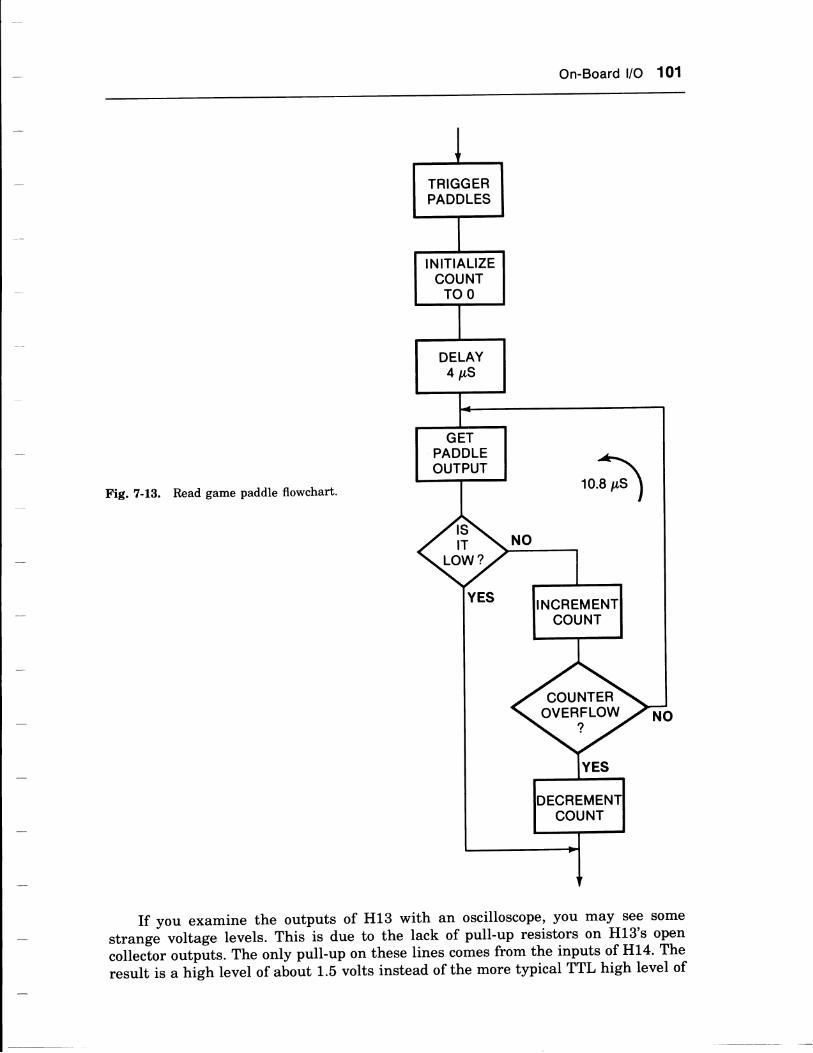
On-Board l/O 101
TRIGGERPADDLES
INITIALIZECOUNT
TO0
rraGET
PADDLEOUTPUT
INCREMENTCOUNT
COUNTEROVERFLOW
ECREMENCOUNT
Fig. 7-13. Read game paddle flowchart.
If you examine the outputs of H13 with an oscilloscope' you may see some
strange voltage levels. This is due to the lack of pull-up resistors on H13's open
collecltor outpits. The only pull-up on these lines comes from the inputs of H14. The
result is a high level of ulolt 1.5 volts instead of the more typical TTL high level of

102 Apple ll Circuit Description
Table 7-5. Soft Switches
Pin Signal State* Location Function
F14-4 TEXT MODEoff $c050 Graphics or mixed
On $cost All-Text* *
F14-5 MIX MODEoff $c052 All-Text or graphics
On $c053 Mixed
F14-6 PAGE 2off $c054 Select page 1
On $c055 Select page 2
F14-7 HIRES MODEoff $c056 Select LORES
On $c057 Select HIRES
F14-g ANOoff $c058On $c0se
F14-10 AN1 off $cosnOn $cosa
F14-1 1 AN2off $c05cOn $coso
F14-12 AN3 off $coseOn $cosr
*Off -0-LOw,On-1-High**When All-Text is selected, F14-5 and F14-7 are don't cares.
l.-ABour 2ms'*lTRIGGER
lcI
(F 13-7) | A
PDL (O) TIMERo"r:^l__
PDL (1) TrMEROUTPUT
>10 PRINT PDL (0), PDL (1)
>20 GOTO 10
Fig. 7-14. When two paddles are read *THT:"|; I*l:*
inserting delay, the second paddle value
3.5 volts. You may also find that the 1.5 volt high level varies as a function of theother inputs of H14. A l.ow level out of H13 looks normal however (0 to 0.4 volt).
Soft SwitchesThe eight soft switches appear at the outputs of addressable latch F14 (Fig. C-12*).Whenever the range $C050-$C05F is accessed, F13-10 goes low during @2. Thisenables F14. The three address bits ADL, ADz, and AD3 select one of the eightoutputs of F14. When enabled, F14 latches the data on pin 13 into the selectedoutput. Input F14-13 connects to address bit AD0, so even addresses will latch a 0into the output. Likewise, odd addresses will latch a 1 into the selected output.
T-

On-Board l/O 103
Table 7-6. On'Board l/O Locations
Locatlon Function Remarks
$c000$c010$c020$c030$c040$c050-$c05F$c060 & $c068$co0t & $c06e$cooe & $c06A$c063 & $c068$co0+ & $c06c$c065 & $c000$c066 & $co0e$c067 & $coor$c070
Keyboard Data lnputClear Keyboard StrobeToggle Cassette OutputToggle SpeakerGame Utility StrobeSoft SwitchesCassette lnputGame SWOGame SW1
Game SW2Game PDLOGame PDL1Game PDL2Game PDL3Game Paddle Trigger
{.
rl.
tlc
:N(
:N<
See Table 7-5
*Any of 16 locations starting with the listed location will perform the same function.
TWo output states times eight different outputs is equal to 16. Thus, all 16 loca-
tions in the range $C050-$C05F are separately decoded by F14. Table 7-5 shows
each location and its function. For example, to select a mixed TEXT and LORESdisplay from page 1, you would access locations $C050, $C053, $C054, and $C056.Use of the soft switches to control the display witl be covered in detail in Chapter 8.
SUMMARY
Tbble ?-6 is a summary of the VO address locations covered in this chapter.In the next chapter, we will explore the video display modes of TEXT, LORES,
HIRES, and mixed.
f

CHAPTER
The Video Display
The Apple II's video display is one of its greatest assets. There are three basic modes:black and white text, 16-color low resolution graphics (LORES), and 6-color highresolution graphics (HIRES). T\r'o additional modes allow text to be mixed witheither LORES or HIRES graphics. All three basic modes can display either a pri-mary page of memory (Page 1) or a secondary page of memory (Page 2). This chapterdescribes the video display circuitry and explains how colors are generated by thedigital electronics.
ovERvtEwWe start our overview of this chapter with a review of Apple's video display char-acteristics. In text mode, the display is 40 characters wide by 24 characters high.Each of these 960 characters is stored as one byte in a L024 byte block of memory.The range of this block is shown as follows:
Page 1
Page 2
The page to be displayed is selected bysoft switch address locations.)
In LORES mode, the display contains L92O pixels arranged 40 wide by 48 high.A pixel is a picture element, and is used here to describe one of the LORES colorblocks. LORES uses the same Page 1 and Page 2 memory ranges as text mode. InLORES, each byte stores two vertically adjacent pixels. Of a byte, the four low orderbits store the upper pixel, and the four high order bits store the lower pixel. Theinformation stored in the four bits is the pixel's color. There are 16 colors possible.
In HIRES mode, the display is 192 pixels high. A HIRES pixel is a mere dot,much smaller than a LORES pixel. It is a little difficult to specifr the number ofHIRES pixels in the horizontal direction. The width of a pixel is such that 280 pixelscan fit on one horizontal line. Thus, the HIRES horizontal resolution is usuallydefined as 280 pixels. However, there are actually 560 positinns where pixels can beplaced. Here is how we explain this concept. Divide the line into 280 equal parts
$4oo- $7FF$800- $BFF
the PAGE 2 soft switch. (Table 7 -5 lists the
r--
104

The Video Display 105
called cells. The design of the Apple is such that you can position a pixel to be
coincident with a cell You can also position a pixel so that it overlaps two cells,
one-half in one and one-half in another. Thken over the full width of the line, there
are then 560 positions where you can locate a pixel.We have not yet said anything about the color of the pixel. On a black and white
monitor, there is no color and each pixel is either on (white) or off ftlack). In black
and white HIRES we have 560 horizontal plotting positions.
Col.or HIRES is a different matter. Here the pixel's exact position will determine
its color. If we step a single pixel across the screen, stopping at each of the 560
locations, the pixel;s color will sequence through violet, blue, green' orange' violet,
etc. Any one color can appear a[ only one out of four positions. Thus, the color
HIRES horizontal resolution could be defined as 140 pixels'There are two more limitations on color HIRES resolution. First, two adjacent
pixels will not display in color, but will be a white dot. Of course you may want aittit" dot. Secona, tnl pixels stored by any one byte must be selected from one and
only one of the following two lists:
List 1 List 2
Violet BlueGreen OrangeWhite WhiteBlack Black
Thus, for example, you cannot mix green and orange pixels in the same byte.One memory byte stores the pixels for seven adjacent cells. The 280 cells per
line result in 40 bytes per line, and the 192 lines per screen result in 7680 bytes per
screen. In practice, an even 8K-byte memory block stores one HIRES screen:
Page 1
Page 2$2ooo- $3FFF$4ooo- $5FFF
Ther6 are two varieties of mixed mode: text mixed with LORES graphics andtext mixed with HIRES graphics. In both cases, the lower one-sixth of the screen
contains four lines of text characters.Fig. 8-1 is a high level block diagram of the video display process. When you
display text or graphics, you first configure the circuitry for the desired mode bysetting the soft switches under 6502 software control. Next you again use the 6502
to write to the desired locations in the screen memory. Meanwhile the video addressgenerator is always running, using the system clock to create the video address,
blanking, sync, and color burst signals. The video address maps to a memory ad-
dress, and then accesses the screen memory (RAM). The RAM's data is latched andmade available to the video generator. The video generator is enabled and disabledby the blanking signal. The video generator also uses inputs from the soft switchesto configure itself for the selected mode. Its function is to convert the latched datainto a video output. This video output is combined with the sync and color burstsignals in QB (Fig. 8-1). The output of Q3 is the Apple's composite video outputwLich is used to drive a monitor or an rf modulator. The video generator is thesubject ofthis chapter; the other blocks in Fig. 8-1 have been covered in preceding
chapters as noted in the figure.Fig. 8-2 is a block diagram of the video generator. The ICs that make up each
r

106 Apple ll Circuit Description
6502MICROPROCESSOR
PAGE 2
LATCHED DATASCREENMEMORY
(RAM)
VIDEOGENERATOR
(CHAP. 5)
(CHAP. 3 & 4)
BLANKING
MAPPER
VIDEOADDRESS
GENERATORCOLOR BURST
(CHAP. 6)
CLOCKFig. 8-1. Block diagram of video display process.
(CHAP. 7)
TEXT MODEMIX MODE
HIRES MODE
(CHAP. 5)
MEMORYADDRESS
VIDEO DATA
VIDEOADDRESS
+5 V
(CHAP. 4)
COMPOSITEVIDEO
OUTPUT
block are noted in the figure. The text generator consists ofa character generator, ashift register, a timer (for flashing characters), and gates to produce flashing andinverse text. The text generator is always running. It processes the latched data atits input into text at its output. The text video becomes an input to data selector Ag.
Shift registers 84 and 89 are configured by data selector A8. When HIRESMODE is low, each shift register takes four bits of latched data at its input andproduces a LORES pixel at its output. The LORES video becomes another input todata selector A9.
When HIRES MODE is high, A8 configures 84 and 89 into one long shift regis-ter. This long shift register takes the latched data at its input and produces sevenHIRES pixels at its output. The HIRES video becomes a third input to A9. Note thatshift registers 84 and 89 are always running, producing either LORES or HIRESvideo.
The TEXT MODE, MIX MODE, and HIRES MODE soft switches cause data

The Video Display 1OT
DL0-7 A3,A5,83
TEXT GENERATOR:
CHARACTERGENERATOR
SHIFT REGISTER
TIMER
INVERSE GATES
,^nt ,1trD
84,89
TEXTVIDE( )
A9
\-r\,/t-vl I
SYNC BURST
SH IFTREGISTER
LORES VIDEODATA
SELECTOR
+5 V
VIDEO DATA C Q3
HIRES VIDEO
SH IFTREGISTERCONFIGU-RATION
A8
L coMPo
Rl 1illh'TEXT MODEMIX MODE
HIRES MODEHIRES
TO
HIRES MODE
S-
I HRES
]*TPAGE,)
PAGE 2
Fig. &2. Block diagram of video generator.
selector A9 to select either text video, LORES video, or HIRES video to outputtoward Q3. There, the video is mixed with SYNC and COLOR BURST to create thecomposite video output.
TEXT MODE, MIX MODE, and HIRES MODE are combined to generate thesignal HIRES. HIRES and PAGE 2 map to memory as described in Chapter 5 and assummarized in Table 8-1.
The way in which data selectors A8 and A9 reconfigure the circuit under controlof the soft switches is a key concept in understanding the video generator. Eachconfiguration will be covered separately in the sections that follow.

108 Apple ll Circuit Description
Table 8-1 . Summary of HIRES and Page 2 Map to MemoryPAGE 2 HIRES Memory Space
001
1
01
01
Page 1 Text/LORESPage 1 HIRESPage 2 Text/LORESPage 2 HIRES
Text
The following soft switch settings configure the video generator for All-Tbxt:
TEXT MODE _ 1
MIX MODE _ XPAGE2 :0or1
HIRES MODE _ X(X : Don't care)
Fig. 8-3 shows the block diagram for this configuration. The first block, A5, is a2K by 8-bit ROM that has been programmed to contain the same ASCII characterset as contained in a type 2513 character generator. Thus A5 takes the six low orderlatched data bits and interprets them as a set of 64 characters. This character setincludes numerals, uppercase letters, and most ASCII symbols. It does not includelowercase letters and some remaining ASCII symbols. The output of A5 is a 5 by 7
dot matrix character (FiS. 8- ).The ROM, A5, generates the character one row at a time. Each row in the char-
acter is displayed by adjacent horizontal scan lines on the crt. It takes eight scanlines to display a complete character (including a vertical space above each char-acter). Of course these 8 scan lines also display the other 39 characters in a line oftext. As the crt beam scans down the screen, the signals VA, VB, and VC incrementat each line. This is shown in Fig. 8-4. Signals VA, VB, and VC address the appro-priate contents of A5 on each new row.
At any particular row, the dots on that row are output in parallel by A5. Shiftregister A3 (Fig. 8-3) converts the dots from parallel to serial. This means that itshifts out the dots one at a time as the crt beam scans across the screen. For eachcharacter, shift register A3 shifts seven times. It first shifts out a 0 (low), then thefive dots that make the character, then finally another 0. The two 0s are stored in A5and are used to create the horizontal space between characters. This is seen in Fig.8-4. The figure also shows the video waveform that is generated for the third row ofthe character "A."
Referling again to Fig. 8-3, flashing timer 83 provides the rate for flashingcharacters and the cursor. Gates 811-11 and 813-4 decode the high order two bits(DL6 and DL7) of each character to determine its display mode (see Table 8-2).
DL7 DL6 Mode001
1
01
01
lnverseFlash ingNormalNormal
|---
Table 8-2. DLO and DLZ Determine Display Mode

The Video Display 109
a-it
(,z=zJdl
TEIUF9,(5llJcr
sfI
ADFo
t\
FF
IFFo
cr.LU-L6 z-I;ofiry8.fr
(57r.-r IIJ-a>jtrlL
--LUTAaE19tL7
rICrUJOFFo<>{rE(^)crUJ;7<z*IUJoo
od<
Fig. 8-3. Block diagram of text mode.

110 Apple ll Circuit Description
VC VB VA
0
1
0
1
0
1
0
1
0
0
1
1
0
0
1
1
0
0
0
0
1
1
1
1
7x 8 CELL
5x7 CHARACTER
VIDEOWAVEFORM
DLO THROUGH DLsSELECT ONE OF 64CHARACTERS.
Fig. 8-4. Text character format.
KEY, f] vtDEo Low, BLAcK
I vrDEo HrcH, wHrrE
Note that flashing characters are merely alternating quickly between normal andinverse.
The output of 813-4 contains the flash/inverse information for the current char-acter. This information is stored in register A10, and is then presented to one inputof exclusive on gate B2-Ll. The exclusive on gate inverts the serial data from theshift register under control of the flash/inverse signal. Fig. 8-5 shows the letter "A"as it would appear in inverse video. Note that the entire 7 by 8 cell is inverted, notjust the 5 by 7 character. The video waveform for the third row in the cell is alsoshown in Fig. 8-5. The waveform is simply the inverse of the waveform fromFig. 8-4.
Returning to Fig. 8-3, the text video signal from 82-11 next passes through dataselector A9. At A9, the video signal can be turned off by the blanking signal stored
VIDEOWAVEFORM
KEY' fJ BLAcKX 7 CHARACTER
F
WHITE
Fig. 8-5. Inverse text character.

The Video Display 111
in register A10. By this, we mean that during the blanking interval, the video signalis forced to 0 (low) to create a black portion of the screen. After A9, the video nextpasses through flip-flop 810-5 and then to Q3. At Q3, the video is mixed with SYNC
and COLOR BURST to create the composite video output. (Blanking and the Q3mixing process were described in Chapter 4.) This completes the path of the textcharacters through the video generator.
HIRES
The following soft switch settings configure the video generator for HIRES:
TEXT MODE _ O
MIX MODE _ O
PAGE2 :0or1HIRES MODE _ 1
Fig. 8-6 is the block diagram for HIRES mode. Data selector A8 configures 4-bit shift
""girt""r 84 and 89 into one long 8-bit shift register. Each byte to be displayed is
toaaed into the parallel input of this shift register. The contents are then shifted outone HIRES pixel at a time as the crt beam sweeps across the screen. If the bytecontains green or violet pixels, the high order bit (DL7) will be 0, and data selectorA9 will select the output of the shift register. If the byte contains blue or orangepixels, DL7 will be 1, and data selector A9 will select the output of flip-flop A11-9.
The output of A11-9 is the shift register's output delayed by one 14M clock.The output of data selector A9 passes through flip-flop 810-5 on its way to Q3.
At Q3, it is mixed with SYNC and COLOR BURST to create the composite video
output. Just as was the case in text mode, a blanking signal is applied to A9 to force
the video to black during the blapking interval-Dl7 and BLANKING are stored inregister A10 on their way to A9. The key elements of Fig. 8-6 are the shift register
84,89 A9
+5VGREEN, VIOLET
810-5DLO-DL7
ORANGE,
COMPOS-ITEVIDEOOUTPUT
A1 0
DL7 BLANKING
Fig. 8-6. Block diagram of HIRES generator.
IUEBL
DATASELECTOR
--
8 BITSHIFT
REGISTER
SERIALOUTPUT
PARALLELINPUT
DATASELECTOR
REGISTER
r-

112 Apple ll Circuit Description
and the ability of A9 to select the shift register's output either directly or delayed byA11-9. This selection is under control of DL7.
Now that we have the circuit arrangement in mind, let's see how it actuallyproduces colors. Recall from color television theory that a video signal with a com-ponent at 3.58 MHz (the color burst frequency) will produce a color on the screen.The hue or tint of that color will be a function of the signal's phase relative to thephase of the color burst signal. (If you are not familiar with color video techniques,you should review Appendix A at this time.) Fig. 8-7 shows color hue as a function ofphase angle relative to color burst.
ORA
RED
\NGE 90"
135"xoLl45"
BURST00
315",/
190'
225"
270"
ET
YELLOW
BLUE
GREEN
Fig. 8-7. Color hue as a function of phase angle relative to burst.
Let's take the case of one byte of violet in the upper left corner of the HIRESscreen. We can do this with a "POKE 8L92,85" from BASIC. When the video scan is atthe upper left of the screen, the decimal value 85 will load into shift register B4lBg asshown in Fig. 8-8. Note that this value is an alternating pattern of 1s and 0s. The LSB(DL0) is immediately available (point A). The shift register then shifts six times,creating the video waveform shown, as the bits DLO through DL6 shift out.
Above the video waveform we have shown COLOR BURST at the same timescale. Observe that the video waveform has the same frequency as COLOR BURST,but the video is delayed by 135 degrees. The color wheel (Fig. 8-Z) shows us that aphase delay of 135 degrees from burst creates the color violet.
Fig. 8-9 shows how green is generated. This time we POKE 42 into location8L92. When the pattern shifts out of the shift register, we get the video waveformshown. Again it has the same frequency as COLOR BURST, but is delayed 315degrees. This corresponds to the color green in Fig. 8-7.
Fig. 8-10 depicts the display method for blue. Here we POKE the value 213 intolocation 8192. The low order seven bits are the same as they were for violet. Thus,we get the same waveform at the shift register's output. The MSB (DL7) is 1, how-ever, so data selector Ag selects the output of flip-flop A11-9. The flip-flop delays theshift register output by one 14M clock period. This is equivalent to 90 degrees at3.58 MHz as shown in Fig. 8-10. The net result is to delay the video waveform 225degrees relative to burst. This corresponds to the color blue in Fig. 8-2.
r

The Video Display 113
DLO
DL1
DL2
DL3
DL4
DL5
DL6
DL7
] PoKE 8192,Bs
DLO
DL1
DL2
DL3
DL4
DL5
DL6
DL7
SHIFTDIRECTION
COLORBURST
COLORBURST
SHIFTDIRECTION
\ 135" DELAY1\ 1 1 1
000
BURST
Fig. 8-8. HIRES violet.
BURST
]poKE 8192,42
GREEN
Fig. 8-9. HIRES green.
Finally, in Fig. 8-11, we show how orange is produced. We poke the value 170
into location 8192, and this generates the "green" waveform at the shift register'soutput. The MSB (DL7) is 1, so A9 selects the output from 411-9. ,{11-9 delays the
"gl6en" waveform by one L4M clock. The net result is a video waveform delayed 45
degrees from burst. This corresponds to the color orange in Fig. 8-7.
There now remain the two "colors" black and white. For black we simply store 0
84,89
VIOLET
B,4,89
r

114 Apple ll Circuit Description
84,89
?rrens*|
DLO
DL1
DL2
DL3
DL4
DL5
DL6
DL7
] poKE 8192,213
DLO
DL1
DL2
DL3
DL4
DL5
DL6
DL7
] poKE 8192,1T0
14M
SH IFTDIRECTION
COLORBURST
A1 1-9 \225O DELAY90'
DELA
BURST
Fig. 8-10. HIRES blue.
COLORBURST
ORANGE
BURST
B,4,89
14M
SHIFTDIRECTION
DELAY
Fig. 8-11. HIRES orange.

The Video Display 1 15
or 128 in memory (Fig. 8-12). The seven 0s will shift out creating a continuous lowsignal. This corresponds to black. For white, we store L27 or 255 (Fig. 8-13). Theseven 1s will shift out creating a continuous high signal. This signal has no compo-nent at 3.58 MHz, so there is no color. A high level corresponds to white, so that iswhat we get.
+5 VDLO
DL1
DL2
DL3
DL4
DL5
DL6
DL7
] poKE 81 92,121OR
] poKE 81 92,2ss
Fig. 8-r3. HIRES white.
Before leaving our overview of the HIRES display, we must introduce the topicof even and odd bytes. The previous examples showing the six HIRES colors all usedan even byte, location 8192. Fig. 8-14 shows what happens when we consider botheven and odd bytes. At the top of the figure we have shown color burst. The secondwaveform is the video output for a violet line. It starts out just like the example inFig. 8-8. The value 85 produces the alternating pattern 1010101.
The next segment of the line is stored in an odd location. If the line is to con-tinue with the same color (same phase relative to burst), the odd segrnent must havethe pattern 0101010. This is the value 42, thLe complement of 85. The same color isstored as two different ualues, depending on whether the byte is euen or odd. This canbe explained by noting that the time used to display one byte contains three andone-half cycles of 3.58 MHz. Thus, the relative phase of COLOR BURST changes by180 degrees every byte. HIRES plotting routines take this into account.
84,89
B,4,89
OV
] poKE 81 92,0OR
]poKE 81 92,128
Fig. 8-L2. HIRES black.
COLORBURST
+5 VOV
F zrsnsl
DLO
DL1
DL2
DL3
DL4
DL5
DL6
DL7

116 Apple ll Circuit Description
COLOR BURST
VIDEO \35'DELAY
We haveremain more
LORES
The following
000or10
I+EVEN BYTE (vlOLET=85)--+ODD BYTE (VIOLET =a2llFig. E-14. Even and odd HIRES bytes.
now explained in concept how the HIRES colors are produced. Theredetails that will have to wait until later in this chapter.
soft switch settings configure the video generator for LORES.
TEXT MODEMIX MODE
PAGE 2HIRES MODE
Fig. 8-15 shows the circuit configuration for this mode. Data selector A8 arrangesshift registers 84 and 89 into two separate 4-bit shift registers. In LORES mode,each byte stores two pixels. Bits DL0-3 store the upper pixel; these bits parallel loadinto 84. Bits DL4-7 store the lower pixel and these bits parallel load into Bg.
While the pixels are being displayed, the bits rotate in the shift registers in amanner similar to that of HIRES. In LORES, however, each shift register provides
B4 A9EVEN +5V
DLO-DL3
810-5
DL4-DL7 COMPOS-
ITEVIDEOOUTPUT
A10
\Z*uppER ptxEL (vc = o)
Nh LowER PIxEL (vc = 1)
tEACH BYTE IN SCREEN MEMORYSTORES TWO LORES PIXELS
HO VC BLANKING
4 BITSH IFT
REGISTER
(UPPERPrxEL) DATA
SELECTOR4-BITSH IFT
REGISTER
(LOWERPrxEL)
DATASELECTOR tll
REGISTERllllll
Fig. 8-15. Block diagram of LORES generator.

The Video Display 117
both an even and an odd output. Data selector A9 selects between even and oddoutputs under control of signal H0. Signal H0 alternates between 0 and 1 as the crtbeam scans over alternating even and odd bytes. You can refer to Fig. 3-4* to see thetiming of H0. The purpose of this even/odd circuit configuration will be explainedshortly.
Data selector A9 also selects between the upper and lower pixels under controlof signal VC. Here you should refer to Fig. 4-1* to see the timing of VC. Signal VCalternates between 0 and 1 every four scan lines. The height of a LORES pixel isalso four scan lines. When VC:0, A9 selects the upper pixel. When VC:1, A9selects the lower pixel. This is depicted in Fig. 8-16 where we have shown signalsVC and H0 coordinated with four LORES pixels.
PPER ODD PIXEL
8 SCANLINES
rt
Fig. 8-16. LORES pixels.
The blanking signal at data selector A9 forces the video to black during theblanking interval. Signals H0, VC, and BLANKING are stored in register A10 be-
fore they go to A9. The video out of A9 passes through flip-flop B10-5 on its way to
Q3. At Q3, the video is mixed with SYNC and COLOR BURST to create the compos-
ite video output.Let's briefly review the LORES block diagram. The key elements are: (1) the
shift registers with separate odd and even outputs, and (2) data selector A9 whichselects upper and lower, even and odd inputs under control of VC and H0.
We now move from the block diagram to an explanation of LORES color gener-
ation. Each pixel is stored as four bits in memory. The pixel color is coded by these
four bits as listed in Thble 8-3. The table lists the color names used in Apple's docu-
mentation and alternative color names used in this book. The alternative names willaid our discussion, and you may assume that hereafter any LORES color mentionedin this book will use the alternative name.
In Table 8-4 the 16 colors are divided into four groups. We will examine one
color from each of the first three groups and three colors from the miscellaneousgroup.
U
/

118 Apple ll Circuit Description
Table 8-3. LORES Colors
Table 8-4. LORES GroupsMediumGroup
LightGroup
DarkGroup
MiscellaneousGroup
9 Orange3 Violet6 Blue12 Green
13 Light Orange11 Light Red7 Light Blue
14 Light Green
8 Dark Orange1 Dark Red2 Dark Blue4 Dark Green
0 Black5 Gray 1
10 Gray 215 White
Fig. 8-17 shows the generation of LORES blue. We start by poking a 6 intomemory location L024 (the upper left pixel on the screen). When the video addressscans this pixel, the low order four bits load into shift register B,4. Bit DLO (a 0) isimmediately available at the video output, point A. The shift register now shifts 13times. On each shift, the serial output is loaded into the other end of the register.Thus, the same four bits recirculate through the shift register, generating thewaveform shown.
COLOR BURST is drawn above the video waveform at the same time scale.Both signals have the same frequency, 3.58 MHz. We have drawn tic marks at thecenter of the positive portion of each signal so that we can measure their relativephase. As shown, the video signal is delayed 225 degrees relative to COLOR BURST.From Fig. 8-7 we see that 225 degrees corresponds to blue. You may also wish tonote that the video signal for LORES blue is the same as that for HIRES blue,Fig. 8-10.
Fig. 8-18 shows the generation of LORES light blte. This time we POKE a 7into location 1024. Again, when the upper left pixel is scanned, four bits load intothe shift register then rotate to create a video waveform at the serial output. Thiswaveform has the same frequency as burst and is delayed 180 degrees. From Fig. 8-7we see that 180 degrees also corresponds to blue.
Bit Positions Golor Names
UpperPixel:LowerPixel:
0
4
1
5
2
6
3
7Decimal
Fro m Apple llReference Manual
AlternativeNames
0000000100100011010001010110011110001001101010111100110111101111
01
234567I9
1011
12131415
BlackMagentaDark BluePu rpleDark GreenGray 1
Medium BlueLight BlueBrownOrangeGray 2PinkLight GreenYellowAq uamarineWhite
BlackDark RedDark BlueVioletDark GreenGray 1
BlueLight BlueDark OrangeOrangeGray 2Light RedG reenLight OrangeLight GreenWhite

The Video Display 119
BURS'
\ 22''DELAY84 cE.,rAr ntr \,sERrAL otl
-t I o 1 10 o 1 1 o o 1 10 o 1
Ileoxe1024,6 50o/o
DUTY CYCLE
BURST
Fig. &17. LORES blue.
The color waveform in Fig. 8-18 differs from those presented up to now; it doesnot have a 50Vo duty cycle. This waveform is high for three out of four counts, so ithas a duty cycle of 75Vo. Stated another way, its average value is 75Vo of the wayfrom black (low video level) to white (high video level). This means the color displayof this signal will be brighter than the display of the 50Vo duty cycle signal of Fig.8-17. Thus, Fig. 8-17 shows "medium" blue and Fig. 8-18 shows "light" blue.
279 nS
BURST
75o/o
I o,-o
I ot''1 DL2
Io,-t
DLO
DL1
DL2
DL3
] eore 1024,7
a(- DUTY CYCLE
11101110111011
BURST
SERIAL
Fig. 8-18. LORES light blue.
BLUE

120 Apple ll Circuit Description
Let's move to Fig. 8-19 which shows dark blue. This time we POKE a 2 intolocation 1024. The bits rotate and generate the waveform shown. This signal is de-
fayed 180 degrees from burst, again blue. Note that this signal has a 25Vo duty cycle.Its average level is closer to black than to white. Thus, we get "dark" blue.
BURST/zts ns.
DLO
DL1
DL2
DL3
010 0010 0010001
] eoxe 1024,2
BURST BLUE
Fig. 8-19. LORES dark blue.
The other colors in the first three groups of Table 8-4 can be explained in amanner similar to the blue colors. The dark colors have duty cycles of 25Vo, themedium colors have duty cycles of 50Vo, and the light colors have duty cycles of 75Vo.The phase angles of the other hues will, of course, be different.
The black, white, and gray "colors" in the miscellaneous group contain no colorsince they do not contain a 3.58 MHz component. Black (all 0s) is a continuouslow-a dc signal. White (all ls) is a continuous high; another dc signal. A dc signalhas no 3.58 MHz component, so we get no color, just black or white.
Gray is a little more interesting, and in Fig. 8-20 we show the generation ofLORES gray 1. The value 5 is poked into location L024. This is an alternating pat-tern, and when the bits rotate they produce the \Wo daty cycle shown. This signalhas a frequency twice that of COLOR BURST or 7.16 MHz. It is a square wave, andthere will be harmonics above 7.16 MHz. However, there will be no componentsbelow 7.16 MHz. Specifically, there is no 3.58 MHz component. Without thiJcompo-nent, there is no color. Since the duty cycle is 50Vo, the average level is half waybetween black and white-this is gray. Gray 2 is similar to gray 1; the two patternsare complements.
We have now shown in concept how six of the LORES colors are produced. These6 are typical of the full set of 16 colors. The video waveforms and phase angLee of allthe LORES colors are summadzed in Fig. 8-21.
Recall that in HIRES mode, data for the same color was stored as differentvalues in even and odd bytes. You may also recall that we promised to explain theseparate even and odd shift register outputs in the LORES block diagram, Fig. 8-15.
B4
r

The Video Display 121
BURST
I o,-o
I ot''
l::IPoKE
1024,5
B4
750Y"
DUTY CYCLE
Fig. 8-20. LORES gray 1.
The Apple's method for handling the everVodd problem in LORES differs from themethod used in HIRES. In HIRES, it is left to the software to sort out even and oddbytes. In LORES, the problem is solved in hardware. Fig. 8-22 shows the scheme,using blue as an example. First, data from an even byte is loaded into shift register84. The data is decimal 6 which has the binary pattern 0110. The pattern rotatesand generates the video waveform shown, starting at point A and ending at point B.This is the same waveform that was shown for the even byte blue of Fig. 8-17.
The next adjacent pixel is stored in an odd byte. Its display starts at point C. To
continue the video signal at the same phase angle, the pattern starting at point C
must be 1001. Here is how it works. We store the same decimal value (6) in the oddbyte. When the pixel is scanned, the 6 loads into 84. Since this is an odd byte, sigiralH0 causes data selector A9 to select the "odd" tap of shift register 84. When 84 isloaded, the 1 at the odd tap is immediately available at the video signal, point C.The bits then rotate from this starting point, giving us a 1001 pattern.
In summary, A9 selects even and odd outputs of 84, allowing one data value torepresent the same LORES color for both even and odd bytes. Since this is handledin the hardware, the programmer need not worry about it.
Our overview of LORES graphics has used shift register 84 as an example. Theoperation of shift register B9 is the same as that of 84. 89, however, operates on thehigh order four bits of data, and displays the lower pixel.
Mixed HIRES and Text
The following soft switch settings configure the video generator for mixed HIRESand text:
TEXT MODE :0MIX MODE _1
PAGE 2 :0 or 1
HIRES MODE _ 1
Note that both the text and HIRES will come from the same page (determined by thePAGE 2 soft switch). Fig. 8-23 shows the block diagram for this configuration. Boththe text generator and the 8-bit shift register operate on the latched data as previ-ously described. While the crt scan is in the top portion of the screen, data selectorA9 selects the HIRES from the 8-bit shift register. When the scan gets five-sixths of
f

122 Apple ll Circuit Description
tllttttPHASEcoLoR -r r-r r-r r-r ANGLE:;uili oo.
COLORVALUE:
0
1
7
8
I
10
11
12
13
COLORNAME:
BLACK
2
3
4
5
6
225'
180'
GOOO
00
450
14
15
LIGHr *to o *'
MEDIUM GREEN o t'u'
LrcHr oRANGE O o"
LrcHr .REEN e rro.
DARK rro O o.
DARK BLUE O T*'
vroLEr Ol3s'DARK GREEN O TTo'
GRAY 1
MEDIUM BLUE
LIGHT BLUE
DARK ORANGE
MEDIUM ORANGE
GRAY 2
WHITE
-l
Fig. 8-21. LORES colors.

The Video Display 123
BURSTCOLOR
VIDEO(BLUE)
A
225" DELAY
01 10 01 10 01<- EVEN BYTE (PATTERN
BC10 0110 0
-0110)+>{*-ODD11001100110BYTE (PATTERN - 1oo1)-+
A9
VIDEOI POKE 1024,6
HO
Fig. 8-22. Even and odd LORES bytes.
V 4 both go high. This causesbottom one-sixth of the screen
the way down the screen, video address lines V2 andA9 to select the text generator output. As a result, thecontains four lines of text.
Mixed LORES and Text
The following soft switch settings configure the video generator for mixed LORESand text:
TEXT MODEMIX MODE
PAGE 2HIRES MODE
or1
Both the text and LORES will come from the same page. Fig. 8-24 shows the blockdiagram for this configuration. Both the text generator and the two shift registersoperate on the latched data. While the crt scan is in the top portion of the screen,data selector A9 selects LORES pixels from the shift registers. When the scan getsfive-sixths of the way down the screen, video address lines V2 and V4 both go high.This causes A9 to select the text generator output. As a result, the bottom one-sixthof the screen contains four lines of text.
This concludes the overview of the Apple II video display. The block diagramsand signal waveforms in this section were drawn to illustrate only the concepts. As aresult, some of the drawings may not correspond exactly to the actual circuit im-plementation or to waveforms actually observed on an oscilloscope. These detailswill be provided in the circuit analysis that follows.
hlr1 DL2
Ior-s
-0-1-0-0

124 Apple ll Circuit Description
A3,A5,83
TEXTGEN ERATOR
84,Bg
H IRES
\DATA --.
SELECTOR /,'///a/
8 BITSHIFT
REGISTER
DLO-DL7
VIDEO
Fig. E-23. Block diagram of mixed HIRES and text.
DETAILED CIRCUIT ANALYSIS
Text ModeOur detailed analysis of text mode starts with character generator A5 and shiftregister AB (Fie. C-16*). We then follow the signal through data selector A9 andflip-flop 810-5.
Character Generator-Ic A5 is a type 23168 ROM that stores all the row andcolumn dots for a set of 64 dot matrix characters. Inputs AB through A8 are thecharacter address. They receive latched data bits DLO through DL5. These are thesix bits of each byte in text memory of the Apple that store the character. Inputs A0,A1, and A2 of IC A5 are the row address. They receive the video address lines VA,VB, and VC. As the crt beam moves down the screen, these address lines select oneof the eight rows that make up each character.
Input A9 of IC A5 connects to DL6. Character generator A5 is programmed so
I---

The Video Display 125
TEXTGENERATOR
UPPERPIXEL
\ \ \ \ \ \-t \-t,
-?,-/ttt //
a///
^r-FaDATASELECTOR
4 BITSH IFT
REGISTER
4 BITSH IFT
REGISTER
DLO-DL7
A3,A5,83
TEXT
VIDEO
LOWERPIXEL
812-6v2
v4
Fig. 8-24. Block diagram of mixed LORES and text.
that output 08 exactly follows address input A9. The effective result is to connectDLG to 811-12.
Input A10 of IC A5 connects to DL7. A5 is programmed such that input A10 is adon't care.
As we have just described, the connection of DL6 and DL7 to A5 has no effectwith the ROM supplied by Apple Computer. The purpose of the connections is so
that you can provide your own ROM or EPROM containing additional characters.The additional characters would be accessed via DL6 and DL7. Additional flexibilityis provided by bow ties 9, 10, and 11. These may be cut and connections made to A5inputs A9 and A10 from external sources, such as the game UO or a simple switch.The external source could then select a character set via A5 inputs A9 and A10.Specific implementation of user character sets is not covered in this book.

126 Apple ll Circuit Description
The Apple supplied A5 ROM is programmed so that outputs 01 and O7 arealways low. This provides a blank dot on the left and right of each character. Theresult is the horizontal space between characters. In a user supplied ROM, theseblank dots may be programmed to form part of a character. An example would be agraphics symbol.
Shift register A3 takes the parallel output of A5 and shifts it out one bit (dot) ata time. The resulting serial bit stream passes through exclusive on gate B2-LL whereit can be inverted to create inverse video. The inversion is controlled by the twolatched data bits, DL6 and DL7. These two bits are decoded by gates 811-11 and813-4. The resulting signal is applied to input pin 6 of register A10 where it isstored. The signal exits A10 on pin 12. The inverse signal has to be stored in A10because DL6 and DL7 do not remain valid for the full character display time.
Normal and Inuerse Text-When DL7 is high, B13-4 and A10-12 will be low.The resulting low at B2-L2 allows the serial bit stream to pass noninverted. Thisgives us a character in normal video (white on black). Note that when DLZ is high,DL6 is a don't care. When DL6 and DL7 are both low, 813-4 and 410-12 will behigh. This high at B2-t2 inverts the serial bit stream, giving us a character in in-uerse video (black on white).
Flashing Tert-When DL7 is low and DL6 is high, the signal at 811-11, 813-4,and 410-12 will follow the output of timer 83. B2-11 now alternately inverts orpasses noninverted the serial bit stream. This gives us a flashing character at about2 Hz.
Text Mode Circuit Configuration-Before moving on to the detail timing, wemust explain how data selectors A8 and A9 configure the video generator for text.The TEXT MODE soft switch will be set, so 813-12 is high. Non gate 813-13 is low,and after three ffi pulses, this low propagates through flip-flops B5-2 and 88 tomake B8-2 low. Thus 811-6 (HIRES) is low, assuring that we will fetch charactersfrom the text page and not the HIRES page.
Non gate A12-10 is high, AI2-L} is low, and A11-6 is high. (A11-5 is used as aninverter.) This high at data selector A8 causes it to select its "1" inputs. Pin B5-2 islow, and this low passes through A8 to A8-7. The low is then stored in A10 on 14Mrising while LD194 is high. The low next appears at A9-10. Recall that 412-13 islow. This low appears at A9-9.
If you have been following this discussion carefully, you will notice that Ag isnow set up to select either input pin 3 or 4. These pins both connect to the video textfrom 82-11.
Shift Register A3 -As we ease into the details of text generation, let's explorethe clock and load inputs of shift register A3. These three inputs are driven fromsignals previously discussed and shown again at the top of Fig. 8-25A. Pins 6 and 7are connected internally to a NoR gate that provides the IC's internal clock. Thedevice is clocked on the falling edge as shown in the fourth line of Fig. 8-254. Oneach clock, the IC either shifts (if pin 15 is high) or loads parallel data (if pin lE islow). Signal LD-FE controls the mode (shift or load) of AB.
Text Mode Timing Diogrq-:llE 9-26* shows the display timing of two textcharacters. Signals 14M and ABEOC_K are shown at the top. The t*a" of A3 isshown next to each falling edge of Affi'eK (S : shift, L : load). (Remember thatAffiTR is an internal IC-signal and cannot be viewed on an oscilloscope.) Alsoshown in the figure are LD194, the video address, and the latched data-all previ-ously discussed.
The first character that we have shown is the left-most character on a line,
I-

The Video Display 127
*l F6e.8 ns
14M
7M
(A) Clock and loadwaveforms.
LDPS
A3 CLOCK
A3 MODE
L = LOADS - SHIFT
A3-6 (7M)
A3-7 (14M)A3 CLOCK(B) Clock input gate.
Fig. 8-26. Clock and load inputs-shiIt register A3.
character 0. The second is the right-most character on a line, character 39. The 0 isan even character and 39 is an odd character. Tb add even more variety, we havemade character 0 be in normal video and character 39 be in inverse video. We havedrawn the timing as if these were the only two characters on a line. This is so thetiming relationship between adjacent characters can be shown. There are, of course,really 40 characters per line.
Note that Fig. 8-26* shows one horizontal scan line or one row through thecharacters. The uppercase letters in the figure are references to the text (our normalpractice in this book). The lowercase letters represent the data values of thewaveform at various points. The seven signals A3-Qo through A3-Q" are shown asaids to understanding the timing. They are not available externally to IC A3.
Euen Character Timing-At point A, the video address for character 0 becomesvalid. Since we are at the left edge of the display, the video address is decoded toremove blanking at point B. After the video address maps to memory, the characterappears as latched data at point C. During the time that the video address and thelatched data are both valid (point D), VA, VB, VC, and DLO through DL5 all addresscharacter generator A5 (Fig. C-16). Character generator A5 responds with sevenhorizontal dots on its outputs 01 through O?. On ffiLOC-K falling (point E in Fig.8-26*), these seven bits load into shift register A3 (points F through M). The valuesof these seven bits are represented in Fig. 8-26* as b through h (corresponding totheir 74166 signal names).
Also while the latched data is valid, DLG and DL7 are decoded by 811-11 and813-4 to become the inverse signal. It is loaded into A3 at point N. It is also loadedinto register A10 on L4M rising pulse while LD194 is high, point O. The signal atA10-12 is low, so the output of A3 passes to B2-11 noninverted, point P. BLANKING(C14-6 in Fig. C-20*) is now low, so on 14M rising pulse while LD194 is high, A10-13goes low (point Q in Fig. 8-26*). This enables data selector A9 (Fig. C-16*) via its pin7. We already know that A9 is set to select input pin 3 or 4. Thus when enabled, A9sends the text to 810-2. This flip-flop is clocked every 14M rising pulse, so the text
F

128 Apple ll Circuit Description
appears at the video output at point R in Fig. 8-26*. This first dot is actually a darkdot to the left of the character, so 810-5 is low. Each dot is 140 nS wide.
The purpose of flip-flop 810-5 is to reclock the video data. This is so that anyglitches created by the preceding logic are eliminated. After the delay through810-5, the video data will also have the correct phase relative to COLOR BURST.This is important for the color graphics modes.
On the next AB CLOCK (point T), A3 is in shift mode and the eight bits storedin AB shift as shown in the figure. Bit b shifts into Qc, bit c shifts into Qo, etc. Theinverse signal at 410-12 shifts into A3-Qa, and bit g shifts into Qs. On the next 14Mrising, bit g appears at the video output (point U). This process continues for fourmore shifts, giving us bits f, e, d, and c at the video output. One more shift gives us adark dot to the right of the character, point V.
The connections at A3-1 and A3-2 do nothing. This is because A3 is alwaysloaded with new data before the "a" bit shifts out.
Odd Character Timing-While the even character is shifting out, the video ad-dress and latched data for the odd character become valid (point W). Again, A3 isloaded with five character dots with a dark (low) dot on each side. This character isin inverse, however, so a high from 813-4 loads into '4'10-12
(point X). This high atB2-L2 inverts the serial bit stream starting at point Y. This high appears at thevideo output starting at point Z. The high creates a lighted dot to the left of theinverse character. On the next five shifts of A3, the bits g through c appear invertedat the video output. One more shift creates a lighted dot to the right of the character,point AA.
Since this is the right-most character on the line (character 39), BLANKINGgoes high when the video address changes (point BB). On the next 14M rising pulsewhile LD194 is high, 410-13 goes high (point CC). This disables A9, and horizontalblanking starts after one more 14M clock pulse (point DD). This concludes our de-tailed analysis of text mode.
HIRES Mode
Our analysis of HIRES mode starts with the configuration of the video generator by
the soft switches. Then we follow in detail the timing of the signals through thecircuitry.
HIRES Mode Circuit Configuratinn-Fot HIRES graphics, the TEXT MODEand MIX MODE soft switches are low. This results in a high at 813-13 (Fig. C-16*).
After threeEs pulses, this high propagates through flip-flops B5-2 and B8- Thismakes 811-5 high. Since the HIRES MODE soft switch is high at 811-4, 811-6(HIRES) is high- This arranges the memory system to map video addresses to theHIRES page.
HIRES MODE high at A12-I2 results in a high at 411-6. (Recall that A11-5 is
used as an inverter.) This high at data selector A8 pin 1 causes it to select its "L"inputs. Thusfif at A8-10 passes through to A8-9 and pin 10 of shift register 84 and
Bg. pins 9 and 11 of 84 and 89 connect to LD194 and 14M. Pin 11 is the clock inputand pins 9 and 10 control the shift modes of 84 and 89 as shown in Thble 8-5.
Ba and 89 load on 14M rising whileEl and LDt94 are high. 84 and B9 shift left on14M rising pulse whileTilf is high and LDL94 is low. A left shift is a shift in thedirection of D3 toward D0. The clock edges on which the loads and shifts occur areshown in Fig. 8-27. This figure also shows the clock edges on which A10 loads.
Returning to A8, pin 1 is high, so data input on pin 3 is output on pin 4. Thus,

The Video Display 129
Table 8-5. S1 and S0 Control Shift Modes
S1(Pin 10)
s0(Pin e)
Mode
001
1
01
01
Do NothingShift RightShift LeftLoad
*l l--09.8 nS
14M
7M
1D194
410MODE
84/89MODE
L - LOADS = SHIFT
Fig. 8-27. Clock and shift inputs-ICs A10, 84, and 89.
bits that shift out of 89-15 shift into B4-7. This is how 84 and 89 become one long8-bit shift register.
The signal at B5-2 is high as previously described. This high at 4'8-6 passes toA8-7, is latched in A10, then appears at A9-10. The signal at A12-13 is low (again aspreviously described), and this low appears at A9-9. Signal DL7 at 48-13 passes toA8-I2, is latched in A10, then appears at A9-11. These three select inputs of A9(pins 9, 10, and 11) cause it to select either input pin 1 or pin 2 under control of DL7.When DL7 is low, A9-2 is selected. This comes from 84-15, the direct output of theshift register. When DL7 is high, A9-1 is selected. This comes from A11-9, the shiftregister's output delayed by one 14M clock cycle.
HI&ES Mode Timing Diagrarn-Fig. 8-28* shows the detail timing of HIRESdata. The timing for 14M, the video address, and the latched data have been derivedpreviously. The clock edges on which A10, 84, and 89 shift and load are also shown.This information has been duplicated from Fig. 8-27.
The two bytes shown are the left-most display byte (an even byte), and theright-most display byte (an odd byte). The waveforms represent one horizontal scanline. We have shown the timing as if only two bytes were displayed on a line. Inpractice, 40 bytes are displayed.
Euen Byte Timing-The video address for the even byte becomes valid at pointA. Since this is the left-most byte, BLANKING goes low at the same time (point B).The video address maps to the HIRES screen memory, and the memory returns thebyte to be displayed as latched data, point C. While the latched data is still valid, itis loaded into 84 and 89, points D through K. The numbers (0 through 7) shown inthe waveforms correspond to the bit's origin. For example, at point K, bit DLO loadsinto 84 and appears at 84-1"5.
L

130 Apple ll Circuit Description
At the same time that 84 and 89 are loaded, DL7 loads into A10-14 andBLANKING loads into 410-13 (point M). Data selector A9 is enabled by the low on410-13. Assume for now that DL7:0. This causes A9 to select input pin 2. Thus, bitDLO from 84-15 appears immediately at Ag-5, point N. On the next 14M risingpulse, bit DLO appears at 810-5, the video output (point P). The bit is 140 nS widewhen displayed.
On the next 14M rising pulse, B4 and 89 shift. This moves bit DLl to B4-15,point Q. The other seven bits also shift as shown by the arrows. Note that since89-15 connects to B9-7, DL4 shifts into Bg-12. This is indicated by the arrow to pointR. This arrangement serves no function in HIRES, nor does it do any harm.
The data shifts five more times during the display time of this byte. The latcheddata appears in the video output in the order DLO to DLG (point P to point T).
Odd Byte Timing-While the bits for an even byte are shifting out, the videoaddress for the next odd byte becomes valid (point U). The corresponding latcheddata becomes valid at point V. The data from the odd byte loads into 84 and 89 inthe same manner as just described for the even byte. Bit DLO appears in the videooutput at point W.
Note that the loading of each byte prevents DL7 of the previous byte from reach-ing the video output. Since our odd byte is the right-most byte, BLANKING goeshigh at point X, and A9 is disabled at point Y.
Effects of DL7 -Now
let's assume that DL7 : 1. In this case, A9-11 is high, andA9 selects input pin 1. Pin A9-1 connects to A11-9 which is signal B4-15 delayed byone 14M clock cycle. Signal A11-9 is shown in Fig. 8-28* just below B4-L5. The oneclock delay should be evident. The delayed bit stream next appears at A9-5, then at810-5 after another delay of one 14M clock cycle.
Compare the 810-5 waveforms in Fig. 8-28* for the cases where DL7 : 0 andDL7 : 1. You should see that under control of DL7, we can shift any pixel by 70 nS.This is a distance equal to half of the pixel's width. Thus, there are twice as manyhorizontal plotting locations on a line as there are pixel cells. This gives us 560horizontal plotting locations for black and white HIRES, as mentioned in theoverview.
We have now shown exactly how each bit of a typical HIRES byte appears in.thevideo output. We will now use this new information to demonstrate the generation ofHIRES colors.
HIRES Color Generatinn-Fig. 8-29 shows the video output for two adjacentHIRES bytes. The first four signals in Fig. 8-29 are simply duplicated from Fig.8-28*. We have shown the even byte shifting out while the video address is odd, as isthe case. COLOR REF is then added to the figure in the proper phase relationship.
Next we show COLOR BURST, but recall that COLOR BURST is active only fora short time following the sync pulse. The phase established by COLOR BURST isimportant, so we have shown that phase continuing into the visible portion of thedisplay as a dotted line. COLOR BURST is delayed about 35 nS by the LC network(LL, C2, and C3 in Fig. C-20*), so we also show this delayed COLOR BURST at Q3.
The next signal in the figure (line A) shows the video output for two bytes, bothwith the value 85. Bits DL0, DL2, DL4, and DL6 are set when the data equals 85.Since DL7 is not set, the timing will correspond to the signal labeled 'DL? : 0."When the phase angle of the video is compared with that of burst, you can see thatthe value 85 in art euen byte is violet while the same value in an odd byte is green.The next signal (line B) shows the same two bytes with a value of 2L3. Bits DLO,DL2,DL , DL6, and DL7 are set when the data is 213. The timing of this signal will

The Video Display 131
-----------------
------
-
---
UJ(,zEoIa=z-(Lll
ooO)
s
(v)
o
LIJ
ozCE
oil
olOsf
s
-(f)
N
FTUJIil
olf)cf)r
zlg1JUJ
E,oiltoru)
lf-JC')
r-I
I
L-
l-I
I
L-
r-I
I
L-
r-I
IL.
r-I
IL-
r-II
L-
r-II
L-
r-I
II
r-JII
L-'lII
l'JI
I
t-l
I
r-JI
I
t-lII
r-JI
It-'!
I
I
J'tIt
L-lII
r-JIIL-r
I
I
r-JII
L-1II
r-JII
L-1L-l
I
S g g 9st$ ; \/ s! Ias s 8r gf,:uEEE-ft 36 36 E18H 8H =5
F trg N N,-\[t J J
=g P - o
ooUJo=
UJfJclil
olOstC\T
UJFdlooo
UJFdlzuJ
llJ
TLUJEEoJoo
Fig. 8-29. HIRES colors.

132 Apple ll Circuit Description
correspond to the signal labeled "DL7 : 1." The phase angle results in blue for aneven byte and orange for an odd byte.
At points C and D, two adjacent bits are both high. This results in a white doton the screen. At this juncture in our discussion, you should be able to see how thecircuit, as analyzed in this section, supports the theory of HIRES graphics as ex-plained in the overview.
Mysterious Orange Line-Before leaving the subject of HIRES, we must discussthe "Mysterious Orange (or Pink) Line." This vertical line appears from time to timealong the left edge of the screen (Reference 8.2). The phenomenon is rooted in thehardware. Notice in Fig. 8-28* that when the video is shifted one clock cycle byA11-9, 70 nS of garbage is shifted such that it falls within the unblanked portion ofthe screen (point Z). This unwanted half-dot ends up in the video output at point AA(the left edge of the screen).
Can we determine where this dot comes from and what its value is? It comesfrom bit 6 of the memory location that maps to the video address just to the left ofthe left-most byte displayed on the screen. If bit 6 of this critical location is set, andif bit 7 of the left-most byte is set, then there will be a half-dot at the left edge of thescreen (see the last signal plotted in Fig. 8-29). The phase of this dot is such that itwill be pinkish-orange in color. The critical addresses themselves can be determinedfrom Fig. 5-8*. They are all within the 16K HIRES page. Of these locations, 128 arelegitimate screen locations along the right edge of the screen. The remaining 64 areunused locations. The mapping is indicated in Fig. 8-30. You can see the MysteriousLine by running the following 20 second program.
>10 REM MYSTERIOUS ORANGE LINE20 POKE -16297,030 POKE - 16304,040 POKE - 16302,0
100 P : 8192110 FOR I - P TO P + P
120 POKE 1,128 : NEXT I
130 FOR N - 0 TO 7168 STEP 1024140 FOR I -127 + P + N TO 1023 + P
150 POKE 1,64 : NEXT I
160 FOR I - 39 + P + N TO 935 + P +170 POKE 1,64 : NEXT I
180 FOR I - 79 + P + N TO 975 + P +190 POKE 1,64 : NEXT I
2OO NEXT N
999 END
+ N STEP 128
N STEP 128
N STEP 128
LORES Mode
Our detailed analysis of LORES mode starts with the configuration of the videogenerator by the soft switches. We then follow the timing of the video signals as theypropagate through the circuit.
LORES Mode Circuit Configuration-For LORES, the TEXT MODE and MIXMODE soft switches are low. This results in a high at 813-13 (Fig. C-16*). Afterthree RAS pulses, this high appears at B8-2. The HIRES MODE soft switch is low,so HIRES is low. This arranges the memory mapper to fetch LORES characters fromthe text page.

The Video Display 133
UNUSED MEMORY LOCATIONSSTORE THE TOP THIRD OFTHE MYSTERIOUS LINE.
MYSTERIOUSORANGE LINE
LEGITIMATE SCREEN LOCATIONSON THE RIGHT STORE THEBOTTOM TWO-THIRDS OFTHE MYSTERIOUS LINE.
Fig. 8-30. Mysterious orange line.
The high from B8-2 makes 412-10 low. Since HIRES MODE is also low, A12-13is high. Flip-flop A11-6 inverts this, and we get a low at data selector A8's input pin1. This causes A8 to select its "0" inputs. Thus, the high pull-up at A8-11 appears atA8-9 which connects to 84-10 and 89-10. Since this line is a continuous high, 84 and89 are limited to two modes: load and shift left. Sigaal LD194 connects to their pin9, so 84 and 89 will load when LD194 is high, and shift when LD194 is low. Ofcourse they only shift or load on 14M's rising edge. A left shift is a shift in thedirection from QB toward Q0.
Bits shifting out of 84-15 will pass through A8 (A8-2 to A8-4) and back into 84and pin 7. Bits shifting out of 89-15 will immediately shift back in on pin 7. Thus,the four bits loaded into each shift register rotate on each shift as described in theoverview.
Signal VC passes through A8 (A8-5 to A8-7) and is stored in A10. It then ap-pears at pin 10 of data selector A9. Signal H0 follows a similar path through A8(A8-14 to A8-12) and is also stored in A10. It then appears at A9-11. Non gateA12-13 is high as previously described, and this high appears at A9-9. These threemost recently mentioned inputs to A9 are its select inputs. They cause A9 to selectoutputs from the shift registers as shown in Tbble 8-6.
vc HOSelectedSource Description
001
1
01
01
B4-15B4-13B9-15B9-13
Upper Pixel, Even ByteUpper Pixel, Odd ByteLower Pixel, Even ByteLower Pixel, Odd Byte
Table 8-6. Signals VC and HO lnfluence the Output of A9

134 Apple ll Circuit Description
LORES Tirning Diagram-Fig. 8-31* shows the detailed timing of two bytes ofLORES data. The timing for 14M, LD194, the video address, and the latched datahave been previously derived. The 14M clock edges on which B4 and Bg load are alsoshown. On all other 14M rising clock edges, 84 and 89 shift. The two bytes shownare the left-most display byte (an even byte), and the right-most display byte (an oddbyte). The waveforms represent one horizontal scan line through the pixels. Thefigure is drawn as if there were only two pixels displayed on the line. In practice, 40pixels are displayed.
Euen Byte Tirning-The video address for the even byte becomes valid at pointA. Since this is the left-most byte, BLANKING goes low at the same time, point B.The video address maps to the text/LORES screen memory, and the memory returnsthe byte to be displayed as latched data, point C.
The latched data is loaded into 84 and B9 in line with point D. Atl eight "Q"outputs of these shift registers are shown in the figure. The numbers shown in thewaveforms correspond to the bit's origin. For example, at point E, DLOloads into 84and appears at 84-15. At the same time that 84 and 89 are loaded, H0, VC, andBLANKING load into A10 (points F, G, and H). This is an even byte, so A10-14 goes
low at point F. Signal A10-15 will be low if we are scannipg through an upper pixel.It will be high for a lower pixel. It does not change at point G since it assumed itscorrect value several microseconds before. Thus, A10-13 goes low at point H to en-able A9.
We will assume in this example that VC is low (upper pixel). H0 (latched atA10-14) is also low, so A9 selects 84-15. Thus, bit DLO appears at A9-5 (point I). Onthe next 13 rising edges of 14M the shift registers recirculate their contents asshown in the figure. Data selector A9 continues to select the bits at 84-15, and theyappear at A9-5 as shown. After one 14M pulse delay, the bits at A9-5 appear at810-5 (the video output). Each bit is 70 nS wide.
Odd Byte Tirning -While the bits for an even byte shift out, the video addressand latched data for the next adjacent odd byte become valid (points J and K). Inline with point M, the odd data is loaded into 84 and 89. At the same time, H0 isloaded into A10. Signal 410-14 goes high (point N) since this is an odd byte.
For the next 13 clock pulses, the bits recirculate in the shift registers just asthey did for the even byte. Signal A10-14 is high for the odd byte, however, so Agselects 84-13 to output on A9-5. For example, bit DL2 at point P appears at point Q.After a one clock pulse delay, A9-5 appears at the video output, 810-5.
When the video address changes at point R, BLANKING goes high (point S)since we are at the right edge of the screen. At point T, A10 loads again, and A10-13goes high to disable A9.
Note that the output bit sequence remains in order at the boundary betweeneven and odd bytes (point Q). Ttris is a result of H0's control over data selector A9. Inthis example, we assumed that VC is low. If VC is high, the video output containsbits 4, 5, 6, and 7 in that order.
LORES Colnr Generation-We have shown above bit for bit how the LORESdata appears in the video output. In Fig. 8-32, we demonstrate by two examples howthese bit positions create colors. The first four waveforms in the figure have beenduplicated in the correct relative phase from Figs. 8-29 and 8-31*. We have showntwo bytes. Remember that even bytes shift out while the video address is odd andvice versa.
The fifth signal in Fig. 8-32 is the video output that results if both bytes equal 2.
Note that the DLl bit is high. The phase delay from burst is 180 degtees (blue), and

The Video Display 135
-I
-I
--I
----I
-I
I
I
----I
----I
I
I
----
III
J
'1II
.J
'1II
rI
I
L
rII
L
uJozEoil
olr)s
ILUrl)-'1 J
t00ly
--Jtr4ro|ilL-- oro
l@t-A
I/It-r
I
I
r-JI
I
L-1I
I
rJI
-IL"l
I
I
r-'II
I
o)C\:gti 3 0
=E 6 a>o
=a 8H
o< o<llJ t- llJ t-o< o<=o 50
zlLU,>lIIJ
I
Fig. 8-32. LORES colors.

136 Apple ll Circuit Description
the duty cycle is 25Vo (dark). Thus, the color is dark blue. The last signal in thefigure shows both bytes equal to 9. Note that bits DLO and DLB are high. The phasedelay from burst is 45 degrees, so the color is orange. Some colors (orange is anexample) will have a slight waveform discontinuity at the edge of the pixel, points Aand B.
By these two examples, we have shown how the circuit actually producesLORES colors. At this point, you should be able to tie together the LORES theorypresented in the overview with the actual circuit implementation.
In the previous section, we described a recirculating shift register that can gen-erate color video signals directly from digital data. A video signal generator usingthis technique is a major claim of U.S. Patent No. 4,278,972.
Mixed HIRES and TextYou may have wondered about the function of flip-flops B5-2 and 88 (Fig. C-16*).They provide an orderly timing sequence for the transition between graphics andtext displays.
Fig. 8-33 shows the transition between HIRES and text when these two modesare mixed on the screen. We have shown the right-most byte of the HIRES scan linethat is just above the four lines of text. The first six waveforms in the figure havebeen previously derived. The clock edges on which A10, 84, and 89 load are indi-cated under the 14M waveform.
The video address of the right-most byte becomes valid at point A. The memorysystem provides valid data at point B. At point C, this data is loaded into shiftregisters 84 and 89 as previously described. Bit DLO appears at 84-15. We willassume that DL7 is low, thus A9 selects 84-15 to output on A9-5 (point D). After oneclock delay, bit DLO appears at the video output (point E). The remaining bits thenshift out as previously described.
Meanwhile, when the video address changes at point F,V2 and V4 both go high.(Refer to Chapter 4 for Y2 and V4 timing.) The MIX MODE soft switch is high, so912-6 goes high (point G) and 813-L3 goes low. Thus, 813-13 is the signal that tellsthe video generator to switch its configuration from graphics to text. The circuitcan't reconfigure immediately, however, since it is still shifting out the last HIRESbyte.
The low at 813-13 is clocked into B5-2 on RAS- rising at point H. The next EAS-rising edge brings us to point I where 88-15 goes low. Meanwhile, the low at B5-2has propagated through A8 (48-6 to A8-7) and appears at A10-3. The next time A10loads, A10-15 goes low (point D. This causes A9 to deselect HIRES signals from84-15, and to select text signals from B?-LL. Since this switch is coincident with thebeginning of blanking (point K), we get a clean transition in the video output.
On the next ffi rising edge, B8-2 and HIRES both go low (points M and N).HIRES must of course go low so that the next 32 scan lines will map to the text pageof memory and not the HIRES page. HIRES is made synchronous with EIF so thatit (HIRES) will change only while CAS is inactive (point P). Recall that HIRES isdecoded by F2 to help selgg! one of three individual C_N lines. If HIRES wereallowed to change while eAS is active, it could shorten the dN for one memoryblock and produce a glitch on the dN of another block. Either event would mostlikely cause loss of data.
While on the subject of shortened GS pulses, you may have noted that theHIRES soft switch can directly change HIRES via 811-6. Fortunately the softswitches change state on @0 rising, which occurs while CAS is inactive.

The Video Display 137
---------------
--------------
2 ogeq'
=i9= * * 3s
; Ed; 16
aUJ
EI
lf)F
Iost
I@o
Fig. 8-33. Mixed HIRES and text.
l(tI
@dl
(no16s
=lc_,cI
L- -rccc
=l-
==lC-
=
=
a L-rcl'#L-oqJE=I=
-JT=-
=-,\f a e ?T
EE 5i TE.;- l-J F ,1>o
tAt<la
I
138 Apple ll Circuit Description
Following the four lines of text, the video generator has to reconfigure itself todisplay graphics. This transition occurs during vertical blanking with HIRES beingsynchronized to RAS- in a manner similar to that shown in Fig. 8-BB.
In summary, flip-flops B5-2 and 88 delay the transition from graphics to textuntil blanking. The flip-flops also synchronize HIRES to ffi so that there will be noshortened eN pulses. This concludes our discussion of mixed HIRES and text.
Mixed LORES and Text
The transition between LORES and text is depicted in Fig. 8-34*. The figure showsthe right-most byte of the LORES scan line that is just above the four lines of text.Most of the waveforms in the figure have been previously presented, so we will con-centrate on new information.
When the video address changes at point A, V2 and V4 both go high. The MIXMODE soft switch is high, so 812-6 goes high (point B) and BlA-18 goes low. Thislow is clocked into B5-2 on RAS- rising at point C. On the next ffi rising edge,88-15 goes low (point D). Signal VC also goes low at point A, so when A10 nextloads, A10-15 goes low (point E). In a similar manner, H0 goes low at point A, soA10-14 goes low at point F.
On the next ffi rising edge, B8-2 goes low (point G). This causes 412-13 to golow, point H. Since A12-13 connects to one of A9's select inputs (Fig. C-16*), Agdeselects the LORES graphics coming from the shift registers. This is a satisfactorypoint for the transition since we are now into blanking (which started at point I).
The low at 412-13 makes A11-6 go high, point J. This high appears at A8-1causing A8 to reconfigure the circuit. The low at B5-2 passes through A8 (48-6 toA8-z) and A10 (A10-B to A10-1b), then finally appears at 49-10. This causes Ag toselect text signals from B2-IL.
The circuit is now in text mode so the four lines of text can be displayed. Duringvertical blanking, the circuit switches back to LORES mode in a manner the reverseof that shown in Fig. 8-34.* This concludes the discussion of mixed LORES and text.
SUMMARY
In this chapter we have explained both the concepts and circuit details of the videomodes of the Apple II. The Apple video generator consists of shift registers and dataselectors. The data selectors configure the shift registers into circuit arrangementsthat differ for each mode. In each arrangement, the shift registers co4vert parallelgraphics data into a serial bit stream. This serial data then becomes the video com-ponent of the composite video output of the Apple II.
This chapter also marks the conclusion of The Apple II Circuit Description. Ifyou are designing peripherals or modifications for the Apple II, this book shouldhave given you a major start. If your goal is repair of the mother board, thewaveform drawings and large schematics should be a valuable maintenance aid. Forstudents ofdigital design, a very popular and practical product has been described.And finally, if you were simply curious about the operation of Apple's hardware, thatcuriosity should now be satisfied.

APPENDIX
Video Tbchiques
The Apple II has a composite video output that may be connected to a video monitoror to the antenna terminals of a television receiver via an rf (radio frequency) mod-ulator. In order to understand the Apple video circuitry, it is first necessary to un-derstand some basics about television. In this appendix we provide a brief introduc-tion to video, using actual parameter values from the applicable U.S. standards. We
also compare the video of the Apple II with these standards.The signal we are discussing is called composite uideo. Such a signal is found at
the video output of the Apple, at the video input of a video monitor, at the videoinput of an rf modulator, or inside a tv receiver at the output of the tuner. Thissignal has information content from near dc to several megahertz. It has anamplitude of about 1 volt. For our purposes, there is no audio in this signal.
The composite video signal should not be confused with an rf signal. An rf signalas used in television is a carrier in the range from 54 MHz to 900 MHz that has beenmodulated by a composite video signal. An rf signal would be found at the output ofan rf modulator or at the antenna terminals of a tv set. Such an rf signal usuallyranges from 300 to 2000 microvolts.
THE BASIC VIDEO DISPLAY
A video display is created by sweeping an electron beam across the face of a crt(cathode ray tube) as in Fig. A-1. Of course in practice, there are many more linesthan shown. The solid lines are visible and form the image. The dashed lines are notvisible. The dashed lines show the path of the beam as it retraces back to the left atthe end of each line and as it retraces to the top alter each field. A fi'eld ls one
complete journey of the beam from top to bottom including retrace back to the top.The rapid motion of the beam (about 60 fields/sec) makes the screen appear to theeye to be lighted at all points simultaneously.
The video display of Fig. A-1 is noninterlaced. This term will have more mean'ing shortly when we show an interlaced video display. Noninterlaced video has
-"ny applications, but it is not the broadcast standard used for transmitting televi-sion signals over the air.
The image you see on the screen is formed by modulating the intensity of the
139
f--

140 Appendix A
----<- - -----
CRT FRONT VIEW
KEY:
VISIBLE TRACE
INVISIBLE HORIZONTAL RETRACE
INVISIBLE VERTICAL RETRACE
Fig. A-1. Basic video display (noninterlaced).
beam. The beam is blanked during retrace, causing the retrace lines to be invisible.Blanking is accomplished by applying a modulation that corresponds to a levelslightly darker than the blackest picture elements. The horizontal and vertical re-trace times are shorter than the display times. This is so the beam can spend most ofits time displaying picture material.
A video system must provide a synchronization means so that the beam in thecrt will sweep in step with the beam in the transmitting device (often a tv cameratube). Both beams must return to the left simultaneously at the end of each horizon-tal line. Both beams must also return to the top simultaneously after each field. Tbaccomplish this, the video signal contains a horizontal sync (synchronization) pulsebetween lines and a uertical syzc pulse between fields. A composite video signalconsists of the picture modulation for the beam, the blanking signals and the syncsignals.
In Fig. A-24 we show the composite video signal for two complete horizontallines. White picture level is in the positive direction and, black is in the negativedirection. Blanking level is slightly more negative than black, and sync pulses aremore negative still. In Fig. A-28 we see the signal in the area of a vertical syncpulse. Horizontal sync pulses continue throughout vertical blanking and verticalretrace. This is to maintain the horizontal oscillator of the receiver on frequencyduring this interval. Since there are no horizontal sync pulses during the verticalsync pulse, the vertical sync pulse is interrupted at the horizontal rate by senations.The serrations thus provide horizontal timing information during the vertical syncpulse. Note that the horizontal and vertical blanking intervals extend beyond eachedge of their respective sync pulses.
r

Appendix A 141
WHITEPICTURE
LEVEL
BLACKI PrcruRELEVEL
HORIZONTALSYNC PULSE
AT BOTTOM OF SCREEN
ONE VISIBLE HORIZONTALSCAN LINE
LEVEL I
-LTIME
UJ(9
FJo
HORIZONTALBLAN KINGI NTERVAL
(A) Typical horizontal scan lines.
LAST VISIBLE SCAN LINE FIRST VISIBLE SCAN LINEAT TOP OF SCREEN
VERTICAL BLANKING INTERVAL
VERTICALSERRATION
\UJoftJIol
VERTICAL SYNC PULSE
TIME
(B) Vertical blanking interval.
Fig. A-2. Composite video waveforms (noninterlaced).
BROADCAST STANDARDS
Broadcast television uses a technique called 2:7 interlace. For a fixed bandwidth andline qudntity, interlacing reduces visible flicker. In 2:1 interlace, each complete pic-
ture or frame is divided into two fields with the lines of one field interlaced betweenthe lines of the other field, Fig. A-3. The figure shows fewer lines than actually existin practice. In the U.S. there arc 262.5lines per field and 525 lines per frame. Eachframe consists of two interlaced fields, one named euen and one named odd. Forblack and white tv, the frame rate is 30 Hz and the field rate is 60 Hz. The horizon-tal line rate for black and white television is 525 lines/frame x 30 frames/sec :L5,750lines/sec, or 15.750 kHz.
The horizontal sync and blanking signals are the same for both interlaced andnoninterlaced tv, so Fig. A-2A still applies. However, the vertical signals differ (see
Fig. A-4). Note that after each field, the vertical sync pulse alternately advances anddelays one-half horizontal line. This is how the interlaced scans are generated. Notealso the addition of the equalizing interual. This allows the sync separator in the tv
lI
HORIZONTALSYNC PULSE
I BLANKING

142 Appendix A
START OFODD FIELD
END OF EVEN FIELD
END OF ODDFI ELD
KEY:
VISIBLE TRACE
INVISIBLE HORIZONTAL RETRACE
INVISIBLE VERTICAL RETRACE
Fig. A-3. Video display (2:1 interlace).
set to trigger the vertical retrace at the same time (relative to the vertical syncpulse) on both odd and even fields.
We do not need to explore further the interlaced signal to understand theApple's video; the Apple II's output is noninterlaced. Our object is to simply intro-duce the topic and point out that the Apple II does not output a broadcast standard2:1 interlaced signal.
COLOR
The color tv process starts by dividing the image into three primary colors: red, blue,and green. This is often done with a tv camera that contains three camera tubes, onefor each color. The three signals for the three colors are then combined in the properproportions to create a brightness, or luminance, signal. The luminance is the samesignal described previously for black and white tv. It is the signal that modulatesthe beam of a black and white crt to produce a picture. One purpose of including theluminance signal in the color broadcast signal is compatibility. This compatibilityallows a black and white set to display a signal that is broadcast in color.
What about color tv sets? For the benefit of color sets, the red, blue, and greensignals are used to modulate a 3.5795 45 MIJz subcarrier that is added to the compos-ite video. A color receiver demodulates the subcarrier and uses the resulting infor-mation along with the luminance to create a color image. A color crt displays the
START OF EVEN FIELD
FRONT

Appendix A 143
-J
E,UJl-
=(5zN-JfolrJ
..f;o-o-*ofr _tF; F-JUJI
loU J,$t3 fiotrrz"z=zJdlJ
C)trE,UJ
- - -r'tl -
urlalitrLlolzt3t6rlEL, I
1'Igurl--ru z
IN6 = IJJ r I
se 3 Io2llLloI/NlE +_r b3->s =#-
(Fo \HA
,ZfeOt-E<
sfi
J
E,irlFzozNJ
:)oUJ
J
trUJF
=oz=zJdlJ
o-FcrllJ
obdPB L
UJU)Jf(L
ozU)J
o-FE,UJ
ltooJ>H ltJ
tr5tr -'j'ZFuro>O IJJ 39Vr-rOA
Fig. A-4. Vertical blanking interval (2:1 interlace).

144 Appendix A
image as many small dots or rectangles of the primary colors. Your eye blends thesmall dots together to create a continuous color image.
In Fig. A-5 we introduce the color circle as an uia to understanding how thesubcarrier can contain the color information. Note that all colors can be representedby points around the circle. After modulation at the transmitting end, the phase ofthe 3.579545 MHz component determines the hue and its amplitide determines theintensity or saturation. In Fig. A-5, 0 degrees is the phase of a burst of subcarrierthat is transmitted after each horizontal iync pulse. ih"r" are typically g cycles ofthe subcarrier in the burst. A color tv set uses this color bursiio ry".ttronize itsinternal 3.579545 MHz oscillator. It is with respect to this internal lscillator thatthe color set interprets the phase of the subcarrier to determine the hue.
YELLOW
190'
BLUE
270" CYAN
COLOR HUE AS A FUNCTION OF SUBCARRIER PHASE
Fig. A-5. Color circle.
In summary, the two important parts of the color signal are the color burst(which sets a reference) and the subcarrier (whose phase relative to the burst de-termines the hue). Recall that the luminance signal is still present and its impor-tance is in determining the brightness. For example, a subcarrier at "red" phaseadded to a high luminance level will be light-red or pink.
Fig. 4-6 shows a color burst signal followed by a video signal that creates a bluehorizontal line. The line is blue since its phase lags the burst phase by 180 degrees(refer to the color circle).
When the standards for color television were formed, the frequency of the colorsubcarrier was selected to be toward the high end of the video band. This wouldreduce interference with the luminance signal. The color subcarrier also had to bebelow the 4.5 MHz sound subcarrier used in broadcast tv. The exact frequency wasselected to reduce interference, such as beat patterns between the video, color, andsound signals. This was accomplished by adjusting some of the frequencies to beexact multiples of other frequencies contained in the composite video.
MAGENTA
ORANGE
GREEN
BURST PHASE

Appendix A 145
ozoooF
dlFU)E,3dl s1
-a1gdJa
-arJ\r, -'uJ+6F
=9,
llJz-JltJfJdl
/-oE,oo-YOdl
zU.t llJzU?t-t q;FAt+2ebHFUJeE,sf,6y Fa
E.fdlE,oJoO
3H. fuJUJE,dl
FzE\
Jut4al-Jz2\83E.Zo>TA
Fig. A-6. Color burst.
IoE.oo-wZ
- lJ'l
=lUJgao2aO tr-5olll rrr
trglJ- luOpOIzoUJE

146 Appendix A
First the horizontal rate was adjusted slightly so that the sound would be aneven multiple (572) of half the horizontal rate. Therefore, the horizontal line rate forcolor tv is
q \./ 4.-o MHz2T
Next the color subcarrier was selected tozontal rate, or
15.734266 kHz
be an odd multiple (455) of half the hori-
15.734266 kHz 455 : 3.579545 MHz
to 15.734 kHz. Note that the vertical fieldThe horizontal rate is usually roundedrate for color tv is
ffi =*e'e4Hz
The differences between scan rates for black and white and color broadcasts are sosmall that a tv set can sync to either one.
OUTLINE OFVISIBLE BROADCAST
IMAGE
ADDITIONAL SAFETY MARGININ APPLE'S DESIGN
TOTAL ELECTRICAL SIG NAL(vrstBLE TMAGE PLUS BLANKTNG)
Fig. A-7. The video area of the Apple compared with the
IMAGE AREA LOST TOTYPICAL 12"/" HORIZONTALAND VERTICAL OVERSCAN
standard broadcast image.

Appendix A 147
Table A-1 Apple's Video Parameters
Parameter BroadcastStandard Apple Il
Rev. 0 Rev. 1 Rev. 7 and RFI
lnterlacing 2:1 No
Lines per Field 262.5 262
Line Rate 15.734 kHz(Color) or15.750 kHz (B&W)
15.700 kHz
Field Rate 59.94 Hz(Color) or60 Hz (B&W)
59.92 Hz
ColorSu bcarrier
3.579545 MHz 3.579545 MHz
Burst Length 9 Cyctesf(2.24 pS min)
14 Cycles(3.9 pS)
Front Porch 1.27 pS min 7.9 pS
Hor Sync Pulse 4.45-5.08 pS 7.8 pS 3.9 pS
Breezeway 381 -735 nS 70 nS
Color Backporch 1.27 pS min 5.0 pS 8.9 pS
B & W Backporch 4.25 pS min 8.9 pS 12.8 pS
Sync to
Blanking End
9.2 pS min 16.7 pS
Sync toBurst End
7.78-7.94 pS 11.7 pS 7.8 pS
Hor Blanking 10.5 g,S min 24.6 pS
Sync toBurst Start
5.3 psffi I +.0 pcS
Vert Serration 4.5 pS None 8.9 rrSEVert Blanking 1.14 mS min 4.48 mS
VerticalSync Pulse
190 u,S(3H)E
1.02 mS(16H)
255 pS(4H)
lntended OutputLoad lmpedance
75C) 75C}
Peak-Peak Levelinto 75 ()
1.0 v 0-1 .4V (Adjustable)
Black Level +7.5 Unitstr 0 Units
White Level + 100 Units + 1 10 Units
Sync Level -40 Units -30 Un ts
P-P Burst Level 20 Units 25 Un ts
Notes' I Recommendation.
tr Rev. 7 vertical serration is a double pulse, see Fig. B'2" -
pH - t horizontal line.
I
trLevel relative to blanking. 140 Units _ peak-peak signal amplitude.

148 Appendix A
OVERSCAN
The sweep circuits in a standard tv set are designed to ouerscan the face of thepicture tube. As a result, parts ofthe picture as broadcast are lost around the edges.This is done so that even with component aging or line voltage fluctuations that tendto shrink the picture, the screen will still be full. A L2Vo horizontal overscan is typi-cal. This means that the picture area available for Apple's output is limited if we areto avoid losing part of the display due to overscan. Fig. A-7 shows (to scale) Apple'svideo area relative to that of a standard broadcast image.
SUMMARY
The parameters of the Apple II video output are listed in Table A-1 next to theapplicable broadcast standard. Even though it does not meet the standards in allways, the Apple II works well with most tv sets and monitors. However, there havebeen cases of partial incompatibility with some color sets, projection tv sets, videocassette recorders, and broadcast switching equipment. Table A-1 contains informa-tion for those researching such problems. Note that later revisions of the Apple IIconform more closely to broadcast standards.

APPENDIX
Apple's Redsions
Like many electronic products that are manufactured for several years, the Apple IIhas undergone revision from time to time. Some revisions are productenhancements, such as adding more graphics colors. Some changes, like adjustingthe cassette input gain, improve performance or reliability. Other revisions reducecost by taking advantage of changing technology. An example is elimination of theability to use the old 4K RAMs. One revision expands the market by providing op-
tional compatibility with European television. Finally, some changes are mandatedby government regulation. Here we speak of the redesign required for compliancewith FCC rules on radio frequency interference.
The list of revisions may seem long, but the Apple II has actually sustainedlittle functional change since its initial release in L977. This can be credited to theforesight and innovation of the original design.
In this appendix we describe mother board and keyboard circuit changes thathave occurred since the Apple II's initial design. We also note which changes oc-
curred at which revision level and how to determine the revision of a particularApple.
The circuit description in the body of this book covers the current Revision DRFI mother board and the two-piece keyboard. When earlier revisions require differ-ent descriptions, those descriptions are provided in this appendix.
OVERVIEW OF REVISIONS
Mother BoardThe Apple II mother board has been manufactured in two basic varieties: Non-RFIand RFl. The non-RFI board was produced until 1981 when Apple switched to theRFI board. Radio frequency interference (RFI) refers to the electromagnetic noisegiven off by high-speed circuits such as computers. This noise often interferes withradio and tv sets. The FCC can restrict the sale of computers that exceed certain RFIlimits. For this reason, Apple redesigned the mother board to reduce RFI. This re-designed board is refened to as the "RFI Mother Board." Earlier boards are referredto as "Non-RFI Mother Boards."
r
149

150 Appendix B
The RFI redesign involved such things as interchanging the location of + 5 voltand ground buses, isolating some circuit grounds, and adding ferrite beads. Therewere few functional changes. (Note that the Apple II RFI redesign involved morethan the mother board. Part of the change involved shielding the plastic case andusing shielded cable to the peripherals.)
Within the two major categories of RFI and non-RFI, there are additional revi-sions. We will list these in later sections.
Non-RFI -The non-RFI mother boards are designated by the nine digit partnumber 820-0001-XX. The ((XX" is an incrementing revision number that startswith 00. The part number is found near the Fl location (left edge of board) on laterrevisions, and under the 6502 microprocessor IC on earlier revisions. (In this lattercase, it is necessary to remove the 6502 to see the part number.) On the first or "Rev.0" board, there may be no part number at all.
It is possible to determine the revision of a non-RFI mother board by examiningcertain features on the board. This is handy if the part number is not visible. A Rev.0 board does not have an Auxiliary Video Pin. This pin is a single vertical pinlocated between the four-pin Auxiliary Video Connector and the video level adjustpotentiometer (see Fig. B-1).
NO AUXILIARY --+VIDEO PIN
RIGHT REAR CORNER
/r
rr\rr r r r rLnr r \rvr rrt._, .
=
\
AUXILIARY VIDEOCONNECTOR
->
AUX|L|ARY+VIDEO PIN
vtDEo LEVEL rADJ UST
(A) Rev.0. (B) Rev. l.
Fig. B-f. Identification of early non-RFI mother boards.
Non-RFI revisions 0 through 6 all have Memory Select Jumpers at locations Dl,E1, and Fl. Revision 7 does not have these jumpers.
There are no significant circuit differences between the revision 1 through 6mother boards. Also, we have not found any distinguishing visible features (otherthan the part number) that can be used to differentiate these revisions. In this book,

Appendix B 151
we refer to the reuisinn 1 through 6 non-RFI mother boards as simply 'nReu. /." Simi-larly, reuisinn 7 and higher non-RFI boards are refeted to as "Reu. 7l'
.B.F'/-The RFI mother boards are identified by the part number 820-0044-XX.The "XX" is the revision and to date (July 1982) the latest revision is "D." Therehave been previous revisions of "01" and "C." The part number is found near the Fllocation (left edge of board). The differences between RFI revisions involve locationsand quantities of ferrite beads and other changes intended to further suppress RFIemissions. Tb date there have been no functional circuit changes between RFI revi-sions. We refer to all RFI rnoth.er boards (through reuisinn D) as sirnply *RFI:
KeyboardSingle-picce-The early Apple II computers contain a single-piece keyboard; the
keys and electronic components are mounted on a common PC board. This keyboarduses the National Semiconductor MM5740-AAE encoder IC which is no longermanufactured. The single-piece keyboard is described in this appendix.
Tbo-pince-At about the time that Apple introduced the Rev. 7 non-RFI motherboard, they also introduced a two-piece keyboard. In this design, the keys aremounted on one PC board, and the electronic components are mounted on another.The two boards then plug together. There have been revisions of the board contain-ing the keys. These revisions allow for key-switches from different manufacturers.These different boards, however, are all plug-compatible with the electronics board.The two-piece keyboard uses the General Instrument AY-5-3600 encoder IC and isdescribed in Chapter 7.
Apple ll PlusThe Apple II Plus is not a revision in the same sense as the mother board circuitrevisions listed in this appendix. The difference between the Apple II and the AppleII Plus is the choice of firmware plugged into the mother board. Integer BASI0 is onthe Apple II mother board, and Applesoft BASIC is on the Apple II Plus motherboard. In this book we have made no distinction between the Apple II and the AppleII Plus.
DETAILED CIRCUIT ANALYSIS
In this section we work backwards in time, describing circuit differences betweenrevisions of the Apple. Remember that the RFI mother boards (part numbers 820-0044-01, -C, and -D) are described in the body of the book. It is with respect to theRFI board that we describe circuit variations.
Revision 7 Non-RFl Mother BoardThe revision 7 non-RFI mother boards are identified by part numbers 820-0001-07and up.
Cohr Killer-Early Rev. 7 boards do not have IC Ala (Fig. C-19*). These boardsuse transistor Q6 as a color killer. When TEXT MODE is high, base current throughR27 drives QG into saturation. This shunts COLOR BURST to ground. This use ofQ6 is not fully effective and some tv sets still display tinted text characters. In laterRev. 7 boards, A14-1 and A14-4 are added to force COLOR BURST to a low whenTEXT MODE is high. For these boards, the last waveform of Fig. 4-3 is always low.Note that A14 is inserted into the circuit differently on Rev. 7 boards than it is onRFI boards. Also note the use of COLOR REF versusffiREffi.

152 Appendix B
Soft S-Rev.7 and earlier boards use high outputs of gates A2-8 and A2-11instead of R28 to pull up unused logic inputs (Fig. C-2*).
Data Tlansceiuer-Rev. 7 and earlier boards use two 8T28 quad transceivers onthe data bus (H10 and Hl1 in Fig. C-8) instead of a single 8304 octal transceiver.
H2 Inuerter-Rev. 7 boards use Q7 and associated resistors (Fig. C-19*) insteadof 414-13 (Fig. C-20*) to invert signal H2. Q7 is located near IC B13.
Vertical Sync-Rev. 7 boards do not use A14-4 and ,4'14-10 in the vertical synccircuit (Fig. C-19*). This results in a slightly different vertical sync pulse waveformas shown in Fig. B-2*. The waveforms that differ between Rev. 7 and RFI boards are814-1, C13-C, SYNC, and the COMPOSITE VIDEO OUTPUT. For Rev. 7,Fig.B'2*replaces the vertical sync portion of Fig. 4-2*.
Auxiliary Video Pin-The Auxiliary Video Pin on some Rev. 7 boards ismounted in a four-pin connector as shown in Fig. C-19*. TWo pins in this connectorconnect to unused solder pads 3 and 4 nearby. The fourth pin connects to signal ANzand solder pad 2.
Vid.eo Filter-Rev. 7 and earlier boards do not have the high frequency filterconsisting of L7 and C16 in the composite video output (Fig. C-19* and C-20*).
Miscellaneous-On Rev. 7 boards, the Clear input for text mode shift registerAB connects to SOFT 5 via bow tie 5.
Revision 1 Non-RFl Mother Board
The revision 1 non-RFI mother boards are identified by part numbers 820-0001-01through -06.
Color Kitter-Rev. 1 boards use Q6 as their only color killer. The operation ofQ6 was described previously under Rev. 7.
Text Points-Rev. 1 and Rev. 0 boards do not have test points 3 and 4 or solderpad 1 (Figs. C-2*, C-I2*, and C-16*).
Memory Jumper Blochs-Rev. 1 and Rev. 0 boards have 16-pin Memory JumperBlocks at locations D1, E1, and F1 (Fie. C-4*). These blocks allow 16K-bit or 4K-bitRAMs to be used. The jumper blocks in Fig. C-4* are drawn in the configuration foruse of all 16K RAMs. In this configuration, the memory system operates as describedin Chapter 5. The following ICs and gates are part of the 4IV16K memory arrange-ment of Rev. 1 and Rev. 0 boards: H1-11, H1-3, C14-3, and E2. The IC E2 may be
removed if you are using all 16K RAMs in a Rev. 1 or Rev. 0 Apple.RAM Address 6 Termination-R\t and R32 which terminate signal line RA6
are not present on Rev. 1 or Rev. 0 boards.Solder Pads 7 and 8-solder pads 7 and 8 (Fig. C-l1*) are not present on Rev. 1
or Rev. 0 boards. These pads are used to connect signals to peripheral VO slot 7 foruse by European color video generators.
Cassette Input-"Ihe gain of the cassette input circuit is different on Rev. 0 andsome Rev. 1 boards (Fig. C-12*).
Test Connector-Rev. 1 and Rev. 0 boards do not have a multipin test connectornear IC 82 (Fig. C-3*).
Character Generator-On Rev. 1 and Rev. 0 boards, IC A5 is a 2513 charactergenerator (Fig. C-15*). A 2513 is really a ROM containing the same set of 64 ASCIIcharacters that have been programmed into the 23168 ROM of the Rev. 7 and RFIboards. The 2513 cannot be directly replaced by a user-supplied EPROM, however,due to its supply voltages and pinouts.
The 2513 supplies only five outputs; the five horizontal dots of a character. As aresult, the B and H inputs of shift register A3 are tied to ground. Bow ties 9, 10, and

Appendix B 153
11 are not present on Rev. 1 or Rev. 0 boards. Apart from these differences, the textmode operation of Rev. L and Rev. 0 boards is the same as described in Chapter 7.
Video Sync-Rev. 1 mother boards do not have IC A14 (compare Figs' C-18* andC-20*.) The result is a horizontal sync pulse twice as wide on Rev. 1 as on Rev. 7 andRFI boards. Fig. B-3 shows as typical the horizontal sync pulse that follows thevertical sync pulse. When dealing with a Rev. 1 board, use Fig. B-3 to replace theappropriate parts of Fig. 4-2*.
Fig. B-4 *shows the wider sync pulse and COLOR BURST in detail. Whendeal-ing with Rev. 1, Fig. B-4 replaces Fig. 4-3. In summary, the video signals that differbetween Rev. 1 and RFI boards are 814-1, C13-C, C13-D, SYNC, COLOR BURST'and the COMPOSITE VIDEO OUTPUT.
Miscellaneozs-The following items also differ between Rev. 1 and RFI boards:SOFT 5, Data Thansceiver, and Video Filter. These items were described previouslyunder Rev. 7.
Revision 0 Non-RFl Mother Board
The revision 0 non-RFI mother boards are identified as shown in Fig. B-1.Power-On Reset_The Rev. 0 mother board does not have a power-on reset cir-
cuit. This function is provided by type 555 timer A13 on Rev. 1 and later boards (Fig.
C-13*). This means that Rev. 0 users may have to press the reset key to initialize the6502. This is not necessary, however, if a peripheral is installed that drives a resetpulse onto the reset line at power up. The Apple II floppy disk controller card is suchan example.
Without power-on reset, the keyboard strobe flip-flop (810-9) may be set whenpower is applied to a Rev. 0 board. As a result, the first keyboard command maycontain an extra leading characte'r. Note: If an autostart monitor ROM is installedin a Rev. 0 board, reset routines in the ROM will reset the keyboard strobe.
Color Kitter-Rev. 0 boards use neither IC A14 nor transistor Q6 for a colorkiller. Without a color killer, COLOR BURST is not suppressed in text mode. Thisresults in text characters with a color tint or fringe when using a color tv set.
Four HIRES Colors-The Rev. 0 mother board displays only four HIRES colors:black, white, violet, and green. By comparing Figs. C-14* and C-15*, you can see
that some components are absent from Rev. 0. The key component not present isflip-flop A11-9. Recall from the HIRES discussion in Chapter 8 that A11-9 provides a
delayed version of the HIRES serial bit stream from 84-15. Data selector A9 thenselects either the delayed or nondelayed bit stream under control of DL7. When thedelayed bit stream is selected, blue and orange are provided.
On Rev. 0 boards, there is no delayed bit stream, so there are no blue and orangecolors. Data bit DL7 is ignored in HIRES mode on a Rev. 0 mother board.
Also on Rev. 0 boards, DL7 does not connect to A9 (this connection is via A8 andALO on Rev. 1 and later boards). The data and select inputs of A9 are also arrangeddifferently on Rev. 0 boards, with A12-10, A12-13, and A11-5 absent. Apart from thetwo missing HIRES colors, the graphics and text operation of Rev. 0 is the same as
that of the RFI mother board described in Chapter 8.
24K Memory Size Problem-There is a problem on the Rev. 0 mother board thataffects Apples with 20K or 24K bytes of RAM. The problem causes BASIC to "think"that there is more RAM in the computer than there is. This problem is corrected onthe Rev. 1 board by gate C14-3 (Fig. C-4*). See page 72 of the Apple II ReferenceManual for more details.

Ju:<aI-trfJ-LZ=loo -
+H3 -TU' I
JJ
(9;zoJa:L
(f)ql()
L5ooz6eJL(/l-J:L
-lro)ar ctjrutcfI.6<r (f1\-fEffiHil5rF
--
UJU)Jfo-C)zaJ
oI
FEul
o (fF F
= 9tr Hea 8a H5>o
8H
Fig. B-3. vertical and horizontal sync-Rev. 1.
oI
ct)
o
oI
(v)rC)
I-fdl
a)F
Itdl
Appendix B
a=L
6cf)
l--r
I
a:L
(v)qrf)JT
154

Appendix B 155
European TV Standards-Bow ties 12 and 16, and solder pads 13, 14, and 15 onRev. 1 and later boards can be rearranged to convert the vertical frequency to 5O Hzfor use with European tv sets. These pads and bow ties are not present on Rev. 0boards. The circuit differences may be seen in Figs. C-3*, C-17*, and C-18*. Theoperation ofthe video address generator on a Rev. 0 board is the same as describedin Chapters 3 and 4 for RFI boards.
Auxiliary Video Pin-Rev. 0 boards do notpare Figs. C-L7* and C-18*).
Slot 7 -Signals SYNC and COLOR REF do
on Rev. 0 boards (Fig. C-11*).Video Sync-Rev. 0 boards do not have ICs A14 and B14 (compare Figs. C-L7"
and C-20*). Since there is no A14, the Rev. 0 horizontal sync pulse is twice as long as
the RFI horizontal sync pulse (see Figs. B-4 and 8-6*). When dealing with the Rev. 0mother board, substitute Fig. B-4 for Fig. 4-3.
v2
V3
have an Auxiliary Video Pin (com-
not connect to peripheral VO Slot 7
c13-C
c13-D
SYNC
VERTICALSYNC PULSE
Fig. B-5. Vertical sync-Rev. 0.
Since there is no B14, the Rev. 0 vertical sync pulse has no serrations and isfour times as long as the RFI vertical sync pulse (compare Figs. B-5 and 4-1*). Notethat to the scale of the figures, the Rev. 0 and RFI vertical sync pulses both start atthe same time relative to the video address. When dealing with the Rev. 0 motherboard, substitute Figs. B-5 and 8-6 for the appropriate sections of Figs. 4-1* and4-2*.
Miscellaneozs-The following items also differ between Rev. 0 and RFI boards(they were described previously under Rev. 1):
Test PointsMemory Jumper Blocks

156 Appendix B
UJaJ _3o-O-za -J
o-FE,UJ
JJ
ozoJaild
- cf)q_lO
- I'-uJ.
'"2_69lL gp
iiJs1 )r
= E- -*3
l=oe: IUtH 2- F;
O >- >-(ET a iruJgEfib
::r-
ohrt- Oi3HH5Qa>o
(EF9no:f,otrl
oza
ocb
5
F(r)I
$tr
a:L
6ct)
L-r-
I
l_.r-
I
U){cr)qt^C)
*
oI
CY)
o
Fig. 8-6. Vertical and horizontal sync-Rev. 0.

Appendix B 157
RA6 TbrminatorSolder Pads 7 and 8Cassette InputTbst ConnectorCharacter Ctenerator
The following additional items of difference between Rev. 0 and RFI boards weredescribed previously under Rev. 7:
SOFT 5Data ThansceiverVideo Filter
Table B-1 lists a summary of the major differences between mother boardrevisions.
Table 8.1 Summary of Major Mother Board RevisionsRev. 0 ReY. 1 ReY. 7 RFI
Color Killer No Q6 QO or A1 4-4 414-1
HorizontalSync Pulse
7.8 pS 7.8 pS 3.9 pS 3.9 g,s
VerticalSync Pulse
1.O2 mS 255 pS 255 pS 255 pS
VerticalSerrations
No Yes Yes Yes
H2 lnverter None None Q7 A1 4-13
AuxiliaryVideo Pin
No Yes Yes Yes
Optional50 Hz Video
No Yes Yes Yes
SYNC andCOLOR REF onSlot 7
No Yes Yes Yes
Solder Pads7and8
No No Yes Yes
HIRES Colors 4 6 6 6
Power-onReset
No Yes Yes Yes
CharacterGenerator
251 3 251 3 231 68 231 68
Memory JumperBlocks
Yes Yes No No
Data BusTransceiver
8T28 8T28 8T28 8304
SOFT 5 A2-8 & A2-11 A2-8 & A2-11 A2-8 & A2-11 R28

158 Appendix B
Single-Piece KeyboardThe single-piece keyboards used in early Apple II computers are identified by theirphysical arrangement. In the single-piece keyboard, the key switches and the ICsare all mounted on a common PC board. The functions performed on the single-piecekeyboard are similar to those described in Chapter 7 for the two-piece keyboard. Adifferent keyboard encoder IC is used, however, and there are other circuit differ-ences. In this section, we provide a circuit description for the single-piece keyboard(Fig. C-21*).
(Note that uery early single-piece keyboards use different reference designatorsthan those shown in Fig. C-21*. These early keyboards use essentially the sameparts and circuit, however. The early keyboards have a different PC layout thatallows the ICs to be seen when the lid of the Apple is removed. This is how the earlykeyboards may be identified.)
Keyboard Encoder IC-The single-piece keyboard uses a type MM5740-AAEkeyboard encoder IC, U5. The IC's 9 X outputs and 10 Y inputs are arranged in amatrix with the character keys at the cross points. Only 47 of the possible 90 crosspoints are occupied by keys. When a key is depressed, it connects the X line to the Yline.
Keyboard encoder U5 contains counters that count through an X sequence and aY sequence as it scans the keyboard looking for a depressed key. These counters aredriven from an external clock supplied to pin 3. An oscillator is formed by U4-6,U4-8, U4-11, C6, R6, and R7 that provides this clock. Its frequency (about 50 kHz) isnot critical, but it must be between 10 kHz and 200 kHz for U5 to operate properly.
Fig. B-7 shows the clock and the sequence of pulses generated on U5's X out-puts. When a key is depressed, one of the X outputs connects to a Y input. When thisY input is scanned, the key closure will be detected. Keyboard encoder U5 then looksat the SHIFT and CTRL key inputs and encodes the key into the proper ASCIIcharacter. The character is latched and appears inverted at U5's output (81 throughB9). The Apple II uses only the lower seven bits.
Gates U2 and U1-8 buffer the character and invert it to positive-true. The char-acter then finds its way through the flat cable to location A7 on the mother board.Since the character was latched inside U5, it will remain at U5's output until an-other key is depressed.
Each time a key is closed, U5 outputs a pulse on its Data Strobe Output (pin 13).Pin 13 connects to pin 14 (Data Strobe Control), an arrangement that sets the pulselength at one clock period.
Sequence of Operatioz-Follow along on Fig. B-7 as we describe the timing.Wewill assume that the previous character was a "B." The ASCII LSB for "B" is 0, soU2-8 will be latched low from the previous character (point A). Now suppose youdepress the "A" key. From the keyboard matrix we see that the "A" key connects X9to Y4. Thus, as long as the "A" key is down, Y4 (point B) will be the same as X9(point C). We will further assume that the Y scan is currently looking at Y4. Thismeans the pulse on Y4 at point B will be detected by U5. Since the ASCfi LSB for"A" is 1, U2-8 will go high (point D).
On the second clock falling pulse after detection (point E), Ub will generate astrobe pulse (point F). The pulse is one clock period long. The strobe is buffered byU1-6 and U1-3, then finds its way via the flat cable to location A7 on the motherboard. There it sets flip-flop 810-9, point G. Chapter 6 covered the reading of thekeyboard as far as circuitry on the mother board is concerned.

Appendix B 159
<-+ 20 pS (fClocr =50 kHz)
u5-3 (CLOCK)
(x1)
(x2)
(x3)
(x4)
(x5)
(x6)
(x7)
(x8)
(xe)
(Y3)
(Y4)
u2_8 (81)
u1-3 (STROBE)
810-9
llllllllllFig. B.7. X scan-single-piece keyboard.
Fig. B-8* is another view of the signals shown expanded in Fig. B-7. In Fig. B-8*we can see one complete scan of the Y inputs. Again let's assume that "8" was theprevious character so that 81 is low at point A. Sometime around point B we depressthe "A" key. This connects Y4 to X9, and these two signals will be the same as longas the key is down. The key is not recognized until the Y scan reaches Y4 (point C).At this point, 81 goes high and there is a strobe pulse as was shown expanded inFig. B-7.
The length of time it takes to detect a key closure is a function of where in thescan the key is depressed. The time ranges from 1 to 90 clock periods.
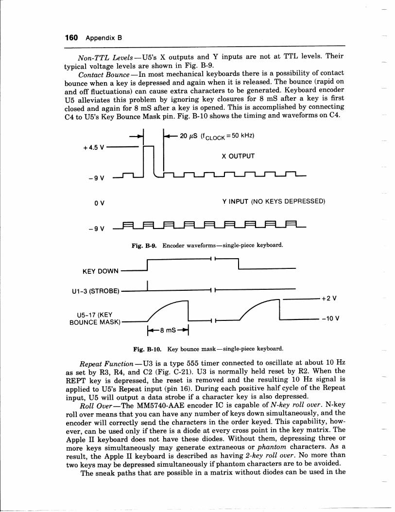
160 Appendix B
Non-TTL Leuels-lJ5's X outputs and Y inputs are not at TTL levels. Theirtypical voltage levels are shown in Fig. B-9.
Contact Bounce-Tn most mechanical keyboards there is a possibility of contact
bounce when a key is depressed and again when it is released. The bounce (rapid on
and off fluctuations) can cause extra characters to be generated. Keyboard encoder
Ub alleviates this problem by ignoring key closures for 8 mS after a key is firstclosed and again for 8 mS after a key is opened. This is accomplished by connecting
C4 to Ub's Key Bounce Mask pin. Fig. B-10 shows the timing and waveforms on C4.
20 pS (f cuocK = 50 kHz)
+4.5 V
-9 V
OV
-9 V
KEY DOWN
Y INPUT (NO KEYS DEPRESSED)
=EH-=l=l=l=l=l=lFig. B-9. Encoder waveforms-single-piece keyboard.
u1-3 (srRoBE) I ,
-+2Y
u5-17 (KEYB.'N.EMASK) 4 -1ov
f.-.a rs*|Fig. B-f0. Key bounce mask-single-piece keyboard.
Repeat Function-U3 is a type 555 timer connected to oscillate at about 10 Hz
as set by R3, R4, and C2 (Fie. C-2L). U3 is normally held reset by R2. When theREPT key is depressed, the reset is removed and the resulting 10 Hz signal isapplied to U5's Repeat input (pin 16). During each positive half cycle of the Repeat
input, U5 will output a data strobe if a character key is also depressed'RolI Ouer-The MM5740-AAE encoder IC is capable of N-key roll ouer. N-key
roll over means that you can have any number of keys down simultaneously, and theencoder will conectly send the characters in the order keyed. This capability, how-
ever, can be used only if there is a diode at every cross point in the key matrix. TheApple II keyboard does not have these diodes. Without them, depressing three ormoie keys simultaneously may generate extraneous or phantorn characters. As aresult, the Apple II keyboard is described as having Z-key roll ouer. No more thantwo keys may be depressed simultaneously if phantom characters are to be avoided.
The sneak paths that are possible in a matrix without diodes can be used in the
OUTPUT

Appendix B 161
single-piece keyboard to generate characters not normally available from thekeyboard as shown in Table B-2.
Table B-2. Generate Special Characters
I Hold down theseCharacter I keys simultaneously
(Underscore) I SHIFT, U, l, Y[ (Left Bracket) I SHIFT, U, l, J\ (Backslash) I SHIFT, U, l, H
With the proper editing, you can insert these characters into programs directly fromthe keyboard.
Quad-Mode Operation-U5 is a quad-mode encoder. This means each key cangenerate up to four different characters as a function of the SHIFT and CTRL keys(see Table B-3).
Table B-3. CHARACTERS as a Function of Control and Shiftu5-1 9 (CTRL) u5-21 (SHIFT) Character Group
001
1
01
01
UnshiftshiftControlShift-Control
The four characters for each key are shown in Fig. C-2L*. Only the "P," "M," and"N" keys can generate four different characters. The rest generate one or two.
Initialization-C7 and R8 form a delay circuit that initializes U5 on power upby taking SHIFT high for about 5 mS. Diode CRl provides a rapid discharge pathfor C7.

APPENDIX
Apple II Schematics
This appendix contains schematics for the Apple II mother board, keyboard, andpower supply. Mother board schematics are provided for circuits dating from theearliest Apple II to the most recent revision available for publication. The para-graphs that follow contain information intended to help you use the schematics.
REVTSTONS
Mother BoardsAs described in Appendix B, the earliest Apple II mother board is known as Rev. 0. Ashort time after the Apple's introduction, several circuit changes resulted in the Rev.1 mother board. Rev. 1 includes a color killer and two more HIRES colors. Therewere no more significant circuit changes until the introduction of the Rev. 7 motherboard. Rev. 7 deletes the Memory Jumper Blocks and changes the charactergenerator ROM. The next significant change involved modification of the motherboard and packaging to reduce RFI. Some minor circuit changes were made at thesame time. The major revisions of the mother board are denoted in this book as Rev.0, Rev. 1, Rev. 7, and RFI.
Appendix B contains additional information on the differences between revi-sions. It also describes how you can examine the mother board to determine therevision of a particular Apple II. Note that the circuit description in the body of thisbook corresponds to the RFI schematics. Material in Appendix B describes thedifferences in operation of Revisions 0, 1, and 7 relative to the operation of the RFImother board.
A notation on each schematic indicates the revision to which the schematicapplies. Most schematics apply to two or more revisions., Minor circuit differencesbLlween the revisions are indicated by notes or insets on the drawing. When thereare major differences between revisions, sepafate schematics are used for each revi-sion. As you trace a signal from schematic to pchematic, be sure to use the drawingthat corresponds to the revision of interest.
162

Appendix C 163
KeyboardsThe original Apple II keyboard was constructed on a single printed circuit board andis thus referred to as the "single-piece keyboard." Apple later introduced a "two-piecekeyboard." The two-piece keyboard contains one printed circuit board on which thekeys are mounted. A second printed circuit board containing the ICs then plugs ontothe first printed circuit board. This appendix contains schematics for both the single-and two-piece keyboards.
SYMBOLS
Fig. C-l shows some of the symbols used on the schematics. When a signal enters orexits a schematic, the signal name is shown beside an arrow symbol (Examples athrough d). The direction of the arrow indicates the direction of signal flow. Adouble-headed arrow indicates bidirectional signal flow, such as on a data bus(Example c). If the signal is part of the system bus, a number inside the arrowsymbol gives the peripheral VO connector pin on which the signal appears (Exam-ples c and d). A ((Tb" or "From" notation beside a signal name indicates the otherschematics on which the signal appears. The designations "Part 1" and "Part 2"refer to the two separate drawings used to show some schematics. For example, thevideo generator schematic is divided into two parts.
Logic functions that are active on a low level are shown by a small circle orEXAMPLE: FROM
cLocK I R(a) cENERAToR FqM I hl. t-----'--'-
(b)
(c)
(d)
(e)
(f)
(g)
(h)
(i)
FR.M t Do
MTCRoPROCESSO* I
Inru
CLOCKINPUT
rP4F
ACTIVE HIGH
ACTIVELOW
Fig. C-1. Schematic symbols.

164 Appendix C
"bubble." For example, see the Q output and CLR input in Example e. The symbol atpin 3 is a clock input.
The symbols in Examples f and g represent the shapes of printed circuit boardtraces that are meant to be altered in order to modify the circuit. The bow ti.e inExample f would be cut between the arrows to open the circuit. The semicircles inExample g would be bridged with solder to close the circuit.
A number in a square (Example h) refers to a note shown elsewhere on thedrawing. The symbol in Example i represents a test point or other labeled solderpoint on the circuit board.
When an IC is powered from *5 volts and ground, and these voltages connect tothe usual opposite corner pins of the IC, then the power pins are not shown on theschematic. If the *5 volts connects to an unusual pin or if the IC requires multiplevoltages, then the power pins are shown. In general, bypass capacitors, ferrite beads,and isolated grounds are not depicted in the drawings.
The Apple II schematics are shown in Figs. C-2* through C-23*.
ACKNOWLEDGMENTS
The schematics in this appendix have been used with the permission of Apple Com-puter, Inc. They have been redrawn from the following Apple Computer documents:
Revision 0Mother board
Apple II Reference Manual ("Red Book"),Jan. 1978
Revision 1
Mother board,Power Supply,Single-pieceKeyboard
Apple II Reference Manual , 1979
Revision 7
Mother boardThe Apple II Reuision 07 Main Board
RFIMother board
Addendum to the Apple II Reference Manual
TIvo-pieceKeyboard
Schematic, A-2 Keyboard & Encoder,Drawing No. 050-0021-D

APPENDIX
References
Chapter 1
1.1 Espinosa, Christopher. Apple II Reference Manual, Apple Computer, Inc., 1979.
t.2 The TTL Data Booh for Design Engineers,2nd, ed., Tbxas Instruments, 1976.
Chapter 22.1 United States Patent No. 4,130,862, "DC Power Supplyj'Inventor: Frederick R.
Holt, Assignee: Apple Computer, Inc., 19 Dec., 1978.2.2 Wozniak, Stephen. "System Description-The Apple IIi Byte, May t977.
Ghapter 3
3.1 United States Patent No. 4,136,359, "Microcomputer for use with Video Dis-play," Inventor: Stephen G. Wozniak, Assignee: Apple Computer, Inc., 23 Jan.,L979.
3.2 Wozniak, Stephen. "The Impossible Dream: Computing e to 116,000 Places witha Personal Computer,"Byte, June 1981.
Chapter 55.! Memory Data Book and Designers Guidc, Mostek, 1979.
Ghapter 6
6.1 "Apple II Product Specifications, Hobby/Prototyping Board," Apple Computer,Inc.
6.2 "Applications Information AN2-SY6500 Microprocessor Familyj' Microproces-
sor Products, Synertek, Jan. 1980.G.B DeJong, Marvin L. Programming & Interfacing the 6502, with Experiments,
Howard W. Sams & Co., Inc., 1980.
6.4 Fischer, Dan and Caffrey, Morgan P. "Go Ahead and Interrupt your Applel'Parts 1 and 2, Softalh, Mar. and Apr' 1982'
6.5 Holland, John M. Aduanced 6502 Interfacing, Howard W. Sams & Co., Inc.,
t982.
t-
165

166 Appendix D
6.6 MCS 6500 Microcomputer Family Hardware Manual, Commodore Business Ma-chines, Inc. (MOS Tbchnology), Jan. L976.
6.7 MCS 6500 Microcomputer Family Programming Manual, Commodore BusinessMachines, Inc. (MOS Tbchnology), Jan. 1976.
6.8 R6500 Mi,crocomputer System Hardware Manual, Rockwell International, Aug.1978.
6.9 "R6500 Microcomputer System Data Sheet," Rockwell International, Nov. 1981.6.10 R6500 Microcornputer System Prograrnming Manual, Rockwell International,
Feb. 1979.6.11 Scanlon, Leo J.6502 Software Design, Howard W. Sams & Co., Inc., 1980.6.12 "6500 Microprocessors" (Data Sheet), Commodore Semiconductor Group, Feb.
1981.6.13 Sy6500lMCS6500 Microcomputer Family Hardware Manual, Synertek, Aug.
L976.6.L4 SY6500lMCS6500 Microcomputer Family Programming Manuol, Synertek,
Aug. 1976.6.L5 SY6500 Data Sheet, "8-Bit Microprocessor Family," Synertek, Apr. 1980.6.16 Titus, Jonathan S., Larsen, David G., and Titus, Christopher A. Apple Interfac-
ing, Howard W. Sams & Co., Inc., 1981.6.17 White, George M. "Using Interrupts on the Apple II System," Byte, May 1981.
Chapter 77.L Apple II Monitors Peeled, Apple Computer, Inc., 1981.7.2 "AY-5-3600 Keyboard Encoder Operationj' Bulletin L402, General Instrument
Corp.7.3 Data Catalog, Standard Microsystems Corp., 1981 (KR3600 Keyboard Encoder).7.4 Lancaster, Don. TV fupewriterCookbook,Howard W. Sams & Co., Inc., 1976.7.5 Microelectronics Product Catalog, General Instrument Corp., 1980 (AY-5-3600
Data Sheet).7.6 "The Apple II Cassette Interface," Apple Orchard, Spring 1981.
Ghapter 8
8.1 Bishop, Bob. "Apple II HIRES Graphics: Resolving the Resolution Myth," AppleOrchard, Fall 1980.
8.2 Rowe, Pete. "The Mysterious Orange Vertical Line," Apple Orchard, Fall 1980.8.3 United States Patent No. 4,278,972,"Digitally Controlled Color Signal Genera-
tion Means for use with Display," Inventor: Stephen G. Wozniak, Assignee:Apple Computer, Inc., 14 July, 1981.
Appendix AA.1 Bierman, Howard and Bierman, Marvin. Color Teleuisinn Principles and Seruic-
ing, Haydert Book Co., Inc., L973.A.2 "EIA Tblevision Systems Bulletin No. 4, EIA Recommended Practice for Hori-
zontal Sync, Horizontal Blanking and Burst Timing in Tblevision Broadcast-ing," EIA, Mar. 1976.
A.3 "EIA Standard RS-170, Electrical Performance Standards-Monochrome Tble-vision Studio Facilities," EIA, Nov. 1957.
A.4 "EIA Standard RS-189-A, Encoded Color Bar Signal," EIA, July 1976.

Appendix D 167
A.5 "EIA Standard RS-330, Electrical Performance Standards for Closed CircuitTblevision Camera 525160Interlaced 2:Ll' EIA, Nov. 1966.
A.6 Grob, Bernard, Basic Teleuision Principles and Seruicing,McGraw-Hill, L975.A.7 "Industrial Electronics Bulletin No. 1, Closed Circuit Tblevision-Definitionsi'
Electronics Industries Association, Sept. 1962.A.8 "19-Inch Color TV's," Consumer Reports, Jan. 1981.A.9 Schure, Alexander. Basic Teleuision, Vol. 6, Hayden Book Co., Inc., 1975.
Appendix B
B.l- "Addendum to the Apple II Reference Manuali' Apple Part No. 031-0004-8,Apple Computer, Inc. (Reduced RFI Mother Board)'
8.2 Appte II Reference Manual (Red Book), Apple Computer, Inc., Jan. 1978.
B.3 "Application Note AN-80, MOS Keyboard Encoding," National SemiconductorCorp., April L973.
B.4 "Data Sheet, MM5740 90-Key Keyboard Encoder," National SemiconductorCorp., 1977.
8.5 "The Apple II Revision 07 Main Boardj' Apple Part No. 031-0072-00, AppleComputer, Inc.
B.6 *2513 Data Sheet-High Speed 64 x 7 x 5 Character Generatorl' Signetics.
hdexAccess Card, peripheral, 68
6502,53 Cassettetime,42 input, 152
Accidental reset, 93 tape, 87, 93-96Address, 58 Cells, 105
bus, 17-18,58 Charactercolumn, 42 generator, t24-L26, L52decoding, 62-63 keys,88high-order, 18 Check sum, 93low-order, 18 Clear interrupt disable bit (CLI), 78multiplex (AX), 57 Clock(s), L8,24-25,59-60multiplexed,,42 basic, 26multiplexing,44-45,52-55 generator, 26-27video, 20 block diagram, 25-26
Addressable latch, 103 microprocessor, 27Architecture, L7 synchronization, 30, 33Array, memory, 44,47-49 ColorASCII burst, 35,40
null, 93 generation, HIRES, 130space, 93 LORES, 134
Asynchronous, 78 killer, 151, 153Auxiliary video pin, 152 Rev. 1, 152
REF, 25tv, L42-146
B wheel, 112Column
Bidirectional, 59 address, 42Binary addition, 54 strobe (CAS), 42Black, lLl,120 Combinatorial logic, 37-38Blanked, 140 Comparator, 96Blanking, 35, 38 Composite video, 40, 139
interval, 117 Connector, peripheral,63level, 140 Contact bounce, 160signal, 111 Control, 59vertical, 140 bus, 18
Block diagram, clock generator, 25-26 Copyrights, 10Blue, 112 Counter overflow, 100Bow tie, 164 CR3, 33Broadcast standards, l4L-142 CR4, 33Burst, LLz, L44 CycleBuses, 17 extended, 29-30
168
CA

lndex 169
Cycle (continued)
read, 42, 47 -49write, 42-43, 49
D
Daisychain(s), 64
DMA,73-75interrupt, 77
Dark blue, L20, 136Darlington pair, 96Data, 47, 58-59
bus, 18, 58in (DI), 42out (DO), 42path, 46, 47 -49strobe output, 90transceiver, I52
Decoditg, address, 62-63DeMorgan's theoreffi, 37Device select, 68Direct memory access (DMA),Display modes, 19DL7 effects, 130DMA
daisy chain, 73-75read from RAM, 75-76write to RAM, 76
Dot matrix characters, L24Dynamic, 4L
E
Early-write, 42cycle, 49
Edge-sensitive, 61Enable, 37Encoder IC, keyboard, 88-90Equalizing interval, L4LEuropean tv, 35, 153Even
byte timing, L29-130, I34character timing, L27
Extended cycle, 29-30
F
Feedbackpath, 20signal, 20
Filter, video, L52Flash/inverse signal, 110Flashing character, L26Flip-flop, 1114IL6 dynamic RAM, 4L-434-bit adder, 46Four HIRES colors, 153Frame, LALFull address decode, 68
G
Gameconnector, 87-88paddles, 98-103switches, 97-98
Generatorcharacter, L24-L26
1g clock, 26-27sync, 2Lvideo, 2L
address, 20, 26Gloss dty, L2-L6Gray, L20Green, 113
H
Header tone, 93High-order address, 18HIRES, 111-116
and text, mixed, L21-123, 136-138color generation, 130mode, 19, L28-L32
circuit configuration, L28-L29timing diagr&D, I29
Holdstate, 63time, 42
Horizontalblanking (HBL), 38sync, L40timing, 27-29
170 lndex
H2 inverter, L52Hue, 35, II2, L44
I
ICkeyboard encoder, 88-90, 158nomenclature, 11
Impedance, high, L2Inhibit (INH), 63Initialtzattor, 161Input/output, L9-20Interl ace, L4IInterrupt(s), 77 -7 8
daisy chain, 77(IRQ and NMI), 60-61request (IRQ, 18sequence , 7 8
Inverse video, L26VO
select, 68strobe, 68
K
Keyboard, 64, 86-87, 151encod€r, 90
IC, gg-90, 159read from, 70-7Lsingle-piece, 158-161two-piece, 88-93
L
Level(s)non-TTL, 90sensitive,6l
Lightblue, 119emitting diode (LED), 23
Logiccombinatorial, 37-38three state, L2
LORES, 116- LzLand text, mixed, L23, 138color generation, I34
LORES (continued)mode, 132-L36
circuit configuration, L32-133timing diagram, L34
Low-order address, 18Lowercase operation, 93Luminance, L42
M
Mappirg, 52-55video memoty, 45-46
Maskable, 61Medium blue, 119Memoty, 18
array, 44, 47 -49cell , 4Ijumper blocks, I52mapper, 20-2Imappirg, video, 45-46
Microprocessor, 17clock, 276502, 5g-64
MIX MODE, 19Mother board revisions , L49-151Multiplexed address, 42Multiplexing, address, 44-45, 52-55Mysterious orange line , L32
N
Non- maskable, 61
interrupt (NMI), 18
-RFI mother boards, 150-151
- TTL levels, 90Numeric pad, 93
o
oddbyte timing, 130, I34character timing, 128
On-board TlO, 19Oran ge, 113Output
high, 12low, L2

lndex 171
Overscan, L47Overvoltage, 23
P
Paddl€s, game, 98-103Page
1 HIRES, 551 Text, 532, 192 HIRES, 572 Text, 55
Patents, 10Peripheral
card, 68connector, 68I/O, 19read from, 68-70write to, 7 0
Phantom(s), 91-93characters, 92
Phase I,602, 600, 60
Pixel , 52, I04Power
on reset, 153supply, 2I-23
a
Quad-mode operation, 92, 161
R
RAM, 19address 6 termination, L52read from, 64-66write to, 66
Random access memory (RAM), 18Read
cycle , 42, 47 -496502, 62
from I/O, 19keyboard, 6502, 70-7Iperipheral , 6502, 68-70RAM, DMA, 75-76
6502, 64-66ROM, 6502, 66-67
Read (continued)modify-write, 42only memory (ROM), 18write (R/W), 47, 60
Ready, 60line, 73
Reclock, L28Refresh, 4I, 46, 57Regulation, power supply, 2L-23Repeat function, 90-91, 160Research, 12Reset, 61 , 78
power-or, 153Retrace, vertical, I40Return from interrupt (RTI), 78Revision(s), 11
1 non-RFI mother board, 152-1537 non-RFI mother board, 15L-L520 non-RFI mother board, 153-L57
RFI mother boards, 151Roll over, 91-93, 160ROM, 18-19
read from, 66-67Row address strobe (RAS), 25, 42
S
Saturation, L44Scope loop, 6502, 80-85Serrations, L40Set overflow, 62shift
regist€r, 111A3, L26c2,26
Signal14M, 25high, L2low, 12nomenclature, 11
7M,25Single-piece keyboard, 151, 158- 1616502
access, 53microprocessor, 58-64read cycle, 62
from keyboard, 70-7Iperipheral, 68-70RAM,64-66ROM,66-67

172 lndex
6502 (continued)'scope loop, 80-85write cycle, 62
to peripheral , 70RAM,66
Slot 7, 155Soft
5, L52switches, 19, 88, 103
Solder pad 7, L52Speaker, 87,96Standards, broadcast, L4L-L42Strobe delay, 90Subcarrier, L42Switches
game, 97-98soft, 103
Switching power supply, 2LSync, 38, 61
bit, 93generator, 2Lvideo, 35, 155
Synchronization of clocks, 30,Synchronous, 7 5
T
Test connector, I52Text, 108-111
and HIRES, mixed, 136-138LORES, mixed, 138
flashing, L26inverse, L26mode, 19, L24-L28
circuit configuration, L26timing diagr&ffi, L26-L27
normal, L26points, L52
Three-state logic, L2Timing
diagram, HIRES mode, I29LORES, T34text mode, L26-L27
even byte, L29-130, L34character, L27
horizontal , 27 -29odd byte, 130, L34
character, L28vertical, 34-35
Tbademarks, 10TV
Furopean, 35standards, European, 153
24K memory size probl€ffi, 153TIvo-piece keyboard, 88-93, 151
U
Undirectional, 58USER 1, 72-73
V
vA, 35, 37VB, 37Vertical
blankirg, L40retrace, 140
BB sync, L40, I52timing, 34-35
Video, 20-2Laddress generator, 20, 26composite, 40, 139display, basic, 139-140filter, L52generator, 2Iinverse, L26memory mapping, 45-46pin, auxiliary, L52, 155sync, 35, 153, 155
Violet, ILz
w
Wait-states, 58Waveforms, L2White, 115, I20
picture level , L40Write (WR), 42
cycle, 42-43, 496502, 62
to I/O, 19peripheral , 6502, 70RAM, DMA,76
6502, 66

=,. sAMs APPLE@ BooKs
Many thanks for your interest in this Sams Book about Apple llo microcomputing. Here are a fewmore Apple-oriented Sams products we think you'll like:
POLISHING YOUR APPLE@Clearly written, highly practical, concise assembly of all procedures needed for writing, disk-filing,and printing programs with an Apple ll. Positively ends your searches through endless manuals tof ind the routine you need! By Herbert M. Honig. Approximately 64 pages, 5lz x 8lz, comb. ISBN0-672-22026-1. O 1982.Ask lor No. 22026 . . . . $4.95 Tentative
THE APPLE !I@ CIRCUIT DESCRIPTIONProvides you with a detailed circuit description of the Revision 1 Apple ll motherboard, including thekeyboard and power supply. Compares Revision 1 with other revisions, and includes timing diagramsfor major signals. By Winston D. Gayler. Approximately 240 pages, 8Vz x 11, comb. ISBN0-672-21959-X. @ 1983.Ask lor No.21959 . . .$22.95 Tentative
INTERMEDIATE LEVEL APPLE IIO HANDBOOKHands-on aid for exploring the entire internal firmware of your Apple ll and f inding out what you canaccomplish with its 6502 microprocessor through machine- and assembly-language programming.By David L. Heiserman. Approximately 364 pages, 6 x 9, comb. ISBN 0-672-21889-5. @ 1983.Ask for No.21889 . . . . $9.95 Tentative
APPLE@ FORTRANOnly fully detailed Apple FORTRAN manual on the market! ldeal for Apple programmers of all skilllevels who want to try FORTRAN in a business,or scientific program. Many ready-to-run programsprovided. By Brian D. Blackwood and George H. Blackwood. 240 pages, 6 x 9, comb. ISBN0-672-21911-5. @ 1982.AsklorNo.21911 ......$14.95APPLE IIO ASSEMBLY LANGUAGE -[.J.Shows you how to use the 3-character, 56-word vocabulary of Apple's 6502 to create powerful, fast-acting programs! For beginners or those with little or no assembly language programming experi'ence. By Marvin L. De Jong.336 pages, 5Vz x81h, soft. ISBN 0'672'21894'1. O 1982.AsklorNo.21894. ' '...$15.95ENHANCING YOUR APPLE ll@ - Vol. IShows you how to mix text, LORES, and HIRES anywhere on the screen, how to open up whole newworlds of 3-D graphics and special effects with a one-wire modification, and more. Tested goodiesfrom a trusted Sams author! By Don Lancaster. 232 pages, 81/z x11, soft. ISBN 0-672-21846-1. O 1982.AsklorNo.21846. .....$15.95
CIRCUIT DESIGN PROGRAMS FOR THE APPLE IP-[-I.Programs quickly display "what happens if" and "what's needed when" as they apply to periodicwav-eform, ims and average values, design of matching pads, attenuators, and heat sinks, solution ofsimultaneous equations, and more. By Howard M. Berlin. 136 pages, SVz x 11, comb. ISBN0-672-21863-1. O 1982.AskforNo.21863. ... '.$15.95
APPLE@ TNTERFAcTNG -[J.Brings you real, tested interfacing circuits that work, plus the necessary BASIC software to connectyour Apple to the outside world. Lets you control other devices and communicate with other com-puters, modems, serial printers, and more! By Jonathan A. Titus, David G. Larsen, and Christopher A.Titus. 208 pages, 51/z x81h, soft. ISBN 0-672-21862'3. O 1981.AskforNo.21862. . '.. '$10.95

INTIMATE INSTRUCTIONS IN INTEGER BASICExplains flowcharting, loops, functions, graphics, variables, and more as they relate to lntegerBASIC. Used with Applesoft Language (No. 21811), it gives you everything you need to programBASIC with your Apple ll or Apple ll Plus. By Brian D. Blackwood and George H. Blackwood. 160pages, 51h xBVz, soft. ISBN 0-672-21812-7. O 1981.AskforNo.21812. ......$8.95APPLESOFT@ LANGUAGEOnly complete text available on Applesoft BASIC! Self-teaching format simplifies learning and letsyou use what you learn FAST. ldeal for businessmen, hobbyists, and professionals! Many programsincluded. By Brian D. Blackwood and George H. Blackwood. 256 pages, 5lz x $Vz, soft. ISBN0-672-21811-9. O 1981.AsklorNo.21811 ......$10.95MOSTLY BASIC: APPLICATIONS FOR YOUR APPLE ll@, BOOK 1
Twenty-eight debugged, fun-and-serious BASIC programs you can use immediately on your Apple ll.lncludes a telephone dialer, digital stopwatch, utilities, games, and more. By Howard Berenbon. 160pages, 81/z x 11, comb. ISBN 0-672-21789-9. @ 1980.AskforNo.21789. .....$12.95
MOSTLY BASIG: APPLICATIONS FOR YOUR APPLE llo, BOOK 2A second gold mine of fascinating BASIC programs for your Apple ll, featuring 3 dungeons, 11 house-hold programs, 6 on money or investment, 2 to test your ESP level, and more - 32 in all! By HowardBerenbon. 224 pages,81h x 11, comb. ISBN 0-672-21864-X. O 1981.AskforNo.21864-. '.. '$12.95
You can usually find these Sams products at better computer stores, bookstores, and electronicdistributors nationwide.
lf you can't find what you need, call Sams at 800-428-3696 toll-free or 317-298-5566, and charge it toyour MasterCard or Visa account. Prices subject to change without notice.
For a free catalog of all Sams Books available, write P.O. Box 7092, lndianapolis lN 46206.
SAMS BRINGS YOU MIND TOOLSTM FOR FINANCIAL PLANNING IN BUSINESSSpecial, ready-to-use software that temporarily interlocks with the spreadsheet in your regular ver-sion of Multiplano or VisiCalc@ so you can immediately perform 17 common financial planning cal-culations without wasting time manually setting up the sheet. All you do is enter the data - theproper formulas and column headings are there automatically!
Mind Tools allow you to instantly calculate present, net present, and future values, yields, internaland financial management rates of return, and basic statistics.
Also lets you do break-even analyses, depreciation schedules, and amortization tables, as well ascompute variable- and graduated-rate mortgages, wraparound mortgages, and more!
Allows you to use your regular spreadsheet as you always have, at any time. ldeal for any business-man with financial planning responsibilities, as well as for business students and instructors.
Supplied with complete documentation, including 136-page text and 68-page quick-reference guide,all in a binder with the proper disk to match the brand of spreadsheet program you own.
Currently available for use with Multiplan or VisiOalc on the Apple ll as follows:
EXECUTIVE PLANNING WITH MULTIPLANApple ll Version, ISBN 0-672-22058-X.AsklorNo.22058. .....$59.95
EXECUTIVE PLANNING WITH VISICALCApple ll Version, ISBN 0-672-22059-8.AskforNo.22059. .....$59.95

TO THE READERSams Computer books cover Fundamentals - Programming - lnterfacing - Technology written to meet theneeds of computer engineers, professionals, scientists, technicians, students, educators, business owners, per-
sonal computerists and home hobbyists.
Our Tradition is to meet your needs and in so doing we invite you to tell us whatyour needs and inferesfs are by completing the following:
1. t need books on the following topics:
2. I have the following Sams titles:
3. My occupation is:
Scientist, Engineer
Personal computerist
Technician, Serviceman
Educator
Student
D P Professional
Business owner
Computer store owner
Home hobbyist
Other
Name (print)
Address
City
Mail to: Howard W. Sams & Co., lnc.Marketing Dept. #CBS1/804300 W. 62nd St., P.O. Box 7092lndianapolis, lndiana 46206
State zip
2 t959


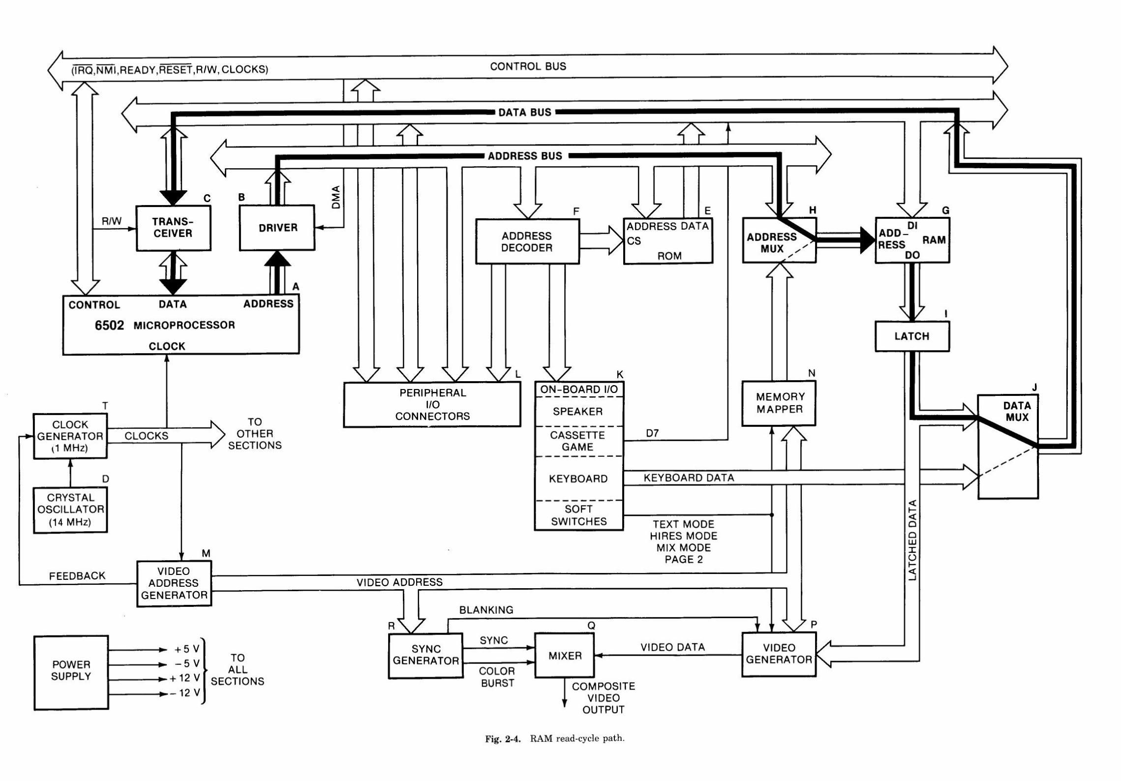


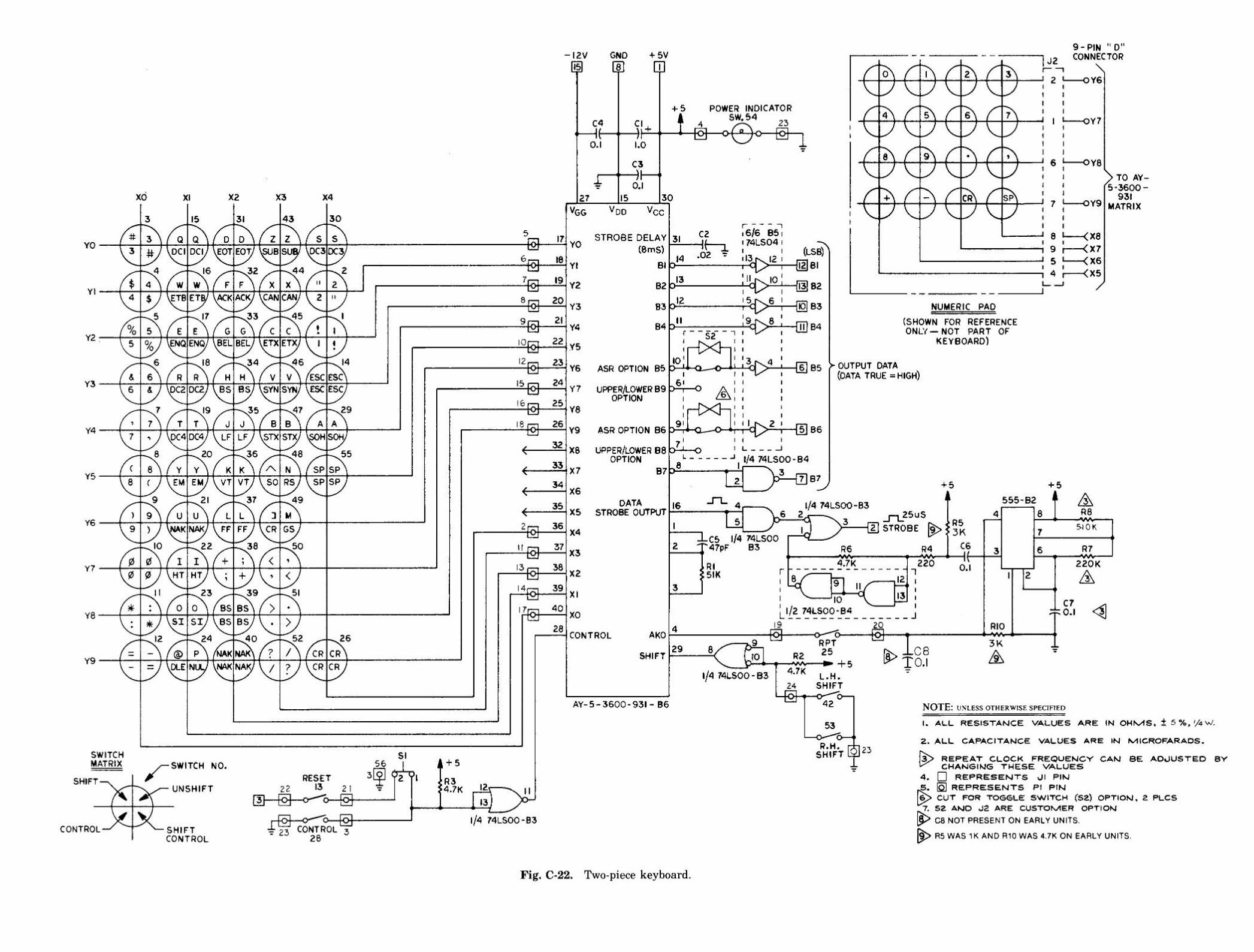

*.,
THEFPLE ll'CIRCUIT DESGRIPTION
o Covers all Apple ll@ motherboard and keyboard revisions!r Helps you learn about microcomputer hardware in general and Apple ll@ hard-
ware in detail!o Provides you with accurate schematics and verified waveforms to rely on for
servicing and repair!o Explains the advanced concepts of daisy chains, interrupts, direct memory
access, and the ready line!o Gives you many valuable hints for successful interfacing!o Contains tutorials on video signals, memory lCs, and the 6502 microprocessor,
as well as full explanations of advanced concepts!r Each chapter contains an overview for the beginner and a detailed section for
the more adventurous!r ldeal for students, technicians, hobbyists, engineers, and others who need
Apple ll@ technical information!
I
i
II
I
:
I
I
-,I
q
-
-
-?
Winston D. Gayler is a design engineer and consultant specializing inmicrocomputeis and digital telephony. He received his Bachelor ofScience and Master of Engineering degrees from Cornell University.Now a resident of silicon Valley, Mr. Gayler is a member of the AudioEngineering Society, the lnstitute of Electrical and Electronic Engineers,and is also-a California Registered Professional Engineer. He haspresented technical papers to the IEEE. His work in digital telephonyhas been published in IEEE and other conference proceedings.
HOWARDI'V. SAMS & CO., INC.4300 West 62nd Street, lndianapolis, lndiana 46268 USA
I
-(
-
"^
Ef!
\
-ISBN i O-672-21959-X