voxtel apd catalog
DESCRIPTION
Voxtel product and services calalogTRANSCRIPT

N I R A v a l a n c h e P h o t o d i o d e s
P h o t o r e c e i v e r s
C A T A L O G
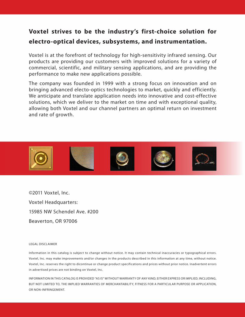
Voxtel is at the forefront of technology for high-sensitivity infrared sensing. Our products are providing our customers with improved solutions for a variety of commercial, scientific, and military sensing applications, and are providing the performance to make new applications possible.
The company was founded in 1999 with a strong focus on innovation and on bringing advanced electo-optics technologies to market, quickly and efficiently. We anticipate and translate application needs into innovative and cost-effective solutions, which we deliver to the market on time and with exceptional quality, allowing both Voxtel and our channel partners an optimal return on investment and rate of growth.
©2011 Voxtel, Inc.
Voxtel Headquarters:
15985 NW Schendel Ave. #200
Beaverton, OR 97006
LEGAL DISCLAIMER
Information in this catalog is subject to change without notice. It may contain technical inaccuracies or typographical errors.
Voxtel, Inc. may make improvements and/or changes in the products described in this information at any time, without notice.
Voxtel, Inc. reserves the right to dicontinue or change product specifications and prices without prior notice. Inadvertent errors
in advertised prices are not binding on Voxtel, Inc.
INFORMATION IN THIS CATALOG IS PROVIDED “AS IS” WITHOUT WARRANTY OF ANY KIND, EITHER EXPRESS OR IMPLIED, INCLUDING,
BUT NOT LIMITED TO, THE IMPLIED WARRANTIES OF MERCHANTABILITY, FITNESS FOR A PARTICULAR PURPOSE OR APPLICATION,
OR NON-INFRINGEMENT.
Voxtel strives to be the industry’s first-choice solution for
electro-optical devices, subsystems, and instrumentation.
Contents
APD Product Guide 4
Voxtel APDs 6
Introduction 6
Product Series 6
Responsivity vs. Noise 8
Comparison Table 9
APD Product Listings 12
Avalanche Photodiodes 12
Packaged APDs 23
APD Photoreceivers 37
APD Receiver Support Electronics Modules 52
References 53
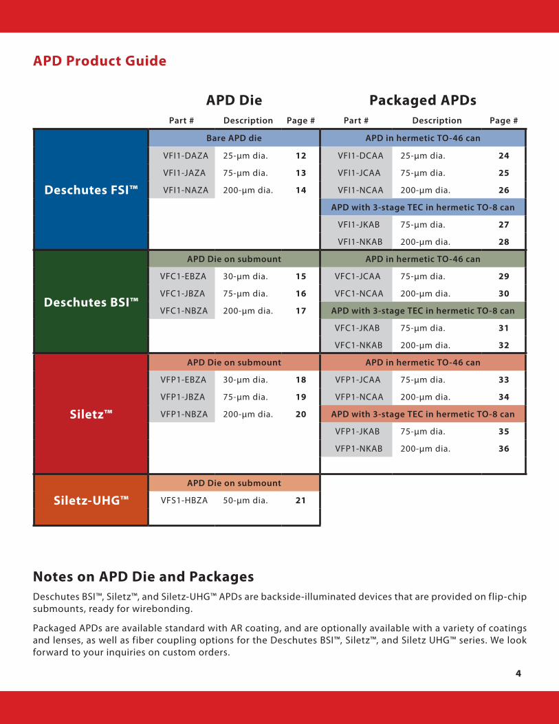
4
APD Die Packaged APDs APD PhotoreceiversPart # Description Page # Part # Description Page # Part # Bandwidth Description Page #
Deschutes FSI™
Bare APD die APD in hermetic TO-46 can
Deschutes FSI™
Window-coupled Receivers in hermetic TO-8 can
VFI1-DAZA 25-µm dia. 12 VFI1-DCAA 25-µm dia. 24 RDI1-NJAC 200 MHz 200-µm dia. APD 39
VFI1-JAZA 75-µm dia. 13 VFI1-JCAA 75-µm dia. 25 RDI1-JJAC 580 MHz 75-µm dia. APD 40
VFI1-NAZA 200-µm dia. 14 VFI1-NCAA 200-µm dia. 26
APD with 3-stage TEC in hermetic TO-8 can
VFI1-JKAB 75-µm dia. 27
VFI1-NKAB 200-µm dia. 28
Deschutes BSI™
APD Die on submount APD in hermetic TO-46 can
Deschutes BSI™
Window-coupled Receivers in hermetic TO-8 can
VFC1-EBZA 30-µm dia. 15 VFC1-JCAA 75-µm dia. 29 RJC1-NJAC 200 MHz Band-limited receiver, 200-µm dia. APD 41
VFC1-JBZA 75-µm dia. 16 VFC1-NCAA 200-µm dia. 30 RDC1-NJAC 300 MHz 200-µm dia. APD 42
VFC1-NBZA 200-µm dia. 17 APD with 3-stage TEC in hermetic TO-8 can RIC1-JJAC 2 GHz 75 µm dia. APD 44
VFC1-JKAB 75-µm dia. 31 Fiber-coupled Receivers, TO-8 package
VFC1-NKAB 200-µm dia. 32 RIC1-JJQC 2 GHz 62.5/125 µm FO, others available 45
Siletz™
APD Die on submount APD in hermetic TO-46 can
Siletz™
Window-coupled Receivers in hermetic TO-8 can
VFP1-EBZA 30-µm dia. 18 VFP1-JCAA 75-µm dia. 33 RIP1-NJAC 1 GHz 200-µm dia. APD 46
VFP1-JBZA 75-µm dia. 19 VFP1-NCAA 200-µm dia. 34 RIP1-JJAC 2.1 GHz 75-µm dia. APD 47
VFP1-NBZA 200-µm dia. 20 APD with 3-stage TEC in hermetic TO-8 can Ball-lens-coupled Receivers, TO-8 package
VFP1-JKAB 75-µm dia. 35 R2P1-JCAA 1.5 GHz 300-µm dia. (effective) APD 49
VFP1-NKAB 200-µm dia. 36 Fiber-coupled Receivers, TO-8 package
RIP1-JJQC 2.1 GHz 62.5/125 µm FO, others available 51
Siletz-UHG™APD Die on submount
VFS1-HBZA 50-µm dia. 21
APD Product Guide
Notes on APD Die and PackagesDeschutes BSI™, Siletz™, and Siletz-UHG™ APDs are backside-illuminated devices that are provided on flip-chip submounts, ready for wirebonding.
Packaged APDs are available standard with AR coating, and are optionally available with a variety of coatings and lenses, as well as fiber coupling options for the Deschutes BSI™, Siletz™, and Siletz UHG™ series. We look forward to your inquiries on custom orders.
5
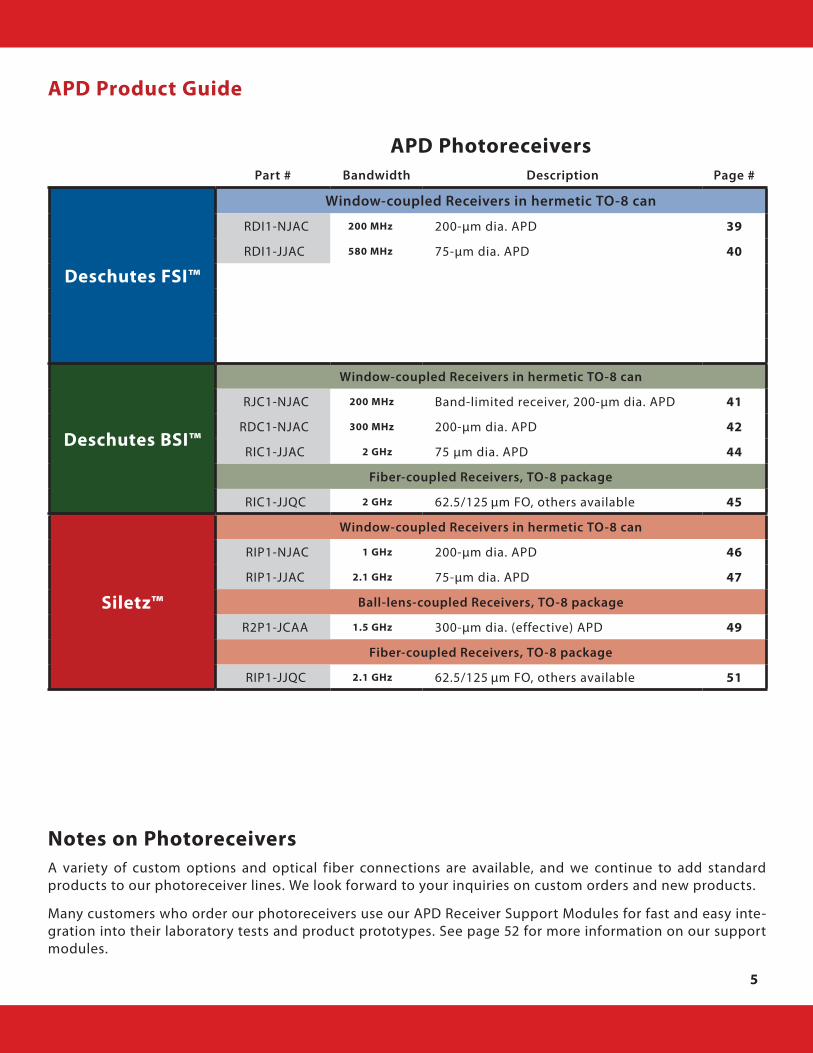
APD Die Packaged APDs APD PhotoreceiversPart # Description Page # Part # Description Page # Part # Bandwidth Description Page #
Deschutes FSI™
Bare APD die APD in hermetic TO-46 can
Deschutes FSI™
Window-coupled Receivers in hermetic TO-8 can
VFI1-DAZA 25-µm dia. 12 VFI1-DCAA 25-µm dia. 24 RDI1-NJAC 200 MHz 200-µm dia. APD 39
VFI1-JAZA 75-µm dia. 13 VFI1-JCAA 75-µm dia. 25 RDI1-JJAC 580 MHz 75-µm dia. APD 40
VFI1-NAZA 200-µm dia. 14 VFI1-NCAA 200-µm dia. 26
APD with 3-stage TEC in hermetic TO-8 can
VFI1-JKAB 75-µm dia. 27
VFI1-NKAB 200-µm dia. 28
Deschutes BSI™
APD Die on submount APD in hermetic TO-46 can
Deschutes BSI™
Window-coupled Receivers in hermetic TO-8 can
VFC1-EBZA 30-µm dia. 15 VFC1-JCAA 75-µm dia. 29 RJC1-NJAC 200 MHz Band-limited receiver, 200-µm dia. APD 41
VFC1-JBZA 75-µm dia. 16 VFC1-NCAA 200-µm dia. 30 RDC1-NJAC 300 MHz 200-µm dia. APD 42
VFC1-NBZA 200-µm dia. 17 APD with 3-stage TEC in hermetic TO-8 can RIC1-JJAC 2 GHz 75 µm dia. APD 44
VFC1-JKAB 75-µm dia. 31 Fiber-coupled Receivers, TO-8 package
VFC1-NKAB 200-µm dia. 32 RIC1-JJQC 2 GHz 62.5/125 µm FO, others available 45
Siletz™
APD Die on submount APD in hermetic TO-46 can
Siletz™
Window-coupled Receivers in hermetic TO-8 can
VFP1-EBZA 30-µm dia. 18 VFP1-JCAA 75-µm dia. 33 RIP1-NJAC 1 GHz 200-µm dia. APD 46
VFP1-JBZA 75-µm dia. 19 VFP1-NCAA 200-µm dia. 34 RIP1-JJAC 2.1 GHz 75-µm dia. APD 47
VFP1-NBZA 200-µm dia. 20 APD with 3-stage TEC in hermetic TO-8 can Ball-lens-coupled Receivers, TO-8 package
VFP1-JKAB 75-µm dia. 35 R2P1-JCAA 1.5 GHz 300-µm dia. (effective) APD 49
VFP1-NKAB 200-µm dia. 36 Fiber-coupled Receivers, TO-8 package
RIP1-JJQC 2.1 GHz 62.5/125 µm FO, others available 51
Siletz-UHG™APD Die on submount
VFS1-HBZA 50-µm dia. 21
APD Product Guide
Notes on PhotoreceiversA variety of custom options and optical fiber connections are available, and we continue to add standard products to our photoreceiver lines. We look forward to your inquiries on custom orders and new products.
Many customers who order our photoreceivers use our APD Receiver Support Modules for fast and easy inte-gration into their laboratory tests and product prototypes. See page 52 for more information on our support modules.

6
Voxtel APDs — Introduction
Voxtel APDs
Voxtel’s avalanche photodiodes (APDs) offer superior response and linear-mode, low-light-level detection capabilities that conventional telecommunications APDs and Geiger-mode APDs can’t offer.
Customers with applications that are presently served by NIR photodiodes or low-gain telecom APDs will often prefer the Deschutes FSI™ or Deschutes BSI™ APDs and photoreceivers for their modest price and low-noise performance at gains up to M = 20. A variety of high-performance and low-light-level applications are best served by our Siletz™ line of products, and our Siletz UHG™ line offers ultra-high gain and responsivity for the detection of very low light levels, including Voxtel’s published results in photon number discrimination (see page 53).
Voxtel’s single-element devices are available as bare die, on submounts (for our backside-illuminated prod-ucts), in hermetic packages, and integrated into photoreceivers, with a variety of options for packaging and optical input.
Voxtel’s APD Product Series
Silicon vs Voxtel’s InGaAs APDs
Voxtel produces a number of high-performance InGaAs APDs, and each is best suited for a particular range of applications. This guide discusses the differences between Voxtel’s products and related products for NIR detection, as well as the differences among Voxtel’s product lines.
Voxtel’s APDs are replacing silicon APDs in many applications. Silicon APDs are typically used for the 300–1100 nm spectral band, while InGaAs APDs normally cover the 900–1700 nm band. Their response overlaps in the 900–1100 nm spectral region, which includes the ubiquitous 1064 nm Nd:YAG solid-state laser line that is used in many systems for range finding and target designation.
Voxtel’s InGaAs APDs are often an attractive alternative to silicon APDs in designing new systems where a fast signal rise time is required, and have served many users of silicon APDs in migrating to eye-safe systems at e.g. 1550 nm while maintaining backwards compatibility with legacy 1064 nm illuminators. However, the detector specifications can be considerably different for the two types of APDs, so depending on the application, it may not be feasible to use an InGaAs APD as a drop-in-replacement for legacy systems using a silicon APD.
Voxtel’s InGaAs APDs are often the best choice for low-light-level and/or high-bandwidth applications, though understanding the differences between our detectors is important in order to choose the right Voxtel APD for a particular application.
Introduction Product Series
7
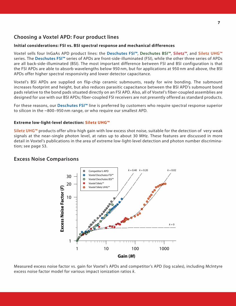
Choosing a Voxtel APD: Four product lines
Excess Noise Comparisons
Initial considerations: FSI vs. BSI spectral response and mechanical differences
Extreme low-light-level detection: Siletz UHG™
Voxtel sells four InGaAs APD product lines: the Deschutes FSI™, Deschutes BSI™, Siletz™, and Siletz UHG™ series. The Deschutes FSI™ series of APDs are front-side-illuminated (FSI), while the other three series of APDs are all back-side-illuminated (BSI). The most important difference between FSI and BSI configuration is that the FSI APDs are able to absorb wavelengths below 950 nm, but for applications at 950 nm and above, the BSI APDs offer higher spectral responsivity and lower detector capacitance.
Voxtel’s BSI APDs are supplied on flip-chip ceramic submounts, ready for wire bonding. The submount increases footprint and height, but also reduces parasitic capacitance between the BSI APD’s submount bond pads relative to the bond pads situated directly on an FSI APD. Also, all of Voxtel’s fiber-coupled assemblies are designed for use with our BSI APDs; fiber-coupled FSI receivers are not presently offered as standard products.
For these reasons, our Deschutes FSI™ line is preferred by customers who require spectral response superior to silicon in the ~800–950 nm range, or who require our smallest APD.
Siletz UHG™ products offer ultra-high gain with low excess shot noise, suitable for the detection of very weak signals at the near–single photon level, at rates up to about 30 MHz. These features are discussed in more detail in Voxtel’s publications in the area of extreme low-light-level detection and photon number discrimina-tion; see page 53.
1 10 100 1000
10
20
30
1
Gain (M)
Exce
ss N
oise
Fac
tor (F)
Competitor’s APDVoxtel Deschutes FSI™
Voxtel Deschutes BSI™
Voxtel Siletz™Voxtel Siletz UHG™
k = 0.40 k = 0.20 k = 0.02
k = 0
Measured excess noise factor vs. gain for Voxtel’s APDs and competitor’s APD (log scales), including McIntyre excess noise factor model for various impact ionization ratios k.
8
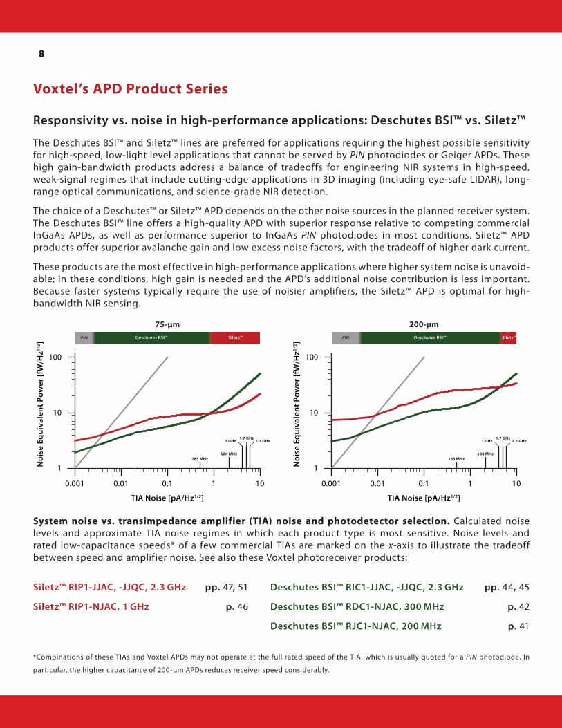
Responsivity vs noise in high-performance applications: Deschutes BSI™ vs Siletz™
The Deschutes BSI™ and Siletz™ lines are preferred for applications requiring the highest possible sensitivity for high-speed, low-light level applications that cannot be served by PIN photodiodes or Geiger APDs. These high gain-bandwidth products address a balance of tradeoffs for engineering NIR systems in high-speed, weak-signal regimes that include cutting-edge applications in 3D imaging (including eye-safe LIDAR), long-range optical communications, and science-grade NIR detection.
The choice of a Deschutes™ or Siletz™ APD depends on the other noise sources in the planned receiver system. The Deschutes BSI™ line offers a high-quality APD with superior response relative to competing commercial InGaAs APDs, as well as performance superior to InGaAs PIN photodiodes in most conditions. Siletz™ APD products offer superior avalanche gain and low excess noise factors, with the tradeoff of higher dark current.
These products are the most effective in high-performance applications where higher system noise is unavoid-able; in these conditions, high gain is needed and the APD’s additional noise contribution is less important. Because faster systems typically require the use of noisier amplifiers, the Siletz™ APD is optimal for high-bandwidth NIR sensing.
System noise vs. transimpedance amplifier (TIA) noise and photodetector selection. Calculated noise levels and approximate TIA noise regimes in which each product type is most sensitive. Noise levels and rated low-capacitance speeds* of a few commercial TIAs are marked on the x-axis to illustrate the tradeoff between speed and amplifier noise. See also these Voxtel photoreceiver products:
*Combinations of these TIAs and Voxtel APDs may not operate at the full rated speed of the TIA, which is usually quoted for a PIN photodiode. In
particular, the higher capacitance of 200-µm APDs reduces receiver speed considerably.
Siletz™ RIP1-JJAC, -JJQC, 2 3 GHz pp 47, 51
Siletz™ RIP1-NJAC, 1 GHz p 46
Deschutes BSI™ RIC1-JJAC, -JJQC, 2 3 GHz pp 44, 45
Deschutes BSI™ RDC1-NJAC, 300 MHz p 42
Deschutes BSI™ RJC1-NJAC, 200 MHz p 41
TIA Noise [pA/Hz1/2]
Noi
se E
quiv
alen
t Pow
er [f
W/H
z1/2 ]
0.001 0.01 0.1 1 10
100
10
1
75-µmSiletz™Deschutes BSI™PIN
165 MHz580 MHz
1 GHz 2.7 GHz1.7 GHz
TIA Noise [pA/Hz1/2]
Noi
se E
quiv
alen
t Pow
er [f
W/H
z1/2 ]
0.001 0.01 0.1 1 10
100
10
1
200-µmDeschutes BSI™ Siletz™PIN
165 MHz580 MHz
1 GHz 2.7 GHz1.7 GHz
Voxtel’s APD Product Series
Responsivity vs. Noise
9
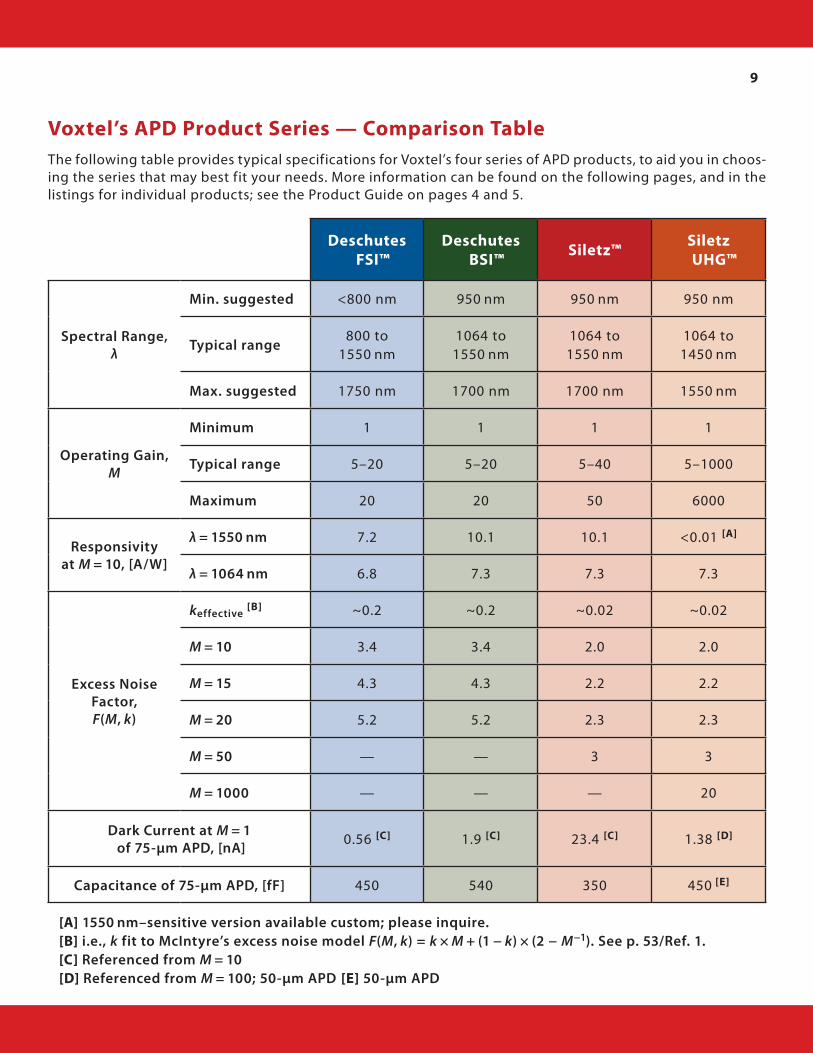
Voxtel’s APD Product Series — Comparison Table
Deschutes FSI™
Deschutes BSI™ Siletz™ Siletz
UHG™
Spectral Range, λ
Min suggested <800 nm 950 nm 950 nm 950 nm
Typical range800 to
1550 nm1064 to
1550 nm1064 to
1550 nm1064 to
1450 nm
Max suggested 1750 nm 1700 nm 1700 nm 1550 nm
Operating Gain, M
Minimum 1 1 1 1
Typical range 5–20 5–20 5–40 5–1000
Maximum 20 20 50 6000
Responsivity at M = 10, [A/W]
λ = 1550 nm 7.2 10.1 10.1 <0.01 [A]
λ = 1064 nm 6.8 7.3 7.3 7.3
Excess Noise Factor, F(M, k)
keffective [B] ~0.2 ~0.2 ~0.02 ~0.02
M = 10 3.4 3.4 2.0 2.0
M = 15 4.3 4.3 2.2 2.2
M = 20 5.2 5.2 2.3 2.3
M = 50 — — 3 3
M = 1000 — — — 20
Dark Current at M = 1 of 75-µm APD, [nA] 0.56 [C] 1.9 [C] 23.4 [C] 1.38 [D]
Capacitance of 75-µm APD, [fF] 450 540 350 450 [E]
[A] 1550 nm–sensitive version available custom; please inquire [B] i e , k fit to McIntyre’s excess noise model F(M, k) = k × M + (1 − k) × (2 − M−1) See p 53/Ref 1 [C] Referenced from M = 10[D] Referenced from M = 100; 50-µm APD [E] 50-µm APD
The following table provides typical specifications for Voxtel’s four series of APD products, to aid you in choos-ing the series that may best fit your needs. More information can be found on the following pages, and in the listings for individual products; see the Product Guide on pages 4 and 5.
Comparison Table
10
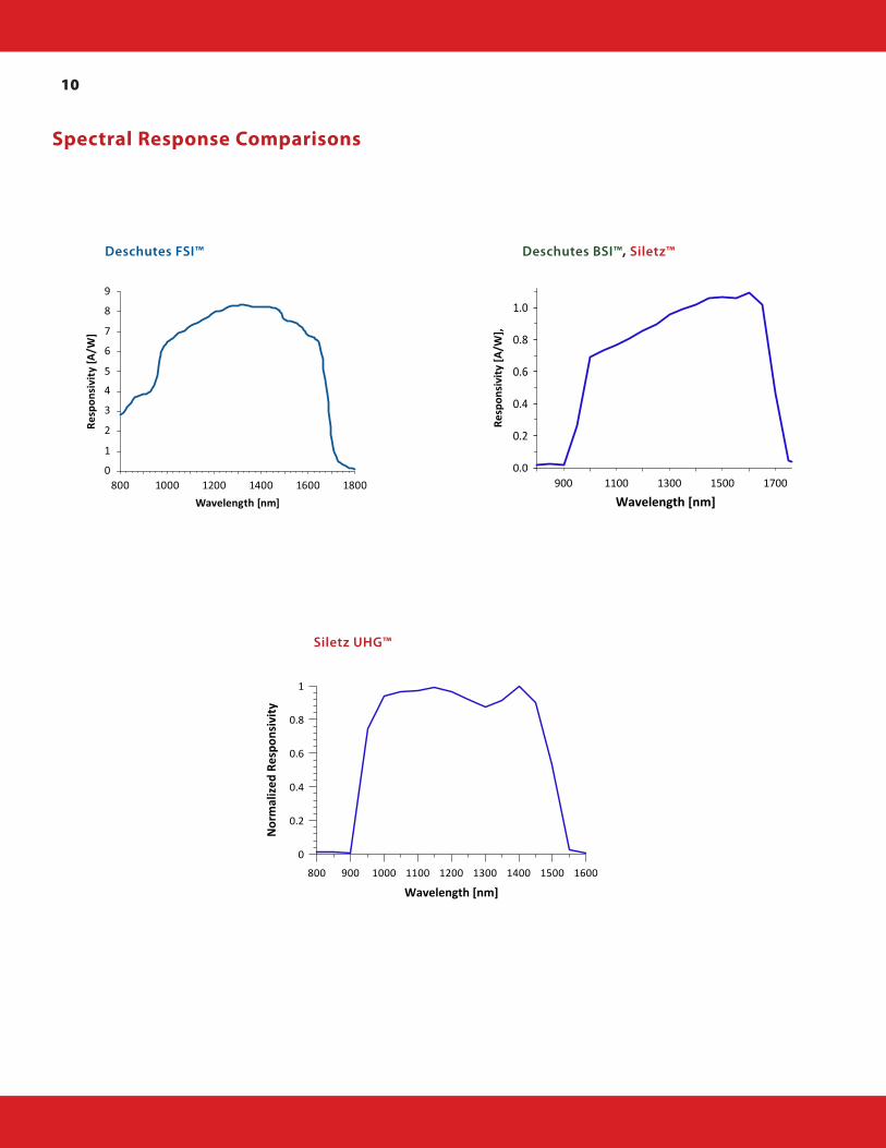
Spectral Response Comparisons
Siletz UHG™
Deschutes FSI™ Deschutes BSI™, Siletz™
800 900 1000 1100 1200 1300 1400 1500 1600
1
0.8
0.6
0.4
0.2
0
Wavelength [nm]
Nor
mal
ized
Res
pons
ivit
y
0
1
2
3
4
5
6
7
8
9
800 1000 1200 1400 1600 1800
Wavelength [nm]
Resp
onsi
vity
[A/W
]
0.0
0.2
0.4
0.6
0.8
1.0
900 1100 1300 1500 1700
Wavelength [nm]Re
spon
sivi
ty [A
/W],
11
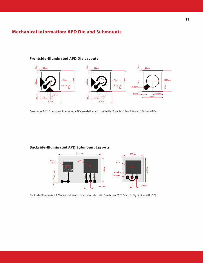
Backside-Illuminated APD Submount Layouts
Mechanical Information: APD Die and Submounts
Frontside-Illuminated APD Die Layouts
Deschutes FSI™ frontside-illuminated APDs are delivered as bare die. From left: 30-, 75-, and 200-µm APDs.
Backside-illuminated APDs are delivered on submounts. Left: Deschutes BSI™, Siletz™. Right: Siletz-UHG™) .
735 µm
860 µm
150 μm
APD
Anode
Cathode
25 μm
80 μ
m
175 μm 113 μm
350 μm
Ø 28 μm
Ø 75 μm
175
μm
350
μm
25 μ
m16
0 μm
25 μm
80 μ
m
175 μm 113 μm
350 μm
Ø 76 μm
Ø 75 μm
175
μm
350
μm
25 μ
m16
0 μm
25 μm
65 μm
65 μ
m
175 μm
350 μm
Ø 200 μm
Anode Ø 75 μm
175
μm
350
μm
25 μ
m
E EBC
1.52 mm
940 µm
Temp.Sense
150 μm
APD
100 μm
E EBC
Ano
de
Cath
ode
Cath
ode
12
Deschutes FSI™Avalanche Photodiodes
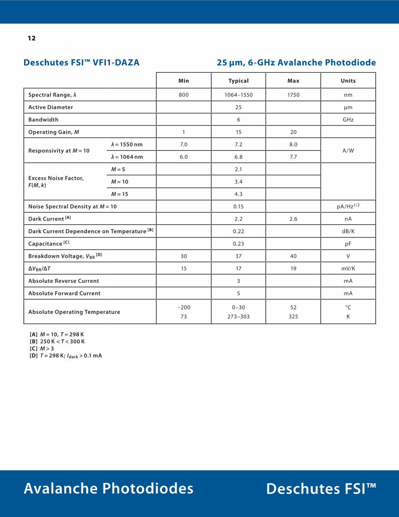
Deschutes FSI™ VFI1-DAZA 25 µm, 6-GHz Avalanche Photodiode
Min Typical Max Units
Spectral Range, λ 800 1064–1550 1750 nm
Active Diameter 25 µm
Bandwidth 6 GHz
Operating Gain, M 1 15 20
Responsivity at M = 10λ = 1550 nm 7.0 7.2 8.0
A/Wλ = 1064 nm 6.0 6.8 7.7
Excess Noise Factor, F(M, k)
M = 5 2.1
M = 10 3.4
M = 15 4.3
Noise Spectral Density at M = 10 0.15 pA/Hz1/2
Dark Current [A] 2.2 2.6 nA
Dark Current Dependence on Temperature [B] 0.22 dB/K
Capacitance [C] 0.23 pF
Breakdown Voltage, VBR [D] 30 37 40 V
ΔVBR/ΔT 15 17 19 mV/K
Absolute Reverse Current 3 mA
Absolute Forward Current 5 mA
Absolute Operating Temperature−200
73
0–30
273–303
52
325
°C
K
[A] M = 10, T = 298 K [B] 250 K < T < 300 K [C] M > 3 [D] T = 298 K; Idark > 0 1 mA
APD Product Listings Avalanche Photodiodes

13
Deschutes FSI™Avalanche Photodiodes
Deschutes FSI™ VFI1-JAZA 75 µm, 2-GHz Avalanche Photodiode
Min Typical Max Units
Spectral Range, λ 800 1064–1550 1750 nm
Active Diameter 75 µm
Bandwidth 2 GHz
Operating Gain, M 1 15 20
Responsivity at M = 10λ = 1550 nm 7.0 7.2 8.0
A/Wλ = 1064 nm 6.0 6.8 7.7
Excess Noise Factor, F(M, k)
M = 5 2.1
M = 10 3.4
M = 15 4.3
Noise Spectral Density at M = 10 0.25 pA/Hz1/2
Dark Current [A] 5.6 7 nA
Dark Current Dependence on Temperature [B] 0.24 dB/K
Capacitance [C] 0.45 pF
Breakdown Voltage, VBR [D] 30 37 40 V
ΔVBR/ΔT 15 17 19 mV/K
Absolute Reverse Current 3 mA
Absolute Forward Current 5 mA
Absolute Operating Temperature−200
73
0–30
273–303
52
325
°C
K
[A] M = 10, T = 298 K [B] 250 K < T < 300 K [C] M > 3 [D] T = 294 K; Idark > 0 1 mA
14
Deschutes FSI™Avalanche Photodiodes
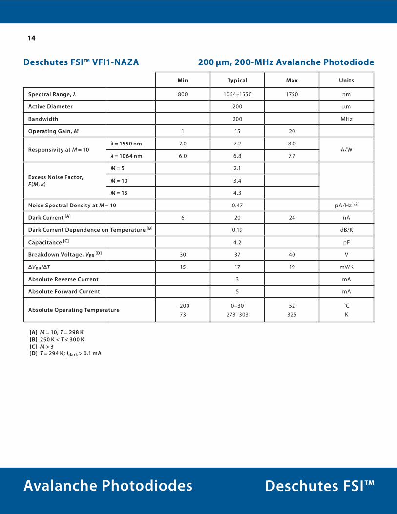
Deschutes FSI™ VFI1-NAZA 200 µm, 200-MHz Avalanche Photodiode
Min Typical Max Units
Spectral Range, λ 800 1064–1550 1750 nm
Active Diameter 200 µm
Bandwidth 200 MHz
Operating Gain, M 1 15 20
Responsivity at M = 10λ = 1550 nm 7.0 7.2 8.0
A/Wλ = 1064 nm 6.0 6.8 7.7
Excess Noise Factor, F(M, k)
M = 5 2.1
M = 10 3.4
M = 15 4.3
Noise Spectral Density at M = 10 0.47 pA/Hz1/2
Dark Current [A] 6 20 24 nA
Dark Current Dependence on Temperature [B] 0.19 dB/K
Capacitance [C] 4.2 pF
Breakdown Voltage, VBR [D] 30 37 40 V
ΔVBR/ΔT 15 17 19 mV/K
Absolute Reverse Current 3 mA
Absolute Forward Current 5 mA
Absolute Operating Temperature−200
73
0–30
273–303
52
325
°C
K
[A] M = 10, T = 298 K [B] 250 K < T < 300 K [C] M > 3 [D] T = 294 K; Idark > 0 1 mA
15
Deschutes BSI™Avalanche Photodiodes
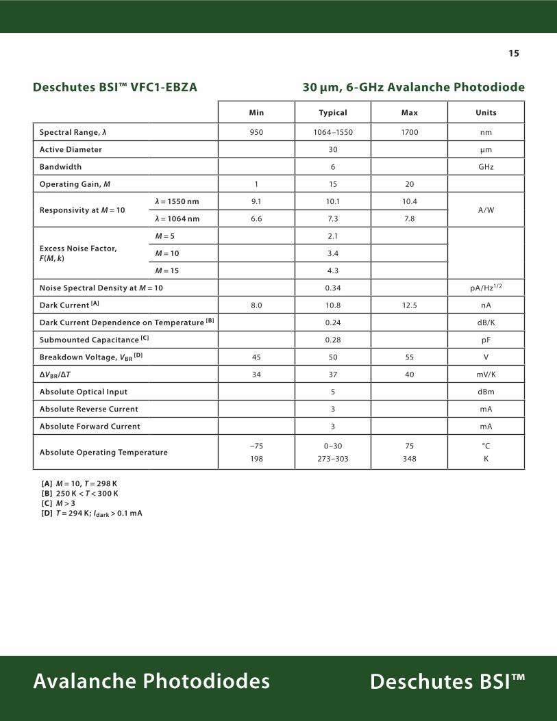
Deschutes BSI™ VFC1-EBZA 30 µm, 6-GHz Avalanche Photodiode
Min Typical Max Units
Spectral Range, λ 950 1064–1550 1700 nm
Active Diameter 30 µm
Bandwidth 6 GHz
Operating Gain, M 1 15 20
Responsivity at M = 10λ = 1550 nm 9.1 10.1 10.4
A/Wλ = 1064 nm 6.6 7.3 7.8
Excess Noise Factor, F(M, k)
M = 5 2.1
M = 10 3.4
M = 15 4.3
Noise Spectral Density at M = 10 0.34 pA/Hz1/2
Dark Current [A] 8.0 10.8 12.5 nA
Dark Current Dependence on Temperature [B] 0.24 dB/K
Submounted Capacitance [C] 0.28 pF
Breakdown Voltage, VBR [D] 45 50 55 V
ΔVBR/ΔT 34 37 40 mV/K
Absolute Optical Input 5 dBm
Absolute Reverse Current 3 mA
Absolute Forward Current 3 mA
Absolute Operating Temperature−75
198
0–30
273–303
75
348
°C
K
[A] M = 10, T = 298 K [B] 250 K < T < 300 K [C] M > 3 [D] T = 294 K; Idark > 0 1 mA
16
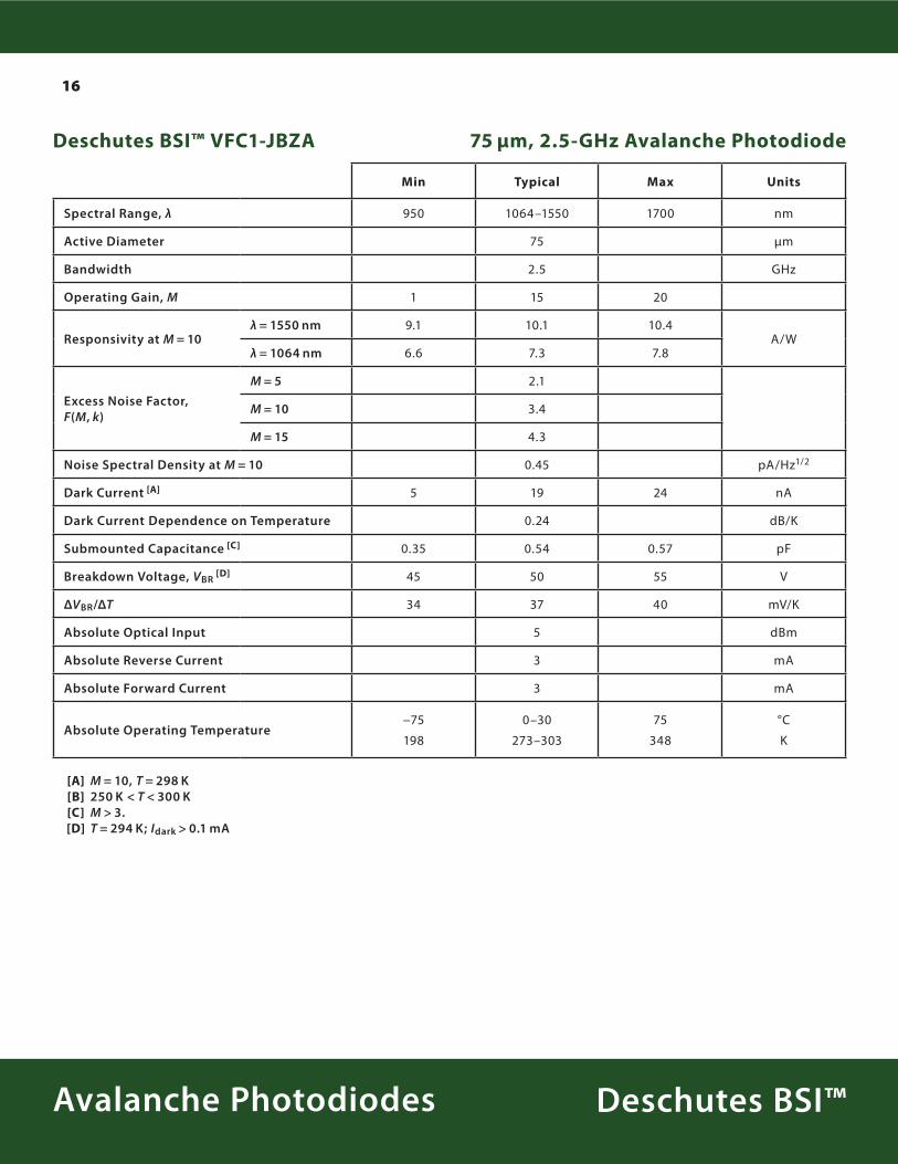
Deschutes BSI™Avalanche Photodiodes
Deschutes BSI™ VFC1-JBZA 75 µm, 2.5-GHz Avalanche Photodiode
Min Typical Max Units
Spectral Range, λ 950 1064–1550 1700 nm
Active Diameter 75 µm
Bandwidth 2.5 GHz
Operating Gain, M 1 15 20
Responsivity at M = 10λ = 1550 nm 9.1 10.1 10.4
A/Wλ = 1064 nm 6.6 7.3 7.8
Excess Noise Factor, F(M, k)
M = 5 2.1
M = 10 3.4
M = 15 4.3
Noise Spectral Density at M = 10 0.45 pA/Hz1/2
Dark Current [A] 5 19 24 nA
Dark Current Dependence on Temperature 0.24 dB/K
Submounted Capacitance [C] 0.35 0.54 0.57 pF
Breakdown Voltage, VBR [D] 45 50 55 V
ΔVBR/ΔT 34 37 40 mV/K
Absolute Optical Input 5 dBm
Absolute Reverse Current 3 mA
Absolute Forward Current 3 mA
Absolute Operating Temperature−75
198
0–30
273–303
75
348
°C
K
[A] M = 10, T = 298 K [B] 250 K < T < 300 K [C] M > 3 [D] T = 294 K; Idark > 0 1 mA
17
Deschutes BSI™Avalanche Photodiodes
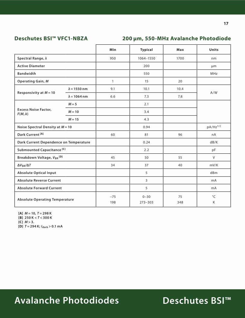
Deschutes BSI™ VFC1-NBZA 200 µm, 550-MHz Avalanche Photodiode
Min Typical Max Units
Spectral Range, λ 950 1064–1550 1700 nm
Active Diameter 200 µm
Bandwidth 550 MHz
Operating Gain, M 1 15 20
Responsivity at M = 10λ = 1550 nm 9.1 10.1 10.4
A/Wλ = 1064 nm 6.6 7.3 7.8
Excess Noise Factor, F(M, k)
M = 5 2.1
M = 10 3.4
M = 15 4.3
Noise Spectral Density at M = 10 0.94 pA/Hz1/2
Dark Current [A] 60 81 96 nA
Dark Current Dependence on Temperature 0.24 dB/K
Submounted Capacitance [C] 2.2 pF
Breakdown Voltage, VBR [D] 45 50 55 V
ΔVBR/ΔT 34 37 40 mV/K
Absolute Optical Input 5 dBm
Absolute Reverse Current 3 mA
Absolute Forward Current 5 mA
Absolute Operating Temperature−75
198
0–30
273–303
75
348
°C
K
[A] M = 10, T = 298 K [B] 250 K < T < 300 K [C] M > 3 [D] T = 294 K; Idark > 0 1 mA

18
Siletz™Avalanche Photodiodes
Siletz™ VFP1-EBZA 30 µm, 2.3-GHz Avalanche Photodiode
Min Typical Max Units
Spectral Range, λ 950 1064–1550 1700 nm
Active Diameter 30 µm
Bandwidth 2.3 GHz
Operating Gain, M 1 5–40 50
Responsivity at M = 10λ = 1550 nm 9.1 10.1 10.4
A/Wλ = 1064 nm 6.6 7.3 7.8
Excess Noise Factor, F(M, k)
keffective [A] <0.02
M = 10 2.0
M = 20 2.3
M = 50 2.9
Noise Spectral Density at M = 10 0.43 pA/Hz1/2
Dark Current at M = 1 [B] 6.6 nA
Dark Current Dependence on Temperature [C] 0.11 dB/K
Submounted Capacitance 60 fF
Breakdown Voltage, VBR [D] 70 74 80 V
ΔVBR/ΔT 29 mV/K
[A] i e , k fit to McIntyre’s excess noise model F(M, k) = k × M + (1 − k) × (2 − M−1) See p 53/Ref 1 [B] Referenced from M = 10 [C] 250 K < T < 300 K [D] T = 294 K; Idark > 0 1 mA
19
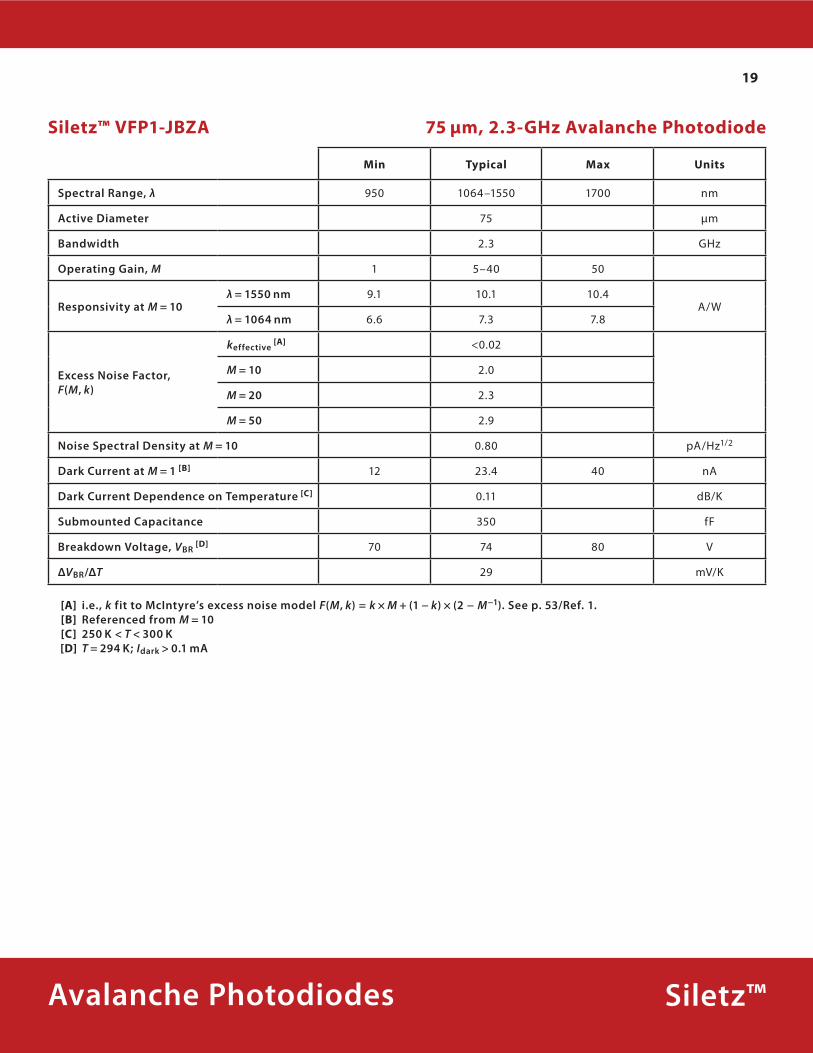
Siletz™Avalanche Photodiodes
Siletz™ VFP1-JBZA 75 µm, 2.3-GHz Avalanche Photodiode
Min Typical Max Units
Spectral Range, λ 950 1064–1550 1700 nm
Active Diameter 75 µm
Bandwidth 2.3 GHz
Operating Gain, M 1 5–40 50
Responsivity at M = 10λ = 1550 nm 9.1 10.1 10.4
A/Wλ = 1064 nm 6.6 7.3 7.8
Excess Noise Factor, F(M, k)
keffective [A] <0.02
M = 10 2.0
M = 20 2.3
M = 50 2.9
Noise Spectral Density at M = 10 0.80 pA/Hz1/2
Dark Current at M = 1 [B] 12 23.4 40 nA
Dark Current Dependence on Temperature [C] 0.11 dB/K
Submounted Capacitance 350 fF
Breakdown Voltage, VBR [D] 70 74 80 V
ΔVBR/ΔT 29 mV/K
[A] i e , k fit to McIntyre’s excess noise model F(M, k) = k × M + (1 − k) × (2 − M−1) See p 53/Ref 1 [B] Referenced from M = 10 [C] 250 K < T < 300 K [D] T = 294 K; Idark > 0 1 mA
20
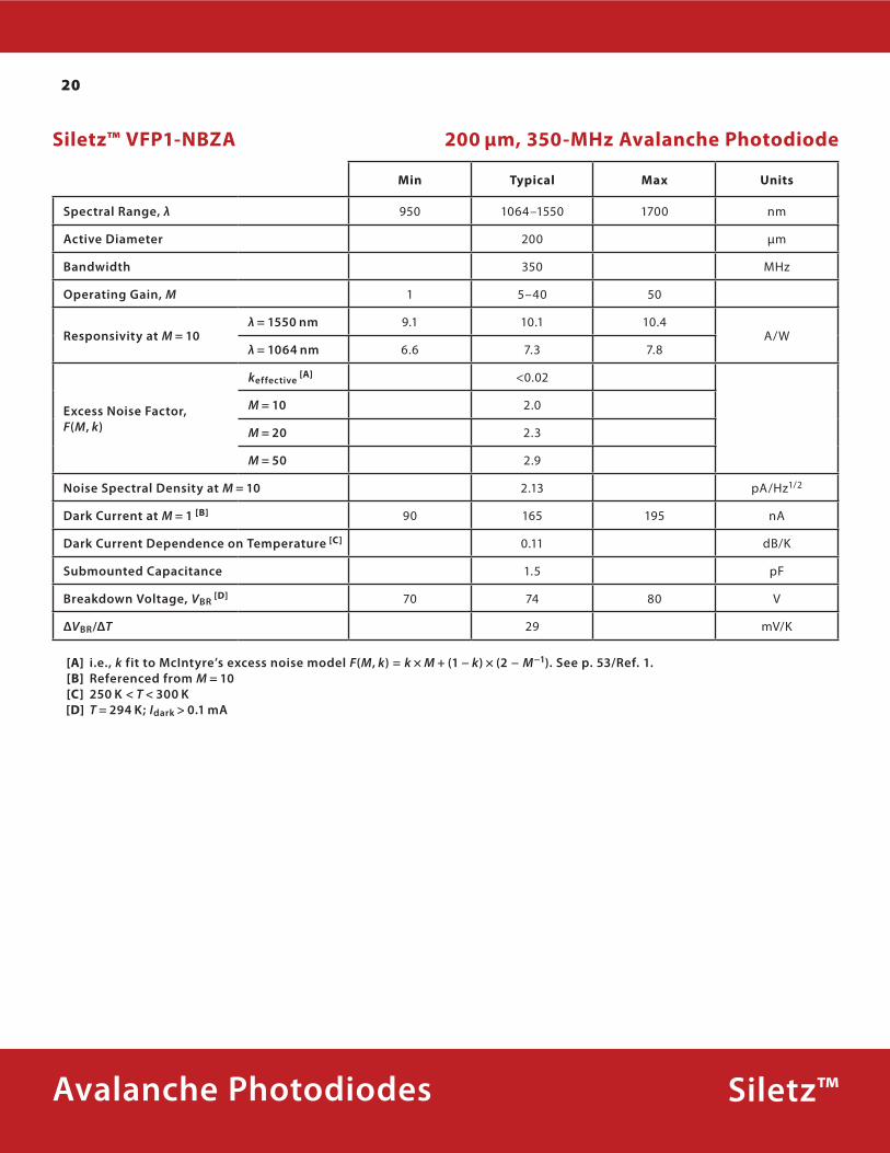
Siletz™Avalanche Photodiodes
Siletz™ VFP1-NBZA 200 µm, 350-MHz Avalanche Photodiode
Min Typical Max Units
Spectral Range, λ 950 1064–1550 1700 nm
Active Diameter 200 µm
Bandwidth 350 MHz
Operating Gain, M 1 5–40 50
Responsivity at M = 10λ = 1550 nm 9.1 10.1 10.4
A/Wλ = 1064 nm 6.6 7.3 7.8
Excess Noise Factor, F(M, k)
keffective [A] <0.02
M = 10 2.0
M = 20 2.3
M = 50 2.9
Noise Spectral Density at M = 10 2.13 pA/Hz1/2
Dark Current at M = 1 [B] 90 165 195 nA
Dark Current Dependence on Temperature [C] 0.11 dB/K
Submounted Capacitance 1.5 pF
Breakdown Voltage, VBR [D] 70 74 80 V
ΔVBR/ΔT 29 mV/K
[A] i e , k fit to McIntyre’s excess noise model F(M, k) = k × M + (1 − k) × (2 − M−1) See p 53/Ref 1 [B] Referenced from M = 10 [C] 250 K < T < 300 K [D] T = 294 K; Idark > 0 1 mA
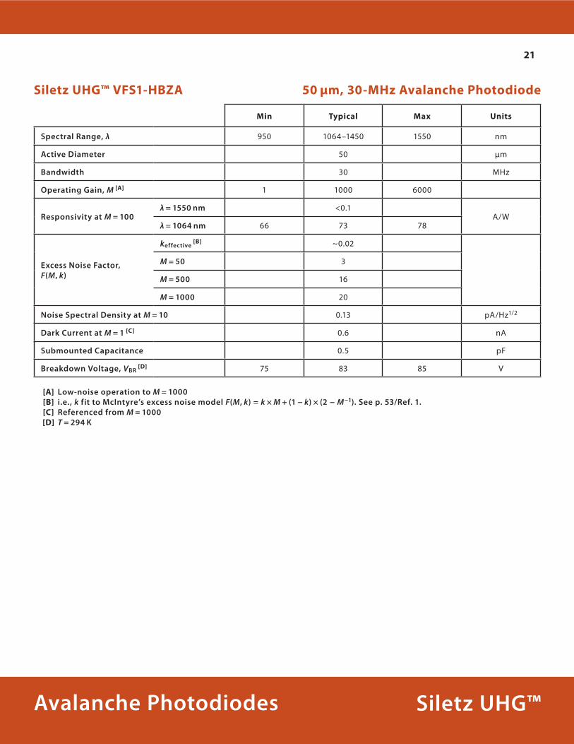
21
Siletz UHG™Avalanche Photodiodes
Siletz UHG™ VFS1-HBZA 50 µm, 30-MHz Avalanche Photodiode
Min Typical Max Units
Spectral Range, λ 950 1064–1450 1550 nm
Active Diameter 50 µm
Bandwidth 30 MHz
Operating Gain, M [A] 1 1000 6000
Responsivity at M = 100λ = 1550 nm <0.1
A/Wλ = 1064 nm 66 73 78
Excess Noise Factor, F(M, k)
keffective [B] ~0.02
M = 50 3
M = 500 16
M = 1000 20
Noise Spectral Density at M = 10 0.13 pA/Hz1/2
Dark Current at M = 1 [C] 0.6 nA
Submounted Capacitance 0.5 pF
Breakdown Voltage, VBR [D] 75 83 85 V
[A] Low-noise operation to M = 1000 [B] i e , k fit to McIntyre’s excess noise model F(M, k) = k × M + (1 − k) × (2 − M−1) See p 53/Ref 1 [C] Referenced from M = 1000 [D] T = 294 K
22
Siletz UHG™Avalanche Photodiodes
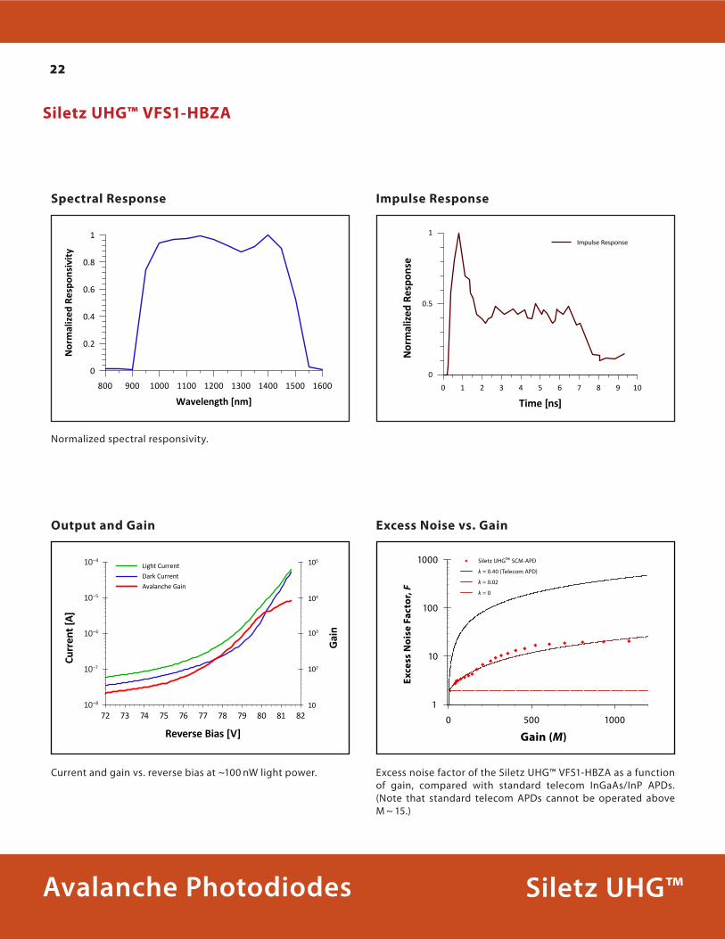
Output and Gain Excess Noise vs. Gain
Excess noise factor of the Siletz UHG™ VFS1-HBZA as a function of gain, compared with standard telecom InGaAs/InP APDs. (Note that standard telecom APDs cannot be operated above M ~ 15.)
72 73 74 75 76 77 78 79 80 81 82
105
104
103
102
10
Light Current
Dark Current
Avalanche Gain
Reverse Bias [V]
Curr
ent [
A]
Gai
n
10–4
10–5
10–6
10–7
10–8
0 500 1000
1
1000
100
10
Exce
ss N
oise
Fac
tor,
F
Gain (M)
k = 0
k = 0.40 (Telecom APD)
k = 0.02
Siletz UHG™ SCM-APD
Current and gain vs. reverse bias at ~100 nW light power.
Impulse Response
0 1 2 3 4 5 6 7 8 9 10
1
0.5
0
Impulse Response
Time [ns]N
orm
aliz
ed R
espo
nse
Spectral Response
800 900 1000 1100 1200 1300 1400 1500 1600
1
0.8
0.6
0.4
0.2
0
Wavelength [nm]
Nor
mal
ized
Res
pons
ivit
y
Normalized spectral responsivity.
Siletz UHG™ VFS1-HBZA
23
Mechanical Information: Packaged APDs
TO-46 Package
TO-8 Package
Pinout 1) TEC – 4) TEC + 9) Temp Sense – 10) Temp Sense + 11) APD Anode (P) 12) APD Cathode (N)
Ø 15.24
5.72
2.87
1.91
9.53
Ø 0.460.79
0.79 1 4
12 11 10 9
25.40 ± 0.64
9.91
7.16 mm
5.38
2.24 ± 0.31
APD Plane
Active area Ø 1.52
Pinout1) APD Cathode2) APD Anode3) Ground, T Sense –4) T Sense +
SIDE VIEWwith cap
TOP VIEWheader only
Ø .019Ø .016
Ø .171Ø .161
Ø .100
.700
.500
.043
.031
.045
.037
Ø .026Ø .020
.072 in183 mm
Ø .212Ø .209
Ø .048Ø .046.010
.007
.006
.000
45° ± 0.5°
.118
.114
.012
.009
.046
.042
.010 max.
1
2
3
4
Packaged APDs
24
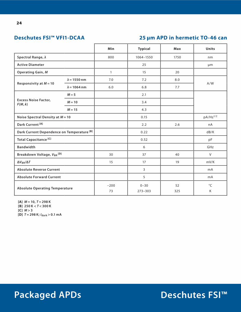
Deschutes FSI™Packaged APDs
Deschutes FSI™ VFI1-DCAA 25 µm APD in hermetic TO-46 can
Min Typical Max Units
Spectral Range, λ 800 1064–1550 1750 nm
Active Diameter 25 µm
Operating Gain, M 1 15 20
Responsivity at M = 10λ = 1550 nm 7.0 7.2 8.0
A/Wλ = 1064 nm 6.0 6.8 7.7
Excess Noise Factor, F(M, k)
M = 5 2.1
M = 10 3.4
M = 15 4.3
Noise Spectral Density at M = 10 0.15 pA/Hz1/2
Dark Current [A] 2.2 2.6 nA
Dark Current Dependence on Temperature [B] 0.22 dB/K
Total Capacitance [C] 0.52 pF
Bandwidth 6 GHz
Breakdown Voltage, VBR [D] 30 37 40 V
ΔVBR/ΔT 15 17 19 mV/K
Absolute Reverse Current 3 mA
Absolute Forward Current 5 mA
Absolute Operating Temperature−200
73
0–30
273–303
52
325
°C
K
[A] M = 10, T = 298 K [B] 250 K < T < 300 K [C] M > 3 [D] T = 298 K; Idark > 0 1 mA
25
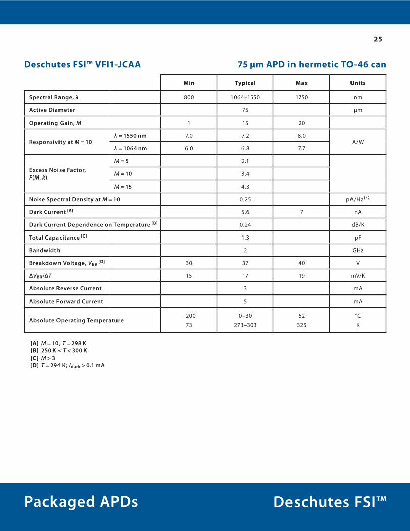
Deschutes FSI™Packaged APDs
Deschutes FSI™ VFI1-JCAA 75 µm APD in hermetic TO-46 can
Min Typical Max Units
Spectral Range, λ 800 1064–1550 1750 nm
Active Diameter 75 µm
Operating Gain, M 1 15 20
Responsivity at M = 10λ = 1550 nm 7.0 7.2 8.0
A/Wλ = 1064 nm 6.0 6.8 7.7
Excess Noise Factor, F(M, k)
M = 5 2.1
M = 10 3.4
M = 15 4.3
Noise Spectral Density at M = 10 0.25 pA/Hz1/2
Dark Current [A] 5.6 7 nA
Dark Current Dependence on Temperature [B] 0.24 dB/K
Total Capacitance [C] 1.3 pF
Bandwidth 2 GHz
Breakdown Voltage, VBR [D] 30 37 40 V
ΔVBR/ΔT 15 17 19 mV/K
Absolute Reverse Current 3 mA
Absolute Forward Current 5 mA
Absolute Operating Temperature−200
73
0–30
273–303
52
325
°C
K
[A] M = 10, T = 298 K [B] 250 K < T < 300 K [C] M > 3 [D] T = 294 K; Idark > 0 1 mA
26
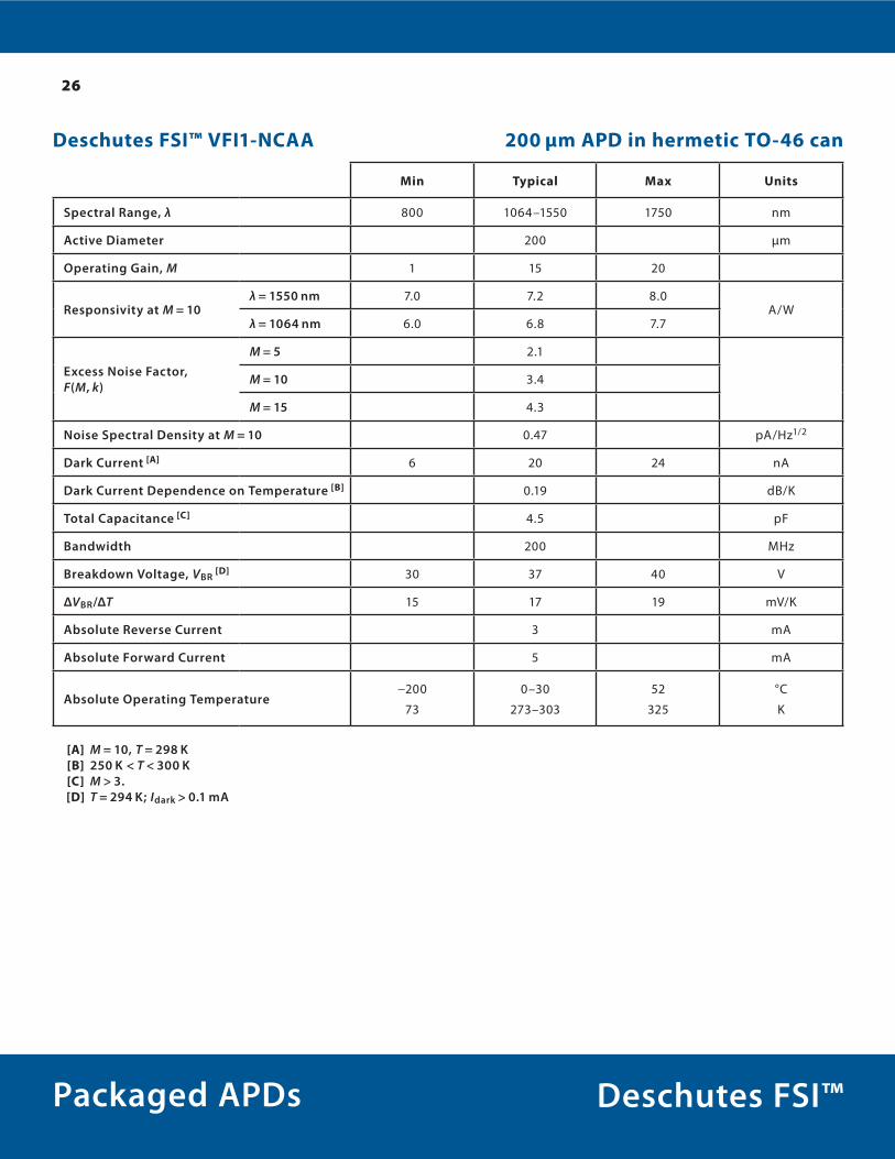
Deschutes FSI™Packaged APDs
Deschutes FSI™ VFI1-NCAA 200 µm APD in hermetic TO-46 can
Min Typical Max Units
Spectral Range, λ 800 1064–1550 1750 nm
Active Diameter 200 µm
Operating Gain, M 1 15 20
Responsivity at M = 10λ = 1550 nm 7.0 7.2 8.0
A/Wλ = 1064 nm 6.0 6.8 7.7
Excess Noise Factor, F(M, k)
M = 5 2.1
M = 10 3.4
M = 15 4.3
Noise Spectral Density at M = 10 0.47 pA/Hz1/2
Dark Current [A] 6 20 24 nA
Dark Current Dependence on Temperature [B] 0.19 dB/K
Total Capacitance [C] 4.5 pF
Bandwidth 200 MHz
Breakdown Voltage, VBR [D] 30 37 40 V
ΔVBR/ΔT 15 17 19 mV/K
Absolute Reverse Current 3 mA
Absolute Forward Current 5 mA
Absolute Operating Temperature−200
73
0–30
273–303
52
325
°C
K
[A] M = 10, T = 298 K [B] 250 K < T < 300 K [C] M > 3 [D] T = 294 K; Idark > 0 1 mA
27
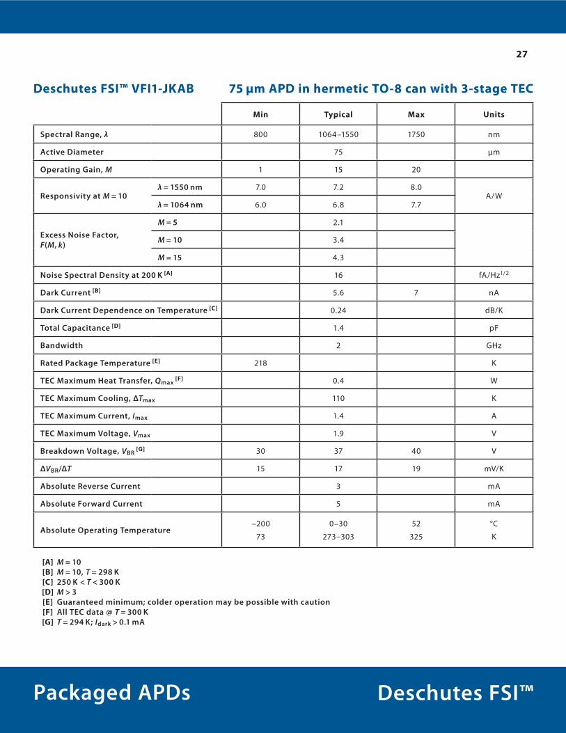
Deschutes FSI™Packaged APDs
Deschutes FSI™ VFI1-JKAB 75 µm APD in hermetic TO-8 can with 3-stage TEC
Min Typical Max Units
Spectral Range, λ 800 1064–1550 1750 nm
Active Diameter 75 µm
Operating Gain, M 1 15 20
Responsivity at M = 10λ = 1550 nm 7.0 7.2 8.0
A/Wλ = 1064 nm 6.0 6.8 7.7
Excess Noise Factor, F(M, k)
M = 5 2.1
M = 10 3.4
M = 15 4.3
Noise Spectral Density at 200 K [A] 16 fA/Hz1/2
Dark Current [B] 5.6 7 nA
Dark Current Dependence on Temperature [C] 0.24 dB/K
Total Capacitance [D] 1.4 pF
Bandwidth 2 GHz
Rated Package Temperature [E] 218 K
TEC Maximum Heat Transfer, Qmax [F] 0.4 W
TEC Maximum Cooling, ΔTmax 110 K
TEC Maximum Current, Imax 1.4 A
TEC Maximum Voltage, Vmax 1.9 V
Breakdown Voltage, VBR [G] 30 37 40 V
ΔVBR/ΔT 15 17 19 mV/K
Absolute Reverse Current 3 mA
Absolute Forward Current 5 mA
Absolute Operating Temperature−200
73
0–30
273–303
52
325
°C
K
[A] M = 10 [B] M = 10, T = 298 K [C] 250 K < T < 300 K [D] M > 3 [E] Guaranteed minimum; colder operation may be possible with caution [F] All TEC data @ T = 300 K [G] T = 294 K; Idark > 0 1 mA
28
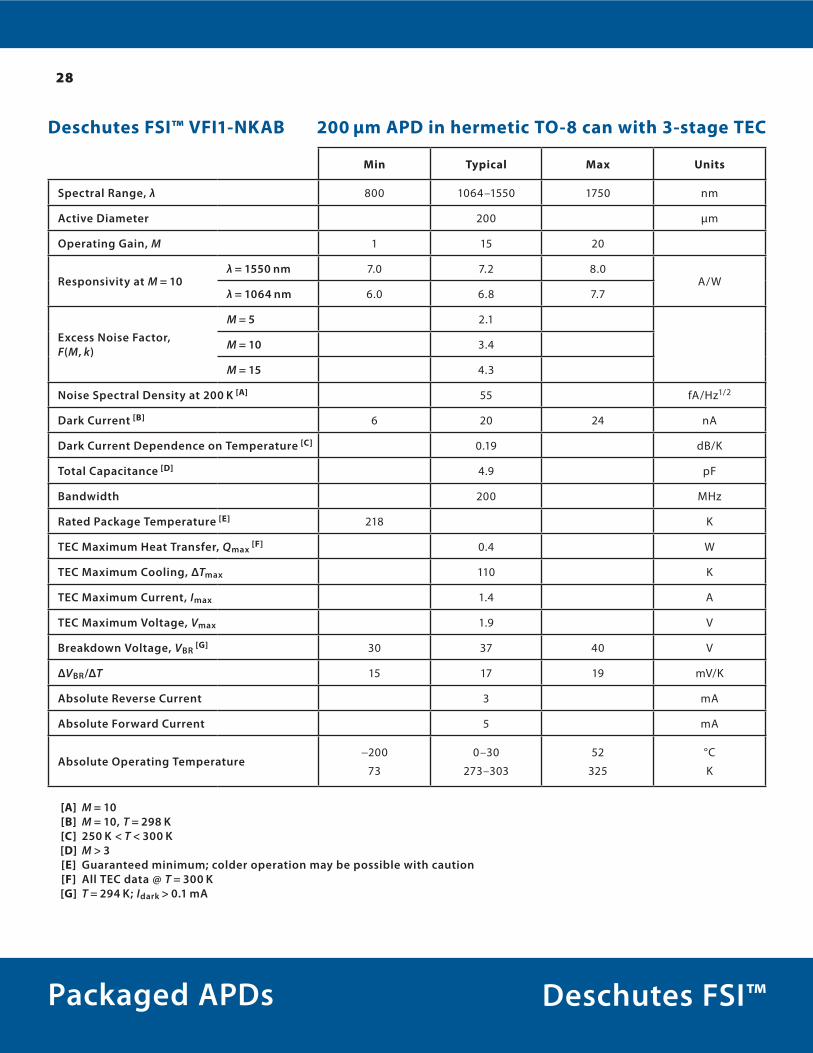
Deschutes FSI™Packaged APDs
Deschutes FSI™ VFI1-NKAB 200 µm APD in hermetic TO-8 can with 3-stage TEC
Min Typical Max Units
Spectral Range, λ 800 1064–1550 1750 nm
Active Diameter 200 µm
Operating Gain, M 1 15 20
Responsivity at M = 10λ = 1550 nm 7.0 7.2 8.0
A/Wλ = 1064 nm 6.0 6.8 7.7
Excess Noise Factor, F(M, k)
M = 5 2.1
M = 10 3.4
M = 15 4.3
Noise Spectral Density at 200 K [A] 55 fA/Hz1/2
Dark Current [B] 6 20 24 nA
Dark Current Dependence on Temperature [C] 0.19 dB/K
Total Capacitance [D] 4.9 pF
Bandwidth 200 MHz
Rated Package Temperature [E] 218 K
TEC Maximum Heat Transfer, Qmax [F] 0.4 W
TEC Maximum Cooling, ΔTmax 110 K
TEC Maximum Current, Imax 1.4 A
TEC Maximum Voltage, Vmax 1.9 V
Breakdown Voltage, VBR [G] 30 37 40 V
ΔVBR/ΔT 15 17 19 mV/K
Absolute Reverse Current 3 mA
Absolute Forward Current 5 mA
Absolute Operating Temperature−200
73
0–30
273–303
52
325
°C
K
[A] M = 10 [B] M = 10, T = 298 K [C] 250 K < T < 300 K [D] M > 3 [E] Guaranteed minimum; colder operation may be possible with caution [F] All TEC data @ T = 300 K [G] T = 294 K; Idark > 0 1 mA
29
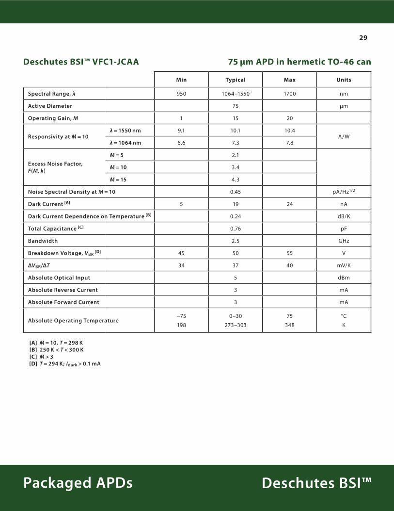
Deschutes BSI™Packaged APDs
Deschutes BSI™ VFC1-JCAA 75 µm APD in hermetic TO-46 can
Min Typical Max Units
Spectral Range, λ 950 1064–1550 1700 nm
Active Diameter 75 µm
Operating Gain, M 1 15 20
Responsivity at M = 10λ = 1550 nm 9.1 10.1 10.4
A/Wλ = 1064 nm 6.6 7.3 7.8
Excess Noise Factor, F(M, k)
M = 5 2.1
M = 10 3.4
M = 15 4.3
Noise Spectral Density at M = 10 0.45 pA/Hz1/2
Dark Current [A] 5 19 24 nA
Dark Current Dependence on Temperature [B] 0.24 dB/K
Total Capacitance [C] 0.76 pF
Bandwidth 2.5 GHz
Breakdown Voltage, VBR [D] 45 50 55 V
ΔVBR/ΔT 34 37 40 mV/K
Absolute Optical Input 5 dBm
Absolute Reverse Current 3 mA
Absolute Forward Current 3 mA
Absolute Operating Temperature−75
198
0–30
273–303
75
348
°C
K
[A] M = 10, T = 298 K [B] 250 K < T < 300 K [C] M > 3 [D] T = 294 K; Idark > 0 1 mA
30
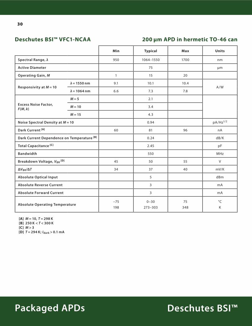
Deschutes BSI™Packaged APDs
Deschutes BSI™ VFC1-NCAA 200 µm APD in hermetic TO-46 can
Min Typical Max Units
Spectral Range, λ 950 1064–1550 1700 nm
Active Diameter 75 µm
Operating Gain, M 1 15 20
Responsivity at M = 10λ = 1550 nm 9.1 10.1 10.4
A/Wλ = 1064 nm 6.6 7.3 7.8
Excess Noise Factor, F(M, k)
M = 5 2.1
M = 10 3.4
M = 15 4.3
Noise Spectral Density at M = 10 0.94 pA/Hz1/2
Dark Current [A] 60 81 96 nA
Dark Current Dependence on Temperature [B] 0.24 dB/K
Total Capacitance [C] 2.45 pF
Bandwidth 550 MHz
Breakdown Voltage, VBR [D] 45 50 55 V
ΔVBR/ΔT 34 37 40 mV/K
Absolute Optical Input 5 dBm
Absolute Reverse Current 3 mA
Absolute Forward Current 3 mA
Absolute Operating Temperature−75
198
0–30
273–303
75
348
°C
K
[A] M = 10, T = 298 K [B] 250 K < T < 300 K [C] M > 3 [D] T = 294 K; Idark > 0 1 mA
31
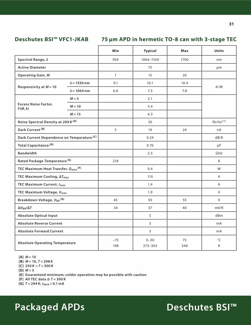
Deschutes BSI™Packaged APDs
Deschutes BSI™ VFC1-JKAB 75 µm APD in hermetic TO-8 can with 3-stage TEC
Min Typical Max Units
Spectral Range, λ 950 1064–1550 1700 nm
Active Diameter 75 µm
Operating Gain, M 1 15 20
Responsivity at M = 10λ = 1550 nm 9.1 10.1 10.4
A/Wλ = 1064 nm 6.6 7.3 7.8
Excess Noise Factor, F(M, k)
M = 5 2.1
M = 10 3.4
M = 15 4.3
Noise Spectral Density at 200 K [A] 30 fA/Hz1/2
Dark Current [B] 5 19 24 nA
Dark Current Dependence on Temperature [C] 0.24 dB/K
Total Capacitance [D] 0.76 pF
Bandwidth 2.5 GHz
Rated Package Temperature [E] 218 K
TEC Maximum Heat Transfer, Qmax [F] 0.4 W
TEC Maximum Cooling, ΔTmax 110 K
TEC Maximum Current, Imax 1.4 A
TEC Maximum Voltage, Vmax 1.9 V
Breakdown Voltage, VBR [G] 45 50 55 V
ΔVBR/ΔT 34 37 40 mV/K
Absolute Optical Input 5 dBm
Absolute Reverse Current 3 mA
Absolute Forward Current 3 mA
Absolute Operating Temperature−75
198
0–30
273–303
75
348
°C
K
[A] M = 10 [B] M = 10, T = 298 K [C] 250 K < T < 300 K [D] M > 3 [E] Guaranteed minimum; colder operation may be possible with caution [F] All TEC data @ T = 300 K [G] T = 294 K; Idark > 0 1 mA
32
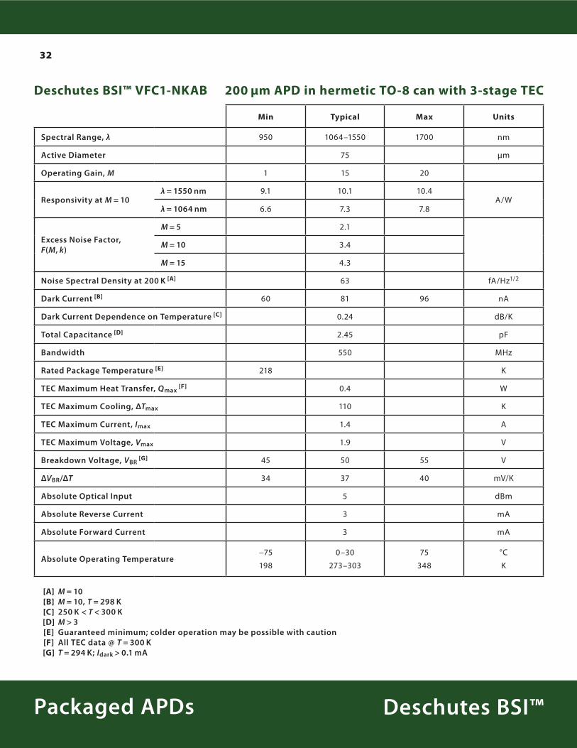
Deschutes BSI™Packaged APDs
Deschutes BSI™ VFC1-NKAB 200 µm APD in hermetic TO-8 can with 3-stage TEC
Min Typical Max Units
Spectral Range, λ 950 1064–1550 1700 nm
Active Diameter 75 µm
Operating Gain, M 1 15 20
Responsivity at M = 10λ = 1550 nm 9.1 10.1 10.4
A/Wλ = 1064 nm 6.6 7.3 7.8
Excess Noise Factor, F(M, k)
M = 5 2.1
M = 10 3.4
M = 15 4.3
Noise Spectral Density at 200 K [A] 63 fA/Hz1/2
Dark Current [B] 60 81 96 nA
Dark Current Dependence on Temperature [C] 0.24 dB/K
Total Capacitance [D] 2.45 pF
Bandwidth 550 MHz
Rated Package Temperature [E] 218 K
TEC Maximum Heat Transfer, Qmax [F] 0.4 W
TEC Maximum Cooling, ΔTmax 110 K
TEC Maximum Current, Imax 1.4 A
TEC Maximum Voltage, Vmax 1.9 V
Breakdown Voltage, VBR [G] 45 50 55 V
ΔVBR/ΔT 34 37 40 mV/K
Absolute Optical Input 5 dBm
Absolute Reverse Current 3 mA
Absolute Forward Current 3 mA
Absolute Operating Temperature−75
198
0–30
273–303
75
348
°C
K
[A] M = 10 [B] M = 10, T = 298 K [C] 250 K < T < 300 K [D] M > 3 [E] Guaranteed minimum; colder operation may be possible with caution [F] All TEC data @ T = 300 K [G] T = 294 K; Idark > 0 1 mA
33
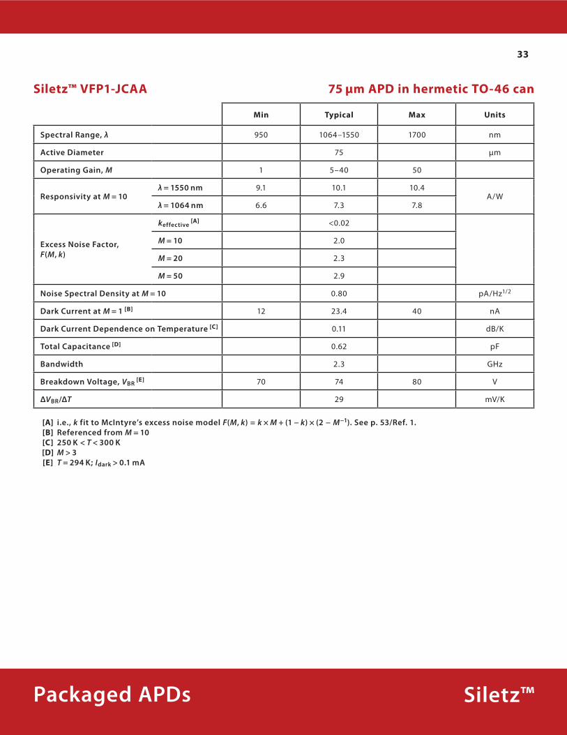
Siletz™Packaged APDs
Siletz™ VFP1-JCAA 75 µm APD in hermetic TO-46 can
Min Typical Max Units
Spectral Range, λ 950 1064–1550 1700 nm
Active Diameter 75 µm
Operating Gain, M 1 5–40 50
Responsivity at M = 10λ = 1550 nm 9.1 10.1 10.4
A/Wλ = 1064 nm 6.6 7.3 7.8
Excess Noise Factor, F(M, k)
keffective [A] <0.02
M = 10 2.0
M = 20 2.3
M = 50 2.9
Noise Spectral Density at M = 10 0.80 pA/Hz1/2
Dark Current at M = 1 [B] 12 23.4 40 nA
Dark Current Dependence on Temperature [C] 0.11 dB/K
Total Capacitance [D] 0.62 pF
Bandwidth 2.3 GHz
Breakdown Voltage, VBR [E] 70 74 80 V
ΔVBR/ΔT 29 mV/K
[A] i e , k fit to McIntyre’s excess noise model F(M, k) = k × M + (1 − k) × (2 − M−1) See p 53/Ref 1 [B] Referenced from M = 10 [C] 250 K < T < 300 K [D] M > 3 [E] T = 294 K; Idark > 0 1 mA

34
Siletz™Packaged APDs
Siletz™ VFP1-NCAA 200 µm APD in hermetic TO-46 can
Min Typical Max Units
Spectral Range, λ 950 1064–1550 1700 nm
Active Diameter 200 µm
Operating Gain, M 1 5–40 50
Responsivity at M = 10λ = 1550 nm 9.1 10.1 10.4
A/Wλ = 1064 nm 6.6 7.3 7.8
Excess Noise Factor, F(M, k)
keffective [A] <0.02
M = 10 2.0
M = 20 2.3
M = 50 2.9
Noise Spectral Density at M = 10 2.13 pA/Hz1/2
Dark Current at M = 1 [B] 90 165 195 nA
Total Capacitance [C] 1.86 pF
Bandwidth 350 MHz
Breakdown Voltage, VBR [D] 70 74 80 V
ΔVBR/ΔT 29 mV/K
[A] i e , k fit to McIntyre’s excess noise model F(M, k) = k × M + (1 − k) × (2 − M−1) See p 53/Ref 1 [B] Referenced from M = 10 [C] M > 3 [D] T = 294 K; Idark > 0 1 mA
35
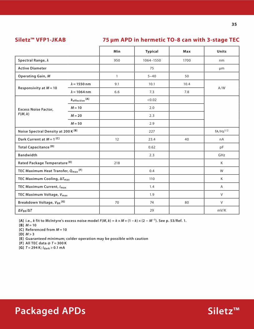
Siletz™Packaged APDs
Siletz™ VFP1-JKAB 75 µm APD in hermetic TO-8 can with 3-stage TEC
Min Typical Max Units
Spectral Range, λ 950 1064–1550 1700 nm
Active Diameter 75 µm
Operating Gain, M 1 5–40 50
Responsivity at M = 10λ = 1550 nm 9.1 10.1 10.4
A/Wλ = 1064 nm 6.6 7.3 7.8
Excess Noise Factor, F(M, k)
keffective [A] <0.02
M = 10 2.0
M = 20 2.3
M = 50 2.9
Noise Spectral Density at 200 K [B] 227 fA/Hz1/2
Dark Current at M = 1 [C] 12 23.4 40 nA
Total Capacitance [D] 0.62 pF
Bandwidth 2.3 GHz
Rated Package Temperature [E] 218 K
TEC Maximum Heat Transfer, Qmax [F] 0.4 W
TEC Maximum Cooling, ΔTmax 110 K
TEC Maximum Current, Imax 1.4 A
TEC Maximum Voltage, Vmax 1.9 V
Breakdown Voltage, VBR [G] 70 74 80 V
ΔVBR/ΔT 29 mV/K
[A] i e , k fit to McIntyre’s excess noise model F(M, k) = k × M + (1 − k) × (2 − M−1) See p 53/Ref 1 [B] M = 10 [C] Referenced from M = 10 [D] M > 3 [E] Guaranteed minimum; colder operation may be possible with caution [F] All TEC data @ T = 300 K [G] T = 294 K; Idark > 0 1 mA
36
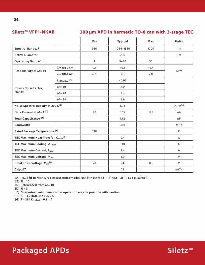
Siletz™Packaged APDs
Siletz™ VFP1-NKAB 200 µm APD in hermetic TO-8 can with 3-stage TEC
Min Typical Max Units
Spectral Range, λ 950 1064–1550 1700 nm
Active Diameter 200 µm
Operating Gain, M 1 5–40 50
Responsivity at M = 10λ = 1550 nm 9.1 10.1 10.4
A/Wλ = 1064 nm 6.6 7.3 7.8
Excess Noise Factor, F(M, k)
keffective [A] <0.02
M = 10 2.0
M = 20 2.3
M = 50 2.9
Noise Spectral Density at 200 K [B] 603 fA/Hz1/2
Dark Current at M = 1 [C] 90 165 195 nA
Total Capacitance [D] 1.86 pF
Bandwidth 350 MHz
Rated Package Temperature [E] 218 K
TEC Maximum Heat Transfer, Qmax [F] 0.4 W
TEC Maximum Cooling, ΔTmax 110 K
TEC Maximum Current, Imax 1.4 A
TEC Maximum Voltage, Vmax 1.9 V
Breakdown Voltage, VBR [G] 70 74 80 V
ΔVBR/ΔT 29 mV/K
[A] i e , k fit to McIntyre’s excess noise model F(M, k) = k × M + (1 − k) × (2 − M−1) See p 53/Ref 1 [B] M = 10 [C] Referenced from M = 10 [D] M > 3 [E] Guaranteed minimum; colder operation may be possible with caution [F] All TEC data @ T = 300 K [G] T = 294 K; Idark > 0 1 mA
37
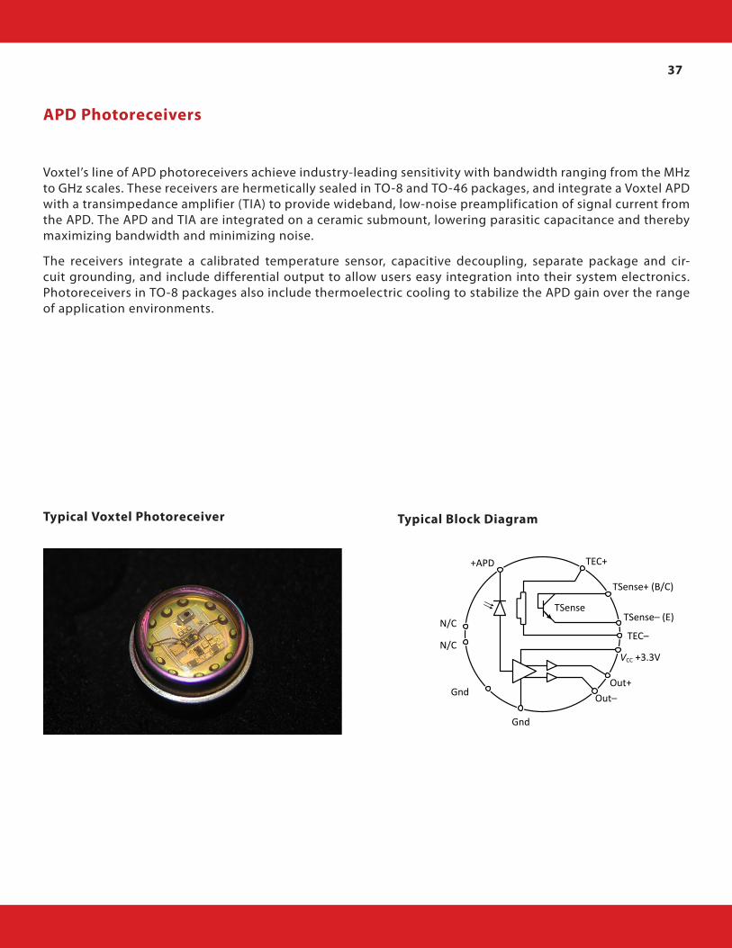
APD Photoreceivers
Typical Voxtel Photoreceiver Typical Block Diagram
Voxtel’s line of APD photoreceivers achieve industry-leading sensitivity with bandwidth ranging from the MHz to GHz scales. These receivers are hermetically sealed in TO-8 and TO-46 packages, and integrate a Voxtel APD with a transimpedance amplifier (TIA) to provide wideband, low-noise preamplification of signal current from the APD. The APD and TIA are integrated on a ceramic submount, lowering parasitic capacitance and thereby maximizing bandwidth and minimizing noise.
The receivers integrate a calibrated temperature sensor, capacitive decoupling, separate package and cir-cuit grounding, and include differential output to allow users easy integration into their system electronics. Photoreceivers in TO-8 packages also include thermoelectric cooling to stabilize the APD gain over the range of application environments.
TSense+ (B/C)
TSense– (E)
VCC +3.3V
TEC–
TEC++APD
Gnd
Gnd
N/C
Out+
Out–
N/C
TSense
38
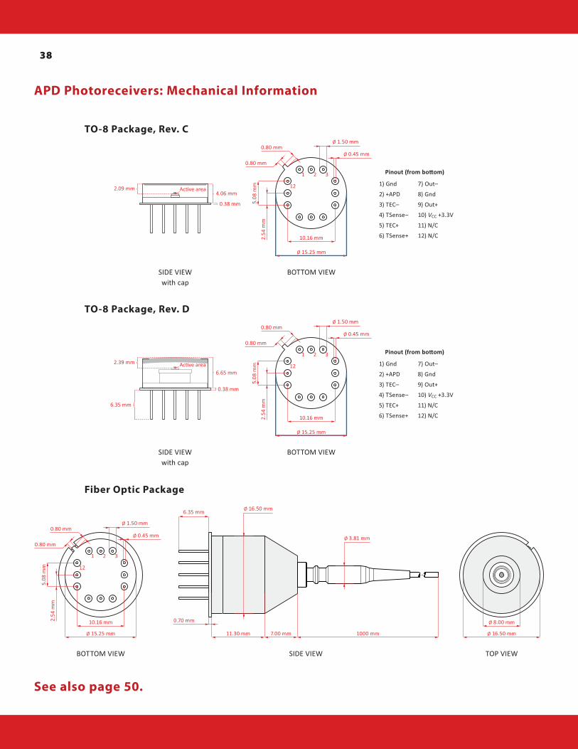
APD Photoreceivers: Mechanical Information
TO-8 Package, Rev. C
TO-8 Package, Rev. D
Fiber Optic Package
Ø 15.25 mm
10.16 mm
Ø 0.45 mm
Ø 1.50 mm
1) Gnd
2) +APD
3) TEC–
4) TSense–
5) TEC+
6) TSense+
Pinout (from boom)
7) Out–
8) Gnd
9) Out+
10) VCC +3.3V
11) N/C
12) N/C
0.80 mm
5.08
mm
2.54
mm
0.80 mm
1 2 3
122.09 mm Acve area4.06 mm
0.38 mm
SIDE VIEWwith cap
BOTTOM VIEW
Ø 15.25 mm
10.16 mm
Ø 0.45 mm
Ø 1.50 mm
1) Gnd
2) +APD
3) TEC–
4) TSense–
5) TEC+
6) TSense+
Pinout (from boom)
7) Out–
8) Gnd
9) Out+
10) VCC +3.3V
11) N/C
12) N/C
0.80 mm
5.08
mm
2.54
mm
0.80 mm
1 2 3
12
SIDE VIEWwith cap
BOTTOM VIEW
2.39 mm
6.65 mm
0.38 mm
6.35 mm
Acve area
1 2 3
12
10.16 mm
Ø 15.25 mm
Ø 0.45 mm
Ø 1.50 mm
0.80 mm
5.08
mm
2.54
mm
0.80 mm
Ø 16.50 mm
Ø 8.00 mm
11.30 mm 7.00 mm 1000 mm
0.70 mm
6.35 mm
Ø 3.81 mm
Ø 16.50 mm
BOTTOM VIEW TOP VIEWSIDE VIEW
See also page 50.

39
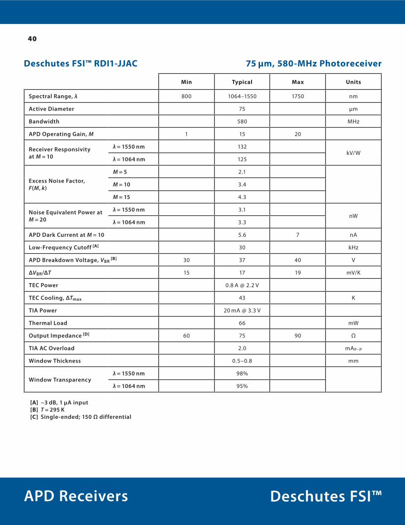
Deschutes FSI™APD Receivers
Deschutes FSI™ RDI1-NJAC 200 µm, 200-MHz Photoreceiver
Min Typical Max Units
Spectral Range, λ 800 1064–1550 1750 nm
Active Diameter 200 µm
Bandwidth 200 MHz
APD Operating Gain, M 1 15 20
Receiver Responsivity at M = 10
λ = 1550 nm 132kV/W
λ = 1064 nm 125
Excess Noise Factor, F(M, k)
M = 5 2.1
M = 10 3.4
M = 15 4.3
Noise Equivalent Power at M = 20
λ = 1550 nm 3.1nW
λ = 1064 nm 3.3
APD Dark Current at M = 10 6 20 24 nA
Low-Frequency Cutoff [A] 30 kHz
APD Breakdown Voltage, VBR [B] 30 37 40 V
ΔVBR/ΔT 15 17 19 mV/K
TEC Power 0.8 A @ 2.2 V
TEC Cooling, ΔTmax 43 K
TIA Power 20 mA @ 3.3 V
Thermal Load 66 mW
Output Impedance [C] 60 75 90 Ω
TIA AC Overload 2.0 mAP–P
Window Thickness 0.5–0.8 mm
Window Transparencyλ = 1550 nm 98%
λ = 1064 nm 95%
[A] −3 dB, 1 µA input [B] T = 295 K [C] Single-ended; 150 Ω differential
40
Deschutes FSI™APD Receivers
Deschutes FSI™ RDI1-JJAC 75 µm, 580-MHz Photoreceiver
Min Typical Max Units
Spectral Range, λ 800 1064–1550 1750 nm
Active Diameter 75 µm
Bandwidth 580 MHz
APD Operating Gain, M 1 15 20
Receiver Responsivity at M = 10
λ = 1550 nm 132kV/W
λ = 1064 nm 125
Excess Noise Factor, F(M, k)
M = 5 2.1
M = 10 3.4
M = 15 4.3
Noise Equivalent Power at M = 20
λ = 1550 nm 3.1nW
λ = 1064 nm 3.3
APD Dark Current at M = 10 5.6 7 nA
Low-Frequency Cutoff [A] 30 kHz
APD Breakdown Voltage, VBR [B] 30 37 40 V
ΔVBR/ΔT 15 17 19 mV/K
TEC Power 0.8 A @ 2.2 V
TEC Cooling, ΔTmax 43 K
TIA Power 20 mA @ 3.3 V
Thermal Load 66 mW
Output Impedance [D] 60 75 90 Ω
TIA AC Overload 2.0 mAP–P
Window Thickness 0.5–0.8 mm
Window Transparencyλ = 1550 nm 98%
λ = 1064 nm 95%
[A] −3 dB, 1 µA input [B] T = 295 K [C] Single-ended; 150 Ω differential
41
Deschutes BSI™APD Receivers
Deschutes BSI™ RJC1-NJAC 200 µm, 200-MHz Photoreceiver
Min Typical Max Units
Spectral Range, λ 950 1064–1550 1700 nm
Active Diameter 200 µm
Bandwidth 200 MHz
APD Operating Gain, M 1 15 20
Receiver Responsivity at M = 20
λ = 1550 nm 372kV/W
λ = 1064 nm 228
Excess Noise Factor, F(M, k)
M = 5 2.1
M = 10 3.4
M = 15 4.3
Noise Equivalent Power at M = 20
λ = 1550 nm 1.8nW
λ = 1064 nm 2.3
APD Dark Current at M = 10 60 81 96 nA
Low-Frequency Cutoff [A] 30 kHz
APD Breakdown Voltage, VBR [B] 45 50 55 V
ΔVBR/ΔT 34 37 40 mV/K
TEC Power 0.8 A @ 2.2 V
TEC Cooling, ΔTmax 43 K
TIA Power 20 mA @ 3.3 V
Thermal Load 66 mW
Output Impedance [D] 60 75 90 Ω
TIA AC Overload 2.0 mAP–P
Window Thickness 0.5–0.8 mm
Window Transparencyλ = 1550 nm 98%
λ = 1064 nm 95%
Temperature Sensor Sensitivity 2.18 mV/K
[A] −3 dB, 1 µA input [C] at T = 298 K [B] T = 295 K [D] Single-ended; 150 Ω differential
See also page 43.
42
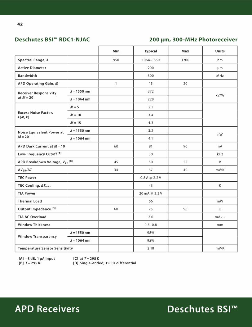
Deschutes BSI™APD Receivers
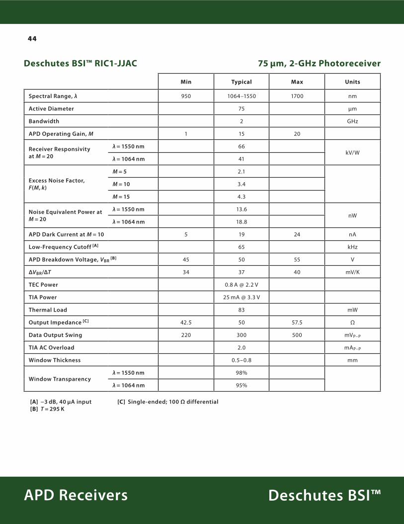
Deschutes BSI™ RDC1-NJAC 200 µm, 300-MHz Photoreceiver
Min Typical Max Units
Spectral Range, λ 950 1064–1550 1700 nm
Active Diameter 200 µm
Bandwidth 300 MHz
APD Operating Gain, M 1 15 20
Receiver Responsivity at M = 20
λ = 1550 nm 372kV/W
λ = 1064 nm 228
Excess Noise Factor, F(M, k)
M = 5 2.1
M = 10 3.4
M = 15 4.3
Noise Equivalent Power at M = 20
λ = 1550 nm 3.2nW
λ = 1064 nm 4.1
APD Dark Current at M = 10 60 81 96 nA
Low-Frequency Cutoff [A] 30 kHz
APD Breakdown Voltage, VBR [B] 45 50 55 V
ΔVBR/ΔT 34 37 40 mV/K
TEC Power 0.8 A @ 2.2 V
TEC Cooling, ΔTmax 43 K
TIA Power 20 mA @ 3.3 V
Thermal Load 66 mW
Output Impedance [D] 60 75 90 Ω
TIA AC Overload 2.0 mAP–P
Window Thickness 0.5–0.8 mm
Window Transparencyλ = 1550 nm 98%
λ = 1064 nm 95%
Temperature Sensor Sensitivity 2.18 mV/K
[A] −3 dB, 1 µA input [C] at T = 298 K [B] T = 295 K [D] Single-ended; 150 Ω differential
43
Deschutes BSI™APD Receivers
Deschutes BSI™ RJC1-NJAC
Deschutes BSI™ RDC1-NJAC
250
200
150
100
50
0
0.1 0.30.2 0.5 1 32
Signal Power [µW]
Resp
onsi
vity
[kV/
W] Avg.
95%90%
Avg.95%90%M=10
M=20
Linearity of Response
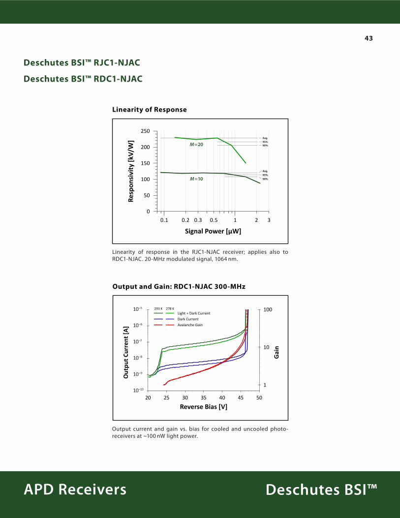
Linearity of response in the RJC1-NJAC receiver; applies also to RDC1-NJAC. 20-MHz modulated signal, 1064 nm.
20 25 30 35 40 45 50
100
10
1
Light + Dark Current
Dark Current
Avalanche Gain
Reverse Bias [V]
Out
put C
urre
nt [A
]
Gai
n
10–5
10–6
10–7
10–8
10–9
10–10
278 K293 K
Output and Gain: RDC1-NJAC 300-MHz
Output current and gain vs. bias for cooled and uncooled photo-receivers at ~100 nW light power.
44
Deschutes BSI™APD Receivers
Deschutes BSI™ RIC1-JJAC 75 µm, 2-GHz Photoreceiver
Min Typical Max Units
Spectral Range, λ 950 1064–1550 1700 nm
Active Diameter 75 µm
Bandwidth 2 GHz
APD Operating Gain, M 1 15 20
Receiver Responsivity at M = 20
λ = 1550 nm 66kV/W
λ = 1064 nm 41
Excess Noise Factor, F(M, k)
M = 5 2.1
M = 10 3.4
M = 15 4.3
Noise Equivalent Power at M = 20
λ = 1550 nm 13.6nW
λ = 1064 nm 18.8
APD Dark Current at M = 10 5 19 24 nA
Low-Frequency Cutoff [A] 65 kHz
APD Breakdown Voltage, VBR [B] 45 50 55 V
ΔVBR/ΔT 34 37 40 mV/K
TEC Power 0.8 A @ 2.2 V
TIA Power 25 mA @ 3.3 V
Thermal Load 83 mW
Output Impedance [C] 42.5 50 57.5 Ω
Data Output Swing 220 300 500 mVP–P
TIA AC Overload 2.0 mAP–P
Window Thickness 0.5–0.8 mm
Window Transparencyλ = 1550 nm 98%
λ = 1064 nm 95%
[A] −3 dB, 40 µA input [C] Single-ended; 100 Ω differential [B] T = 295 K
45
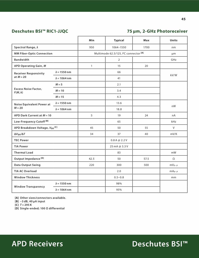
Deschutes BSI™APD Receivers
Deschutes BSI™ RIC1-JJQC 75 µm, 2-GHz Photoreceiver
Min Typical Max Units
Spectral Range, λ 950 1064–1550 1700 nm
MM Fiber-Optic Connection Multimode 62.5/125, FC connector [A] µm
Bandwidth 2 GHz
APD Operating Gain, M 1 15 20
Receiver Responsivity at M = 20
λ = 1550 nm 66kV/W
λ = 1064 nm 41
Excess Noise Factor, F(M, k)
M = 5 2.1
M = 10 3.4
M = 15 4.3
Noise Equivalent Power at M = 20
λ = 1550 nm 13.6nW
λ = 1064 nm 18.8
APD Dark Current at M = 10 5 19 24 nA
Low-Frequency Cutoff [B] 65 kHz
APD Breakdown Voltage, VBR [C] 45 50 55 V
ΔVBR/ΔT 34 37 40 mV/K
TEC Power 0.8 A @ 2.2 V
TIA Power 25 mA @ 3.3 V
Thermal Load 83 mW
Output Impedance [D] 42.5 50 57.5 Ω
Data Output Swing 220 300 500 mVP–P
TIA AC Overload 2.0 mAP–P
Window Thickness 0.5–0.8 mm
Window Transparencyλ = 1550 nm 98%
λ = 1064 nm 95%
[A] Other sizes/connectors available [B] −3 dB, 40 µA input [C] T = 295 K [D] Single-ended; 100 Ω differential
46
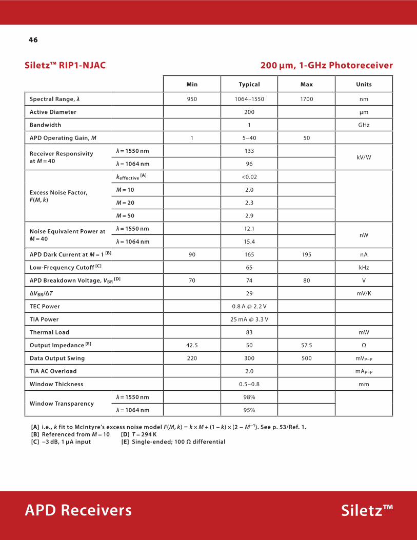
Siletz™APD Receivers
Min Typical Max Units
Spectral Range, λ 950 1064–1550 1700 nm
Active Diameter 200 µm
Bandwidth 1 GHz
APD Operating Gain, M 1 5–40 50
Receiver Responsivity at M = 40
λ = 1550 nm 133kV/W
λ = 1064 nm 96
Excess Noise Factor, F(M, k)
keffective [A] <0.02
M = 10 2.0
M = 20 2.3
M = 50 2.9
Noise Equivalent Power at M = 40
λ = 1550 nm 12.1nW
λ = 1064 nm 15.4
APD Dark Current at M = 1 [B] 90 165 195 nA
Low-Frequency Cutoff [C] 65 kHz
APD Breakdown Voltage, VBR [D] 70 74 80 V
ΔVBR/ΔT 29 mV/K
TEC Power 0.8 A @ 2.2 V
TIA Power 25 mA @ 3.3 V
Thermal Load 83 mW
Output Impedance [E] 42.5 50 57.5 Ω
Data Output Swing 220 300 500 mVP–P
TIA AC Overload 2.0 mAP–P
Window Thickness 0.5–0.8 mm
Window Transparencyλ = 1550 nm 98%
λ = 1064 nm 95%
[A] i e , k fit to McIntyre’s excess noise model F(M, k) = k × M + (1 − k) × (2 − M−1) See p 53/Ref 1 [B] Referenced from M = 10 [D] T = 294 K [C] −3 dB, 1 µA input [E] Single-ended; 100 Ω differential
Siletz™ RIP1-NJAC 200 µm, 1-GHz Photoreceiver
47
Siletz™APD Receivers
Min Typical Max Units
Spectral Range, λ 950 1064–1550 1700 nm
Active Diameter 75 µm
Bandwidth 2.1 GHz
APD Operating Gain, M 1 5–40 50
Receiver Responsivity at M = 40
λ = 1550 nm 133kV/W
λ = 1064 nm 96
Excess Noise Factor, F(M, k)
keffective [A] <0.02
M = 10 2.0
M = 20 2.3
M = 50 2.9
Noise Equivalent Power at M = 40
λ = 1550 nm 8.2nW
λ = 1064 nm 10.5
APD Dark Current at M = 1 [B] 12 23.4 40 nA
Low-Frequency Cutoff [C] 65 kHz
APD Breakdown Voltage, VBR [D] 70 74 80 V
ΔVBR/ΔT 29 mV/K
TEC Power 0.8 A @ 2.2 V
TIA Power 25 mA @ 3.3 V
Thermal Load 83 mW
Output Impedance [E] 42.5 50 57.5 Ω
Data Output Swing 220 300 500 mVP–P
TIA AC Overload 2.0 mAP–P
Window Thickness 0.5–0.8 mm
Window Transparencyλ = 1550 nm 98%
λ = 1064 nm 95%
[A] i e , k fit to McIntyre’s excess noise model F(M, k) = k × M + (1 − k) × (2 − M−1) See p 53/Ref 1 [B] Referenced from M = 10 [D] T = 294 K [C] −3 dB, 1 µA input [E] Single-ended; 100 Ω differential
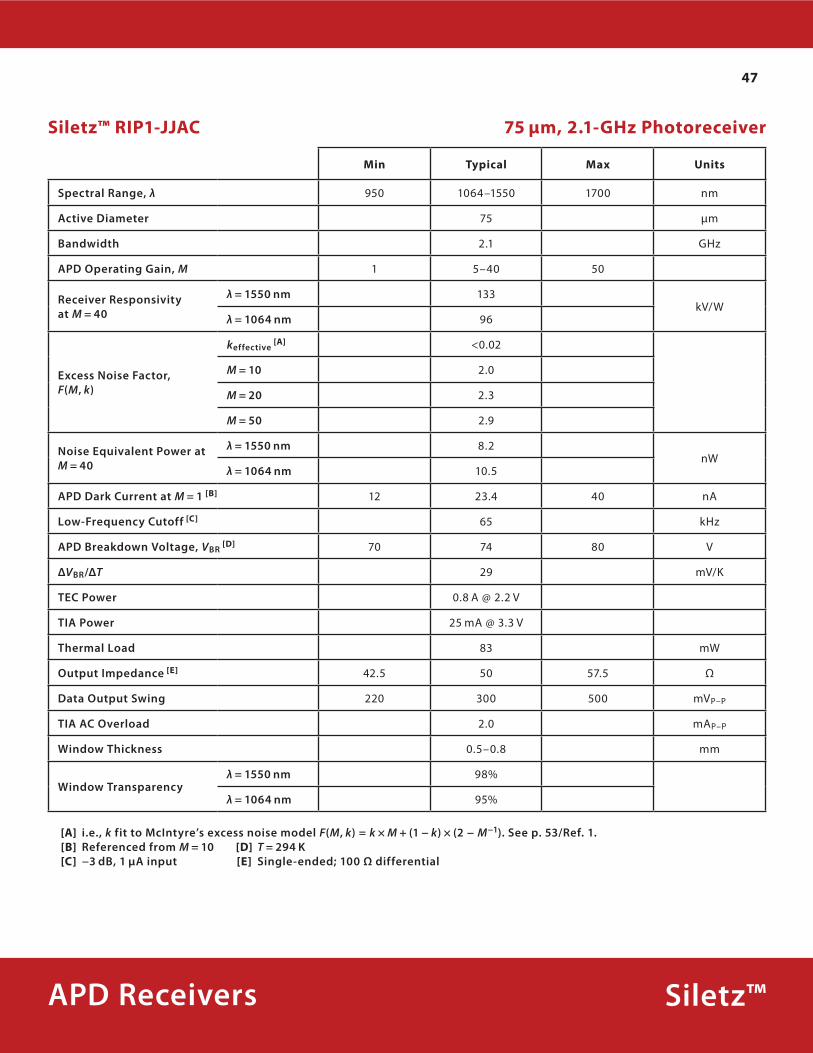
Siletz™ RIP1-JJAC 75 µm, 2.1-GHz Photoreceiver
48
Siletz™APD Receivers
2.488 Gb/s
622 Mb/s
156 Mb/s
2.125 Gb/s
Bit Rate
–50 –45 –40 –35
10–1
10–2
10–3
10–4
10–5
10–6
10–7
10–8
10–9
10–10
10–11
10–12
Bit
Err
or R
ate
Optical Power [dBm]
Siletz™ RIP1-JJAC
Siletz™ RIP1-JJQC
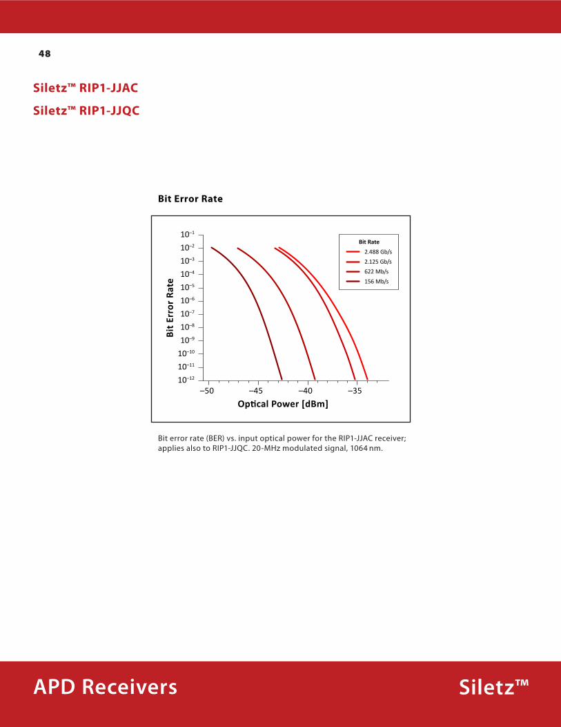
Bit Error Rate
Bit error rate (BER) vs. input optical power for the RIP1-JJAC receiver; applies also to RIP1-JJQC. 20-MHz modulated signal, 1064 nm.
49
Siletz™APD Receivers
Min Typical Max Units
Spectral Range, λ 950 1064–1550 1700 nm
Active DiameterActual 75
µmEffective 300
Bandwidth 1.5 GHz
APD Operating Gain, M 1 5–40 50
Receiver Responsivity at M = 40
λ = 1550 nm 311kV/W
λ = 1064 nm 225
Excess Noise Factor, F(M, k)
keffective [A] <0.02
M = 10 2.0
M = 20 2.3
M = 50 2.9
Noise Equivalent Power at M = 30
λ = 1550 nm 11.0nW
λ = 1064 nm 14.1
Noise Equivalent Power at M = 40
λ = 1550 nm 12.5nW
λ = 1064 nm 15.8
APD Dark Current at M = 1 [B] 12 23.4 40 nA
Low-Frequency Cutoff [C] 30 kHz
APD Breakdown Voltage, VBR [D] 70 74 80 V
ΔVBR/ΔT 29 mV/K
TIA Power 20 mA @ 3.3 V 24 mA @ 4.5 V
Thermal Load 66 108 mW
Output Impedance [E] 50 Ω
Data Output Swing 140 270 mVP–P
TIA AC Overload [F] 8 mAP–P
Lens Transparencyλ = 1550 nm 98%
λ = 1064 nm 95%
[A] i e , k fit to McIntyre’s excess noise model F(M, k) = k × M + (1 − k) × (2 − M−1) See p 53/Ref 1 [B] Referenced from M = 10 [E] Single-ended; 100 Ω differential [C] −3 dB, 1 µA input [F] At RTIA input [D] T = 294 K
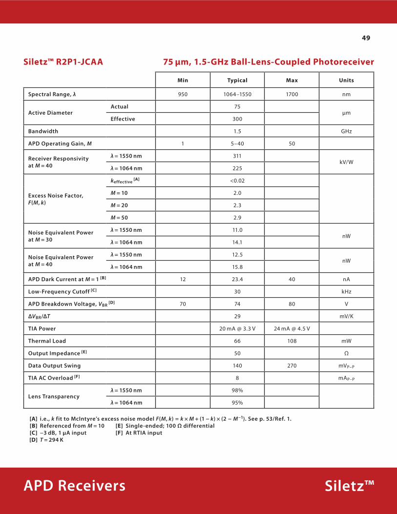
Siletz™ R2P1-JCAA 75 µm, 1.5-GHz Ball-Lens-Coupled Photoreceiver
50
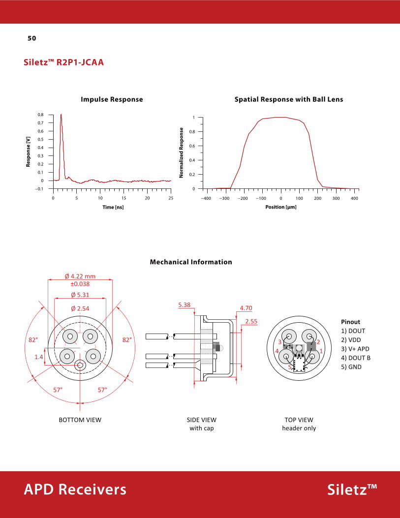
Siletz™APD Receivers
Siletz™ R2P1-JCAA
Mechanical Information
Impulse Response Spatial Response with Ball Lens
Pinout1) DOUT2) VDD3) V+ APD4) DOUT B5) GND
111
Ø 5.31
1.4
Ø 4.22 mm±0.038
5
123
4
57°57°
82° 82°
Ø 2.54
2.55
4.705.38
BOTTOM VIEW SIDE VIEWwith cap
TOP VIEWheader only
0 5 10 15 20 25
0.8
0.7
0.6
0.5
0.4
0.3
0.2
0.1
0
−0.1
Time [ns]
Resp
onse
[V]
−400 −300 −200 −100 0 100 200 300 400
1
0.8
0.6
0.4
0.2
0
Position [µm]
Nor
mal
ized
Res
pons
e
51
Siletz™APD Receivers
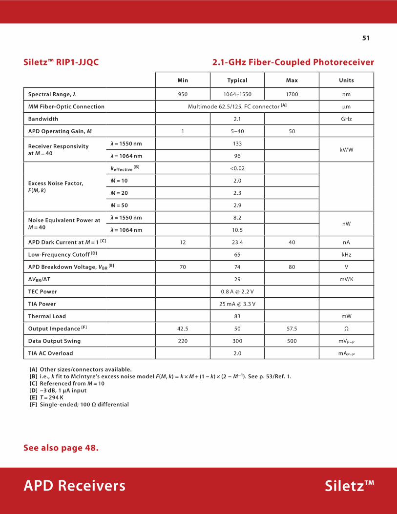
Siletz™ RIP1-JJQC 2.1-GHz Fiber-Coupled Photoreceiver
Min Typical Max Units
Spectral Range, λ 950 1064–1550 1700 nm
MM Fiber-Optic Connection Multimode 62.5/125, FC connector [A] µm
Bandwidth 2.1 GHz
APD Operating Gain, M 1 5–40 50
Receiver Responsivity at M = 40
λ = 1550 nm 133kV/W
λ = 1064 nm 96
Excess Noise Factor, F(M, k)
keffective [B] <0.02
M = 10 2.0
M = 20 2.3
M = 50 2.9
Noise Equivalent Power at M = 40
λ = 1550 nm 8.2nW
λ = 1064 nm 10.5
APD Dark Current at M = 1 [C] 12 23.4 40 nA
Low-Frequency Cutoff [D] 65 kHz
APD Breakdown Voltage, VBR [E] 70 74 80 V
ΔVBR/ΔT 29 mV/K
TEC Power 0.8 A @ 2.2 V
TIA Power 25 mA @ 3.3 V
Thermal Load 83 mW
Output Impedance [F] 42.5 50 57.5 Ω
Data Output Swing 220 300 500 mVP–P
TIA AC Overload 2.0 mAP–P
[A] Other sizes/connectors available [B] i e , k fit to McIntyre’s excess noise model F(M, k) = k × M + (1 − k) × (2 − M−1) See p 53/Ref 1 [C] Referenced from M = 10 [D] −3 dB, 1 µA input [E] T = 294 K [F] Single-ended; 100 Ω differential
See also page 48.
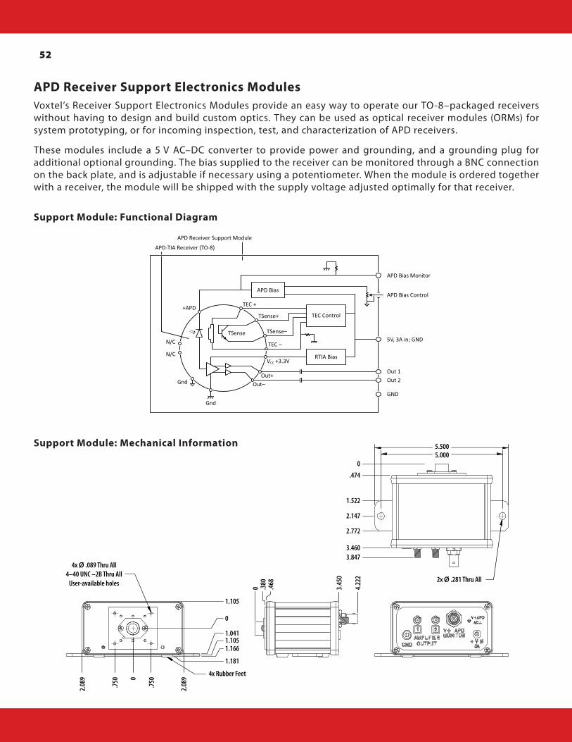
52
APD Receiver Support Electronics ModulesVoxtel’s Receiver Support Electronics Modules provide an easy way to operate our TO-8–packaged receivers without having to design and build custom optics. They can be used as optical receiver modules (ORMs) for system prototyping, or for incoming inspection, test, and characterization of APD receivers.
These modules include a 5 V AC–DC converter to provide power and grounding, and a grounding plug for additional optional grounding. The bias supplied to the receiver can be monitored through a BNC connection on the back plate, and is adjustable if necessary using a potentiometer. When the module is ordered together with a receiver, the module will be shipped with the supply voltage adjusted optimally for that receiver.
VCC +3.3V
TEC –
TEC +
APD-TIA Receiver (TO-8)
APD Receiver Support Module
RTIA Bias
APD Bias
APD Bias Monitor
APD Bias Control
5V, 3A in; GND
Out 1
GND
Out 2
TEC ControlTSense+
TSense–
+APD
Gnd
Gnd
N/C
Out+
Out–
N/C
TSense
4x Ø .089 Thru All4–40 UNC –2B Thru All
User-available holes 2x Ø .281 Thru All
2.08
9
.750 0
.750
2.08
9
1.166
1.181
4x Rubber Feet
1.1051.041
0
1.105
0 .380
.468
3.45
0
4.22
2
5.0005.500
0
.474
1.522
2.147
2.772
3.4603.847
Support Module: Functional Diagram
Support Module: Mechanical Information
53
[1] R. J. McIntyre, “Multiplication Noise in Uniform Avalanche Diodes,” IEEE Transactions on Electron Devices 13(1), 164–168 (1966).
[A] G. M. Williams, “GHz-Rate Single-Photon-Sensitive Linear-Mode APD Receivers,” Proceedings of SPIE 7222, 72221L (2009).
[B] G. M. Williams, M. A. Compton, and A. S. Huntington, “High-Speed Photon Counting with Linear-Mode APD Receivers,” Proceedings of SPIE 7320, 732012 (2009).
References
Single-Photon Counting: Voxtel Publications

[A] R. J. McIntyre, “A New Look at Impact Ionization — Part I: A Theory of Gain, Noise, Breakdown Probability, and Frequency Response,” IEEE Transactions on Electron Devices 46(8), 1623–1631 (1999).
[B] P. Yuan, K. A. Anselm, C. Hu, H. Nie, C. Lenox, A. L. Holmes, B. G. Streetman, J. C. Campbell, and R. J. McIntyre, “A New Look at Impact Ionization — Part II: Gain and Noise in Short Avalance Photodiodes,” IEEE Transactions on Electron Devices 46(8), 1632–1639 (1999).
[C] M. A. Saleh, M. M. Hayat, B. E. A. Saleh, and M. C. Teich, “Dead-Space-Based Theory Correctly Predicts Excess Noise Factor for Thin GaAs and AlGaAs Avalanche Photodiodes,” IEEE Transactions on Electron Devices 47(3), 625–6333 (2000).
[a] G. M. Williams, “GHz-Rate Single-Photon-Sensitive Linear-Mode APD Receivers,” Proceedings of SPIE 7222, 72221L (2009).
[b] G. M. Williams, M. A. Compton, and A. S. Huntington, “High-Speed Photon Counting with Linear-Mode APD Receivers,” Proceedings of SPIE 7320, 732012 (2009).
©Voxtel, Inc 2011