volume 29 number 3 bulletin is it demon who elevates the
TRANSCRIPT

ASSOCIATION OF ASIA PACIFIC PHYSICAL SOCIETIES
V o l u m e 2 9 | N u m b e r 3 | J U N E 2 0 1 9 Bulletin
Is it Demon who Elevates the Electron?
APCTP Section● Magnetization Plateaus in a
Geometrically Frustrated Anisotropic Four-Leg Nanotube
● Rede� ning SI Base Units with Fundamental Constants
Feature Articles● Sensing Molecules and Electrons Using Nanostructured
Materials and Devices ● Single-Electron-Resolution Noise Analysis and
Application Using High-Sensitivity Charge Sensor● Application of a Plasmonic Chip for Sensitive Biodetection● Nanoscale, Low-energy Molecular Sensors for Health Care
and Environmental Monitoring● New Research Project with Muon Beams for Neutrino
Nuclear Responses and Nuclear Isotopes Production
Society News● The Physical Society of Japan
Announces the Recipients of the 24th Outstanding Paper Award
● Recent Activities of the Division of Astrophysics Cosmology and Gravitation (DACG)
ISSN: 0218-2203

Supported by:
BORNEO CONVENTION CENTREKuching - Sarawak, Malaysia
17 - 22 November 2019
PHYSICS CONFERENCE(APPC14)
14 th ASIA - PACIFIC
PHYSICS CONFERENCE(APPC14)
14 th ASIA - PACIFIC
(Malaysian Institute of Physics)
Sarawak,Land of the Hornbills,
warmly welcomes you!
Sarawak,Land of the Hornbills,
warmly welcomes you!
website : http://appc2019.ifm.org.my/email : [email protected]
Kuching (means ’cat’).The capital city, nestled on thebanks of Sarawak River, offers
modern and rustic charms.

Association of Asia Pacific Physical Societies
Editorial Board MEMBErs
Past Editors-in-ChiEf shoji nagamiya / 2014. 01 - 2017. 06 RIKEN, 2-1 Hirosawa, Wako, Saitama 351-0198, JapanE-mail: [email protected]
Won namkung /2011. 01 - 2014. 06POSTECH, 77 Cheongam-Ro, Nam-gu Pohang 790-784, KoreaE-mail: [email protected]
W-Y. Pauchy hwangNational Taiwan University, Taipei 106E-mail: [email protected]
s. C. limFaculty of Engineering Multimedia University Cuberjaya, Selangor, MalaysiaE-mail: [email protected]
Editorial staff
seunglae Cho (aPCtP)Email: [email protected]
Eunjeong lee (aPCtP)Email: [email protected]
susan song-one KangPrincipal Language and Technical Editor
Gui-lu long (Beijing) / PresidentTsinghua University, Haidian District, Beijing 100084E-mail: [email protected]
fu-Jen Kao (taipei) / Vice President National Yang-Ming University, No.155, Sec.2, Linong Street, Taipei, 112 E-mail: [email protected] Jun'ichi Yokoyama (Japan) / secretary RESCEU, The University of Tokyo, Hongo Bunkyo-ku, Tokyo 113-0033, JapanE-mail: [email protected]
hyoungJoon Choi (Korea) / treasurerYonsei University, 50 Yonsei-ro, Seodaemun-gu, Seoul, KoreaE-mail: [email protected]
seunghwan Kim (Korea) / special advisorPOSTECH, 77Cheongam-Ro Nam-gu, Pohang, Gyeongbuk, 37673, KoreaE-mail: [email protected]
Cathy foley (australia) CSIRO, Bradfield Road West Lindfield NSW 2070, AustraliaE-mail: [email protected]
Kuijuan Jin (Beijing) Institute of Physics, Chinese Academy of Sciences P.O. Box 603, Beijing 100190E-mail: [email protected]
Xing Zhu (Beijing) Peking University, No. 5 Yiheyuan Road, Haidian District, Beijing, 100871E-mail: [email protected]
CoUnCil MEMBErs (2017-2019)
ruiqin Zhang (hong Kong)Department of Physics and Materials ScienceCity University of Hong Kong G6702, 6/F, Academic 1, Tat Chee Avenue, Kowloon, Hong Kong SARE-mail: [email protected]
hatsumi Mori (Japan) ISSP, The University of Tokyo, Hongo Bunkyo-ku, Tokyo 113-0033, JapanE-mail: [email protected]
Masaaki tanaka (Japan) Spintronics Center, The University of Tokyo, Hongo Bunkyo-ku, Tokyo 113-0033, JapanE-mail: [email protected] sang Pyo Kim (Korea) Kunsan National University, 558 Daehak-ro, Kunsan 573-701, KoreaE-mail: [email protected]
Kurunathan ratnavelu (Malaysia)Department of Physics, University of Malaya, 50603 Kuala Lumpur, Malaysia E-mail: [email protected]
rajdeep singh rawat (singapore)National Institute of Education, Singapore (NIE), 1 Nanyang Walk, Singapore 637616E-mail: [email protected]
Minn-tsong lin (taipei)National Taiwan University 10617, TaipeiE-mail: [email protected] nguyen Quang liem (Vietnam) Vietnam Academy of Science and Technology 18 Hoang Quoc Viet Rd. Hanoi, VietnamE-mail: [email protected]
tohru Motobayashi (Editor-in-Chief) / 2017.01-2020.06RIKEN Nishina Center for Accelerator-Based Science2-1, Hirosawa, Wako, Saitama 351-0198, JapanEmail: [email protected]
akira Yamada (deputy Editor-in-Chief) / 2017.01-2020.06Tokyo Institute of Technology, 2-12-1 Ookayama, Meguro-ku, Tokyo, 152-8550, JapanEmail: [email protected]
Qing Wang / 2017.01-2020.06Tsinghua University, Haidian District Beijing 100084E-mail: [email protected]
Brian James / 2017.01-2020.06Sydney University, New South Wales 2006 AustraliaE-mail: [email protected]
leong Chuan Kwek / 2017.01-2020.06Center for Quantum TechnologiesNational University of Singapore, Block S153 Science Drive 2, 117543, SingaporeE-mail: [email protected]
shozo suto / 2017.01-2020.06Graduate School of Science, Tohoku University6-3, Aramaki Aza-Aoba, Aoba-ku, Sendai 980-8578, JapanEmail: [email protected]
Jeong-hyeon song / 2017.01-2020.06School of Physics, Konkuk University120 Neungdong-ro, Gwangjin-gu, Seoul, KoreaEmail: [email protected]
Chong-sun Chu / 2017.01-2020.06National Center for Theoretical Sciences101, Section 2 Kuang Fu Road, Hsinchu, 300Email: [email protected]
Jan-e alam / 2017. 10-2020.09Variable Energy Cyclotron Centre, 1/AF Bidhannagar, Kolkata - 700 064, INDIAEmail: [email protected]
Kaoru Minoshima / 2019.04-2020.03The University of Electro-Communications (UEC)1-5-1 Chofugaoka, Chofu, Tokyo 182-8585 JAPANEmail: [email protected]

16
35
41
48
46
ContEntsJune 2019 Vol. 29 No. 3
3
4
10
16
21
27
29
35
41
43
46
48
56
61
fEatUrE artiClEs [Guest editor: Yutaka Majima]
Sensing Molecules and Electrons Using Nanostructured Materials and Devices | Yutaka Majima
Single-Electron-Resolution Noise Analysis and Application Using High-Sensitivity Charge Sensor |Katsuhiko Nishiguchi, Kensaku Chida, Akira Fujiwara
Application of a Plasmonic Chip for Sensitive Biodetection |Keiko Tawa
Nanoscale, Low-energy Molecular Sensors for Health Care and Environmental Monitoring |Ken Uchida, Takahisa Tanaka
New Research Project with Muon Beams for Neutrino Nuclear Responses and Nuclear Isotopes Production |Izyan Hazwani Hashim, Hiro Ejiri
aCtiVitiEs and rEsEarCh nEWsFASER: CERN Approves New Experiment to Look for Long-lived, Exotic Particles |By Cristina Agrigoroae [Reproduced from the e-EPS]
institUtEs in asia PaCifiCAdvanced Science Research Center Japan Atomic Energy Agency | Makoto Oka, Hiroyuki Koura
The Institute for Solid State Physics at The University of Tokyo |Hatsumi Mori
PhYsiCs foCUsHelical Ordering of Spin Trimers Found in a Distorted Kagome Lattice | Takeshi Matsumura
soCiEtY nEWsThe Physical Society of Japan Announces the Recipients of the 24th Outstanding Paper Award |
Recent Activities of the Division of Astrophysics Cosmology and Gravitation (DACG) |Misao Sasaki
aPCtP sECtionMagnetization Plateaus in a Geometrically Frustrated Anisotropic Four-Leg Nanotube |Rouhollah Jafari, Saeed Mahdavifar, and Alireza Akbari
Redefi ning SI Base Units with Fundamental Constants |Ho-Seong Lee
CalEndar of EVEnts

3
JUNE 2019 VOL. 29 NO. 3 fEatUrE artiClEs
The sensitivities to detect molecules and electrons are enhanced by introductions of nanostruc-tured materials. The three feature articles of this issue present and review research regarding this enhancement through multimolecular gas sensors, cell imaging, and single-electron motion sen-sors based on functionalized graphene, a periodic structure, and an ultra-narrow channel, respec-tively.
Prof. Uchida describes two types of molecular sensors based on Pd-functionalized suspended graphene and Pt nanosheets, respectively. Owing to its suspended structure, the temperature of graphene can change and be controlled very quickly, simply by changing the bias voltage, which results in the detection of H2O and H2 in the air. Prof. Tawa shows clear fluorescence images of neuronal cells enhanced by surface plasmon resonance. Various plasmon chips based on periodic metallic patterns with a wavelength-scale have been prepared and improved. The mechanism of the enhanced fluorescence by surface plasmons on plasmon chips is discussed. Dr. Nishiguchi demonstrates single-electron-resolution noise analysis by using a 10 nm-sized Si wire field-effect transistor at room temperature. They report a suppression of shot noise in a small capacitor under non-equilibrium conditions. The paradox of Maxwell’s demon, which is an imaginary entity re-ducing the entropy of a system and generating free energy in the system, is also demonstrated by real-time monitoring of single-electron motion.
The following three feature articles focus on research that has contributed to the enhancement of the sensitivity of sensors by the introduction of nanostructures. We are pleased to introduce to the readers of the AAPPS Bulletin these interdisciplinary areas of research.
Sensing Molecules and Electrons Using Nanostructured Materials and Devices
YUTAKA MAJIMA LAborATorY for MATerIALS And STrUcTUreS, ToKYo InSTITUTe of TechnoLogY
Yutaka Majima is a professor at the Laboratory for Materials and Structures, Tokyo Institute of Technology (Tokyo Tech). He received his PhD in engineering from Tokyo Tech. He was the chief executive editor of Applied Physics Express (APEX) and the Japanese Journal of Applied Physics (JJAP) in 2017. His professional interests are in nanoscale science and devices.

4
BULLETINfEatUrE artiClEs
ABSTRACT
We introduce an analysis of thermal noise using a high-sensitivity charge sensor. Since the sensor is based on a Si field-effect transistor whose channel size is approximately 10 nm, the sensor exhibits sufficiently high sensitivity to detect single-electron motion even at room temperature. By connecting this sensor to a small capacitor comprising dynamic random access memory, thermal noise in the capacitor can be monitored in real time with single-elec-tron resolution. Such real-time monitoring reveals that when the capacitor is sufficiently small that the charging energy for storing one electron in the capacitor is greater than the thermal energy, the thermal noise is suppressed and enhanced. This represents a deviation from the law of energy equipartition. In addition to this noise analysis, we present a successful demonstration of power genera-tion using an analogy of Maxwell’s demon that detects and manipulates single-electron motion, which should accelerate research in the field of thermodynamics. These experimental results show that the high-sensitivity charge sensor can function as a superior platform for mi-croscopic analysis of noise, small electronic devices, and thermodynamics as well as a demonstration of theoreti-cal expectation in basic research.
INTRODUCTION
Data processing circuits comprise a huge number of Si field-effect transistors (FETs) and their miniaturization has increased circuit performance. FETs have also been used as a signal amplifier or sensor for various kinds of applications such as memory circuits, image sensors, and chemical sensors. Si-FET sensors are advantageous
due to their superior integration and miniaturization capabilities. In particular, the currently employed min-iaturization technique established for data processing circuits achieves a nanometer-scale structure enabling a sufficiently high level of sensor sensitivity [1, 2] to detect an extremely small number of objects including proteins [3, 4], DNA [5], and ultimately a single charge [6]. Such improvement in the sensor sensitivity provides various merits to not only practical applications but also basic research. Some such merits for practical applications are high-resolution signal detection, fast sensing, and highly dense integration. Up-coming applications such as the quantum computers and quantum key distributions have also relied on highly sensitive sensors with single-elec-tron and single-photon resolution. In the fields of basic research, high-sensitivity sensors have played important roles in revealing new phenomena and physics, and are vital to academics and applications in the future.
In this paper, we introduce analysis on electric noise us-ing a Si-FET-based sensor. Since the sensor is sufficiently small to detect single electrons, noise analysis can be car-ried out with single-electron. Although single-electron detection reported elsewhere have been carried out at low temperature, miniaturization of the Si-FET-based sensor allows room-temperature operation. Additionally, a unique application taking advantage of single-electron detection, i.e., Maxwell’s demon, is also shown.
Single-Electron-Resolution Noise Analysis and Application Using High-Sensitivity Charge Sensor
KATSUhIKo nIShIgUchI,* KenSAKU chIdA, And AKIrA fUJIwArA nTT bASIc reSeArch LAborATorIeS, nTT corPorATIon, 3-1 MorInoSATo wAKAMIYA,
ATSUgI, KAnAgAwA 243-0198 JAPAn
doI: 10.22661/AAPPSbL.2019.29.3.04
*E-mail address: [email protected]

5
JUNE 2019 VOL. 29 NO. 3 fEatUrE artiClEs
FET-BASED SENSOR WITH SINGLE-ELECTRON RESOLUTION
Single-electron-resolution electric-noise analysis is car-ried out using a Si-FET-based sensor integrated with dy-namic random access memory (DRAM) comprising one FET and one storage capacitor (SC) as shown in Fig. 1 [6]. By controlling the FET with word and bit lines, elec-trons are stored in or released from the SC and absence/existence of electrons in the SC is usually represented as one bit of information. Since the resistance of the FET is not infinite even in its off state, electrons are randomly shuttled between the SC and bit line due to thermal en-ergy, which causes the thermal noise in the SC. In our analysis, this electron shuttling, i.e., thermal noise, is monitored with single-electron resolution using the sen-sor. Electrons in the SC modulate the current flowing through the sensor due to repulsive force between the electrons in the SC and those in the sensor channel. A key point for single-electron monitoring is the degree of current modulation, dImodulation. Following conventional noise analysis, we consider voltage noise Vnoise instead of electron shuttling. In the most likely case that Vnoise is suf-ficiently low to modulate the current flowing through the sensor linearly, dImodulation can be given by
dImodulation = gm (CSC-channel/Cgate)dVnoise, (1)
where gm is the sensor transconductance defined as a gra-dient of current characteristics as a function of the gate voltage of the sensor, and CSC-channel and Cgate are the ca-pacitance between the SC and a tiny channel of the FET-based sensor and that between the gate and tiny channel, respectively, as shown in Fig. 1(c). To increase dImodulation, we must consider the following points. Transconductance
gm increases with the voltage between the source and drain electrodes of the sensor. Capacitances CSC-channel and CSC-channel/Cgate are increased by locating the tiny channel very close to the SC and by reducing the size of the tiny channel, respectively. In our experience, the typical size of the tiny channel of the sensor is approxi-mately 10 nm so that it can detect a single electron. Such a small size allows the sensor to behave as a single-electron transistor [7] at low temperature. Some reports show that single-electron transistors have good sensitiv-ity characteristics due to their low background noise [2]. However, since single-electron transistors can operate at low voltages between the source and drain electrodes, gm is low. Room-temperature operation is also extremely dif-ficult. Therefore, we use the sensor based not on a single-electron transistor but on a conventional FET.
On the other hand, since Vnoise is caused by fluctuation dQ of the charge in the capacitor, dVnoise can be given by
dVnoise = dQ /CSC, (2)
where CSC is the total capacitance of the SC. When the sensor detects a single electron, dQ is e, where e is the el-ementary charge of 1.6 × 10⁻¹⁹ C. From the viewpoint of experiments at room temperature, typical CSC and Vnoise values are 10 aF and 16 mV, respectively, which means that the SC size must be approximately 10 nm.
As mentioned above, the success of single-electron-resolution noise analysis is entirely dependent on how the small structure of approximately 10 nm is achieved. While various kinds of essentially small materials such as carbon nanotubes, graphene, and two-dimensional tran-sition metal dichalcogenides have been studied, we take
fig. 1: Si-FET-based sensor integrated with DRAM. (a) SEM image. Entire area is covered with a gate electrode as shown in (b). (b) Birds-eye view. (c) Equivalent circuit.

6
BULLETINfEatUrE artiClEs
advantage of well-established Si-transistor fabrication processes guaranteeing high reproducibility, further min-iaturization, and high integrability. In order to achieve a small structure of approximately 10 nm, we used silicon-on-insulator wafers and shrank the electron-beam-pat-terned fine structure using an oxidation process [6].
SINGLE-ELECTRON-RESOLUTION ANALYSIS OF THERMAL NOISE
Figure 2 shows the change in the current flowing through an FET-based sensor when constant voltage is applied to all electrodes, which means that the DRAM is under an equilibrium condition. A change in the current shows a step-like pattern in which the step height is almost con-stant. This represents the situation when a single electron enters and leaves the SC. The current respectively de-
creases and increases by a constant quantity, which means that the sensor monitors electron shuttling between the SC and bit line in real time, and more importantly, at room temperature.
By using the change in current to represent electron shuttling as shown in Fig. 2, we can discuss the electron shuttling, i.e., thermal noise, statistically. As shown in Fig. 3(a), a histogram of deviation Nelectron from the average of the number of electrons in the SC exhibits a Gaussian function. Since e/CSC multiplied by Nelectron corresponds to the voltage noise in the capacitor, the histogram also represents a distribution of voltage-noise amplitude. Additionally, Fig. 3(b) shows that a variance in the distri-bution of the voltage-noise amplitude, or mean-square voltage noise, follows the temperature dependence given by kBT /CSC, where kB is Boltzmann’s constant and T is temperature. This dependence is one of the well-known features of thermal noise. Another important signature of thermal noise is that interval dt of the current pla-teaus, in which electrons remain in the capacitor, are always random as shown in Fig. 2. Indeed, the frequency spectrum density of the voltage noise evaluated from temporal change in Nelectron multiplied by e/CSC exhibits flat characteristics up to the cut-off frequency as shown in Fig. 3(c). These features mean that single-electron mo-tion follows the well-known thermal noise model.
When CSC is so low that charging energy e2/2CSC for a single electron to be stored in the capacitor is greater than thermal energy kBT /2, noise originating from the electron shuttling does not exhibit the well-known fea-tures of thermal noise [9]. As mentioned above, since
fig. 2: Current flowing through FET-based sensor. Voltages applied to all electrodes are constant. The details are given in [8]. Nelectron is a deviation from the average of the number of electrons in the SC and dt is the interval during which electrons stay at the SC without electron injection/ejection.
fig. 3: (a) Histogram of deviation Nelectron from the average of the number of electrons in the SC. The solid line is the Gaussian function theoretically expected from thermal-noise model. (b) Dependence of Mean-square noise voltage in the SC, evaluated from a variance of the distribution of voltage-noise amplitude given by Nelectron e /C SC, on temperature. The solid line is given by kBT /C SC. (c) Power spectrum density of voltage noise evaluated from temporal change in Nelectron multiplied by e /C SC. In order to channel resistance of FET, voltage applied to the bit line is changed. The solid line represents theoretical values. Details are given in [9].

7
JUNE 2019 VOL. 29 NO. 3 fEatUrE artiClEs
thermal noise follows kBT /CSC, which is the so-called kT/C noise, reduction in CSC increases the noise and thus dis-turbs the degree of device shrinkage especially in analog circuits. However, when CSC becomes lower than e2/kBT, noise deviates from values given by kBT /CSC as shown in Fig. 4. The reason for this deviation is the Coulomb blockade [7], in which high charging energy in the ca-pacitor suppresses unintentional electron shuttling driv-en by thermal energy. The degree of deviation depends on the difference between the electro-chemical potential of the capacitor and the Fermi energy of the bit line of the DRAM. In other words, while electron motion driven by thermal energy follows the law of energy equiparti-tion at e2/2CSC < kBT /2, an extremely small capacitor at e2/2CSC < kBT /2 gives arise to a deviation from the law of energy equipartition. It should be noted that since this unique insight of thermal noise appears when the capaci-tance (or material dimension) reaches aF (or 10 nm) or less, any small material including carbon nanotubes, gra-phene, and molecules, also face the same phenomenon, i.e., deviation from the law of energy equipartition.
MAXWELL’S DEMON UTILIZING SINGLE-ELECTRON MOTION
Single-electron-resolution noise analysis highlights new insight into noise. On the other hand, real-time monitor-ing of single-electron motion allows us to demonstrate Maxwell’s demon, which is an imaginary entity reducing the entropy of a system and generating free energy in the
system. One famous example is the separation of hotter and colder gas particles in a box. The demon can iden-tify randomly moving gas particles, their temperatures, and open/close a gate in the box to separate the hotter and colder particles, which creates a temperature differ-ence and thus generates energy. This paradox, in which the second law of thermodynamics seems to be violated, had been clarified by the context of information thermo-dynamics [10].
The point of operation driven by Maxwell’s demon is to identify the individual gas particles. In the same analogy, when gas particles are replaced with electrons by using a single-electron-resolution sensor, electric energy would be generated. For this operation, the sensor integrated with FETs functioning as a gate separating electrons was fabricated as shown in Fig. 5 [11]. The sensor monitors the number of electrons in the box between two FETs. When the left FET opens and an electron enters the box due to thermal energy, the left FET is closed and thus the electron is stored in the box. Then, when the right FET opens and an electron leaves the box, the right FET is closed. Consequently, electrons can flow from the left side to the right side although no energy is applied to the electron, i.e., current generation by Maxwell’s de-mon. Even when the potential of the right side is higher than that of the left side, electrons can climb the poten-tial because of thermal energy and thus gain energy. Re-peating this operation generates electric power.
fig. 4: C SC dependence on voltage noise in the SC. Closed squares and open circles are experimental values and those given by kBT /C SC. The solid lines and shaded area represent expected voltage noise considering the charging energy and thermal energy. Details are given in [9].

8
BULLETINfEatUrE artiClEs
Experimental demonstration of Maxwell’s demon had been very difficult because of the extreme difficulty in identifying a single particle such as gas particles and elec-trons whose motion is driven by thermal energy. How-ever, recently, single-electron transistors that can detect and manipulate single electrons have provided success-ful demonstration of Maxwell’s demon utilizing single electrons [12]. The FET-based sensor described herein that detects single-electron motion has also succeeded in demonstrating this but, more importantly, at room tem-perature. Therefore, we believe that study on information thermodynamics would be accelerated by ultra-high sen-sitivity sensors and provide a hint toward achieving ultra-low-power consumption electric devices because informa-tion thermodynamics relates to the Landauer limit, which
relates to the power consumption limit of digital circuits.
CONCLUSION
Thermal noise was analyzed with single-electron resolu-tion. Thanks to its statistical analysis, we have observed unique features in which thermal noise in a small capaci-tor is suppressed and enhanced. This thermal noise orig-inates from random electron motion under an equilibri-um condition. In addition to thermal noise, suppression of shot noise under non-equilibrium conditions has also been reported [13]. Therefore, we believe that analysis of electron transport with single-electron resolution would highlight new insights in future electric devices of small dimensions.
fig. 5: (a) Schematics of a demonstration of Maxwell’s demon. Maxwell’s demon can monitor single-electron motion and open/close two gates according to electron’s position. (b) Fabricated devices and (c) its schematics. Two transistors function as gates. (d) Change in current generated by Maxwell’s demon when potential height of the right side to which electrons go is changed (see 5(a)). The solid and dotted lines represent simulated values.

9
JUNE 2019 VOL. 29 NO. 3 fEatUrE artiClEs
akira fujiwara is a senior distinguished scientist and a senior manager of Physical Science Laboratory at NTT Basic Research Laboratories. He received his Ph.D. degree in applied physics from The University of Tokyo in 1994. He is currently working on silicon nanodevices for ultimate electronics. He is a member of the Japan Society of Applied Physics and an IEEE fellow.
Kensaku Chida is a research scientist at NTT Basic Research Laboratories, Nippon Telegraph and Telephone Corporation, Kanagawa, Japan. He received his Ph.D. in chemistry from Kyoto University in 2013. He is interested in stochastic thermodynamics of single-electrons in nanometer-scale devices.
Katsuhiko nishiguchi is a distinguished scientist at NTT Basic Research Laboratories, Nippon Telegraph and Telephone Corporation, Kanagawa, Japan. he received his Ph.D. in electrical engineering from Tokyo Institute of Technology, Japan in 2002. He is experimental researcher of applied physics for semiconductor devices.
Additionally, we demonstrated Maxwell’s demon by tak-ing advantage of the sensor feature of detecting single-electron motion as well as FET manipulation of it. Since the sensor operates even at room temperature, it can be used as a platform for studying fields such as informa-tion thermodynamics and electronics. Using such single-electron detection and manipulation, electric circuits using single electrons has also been achieved [14-20]. Therefore, Si FETs miniaturized by their ever-advancing fabrication techniques promise to open new fields of ba-sic research and applications.
References
[1] M. J. Madou and r. cubicciotti: Proc. Ieee 91 (2003) 830.[2] M. h. devoret and r. J. Schoelkopf: nature 406 (2000) 1039.[3] Y. chui, Q. wei, h. park, and c. M. Lieber: Science 293 (2001) 1289.[4] e. Stern, J. f. Klemic, d. A. routenberg, P. n. wyrembak, d. b. Turner-evans, A.
d. hamilton, d. A. LaVan, T. M. fahmy, and M. A. reed: nature 445 (2007) 519.
[5] J. hahm and c. M. Lieber: nano Lett. 4 (2004) 51.
[6] K. nishiguchi, c. Koechlin, Y. ono, A. fujiwara, h. Inokawa, and h. Yamaguchi: Jpn. J. Appl. Phys. 47 (2008) 8305.
[7] K. K. Likharev: IbM J. res. dev. 32 (1988) 144. [8] K. nishiguchi, Y. ono, and A. fujiwara: nanotechnology 25 (2004) 275201.[9] P. A. carles, K. nishiguchi, and A. fujiwara: Jpn. J. Appl. Phys. 54 (2015)
06fg03.[10] T. Sagawa and M. Ueda: Phys. rev. Lett. 102 (2009) 250602.[11] K. chida, S. desai, K. nishiguchi, and A. fujiwara: nat. commun. 8 (2017)
15310.[12] J. Koski, V. Maisi, T. Sagawa, and J. Pekola: Phys. rev. Lett. 113 (2014)
030601.[13] K. nishiguchi, Y. ono, and A. fujiwara: Appl. Phys. Lett. 98 (2011) 193502.[14] K. nishiguchi, Y. ono, A. fujiwara, h. Yamaguchi, h. Inokawa, and Y.
Takahashi: Appl. Phys. Lett. 90 (2007) 223108.[15] K. nishiguchi, h. Inokawa, Y. ono, A. fujiwara, and Y. Takahashi: Appl. Phys.
Lett. 85 (2004) 1277.[16] K. nishiguchi, A. fujiwara, Y. ono, h. Inokawa, and Y. Takahashi: Appl. Phys.
Lett. 88 (2006) 183101.[17] K. nishiguchi, A. fujiwara, Y. ono, h. Inokawa, and Y. Takahashi: Appl. Phys.
Lett. 90 (2007) 223108.[18] K. nishiguchi, Y. ono, A. fujiwara, h. Inokawa, and Y. Takahashi: Appl. Phys.
Lett. 92 (2008) 062105.[19] K. nishiguchi and A. fujiwara: nanotechnology 20 (2009) 175201. [20] K. nishiguchi and A. fujiwara: Jpn. J. Appl. Phys. 50 (2011) 06gf04.

10
BULLETINfEatUrE artiClEs
ABSTRACT
Enhanced fluorescence is a powerful tool for the sensi-tive detection of analytes. A plasmonic chip is a substrate covered with a thin metal film and has a surface includ-ing a periodic pattern with a wavelength-scale pitch. It can make the fluorescence from a fluorescent molecule attached to a plasmonic chip enhance by 100 times and the enhanced fluorescence is based on the excita-tion of the grating-coupled surface plasmon resonance (GC-SPR) field. In this work, the structure of a plasmonic chip, the mechanism of fluorescence enhancement, and the application of a plasmonic chip to sensitive immu-nosensor and cell imaging will be introduced.
INTRODUCTION
The principle of propagated surface plasmon resonance (SPR) has been studied for several decades, and SPR was applied to Biacore [1,2], an instrument measuring biomolecular interaction such as antigen-antibody inter-action, in the late 1990’s. Immediately after the spread of Biacore, studies on near field optics based on localized SPR with metal nanoparticles developed extremely rap-idly [3-7] and studies on not only linear optics but also nonlinear optics made intense progress. Following the ex-tensive research on SPR, SPR-field enhanced fluorescence also was studied and the application of enhanced fluores-cence to bio-detection has progressed. In this article we focus on the enhanced fluorescence method based not on localized SPR but rather propagated SPR and refer to other studies as for further discussion on localized SPR.
The development of immunosensors, including Biacore, has attracted attention due to the rapid and sensitive de-
tection of analytes by immunosensors. In a propagated-SPR sensor chip [8], analytes can be simply and rapidly measured without labeled-detection antibodies in a sandwich assay; however, the limit of detection (LOD) is not as good as the pico molar (p mol L–1: pM) level. As a popular and sensitive immunosensor with a better LOD, an enzyme-linked immunosorbent assay (ELISA) has been used [9], in which a detection antibody labeled with an enzyme such as horseradish peroxidase (HRP) has been applied. Chromogenic or fluorogenic substances added into the assay chemically react with the enzyme and, after efficient reaction, a number of antigens bound to the chip surface can be quantitatively evaluated by the signal intensity from substances. The sensitive detection, cheap instruments, and the various detection kits avail-able are merits of the ELISA method. However, the sand-wich assay of ELISA has many operation steps and takes much time.
Knoll et al. developed surface plasmon field-enhanced fluorescence spectroscopy (SPFS) from the SPR method and applied it to biology in the late 1990’s [10,11]. In SPFS, an enhanced electric field based on the SPR field is used as an excitation field for fluorescent dye, so that only fluorescent molecules attached to the substrate surface can be selectively excited and an enhanced fluorescence can be detected. Using SPFS for detecting the fluores-cence signal from sensor chips is useful for the immu-nosensing. However, in general SPFS, the use of a prism is essential for coupling the incident light with a surface plasmon and the optical setup is a little complex. There-fore, general SPFS was modified to surface plasmon- field enhanced fluorescence (SPF) with a plasmonic chip. Us-
Application of a Plasmonic Chip for Sensitive Biodetection
KeIKo TAwA SchooL of ScIence And TechnoLogY, KwAnSeI gAKUIn UnIVerSITY
SAndA, hYogo 669-1337, JAPAn
doI: 10.22661/AAPPSbL.2019.29.3.10

11
JUNE 2019 VOL. 29 NO. 3 fEatUrE artiClEs
ing this modification, we improved the detection sensitiv-ity, the rapidity of detection, the ease of operation, and down-sized the instrument. The plasmonic chip is coated with thin metal films such as gold (Au) or silver (Ag) and its surface has a periodic structure with a wavelength-scale pitch. The surface structures measured by atomic force microscopy (AFM) are shown in Fig. 1. Figs. 1 (a) and (b) show the 3D view of the line and space pattern and the hole-array pattern, respectively, and Fig. 1 (c) is a floor plan of the bull’s eye pattern. In the bull’s eye pat-tern, a cross section of bull’s eye to the center indicates a periodic structure, and all the patterns shown in Figs. 1 (a)-(c) indicate a periodic structure at the cross section of the chip. As for the fluorescence immunosensing method using a plasmonic chip, reagents such as the commercial-ly available antibody, antigen, and buffer solutions in the ELISA kit can be used, and existing fluorescence instru-ments, such as a spectrometer and microscope, are also available. Therefore, the application of a plasmonic chip to an immunosensor is essentially barrier-free.
A plasmonic chip also can be applied to cell imaging. As sensitive imaging tools, surface-enhanced Raman scatter-ing (SERS), total internal reflection fluorescence (TIRF), and scanning near field optical microscopes (SNOM) are representative examples, but the plasmonic chip shows not only good detection sensitivity but can also be ef-fectively combined with a general microscope and has a simple setup procedure.
PRINCIPLE OF AN ENHANCED FLUORESCENCE WITH A PLASMONIC CHIP
In the propagated SPR, the incident light wave can be coupled with the surface plasmon by prism-coupled
(PC)-SPR and grating coupled (GC)-SPR methods. The PC-SPR method requires complex optics such as prisms, but in the GC-SPR method, incident light can be directly coupled with surface plasmon without special optics [12,13]. The resonance condition in GC-SPR is
(1)
ksp, kphx, and kg are wavenumber vector of a surface plasmon, an incident light component in x direction (propagation direction), and a grating, respectively. kphx corresponds to kph sinθ, in which kph and θ are 2π/λ (λ: wavelength) and the incident angle, i.e., the reso-nance angle, respectively. Therefore, eq (1) is described as eq (2).
(2)
in which εm and εd are complex dielectric constants for metal and dielectric media at an interface, and Λ is the pitch of a plasmonic chip. From above equations, the resonance angle θ is found to be controlled by the pitch Λ.
The mechanism of fluorescence enhanced by GC-SPR includes two processes [14,15]; excitation enhancement and fluorescence enhancement. Utilizing these two pro-cesses is important to achieve the most enhanced fluores-cence, and in each excitation and emission wavelength, resonance angles are set as satisfying eq. (2), individually. On the other hand, to collect maximum fluorescence the plasmonic chip should be prepared from metal lay-ers and an overlayer of silica with the optimal thickness [16], i.e., the distance from a metal surface needs to be arranged to be optimal for the suppressing fluorescence
fig. 1: 3D views of AFM images for a plasmonic chip with (a) a line and space pattern, and (b) a hole-array pattern, and the floor plan of an AFM image with (c) a bull’s eye pattern.
12
BULLETINfEatUrE artiClEs
quench [17], the decay of plasmon field, and the reflec-tion interference effect. From our experimental results, the optimal thickness of the silica layer is considered to be 30-40 nm [18]. Further, the pitch of 400-500 nm is convenient for fluorescence detection and a groove depth of 20-30 nm is found to be appropriate [19, 20]. As a representative metal layer, Au, Ag, and aluminum (Al) are generally used for the SPR sensor. Among these metals, the most enhanced electric field is expected from the Ag layer [15] but chemical stability is poor. The most stable layer is Au but the wavelength range available is narrow at > 550 nm. For Al, the wavelength range avail-able is wide, from UV to near infrared range, but the surface is not stable and the enhancement factor in the visible range is also small compared to Ag and Au. As such, the metal layer should be selected according to the objectives for the metal layer’s use.
APPLICATION OF A PLASMONIC CHIP TO A BIO-FIELD
An incident electric field is enhanced with a plasmonic chip, and the fluorescence from the dye attached to a chip’s surface is enhanced by it. As a device based on the application of fluorescence enhancement, sensitive immu-nosensor and cell imaging systems have been constructed. In an immunosensor for a clinical diagnosis, an analyte
(mainly antigen) can be quantitatively detected with its antibody in the sandwich assay. In cell imaging, the same process of scattering a cell is performed on a plasmonic chip instead of in a glass-based dish, so that the enhanced fluorescent image of labeled cells can be obtained.
IMMUNOSENSORS
Only fluorescence from dye attached to the chip surface is selectively detected with a plasmonic chip and there-fore, it is effective as a sensitive immunosensor. The three elements are required for the development of an excel-lent immunosensor: 1) a sensitive measurement system, 2) an excellent antibody with good affinity, and 3) an in-terface that can suppress nonspecific adsorption and that can simply and effectively bind a capture antibody. While satisfying these conditions, a plasmonic chip is used as a good immunosensor for some analytes [21-25], and rep-resentative data for an alpha-fetoprotein (AFP) assay [21] and an interleukin-6 (IL-6) assay [22, 23] are introduced here.
In an AFP sandwich assay, a silica layer acting as the surface of a plasmonic chip was modified with (3-amino-propyl)triethoxysilane (APTES) and a capture antibody was bound to an amino group at a surface using a NHS linker [21]. The detection antibody was labeled with Al-exa647 using a labeling kit. By the suppressing the non-
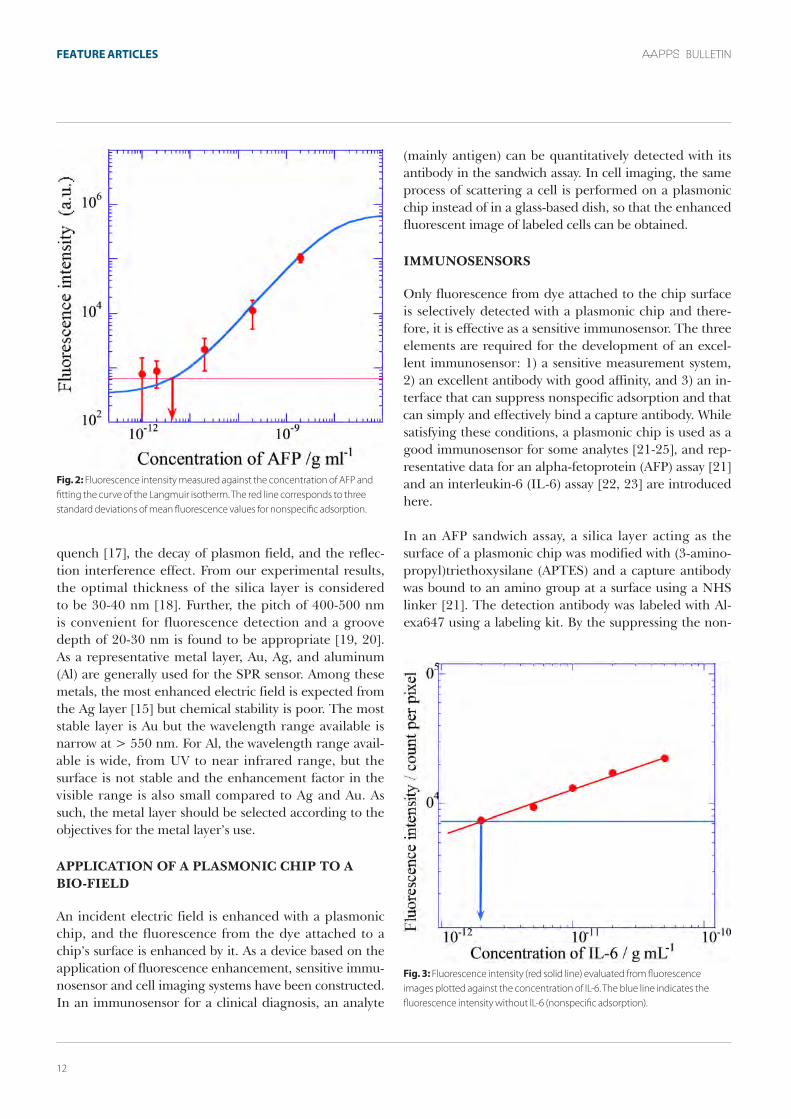
fig. 2: Fluorescence intensity measured against the concentration of AFP and fitting the curve of the Langmuir isotherm. The red line corresponds to three standard deviations of mean fluorescence values for nonspecific adsorption.
fig. 3: Fluorescence intensity (red solid line) evaluated from fluorescence images plotted against the concentration of IL-6. The blue line indicates the fluorescence intensity without IL-6 (nonspecific adsorption).
13
JUNE 2019 VOL. 29 NO. 3 fEatUrE artiClEs
specific adsorption, in the silver plasmonic chip the limit of detection (LOD) was evaluated as 4pg/mL (55 fM) as shown in Fig. 2. In order to improve the LOD, the stabil-ity of optics including incident light intensity and the reproducibility of a plasmonic chip structure should be considered.
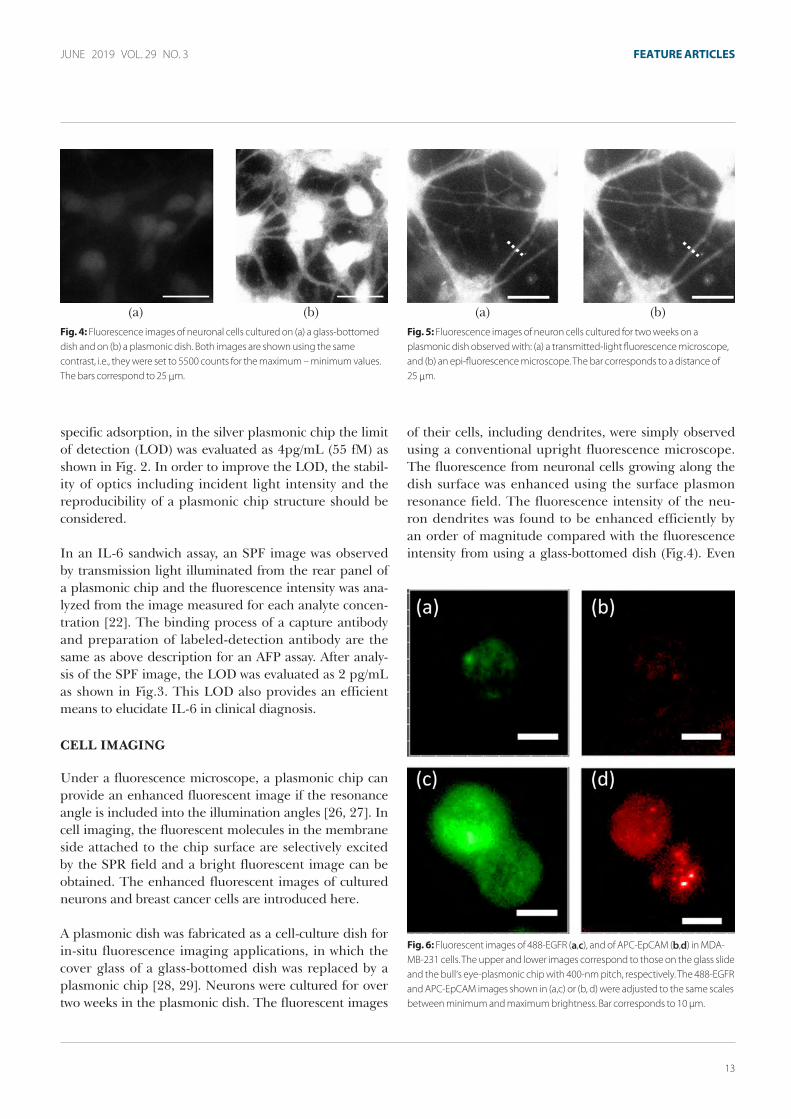
In an IL-6 sandwich assay, an SPF image was observed by transmission light illuminated from the rear panel of a plasmonic chip and the fluorescence intensity was ana-lyzed from the image measured for each analyte concen-tration [22]. The binding process of a capture antibody and preparation of labeled-detection antibody are the same as above description for an AFP assay. After analy-sis of the SPF image, the LOD was evaluated as 2 pg/mL as shown in Fig.3. This LOD also provides an efficient means to elucidate IL-6 in clinical diagnosis.
CELL IMAGING
Under a fluorescence microscope, a plasmonic chip can provide an enhanced fluorescent image if the resonance angle is included into the illumination angles [26, 27]. In cell imaging, the fluorescent molecules in the membrane side attached to the chip surface are selectively excited by the SPR field and a bright fluorescent image can be obtained. The enhanced fluorescent images of cultured neurons and breast cancer cells are introduced here.
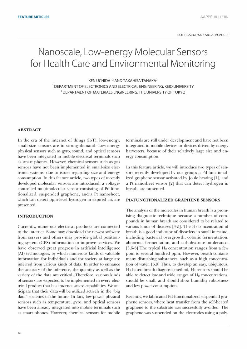
A plasmonic dish was fabricated as a cell-culture dish for in-situ fluorescence imaging applications, in which the cover glass of a glass-bottomed dish was replaced by a plasmonic chip [28, 29]. Neurons were cultured for over two weeks in the plasmonic dish. The fluorescent images
of their cells, including dendrites, were simply observed using a conventional upright fluorescence microscope. The fluorescence from neuronal cells growing along the dish surface was enhanced using the surface plasmon resonance field. The fluorescence intensity of the neu-ron dendrites was found to be enhanced efficiently by an order of magnitude compared with the fluorescence intensity from using a glass-bottomed dish (Fig.4). Even
fig. 6: Fluorescent images of 488-EGFR (a,c), and of APC-EpCAM (b,d) in MDA-MB-231 cells. The upper and lower images correspond to those on the glass slide and the bull’s eye-plasmonic chip with 400-nm pitch, respectively. The 488-EGFR and APC-EpCAM images shown in (a,c) or (b, d) were adjusted to the same scales between minimum and maximum brightness. Bar corresponds to 10 µm.
fig. 4: Fluorescence images of neuronal cells cultured on (a) a glass-bottomed dish and on (b) a plasmonic dish. Both images are shown using the same contrast, i.e., they were set to 5500 counts for the maximum – minimum values. The bars correspond to 25 μm.
fig. 5: Fluorescence images of neuron cells cultured for two weeks on a plasmonic dish observed with: (a) a transmitted-light fluorescence microscope, and (b) an epi-fluorescence microscope. The bar corresponds to a distance of 25 μm.
(a) (b) (a) (b)

14
BULLETINfEatUrE artiClEs
if the culture term is short, the neuron dendrites were clearly observed. Furthermore, in a transmitted-light fluorescence microscope, the surface-selective fluorescent image of a fine dendrite growing along the dish surface was observed with a high spatial resolution (Fig. 5).
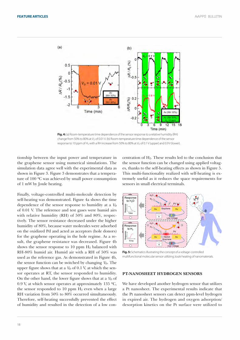
In breast cancer cell observations [30, 31], the epithelial cell adhesion molecule (EpCAM) and the epidermal growth factor receptor (EGFR) were observed in the Michigan cancer foundation-7 (MCF-7) and MDA-MB-231 using a plasmonic chip, i.e., the surface plasmon field-enhanced fluorescence. Expression level of EpCAM in MCF-7 cells is generally known to be more than that in MDA-MB-231. In our first study of breast cancer cells, EpCAM was labelled with an allophycocyanin-labeled anti-EpCAM antibody (APC-EpCAM), and the brighter fluorescent images of MCF-7 and MDA-MB-231 cells were obtained on the plasmonic chip with 480-nm pitch compared with those on the glass slide [30]. In the second study, these membrane proteins, EpCAM and EGFR, that acted as the surface markers used to dif-ferentiate breast cancer cells were then detected with the dye Alexa 488 - labeled anti-EGFR antibody (488-EGFR) and APC-EpCAM, respectively [31]. For the MDA-MB231 cells, 3-fold and 7-fold fluorescence enhance-ment in 488-EGFR were observed on the bull’s eye-type plasmonic chip with 480-nm pitch and the 400-nm pitch (Fig. 6 (c)), respectively (compared with the fluorescence intensities on a glass slide). On the other hand, 9-fold fluorescence intensity in APC-EpCAM was obtained on a 400-nm pitch plasmonic chip (Fig. 6(b) and (d)). So, dual-color fluorescence of 488-EGFR and APC-EpCAM in MDA-MB231 was clearly observed on the plasmonic chip with a 400-nm pitch as shown in Fig. 6. Fluores-cence enhancement with a plasmonic chip depends on the wavelength. The surface plasmon coupling at the 400-nm pitch contributed to the enhancement of the excitation field for APC-EpCAM and to the collection of the surface plasmon-coupled emission (SPCE) for 488-EGFR effectively under the microscope. Therefore, the 400-nm pitch contributed to the dual-color fluorescence enhancement for these wavelength ranges.
CONCLUSION
The structure and mechanism of a plasmonic chip in providing enhanced fluorescence is explained and the application of plasmonic chips to immunosensor and cell imaging is introduced. The plasmonic chip is an excellent and simple tool for the sensitive detection of
analytes, but sensor interface suppressing non-specific interaction and densely binding capture antibodies are required for more effective biodetection. With the im-provement of the sensor interface, further sensitive de-tection can be implemented. On the other hand, in the fluorescent images of cells, the fluorescent molecules ex-isting in the membrane side attached to the chip surface, i.e., the fluorescent molecules located within 200-nm distance from the surface, are selectively excited by SPR field and a bright fluorescent image can be obtained. Distribution of EpCAM and EGFR into cells is clearly ob-served on the plasmonic chip with an appropriate pitch; this distribution cannot be observed on a glass slide. The enhancement of fluorescence using a plasmonic chip is useful to detect small signals, and further applications of plasmonic chips are expected to be discovered in other fields.
Acknowledgements: I thank Prof. Dr. J. Nishii, Prof. Dr. XQ. Cui, Dr. K. Kintaka, Dr. S. Yamamura, Prof. Dr. C. Hosokawa, and Dr. T. Kaya, for their respective collabo-rations and discussions. I also thank C. Yasui, F. Kondo, M. Tsuneyasu, and S. Izumi for performing experiments and analyzing data. I thank Toyo Gosei for providing the UV-curable resin PAK-02-A. This work was supported by JSPS KAKENHI Grant Numbers 19049016 on Priority Area “Strong Photons-Molecules Coupling Fields (No. 470)”, JP15H0110 in Scientific Research on Innovation Areas “Photosynergetics”, 25286032 in Scientific Re-search (B), and JP16H02092 in Scientific Research (A).
References
[1] L. nieba, A. Krebber, and A. Pluckthun: Anal. biochem. 234, 155 (1996).[2] L. nieba, S. e. niebaAxmann, A. Persson, M. hamalainen, f. edebratt, A.
hansson, J. Lidholm, K. Magnusson, A.f. Karlsson, and A. Pluckthun: Anal. biochem. 252, 217 (1997).
[3] P. Mulvaney: Langmuir 12, 788 (1996).[4] b. nikoobakht and M. A. el-Sayed: chemistry of Materials 15, 1957 (2003).[5] K. A. willets and r. P. Van duyne: Annu. rev. Phys. chem. 58, 267 (2007).[6] c. L. haynes and r. P. Van duyne: J. Phys. chem. b 105, 5599 (2001).[7] e. hao and g. c. Schatz: J. chem. Phys. 120, 357 (2004).[8] J. homola, S. S. Yee, and g. gauglitz: Sensors and Actuators b: chemical 54,
3 (1999).[9] e. engvall and P. Perlmann: Immunochemistry 8, 871 (1971).[10] T. Liebermann and w. Knoll: colloids Surf. A 171, 115 (2000).[11] f. Yu, d. Yao, and w. Knoll: Anal. chem. 75, 2610 (2003).[12] h. räther: Surface Plasmons on Smooth and rough Surfaces on gratings
(Springer-Verlag, 1988).[13] w. Knoll: Annu. rev. Phys. chem. 49, 569 (1998).[14] I. gryczynski, J. Malicka, Z. gryczynski, and J. r. Lakowicz: J. Phys. chem. b
108, 12568 (2004).

15
JUNE 2019 VOL. 29 NO. 3 fEatUrE artiClEs
Keiko tawa is a professor at the School of Science and Technology, Kwansei Gakuin University, Japan. She received her PhD in engineering from Kyoto University, Japan in 1995. Her research interests are spectroscopy and plasmonics, specifically in the field of nano-biophysics including sensor and optical imaging of cells and proteins.
[15] K. Tawa, Y. Yokota, K. Kintaka, J. nishii, and T. nakaoki: Sens. Act. b: chemical 157, 703 (2011).
[16] K. Tawa and K. Morigaki: biophysical J. 89, 2750 (2005).[17] r. r. chance, A. Prock, and r. Silbey: Adv. chem. Phys. 37, 1 (1978).[18] K. Tawa, T. nakayama, and K. Kintaka: Materials, 10, 1063 (2017).[19] X. Q. cui, K. Tawa, h. hori, and J. nishii: Adv. funct. Mater. 20, 546 (2010).[20] X. Q. cui, K. Tawa, K. Kintaka, and J. nishii: Adv. funct. Mater. 20, 945 (2010).[21] K. Tawa, f. Kondo, c. Sasakawa, K. nagae, Y. nakamura, A. nozaki, and T.
Kaya: Anal. chem. 87, 3871(2015). [22] M. Tsuneyasu, c. Sasakawa,n. naruishi, Y. Tanaka, Y. Yoshida, K. Tawa: Jpn. J.
Appl. Phys. 53, 06JL05 (2014). [23] M. Toma, K. Tawa: AcS Appl. Mater. & Interfaces 8, 22032 (2016).[24] r. Matsuura, K. Tawa, Y. Kitayama, and T. Takeuchi: chem. commun. 52,
3883 (2016).
[25] M. Toma, S. Izumi, and K. Tawa*, Analyst, 143, 858 (2018). [26] K. Tawa, h. hori, K. Kintaka, K. Kiyosue, Y. Tatsu, and J. nishii: opt. express
16, 9781 (2008).[27] K. Tawa, S. Izumi, c.Sasakawa, M. Toma, and c. hosokawa: opt. express 25,
10622 (2017).[28] K. Tawa, c.Yasui, c. hosokawa, h. Aota, and J. nishii: AcS Appl. Mater.
Interfaces, 6, 20010 (2014). [29] K. Tawa*, c. Sasakawa, T. fujita, K. Kiyosue, c. hosokawa, J. nishii, M. oike,
and n. Kakinuma, Jpn. J. Appl. Phys., 55, 03df12, (2016).[30] K. Tawa, S. Yamamura, c. Sasakawa, I. Shibata, and M. Kataoka: AcS Appl.
Mater. Interfaces 8, 29893 (2016).[31] S. Izumi, n. hayashi, S. Yamamura, M. Toma, and K. Tawa*, Sensors, 17,
2942 (2017).
16
BULLETINfEatUrE artiClEs
ABSTRACT
In the era of the internet of things (IoT), low-energy, small-size sensors are in strong demand. Low-energy physical sensors such as gyro, sound, and optical sensors have been integrated in mobile electrical terminals such as smart phones. However, chemical sensors such as gas sensors have not been implemented in small-size elec-tronic systems, due to issues regarding size and energy consumption. In this feature article, two types of recently developed molecular sensors are introduced; a voltage-controlled multimolecular sensor consisting of Pd-func-tionalized, suspended graphene, and a Pt nanosheet, which can detect ppm-level hydrogen in expired air, are presented.
INTRODUCTION
Currently, numerous electrical products are connected to the internet. Some may download the newest software from servers and others may provide global position-ing system (GPS) information to improve services. We have observed great progress in artificial intelligence (AI) technologies, by which numerous kinds of valuable information for individuals and for society at large are inferred from various kinds of data. In order to enhance the accuracy of the inference, the quantity as well as the variety of the data are critical. Therefore, various kinds of sensors are expected to be implemented in every elec-trical product that has internet access capabilities. We an-ticipate that their data will be utilized actively in the “big data” societies of the future. In fact, low-power physical sensors such as temperature, gyro, and optical sensors have been already integrated into mobile terminals such as smart phones. However, chemical sensors for mobile
terminals are still under development and have not been integrated in mobile devices or devices driven by energy harvesters, because of their relatively large size and en-ergy consumption.
In this feature article, we will introduce two types of sen-sors recently developed by our group; a Pd-functional-ized graphene sensor activated by Joule heating [1], and a Pt nanosheet sensor [2] that can detect hydrogen in breath, are presented.
PD-FUNCTIONALIZED GRAPHENE SENSORS
The analysis of the molecules in human breath is a prom-ising diagnostic technique because a number of com-pounds in human breath are considered to be related to various kinds of diseases [3-5]. The H2 concentration of breath is a good indicator of disorders in small intestine, including bacterial overgrowth, colonic fermentation, abnormal fermentation, and carbohydrate intolerance. [3,6-8] The typical H2 concentration ranges from a few ppm to several hundred ppm. However, breath contains many disturbing substances, such as a high concentra-tion of water. [6,9] Thus, to develop an easy, ubiquitous, H2-based breath diagnosis method, H2 sensors should be able to detect low and wide ranges of H2 concentrations, should be small, and should show humidity robustness and low power consumption.
Recently, we fabricated Pd-functionalized suspended gra-phene sensors, where heat transfer from the self-heated graphene to the substrate was successfully avoided. The graphene was suspended on the electrodes using a poly-
Nanoscale, Low-energy Molecular Sensorsfor Health Care and Environmental Monitoring
Ken UchIdA1,2 And TAKAhISA TAnAKA2 1 dePArTMenT of eLecTronIcS And eLecTrIcAL engIneerIng, KeIo UnIVerSITY
2 dePArTMenT of MATerIALS engIneerIng, The UnIVerSITY of ToKYo
doI: 10.22661/AAPPSbL.2019.29.3.16

17
JUNE 2019 VOL. 29 NO. 3 fEatUrE artiClEs
dimethylsiloxane (PDMS) stamp method. [10,11] By uti-lizing Joule heating within the suspended graphene, we explored the possibility of selective sensing of hydrogen/humidity by applying an appropriate bias voltage in real-istic gas environments, in which small changes in the H2 concentration and large variations in the relative humid-ity (RH) were induced.
Figure 1 shows the fabricated Pd-functionalized gra-phene sensor. The 300-nm-thick SiO2 thermally grown on the p-type Si substrate was used as the substrate. After the formation of Ti/Pt/Au electrodes on SiO2, HOPG was exfoliated using Nitto tape (SPV224-R) and placed on commercially available PDMS (Gel-Film® WF-20×4 6mil). The PDMS was used to transfer the graphene on the electrodes. The graphene was transferred by a PDMS stamping method. After cleaning, 0.3-nm-thick Pd was deposited and agglomerated by annealing at 400 °C for 30 min. The suspension was confirmed by scanning elec-tron microscopy (SEM) and the multi-layer structure and high quality of suspended graphene was checked by Ra-man spectroscopy. In addition, using transmission elec-tron microscopy (TEM), we confirmed that Pd was placed on graphene as nanoparticles (NPs) and that there were eight graphene layers. One might consider eight-layer graphene to be too thick to work with as a transducer. However, it is reported that the electrical conductivity of eight-layer graphene can be well modulated by external electric fields. [12] Therefore, eight-layer graphene can work as a transducer of hydrogen-induced changes.
Figure 2a shows the sensor response, which is defined by the resistance change (ΔR) relative to the original resistance (R0), to 100-ppm H2 as a function of time at
various operating temperatures from room temperature (RT) to 180 °C. The sensor response increases as the op-erating temperature increases to 135 °C, due to the pro-moted dissociative adsorption of H2. However, the sensor response decreases at 180 °C because of the desorption of hydrogen from Pd. Figure 2b shows the time depen-dence of the sensor response to 100-ppm H2, where the device was operated at various VD from 0.01 V to 1.1 V at RT. The sensor response increases as VD increases to 0.8 V, and then gradually decreases as VD continues to increase from 0.9 V to 1.1 V. This tendency of the VD-dependent sensor response is almost the same as that of the temper-ature-dependent sensor response, which clearly suggests that VD-induced self-heating was successfully achieved. To calibrate the graphene channel temperature when the self-heating technique was utilized, the sensor responses to 100 ppm of H2 using the self-heating technique and hot chuck were compared. We also verified the rela-
fig. 2: (a) Temperature dependence of the sensor response. The device was heated by an external heater. (b) Sensor response as a function of time at various drain voltages.
fig. 3: Temperatures as a function of self-heating power. Experimental temperatures were extracted by comparing VD-dependent and temperature-dependent sensor responses. Simulation data were obtained using multi-physics finite element method simulator with graphene-gold thermal contact resistance of 2500 μm2 · K/mW.
fig. 1: Schematic of fabricated Pd-functionalized graphene sensor. The graphene was suspended over two electrodes; one is a source that is grounded and the other is a drain that is biased with drain voltage (VD).
18
BULLETINfEatUrE artiClEs
tionship between the input power and temperature in the graphene sensor using numerical simulations. The simulation data agree well with the experimental data as shown in Figure 3. Figure 3 demonstrates that a tempera-ture of 100 °C was achieved by small power consumption of 1 mW by Joule heating.
Finally, voltage-controlled multi-molecule detection by self-heating was demonstrated. Figure 4a shows the time dependence of the sensor response to humidity at a VD of 0.01 V. The reference and test gases were humid airs with relative humidity (RH) of 50% and 80%, respec-tively. The sensor resistance decreased under the higher humidity of 80%, because water molecules were adsorbed on the oxidized Pd and acted as acceptors (hole donors) for the graphene operating in the hole regime. As a re-sult, the graphene resistance was decreased. Figure 4b shows the sensor response to 10 ppm H2 balanced with RH-80% humid air. Humid air with a RH of 50% was used as the reference gas. As demonstrated in Figure 4b, the sensor function can be switched by changing VD. The upper figure shows that at a VD of 0.1 V, at which the sen-sor operates at RT, the sensor responded to humidity. On the other hand, the lower figure shows that at a VD of 0.9 V, at which sensor operates at approximately 135 °C, the sensor responded to 10 ppm H2 even when a large RH variation from 50% to 80% occurred simultaneously. Therefore, self-heating successfully prevented the effect of humidity and resulted in the detection of a low con-
centration of H2. These results led to the conclusion that the sensor function can be changed using applied voltag-es, thanks to the self-heating effects as shown in Figure 5. This multi-functionality realized with self-heating is ex-tremely useful as it reduces the space requirements for sensors in small electrical terminals.
fig. 5: Schematics illustrating the concept of a voltage-controlled multifunctional molecular sensor utilizing Joule heating of nanomaterials.
PT-NANOSHEET HYDROGEN SENSORS
We have developed another hydrogen sensor that utilizes a Pt nanosheet. The experimental results indicate that the Pt nanosheet sensors can detect ppm-level hydrogen in expired air. The hydrogen and oxygen adsorption/desorption kinetics on the Pt surface were utilized to
fig. 4: (a) Room-temperature time dependence of the sensor response to a relative humidity (RH) change from 50% to 80% at VD of 0.01 V. (b) Room-temperature time dependence of the sensor response to 10 ppm of H2 with a RH increase from 50% to 80% at VD of 0.1 V (upper) and 0.9 V (lower).

19
JUNE 2019 VOL. 29 NO. 3 fEatUrE artiClEs
quantitatively model the sensor response of the Pt nano-sheets, based on the surface hydrogen coverage ratio.
Pt nanosheets were deposited using the electron beam deposition method on Si substrates covered with a 300-nm-thick SiO2 layer on the top. Aluminum electrode formation followed. Figure 6a shows the schematic of the sensor structure. Figure 6b shows the sectional TEM image of the Pt nanosheets. Polycrystalline Pt films with cracks were observed.
The sensor response, which is defined by the electri-cal current change (ΔI) relative to the original electrical current (I0), of a Pt nanosheet was found to be robust against humidity, as shown in Figure 7a. The substrate was heated at 150 °C. Compared to these Pt nanosheets, Pd nanosheets are much less robust as hydrogen sensors. For hydrogen concentrations from 500 ppb to 200 ppm, the response of the Pt nanosheet sensor was measured at RH = 0%, 50% and 90%. The same linear sensor re-sponse as a function of hydrogen concentration was obtained as shown in Figure 7b. Since room air typically contains 550 ppb hydrogen [13], expired air contains more hydrogen than typically in the atmosphere. Thus, the response of the Pt nanosheets tested here indicates
sensor response sufficient for hydrogen detection in ex-pired air. Furthermore, sensor response under expired air is shown in Figure 7c. Apparent increases of the sensor re-sponse just after the lunch as well as seven hours after the lunch were observed. These increases of sensor response are correlated with increases of hydrogen after ingesting foods; it is known that hydrogen concentrations inc.rease approximately six hours later when food is taken by ex-aminees [14,15]. Therefore, this experiment clearly dem-onstrates that the present Pt nanosheet sensor responded to low-level hydrogen in air expired by a healthy human.
fig. 8: Comparison of sensor response as a function of time between experimental data (symbols) and simulated data (lines).
We simulated the dependence of the sensor response on hydrogen concentration and time, by taking into account the time-dependent molecular coverage change [2]. The time-dependent sensor response at a hydrogen concen-tration of lower than 20 ppm was successfully reproduced by our model, as shown in Figure 8. However, at higher hydrogen concentrations, the calculated time depen-dence slightly deviates from the experimental data. We consider that the deviation was caused by catalytic water formation, which is not taken into account in our pres-
fig. 7: (a) Sensor response of the Pt nanosheet. (b) Hydrogen concentration dependence of the sensor response. (c) Time dependence of the sensor response to expired air.
fig. 6: (a) Schematics of Pt nanosheet sensor. (b) Cross-sectional transmission electron microscopy (TEM) image of a Pt nanosheet.
20
BULLETINfEatUrE artiClEs
ent model, on the Pt surface. At a hydrogen concentra-tion of less than 20 ppm, the surface coverage change is dominated by oxygen desorption. Therefore, the sensor response is precisely predicted by adsorption and des-orption of hydrogen and oxygen, which are fully consid-ered in the model. The robustness against humidity in hydrogen sensing is attributed to the small contribution of water to the hydrogen surface coverage.
CONCLUSION
In this article, two types of molecular sensors that we re-cently developed were introduced; a voltage-controlled multimolecular sensor consisting of Pd-functionalized, suspended graphene, and a Pt nanosheet that can detect ppm-level hydrogen in expired air were presented. In the Pd-functionalized, suspended graphene sensor, Joule heating is successfully utilized as a low-energy activator of chemical reactions. Although the Pt nanosheet sensor introduced in this article was heated up by an external heater, the same Joule heating method should be ap-plicable to lower the energy consumption of sensors. We believe that these small-size, low-energy sensors will become extremely useful in the “big data” societies of the future.
References [1] Yokoyama, T; Tanaka, T; Shimokawa, Y; Yamachi, r; Saito, Y, Uchida, K.
“Pd-functionalized, Suspended graphene nanosheet for fast, Low-energy Multimolecular Sensors,” AcS Applied nano Mat. 2018, 1, 3886-3894.
[2] Tanaka, T; hoshino, S; Takahashi, T; Uchida, K, “nanoscale Pt thin film sensor for accurate detection of ppm level hydrogen in air at high humidity,” Sensors and Actuators b chemical 2018, 258, 913-919.
[3] newcomer, A. d.; Mcgill. d. b; Thomas, P. J; hofmann, A. f. “Prospective comparison of Indirect Methods for detecting Lactase deficiency,” n. engl. J. Med. 1975, 293, 1232–1236.
[4] fuchs, P.; Loeseken, c.; Schubert, J. K.; Miekisch, w., “breath gas Aldehydes as biomarkers of Lung cancer,” Int. J. cancer 2010, 126, 2663–2670.
[5] filipiak, w.; ruzsanyi, V.; Mochalski, P.; filipiak, A.; bajtarevic, A.; Ager, c.; denz, h.; hilbe, w.; Jamnig, h.; hackl, M.; et al., “dependence of exhaled breath composition on exogenous factors, Smoking habits and exposure to Air Pollutants,” J. breath res. 2012, 6, 36008.
[6] Shin, w., “Medical Applications of breath hydrogen Measurements,” Anal. bioanal. chem. 2014, 406, 3931–3939.
[7] dewit, o.; Pochart, P.; desjeux, J.-f., “breath hydrogen concentration and Plasma glucose, Insulin and free fatty Acid Levels after Lactose, Milk, fresh or heated Yogurt Ingestion by healthy Young Adults with or without Lactose Malabsorption,” nutrition 1988, 4, 131–136.
[8] ghoshal, U. c., “how to Interpret hydrogen breath Tests,” J. neurogastroenterol. Motil. 2011, 17, 312–317.
[9] Mogera, U; Sagade, A. A.; george, S. J.; Kulkarni, g. U., “Ultrafast response humidity sensor using supramolecular nanofibre and its application in monitoring breath humidity and flow,” Sci. rep 2014, 4, 4103.
[10] Xia, Y. n.; whitesides, g. M., “Soft Lithography,” Annu. rev. Mater. Sci. 1998, 37, 551–575.
[11] whitesides, g. M.; ostuni, e.; Jiang, X.; Ingber, d. e., “Soft Lithography in biology and biochemistry,” Annu. rev. biomed. eng. 2001, 3, 335–373.
[12] nagashio, K.; nishimura, T.; Kita, K.; Toriumi, “A. Mobility Variations in Mono- and Multi-Layer graphene films,” Appl. Phys. express 2009, 2, 025003.
[13] Schmidt, U., “Molecular hydrogen in the atmosphere,” Tellus. 1974, 26, 78–90.
[14] nishibori, M; Shin, w.; Izu, n; Itoh, T; Matsubara, I. “Sensing performance of thermoelectric hydrogen sensor for breath hydrogen analysis,” Sensors Actuators b chem. 2009, 137, 524–528.
[15] Kondo, T; Liu, f; Toda, Y, “Milk is a useful test meal for measurement of small bowel transit time,” J. gastroenterol. 1994, 29, 715–720.
takahisa tanaka is a research associate at the School of Engineering, The University of Tokyo. He received his bachelor’s, master’s and doctorate degrees in engineering from Keio University in 2010, 2012 and 2015, respectively. His current area of research interest is the characterization of nanostructured materials applied to LSI and sensors.
Ken Uchida is a professor at the School of Engineering, The University of Tokyo. He received his B.S., M.S. and PhD degrees from The University of Tokyo in 1993, 1995, and 2002, respectively. He has studied carrier and thermal transports in nanoscaled materials and has developed advanced transistors and molecular sensors.

21
JUNE 2019 VOL. 29 NO. 3 fEatUrE artiClEs
ABSTRACT
This is a brief report on the present status and perspec-tives of the research programs with negative muon beams. Intense negative muon beams provide new research opportunities for neutrino nuclear responses and nuclear isotope detection and their production. We started the program at the Research Center for Nuclear Physics (RCNP), Osaka University, and now it is continu-ing at RCNP, J-PARC and the Paul Scherrer Institute (PSI). Gamma rays following ordinary muon capture reactions are used for studies of nuclear responses for anti-neutrinos associated with double beta decays and astro-neutrinos, and for high-sensitivity nuclear-isotope detection and high-efficiency nuclear-isotope produc-tion. Recently, we have started a new research project for these subjects in collaboration with Universiti Teknologi Malaysia (UTM) Johor Bahru, RCNP Osaka and the Joint Institute for Nuclear Research (JINR) Dubna. We discuss briefly recent results and perspectives regarding the muon experiments.
Keywords: Ordinary muon capture, neutrino nuclear responses, nuclear-isotope detection, nuclear isotope production.
INTRODUCTION
Muon beam experiments using negative muons are an alternative route for neutrino response studies, nuclear isotope detection and nuclear radioisotope production. Muon capture is a semi-leptonic reaction where a proton transforms into a neutron and a muon neutrino is emit-ted by the exchange of charged current (CC) weak W ± boson. It is given as
(1)
Muon capture is an extension of an electron capture re-action where one able to probe more available excited states up to J± = 4± states. When muon capture occurs, the target nucleus is excited to about 100 MeV in energy and most of the energy is carried away by the muon neutrino. The remaining energy can be absorbed by the nucleus and starts many other cascade reactions. From reference [1], the capture in light nuclei produces the emission of neutrons, protons and alpha particles. How-ever, for medium and heavy nuclei, neutrons are mainly emitted, with a very low possibility of proton and alpha emission due to the Coulomb barrier. These products have been observed through various experiments using neutron detectors and high-purity germanium (HPGe) detectors as discussed in the review paper and references therein [1].
The excitation region of the nuclei after muon capture corresponds to the neutrino nuclear response where the strength distributions of muon capture is observed. The neutrino nuclear response is important for studies of neutrino fundamental properties beyond the standard model. The neutrino response is crucial for neutrino studies by double beta decays (DBDs) [2-5]. Experimen-tal data of single beta (β– or β+) decay (SBD), inverse beta decay (IBD) and electron capture (EC) are well-estab-lished probes for current works due to their sensitivity for nuclear weak coupling constants gA and gV. The analysis of SBD, IBD and EC is much simpler when compared to the two-stage process of DBD, which involves transforma-tion from the parent to daughter nucleus through an in-termediate nucleus [2]. Furthermore, nuclear structures associated with DBDs are quite complicated since DBDs
New Research Project with Muon Beams for Neutrino Nuclear Responses and Nuclear
Isotopes ProductionhAShIM, I. h.1 And eJIrI, h.2
1 dePArTMenT of PhYSIcS, fAcULTY of ScIence, UnIVerSITI TeKnoLogI MALAYSIA, 81310 Johor bAhrU. 2 reSeArch cenTer of nUcLeAr PhYSIcS, oSAKA UnIVerSITY, SUITA-ShI 560-0067 oSAKA.
doI: 10.22661/AAPPSbL.2019.29.3.21

22
BULLETINfEatUrE artiClEs
include many multipole transitions in wide energy and momentum regions. All SBD, IBD, EC and DBD experi-ments investigate different areas of interest, where each respective area has important information for nuclear structure studies [3].
Various isotope production methods have been explored to detect nuclear isotopes with high sensitivity and to ef-ficiently produce specific radioisotopes (RIs), especially for environmental and biomedical applications. Neutron-induced reactions have been extensively used for RI pro-duction due to the large neutron flux available at nuclear reactors. The typical reaction is the neutron capture (n,γ) reaction. Recently, the photon capture reaction has been shown to be very effective for selectively producing RIs. The reaction used is the (γ,xn) reaction with x being 1 or 2, depending on the photon energy. Here, the cross sec-tion is large at the E1 giant resonance region, and high-flux photons are available by Compton back scattering of laser photons scattered off GeV electrons in a storage ring. RIs produced from the target isotope Z
AX are mainly ZA+1X and Z
A–1X, respectively, in the case of neutron cap-ture and photon capture reactions. They are RIs with dif-ferent mass numbers but with the same atomic number as the target isotope. On the other hand, muon capture reactions provide mainly nuclear isotopes with an atomic number of Z–1.
NEUTRINO NUCLEAR RESPONSES BY ORDINARY MUON CAPTURE REACTION
The study of neutrino nuclear response by ordinary muon capture (OMC) focuses on the β+ side response of double beta decay (DBD) and the astro anti-neutrino re-sponse [2, 6]. OMC excites the nucleus up to 100 MeV in the excitation range. Allowed, first forbidden and second forbidden β-multipoles are excited, as shown in Figure 1. The strength functions B(μ,E) are very sensitive to nucle-onic and non-nucleonic correlations [4]. The large ener-gy and momentum regions are similar to those involved in neutrino-less DBDs [2, 7-9]. Our recent work focuses on the neutrino nuclear responses for medium heavy nuclei. First, we used 100Mo as a target due to its being a familiar candidate for supernova neutrino experiments. The study of Mo DBD responses is under way, using a 100Ru target.
Investigations of OMC have been performed in a limited manner for stable and unstable nuclei and it will be a major undertaking to extend the investigations to neu-
trino nuclear response studies. Possibilities for realizing this goal are being investigated at the moment [9-11]. In the previous works, βγ-rays following such OMC RIs are shown to be very useful for studying DBD responses [2-5, 9, 12, 13] and also for studying fine nuclear isotopes of pure and applied science interests [10]. For medium-heavy nuclei, OMC is followed mainly (95%) by neutron emission with the remaining 5% coming from other par-ticle emissions such as proton emission [9, 10, 14-16].
In reference [9], the extensive study of muon strength distribution using OMC on 100Mo has been studied. The negative muon beam from the D2 beamline of the Material Life Science Facility (MLF) J-PARC was used to irradiate 100Mo (94.5% in enrichment). RIs produced af-ter the emission of up to 5 neutrons were observed. The total number of the stopped muons was around 108. The prompt and delayed γ-rays from RIs produced by (μ, xnν) reactions with x = 0, 1, …, 5 were measured by means of two Ge detectors. The irradiation of the target was made for 6.5 hours.
The prominent γ-ray peaks from Nb and Tc isotopes have been measured at 100Nb (535 keV), 99Nb (137keV), 99mTc: (140.5 keV, 181 keV and 735 keV), 98Nb: (722 keV and 787 keV), 97Nb: (658 keV) and 96Nb: (460 keV, 569keV and 778 keV) in the online and offline γ spectra. The peak yields undergo analysis to obtain the number of isotopes produced by (μ, xnν) reactions and thus RI
fig. 1: Ordinary muon capture (OMC) on 100Mo excites the target up to ~100 MeV in excitation energy by a charge exchange reaction given in eqn.(1). The excited state decays by multiple neutron and proton emissions are shown.

23
JUNE 2019 VOL. 29 NO. 3 fEatUrE artiClEs
mass distribution can be obtained. It shows that a (μ, ν) reaction with no neutrons is less probable compared to (μ, 1nν) and (μ, 2nν) reactions. The observed RI mass distribution for OMC on 100Mo is compared to the cal-culated mass distribution using the neutron emission model (NEM) to evaluate the strength distribution of the reactions. The obtained RI mass distribution is compared with the observed one in Figure 2(a).
The agreement with the observed data is quite good. Here, two giant resonance (GR) peaks EG1 and EG2 are observed at 12 MeV and 29 MeV (Fig. 2(b)) with an in-tensity ratio of EG1 / EG2 = 1/6. The OMC GR energy of 12 MeV is a bit smaller than the GR energy of 14 MeV for the photon capture reaction (PCR). The wider width of 8 MeV for the OMC GR is due to the mixed compo-nents of Jπ = 1–, 1+, 2–, 2+, ... while PCR GR (5 MeV) has only one component, Jπ = 1–.
The NEM was developed in 2014 [17] for the evaluation of relative capture strength from radioisotope production rates. Since then, various calculations have been made for understanding the formation of the giant resonance peak populated by muon capture reactions in 2<A<209 [18-21]. These calculations have been compared with previous experimental works by OMC on the nuclei re-ported in references [1, 11, 22]. From these observations, it can be noted that one neutron emission gives a major contribution of about 45% to 65% after muon capture. For lighter nuclei, the one neutron emission is greater than 50%. The mass distribution provides the relative capture strength of the reaction where captures on en-riched nuclei populates almost 95% of the RIs by neu-tron emission. Natural targets with a wide isotope mass
distribution can also be used for producing various re-sidual isotopes in a wider mass range where high chances of proton emission can be observed.
The NEM shows preferential excitation of the GR region with EG1 = 10 – 20 MeV in the nucleus X. The second GR is expected to reproduce the experimental data at peak around EG2 = 25 – 40 MeV. The strength distribu-tion of B(μ, E) is given by the sum of the two giant reso-nance strengths of B1(μ, E) and B2(μ, E) [2, 9]
(2)
(3)
where EGi and Γi with i=1,2 are the resonance energy and the width for the ith giant resonance, and the con-stant Bi(μ) is expressed as Bi(μ) = σiΓi/(2π) with σi being the total strength integrated over the excitation energy. The parameters of EG1 and EG2 as a function of A are giv-en as EG1 = 25A–1/5 and EG2 = 75A–1/5 for OMC on 23Na, 24Mg, 27Al, 28Si, 40Ca, 56Ni, 76Se, 100Mo, 106Cd, 127I, 150Sm, 197Au and 209Bi. They are obtained from a comparison of NEM calculations with experimental data. As a final remark, the GR distribution obtained by this comparison provides information of the relative capture strength.
Primakoff derived absolute muon capture rates [23]. The capture rate is expressed as
. (4)
From experimental data, Primakoff obtained X = 0.73
fig. 2: Output from a neutron emission model (NEM): (a) the comparison between calculated and experimental data from reference [9] and (b) the strength distribution to reproduces the RI mass distribution in (a).

24
BULLETINfEatUrE artiClEs
and X′ = 3. Later, total muon capture experiments [24] were performed at the M20 channel in TRIUMF for many light and heavy target nuclei, i.e., 12C, 18O H2O, LiF, CaF2, PbF, CCl4, Sc2O3, MnO2, GeO2, Br, I, BaO, NdO, W, and HgO. For all these nuclei, the impurities were less than l %. For heavy elements, higher order Pauli corrections become necessary and the equation (4) is modified as
. (5)
Together with their experimental data and calculations using equation (4) and (5), they reported the mean lives τ and the total capture rates Λc for isotope with 1<Z<94.
The partial capture rate measured by [11, 14-16, 22] is deduced from muon disappearance rate ΛT expressed by,
(6)
where ΛC = ΛC(0n)+ΛC(1n)+ΛC(2n)+ΛC(1p)+…, Λfree is the free muon decay rate (0.4552 × 10⁶ s–1) and H is the Huff factor from reference [24]. In the publication [11], the decay rates for natural Se, Kr, Cd and Sm and also enriched 48Ti, 76Se, 82Kr, 106Cd and 150Sm were observed by experiments at μE1 and μE4 beamlines at Paul Scher-rer Institute (PSI).
NUCLEAR ISOTOPE DETECTION AND PRODUCTION BY USING MUON CAPTURE REACTION
The present OMC is also used for a non-destructive high-sensitivity detection (assay) of nuclear isotopes. It is interesting for basic and applied science. The sensitivi-ties are of the orders of ppm–ppb by measuring nuclear gamma rays following muon capture reactions [10]. The feasibility test of this method was done at MuSIC, Osaka University in 2012 using NatMo targets. Low-energy nega-tive muons are stopped in a bulk sample, where each muon is trapped in one of the atoms and promptly emits muonic x-rays. Then the muon either decays to electron directly or is captured into the nucleus. The muon is likely to be captured into the nucleus unless the atomic number is smaller than Z =10. Muon capture isotope detection (MuCID) uses OMC nuclear reactions to trans-
mute isotopes X of interest to radioactive isotopes (RIs) X′ and the production of the X′ RIs is measured by ob-serving nuclear γ rays with high-sensitivity Ge detectors. The low background (BG) and high energy-resolution measurements of the characteristic γ rays are key points of the present high-sensitivity detection/assay method.
The resonant photonuclear isotope detection (RPID) method using photon-capture reactions has been shown to be very useful for nuclear isotope detection [25]. It has similar sensitivities as the present MuCID, but the radio-active isotopes produced by muon and photon capture reactions are very different. Accordingly, sample forms and nuclear isotopes to be studied by the present MuCID are different from those by RPID. Neutron activation analysis has extensively been used for high-sensitivity iso-tope assay. It, however, is used mainly for isotopes with a large neutron-capture cross section. On the other hand, muon capture probabilities are almost 100 % for all iso-topes with Z ≥ 10. Thus, MuCID is used for nuclei in a wide mass region if the reaction products are radioactive. The decay and capture scheme of MuCID, RPID and neutron activation is shown in Figure 3.
fig. 3: Decay scheme comparing MuCID, RPID and neutron activation reactions.
MuCID and RPID are summarized in Table 1. In a Mu-CID method, more RIs could be observed mostly coming from the X isotope where x = 0, 1, 2, ..., 5. In 100Mo [9] and NatMo [10], the total RI production rate is 95% and 43% respectively. Predominantly, the excited state with the excitation energy E in the A
Z–1X after the μ-capture (μ,νμ) reaction de-excites by emitting neutrons at the pre-equilibrium (PEQ) and equilibrium (EQ) stages [26] if the state is neutron unbound, and de-excite by emitting γ rays to the ground state if it is particle bound.
MuCID, RPID and neutron activation are complementa-ry to each other. They are often used to study rare and/or

25
JUNE 2019 VOL. 29 NO. 3 fEatUrE artiClEs
small components of nuclear isotopes, which are of great interest in astro-nuclear, particle and material sciences, geological and historical science and for other fields of science and technology, as shown in Table 1.
Muon capture isotope production (MuCIP) by using negative muon capture reaction can be used to provide efficiently various kinds of nuclear isotopes for studies of fundamental and applied science [27]. The large capture probability of a muon into a nucleus, together with the availability of a high intensity muon beam, makes it pos-sible to produce nuclear isotopes of the order of 106–9 per sec. Radioactive isotopes (RIs) produced by MuCIP are complementary to those by photon and neutron cap-ture reactions, and are used for various kinds of applica-tions in science and technology.
MuCIP on Mo, using the RCNP MuSIC muon beam, was made at RCNP to demonstrate the feasibility of MuCIP [27]. Radioactive 99Mo isotopes and meta-stable 99mTc isotopes, which are used extensively for medical science, were produced by MuCIP on 100Mo.
PERSPECTIvES ON MUON BEAM NUCLEAR PHYSICS
The present report discusses briefly (1) a new method to study the neutrino nuclear response relevant to astro-an-tineutrino interactions and DBDs by OMC and (2) a new method for isotope detection and production by OMC. μ – γ spectroscopy is reliable for studying the higher momentum-transfer responses of the intermediate nu-clei of DBDs in comparison with the lower momentum-transfer responses by electron capture. The neutron emissions following OMC on natural molybdenum and enriched molybdenum show that 1 neutron emission is the dominant process and 2 or 3 neutron emissions are appreciable. The statistical neutron emission model, with neutron emissions at the PEQ and EQ stages, is used to evaluate the muon-capture strength from the observed RI-mass distributions.
The characteristic delayed gamma rays following neu-tron and proton emissions have been well studied in order to evaluate the residual RI production rates. The dominant excitation by OMC is the muon giant reso-nance at a lower energy excitation of around 10 to 15 MeV. Some strength is located at around 20-30 MeV. The relative strength distribution, together with the muon capture lifetime, can be used to study the muon capture strengths, which are used to help determine the neutrino nuclear responses for astro-antineutrinos and DBDs.
Theoretical work on the 100Mo data [9] has recently been made using proton neutron quasi particle random phase approximation (pn-QRPA). The observed GR strength is well reproduced for the OMC on 100Mo. Neutrino nuclear responses calculated by pn-QRPA may be used to study weak coupling constants such as gA and gPP. [28].
A collaborative project involving three institutes-Univer-siti Teknologi Malaysia (UTM); the Research Center of Nuclear Physics (RCNP), Osaka University; and the Joint Institute for Nuclear Research (JINR), Russia – began in 2017. The collaboration aims to study the neutrino nuclear response by OMC through the observation of prompt and delayed gamma rays on various nuclei. The first joint program took place at the MuSIC facil-ity, RCNP, Osaka University on Feb 2018. The results on muon absolute lifetimes on 100Mo, NatMo, NatRu and NatSe are currently under progress.
table 1: Radioactive isotopes to be studied by MuCID (μ, xn) reactions and comments (examples) on RIs by RPID (γ, n) reactions. Half-lives are given by d: day or h: hour.
Isotope μ reaction RI (half life) Comments on (γ, n)
54Fe (μ, 2n) 52Mn (5.59 d) 53Fe: short life
56Fe (μ, 0n) 56Mn (2.58 h) 55Fe: no γ
65Cu (μ, 0n) 65Ni (2.5h) 64Cu: 12.7 h
90Zr (μ, 0n) 90Y (64.1 h) 89Zr: 78.4 h
92Zr (μ, 0n) 92Y (3.54 h) 91Zr: stable
99Tc (μ, 0n) 99Mo (65.9 h) 98Tc: long life
109Ag (μ, 0n) 109Pd (13.7 h) 108Ag: short / long life
128Te (μ, 1n) 127Sb (3.85 d) 127Te: 9.4 h, 109 d
187Re (μ, 0n) 187W (23.7 h) 186Re: 90.6 h
197Au (μ, 0n) 197Pt (18.3 h) 196Au: 6.18 d
233U (μ, 0n) 233Pa (27.0 d) 232U: long life
235U (μ, 1n) 234Pa (6.7 h) 234U: long life
239Pu (μ, 0n) 239Np (2.36 d) 238Pu: long life
240Pu (μ, 0n) 240Np (1.03 h) 239Pu: long life

26
BULLETINfEatUrE artiClEs
References
[1] d.f. Measday, Physics reports, 354 (2001) 243. [2] h. ejiri, J. Suhonen, K. Zuber and Physics reports 797 (2019) 1–102.[3] h. ejiri, J. Phys. Soc. Jpn. 74 (2005) 2101.[4] h. ejiri, Proc. cnnP2017, catania 2017, IoP conf. Series, 1056 (2018)
012019.[5] h. ejiri, Phys. rep. 338 (2000) 265.[6] h. ejiri, AIP conference Proceedings 1686 (2015) 020010.[7] h. ejiri. czech J. Phys. 56 5 (2006) 459.[8] h.o.U, fynbo et al. nuclear Physics A 724 (2003) 493.[9] I. hashim, h. ejiri, et al., Phys. rev. c 97 (2018) 014617. [10] h. ejiri, I. hashim, et al. J. Phys. Soc. Japan, 82 (2013) 044202.[11] d. Zinatulina et al. Phys. rev. c 99 (2019) 024327.[12] f. Avignone, S. elliott, and J. engel rev. Mod. Phys. (2008) 80481. [13] J. Vergados, h. ejiri, and f. Simkovic, rep. Prog. Phys. 75 (2012) 106301. [14] d.f. Measday, Phys. rev. c 76 (2007) 035504.[15] d.f. Measday, Phys. rev. c 75 (2007) 045501.
[16] d.f. Measday and T.J. Stocki, AIP conference Proceedings 947 (2007) 253.[17] I.h. hashim. Phd Thesis (2014). osaka University.[18] S.S. Saroni, Yw workshop MXg16, rcnP, osaka, Sep. 2016.[19] I.h. hashim et al, ePJ web of conferences, UTM, Johor 156 (2017) 00005.[20] n.f.h. Muslim, PSM Symposium Proceeding, UTM, Johor (2018) 100.[21] f. Ibrahim, PSM Symposium Proceeding, UTM, Johor (2018) 106.[22] V. egorov et al. czechoslovak Journal of Physics, 56 5 (2006) 453.[23] h. Primakoff, rev. Mod. Phys. 31 (1959) 802.[24] T. Suzuki, d.f. Measday and J.P roalsvig. Phys. rev. c 35 6 (1987) 2212.[25] h. ejiri and T. Shima Phys. rev. ST Accel. beams 15 (2012) 024701.[26] h. ejiri and M.J.A. deVoigt, gamma ray and electron spectroscopy in
nuclear physics (1989) oxford, oxford University Press.[27] I.h. hashim, h. ejiri et al. to be submitted 2019.[28] L. Jokiniemi, J. Suhonen, h. ejiri and I.h. hashim, submitted to Phys.
Letters b 2019.
hiro Ejiri is a research professor at the Research Center for Nuclear Physics (RCNP), Osaka University and an emeritus professor of Osaka University. He received his PhD in 1963 from the University of Tokyo. He has worked at the University of Tokyo, the University of Washington, the University of Copenhagen, the University of California and Osaka University. He is a former director of RCNP, Osaka University. His research fields include nuclear structures, nuclear reactions, hyper nuclear physics, neutrino nuclear physics, double beta decays, and dark matter.
izyan hazwani hashim is a senior lecturer at the Universiti Teknologi Malaysia, Johor Bahru and a research fellow of the National Centre Particle Physics, Universiti Malaya and visiting researcher at the Research Center for Nuclear Physics (RCNP), Osaka University. She received her PhD in physics from Osaka University, Japan in 2014. She is an experimental physicist with research interests in neutrino nuclear physics, double beta decays and muon physics.

27
JUNE 2019 VOL. 29 NO. 3 aCtiVitiEs and rEsEarCh nEWs
The experiment, which will complement existing searches for dark matter at the LHC, will be operational in 2021
Geneva. Today, the CERN Research Board approved a new experiment designed to look for light and weakly interacting particles at the LHC. FASER, or the Forward Search Experiment, will complement CERN’s ongoing physics programme, extending its discovery potential to several new particles. Some of these sought-after particles are associated with dark matter, which is a hypothesised kind of matter that does not interact with the electromag-netic force and consequently cannot be directly detected using emitted light. Astrophysical evidence shows that dark matter makes up about 27% of the universe, but it has never been observed and studied in a laboratory.
With an expanding interest in undiscovered particles, particularly long-lived particles and dark matter, new experiments have been proposed to expand the scientific potential of CERN’s accelerator complex and infrastruc-ture as part of the Physics Beyond Collider (PBC) study, under whose aegis FASER operates. “This novel experi-ment helps diversify the physics programme of colliders such as the LHC, and allows us to address unanswered questions in particle physics from a different perspec-tive,” explains Mike Lamont, co-coordinator of the PBC study group.
The four main LHC detectors are not suited for detect-ing the light and weakly interacting particles that might be produced parallel to the beam line. They may travel hundreds of metres without interacting with any material
FASER: CERN Approves New Experiment to Look for Long-lived, Exotic Particles
bY crISTInA AgrIgoroAe. PUbLIShed on 19 MArch 2019 In: MArch 2019, newS, cern, cern recognISed eXPerIMenT, eXoTIc PArTIcLeS, fASer,
Lhc eXPerIMenTS dArK MATTer
A 3D picture of the planned FASER detector as seen in the TI12 tunnel. The detector is precisely aligned with the collision axis in ATLAS, 480 m away from the collision point. (Image: FASER/CERN)
[reproduced from the e-ePS]

28
BULLETINaCtiVitiEs and rEsEarCh nEWs
before transforming into known and detectable particles, such as electrons and positrons. The exotic particles would escape the existing detectors along the current beam lines and remain undetected. FASER will there-fore be located along the beam trajectory 480 metres downstream from the interaction point within ATLAS. Although the protons in the particle beams will be bent by magnets around the LHC, the light, very weakly in-teracting particles will continue along a straight line and their “decay products” can be spotted by FASER. The potential new particles would be very collimated with the beam, spreading out very little, therefore allowing a rela-tively small and inexpensive detector to perform highly sensitive searches.
The detector’s total length is under 5 metres and its core cylindrical structure has a radius of 10 centimetres. It will be installed in a side tunnel along an unused transfer line which links the LHC to its injector, the Super Pro-ton Synchrotron. To allow FASER to be constructed in a quick and affordable way, it will use spare detector parts kindly donated from the ATLAS and LHCb experiments. The collaboration of 16 institutes that is building the de-
tector and will carry out the experiments is supported by the Heising-Simons Foundation and the Simons Founda-tion.
FASER will search for a suite of hypothesised particles including so-called “dark photons”, particles which are associated with dark matter, neutralinos and others. The experiment will be installed during the ongoing Long Shutdown 2 and start taking data from LHC’s Run 3 be-tween 2021 and 2023.
“It is very exciting to have FASER approved for installa-tion at CERN. It is amazing how the collaboration has come together so quickly and we are looking forward to recording our first data when the LHC starts up again in 2021,” says Jamie Boyd, co-spokesperson of the FASER experiment.
“FASER is a neat physics proposal that addresses a par-ticular aspect in the search for physics beyond the Stan-dard Model and I am pleased to see it being implement-ed so efficiently,” adds Eckhard Elsen, CERN’s Director for Research and Computing.

29
JUNE 2019 VOL. 29 NO. 3 institUtEs in asia PaCifiC
ADvANCED SCIENCE RESEARCH CENTER
The Advanced Science Research Center (ASRC) is a research center that is part of the Japan Atomic Energy Agency (JAEA), and focuses on the fundamental sciences related to atomic energy research and development. ASRC was established in April, 1993, in the former Japan Atomic Energy Research Institute (JAERI). When JAERI consolidated with the Japan Nuclear Cycle Development Institute in 2005 to become JAEA, the center continued operating without any constitutional changes. The aims of ASRC are (1) to focus on fundamental research per-taining to the origin of principles and phenomena, and to apply the results to atomic energy research and de-velopment, and (2) to conduct research that leads to the development of other fields along with the development of atomic energy. The center has been managed by di-rector generals, who, when they are chosen, are external to the ASRC’s present staff members. The foundation of the center was established by the first Director General Prof. Muneyuki DATE (Osaka Univ.), and Profs. Hiroshi YASUOKA (Univ. Tokyo), Yoshihiko HATANO (Tokyo Inst. Tech.), and Sadamichi MAEKAWA (Tohoku Univ.) have served as directors general in the 25 years that have passed since. Makoto OKA is the fifth director general, with Hidehito ASAOKA acting as the associate director since April 2018.
The center has seven research groups in FY2019, which cover heavy-element nuclear science, interfacial reaction field chemistry, hadron-nuclear physics, material science for heavy element systems, spin-energy transformation science, the nanoscale structure and function of advanced materials, and advanced theoretical physics. There are
presently about 75 current staff members, including the guest group leaders.
LOCATION AND FACILITIES
The location of the center (Fig. 1) is at the Tokai campus of JAEA, in Tokai village, Ibaraki prefecture of Japan. The campus has many large facilities devoted to nuclear science. Among them, the Japan Proton Accelerator Re-search Complex (J-PARC) is a high intensity proton ac-celerator complex operated jointly by JAEA and KEK. J-PARC is a multidisciplinary research facility that consists of a 400 MeV linear accelerator as the injector, a 3 GeV rapid-cycling synchrotron for multi-purpose neutron and
Advanced Science Research Center Japan Atomic Energy Agency
MAKoTo oKA And hIroYUKI KoUrA AdVAnced ScIence reSeArch cenTer, JAPAn AToMIc energY AgencY
fig. 1: The ASRC Building.

30
BULLETINinstitUtEs in asia PaCifiC
muon beam lines, and a 50 GeV (currently 30 GeV) main ring for secondary hadron beams (pion and kaon) as well as a neutrino beam for the long-baseline T2K experiment. The Tokai tandem accelerator, another nuclear physics facility, is a Van-de-Graaff type electro-static accelerator, which accelerates ions to a maximum voltage of 25 MV. The accelerator provides various species of ion beams, from hydrogen to bismuth on various radioactive target materials, including the actinides such as uranium, am-ericium, einsteinium. With the accelerator, we study the properties of chemical elements and nuclei. By combining these accelerators and other facilities, we engage in a high amount of activity in the frontiers of nuclear science.
HUMAN RESOURCES
ASRC considers its human resources to be its most valu-able asset, and offers a high-quality research environment so that researchers can conduct spontaneous and original work at the center. Moreover, we believe that exchanges and collaborations with domestic and foreign institutions are critically important in order to gain broader perspec-tives on research. Currently, we have six guest group leaders that are external to JAEA, and two of these guest group leaders are foreigners. Furthermore, we foster the professional development of many postdoctoral fellows and we also support many graduate students. As a result, ASRC is able to have young researchers accepted to oth-er JAEA departments as well, and thus ASRC serves as a source of excellent research talent. We believe that these steps will encourage the development of ASRC over the next 25 years.
RESEARCH HIGHLIGHTS
Heavy Element Nuclear ScienceStudies of the chemical properties of the heaviest ele-ments and determining the limits of nuclear stability are among the most interesting, but also challenging topics in modern nuclear chemistry and physics. By using the JAEA tandem accelerator facility (Fig. 2), we focus on nuclear and atomic structure studies in the heaviest ele-ment region and investigate new reaction mechanisms to access these exotic heavy nuclei.
The first successful measurement of the first ionization potential (IP1) was carried out for lawrencium (Lr, ele-ment 103) at the JAEA tandem accelerator facility (T.K. Sato et al., Nature, 2015 [1], Fig.3). The first ionization potential is a key observable to unveil electronic configu-
rations of the heaviest elements. Here, we developed a new method based on a surface ionization process cou-pled to an on-line mass separation technique to deter-mine the IP1 of the nuclei, where the method produced only one atom at a time. These results, compared with a relativistic theoretical calculation, clearly demonstrate that the 5f orbital is fully filled at nobelium with the [Rn]5f147s2 configuration and that the next outer orbital starts being filled at Lr surprisingly in the 7p1/2, not 6d1/2.
fig. 3: The first ionization potentials (IP1) for lanthanides and actinides. The IP1 of fermium (in 2018), nobelium (in 2018) and lawrencium (in 2015) were measured at the JAEA tandem accelerator for the first time.
fig. 2: JAEA’s tandem accelerator.

31
JUNE 2019 VOL. 29 NO. 3 institUtEs in asia PaCifiC
In the field of nuclear physics, we have developed a multi-nucleon trans-fer reaction. By using the method, we can have access to much heavier nuclei that cannot be treated in conventional ways. We have established a method to study fission for a large set of nuclei in a single experiment (R. Léguillon et al., Phys. Lett. B, 2015 [2], Fig.4), and we have generated widespread data in the unexplored neutron-rich region, by using various radioactive nuclides (232Th, 235U, 237Np, 248Cm, …) as targets.
MATERIAL PHYSICS FOR HEAvY ELEMENT SYSTEMS
Actinide condensed matter involves strongly correlated f-electron systems, which provide exotic electronic properties and show another face of su-perconductivity and magnetism.
Around the reentrant superconductivity in a uranium compound, URhGe, the field induced Ising-type ferromagnetic (FM) fluctuations are revealed to be enhanced strongly by nuclear magnetic resonance (NMR) measure-ments (Y. Tokunaga et al., Phys. Rev. Lett. 2015 [3], Fig.5). The theoreti-cally predicted wing structure around the tri-critical point has been con-firmed. Related UXGe (X: Co, Rh, Ir) have been investigated to clarify the relation between the Ising FM fluctuations and p-wave superconduc-tivity.
fig. 5: Map of the magnetic fluctuation amplitude on URhGe. Around the field-induced quantum critical point, HR~13 Tesla, reentrant superconductivity (RSC) occurs in the compound URhGe.
fig. 4: Fission fragment mass distributions as a function of mass number obtained in a multi-nucleon transfer reaction for 18O+232Th. Colored lines (red, blue) are the theoretical calculations.
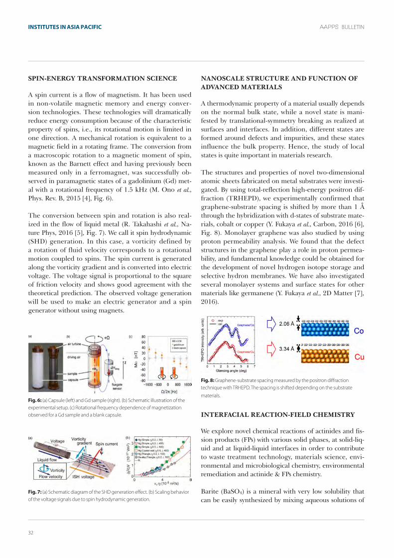
32
BULLETINinstitUtEs in asia PaCifiC
SPIN-ENERGY TRANSFORMATION SCIENCE
A spin current is a flow of magnetism. It has been used in non-volatile magnetic memory and energy conver-sion technologies. These technologies will dramatically reduce energy consumption because of the characteristic property of spins, i.e., its rotational motion is limited in one direction. A mechanical rotation is equivalent to a magnetic field in a rotating frame. The conversion from a macroscopic rotation to a magnetic moment of spin, known as the Barnett effect and having previously been measured only in a ferromagnet, was successfully ob-served in paramagnetic states of a gadolinium (Gd) met-al with a rotational frequency of 1.5 kHz (M. Ono et al., Phys. Rev. B, 2015 [4], Fig. 6).
The conversion between spin and rotation is also real-ized in the flow of liquid metal (R. Takahashi et al., Na-ture Phys, 2016 [5], Fig. 7). We call it spin hydrodynamic (SHD) generation. In this case, a vorticity defined by a rotation of fluid velocity corresponds to a rotational motion coupled to spins. The spin current is generated along the vorticity gradient and is converted into electric voltage. The voltage signal is proportional to the square of friction velocity and shows good agreement with the theoretical prediction. The observed voltage generation will be used to make an electric generator and a spin generator without using magnets.
fig. 6: (a) Capsule (left) and Gd sample (right). (b) Schematic illustration of the experimental setup. (c) Rotational frequency dependence of magnetization observed for a Gd sample and a blank capsule.
fig. 7: (a) Schematic diagram of the SHD generation effect. (b) Scaling behavior of the voltage signals due to spin hydrodynamic generation.
NANOSCALE STRUCTURE AND FUNCTION OF ADvANCED MATERIALS
A thermodynamic property of a material usually depends on the normal bulk state, while a novel state is mani-fested by translational-symmetry breaking as realized at surfaces and interfaces. In addition, different states are formed around defects and impurities, and these states influence the bulk property. Hence, the study of local states is quite important in materials research.
The structures and properties of novel two-dimensional atomic sheets fabricated on metal substrates were investi-gated. By using total-reflection high-energy positron dif-fraction (TRHEPD), we experimentally confirmed that graphene-substrate spacing is shifted by more than 1 Å through the hybridization with d-states of substrate mate-rials, cobalt or copper (Y. Fukaya et al., Carbon, 2016 [6], Fig. 8). Monolayer graphene was also studied by using proton permeability analysis. We found that the defect structures in the graphene play a role in proton permea-bility, and fundamental knowledge could be obtained for the development of novel hydrogen isotope storage and selective hydron membranes. We have also investigated several monolayer systems and surface states for other materials like germanene (Y. Fukaya et al., 2D Matter [7], 2016).
fig. 8: Graphene-substrate spacing measured by the positron diffraction technique with TRHEPD. The spacing is shifted depending on the substrate
materials.
INTERFACIAL REACTION-FIELD CHEMISTRY
We explore novel chemical reactions of actinides and fis-sion products (FPs) with various solid phases, at solid-liq-uid and at liquid-liquid interfaces in order to contribute to waste treatment technology, materials science, envi-ronmental and microbiological chemistry, environmental remediation and actinide & FPs chemistry.
Barite (BaSO4) is a mineral with very low solubility that can be easily synthesized by mixing aqueous solutions of

33
JUNE 2019 VOL. 29 NO. 3 institUtEs in asia PaCifiC
soluble salts such as barium chloride and sodium sulfate. Since barite can incorporate a variety of cations in its structure by coprecipitation, removal of divalent cations from aqueous solutions by coprecipitation with barite has been applied at an industrial scale. We succeeded in co-precipitating larger amounts of anions of Se(IV), Se(VI), and I(V) with barite by adjusting various parameters of coprecipitation (K. Tokunaga et al., Environ. Sci. Technol, 2017 [8], Fig. 9). The optimum coprecipitation condi-tions for those anions were different from each other but their distribution coefficients reached a level greater than 3×10³ mL/g. There were no methods to selectively incor-
porate those anions in inorganic solids with low solubil-ity. We are planning to immobilize barite coprecipitated with those anions in a solidified body and will investigate the barrier performance of a solidified body.
In addition, we have embraced the challenge of develop-ing novel waste treatment technologies for difficult-to-treat fission products, iodine and heptavalent techne-tium, to contribute to the acceleration of the Fukushima Daiichi nuclear power plant (FDNPP) decommissioning program.
fig. 9: Change of distribution coefficient Kd. (left) Se(IV) incorporation increased with crystal lattice distortion made by replacement of Ba2+ with Ca2+. (right) Se(IV) and Se(VI) incorporation increased with decreasing initial SO4
2- concentration.
fig. 10: Level schemes of the mirror hypernuclei, Λ4H and Λ4He. Λ binding energies (BΛ) of Λ4H(0+) and Λ4He(0+) are taken from past emulsion experiments. BΛ(Λ4He(1+)) and BΛ(Λ4H(1+)) are obtained using the present data and past γ-ray data.
fig. 11: A photograph of the ‘MINO’ event and its schematic drawing. The overlaid photograph is made by patching focused regions. Tracks #4, #5, #6, #8, and #9 are not fully shown in this photograph because these tracks are too long to be presented.

34
BULLETINinstitUtEs in asia PaCifiC
hiroyuki Koura is a principal researcher of the Advanced Science Research Center, Japan Atomic Energy Agency. After receiving a D. Sci from Waseda University, he worked for RIKEN as a collaborative scientist from 2001-2004. In 2004, he moved to the Advanced Science Research Center, Japan Atomic Energy Research Institute (JAERI) as a research scientist. He was a visiting scientist at Oak Ridge National Laboratory in 2005. He has been an adjunct researcher at Waseda University since 2012, a visiting scientist at RIKEN since 2013, a visiting professor of Ibaraki University since 2016, and a part-time lecturer of Tsuda University since 2017. His research interest is in nuclear physics, including superheavy elements and nucleosynthesis in stars.
Makoto oka is the director general of the Advanced Science Research Center, Japan Atomic Energy Agency (JAEA). After receiving a D. Sci from the University of Tokyo, he worked as a post-doctoral researcher at the Institute for Nuclear Study at the Univ. of Tokyo; Kobe Univ.; and Massachusetts Institute of Technology, and as an assistant professor at the Univ. of Pennsylvania. He then moved to the Tokyo Institute of Technology (Tokyo Tech) as an associate professor in 1991. He was a professor of physics at Tokyo Tech from 1996 to 2018 and moved to JAEA in April, 2018 as the director general of ASRC. He was a member of the Japan Science Council since 2006 (council member from 2011-2017) and has been a guest researcher of RIKEN since 2009. His research interests are in the fields of hadron physics, quantum chromodynamics, hadron spectroscopy and hadronic interactions.
HADRON NUCLEAR PHYSICS
We explore hadronic systems with strange and charm quarks mainly at J-PARC, and hot and dense quark/had-ronic matter at J-PARC.
In the study of Λ hypernuclei, we found an indication of large charge symmetry breaking in a ΛN interaction by measuring the difference between the first excited state and the ground-state for Λ
4He and Λ4H (T.O. Yamamoto
et al., Phys. Rev. Lett., 2017 [9], Fig. 10).
Furthermore, we found a beryllium double-Λ hyper-nucleus at J-PARC. This is the second of only two such events with a double-Λ hypernucleus and is a new species different from the previous event, a helium double-Λ hy-
pernucleus, known as the ‘NAGARA’ event in 2001. We named this new event the ‘MINO’ event (H. Ekawa et al., PTEP, 2019 [10], Fig. 11).
References
[1] T.K. Sato, et al., nature 520, 209 (2015).[2] r. Léguillon et al., Phys. Lett. b 761, 125 (2015).[3] Y. Tokunaga et al., Phys. rev. Lett. 114, 216401, (2015).[4] M. ono et al., Phys. rev. b 92, 174424 (2015).[5] r. Takahashi et al., nature Phys. 12, 52 (2016).[6] Y. fukaya et al., carbon 103, 1 (2016).[7] Y. fukaya et al., 2d Matter 3, 035019 (2016).[8] K. Tokunaga et al., environ. Sci. Technol. 51, 9194 (2017).[9] T.o. Yamamoto et al., Phys. rev. Lett. 115, 222501 (2017).[10] h. ekawa et al., Prog. Theor. exp. Phys. 2019, 021d02 (2019).

35
JUNE 2019 VOL. 29 NO. 3 institUtEs in asia PaCifiC
THE UNIvERSITY OF TOKYO (UTOKYO)
The University of Tokyo (UTokyo) was founded in 1877 and is the oldest national university in Japan. UTokyo has three main campuses, namely, Komaba campus with interdisciplinary links between established academic fields, Hongo campus with traditional academic activi-ties, and Kashiwa campus, which has the motto, “Adven-tures in Knowledge”. The Institute for Solid State Phys-ics (ISSP) moved to the then newly established Kashiwa
campus in 2000 and has explored a wide variety of phe-nomena exhibited by various materials from the view-point of the fundamental sciences, using the state-of-art experimental facilities and techniques. Materials under study include those that are critical for today’s high-tech society and those that will be integral for our society’s fu-ture development [1].
The Institute for Solid State Physics at The University of Tokyo
hATSUMI MorI dIrecTor, The InSTITUTe for SoILId STATe PhYSIcS, The UnIVerSITY of ToKYo
fig. 1: Yasuda Auditorium and the three main campuses (Kashiwa, Hongo, and Komaba) at The University of Tokyo.

36
BULLETINinstitUtEs in asia PaCifiC
THE INSTITUTE FOR SOLID STATE PHYSICS (ISSP)
ISSP, which became 62 years old in 2019, was established in 1957 as a joint-use research institute attached to UTo-kyo. During that time, with the support of the science community, we have aimed to lead in the frontiers of condensed matter and materials science and to contrib-ute to science and technology from the view of basic re-search. We have promoted activities focused on the areas of cutting-edge research, education for the next genera-tion, and joint-use/joint-research.
HISTORY ISSP was established as a National Joint-Use Research Institute attached to UTokyo in 1957.
1st generation (1957 – 1979); ISSP at UTokyo was established on April 1, 1957, as a joint-use/joint-research laboratory based upon the rec-ommendation of the Science Council of Japan and a concurrence between the Ministry of Education, Science and Culture and the Science and Technology Agency in order to lead fundamental research in condensed mat-ter physics. Within approximately the first 20 years, ISSP had achieved its original mission to serve as the central laboratory for materials science in Japan, equipped with the state-of-art facilities that were open for all domestic research with the objective of bringing research in Japan up to par with international levels.
2nd generation (1980 – 1995); The next goal was to develop advanced experimental techniques that were difficult to achieve in most univer-sity laboratories. The “second generation” reorganiza-tion of ISSP took place in 1980. The Division of Physics in Extreme Conditions included groups in the areas of ultra-high magnetic fields, laser physics, surface science, ultra-low temperatures and very high pressure. The Divi-sion of Physics in Extreme Conditions sought to create extreme conditions and to explore new phenomena. The Neutron Scattering Laboratory was constructed in Tokai in collaboration with the Japan Atomic Energy Agency. Its capabilities were significantly improved from 1990 – 1992, due to renovation of the research reactor. The Syn-chrotron Radiation Laboratory operated the SOR-RING in the Tanashi Campus of UTokyo and maintained beam lines in the Photon Factory at the High Energy Accelera-tor Research Organization (KEK) in Tsukuba. The Con-densed Matter Division and the Theory Division main-
tained small groups motivated by individual interests and ideas. From the fomer group, the Materials Develop-ment Division was formed in 1989, with the objective of exploring new materials and their novel properties.
3rd generation (1996 – present); In March 2000, ISSP relocated to a new campus of UTo-kyo in Kashiwa, after 43 years of activities at the Rop-pongi campus in downtown Tokyo. ISSP seeks to create new areas of science, in collaboration with other institu-tions in Kashiwa. In addition, a visiting staff division as well as two foreign visiting professor positions have been created. In 2003, the Neutron Scattering Laboratory was reorganized to become the Neutron Science Labora-tory. UTokyo was transformed into a “national university corporation” in 2004 and thus ISSP adopted a new role as a joint research laboratory in the university corpora-tion. In the same year, the Division of Frontier Areas Research changed its name to the Division of Nanoscale Science. In 2006, ISSP established the International MegaGauss Science Laboratory and started serving as an international center of physics in high magnetic fields. In 2011, the Center of Computational Materials Science was established at ISSP, with the objective of promot-ing materials science with advanced supercomputers. Regarding the Synchrotron Radiation Laboratory, after the closing of SOR-RING in 1997, the Harima branch of the Synchrotron Radiation Laboratory was established at SPring-8 in 2009. Furthermore, in 2012, the Division of Advanced Spectroscopy and the Synchrotron Radiation Laboratory (LASOR) were reorganized into the newly established Laser and Synchrotron Research Center. In 2016, the Divisions of New Materials Science and Physics in Extreme Conditions were reorganized into the Divi-sion of Condensed Matter Science, and the Functional Materials Group and the Quantum Materials Group were launched in order to widen the scope of condensed mat-ter sciences at ISSP, marking a new step forward in these interdisciplinary research fields. The Division of Data-Integrated Materials Science was established in 2019 as the first Social Cooperation Program at ISSP, working in collaboration with industrial groups. (Fig. 2)
FUNDAMENTALSThe organization of ISSP is depicted in Fig. 2. ISSP con-sists of four research divisions (Divisions of Condensed Matter Science, Condensed Matter Theory, Nanoscale Science, and Social Cooperation Programs), two inter-disciplinary groups (Quantum Materials and Functional Materials Groups), five research facilities (Materials De-

37
JUNE 2019 VOL. 29 NO. 3 institUtEs in asia PaCifiC
sign and Characterization Laboratory, Neutron Science Laboratory, International MegaGauss Science Labora-tory, Center of Computational Materials Science, and Laser and Synchrotron Research Center), supporting fa-cilities, and an administrative office. Since ISSP is a joint research/joint use institute, the management of ISSP reflects the perspectives of the research community; 1/4 of the members of ISSP’s advisory committee are recom-mended by the Science Council of Japan. Approximately half of ISSP’s selection committee and half of the advi-sory committee for joint research are also recommended by members of the physics and chemistry communities. There were 86 faculty members at ISSP in 2018: 27 professors, 16 associate professors, and 43 research as-sociates. In addition, 70 postdoctoral researchers, 30 technicians, and 12 administration staff members were affiliated with ISSP. Furthermore, in 2018, ISSP had 138 graduate students.
RESEARCHThe studies in condensed matter physics and materials science have three axes: (1) a conceptual axis (design), (2) a materials axis (synthesis), and (3) an investigation method axis (characterization) as shown in Fig. 3. These
three axes interact in what we call a DSC cycle, pro-moting innovative research. This institute is organized around 40 laboratories with the small-scale, and the medium-to-large-scale equipment and facilities. All labs work together to maintain the DSC cycle.
As for some of the most prominent findings from the DSC cycle at ISSP, the first Weyl antiferromagnet (Mn3Sn)
fig. 2: Organization of the Institute for Solid State Physics.
fig. 3: Design – Synthesis – Characterization (DSC) cycle in Research at ISSP.

38
BULLETINinstitUtEs in asia PaCifiC
was discovered, and the magnetic Weyl fermions were proved by laser angle-resolved photoemission spectros-copy (ARPES) measurements and density functional the-ory (DFT) calculations, as shown in Fig. 4. [2] The Weyl antiferromagnets reveal an anomalous Hall effect and a Nernst effect, leading to more efficient coverage of the heat source.
Another significant achievement was reported from one of our large-scale facility, the International MegaGauss Science Laboratory. The world record for an indoor
magnetic field of 1,200 T was generated by electromag-netic flux compression at ISSP in 2018 (Fig. 5) [3]. The achievement has opened up some interesting possibili-ties, such as the development of new kinds of electronic devices and the elucidation of biological chirality related to the origins of life.
JOINT USE and JOINT RESEARCHISSP has been established for joint research with con-densed matter scientists in Japan. After UTokyo trans-formed from a national university to a “national uni-versity corporation”, ISSP was authorized as a joint-use/research center in 2009, and its joint-use programs with the newly authorized status started in 2010. ISSP has a variety of systems supporting such joint-research activi-ties; continuously, numerous outside researchers visit ISSP and utilize our facilities. The ISSP joint-research program is operated by two committees consisting of ISSP faculty members, and of board members external to our laboratory operations recommended by the physics and chemistry communities.
The facilities of ISSP are open to researchers in Japan, who are encouraged to submit joint research proposals. The submission of research proposals is received twice a year, and the proposals are selected by the Advisory Committee for Joint Research. In addition, ISSP pro-vides opportunities for young scientists, including gradu-ate students from across the country, to do research for extended periods of time. For those visitors, ISSP assists with their travel and research expenses.
Figure 6 shows that around 1,400 domestic and foreign researchers visited ISSP and approximately 8,000 (re-searchers • days) visitors took part in joint use and joint research in 2017. Moreover, ISSP holds domestic and in-
fig. 4: The first Weyl antiferromagnet (Mn3Sn) was discovered and the magnetic Weyl fermions were proved by angle-resolved photoemission spectroscopy (ARPES) measurements and density functional theory (DFT) calculations. [2]
fig. 5: The world record for an indoor magnetic field of 1,200T was generated by electromagnetic flux compression at ISSP in 2018. [3]

39
JUNE 2019 VOL. 29 NO. 3 institUtEs in asia PaCifiC
ternational workshops and symposia on specific subjects of condensed matter science. A typical workshop is two to three days long and approximately 1,400 people par-ticipated in 2017. Proposals for workshops are submitted by researchers across Japan and are selected by the Advi-sory Committee for Joint Research.
DEvELOPMENT OF HUMAN RESOURCESISSP contributes to graduate education in condensed matter science through its unique facilities. Currently, the faculty members participate in the following de-partments of the graduate school of UTokyo: physics, chemistry (Graduate School of Science), applied physics (Graduate School of Engineering), advanced materi-als, and complexity science and engineering (Graduate School of Frontier Sciences).
In 2018, there were 89 graduate students in the master’s program and 49 graduate students in the doctor’s pro-gram. In recent years, female students have accounted for fewer than 10 percent of the student body ; however, through outreach programs, we hope to increase the number of women studying at ISSP.
Every year, in May, ISSP hosts its graduate program in-formation session for future students to explain the sys-tem of graduate school programs, to introduce research groups/laboratories at ISSP, to provide guided tours to the laboratories and related facilities for the participants, and to provide other necessary information.
ISSP’s various initiatives to foster and develop young re-searchers include lectures and training sessions organized by the Center of Computational Materials Science (CCMS).
The center hosts and provides lecturers for lectures and training sessions in the Kashiwa campus and the Kobe branch. Its monthly training program, Kashiwa/Kobe Hands-On, provides an opportunity for young researchers to get accustomed to various application programs.
ISSP also contributes to the development of young re-searchers in related fields. For instance, ISSP members participate in educational programs for domestic and international researchers held at large synchrotron and neutron facilities. In addition to sending lecturers, ISSP is engaged in organizing and operating such programs as a co-host organization.
INTERNATIONAL ACTIvITIESISSP plays an important role as an international center of materials science. There are various international col-laboration programs at ISSP such as (1) two positions per year for foreign visiting professorships for 3-12 months, (2) visiting researcher/scientist positions for 1-3 months, (3) international collaboration research of a duration within two weeks, and (4) international research op-portunities for ISSP students lasting for more than four weeks. The unique facilities of ISSP have been used in many international and collaborative activities. Many foreign researchers have spent their early careers at ISSP, supported by various fellowship programs sponsored by ISSP, the Japan Society for the Promotion of Science (JSPS), and other agencies.
Moreover, in order to promote international activities, a global collaboration system was initiated at ISSP in 2018. The ISSP task force team, composed of members in the fields of high magnetic fields, pressure, neutron science,
fig. 6: Statistics for joint use and joint research in regard to ISSP workshops and symposia held at ISSP. Around 1,400 domestic and foreign researchers visited ISSP in 2017. Several ISSP events, consisting of workshops and symposia, have been held yearly; there were approximately 1,400 participants in 2017.
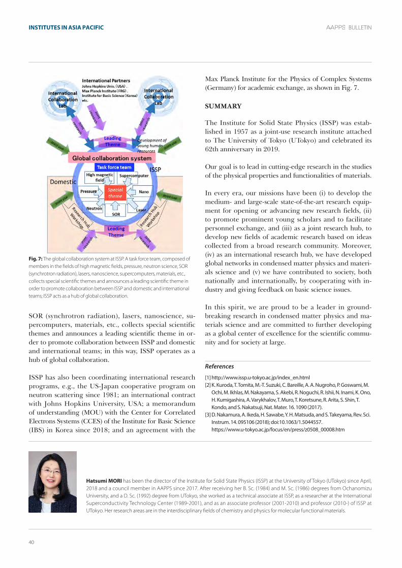
40
BULLETINinstitUtEs in asia PaCifiC
hatsumi Mori has been the director of the Institute for Solid State Physics (ISSP) at the University of Tokyo (UTokyo) since April, 2018 and a council member in AAPPS since 2017. After receiving her B. Sc. (1984) and M. Sc. (1986) degrees from Ochanomizu University, and a D. Sc. (1992) degree from UTokyo, she worked as a technical associate at ISSP, as a researcher at the International Superconductivity Technology Center (1989-2001), and as an associate professor (2001-2010) and professor (2010-) of ISSP at UTokyo. Her research areas are in the interdisciplinary fields of chemistry and physics for molecular functional materials.
SOR (synchrotron radiation), lasers, nanoscience, su-percomputers, materials, etc., collects special scientific themes and announces a leading scientific theme in or-der to promote collaboration between ISSP and domestic and international teams; in this way, ISSP operates as a hub of global collaboration.
ISSP has also been coordinating international research programs, e.g., the US-Japan cooperative program on neutron scattering since 1981; an international contract with Johns Hopkins University, USA; a memorandum of understanding (MOU) with the Center for Correlated Electrons Systems (CCES) of the Institute for Basic Science (IBS) in Korea since 2018; and an agreement with the
Max Planck Institute for the Physics of Complex Systems (Germany) for academic exchange, as shown in Fig. 7.
SUMMARY
The Institute for Solid State Physics (ISSP) was estab-lished in 1957 as a joint-use research institute attached to The University of Tokyo (UTokyo) and celebrated its 62th anniversary in 2019.
Our goal is to lead in cutting-edge research in the studies of the physical properties and functionalities of materials.
In every era, our missions have been (i) to develop the medium- and large-scale state-of-the-art research equip-ment for opening or advancing new research fields, (ii) to promote prominent young scholars and to facilitate personnel exchange, and (iii) as a joint research hub, to develop new fields of academic research based on ideas collected from a broad research community. Moreover, (iv) as an international research hub, we have developed global networks in condensed matter physics and materi-als science and (v) we have contributed to society, both nationally and internationally, by cooperating with in-dustry and giving feedback on basic science issues.
In this spirit, we are proud to be a leader in ground-breaking research in condensed matter physics and ma-terials science and are committed to further developing as a global center of excellence for the scientific commu-nity and for society at large.
References
[1] http://www.issp.u-tokyo.ac.jp/index_en.html [2] K. Kuroda, T. Tomita, M.-T. Suzuki, c. bareille, A. A. nugroho, P. goswami, M.
ochi, M. Ikhlas, M. nakayama, S. Akebi, r. noguchi, r. Ishii, n. Inami, K. ono, h. Kumigashira, A. Varykhalov, T. Muro, T. Koretsune, r. Arita, S. Shin, T. Kondo, and S. nakatsuji, nat. Mater. 16. 1090 (2017).
[3] d. nakamura, A. Ikeda, h. Sawabe, Y. h. Matsuda, and S. Takeyama, rev. Sci. Instrum. 14. 095106 (2018); doi:10.1063/1.5044557. https://www.u-tokyo.ac.jp/focus/en/press/z0508_00008.htm
fig. 7: The global collaboration system at ISSP. A task force team, composed of members in the fields of high magnetic fields, pressure, neutron science, SOR (synchrotron radiation), lasers, nanoscience, supercomputers, materials, etc., collects special scientific themes and announces a leading scientific theme in order to promote collaboration between ISSP and domestic and international teams; ISSP acts as a hub of global collaboration.
41
JUNE 2019 VOL. 29 NO. 3 PhYsiCs foCUs
ABSTRACT
In magnetic materials with geometrically frustrated inter-actions in triangular, kagome, or pyrochlore lattice sys-tems, various kinds of nontrivial orderings are observed; e.g., non-collinear and incommensurate spin structures, as well as successive transitions through partially disor-dered states. Most of these orderings are difficult to pre-dict because in general a large number of spin structures are degenerate. Recently, we have found a novel ordering phenomenon realized in a distorted kagome lattice of S = 7/2 4f-spins of Gd ions in Gd3Ru4Al12, which effective-ly can be considered to be a triangular lattice of S = 21/2 spin trimers. First, it is very rare that quantum mechanical multimerization is realized in localized and metallic f-electron systems. Second, it is significant that a spontane-ous chiral symmetry breaking was found in the process of sinusoidal to helical successive phase transitions.
INTRODUCTION
Cooperative phenomenon among interacting electrons gives rise to a diversity of spontaneous ordering struc-tures. Even in simple structures of ferromagnetic and antiferromagnetic orderings, where electron spins align in parallel and antiparallel ways, respectively, the details of the magnetic exchange interactions are widely var-ied. If the magnetic ions are located on a triangular or kagome lattice, and if the exchange interaction is antifer-romagnetic, one cannot find a simple structure to satisfy the interactions consistently. In such cases, the system usually ends up with a so-called 120° structure as a result of compromises being made. In the crystal structure of Gd3Ru4Al12 shown in Fig. 1, with a distorted kagome, or breathing kagome lattice, one may simply speculate that a 120° spin structure should be realized.
SPIN TRIMER FORMATION
In Gd3Ru4Al12, Nakamura et al. recently pointed out that the Gd3+ spins of S = 7/2 on the nearest neighbor tri-angle form a “spin trimer” state with S = 21/2 [1]. They showed that the anomalous temperature dependence of the magnetic susceptibility and specific heat can be well explained by a spin trimer model H = J(S1•S2 +S1•S2 +S1•S2) with a ferromagnetic exchange constant of J=13.5 K. Although such quantum spin states are fre-quently observed in insulating d-electron systems with small spin moments, they are rarely observed in mostly metallic f-electron systems with relatively large angular moments. Only one exception is a spin dimer formation in YbAl3C3 [2]. The spin trimer formation in Gd3Ru4Al12 may be the first known case in f-electron systems.
HELICAL ORDERING OF SPIN TRIMERS
Another interesting property found in Gd3Ru4Al12 is the successive magnetic phase transitions at 18.5 K and 17.5 K. Since the binding energy of the spin trimer is higher than 100 K, these phase transitions at low tem-peratures are considered to be the orderings among well developed spin trimers. To investigate the ordered spin structure, we have utilized a resonant X-ray diffraction method using synchrotron radiation at the Photon Fac-tory, High Energy Accelerator Research Organization, in Tsukuba, Japan. Element and orbital selectivity by using X-ray energies near the absorption edge of the target el-ement, effective usage of a polarized incident beam and polarization analysis, high Q-resolution, applicability of tiny samples, and applicability to the neutron absorbing elements like Gd, are the advantages of resonant X-ray diffraction over neutron diffraction, which is a typical method used to investigate magnetic structures.
Helical Ordering of Spin TrimersFound in a Distorted Kagome Lattice
TAKeShI MATSUMUrA grAdUATe SchooL of AdVAnced ScIenceS of MATTer, hIroShIMA UnIVerSITY

42
BULLETINPhYsiCs foCUs
Through careful measurements and data analysis, es-pecially from the results of the polarization analysis, we concluded that the transition at 18.5 K is an ordering of spin trimers from a paramagnetic to sinusoidal structure, and that the transition at 17.5 K is a transition from a si-nusoidal to helical structure; these transitions are shown in Fig. 1.
fig.1: (a) Helical trimer spin structure below 17.5 K, propagating along the a*-axis. The total spins of each trimer is represented by the bigger arrows at the center of colored triangles. (b) Sinusoidal trimer spin structure between 17.5 K and 18.5 K.
An important problem of this sinusoidal structure is that there remain magnetic sites with small or even vanishing ordered moments. This means that unreleased magnetic entropy or degeneracy remains, which must be lifted at lower temperatures. The sinusoidal structure just below the Néel order reflects the weak anisotropy in the c-plane and the preferable propagation vector of (0.27, 0, 0) for the magnetic exchange interaction via the conduction electrons. However, it is not preferable to maintain this collinear structure down to lower temperatures due to the thermodynamic reason of magnetic entropy.
The spin system of Gd3Ru4Al12 chooses to become helical
below 17.5 K by inducing the c-axis spin component, i.e., by transforming the structure into a non-collinear form. In other words, the chiral degeneracy in the sinusoidal structure is lifted spontaneously by the transition to the helical structure, which allows all the Gd spins to fully develop.
Chirality plays an important role in a wide range of fields in nature, from biology, chemistry, and particle physics to materials science. Recently, in magnetic materials with a chiral crystal structure, the emergence of nontrivial chiral objects such as skyrmions and chiral soliton lat-tices have been attracting wide interest both for applica-tions and basic science. Although the crystal structure of Gd3Ru4Al12 is not chiral, the present discovery of the spontaneous breaking of chiral symmetry is expected to stimulate further research and deeper understanding of chiral magnets [4].
Acknowledgements: This work was supported by JSPS KAKENHI Grant number 18K187370A. The synchro-tron experiments were performed under the approval of the Photon Factory Program Advisory Committee (No. 2018G039).
References
[1] S. nakamura, n. Kabeya, M. Kobayashi, K. Araki, K. Katoh, and A. ochiai, Phys. rev. b 98, 054410 (2018).
[2] A. ochiai, T. Inukai, T. Matsumura, A. oyamada, and K. Katoh, J. Phys. Soc. Jpn. 76, 123703 (2007).
[3] T. Matsumura, Y. ozono, S. nakamura, n. Kabeya, and A. ochiai, J. Phys. Soc. Jpn. 88, 023704 (2019).
[4] h. Amitsuka, JPSJ news and comments 16, 06 (2018).
Reference 3 was published on 28 January 2019 of the on-line version of the Journal of the Physical Society of Japan as an Editor’s Choice article.
takeshi Matsumura is an associate professor at the Graduate School of Advanced Sciences of Matter, Hiroshima University. After receiving his D.Sci from Tohoku University, he worked as a post-doc at University College London and as an assistant professor at Tohoku University, before joining Hiroshima University in 2007. His research field is magnetism in strongly correlated electron systems.

43
JUNE 2019 VOL. 29 NO. 3 soCiEtY nEWs
In recognition of important achievements toward prog-ress in physics, the Physical Society of Japan (JPS) an-nually selects outstanding papers from among original research articles published in the Journal of the Physical Society of Japan, Progress of Theoretical Physics, Progress of Theo-retical and Experimental Physics, and JPS Conference Proceed-ings. The selection committee has chosen five papers for the 2019 award based on 16 nominations (for 15 papers) made by the editors of the JPS journals and representa-tives of the 19 divisions of the JPS.
On the morning of March 16, 2019, the 2019 award cer-emony was held at Shiiki Hall, Kyushu University.
The titles of the five selected papers, together with their citations, follow below.
Locally Non-centrosymmetric Superconductivity in Multilayer SystemsJ. Phys. Soc. Jpn. 81, 034702 (2012)Authors: Daisuke Maruyama, Manfred Sigrist, and Youichi Yanase
The effects of crystallographic symmetries on supercon-ductivity have attracted considerable research attention recently. In particular, the consequences of the absence of inversion symmetry on superconductivity have been vigorously examined. In this study, the authors further developed this trend by theoretically studying supercon-ductivity in layered materials that have an inversion sym-metry but also possess some layers that do not coincide with mirror planes. In these types of systems, the lack of a mirror symmetry on these planes results in an effective modulated Rashba spin-orbit interaction, which produc-es various physical effects. The authors found that the
induced Rashba spin-orbit interaction considerably in-creases the upper critical field of superconductivity. This well explains experimental observations in artificially en-gineered heavy-fermion superlattices based on CeCoIn5 as well as in BiS2-based layered materials. Furthermore, the induced Rashba spin-orbit interaction as predicted in this study has recently been directly confirmed by an ARPES measurement in LaO0.55 F0.45BiS2.
This study opens the possibility of controlling properties of materials, such as their superconductivity, by locally de-stroying the inversion symmetry. Indeed, some of the pre-dictions suggested in this study have already been verified in a recent experiment. Given the recent developments in artificial engineering of lattice structures, we expect that the importance of this study will increase. For these rea-sons, we conclude that this paper deserves the Outstand-ing Paper Award of the Physical Society of Japan.
Commensurate Itinerant Antiferromagnetism in BaFe2As2: 75As-NMR Studies on a Self-Flux Grown Single CrystalJ. Phys. Soc. Jpn. 77, 114709 (2008)Authors: Kentaro Kitagawa, Naoyuki Katayama, Kenya Ohgushi, Makoto Yoshida, and Masashi Takigawa
This study reports on fundamental research on the mag-netism of the parent material of iron-based superconduc-tors discovered by the Hosono Group in 2008. Through precise measurements and the analysis of magnetic reso-nance, the authors clarified that the As nucleus works as an excellent probe of the electronic states of this system and found that the antiferromagnetic transition of this system is of first order. Researchers of magnetic reso-
The Physical Society of Japan Announces the Recipients of the 24th Outstanding Paper Award

44
BULLETINsoCiEtY nEWs
nance for other iron-based superconductors make wide use of the hyperfine interaction tensor that was deter-mined from the authors’ analysis based on the assump-tion of a magnetic structure revealed by neutron scatter-ing. In addition, the authors detected from the change of the electric field gradient the structural phase transition that occurs simultaneously with the antiferromagnetic phase transition. This represents pioneering research on the nematic phase transition in the present system, which now has become popular.
As 2008 was the year when the superconducting state was discovered in iron-based compounds, many researchers focused on elucidating this state. This work, however, moved one step away from superconductivity and fo-cused on the magnetism of the parent material and con-sequently this work has been instrumental in establishing a foundation for the study of iron-based superconduc-tors. Thus, we conclude that this paper deserves the Out-standing Paper Award of the Physical Society of Japan.
Line-Node Dirac Semimetal and Topological Insulating Phase in Noncentrosymmetric Pnictides CaAgX (X = P, As)J. Phys. Soc. Jpn. 85, 013708 (2016)Authors: Ai Yamakage, Youichi Yamakawa, Yukio Tanaka, and Yoshihiko Okamoto
This study theoretically predicted that a topological line node emerges as a result of the mirror-reflection symme-try in the band structure of noncentrosymmetric material CaAgX (X = P, As) in the absence of spin-orbit interac-tion. Combining analytical theory based on topology with first-principles electronic-state calculations, the au-thors produced a qualitatively clear and quantitatively re-liable prediction. Although this is not the first theoretical report on the topological line node protected by mirror-reflection symmetry, the fact that the authors specified the material group of CaAgX has been highly regarded as the authors discovered a new topological material group in addition to finding a means to verify experi-mentally the physical effects of line nodes. In 2018, the authors experimentally verified line nodes in a CaAgAs single crystal through angle-resolved photoemission spectroscopy.
Thus, in recognition of this study having identified a new topological material group that was later experimen-tally verified, this paper deserves the Outstanding Paper Award of the Physical Society of Japan.
Deep Learning the Quantum Phase Transitions in Random Two-Dimensional Electron SystemsJ. Phys. Soc. Jpn. 85, 123706 (2016)Authors: Tomoki Ohtsuki and Tomi Ohtsuki
Machine learning, particularly its variation known as deep learning, recently has shown tremendous progress. Its remarkable success in numerous practical applica-tions, such as image recognition, is notable. The mecha-nisms of machine learning may be related to statistical mechanics, which deal with many interacting elements. Although several attempts to understand machine learn-ing based on statistical mechanics have been made, this problem remains unresolved. This study applied deep learning to a quantitative analysis of quantum phase transitions, which is one of the most fundamental prob-lems in statistical mechanics. As a concrete problem, the authors studied the localized-delocalized transition of a single particle in random potentials. For two-dimension-al random potentials with symplectic symmetry, single-particle eigenstates are known to exhibit the Anderson transition, which is a quantum phase transition between a delocalized (metallic) phase and a localized (insulator or Anderson-localized) phase. Energy eigenfunctions in the delocalized phase spread over the entire system, just as plane-wave states do in a free space. In contrast, energy eigenfunctions in the localized phase are local-ized in a finite region. However, distinguishing these two cases from numerically obtained eigenfunctions in small systems is not easy. In this study, the authors regarded the probability distribution (absolute value squared of the eigenfunction) as an “image” to which machine-learning techniques for image recognition were applied. They successfully demonstrated that the two phases can be dis-tinguished from eigenfunctions in a relatively small sys-tem. Although some previous studies on the applications of machine learning to the detection of phases or phase transitions were conducted, the success of this study on the Anderson transition, as well as the topological phase transition between a Chern insulator and an Anderson-localized phase, established this study’s usefulness. Today, applications of machine learning to statistical mechanics are being vigorously studied at research centers around the world. As a pioneering study that provides a founda-tion for an active field of research, this paper deserves the Outstanding Paper Award of the Physical Society of Japan.

45
JUNE 2019 VOL. 29 NO. 3 soCiEtY nEWs
Mobility of Ions Trapped Below a Free Surface of Superfluid 3HeJ. Phys. Soc. Jpn. 82, 124607 (2013)Authors: Hiroki Ikegami, Suk Bum Chung, and Kimitoshi Kono
The supersymmetry theory predicts that Majorana fer-mions exist. Recently, the search for these hypothetical elementary particles as quasiparticles in topological matters has attracted considerable attention from the viewpoint of fundamental physics and in applications to topological quantum computation. The 3He-B phase is a time-reversal invariant topological superfluid with Cooper pairing in the Balian-Werthamer state that has a spin triplet p-wave symmetry. Majorana fermions are theoretically expected to emerge at surfaces of 3He-B. Recent experiments suggest the existence of these types of quasiparticles when measuring the surface Andreev bound state at an interface between 3He-B and a solid.
This study succeeded in developing a unique and so-phisticated technique to measure the mobility of nega-tive or positive ions trapped in a two-dimensional plane 20–60 nm beneath a free surface of 3He-B. With the aid of this technique, the authors found that ion mobilities, which are dominated by quasiparticle scattering, do not depend on the depth of the ions and they concluded,
after carefully considering various spurious effects, that this should be an intrinsic property of the system. Quite recently, this apparently strange result has been quanti-tatively and theoretically explained by considering the scattering cross section at the quasi-bound state around the negative ion that is actually an electron bubble. This means that the measured depth-independent mobility does indicate the existence of surface Majorana fermi-ons. The authors also measured the ion mobility of both the B phase and the chiral superfluid A phase in a much wider temperature range (250 μK ≤ T ≤ Tc = 930 μK) than in previous works. They found that the tempera-ture dependences near Tc are consistent with theoretical calculations that consider the p-wave coherence in scat-tering of Bogoliubov quasiparticles for both the B and A phases, particularly for negative ions.
In conclusion, through this newly developed technique that uses two-dimensional ion systems trapped just beneath a free superfluid surface, this study provides further experimental support for the emergence of Ma-jorana fermions protected by time reversal symmetry in topological superfluids and is, thus, a major contribu-tion to the field. Therefore, we conclude that this paper deserves the Outstanding Paper Award of the Physical Society of Japan.

46
BULLETINsoCiEtY nEWs
The purpose of DACG is to promote scientific activities in the areas of astrophysics, cosmology and gravitation in the Asia Pacific region. In particular, the CosPA meetings, a series of International Symposia on Cosmology and Particle Astrophysics, organized by the Asia-Pacific Cosmology and Particle Astrophysics (APCosPA) committee, are one of the major scientific activities we endorse. The first CosPA was held in Taiwan in 2003. The 17th symposium, CosPA2018, was hosted by the Center for Gravitation and Cosmology at Yangzhou University, held from 19 to 23, November 2018, and attended by over 180 participants from 10 countries and regions. There were three plenary sessions with18 plenary talks. One of the sessions was dedicated to the memory of Prof. Pauchy Hwang, one of the founders of CosPA, who suddenly passed away in May 2018. In addi-tion, parallel sessions were arranged which accommodated 45 talks. The participants discussed in depth the current situations as well as future research prospects in astrophysics, cosmology and gravitation. One of the highlights was a plenary talk by Prof. Jun Luo, the President of Sun Yat-sen University, who introduced the space-based gravitational wave detection project, “TianQin (Heav-enly Harp).” As in the previous year, taking advantage of the fact that many of the executive committee (EXCO)
Recent Activities of the Division of Astrophysics Cosmology and Gravitation (DACG)
MISAo SASAKI chAIr of dAcg
Prof. Jun Juo introducing TianQin at CosPA2018, Yangzhou.
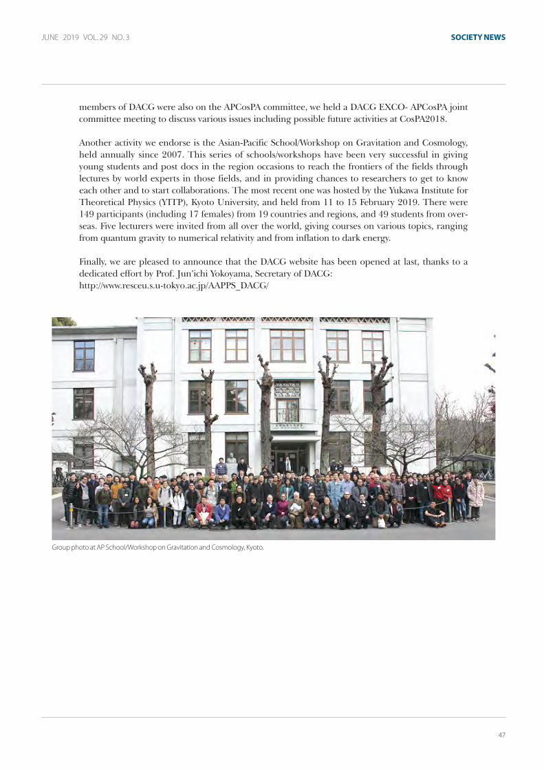
47
JUNE 2019 VOL. 29 NO. 3 soCiEtY nEWs
Group photo at AP School/Workshop on Gravitation and Cosmology, Kyoto.
members of DACG were also on the APCosPA committee, we held a DACG EXCO- APCosPA joint committee meeting to discuss various issues including possible future activities at CosPA2018.
Another activity we endorse is the Asian-Pacific School/Workshop on Gravitation and Cosmology, held annually since 2007. This series of schools/workshops have been very successful in giving young students and post docs in the region occasions to reach the frontiers of the fields through lectures by world experts in those fields, and in providing chances to researchers to get to know each other and to start collaborations. The most recent one was hosted by the Yukawa Institute for Theoretical Physics (YITP), Kyoto University, and held from 11 to 15 February 2019. There were 149 participants (including 17 females) from 19 countries and regions, and 49 students from over-seas. Five lecturers were invited from all over the world, giving courses on various topics, ranging from quantum gravity to numerical relativity and from inflation to dark energy. Finally, we are pleased to announce that the DACG website has been opened at last, thanks to a dedicated effort by Prof. Jun’ichi Yokoyama, Secretary of DACG:http://www.resceu.s.u-tokyo.ac.jp/AAPPS_DACG/

48
BULLETINaPCtP sECtion
doI: 10.22661/AAPPSbL.2019.29.3.48
We have studied a frustrated anisotropic four-leg spin-1/2 nanotube using a real space quantum renormalization group (QRG) approach in the thermodynamic limit. We show that in the limit of weakly interacting plaquettes, the model is mapped onto a 1D spin-1/2 XXZ chain in a longitudinal magnetic field under QRG transformation. Analysis of the effective Hamiltonian reveals that the spin nanotube displays both first and second order phase transitions accompanied by fractional magnetization plateaus. We also show that the anisotropy significantly changes the magnetization curve and the location of phase transition points. Moreover, using a numerical ex-act diagonalization method, the ground state phase dia-gram was studied. Our numerical results are in complete agreement with the known analytical results.
INTRODUCTION
Frustrated spin systems are known to have many in-triguing properties that are different from conventional magnetic systems [1, 2]. Frustration induces unconven-tional magnetic orders [1–3] or even a disorder [1, 2]. The study of frustrated systems has attracted much more attention with the discovery of J1 – J2 chain materials like CuGeO3 [4], and has been developed by synthesiz-ing of odd number (n) of the legs spin tube, such as [(CuCl2tachH)3 Cl]Cl2 [5] and CsCrF4 [6] with n = 3, and Na2V3O7 [7] with n = 9. Spin tubes with an odd number of legs and only nearest neighbor antiferromagnetic (AFM) intrachain coupling are geometrically frustrated. According to the Lieb-Schultz-Mattis theorem [8], the ground state of such systems is either gapped with a bro-
ken translational invariance, or gapless (non- degener-ate) [9].
Recently, four-leg spin-1/2 nanotube Cu2Cl4D8C4SO2, with next-nearest neighbor (NNN) AFM interaction, di-agonally coupling adjacent legs, has been established as a new frustrated spin tube [10–12] (Fig. 1).
fig. 1: A schematic plot of a frustrated four-leg spin tube. The interaction along the legs is characterized by J1 (red lines) and J0 shows the intra-plaquettes interaction (black lines). The diagonal interaction Jd has been shown by the green lines.
The Hamiltonian of the geometrically frustrated anisotro-pic four-leg spin tube (FAFST) model in the presence of a magnetic field on a periodic tube of N sites is given by
(1)
where we define
Magnetization Plateaus in a Geometrically Frustrated Anisotropic Four-Leg Nanotube
r. JAfArI,1, 2, * SAeed MAhdAVIfAr,3 And ALIreZA AKbArI4, 5, 6, 1 1 dePArTMenT of PhYSIcS, InSTITUTe for AdVAnced STUdIeS In bASIc ScIenceS (IASbS), ZAnJAn 45137-66731, IrAn
2 dePArTMenT of PhYSIcS, UnIVerSITY of goThenbUrg, Se 412 96 goThenbUrg, Sweden 3 dePArTMenT of PhYSIcS, UnIVerSITY of gUILAn, 41335-1914, rAShT, IrAn
4 ASIA PAcIfIc cenTer for TheoreTIcAL PhYSIcS (APcTP), PohAng, gYeongbUK, 790-784, KoreA 5 dePArTMenT of PhYSIcS, PoSTech, PohAng, gYeongbUK 790-784, KoreA
6 MAX PLAncK PoSTech cenTer for coMPLeX PhASe MATerIALS, PoSTech, PohAng 790-784, KoreA

49
JUNE 2019 VOL. 29 NO. 3 aPCtP sECtion
(2)
with n = (0, 1, d). Here J0 > 0, J1 > 0 and Jd > 0 are the plaquette, leg, and diagonal exchange couplings respec-tively, and the corresponding easy-axis anisotropies are defined by ∆0, ∆1 and ∆d. Furthermore, σ = (σx, σy, σz) denotes the Pauli matrices, and h represents a magnetic field to point along the z-direction. Without loss of the generality, we now rescale all the energy parameters in the unit of J0 by considering J0 = 1.
Four leg spin tubes with only nearest neighbor AFM exchange are not frustrated and have been studied [9, 13–17]. Although the magnetic properties of the FAFST model have been investigated in a few papers [9, 18], an understanding of the quantum phases of the FAFST model on a larger scale is still missing [9]. In addition, the phase diagram and universality class of the model in the presence of anisotropy is unknown. Thus, we are mo-tivated to investigate the FAFST model in the presence of a magnetic field, in the strong plaquette coupling limits, using the real space renormalization group (RSQRG) ap-proach. We show that, in the strong plaquette coupling limit, under RSQRG transformation, the FAFST model maps onto the one-dimensional (1D) spin-1/2 XXZ mod-el in the presence of an effective magnetic field. We also show that when the leg and frustrating couplings are the same (maximum frustration line), only first order quan-tum phase transitions are observed at zero temperature. The magnetization per particle process exhibits fractional plateaus at zero, one-quarter, one-half and three-quarter of the saturation magnetization. Away from the maximum frustrating line, the model exhibits both first and second order quantum phase transitions. In addition, we applied the numerical Lanczos method for the finite size spin-1/2 nanotubes and the obtained results fully agreed with the QRG and support the mentioned behaviors.
REAL SPACE QUANTUM RENORMALIZATION GROUP
Real space quantum renormalization group (RSQRG) method can be chosen to study lattice systems when deal-ing with zero temperature properties of many-body sys-tems with a large number of strongly correlated degrees of freedom [19–22]. Application of the RSQRG on lattice systems implies the construction of a new smaller system corresponding to the original one with new (renormalized) interactions between the degrees of freedom [23–25].
In this paper we have implemented Kadanoff’s block method to study FAFST. In Kadanoff’s method, the lat-tice is divided into disconnected blocks of nB sites each where the Hamiltonian is exactly diagonalized. This par-tition of the lattice into blocks induces a decomposition of the Hamiltonian ℋ into an intrablock Hamiltonian ℋB and an interblock Hamiltonian ℋBB where the block Hamiltonian ℋB is the sum of the commuting terms
each acting on the Ith block of the chain. Each block is treated independently to build the projec-tion operator P0 onto the lower energy subspace. The projection of the Hamiltonian is mapped to an effective Hamiltonian ℋeff that acts on the renormalized subspace where the interaction between blocks defines the effec-tive interaction of the renormalized chain, where each block is considered as a new single site. The perturbative implementation of this method has been discussed com-prehensively [3, 20, 21], and the effective Hamiltonian up to first order corrections is given by
(3)
with
fig. 2: A schematic plot of the decomposition of a four-leg spin tube into plaquette blocks where each plaquette is replaced by an effective single site under the renormalization process.
RENORMALIZATION OF THE MODEL WITH STRONG PLAQUETTE COUPLING (WEAKLY INTERACTING PLAQUETTES)
To apply the QRG scheme to the model in the strong plaquette coupling limit, we consider the Hamiltonian of Eq. (1), and we split the spin tube into blocks where

50
BULLETINaPCtP sECtion
each contains an independent plaquette (see Fig. 2). The Hilbert space of each plaquette has sixteen states, which consists of two spin-0 singlets, nine spin-1 triplets and five spin-2 quintuplets [18]. The plaquette Hamiltonian and the four lowest eigenvalues of the plaquette Hamil-tonian labeled by e0, e1, e2, e3, and their corresponding eigenstates are given in the appendix. Since energy level crossing occurs between the four lowest eigenstates of the block Hamiltonian, the projection operator, P0, can be different depending on the coupling constants. Thus, we specify the regions with the corresponding two lowest eigenvalues to construct their projection operators. We will discuss the phase diagram in terms of the following five different regions, which are classified by the two low-est eigenvalues of the plaquette Hamiltonian.
Region I: e0 as a ground state and e2 as a first excited stateIn this region we have h < ∆0 – 1, and to the first order corrections the effective Hamiltonian leads to the 1D ex-actly solvable transverse field Ising model, i.e.,
(4)
Here
(5)
with
The 1D Ising model in a transverse field is exactly solvable by the Jordan-Wigner transformation [8] and the RSQRG [20]. For simplicity, we consider isotro-pic interaction on the plaquette ∆0 = 1. Then, the renormalized coupling and transverse field reduces to J′ = 2(∆d – ∆1)/3, and h′ = 1/J′ . The phase transi-tion between the paramagnetic and antiferromag-netic/ferromagnetic phases takes place at h′ = 1, under which the system is ferromagnet (∆1 < ∆d) or antiferromagnet (∆1 > ∆d) while the system en-ters the paramagnetic phase above the critical point h′ > 1. It is remarkable that, by assuming equal anisot-ropy ratios for the leg and diagonal interactions ∆1 = ∆d, the system is always in the paramagnetic phase, where spins align along the direction of the external magnetic field.
Region II: e0 as a ground state and e1 as a first excited stateIn the region II, we have
where e0 and e1 are the ground state and the excited state of the plaquette Hamiltonian, respectively. This leads the effective Hamiltonian to the well-known 1D XXZ model in the presence of an external magnetic field, which can be solved exactly by the Bethe Ansatz method [26, 27]
(6)
where the couplings of renormalized Hamiltonian are given by
(7)
Region III: e1 as a ground state and e0 as a first excited stateThis region is defined by the situation
where e1 is the ground state and e0 is the excited state of the plaquette Hamiltonian. One can show that the first-order effective Hamiltonian is the same as the former case, Eq. (6), with the negative field, and that the cou-plings are defined as before in Eq. (7).
Region Iv: e1 as a ground state and e3 as a first excited stateThe ground state and the first excited state of the pla-quette Hamiltonian are e1 and e3 respectively, for the fol-lowing field:
In this region the effective Hamiltonian is also similar to region II, with different coupling constants defined by

51
JUNE 2019 VOL. 29 NO. 3 aPCtP sECtion
(8)
Region v: e3 as a ground state and e1 as a first excited stateIn the field that fulfills h > ∆0 + 1, e3 is the ground state and e1 is the first excited state. In this region the effective Hamiltonian up to the first order is the same as in region IV, with the magnetic field in opposite direction, and the coupling constants are the same as in Eq. (8).
PHASE TRANSITION
As shown, the renormalized Hamiltonian in the strong plaquette coupling limit is different than the original one, i.e. FAFST, when attempting to find the recursion relation. However, the effective Hamiltonians are exactly solvable [26–28] and it enables us to predict distinct fea-tures of the spin tube in the strong plaquette coupling limit. To prevent complexities, we restrict our study to the case ∆0 = 1 and h ≥ 0. In such a case, our analysis does not cover the region I and we only consider the re-gions II-V where the expected FAFST models in the pres-ence of the magnetic field are mapped to the well-known 1D spin 1/2 exactly solvable models.
First order phase tTransition J1 = Jd
In the case of the equal inter-plaquette couplings J1 = Jd, the frustration is maximum, and the effective model reduces to the well-known 1D spin-1/2 Ising model in a longitudinal magnetic field,
(9)
The ground state properties of this model have been investigated using the RSQRG method [21]. This model shows a first order transition from a classical antifer-romagnetic ordered phase to a saturated ferromagnetic phase at ∆′ = h′ . Depending on the values of the anisot-ropy parameter ∆′ and the magnetic field h′ , the effec-tive Hamiltonian reveals two magnetization (per site) plateaus Mz
eff = 0 and Mzeff = ±1/2 corresponding to the
antiferromagnetic and the ferromagnetic phases, re-spectively. Consequently, the first order phase transition points of FAFSTs are given by
(10)
Additionally, the magnetization in FAFSTs are connected to the magnetization plateaus in the effective Hamilto-nian using the renormalization equation (see appendix).
For h < (∆0 + δ0) the plateaus at Mzeff = 0, Mz
eff = ±1/2 in the curve of magnetization (per site) versus h′ in the effective model translate into plateaus at Mz
ST = 1/8, Mz
ST = 0, and MzST = 1/4 in the curve of magnetization
fig. 3: Magnetization (per site) of FAFST versus the magnetic field h obtained by QRG transformation on the maximum frustration line J1 = Jd, with couplings and anisotropic parameters: (a) ∆1 = ∆d = 0.5 and two cases of ∆0 = 0 and ∆0 = 1, and (b) ∆0 = 1 and three cases of ∆1 = 0; ∆d = 1, ∆1 = 1; ∆d = 0.5, and ∆1 = 1; ∆d = 1. (c) The same quantity obtained by the numerical Lanczos results on finite spin-1/2 nanotube systems with size N = 24, for different values of the exchanges as ∆0 = 0, and J1 = ∆1 = Jd =∆d = 0.5. The inset shows the corresponding energy gap.

52
BULLETINaPCtP sECtion
(per site) versus h in the FAFST. There is also a renor-malization equation for h > 1/2 (∆0 + δ0) for linking the magnetization plateaus in the effective Hamiltonian to the magnetization curve in a FAFST (see appendix). In such a case, plateaus at Meff =0, Meff = ±1/2 in the magnetization curve of the effective model turn into Mz
ST = 1/4, MzST = 3/8 and Mz
ST = 1/2 in the magnetization curve of the FAFST model.
The magnetization curves of FAFST along the maxi-mum frustration line (J1 = Jd) have been shown in Figs. 3 (a and b) based on the numerical RSQRG results. To ex-amine the anisotropy effects, the magnetization curves of FAFST have been plotted versus the magnetic field h for different values of anisotropies. Notice that in Fig. 3(a) the magnetization plateaus has been depicted versus h for an isotropic case ∆0 = 1, J1 = ∆1, Jd = ∆d (dashed-blue curve), which shows quantitatively excellent agreement with numerical density matrix renormalization group re-sults [18]. This result indicates that the RSQRG is a good approach to study the critical behavior of FAFST in the thermodynamic limit.
As seen in Fig. 3, the location of critical points and the width of the magnetization plateaus are controlled by the anisotropies according to Eq. (10). It is to be noted that the renormalized subspace specified by the singlet (e0) and triplet (e1) states is separate at the level crossing point hl = (∆0 + δ0) from the renormalized subspace de-fined by the triplet (e1) and quintuplet (e3) states. There-fore, for the cases that hC3 = hC4 = δ0 – 1 + (∆1 + ∆d) is greater than hl, the point hC3 = hC4 is not the critical point and the level crossing point would be a first order phase transition point. From Fig. 3(b) one can clearly see that the width of Mz
(ST) =1/8 and Mz(ST) = 3/8 plateaus
reduced by decreasing the inter-plaquette anisotropies (∆1 + ∆d).
To accomplishment of our investigation, using the nu-merical Lanczos method, we have studied the effect of an external magnetic field on the ground state magnetic phase diagram of the aforementioned FAFST model. In Fig. 3(c), we have presented our numerical results. In this figure on top of the magnetization, in the inset we plot the energy gap as a function of the magnetic field for a tube size N = 24 and different values of the exchanges according to the ∆0 = 0, J1 = ∆1 = 0.5 and Jd = ∆d = 0.5. As is seen, in the absence of the magnetic field the FAFST model is gapped. By increasing the magnetic field, the energy gap decreases linearly and vanishes at
the first critical field. By ever increasing the magnetic field, the energy gap closes in three different and critical magnetic fields, independent of the system size. After the fourth critical field, the gap opens again and a suffi-ciently large field becomes proportional to the magnetic field, which is known as an indication of the paramagnet-ic phase. On the other hand, the magnetization is zero in the absence of the magnetic field at zero temperature. By increasing the magnetic field, besides the zero and satu-ration plateaus, three magnetization plateaus at M = 1/8, M = 2/8, M = 3/8 are observed. We have to mention that the critical fields estimated by the numerical Lanczos method are in complete agreement with our analytical results presented in Fig. 3(c).
fig. 4: Phase diagram: h vs (∆1 +∆d) along the line J1 = J2 obtained by QRG transformation for ∆0 = 1.
The magnetic phases of FAFST along maximum frustra-tion line J1 = Jd has been shown versus (∆1 + ∆d) and h in Fig. 4 for ∆0 = 1, based on the RSQRG approach. As it can be observed, Mz
(ST)= 3/8 and Mz(ST) = 1/2, pla-
teaus width linearly increase with frustrating anisotropy (∆1 + ∆d), while width of Mz
(ST)=1/8 plateau initially increases linearly with (∆1 + ∆d), and then at hl point reaches to the constant value.
It would be worth mentioning that although at the iso-tropic point: ∆0 = 1, J1 = ∆1, Jd = ∆d, the critical points of FAFST (Eq. 10) reduces to the critical points expres-sion obtained by low energy effective method [18], but the magnetic phase obtained by QRG method is not the same as that of obtained by the low energy effective method [18]. This discrepancy originates from the pres-ence of level crossing point hl, where the system shows

53
JUNE 2019 VOL. 29 NO. 3 aPCtP sECtion
first order first transition. The low energy effective meth-od is incapable of capturing the effect of this level cross-ing point even away from the maximum frustration line J1 = Jd.
Second order phase transition J1 ≠ Jd
As we mentioned previously, in the case where interpla-quette couplings are not equal J1 ≠ Jd, the FAFST Ham-iltonian maps to the effective Hamiltonian, i.e., the 1D spin-1/2 XXZ chain in the presence of the longitudinal magnetic field. This model is exactly solvable by means of the Bethe Ansatz method. Moreover, the properties of the XXZ model in the presence of a magnetic field have been studied using the QRG method [28]. In this subsec-tion, we study the effective Hamiltonian by combining
a Jordan-Wigner transformation [8] with a mean- field approximation [29]. By using renormalization equations, which connects the magnetization of the effective model to that of a FAFST, we can obtain the magnetization of the FAFST.
Hamiltonian maps to the 1D spin-1/2 XXZ chain in the presence of a longitudinal magnetic field. This model is exactly solvable by means of the Bethe Ansatz method. Moreover, the properties of the XXZ model in the pres-ence of a magnetic field have been studied using the QRG method [28]. In this subsection we study the ef-fective Hamiltonian by combining a Jordan-Wigner transformation [8] with a mean- field approximation [29]. Then, by using the renormalization equations, which connects the magnetization of the effective model to that of FAFST, we can obtain the magnetization of FAFST.
To study the effect of anisotropy, the magnetization of FAFST is plotted versus the magnetic field in Fig. 5, for different values of anisotropies. It can be clearly seen that, Mz
(ST) = 1/8 and Mz(ST) = 3/8 plateaus width enhances
(reduces) by increasing (decreasing) the inter-plaquette anisotropies (∆1, ∆d), and the first order phase transition point at hl fades out gradually by decreasing ∆1 and ∆d. As seen, for a small deviations from the maximum frus-trated line J1 = 0.48, Jd = 0.52, width of Mz
(ST) = 1/8 and Mz
(ST) = 3/8, plateaus reduce and jump between plateaus change to smooth curves which is feature of Luttinger liquid phases. As represented in Fig. 5(b), Mz
(ST) = 1/8 and Mz
(ST) = 3/8 magnetization plateaus are not present for J1 = 0.4, Jd = 0.6. Away from the maximum frustrated line, the magnetization shows only a gapless Luttinger liquid phase, which means that the system consists of de-coupled spin-1/2 chains. In other words, the presence of Mz
(ST) = 1/8 and Mz(ST) = 3/8 plateaus are very sensitive to
frustration.
Again, we have implemented our numerical Lanczos al-gorithm on the mentioned FAFST model. In Fig. 5(c) wepresented our numerical results for different values of the anisotropy parameters. In this figure, the magnetiza-tion for a size system N = 24 is plotted as a function of the magnetic field for two set of anisotropy parameters according to ∆0 = 1; J1 = ∆1 = 0.48, Jd = ∆d = 0.52 and ∆0 = 1; J1 = ∆1 = 0.4, Jd = ∆d = 0.6. As seen in this fig-ure, the place and width of magnetic plateaues are in complete agreement with the analytical results presented in Figs. 5(b and c). One should note that observed oscil-
fig. 5: Magnetization (per site) of FAFST versus the magnetic field h obtained by QRG transformation for J1 ≠ Jd cases, with couplings and anisotropic parameters: (a) ∆0 = 1; J1 = ∆1 = 0.48; Jd = 0.52 and three cases of ∆d = (0, 0.52, 1), and (b) ∆0 = 1; J1 = ∆1 = 0.4; Jd = 0.6 and three cases of ∆d = (0, 0.6, 1). (c) Numerical Lanczos results of the same quantity on finite spin-1/2 nanotube systems with the system size N = 24. We set ∆0 = 1, and the rest of exchanges are considered for two set of parameters as J1 = ∆1 = 0.48; Jd = ∆d = 0.52 (solid-red) and J1 = ∆1 = 0.4; Jd = ∆d = 0.6 (dashed-blue).

54
BULLETINaPCtP sECtion
lations of the magnetization in the Fig. 5(c) have arisen from the level crossings in the finite size systems.
To summarize, for a small deviation from the maximum frustrating line, the one-eight and third-eight magneti-zation plateaus width, which are sensitive to frustration, can be controlled by the intra-plaquette anisotropies. Away from the maximum frustrating line, where the one-eight and third-eight magnetization plateaus are absent, the intra-plaquette anisotropies can affect the width of a one-quarter magnetization plateau.
SUMMARY
In this paper we have studied the geometrically frustrat-ed anisotropic four-leg spin tube in the absence/presence of magnetic fields by applying the quantum real space quantum renormalization group. We have shown that, in the limit of weakly interacting plaquettes, the FAFST model maps onto the 1D spin-1/2 XXZ model under renormalization transformation. For the case of the same leg and frustrating couplings, maximum frustrating line, the FAFST Hamiltonian reveals only first order quantum phase transitions at zero temperature. In such a case, the FAFST exhibits fractional magnetization plateaus at zero, one-quarter, one-half and three-quarter of the saturation magnetization. We have shown that the magnetization plateaus at one-quarter and three- quarter of the satura-tion magnetization are very sensitive to frustration and washed out away from the maximum frustrating line. By comparing the remarkable results of the real space renormalization group method to that of the density matrix renormalization group results [9], we see that the real space renormalization group method is a good approach to study the critical behavior of FAFST in the thermodynamic limit.
Acknowledgements: A.A. received financial support through the National Research Foundation (NRF) funded by the Ministry of Science of Korea (Grants No. 2017R1D1A1B03033465, and No. 2019R1H1A 2039733).
Appendix: The plaquette Hamiltonian, the four lowest eigen-values and their corresponding eigenstates:
The inter-block, ℋBB, and intra-block, ℋB, Hamiltonians for plaquette decomposition are
and
with eigenstates:
and corresponding eigenvalues are given by
Here |↑>, |↓> are the eigenstates of σz.
The magnetization (per site) in the effective Hamiltonian Mz
eff linked to the magnetization (per site) of the spin tube Mz
ST through the renormalization transformation of the σz component of the Pauli matrices. The σz in the ef-fective Hilbert space has the following transformations (α = 1, 2, 3, 4) for each region:
55
JUNE 2019 VOL. 29 NO. 3 aPCtP sECtion
alireza akbari is leading the research group, “Many-body theory and correlated systems”, at the Asia Pacific Center for Theoretical Physics (APCTP). He received his PhD from the Institute for Advanced Studies in Basic Sciences (IASBS), Zanjan, Iran in 2007. Before joining APCTP, he worked as a scientific researcher at the Max Planck Institute for the Physics of Complex Systems (MPIPKS); Ruhr University Bochum; the Max Planck Institute for Chemical Physics of Solids (MPI-CPfS); and the Max Planck Institute for Solid State Research (MPIFKF).
saeed Mahdavifar is a professor of the department of physics at the University of Guilan, Rasht, Iran. He received his MSc and PhD from the Institute for Advanced Studies in Basic Sciences in Iran. His research focuses on quantum phase transitions in complex low-dimensional quantum magnets.
rouhollah Jafari is a faculty member of the Institute for Advanced Studies in Basic Sciences (IASBS), Zanjan, Iran. He received his bachelor's degree in physics from the Iran University of Science and Technology (Tehran, Iran) and his master’s degree from IASBS. After obtaining his PhD from IASBS in 2009, he worked as a manager of the research department of Nanosolar system company (Iran), then as a postdoctoral researcher at APCTP (Pohang, Korea) and the University of Gothenburg in Sweden. His research focuses on condensed matter theory and quantum information.
References
[1] L. claudine, M. Philippe, and M. frdric, eds., Introduction to frustrated Magnetism (Springer-Verlag berlin heidelberg, 2011), p. 682.
[2] hung-The diep, ed., frustrated Spin Systems (world Scitientific Publishing company, 2013), p. 682.
[3] r. Jafari and A. Langari, Phys. rev. b 76, 014412 (2007).[4] M. hase, I. Terasaki, and K. Uchinokura, Phys. rev. Lett. 70, 3651 (1993).[5] J. Schnack, h. nojiri, P. Kögerler, g. J. T. cooper, and L. cronin, Phys. rev. b
70, 174420 (2004).[6] h. Manaka, Y. hirai, Y. hachigo, M. Mitsunaga, M. Ito, and n. Terada, Journal
of the Physical Society of Japan 78, 093701 (2009).[7] P. Millet, J. henry, f. Mila, and J. galy, Journal of Solid State chemistry 147,
676 (1999).[8] e. Lieb, T. Schultz, and d. Mattis, Annals of Physics 16, 407 (1961), ISSn
0003-4916.[9] M. Arlego, w. brenig, Y. rahnavard, b. willenberg, h. d. rosales, and g.
rossini, Phys. rev. b 87, 014412 (2013).[10] V. o. garlea, A. Zheludev, L. P. regnault, J. h. chung, Y. Qiu, M. boehm,
K. habicht, and M. Meissner, Phys. rev. Lett. 100, 037206 (2008).[11] A. Zheludev, V. o. garlea, L. P. regnault, h. Manaka, A. Tsvelik,
and J. h. chung, Phys. rev. Lett. 100, 157204 (2008).[12] V. o. garlea, A. Zheludev, K. habicht, M. Meissner, b. grenier, L. P. regnault,
and e. ressouche, Phys. rev. b 79, 060404 (2009).
[13] M. Arlego and w. brenig, Phys. rev. b 84, 134426 (2011).[14] d. c. cabra, A. honecker, and P. Pujol, Phys. rev. Lett. 79, 5126 (1997).[15] d. c. cabra, A. honecker, and P. Pujol, Phys. rev. b 58, 6241 (1998).[16] K. Totsuka, Physics Letters A 228, 103 (1997), ISSn 0375-9601.[17] e. h. Kim and J. Sólyom, Phys. rev. b 60, 15230 (1999).[18] f. A. gómez Albarracín, M. Arlego, and h. d. rosales, Phys. rev. b 90,
174403 (2014).[19] M. A. Martín-delgado and g. Sierra, Phys. rev. Lett. 76, 1146 (1996).[20] M. A. Martín-delgado and g. Sierra, International Journal of Modern
Physics A 11, 3145 (1996).[21] A. Langari, Phys. rev. b 69, 100402 (2004).[22] A. Langari and A. T. rezakhani, new Journal of Physics 14, 053014 (2012).[23] T. farajollahpour and S. A. Jafari, Phys. rev. b 98, 085136 (2018).[24] S. A. Jafari, Phys. rev. e 96, 012159 (2017).[25] r. Jafari, A. Langari, A. Akbari, and K. S. Kim, Journal of the Physical Society
of Japan 86, 024008 (2017).[26] J. d. cloizeaux and M. gaudin, Journal of Mathematical Physics 7,
1384 (1966).[27] c. n. Yang and c. P. Yang, Phys. rev. 151, 258 (1966).[28] A. Langari, Phys. rev. b 58, 14467 (1998).[29] J.-S. caux, f. h. L. essler, and U. Löw, Phys. rev. b 68, 134431 (2003).

56
BULLETINaPCtP sECtion
The International System of Units (SI for short) is made up of seven base units along with derived units created through their combination. At a November 2018 meet-ing of the General Conference on Weights and Measures (CGPM) in Versailles, France, four of the base units—the kilogram (kg), ampere (A), Kelvin (K), and mole (mol)— respectively, were given new definitions based on the Planck constant (h), the elementary charge (e), the Boltz-mann constant (k), and the Avogadro constant (NA). As a unit of length, the meter had previously been redefined in 1983 from another fundamental constant, namely the speed of light in a vacuum (c)—a change that served as a guide for the latest unit redefinition. In this essay, I will use the process of the meter’s redefinition as a unit to understand the principle behind the kilogram’s redefini-tion and investigate the way in which the unit is realized.
“Fundamental constants” are physical quantities that re-main unchanged over time and have been incorporated into the laws of physics. The speed of light in a vacuum (henceforth “speed of light”) was theoretically proven to have a fixed value by James Clerk Maxwell in 1865. Ein-stein subsequently used its invariance as a basis for his proposal of the special theory of relativity in 1905.
Experimental physicists spent a long time using different methods to estimate the fixed value of the speed of light. A conclusive finding was finally obtained in 1972 by K. M. Evenson et al. from the US National Bureau of Stan-dards (NBS). Simultaneously measuring the frequency ( f ) and wavelength (λ) of a methane stabilized helium-neon laser, the team worked out the speed of light by multiply-ing the two (c = f × λ). The value they found for c was 299 792 456.2 ± 1.1 m/s. The “±1.1” here indicates the
Redefining SI Base Units with Fundamental Constants
ho-Seong Lee KoreA reSeArch InSTITUTe of STAndArdS And ScIence
fig.1: Promotional illustration for the revised International System of Units.

57
JUNE 2019 VOL. 29 NO. 3 aPCtP sECtion
uncertainty of the last two digits of the average (the “6.2” at the end). The ratio of uncertainty to the average value is referred to as the “relative uncertainty,” which totals ±3.7×10⁻⁹ for the case above.
Measuring the frequency of light was no easy matter at the time. The researchers were able to reach the micro-wave level by using phase locking technology to divide out the frequency of light over several stages. This was a simple and accurate way to measure microwave frequen-cy. As a standard for measuring microwave frequency, the experiment used the frequency from a cesium clock, which represented the primary standard to define the second. A second is defined according to the frequency ΔνCs between the two hyperfine levels of the ground state of a cesium-133 atom. In terms of a formula, it is defined by the relationship s = Hz–1 from the value ΔνCs = 9 192 631 770 Hz. The relative uncertainty (that is, the accuracy) of a cesium clock at the time was on the order of 10–11. The frequency of light was sought by mul-tiplying and adding back from the incrementally lowered frequency. As a result, the frequency of light could be ob-tained with a relative uncertainty of ±6 × 10⁻¹⁰.
The wavelength of light, in contrast, was measured with a Michelson interferometer. The standard used for mea-suring wavelength was the 606 nm wavelength of light from a krypton-86 atom, which defined the meter at the time. At the same time, it was known that the distribu-tion of the 606-nm light was not symmetrical to the left and right of center, which allowed the meter to be deter-mined with a relative uncertainty of ±3.5 × 10⁻⁹. The upshot of this was that the relative uncertainty for the
speed of light obtained by Evenson et al. was determined by the uncertainty of the meter as a unit of wavelength. In other words, they had reached a point where the speed of light (which is expressed in units of meter per second [m/s]) could not be measured any more precisely. Scientists subsequently decided to fix the value of the speed of light, which was defined by CGPM in 1975 as c = 299 792 458 m/s. That is a fixed number, with no uncertainty. If applied to the case of the meter, it trans-lated into m = c · 1/299 792 458 · s. This equation, in so many words, became the definition of the meter adopted by CGPM in 1983: “The metre is the length of the path traveled by light in a vacuum during a time interval of 1/299 792 458 of a second.”
The redefinition of the meter resulted in more diverse ways of achieving one. In other words, because c (ex-pressed in m/s) has a fixed value in the relation λ = c / f, it could be used to give the wavelength λ (expressed in m) for any light whose frequency f (expressed in Hz) had been accurately measured. (In this case, f would have to be measured against the cesium clock’s frequency used to define the second. The best cesium clocks today have relative uncertainty on the order of 2 × 10–16.) For ex-ample, a laser stabilized to the transition line of an ytter-bium-171 clock (used as a standard for optical frequency) could be used to determine the accuracy of a length equivalent to the measurement accuracy for that frequen-cy. The relative uncertainty for the laser’s frequency and wavelength would equal 5 × 10–16—an improvement of roughly 40 000 times over the iodine stabilized helium-neon laser developed in the 1980s and widely adopted as a standard for length. This is what is being sought with the latest unit redefinition: the ability to realize units with greater accuracy thanks to developments in science and technology. What makes this possible is the fact that fundamental constants do not change in value unless the very laws of physics change (in this case, c is invariant, and c = f × λ), and the definitions of units derived from this are likewise unchanging.
For a unit to be redefined, a device must first be devel-oped to realize the unit. That device must also allow for the highest possible level of accuracy at the correspond-ing term when measuring the fundamental constants’ values. Systematic errors may end up being incorporated into the measurement results if only one device is used, or if measurements are conducted by only one research institution. At the very least, findings must be obtained from measurements by different institutions using differ-(Illustration by Kim Min-jeong).

58
BULLETINaPCtP sECtion
ent methods (or devices). Those measurement values also need to correspond within a certain level of uncertainty. The specific requirements for redefinition were spelled out in recommendations by the Consultative Commit-tees (CC) for the respective units under the International Committee for Weights and Measures (CIPM).
The redefinition of the kilogram was based on the Planck constant (h). The device used to realize the redefined kilogram is the Kibble balance. The idea was first pro-posed in 1975 by Bryan Kibble of the United Kingdom’s National Physical Laboratory (NPL), with research efforts on the balance’s development begun in earnest in 1990. In 2009, the balance passed into the hands of Canada’s National Research Council (NRC), having failed to
achieve the target uncertainty in its measurement of Planck’s constant. There, a measurement finding was pro-duced that met the conditions for redefining a unit. An-other satisfactory result was also achieved with the Kibble balance by the US National Institute of Standards and Technology (NIST). An “international Avogadro project” was also carried out with the so-called XRCD experiment, which achieved a satisfactory result in its attempt to find both the Avogadro constant and the Planck constant si-multaneously from a one-kilogram silicon sphere.
A special meeting of the Committee on Data for Science and Technology (CODATA) was held in 2017 for the re-vision of the SI, with adjusted values and relative uncer-tainty determined on the base of the four fundamental constant values as measured to date. For the Planck con-stant, the recommended value for h was 6.626070150(69) × 10–34 J s, with a relative uncertainty of 1.0 × 10⁻⁸.
In 2018, CGPM announced fixed values of the fun-damental constants with no uncertainty. For example, the Planck constant h was announced as “6.626 070 15 × 10–34 J s, where J = kg m2 s–2.” In other words, h could be used as 6.626 070 15 × 10–34 kg m2 s–1. When ap-plied to kilograms, the formula gives kg = h m–2 s / (fixed number). If the definitions of the meter and second (m = c s / 299 792 458, s = 9 192 631 770 / ΔνCs) in place of m and s, this gives kg = (constant number) × h ΔνCs / c2. The kilogram has ultimately been defined in terms of the Planck constant (h), the speed of light in a vacuum (c), and the transition frequency of the cesium 133 atom (ΔνCs).
With the two-armed scale, mass is compared by plac-ing an item to be measured on one arm and a standard counterweight on the other. In other words, the grav-ity operating on both arms is used to compare mass. While gravity also operates on substances measured with the Kibble balance, the comparison is based on the electromagnetic force generated on the standard arm. “Electromagnetic force” here refers to the Lorentz force (F = BiL) generated in a coil (length L) placed in a space with a magnetic field (B) with the flow of an electric current (i). Since it is not possible to measure the cur-rent i with a high level of accuracy, however, Ohm’s law (i = V1 / R) is used with the voltage measured by a Jo-sephson quantum voltage standard and resistance (R) measured with the quantum Hall resistance standard. It is also difficult to accurately determine the BL value, which is found using through equation BL = V2 / υ, using
fig.2: Fundamental constants incorporated into the definition of the kilogram (kg).
fig.3: Relationships of the revised SI basic units: Arrows show that the corresponding fundamental constant or base unit is incorporated into the unit indicated. (e.g., A second is included in all five units apart from the mole [mol].)
cesium atom transition frequency
elementary chargeAvogadro constant
speed of light in a vacuum
Planck constant
boltzmann constant
luminous efficacy

59
JUNE 2019 VOL. 29 NO. 3 aPCtP sECtion
ho-seong lee is a principal research scientist at the Center for Time and Frequency Metrology of Korea Research Institute of Standards and Science. He received his BA degree in physics education from Seoul National University and his MA and Ph.D. degrees in physics from KAIST. He wrote books in Korean entitled “Fundamental Constants and System of Units” and “Time Scales and Atomic Clocks”.
the voltage (V2) produced at the resistor ends when the standard arm (the coil here) moved at a certain velocity υ. In this case, the velocity υ can be accurately measured with a laser interferometer, and the voltage V2 can be measured using a quantum voltage standard. This means that two experiments have to be conducted for the Kibble balance to produce a mass value for the substance being measured.
The International Prototype of the Kilogram (IPK) that once defined the unit has now passed into history. It came up as the first target for redefinition after it be-came known that the mass had changed by around 50 micrograms over a period of 100 or so years; the new definition is now based on the Planck constant. This re-definition of units will not mean any immediate changes for industries or the scientific community—the measure-ment science world has committed great efforts over the past decades to ensure that such changes do not happen (or, in other words, that no correction is needed). The re-defined units are effective from May 20, 2019, the World Metrology Day.
fig.4: Diagram and photograph of a Kibble balance under development by KRISS.
fig.5: International Prototype of the Kilogram (IPK).

JUL.1, 2019~SEP.30, 2019
CALL FOR PROGRAMS 2020
∙ Aim to initiate international research activities∙ Discuss frontier research topics or educate
young scientists∙ Contribute to forming research cooperation
networks among diverse physics groups and organizations.
∙ Aim to have profound discussions on focused research topics
∙ Held at the headquarters of APCTP and the number of participants is limited
∙ Aim to develop international collaborations among local research groups and communities and to integrate into Asia-Pacific communities.
∙ Discuss selected research topics and recent hot topics through a series of mini workshops and/or seminars.
∙ Aim to promote scientific activities in member countries or joint programs with partnership institutions
∙ A supporting letter issued by a general council member or partnership institutions is necessary unless it is an MOU-based program.
Category 1Category Category 2Category Category Category
Start End1 or 2 weeksStart EndUp to one week
Category 3Category Category Category Category 4Category Category
Start EndThroughout the year

61
JUNE 2019 VOL. 29 NO. 3 CalEndar of EVEnts
Calendar of Events
Gordon Research Seminar – Quantum Sensing● 01 Jun 2019 - 02 Jun 2019● Hong Kong, China● https://www.grc.org/quantum-sensing-grs-conference/2019/
SAOS 2019 – The International Symposium on Atmospheric and Oceanic Sciences● 01 Jun 2019 - 03 Jun 2019● Kunming, China● http://www.confjune.org/conference/SAOS2019/
Gordon Research Conference – Quantum Sensing● 02 Jun 2019 - 07 Jun 2019● Hong Kong, China● https://www.grc.org/quantum-sensing-conference/2019/
SPC 2019 — Siam Physics Congress 2019● 06 Jun 2019 - 07 Jun 2019● Hatyai, Songkhla, Thailand● http://www.spc2019.tsu.ac.th/
Gordon Research Seminar – Three Dimensional Electron Microscopy● 08 Jun 2019 - 09 Jun 2019● Hong Kong, China● http://www.grc.org//three-dimensional-electron-microscopy-grs-
conference/2019/
Gordon Research Conference – Three Dimensional Electron Microscopy● 09 Jun 2019 - 14 Jun 2019● Hong Kong, China● https://www.grc.org/three-dimensional-electron-microscopy-
conference/2019/
ELS-XVIII – 18th Electromagnetic and Light Scattering Conference● 09 Jun 2019 - 14 Jun 2019● Zhejiang University, Hangzhou, China● http://www.els-xviii-2019.org/
International Pulsar Timing Array Meeting - 2019● 10 Jun 2019 - 21 Jun 2019● Pune, India● https://conf.ncra.tifr.res.in/event/2/
ICAM 2019 - International Conference on Advanced Materials● 12 Jun 2019 - 14 Jun 2019● Kannur, Kerala, India● https://www.ngcphysics.org.in/
Gordon Research Conference – Topological and Correlated Matter● 16 Jun 2019 - 21 Jun 2019● The Hong Kong University of Science and Technology, China● https://www.grc.org/topological-and-correlated-matter-
conference/2019/
International Conference on Cytochrome P450● 23 Jun 2019 - 27 Jun 2019● Brisbane, Australia● https://my.vanderbilt.edu/p450meetings/
ASOS-13 — 13th International Colloquium on Atomic Spectra and Oscillator Strengths for Astrophysical and Laboratory Plasmas● 23 Jun 2019 - 27 Jun 2019● Fudan University, Shanghai, China● https://asos2019.fudan.edu.cn/
ANSTO-HZB Neutron School● 23 Jun 2019 - 28 Jun 2019● ANSTO, Lucas Heights, New South Wales, Australia● https://www.ansto.gov.au/whats-on/ansto-hzb-neutron-school
Future Science with Multi-Wavelength Data: North Ecliptic Pole Meeting 2019● 24 Jun 2019 - 26 Jun 2019● National Tsing Hua University, Hsinchu● https://seongini.wixsite.com/nepconf2

62
BULLETINCalEndar of EVEnts
ICPST-36 – 5th International Conference of Photopolymer Science and Technology● 24 Jun 2019 - 27 Jun 2019● Chiba, Japan● https://www.spst-photopolymer.org/conference/
YITP Long-term Workshop – It From QUBIT School/workshop in Kyoto● 27 Jun 2019 - 28 Jun 2019● YITP, Kyoto, Japan● http://www2.yukawa.kyoto-u.ac.jp/~qist2019/index.php
Gordon Research Seminar – Particle Physics● 29 Jun 2019 - 30 Jun 2019● The Hong Kong University of Science and Technology, China● http://www.grc.org//particle-physics-grs-conference/2019/
IAU Symposium: Galactic Dynamics in the Era of Large Surveys● 30 Jun 2019 - 5 July 2019● Shanghai, China● http://dynamics.csp.escience.cn/dct/page/1
MATHCRYST – Second Shanghai International School● 01 Jul 2019 - 07 Jul 2019● Shanghai, China● http://www.crystallography.fr/mathcryst/shanghai2019.php
OMEG15 – The 15th International Symposium on Origin of Matter and Evolution of Galaxies● 02 Jul 2019 - 05 Jul 2019● Yukawa Institute for Theoretical Physics, Kyoto Un, Japan● http://www2.yukawa.kyoto-u.ac.jp/~omeg15/
Astrophysical Dynamics● 07 Jul 2019 - 09 Jul 2019● Tsung-Dao Lee Institute, Shanghai, China● http://tdli.sjtu.edu.cn/astrod/index.html
IZC’19 – 19th International Zeolite Conference● 07 Jul 2019 - 12 Jul 2019● Perth, Australia● http://izc19.com/
ICAVS-10 — 10th International Conference on Advanced Vibrational Spectroscopy● 07 Jul 2019 - 12 Jul 2019● Auckland City, New Zealand● http://www.icavs.org/2019-conference/
ICOLS 2019 — International Conference on Laser Spectroscopy● 08 Jul 2019 - 12 Jul 2019● Queenstown, New Zealand● https://icols2019.nz/
GNN 2019 – 2019 International Conference on Graphene and Novel Nanomaterials● 08 Jul 2019 - 11 Jul 2019● Bangkok, Thailand● http://www.gnnconf.org/
4th Alterman Conference on Computational & Geometric Algebra, and Workshop on Kahler Calculus● 08 Jul 2019 - 13 Jul 2019● Manipal, Karnataka, India● https://conference.manipal.edu/ALTERMAN2019/Home
ICAOCC — 8th COAA International Conference on Atmosphere, Ocean, and Climate Change ● 10 Jul 2019 - 12 Jul 2019● Nanjing University of Information Science and Technology (NUIST),
Nanjing, China ● http://www.coaaweb.org/COAA2019/index.html
‘Barefoot EoR’: The First Billion Years of the Universe● 14 Jul 2019 - 19 Jul 2019 ● Fitzroy Island Resort, Queensland, Australia● https://barefooteor.wordpress.com/
ICPIG 2019 – International Conference on Phenomena in Ionized Gases● 14 Jul 2019 - 19 Jul 2019● Sapporo, Japan● http://icpig2019.qe.eng.hokudai.ac.jp/
LPHYS’19 — 28th Annual International Laser Physics Workshop● 15 Jul 2019 - 19 Jul 2019● Hyoja-dong, Pohang-si, South Korea● https://qopt.postech.ac.kr/
NEFES 2019 – The 4th International Conference on New Energy and Future Energy System● 21 Jul 2019 - 24 Jul 2019● Macao, China● http://www.intergridconf.org/

63
JUNE 2019 VOL. 29 NO. 3 CalEndar of EVEnts
Great Barriers in Planet Formation● 21 Jul 2019 - 26 Jul 2019● Palm Cove, Queensland, Australia● https://dustbusters.bitbucket.io/great-barriers-2019/
NARIT-IOGS Optical Design Summer School 2019 (ODSS2019)● 22 Jul 2019 - 30 Jul 2019● Chiang Mai, Thailand● http://www.narit.or.th/en/index.php/odss2019
Gordon Research Conference on Plasmonically Powered Processes Meeting● 28 Jul 2019 - 02 Aug 2019● Hong Kong University of Science and Technology, China● https://www.grc.org/plasmonically-powered-processes-conference/2019/
International Conference on Medical Physics and School● 28 Jul 2019 - 03 Aug 2019● Quy Nhon, Vietnam● https://www.icisequynhon.com/conferences/2019/medical-physics/
3M-Nano – International Conference IEEE 3M-Nano 2019● 04 Aug 2019 - 08 Aug 2019● Zhenjiang, China● http://3m-nano.org/2019/main/index.asp
Vietnam 2019 Neutrinos — 15th Rencontres du Vietnam: Three Neutrinos and Beyond● 04 Aug 2019 - 10 Aug 2019● Quy Nhon, Vietnam● http://vietnam.in2p3.fr/2019/neutrinos/
Progenitors of Type IA Supernovae● 05 Aug 2019 - 09 Aug 2019● Lijiang, Yunnan Province, China● http://sn.csp.escience.cn/dct/page/1
Gordon Research Seminar – Nano-Mechanical Interfaces● 10 Aug 2019 - 11 Aug 2019● The Hong Kong University of Science and Technology, China● http://www.grc.org//nano-mechanical-interfaces-grs-conference/2019/
Gordon Research Conference – Nano-Mechanical Interfaces● 11 Aug 2019 - 16 Aug 2019● The Hong Kong University of Science and Technology, China● https://www.grc.org/nano-mechanical-interfaces-conference/2019/
From AGN to Starburst: A Multi-wavelength Synergy● 12 Aug 2019 - 16 Aug 2019● Guiyang, China● https://galaxyagn2019.wixsite.com/guiyang
The 12th meeting on Cosmic Dust● 12 Aug 2019 - 16 Aug 2019● Chiba Institute of Technology, Narashino, Japan● https://www.cps-jp.org/~dust/
ICAER 2019 — 5th International Conference on Advances in Environment Research● 13 Aug 2019 - 15 Aug 2019● Singapore, Singapore● http://www.icaer.org/
NARIT-EACOA Summer Workshop on Astrostatistics & Astroinformatics● 13 Aug 2019 - 17 Aug 2019● Chiang Mai, Thailand● https://indico.narit.or.th/event/112/
HADRON2019 - X VIII International Conference on Hadron Spectroscopy and Structure● 16 Aug 2019 - 21 Aug 2019● Guilin, China● https://indico.ihep.ac.cn/event/9119/
IFAS5 - Astronomy summer school - Spectroscopy & Spectrographs● 16 Aug 2019 - 24 Aug 2019● IUCAA, Pune, India● https://ifas5.sciencesconf.org/
SOPO 2019 – The 12th International Symposium on Photonics and Optoelectronics● 17 Aug 2019 - 19 Aug 2019● Xi'an, China● http://www.soposymposium.org/2019/
Gravity Meets Plasma Workshop● 19 Aug 2019 - 22 Aug 2019● Kunming, China● http://www.swifar.ynu.edu.cn/info/1112/1570.htm
NME 2019 – 2nd International Conference on Numerical Modeling in Engineering● 19 Aug 2019 - 22 Aug 2019● Beijing, China● http://www.nmeconf.org/

64
BULLETINCalEndar of EVEnts
CCP2019 – 31th IUPAP Conference on Computational Physics in 2019● 25 Aug 2019 - 29 Aug 2019● Hong Kong, China● http://iupap.org/sponsored-conferences/approved-conferences-2019/
ESD8 — Electrostatic Storage Devices 8● 26 Aug 2019 - 30 Aug 2019● Tianjin, China● http://physics.gu.se/~klavs/ESD8_home.htm
Traps in Mineralogy● 31 Aug 2019 - 01 Sep 2019● Perth, Australia● http://www.minsocwa.org.au/images/flyerB-2019.jpg
SSDM 2019 — 51st International Conferene on Solid State Devices and Materials● 02 Sep 2019 - 05 Sep 2019● Nagoya University, Aichi, Japan● http://www.ssdm.jp/
16th IAEA Technical Meeting on Energetic Particles in Magnetic Confinement Systems — Theory of Plasma Instabilities● 03 Sep 2019 – 06 Sep 2019● Shizuoka City, Japan● https://nucleus.iaea.org/sites/fusionportal/Pages/Energetic%20
Particles/2019/info.aspx
TRVS 2019 — Time Resolved Vibrational Spectroscopy Conference● 08 Sep 2019 - 13 Sep 2019● University of Auckland, Auckland city, New Zealand● http://trvs2019.com/
10th IAEA Technical Meeting on Steady State Operation of Magnetic Fusion Devices● 09 Sep 2019 - 11 Sep 2019● Hefei, China● https://conferences.iaea.org/indico/event/186/program
HIAS 2019 — Heavy Ion Accelerator Symposium on Fundamental and Applied Science - 2019● 09 Sep 2019 - 13 Sep 2019● Australian National University, Canberra, Australia● http://kiaa.pku.edu.cn/gasingalaxies2019/
KIAA Forum on Gas in Galaxies "Multiple-phase Interstellar medium: Probing the Activities and Power Engines from Local to Distant Universe"● 09 Sep 2019 - 13 Sep 2019● The Kavli Institute for Astronomy and Astrophysics (KIAA),
Peking University, China● http://kiaa.pku.edu.cn/gasingalaxies2019/
TAUP 2019 – 16th International Conference on Topics in Astroparticle and Underground Physics● 09 Sep 2019 - 13 Sep 2019● Toyama, Japan● http://taup2019.icrr.u-tokyo.ac.jp/
SSD19 Summer School – 7th Marko Moscovitch School● 11 Sep 2019 - 14 Sep 2019● Hiroshima, Japan● http://ssd19.org/marko-moscovitch-school/
Tribochemistry Hakodate 2019 – 8th International Forum on Tribochemistry● 12 Sep 2019 - 14 Sep 2019● Hakodate, Hokkaido, Japan● http://www.tribology.jp/Tribochemistry_Hakodate_2019/
SSD19 – 19th International Conference on Solid State Dosimetry● 15 Sep 2019 - 20 Sep 2019● Hiroshima, Japan● http://ssd19.org/
NIR-2019 – 19th Biennial Meeting of the International Council for NIR Spectroscopy (ICNIRS)● 15 Sep 2019 - 20 Sep 2019 ● Gold Coast, Australia● http://www.nir2019.com/
14th Asia Pacific Physics Conference● 17 Nov 2019 – 21 Nov 2019● Boreno Convention Centre, Kuching, Sarawak, Malaysia● http://appc2019.ifm.org.my/

Member Societies
Australian Institute of PhysicsThe Chinese Physical SocietyPhysical Society of Hong KongIndian Physics AssociationIndonesian Physical SocietyPhysical Society of JapanThe Japan Society of Applied PhysicsThe Korean Physical SocietyMalaysian Institute of PhysicsMongolian Physical SocietyNepal Physical SocietyNew Zealand Institute of PhysicsPhysical Society of the PhilippinesInstitute of Physics, SingaporeThe Physical Society located in TaipeiThai Physics SocietyVietnam Physical Society
All Past Presidents
Seunghwan Kim (Korea)January 1, 2014 - December 31, 2016Shoji Nagamiya (Japan)January 1, 2011 - December 31, 2013 Jie Zhang (Shanghai)January 1, 2008 - December 31, 2010Tien T. Tsong (Taipei)January 1, 2005 - December 31, 2007Won Namkung (Korea)January 1, 2001 - December 31, 2004Chen Jiaer (China)January 1, 1998 - December 31, 2000Michiji Konuma (Japan)July 2, 1994 - December 31, 1997C. N. Yang (Hong Kong)August 11, 1990 - July 2, 1994
C. N. Yang (Hong Kong) / Honorary PresidentMichiji Konuma (Japan) / Special Advisor

The AAPPS Bulletin is also published electronically athttp://aappsbulletin.org/
Supported by the Asia Pacific Center for Theoretical Physics (APCTP)http://apctp.org
ISSN: 0218-2203
and the Korean Government through the Science and Technology Promotion Fundand Lottery Fund